mos rf products - eurocomp -june2012.pdf · beo substrate rf die compression force compression...
TRANSCRIPT

June 2012 MOS RF Overview 1
MOS RF Products

June 2012 MOS RF Overview 2
PPG is a World Leader in High Voltage RF MOSFETs, both Silicon
and Advanced Packaging, Focused on ISM Applications.
• Advanced Products • Higher Performance • Lower Cost
• Key Advantages
• Allows higher output impedance, closer to vacuum tube predecessors. • Circuit design is simpler, more cost effective, more efficient. • HV RF MOSFET systems have a much higher power density compared to the Low Voltage alternative.
MOSRF High Voltage MOSRF enabled early adopters to carve out leadership positions in the RF Industrial Scientific Medical “ISM” market space.
Thanks to SILICON &
PACKAGING

June 2012 MOS RF Overview 3
Markets and Applications
Band Width Class Freq, MHzIndustrial Plasma Industrial Glass (coating) Narrow C-E 2 - 27
LCD Panel (thin film deposition) Narrow C-E 2 - 27SemiCap (depositing and etching films) Narrow C-E 2 - 27Solar cell (thin film deposition) Narrow C-E 2 - 27
Other Broadband Power Amplifiers Broad AB, C 1 - 30CO2 Laser Narrow C-E 20 - 80Heating & Drying Narrow C-E 2 - 40
Medical Magnetic Resonant Imaging Narrow AB 20 - 130Laser Scalpel Narrow C-E 2 - 27
Communications FM Broadcast Broad C 88 - 108General Broad AB 1 - 30
Applications

June 2012 MOS RF Overview 4
Basic Product Categories ARF
• High Voltage RF MOSFETs • 500V to 1000V Breakdown, 110 to 300V applications • 100W to 1000W in Power Output • 2MHz to 140MHz Operating Frequencies • N and P channel transistors • Class-A, B, AB, C, D, E
DRF
• High Voltage RF Hybrids and Driver IC • 500V to 1000V Breakdown, 110V to 1000V applications • 1000W to 3000W in Power Output • 2MHz to 40MHz Operating Frequencies • Class-D and E Switch mode applications over 30 MHz
VRF
• Low Voltage RF MOSFETs • 50V to 270V Breakdown, Rugged • 50V applications - VRF family of 170V RF MOSFETs • 90V applications – VRF19x 270V RF MOSFET • 30W to 600W in Power Output • 2MHz to 300MHz Operating Frequencies • Class A, AB, B, C, E

June 2012 MOS RF Overview 5
MicrosemiDRF1300
MicrosemiARF 1500
MicrosemiDRF100
5600
5600
5600
5600
5600
5600
5600
5600
MicrosemiDRF1201
T1 T2 T3
T4
T4A
ARF15XX DRF12XX
ARF466FL
DRF1300 (PP)
DRF1400 (HB)
MicrosemiVRF 154 FL
T2B
VRF154 VRF157
MicrosemiDRF100
T3B
T3A
MicrosemiARF 475FL
ARF475FL
DRF100
T1A
ARF1510 ARF1511
MicrosemiARF1510
MicrosemiDRF1400
1 2 3 4 5 6 7 8 9 10 11 12 13 14
151617
MicrosemiARF300FL
T8
ARF300FL
ARF501
ARF501
T0-247
Legacy RF Packages At present we are developing Flangeless replacements for all of these package types
Package Types

June 2012 MOS RF Overview 6
Mounting
Mounting and lead form configurations can vary substantially and still provide good device compression to the heat sink and stress relief to the leads.
HEAT SINK
VRF-154FL
.125 BELLVILLE WASHER
COMPRESSION SCREW
SOURCE LEAD
GATE LEAD DRAIN LEAD
PCBPCB
HEAT SINK
BeO SUBSTRATE
RF Die
Compression Force
Compression Screw
Thrust / Bellville Washer
Device Lead
Compression Lid Ultem 2300
- The compression against the heat sink is via the package lid (red arrows), a 30% fiber glass loaded high strength plastic, Ultem 2300. - The BeO substrate is .040 thick and lapped flat to better than .001in/in.
See Application note on WEB and Video

June 2012 MOS RF Overview 7
SPICE Models
********** *SRC=ARF300;ARF300;MOSFETs N;Enh;500V *24.0A .250ohms PPG Microsemi RF MOSFET *SYM=POWMOSN * 04-24-09 Rev A GJK PPG Microsemi .SUBCKT ARF300 10 20 30 * TERMINALS: D G S M1 1 2 3 3 DMOS L=1U W=1U LD 10 11 2n RD 11 1 .250 LG 20 19 2n RG 19 2 .5 D1 5 1 DGD D2 5 2 DGD CGS 2 3 1.81n DSD 3 1 DSUB RS 29 3 2.25m LS 30 29 .9n .MODEL DMOS NMOS(LEVEL=3 VMAX=1.04Meg THETA=10.0m ETA=.50m VTO=4.0 KP=7.6) .MODEL DSUB D (IS=99.6n N=1.50 RS=10.4m BV=500 CJO=2.00n VJ=0.800 M=0.420 TT=366n) .MODEL DGD D (IS=100n N=1.5 RS=10m BV=500 CJO=709.5P M=.5 VJ=.700 TT=1n) .ENDS *****
Device Circuit Model
Circuit Model Text File
•We now have new RF SPICE Models for all Device types
• Listed on the Microsemi Web site in September
• This will allow better Engineering Support
• Improved rate of Design Wins
• Shorter Time to Market for our Customers
Most Engineers begin the design process with a SPICE Circuit Simulation on their computer. This is very often considered a necessary tool prior to building hardware. With Good SPICE models the Design Process is shortened. Our RF Device Design Wins have been slowed by our lack of RF SPICE Models.

June 2012 MOS RF Overview 8
RF Test and Sort
Going forward we are putting in place RF test capability for all of our VRF and ARF products to meet customer requirements for RF testing and matching
VRF2933 and VRF157FL

June 2012 MOS RF Overview 9
VRF Products

June 2012 MOS RF Overview 10
VRF Products §Family of “direct drop-in” replacements to M/A-Com and
ST
§ Penetrate existing HF, VHF and Low Frequency ISM legacy systems as a direct replacement alternative
§ Utilize same part number system as competitors with a VRF prefix
§ Capitalize on higher BVDSS rating (170V vs 125V) to provide improved ruggedness and reliability

June 2012 MOS RF Overview 11
VRF Products
Part Number
Voltage Power Out
PDCASE Topology Frequency Package
VRF141 75V 150W 300W Single 175MHz M174
VRF148A 170V 30W 115W Single 175MHz M113
VRF150 / E 170V 150W 300W Single 150MHz M174
VRF151 170V 150W 300W Single 175MHz M174
VRF151G 170V 300W 500W Dual P-P 175MHz M208
VRF152 125V 150W 300W Single 175MHz M174
VRF154FL 170V 600W 1350W Quad Parallel 30MHz T2
VRF157FL 170V 600W 1350W Quad Parallel 30MHz T2
VRF257FL 170V 600W 1350W Quad Parallel, Linear
30MHz T2
VRF191FL 270V 150W 300W Single 150MHz T11
VRF2933 170V 300W 648W Dual Parallel 150MHz M177
VRF2933x 170V 390W 815W Dual Parallel 130MHz M177
VRF154
T2
New Q4 2011
New Q4 2011

June 2012 MOS RF Overview 12
VRF154 / MRF154 Comparison • The VRF154 is a Flangeless version
of the MRF154.
• This design provides a significant cost reduction with no loss in performance.
MRF154
MRF154
RqJC = .130
RqJHS = .199
PD= 880W
The MRF154 has a copper tungsten flange which contributes to the total RqJC.
Two gold plated Kovar tabs to provide the Source Connection with no appreciable impact on contact resistance
VRF-154
VRF154FL
RqJC = .06
RqJHS = .193
PD= 908W
Nothing and next to nothing

New RF MOSFET Products
M177 T14
M208
VRF2933FL
VRF150FL VRF151FL VRF152FL VRF190FL
T9 M174
T12 VRF151GFL VRF152GFL
Me-Too’s Best Values in the Market
June 2012 13 MOS RF Overview

14
SOE Legacy Packaging
Copper Tungsten Flange
Refractory attached Gold Plated Kovar leads
The SOE style packages were developed about 45 years ago.
The new Flangeless Devices provide a 21st century materials and assembly technology to new power RF devices, yielding the same power handling capability at a reduced of the cost and enhanced Power Cycling capability.
June 2012 MOS RF Overview

June 2012
Matrix Print and Fire
The Print and Fire Matrix provides multiple substrates from one 2in. Square Plate which Reduces production Cost
The printed Bridge will allow PPG to build High Performance RF Packages with Reduced Cost and equal to or Better Performance than the legacy devices.
Cost Reduction Performance Improvement
The Printed Bridge increases RF gain >2dB compared to flangeless parts w/o bridge
MOS RF Overview

M174 Flangeless Package .005in. Full soft gold plated leads. Metal grain structure runs in the lead direction for malleability.
Parallelogram shaped BeO substrate for costing and mechanical.
Fiberglass Loaded Plastic resin lid, cost and strength. Ultem 2300 mounting
Mulity-Layer Glass and Metal for internal circuit construction.
June 2012 16 MOS RF Overview

17 17
T9 -- SOE Footprint-compatible
X-ray view through top
June 2012 MOS RF Overview

VRF2933FL T14 Drop-in Package Lead Height Same as Legacy Package
Leads Conform to Lid Provisions
Overall Outline Meets Drop-in Requirements

T12 LEAD LAUNCH RECESSED Lead height same as legacy package
Leads conform to lid provisions
Overall outline meets drop in requirement.
June 2012 19 MOS RF Overview

20
Thermal Comparison: Flanged vs Flangless packages
Tj @ 200W Pdiss
T9 o
n G
reas
e - W
orst
Gre
ase
- Bes
t
Stan
dard
SO
E, ty
p
T9, o
n in
dium
, typ
100
110
120
130
140
150
160
170
180
190
200
1
Tj @
Pd=
200W
, °C
Range due to thickness variation
Lower is better June 2012 MOS RF Overview

Application of Indium TIM for Flangeless Parts 1. Apply deionized water or isopropyl alcohol to a clean sponge or other absorbent material. Use enough fluid to sufficiently wet the sponge. 2. Remove flangeless package from shipping socket. 3. Wet the backside of the flangeless device by placing it firmly on the sponge. 4. Put the flangeless part inside its shipping socket on Indium TIM. 5. Capillary action will cause the Indium TIM to stick to the substrate of the device. With the Indium TIM applied to the bottom of the flangeless device, it can now be placed on the heat sink, ready for mounting.
1
2
3
4 5
INDIUM TIM UNPACKING INSTRUCTIONS
June 2012 21 MOS RF Overview

22
3 mil Indium foil
Pressure pattern left after mounting standard SOE package.
June 2012 MOS RF Overview

Reliability Test – Power Cycling
June 2012 23
MOS RF Overview

June 2012 MOS RF Overview 24
ARF Products

June 2012 MOS RF Overview 25 25
§ 300 W Amplifier x 8 = 2 kW out § Big Amplifiers are Complex § They require a lot of “Glue”
– Splitters – Combiners – Pieces parts
§ System Complexity drives cost
Typical High Power, 50V RF Amplifier
1 kW Amplifier X 2 = 2 kW out § One Splitter and Combiner § 10% Higher Efficiency § 350 W less DC power § 80% Fewer Parts § Lower Cost & Smaller Size
The ARF High Voltage Solution
The High Voltage Advantage
R P =
V2

June 2012 MOS RF Overview 26
High Voltage RF Mosfets - ARF
§ 1st high voltage RF MOSFETs – 1995 introduction
§ 1st RF MOSFETs in low cost packages § Common Source TO-247 Symmetric Pairs § Flangeless Packages in 2004
§ 500, 1000 & 1200V MOSFETs for VDD from 100 - 300V
§ Patented “Asymmetric Source” for ruggedness & Class A/B stability
§ Targeted at 1-140 MHz ISM & HF Communications Applications
§ CO2 Laser Drivers § Tube Drivers § Plasma deposition & etching equipment § MRI

June 2012 MOS RF Overview 27
Pout Freq VDD/BVDSS Package Class of Part (W) (MHz) (V) Style Operation Number Configuration 85 100 125V/500V TO-247CS C-E ARF449A/B Single, Symmetric Pairs 100 100 125V/500V TO-247CS A-E ARF463A/B Single, Symmetric Pairs 100 100 125V/500V TO-247CS A-E ARF463AP1/BP1 Single, Symmetric Pairs 115 65 250V/1000V TO-247CS C-E ARF446/447 Single, Symmetric Pairs 115 65 125V/500V TO-247CS C-E ARF448A/B Single, Symmetric Pairs 125 65 125V/500V TO-247CS A-E ARF460A/B Single, Symmetric Pairs 125 65 250V/1000V TO-247CS A-E ARF461A/B Single, Symmetric Pairs 125 65 300V/1200V TO-247CS A-E ARF465A/B Single, Symmetric Pairs 150 100 165V/500V 0.5" SOE A-E ARF520 Single 300 140 165V/500V Gemini A-E ARF473 2 die, Push Pull Config 300 45 250V/1000V TO-264 CS A-E ARF466A/B Single, Symmetric Pairs 350 45 250/1000V T3 A-E ARF466FL Single 350 140 165/500V T3 A-E ARF475FL 2 die in Push-p 750 40 125V/500V T1 A-E ARF1500 Single, 4 die in Parallel 750 40 250V/1000V T1 A-E ARF1501 Single, 4 die in Parallel 750 30 300V/1200V T1 A-E ARF1505 Single, 4 die in Parallel 750 40 400V/1000V T1 D ARF1510 Full Bridge 750 40 380V/500V T1 D ARF1511 Full Bridge 750 40 250V/1000V T2 A-E ARF1519 Single, 6 die in Parallel 350 45 250/1000V T3 A-E ARF466FL Single 350 140 165/500V T3 A-E ARF475FL 2 die in Push-pull 750 40 125V/500V T1 A-E ARF1500 Single, 4 die in Parallel 750 40 250V/1000V T1 A-E ARF1501 Single, 4 in Parallel 750 30 300V/1200V T1 A-E ARF1505 Single, 4 die in Parallel 750 40 400V/1000V T1 D ARF1510 Full Bridge 750 40 380V/500V T1 D ARF1511 Full Bridge 750 40 250V/1000V T2 A-E ARF1519 Single, 6 die in Parallel
ARF Product Family
MicrosemiARF 1500
T1
ARF15XX
T3
ARF466FL
MicrosemiDRF100ARF-1519
T3A
MicrosemiARF 475FL
ARF475FL
T2B
ARF1519
ARF501
ARFXXX
T0-247

June 2012 MOS RF Overview 28
ARF300 and ARF 301 App. Note
2.5KW
4.5KW
A Non- Symmetric Topology
B Symmetric Topology
ARF301
ARF300
ARF300
ARF300
Illustrated at the left are two circuit topologies. Both are a configuration know as a Half Bridge. There are Three Distinct Points of Interest. A is a Non-Symmetric configuration with 4.5 KW of output power and Very Difficult to Design and Maintain Stability. B is a Symmetric Configuration with only 2.5KW of output power and Very Easy to Design and Maintain Stability.
Design Engineers would prefer B the Symmetric Topology over A the Non- Symmetric, even with lower power output Microsemi PPG developed the first true High Power High Frequency P Channel MOSFET the ARF301 Now we need to develop a Application Note targeting our ISM Customers
See application note on WEB

June 2012 MOS RF Overview 29
DRF Products

June 2012 MOS RF Overview 30
MicrosemiDRF1300
MicrosemiDRF100
5600
5600
5600
5600
5600
5600
5600
5600
MicrosemiDRF1201
T2 T4 T4A T3B
MicrosemiDRF1400
1 2 3 4 5 6 7 8 9 10 11 12 13 14
151617
MicrosemiDRF1500
1 2 3 4 5 6 7 8 9 10 11 12 13 14
151617
T4A
In Development
DRF Products
Part Number Voltage Power Out PDCASE Topology Frequency Package
DRF1200 1000 1000 1600 Driver + MOSFET 27MHz T2
DRF1201 1000 1500 2900 Driver + MOSFET 27MHz T2
DRF1202 500 1500 2900 Driver + MOSFET 27MHz T2
DRF1203 1000 1000 1490 Driver + MOSFET 27MHz T2
DRF1300 500 2000 2500 2 Driver + 2 MOSFET P-P 27MHz T4
DRF1301 1000 2000 2500 2 Driver + 2 MOSFET P-P 27MHz T4
DRF1400 500 3000 2500 2 Driver + 2 MOSFET HB 27MHz T4A
DRF1401 1000 TBD 2500 2 Driver + 2 MOSFET HB 27MHz T4A
DRF1500 500 TBD 2500 P Channel H Bridge 27MHz T4A

June 2012 MOS RF Overview 31
+VDD +VDDIN SGFN
DRAINSOURCEGND
SOURCEGND
SOURCEGND
SOURCEGND
5600
5600
5600
5600
5600
5600
5600
5600
MicrosemiDRF1201
1 2 3 4 5 6 7
10 9 8
5600
5600
5600
5600
5600
5600
1 2 3 4 5 6 7GND+VDD FN IN SG +VDDGND
DRAINSOURCEGND
SOURCEGND
10 9 8
T2 Case
BeO Substrate .040 thick
Drain Die attached Area Designed to accommodate die 6+
Low Inductive Loop, By-pass Capacitors to Driver IC
DRF12xx - Hybrids with Driver + MOSFET
The DRF1201 and DRF1202 each have 2 Power MOSFET die in parallel. These die are driven by one DRF100 die. The internal layout and capacitor by-passing are very similar to the DRF1200 as well as to all of the DRF Series. The lead connections and the package dimensions are identical to the DRF1200, however power output is significantly increased over the DRF1200.
• Integration of an RF MOSFET and a Driver with equal frequency capability.
• Unique combination provides the designer with an easy to implement solution.
• Flexible design. Can use a variety of 500V, 1000V or 1200V MOSFETs. Single or 2 in parallel output.
• Same outline (T2) as the VRF154FL and ARF1519.
• Allows for @TTL control signals.

June 2012 MOS RF Overview 32
DRF1300 Push-Pull Hybrid
1.000
1.750
2.000
0.125
0.750
0.300
.005 Thick Half Hard Copper, Gold Plate
MicrosemiDRF1300
Clear .125 4 Places
0.300
0.125
1.000
5600
5600
5600
5600
5600
5600
5600
5600
5600
5600
5600
5600
DRAIN A DRAIN BGND GND GND
GNDGNDGND +V +V +V +VFN FNIN INSG SG
T3 Case
1.00
2.00
- Includes two drivers with bypass capacitors and two 500V RF power MOSFETs in a push-pull configuration. - The two sections of the hybrid are completely independent allows for Pulse Width and Phase Modulation - To enhance switching performance, the driver ICs and the power MOSFETs are adjacent die selected. - Applications include Class-D RF generators or audio amplifiers.
June 2012 MOS RF Overview 33
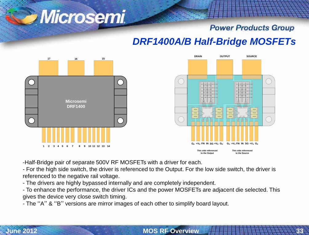
DRF1400A/B Half-Bridge MOSFETs
-Half-Bridge pair of separate 500V RF MOSFETs with a driver for each. - For the high side switch, the driver is referenced to the Output. For the low side switch, the driver is referenced to the negative rail voltage. - The drivers are highly bypassed internally and are completely independent. - To enhance the performance, the driver ICs and the power MOSFETs are adjacent die selected. This gives the device very close switch timing. - The “A” & “B” versions are mirror images of each other to simplify board layout.
MicrosemiDRF1400
1 2 3 4 5 6 7 8 9 10 11 12 13 14
151617
5600pF
5600pF
5600pF
5600pF
5600pF
5600pF
5600pF
5600pF
5600pF
5600pF
5600pF
5600pF
DRAIN SOURCEOUTPUT
GD +VD FN IN SG GD+VD GS +VS FN IN SG GS+VS
This side referenced to the Output
This side referenced to the Source

June 2012 MOS RF Overview 34
DRF Reference Designs
RF Output
Output Network
DRF1200
+300V DC Input+5 and +15 DC Input
13.56MHz Clock
RF Output
DRF1300
Output Network
+200 VDC Input
+5 and +15V VDC Input
13.56 MHz Clock
Push-Pull Transformer
-200V DC Input or Short
+200V DC Input or Short
24V DC InputOutput Network
RF Output
15V DC-DC Inverter 1 of 2
DRF1400 Reference Design Provides the end user with a learning tool and a development platform, allowing minimal time to market for new products. Note: All stated power levels are into a 50W Flat Load. Reference Designs come with a detailed application note, including circuit schematics, BOM, PCB Layout, theory of operation and test data.
DRF1200 Class-E DRF1300 Class-D
DRF1400 HB Class-D

June 2012 MOS RF Overview 35
DRF Design Guide
1uF1uF1uF
1uF1uF1uF
Transparent Case Outline, Fiberglass Renforced Ultem2300
Low Inductive Loop By-Pass Capacitors
Low Inductance Driver Output Loop
Solder Dam
DRAINSOURCEGND
SOURCEGND
+V +VccSGINDPSOURCEGND
SOURCEGND
BeO Substrate .040in. Thick Low Inductance Output Loop
Leads Not To Scale
1 2 3 4 5 6 7
8910
C2
C1
R1
R2
R3
R4
J2
GND
+VDS
+15V GND
X
X
X
X
XX
o oo
oo oJ1
C13
C12
R6200W
200W
C11
C10M
ICR
OSEM
ID
RF1200
BNC
X
X
X
X
Area for User Circuit Development
Full Ground Plane PCB
Cutout for Device Vdd By-Pass
Capacitors 2 Places
X
Control Signal input
NO CONTROL SIGNAL or LV POWER TRACE TO THE RIGHT OF THIS LINE
o = One Plated Through Hole X = 5 Plated Through Holes
o o
o o
Jumper Connecting By-Pass Capacitors to Ground, 2 Places
4 Traces for user Circuit Development
1
2
3
4
o o o o
o o o
The DRF Family of Devices are all based on a MOSFET Driver IC and a Power MOSFET. The Driver IC was developed here and is manufactured by Xfab in Germany the Power MOSFET is produced here in the Bend FAB. The DRF Devices are a complex RF Hybrid. However this Hybrid provides the Customer with Kilowatt Power Outputs controlled by Microprocessor level inputs. This is a Great Advantage to the Design Engineer and the Customer, in the case of the CC4017 for Huettinger this could represent an annual revenue of $30M. This all comes at a price and that is a lot of Customer Support and Training. The DRF Design Guide is a very lengthy “How To” Application Note, and will be the text we will use for future Training Sessions. This Publication and Training will help other companies become excited about the solutions these devices bring to their organization. In addition, the price tag also includes completely new and different Manufacturing Process, Device Test System, and Quality Assurance.
DRF1200
DRF1200 Evaluation Board

June 2012 MOS RF Overview 36