mos integrated circuit pd431000a · 2010-02-24 · 2 µpd431000a 32-pin plastic dip (600 mil)...
TRANSCRIPT
© 1990, 1993, 1995
DATA SHEET
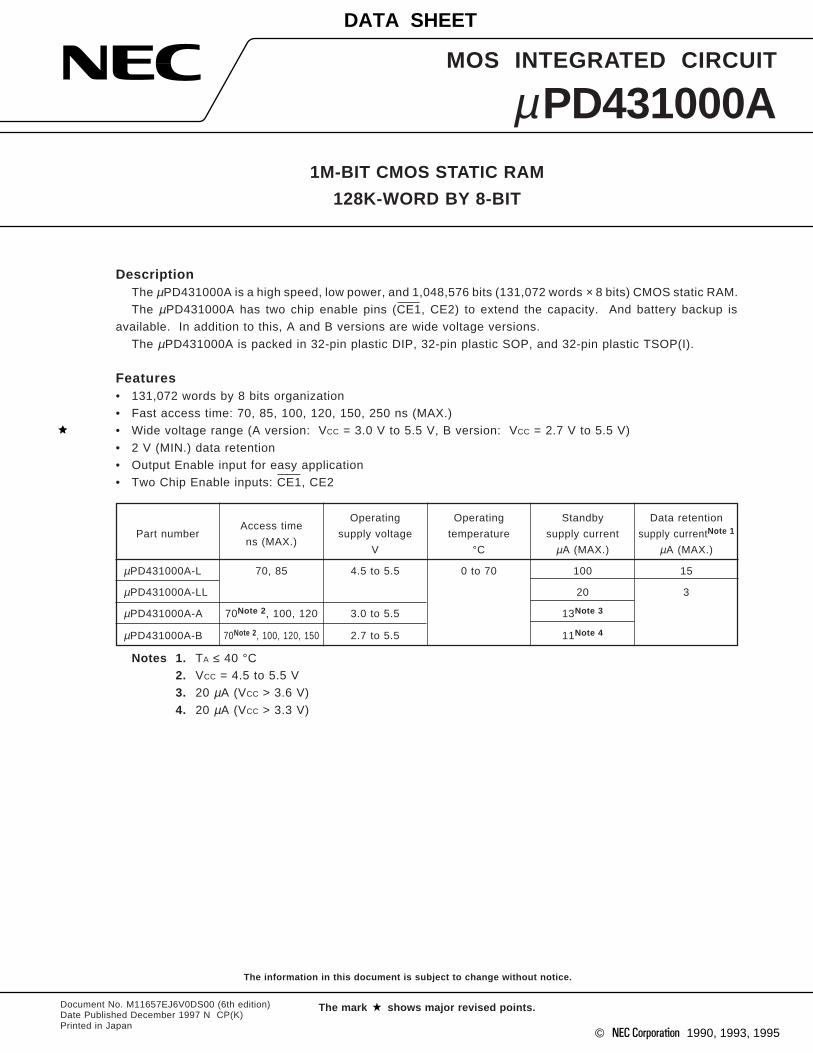
DescriptionThe µPD431000A is a high speed, low power, and 1,048,576 bits (131,072 words × 8 bits) CMOS static RAM.The µPD431000A has two chip enable pins (CE1, CE2) to extend the capacity. And battery backup is
available. In addition to this, A and B versions are wide voltage versions.
The µPD431000A is packed in 32-pin plastic DIP, 32-pin plastic SOP, and 32-pin plastic TSOP(I).
Features• 131,072 words by 8 bits organization• Fast access time: 70, 85, 100, 120, 150, 250 ns (MAX.)• Wide voltage range (A version: VCC = 3.0 V to 5.5 V, B version: VCC = 2.7 V to 5.5 V)
• 2 V (MIN.) data retention• Output Enable input for easy application• Two Chip Enable inputs: CE1, CE2
Access timeOperating Operating Standby Data retention
Part numberns (MAX.)
supply voltage temperature supply current supply currentNote 1
V °C µA (MAX.) µA (MAX.)
µPD431000A-L 70, 85 4.5 to 5.5 0 to 70 100 15
µPD431000A-LL 20 3
µPD431000A-A 70Note 2 , 100, 120 3.0 to 5.5 13Note 3
µPD431000A-B 70Note 2 , 100, 120, 150 2.7 to 5.5 11Note 4
Notes 1. TA ≤ 40 °C2. VCC = 4.5 to 5.5 V3. 20 µA (VCC > 3.6 V)
4. 20 µA (VCC > 3.3 V)
µ PD431000AMOS INTEGRATED CIRCUIT
The information in this document is subject to change without notice.
1M-BIT CMOS STATIC RAM
128K-WORD BY 8-BIT
The mark shows major revised points.Document No. M11657EJ6V0DS00 (6th edition)Date Published December 1997 N CP(K)Printed in Japan
2
µPD431000A
32-pin Plastic
DIP (600 mil)
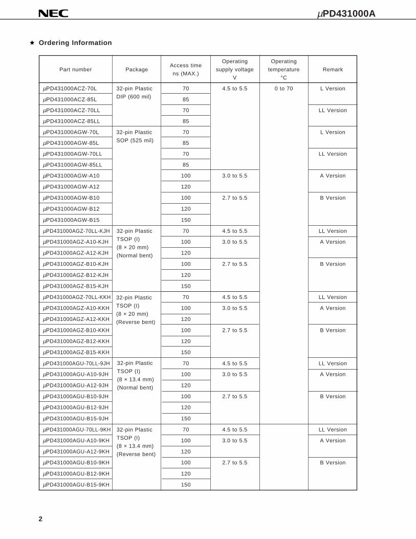
Ordering Information
Access timeOperating Operating
Part number Packagens (MAX.)
supply voltage temperature Remark
V °C
µPD431000ACZ-70L 70 4.5 to 5.5 0 to 70 L Version
µPD431000ACZ-85L 85
µPD431000ACZ-70LL 70 LL Version
µPD431000ACZ-85LL 85
µPD431000AGW-70L 70 L Version
µPD431000AGW-85L 85
µPD431000AGW-70LL 70 LL Version
µPD431000AGW-85LL 85
µPD431000AGW-A10 100 3.0 to 5.5 A Version
µPD431000AGW-A12 120
µPD431000AGW-B10 100 2.7 to 5.5 B Version
µPD431000AGW-B12 120
µPD431000AGW-B15 150
µPD431000AGZ-70LL-KJH 70 4.5 to 5.5 LL Version
µPD431000AGZ-A10-KJH 100 3.0 to 5.5 A Version
µPD431000AGZ-A12-KJH 120
µPD431000AGZ-B10-KJH 100 2.7 to 5.5 B Version
µPD431000AGZ-B12-KJH 120
µPD431000AGZ-B15-KJH 150
µPD431000AGZ-70LL-KKH 70 4.5 to 5.5 LL Version
µPD431000AGZ-A10-KKH 100 3.0 to 5.5 A Version
µPD431000AGZ-A12-KKH 120
µPD431000AGZ-B10-KKH 100 2.7 to 5.5 B Version
µPD431000AGZ-B12-KKH 120
µPD431000AGZ-B15-KKH 150
µPD431000AGU-70LL-9JH 70 4.5 to 5.5 LL Version
µPD431000AGU-A10-9JH 100 3.0 to 5.5 A Version
µPD431000AGU-A12-9JH 120
µPD431000AGU-B10-9JH 100 2.7 to 5.5 B Version
µPD431000AGU-B12-9JH 120
µPD431000AGU-B15-9JH 150
µPD431000AGU-70LL-9KH 70 4.5 to 5.5 LL Version
µPD431000AGU-A10-9KH 100 3.0 to 5.5 A Version
µPD431000AGU-A12-9KH 120
µPD431000AGU-B10-9KH 100 2.7 to 5.5 B Version
µPD431000AGU-B12-9KH 120
µPD431000AGU-B15-9KH 150
32-pin Plastic
SOP (525 mil)
32-pin Plastic
TSOP (I)
(8 × 20 mm)
(Normal bent)
32-pin Plastic
TSOP (I)
(8 × 20 mm)
(Reverse bent)
32-pin Plastic
TSOP (I)
(8 × 13.4 mm)
(Normal bent)
32-pin Plastic
TSOP (I)
(8 × 13.4 mm)
(Reverse bent)
3
µPD431000A
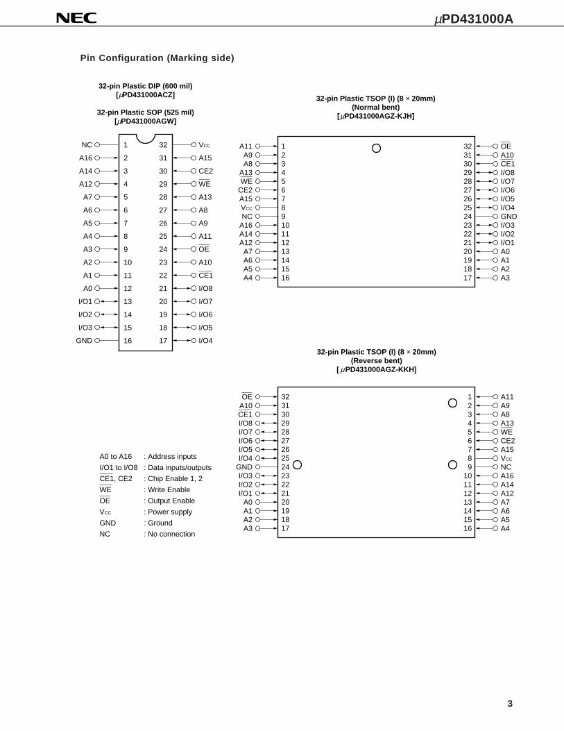
Pin Configuration (Marking side)
NC
A16
A14
A12
A7
A6
A5
A4
A3
A2
A1
A0
I/O1
I/O2
I/O3
GND
1
2
3
4
5
6
7
8
9
10
11
12
13
14
15
16
32
31
30
29
28
27
26
25
24
23
22
21
20
19
18
17
VCC
A15
CE2
WE
A13
A8
A9
A11
OE
A10
CE1
I/O8
I/O7
I/O6
I/O5
I/O4
µ
A11A9A8
A13WE
CE2A15VCC
NCA16A14A12
A7A6A5A4
12345678910111213141516
32313029282726252423222120191817
OEA10CE1I/O8I/O7I/O6I/O5I/O4GNDI/O3I/O2I/O1A0A1A2A3
µ
32-pin Plastic TSOP (I) (8 × 20mm)(Normal bent)
[ PD431000AGZ-KJH]
32-pin Plastic DIP (600 mil)[ PD431000ACZ]
32-pin Plastic SOP (525 mil)[ PD431000AGW]
OEA10CE1I/O8I/O7I/O6I/O5I/O4
GNDI/O3I/O2I/O1
A0A1A2A3
32313029282726252423222120191817
123456789
10111213141516
A11A9A8A13WECE2A15VCC
NCA16A14A12A7A6A5A4
32-pin Plastic TSOP (I) (8 × 20mm)(Reverse bent)
[ PD431000AGZ-KKH]
A0 to A16
I/O1 to I/O8
CE1, CE2
WE
OE
VCC
GND
NC
: Address inputs
: Data inputs/outputs
: Chip Enable 1, 2
: Write Enable
: Output Enable
: Power supply
: Ground
: No connection
µ
µ
4
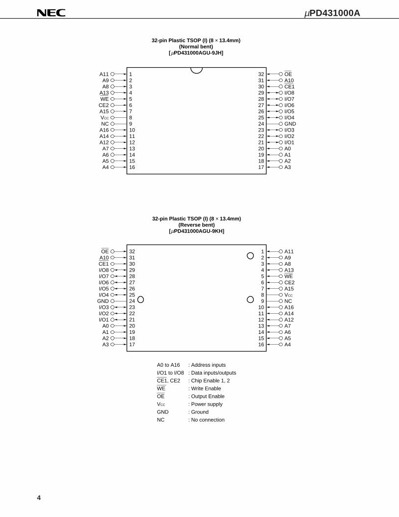
µPD431000A
A11A9A8
A13WE
CE2A15VCC
NCA16A14A12A7A6A5A4
12345678910111213141516
32313029282726252423222120191817
OEA10CE1I/O8I/O7I/O6I/O5I/O4GNDI/O3I/O2I/O1A0A1A2A3
µ
32-pin Plastic TSOP (I) (8 × 13.4mm)(Normal bent)
[ PD431000AGU-9JH]
OEA10CE1I/O8I/O7I/O6I/O5I/O4
GNDI/O3I/O2I/O1
A0A1A2A3
32313029282726252423222120191817
123456789
10111213141516
A11A9A8A13WECE2A15VCC
NCA16A14A12A7A6A5A4
32-pin Plastic TSOP (I) (8 × 13.4mm)(Reverse bent)
[ PD431000AGU-9KH]µ
A0 to A16
I/O1 to I/O8
CE1, CE2
WE
OE
VCC
GND
NC
: Address inputs
: Data inputs/outputs
: Chip Enable 1, 2
: Write Enable
: Output Enable
: Power supply
: Ground
: No connection

5
µPD431000A
Block Diagram
Truth Table
CE1 CE2 OE WE Mode I/O Supply current
H × × × ISB
× L × ×
L H H H Output disable
L H L H Read DOUT
L H × L Write DIN
Remark × : Don't care
Not selected High
impedance
Addressbuffer
Rowdecoder
Memory cell array1,048,576 bits
Input datacontroller
A0
A16
I/O1
I/O8
Sense/Switch
Column decoder
Output datacontroller
Address buffer
CE1
CE2
OE
WE
VCC
GND
ICCA
6
µPD431000A
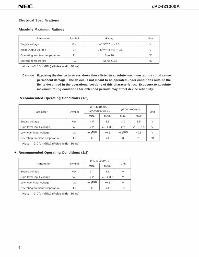
Electrical Specifications
Absolute Maximum Ratings
Supply voltage VCC –0.5Note to +7.0 V
Input/Output voltage VT –0.5Note to VCC + 0.5 V
Operating ambient temperature TA 0 to 70 °C
Storage temperature Tstg –55 to +125 °C
Note –3.0 V (MIN.) (Pulse width 30 ns)
Caution Exposing the device to stress above those listed in absolute maximum ratings could cause
permanent damage. The device is not meant to be operated under conditions outside the
limits described in the operational sections of this characteristics. Exposure to absolute
maximum rating conditions for extended periods may affect device reliability.
Recommended Operating Conditions (1/2)
µPD431000A-L
µPD431000A-LL
MIN. MAX. MIN. MAX
Supply voltage VCC 4.5 5.5 3.0 5.5 V
High level input voltage VIH 2.2 VCC + 0.5 2.2 VCC + 0.5 V
Low level input voltage VIL –0.3Note +0.8 –0.3Note +0.5 V
Operating ambient temperature TA 0 70 0 70 °C
Note –3.0 V (MIN.) (Pulse width 30 ns)
Recommended Operating Conditions (2/2)
µPD431000A-BParameter Symbol
MIN. MAX.Unit
Supply voltage VCC 2.7 5.5 V
High level input voltage VIH 2.2 VCC + 0.5 V
Low level input voltage VIL –0.3Note +0.5 V
Operating ambient temperature TA 0 70 °C
Note –3.0 V (MIN.) (Pulse width 30 ns)
Parameter Symbol Rating Unit
µPD431000A-AParameter Symbol Unit
7
µPD431000A
Standby supplycurrent
High leveloutput voltage
Low leveloutput voltage
MIN. TYP. MAX. MIN. TYP. MAX. MIN. TYP. MAX.
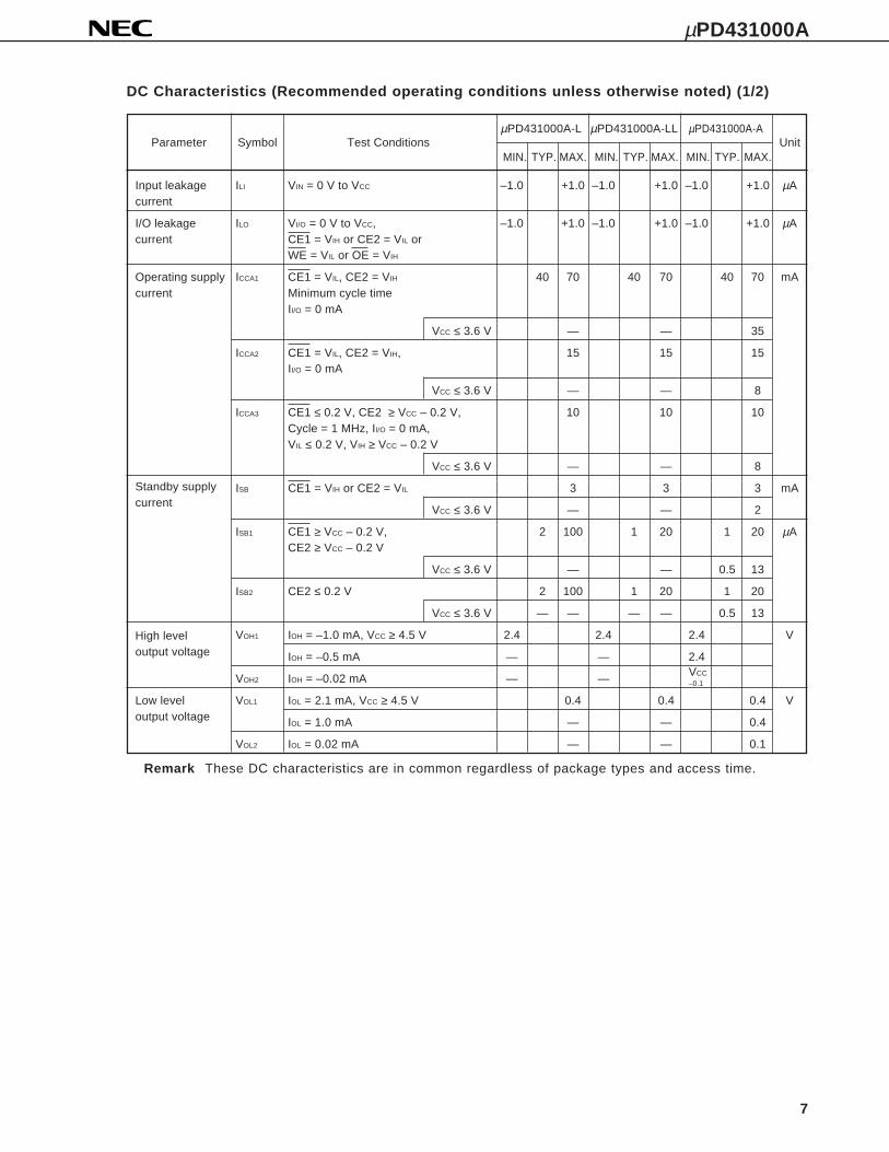
DC Characteristics (Recommended operating conditions unless otherwise noted) (1/2)
µPD431000A-L µPD431000A-LL µPD431000A-AParameter Symbol Test Conditions Unit
Input leakage ILI VIN = 0 V to VCC –1.0 +1.0 –1.0 +1.0 –1.0 +1.0 µAcurrent
I/O leakage ILO VI/O = 0 V to VCC, –1.0 +1.0 –1.0 +1.0 –1.0 +1.0 µAcurrent CE1 = VIH or CE2 = VIL or
WE = VIL or OE = VIH
Operating supply ICCA1 CE1 = VIL, CE2 = VIH 40 70 40 70 40 70 mAcurrent Minimum cycle time
II/O = 0 mA
VCC ≤ 3.6 V — — 35
ICCA2 CE1 = VIL, CE2 = VIH, 15 15 15II/O = 0 mA
VCC ≤ 3.6 V — — 8
ICCA3 CE1 ≤ 0.2 V, CE2 ≥ VCC – 0.2 V, 10 10 10Cycle = 1 MHz, II/O = 0 mA,VIL ≤ 0.2 V, VIH ≥ VCC – 0.2 V
VCC ≤ 3.6 V — — 8
ISB CE1 = VIH or CE2 = VIL 3 3 3 mA
VCC ≤ 3.6 V — — 2
ISB1 CE1 ≥ VCC – 0.2 V, 2 100 1 20 1 20 µACE2 ≥ VCC – 0.2 V
VCC ≤ 3.6 V — — 0.5 13
ISB2 CE2 ≤ 0.2 V 2 100 1 20 1 20
VCC ≤ 3.6 V — — — — 0.5 13
VOH1 IOH = –1.0 mA, VCC ≥ 4.5 V 2.4 2.4 2.4 V
IOH = –0.5 mA — — 2.4
VOH2 IOH = –0.02 mA — —
VOL1 IOL = 2.1 mA, VCC ≥ 4.5 V 0.4 0.4 0.4 V
IOL = 1.0 mA — — 0.4
VOL2 IOL = 0.02 mA — — 0.1
Remark These DC characteristics are in common regardless of package types and access time.
VCC–0.1

8
µPD431000A
DC Characteristics (Recommended operating conditions unless otherwise noted) (2/2)
µPD431000A-BParameter Symbol Test Conditions Unit
Input leakage ILI VIN = 0 V to VCC –1.0 +1.0 µAcurrent
I/O leakage ILO VI/O = 0 V to VCC, –1.0 +1.0 µAcurrent CE1 = VIH or CE2 = VIL or
WE = VIL or OE = VIH
Operating supply ICCA1 CE1 = VIL, CE2 = VIH 40 70 mAcurrent Minimum cycle time
II/O = 0 mAVCC ≤ 3.3 V — 30
ICCA2 CE1 = VIL, CE2 = VIH, 15II/O = 0 mA
VCC ≤ 3.3 V 7
ICCA3 CE1 ≤ 0.2 V, CE2 ≥ VCC – 0.2 V, 10Cycle = 1 MHz, II/O = 0 mA,VIL ≤ 0.2 V, VIH ≥ VCC – 0.2 V
VCC ≤ 3.3 V 7
ISB CE1 = VIH or CE2 = VIL 3 mA
VCC ≤ 3.3 V 2
ISB1 CE1 ≥ VCC – 0.2 V, 1 20 µACE2 ≥ VCC – 0.2 V
VCC ≤ 3.3 V 0.5 11
ISB2 CE2 ≤ 0.2 V 1 20
VCC ≤ 3.3 V 0.5 11
VOH1 IOH = –1.0 mA, VCC ≥ 4.5 V 2.4 V
IOH = –0.5 mA 2.4
VOH2 IOH = –0.02 mA VCC – 0.1
VOL1 IOL = 2.1 mA, VCC ≥ 4.5 V 0.4 V
IOL = 1.0 mA 0.4
VOL2 IOL = 0.02 mA 0.1
Remark These DC characteristics are in common regardless of package types and access time.
Capacitance (T A = 25 °C, f = 1 MHz)
Parameter Symbol Test conditions MIN. TYP. MAX. Unit
Input capacitance CIN VIN = 0 V 6 pF
Input/Output capacitance CI/O VI/O = 0 V 10 pF
Remarks 1. VIN: Input voltage
2. These parameters are periodically sampled and not 100 % tested.
Low leveloutput voltage
High leveloutput voltage
Standby supplycurrent
MIN. TYP. MAX.

9
µPD431000A
AC Characteristics (Recommended operating conditions unless otherwise noted)
AC Test Conditions
Input waveform (Rise/fall time ≤ 5 ns)
Input pulse levels
0.8 V to 2.2 V : µPD431000A-L, 431000A-LL
0.5 V to 2.2 V : µPD431000A-A, 431000A-B
Output waveform
Output load
AC characteristics should be measured with the following output load conditions.
Part numberOutput load conditions
tAA, tCO1, tCO2, tOE, tOH tLZ1, tLZ2, tOLZ, tHZ1, tHZ2, tOHZ, tWHZ, tOW
µPD431000A-A10, 431000A-A12 1TTL + 50 pF 1TTL + 5 pF
µPD431000A-B10, 431000A-B12
µPD431000A-B15 1TTL + 100 pF 1TTL + 5 pF
µPD431000A-L, 431000A-LL See Figure 1 See Figure 2
Figure 1 Figure 2
Remark CL includes capacitances of the probe and jig, and stray capacitances.
1.5 V 1.5 VTest points
1.5 V 1.5 VTest points
+5 V
I/O (Output)
1.8 kΩ
100 pFCL
990 Ω
+5 V
I/O (Output)
1.8 kΩ
5 pFCL
990 Ω
10
µPD431000A
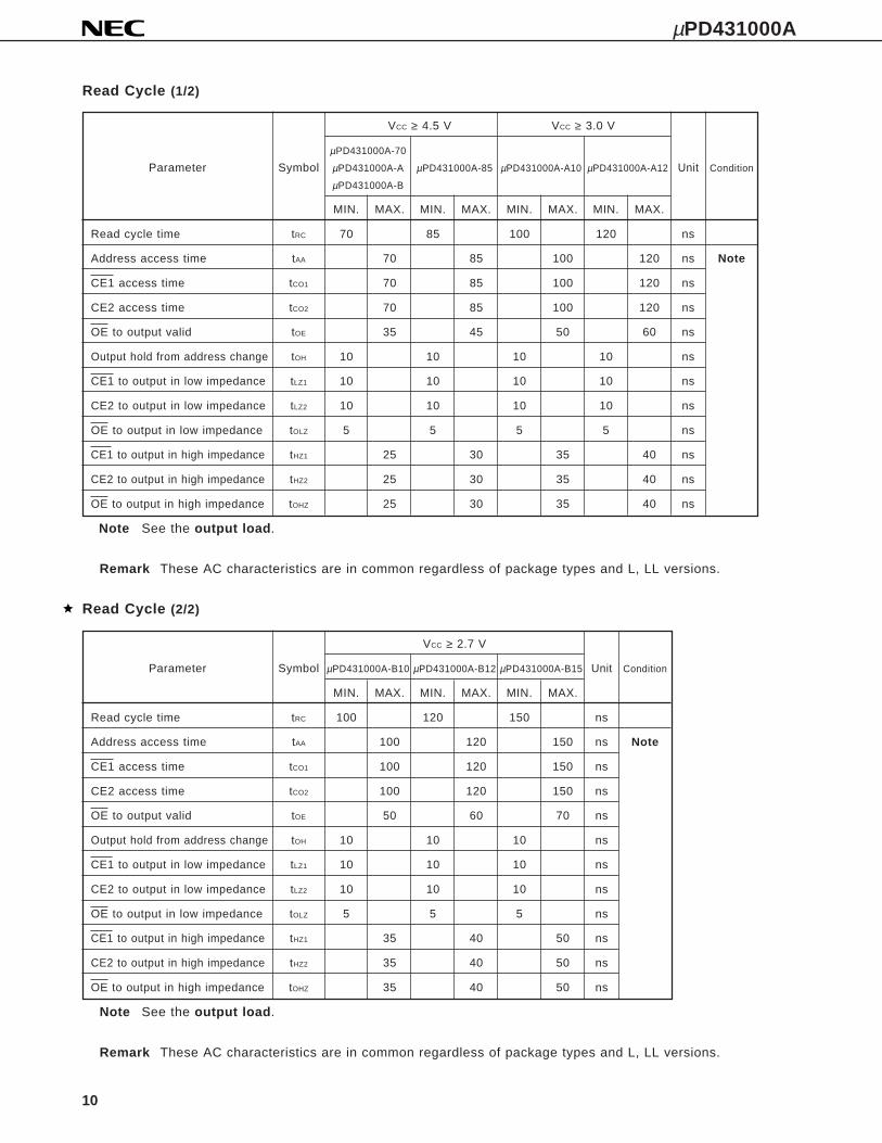
Read Cycle (1/2)
VCC ≥ 4.5 V VCC ≥ 3.0 V
µPD431000A-70
Parameter Symbol µPD431000A-A µPD431000A-85 µPD431000A-A10 µPD431000A-A12 Unit Condition
µPD431000A-B
MIN. MAX. MIN. MAX. MIN. MAX. MIN. MAX.
Read cycle time tRC 70 85 100 120 ns
Address access time tAA 70 85 100 120 ns Note
CE1 access time tCO1 70 85 100 120 ns
CE2 access time tCO2 70 85 100 120 ns
OE to output valid tOE 35 45 50 60 ns
Output hold from address change tOH 10 10 10 10 ns
CE1 to output in low impedance tLZ1 10 10 10 10 ns
CE2 to output in low impedance tLZ2 10 10 10 10 ns
OE to output in low impedance tOLZ 5 5 5 5 ns
CE1 to output in high impedance tHZ1 25 30 35 40 ns
CE2 to output in high impedance tHZ2 25 30 35 40 ns
OE to output in high impedance tOHZ 25 30 35 40 ns
Note See the output load .
Remark These AC characteristics are in common regardless of package types and L, LL versions.
Read Cycle (2/2)
VCC ≥ 2.7 V
Parameter Symbol µPD431000A-B10 µPD431000A-B12 µPD431000A-B15 Unit Condition
MIN. MAX. MIN. MAX. MIN. MAX.
Read cycle time tRC 100 120 150 ns
Address access time tAA 100 120 150 ns Note
CE1 access time tCO1 100 120 150 ns
CE2 access time tCO2 100 120 150 ns
OE to output valid tOE 50 60 70 ns
Output hold from address change tOH 10 10 10 ns
CE1 to output in low impedance tLZ1 10 10 10 ns
CE2 to output in low impedance tLZ2 10 10 10 ns
OE to output in low impedance tOLZ 5 5 5 ns
CE1 to output in high impedance tHZ1 35 40 50 ns
CE2 to output in high impedance tHZ2 35 40 50 ns
OE to output in high impedance tOHZ 35 40 50 ns
Note See the output load .
Remark These AC characteristics are in common regardless of package types and L, LL versions.
11
µPD431000A
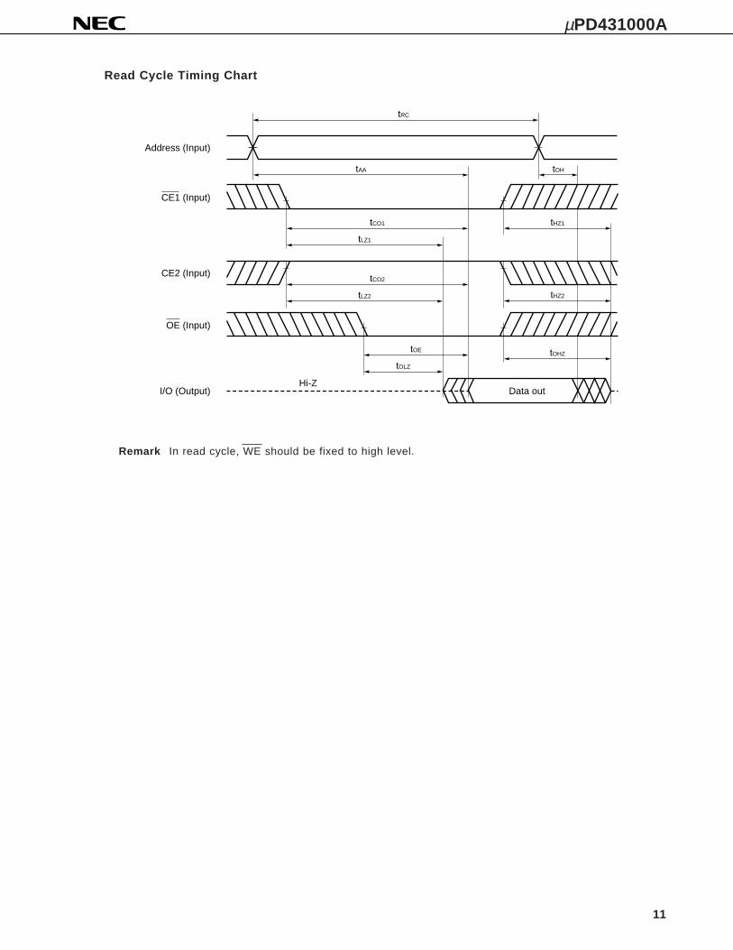
Read Cycle Timing Chart
Remark In read cycle, WE should be fixed to high level.
tHZ2
tRC
tOH
tHZ1
tOLZ
tOE
tLZ2
tCO2
tLZ1
tCO1
tOHZ
tAA
Hi-ZData out
OE (Input)
CE2 (Input)
CE1 (Input)
Address (Input)
I/O (Output)
12
µPD431000A
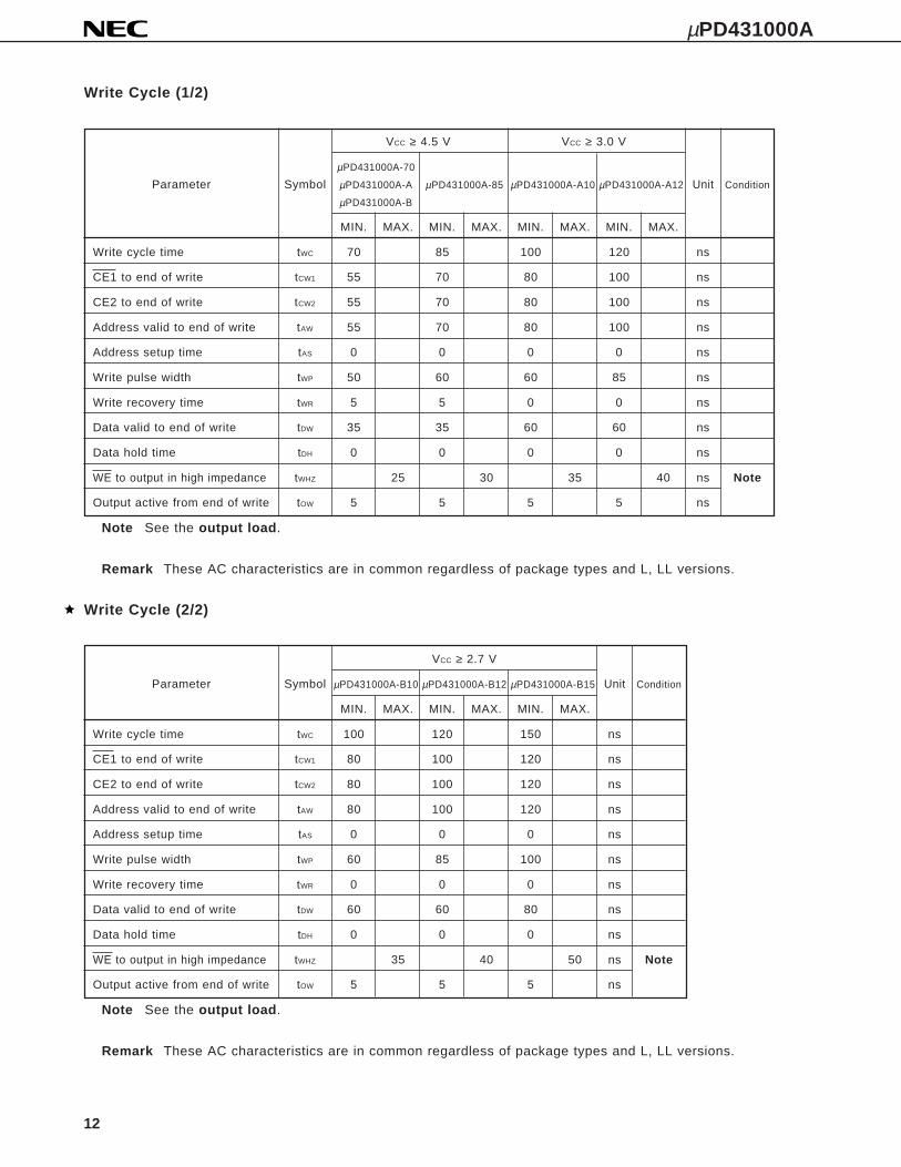
Write Cycle (1/2)
VCC ≥ 4.5 V VCC ≥ 3.0 V
µPD431000A-70
Parameter Symbol µPD431000A-A µPD431000A-85 µPD431000A-A10 µPD431000A-A12 Unit Condition
µPD431000A-B
MIN. MAX. MIN. MAX. MIN. MAX. MIN. MAX.
Write cycle time tWC 70 85 100 120 ns
CE1 to end of write tCW1 55 70 80 100 ns
CE2 to end of write tCW2 55 70 80 100 ns
Address valid to end of write tAW 55 70 80 100 ns
Address setup time tAS 0 0 0 0 ns
Write pulse width tWP 50 60 60 85 ns
Write recovery time tWR 5 5 0 0 ns
Data valid to end of write tDW 35 35 60 60 ns
Data hold time tDH 0 0 0 0 ns
WE to output in high impedance tWHZ 25 30 35 40 ns Note
Output active from end of write tOW 5 5 5 5 ns
Note See the output load .
Remark These AC characteristics are in common regardless of package types and L, LL versions.
Write Cycle (2/2)
VCC ≥ 2.7 V
Parameter Symbol µPD431000A-B10 µPD431000A-B12 µPD431000A-B15 Unit Condition
MIN. MAX. MIN. MAX. MIN. MAX.
Write cycle time tWC 100 120 150 ns
CE1 to end of write tCW1 80 100 120 ns
CE2 to end of write tCW2 80 100 120 ns
Address valid to end of write tAW 80 100 120 ns
Address setup time tAS 0 0 0 ns
Write pulse width tWP 60 85 100 ns
Write recovery time tWR 0 0 0 ns
Data valid to end of write tDW 60 60 80 ns
Data hold time tDH 0 0 0 ns
WE to output in high impedance tWHZ 35 40 50 ns Note
Output active from end of write tOW 5 5 5 ns
Note See the output load .
Remark These AC characteristics are in common regardless of package types and L, LL versions.
13
µPD431000A
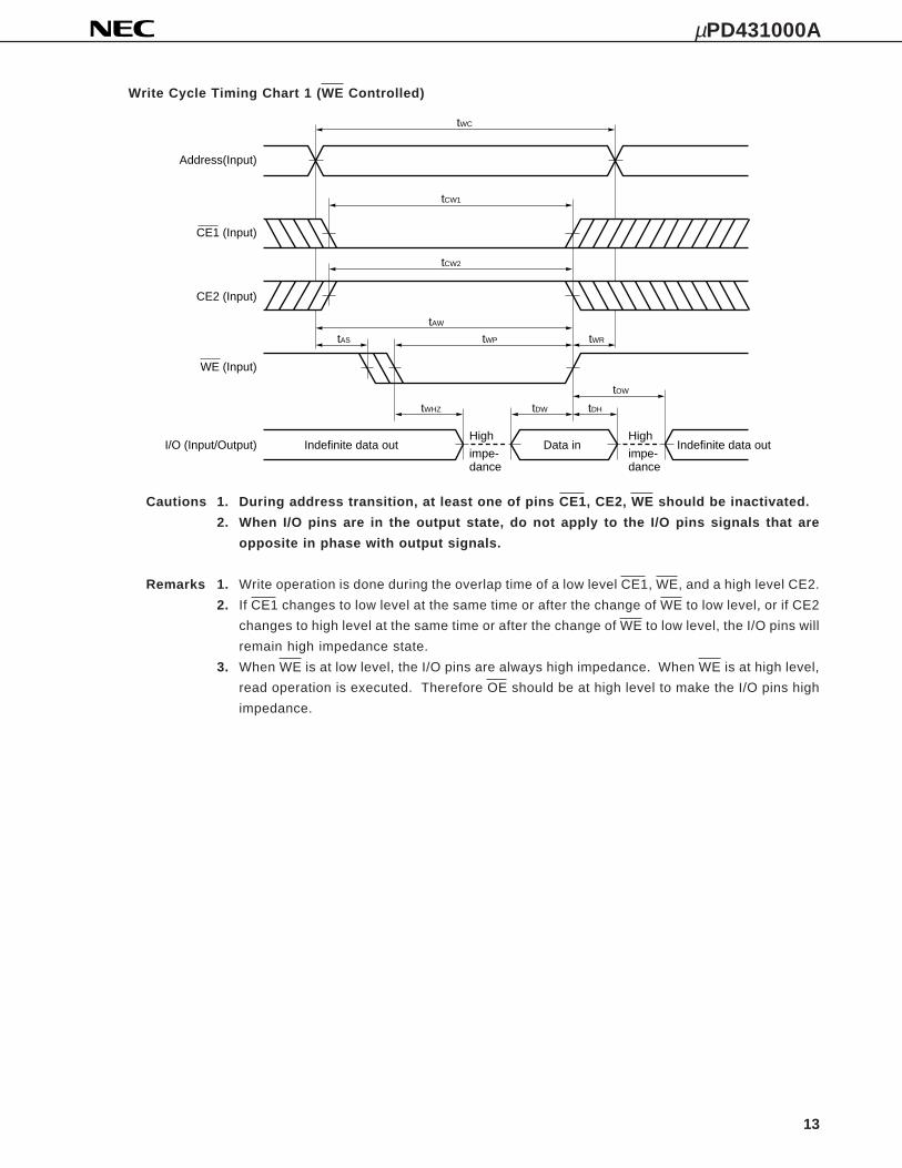
Write Cycle Timing Chart 1 (WE Controlled)
Cautions 1. During address transition, at least one of pins CE1, CE2, WE should be inactivated.
2. When I/O pins are in the output state, do not apply to the I/O pins signals that are
opposite in phase with output signals.
Remarks 1. Write operation is done during the overlap time of a low level CE1, WE, and a high level CE2.
2. If CE1 changes to low level at the same time or after the change of WE to low level, or if CE2
changes to high level at the same time or after the change of WE to low level, the I/O pins will
remain high impedance state.
3. When WE is at low level, the I/O pins are always high impedance. When WE is at high level,
read operation is executed. Therefore OE should be at high level to make the I/O pins high
impedance.
tWC
tCW1
tAW
tWPtAS tWR
tWHZ tDW tDH
tOW
Indefinite data outHigh
impe-dance
High
impe-dance
Data in Indefinite data out
Address(Input)
CE1 (Input)
WE (Input)
I/O (Input/Output)
CE2 (Input)
tCW2
14
µPD431000A
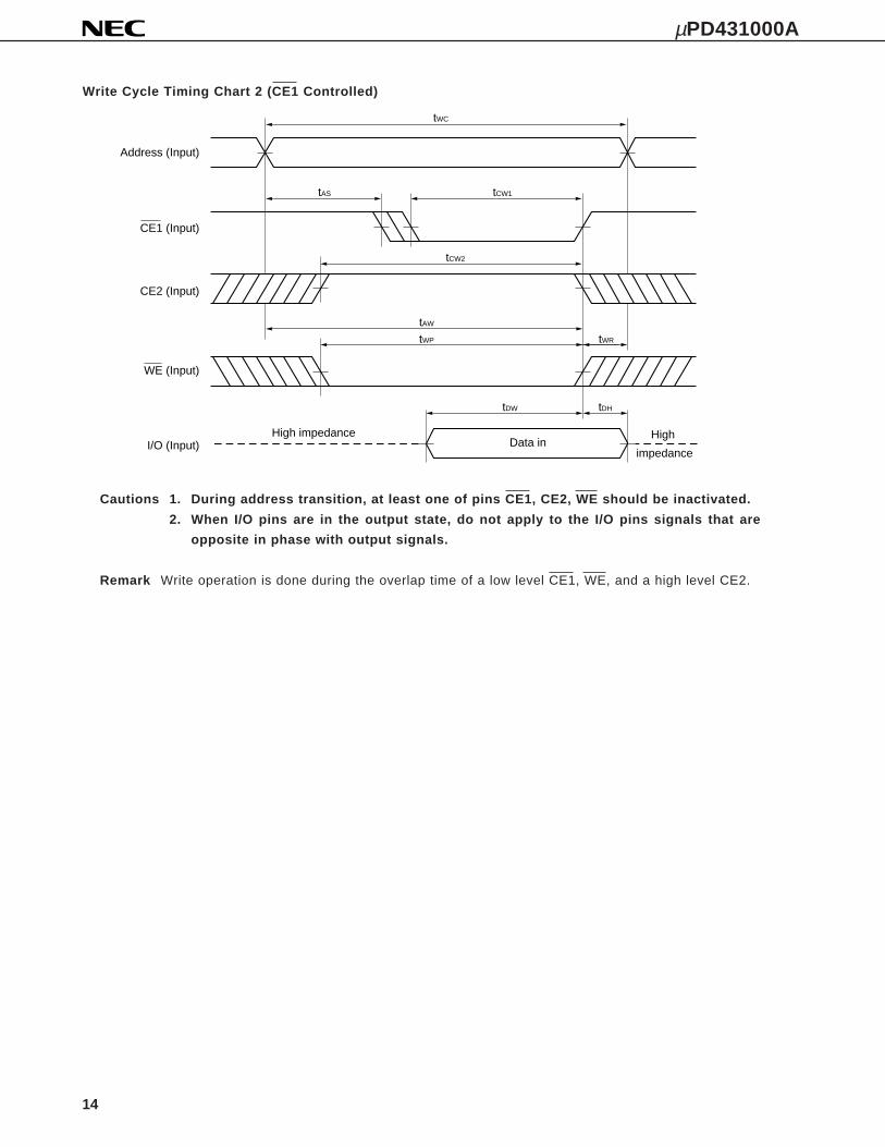
Cautions 1. During address transition, at least one of pins CE1, CE2, WE should be inactivated.
2. When I/O pins are in the output state, do not apply to the I/O pins signals that are
opposite in phase with output signals.
Remark Write operation is done during the overlap time of a low level CE1, WE, and a high level CE2.
Write Cycle Timing Chart 2 (CE1 Controlled)
tWC
tAS tCW1
tAW
tWP tWR
tDW tDH
Data inHigh impedance
Address (Input)
CE1 (Input)
WE (Input)
I/O (Input)High
impedance
CE2 (Input)
tCW2
15
µPD431000A
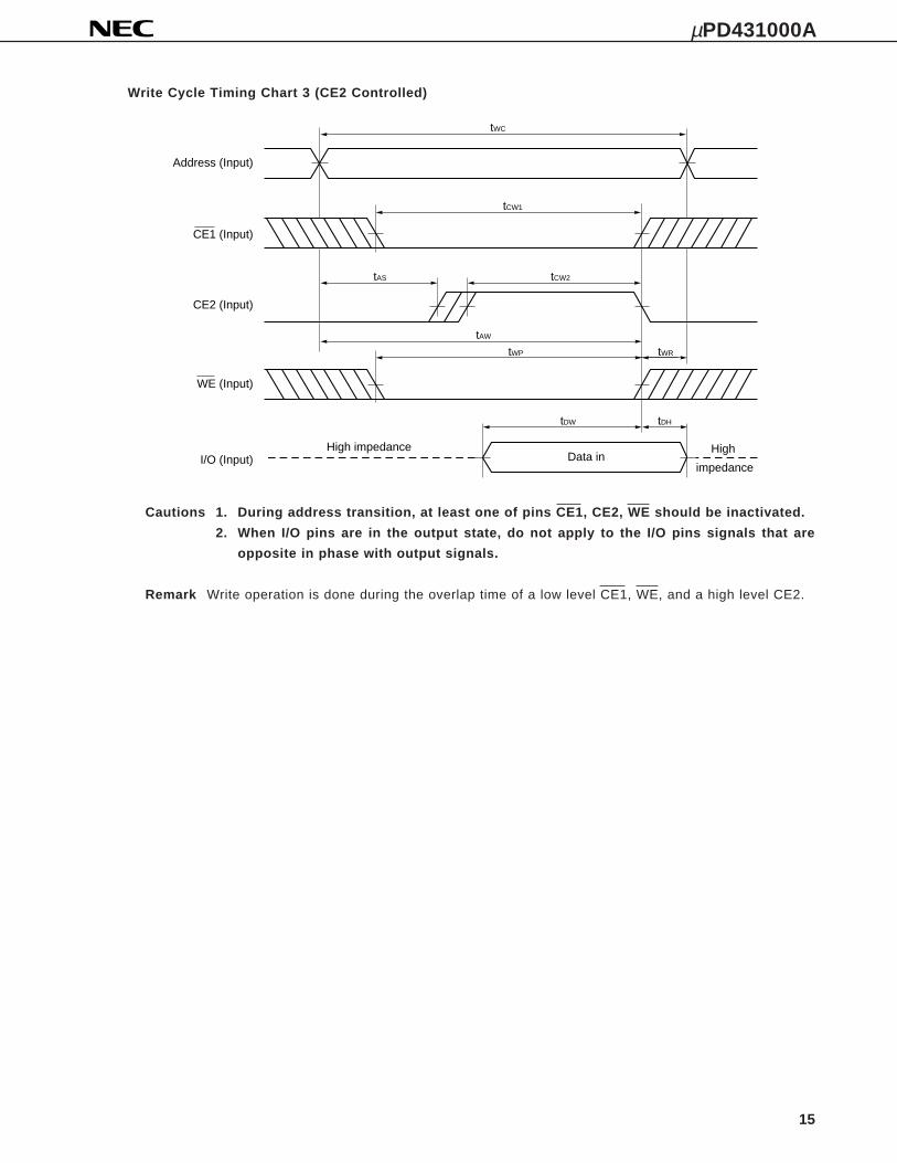
Write Cycle Timing Chart 3 (CE2 Controlled)
tWC
tAS tCW2
tAW
tWP tWR
tDW tDH
Data inHigh impedance
Address (Input)
CE2 (Input)
WE (Input)
I/O (Input)High
impedance
CE1 (Input)
tCW1
Cautions 1. During address transition, at least one of pins CE1, CE2, WE should be inactivated.
2. When I/O pins are in the output state, do not apply to the I/O pins signals that are
opposite in phase with output signals.
Remark Write operation is done during the overlap time of a low level CE1, WE, and a high level CE2.

16
µPD431000A
Low V CC Data Retention Characteristics
L Version ( µPD431000A-L: T A = 0 to 70 °C)
Parameter Symbol Test conditions MIN. TYP. MAX. Unit
Data retention supply voltage VCCDR1 CE1 ≥ VCC – 0.2 V, CE2 ≥ VCC – 0.2 V 2.0 5.5 V
VCCDR2 CE2 ≤ 0.2 V 2.0 5.5
Data retention supply current ICCDR1 VCC = 3.0 V, CE1 ≥ VCC – 0.2 V, 1 50Note µA
CE2 ≥ VCC – 0.2 V or CE2 ≤ 0.2 V
ICCDR2 VCC = 3.0 V, CE2 ≤ 0.2 V 1 50Note
Chip deselection to data tCDR 0 ns
retention mode
Operation recovery time tR 5 ms
Note 15 µA (TA ≤ 40 °C)
LL Version, A Version, and B Version ( µPD431000A-LL, 431000A-A, 431000A-B: T A = 0 to 70 °C)
Parameter Symbol Test conditions MIN. TYP. MAX. Unit
Data retention supply voltage VCCDR1 CE1 ≥ VCC – 0.2 V, CE2 ≥ VCC – 0.2 V 2.0 5.5 V
VCCDR2 CE2 ≤ 0.2 V 2.0 5.5
Data retention supply current ICCDR1 VCC = 3.0 V, CE1 ≥ VCC – 0.2 V, 0.5 10Note µA
CE2 ≥ VCC – 0.2 V or CE2 ≤ 0.2 V
ICCDR2 VCC = 3.0 V, CE2 ≤ 0.2 V 0.5 10Note
Chip deselection to data tCDR 0 ns
retention mode
Operation recovery time tR 5 ms
Note 3 µA (TA ≤ 40 °C)
17
µPD431000A
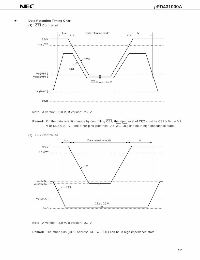
Data Retention Timing Chart
(1) CE1 Controlled
Note A version: 3.0 V, B version: 2.7 V
Remark On the data retention mode by controlling CE1, the input level of CE2 must be CE2 ≥ VCC – 0.2
V or CE2 ≤ 0.2 V. The other pins (Address, I/O, WE, OE) can be in high impedance state.
(2) CE2 Controlled
Note A version: 3.0 V, B version: 2.7 V
Remark The other pins (CE1, Address, I/O, WE, OE) can be in high impedance state.
tCDR Data retention mode
5.0 V
VIH (MIN. )VCCDR (MIN. )
VIL (MAX. )
tR
VCC
CE1
CE1 ≥ VCC – 0.2 V
GND
4.5 VNote
tCDR Data retention mode
5.0 V
VIH (MIN. )VCCDR (MIN. )
VIL (MAX. )
tR
VCC
CE2
CE2 ≤ 0.2 V
GND
4.5 VNote
18
µPD431000A
Package Drawings
32PIN PLASTIC DIP (600 mil)
NOTES
1) Each lead centerline is located within 0.25 mm (0.01 inch) of its true position (T.P.) at maximum material condition.
ITEM MILLIMETERS INCHES
A 40.64 MAX. 1.600 MAX.
B 1.27 MAX. 0.050 MAX.
C 2.54 (T.P.) 0.100 (T.P.)
D 0.50±0.10 0.020+0.004–0.005
F 1.1 MIN. 0.043 MIN.
G 3.2±0.3 0.126±0.012
J 5.08 MAX. 0.200 MAX.
K 15.24 (T.P.) 0.600 (T.P.)
M 0.25 0.010+0.004–0.003
N 0.25 0.01
H 0.51 MIN. 0.020 MIN.
I 4.31 MAX. 0.170 MAX.
L 13.2 0.520
+0.10–0.05
2) Item "K" to center of leads when formed parallel.
P32C-100-600A-1
R 0~15° 0~15°P 0.9 MIN. 0.035 MIN.
32 17
1 16
N
B
I
M RM
C
D
F
H
G
A
J
K
LP

19
µPD431000A
32 PIN PLASTIC SOP (525 mil)
A
32 17
detail of lead end
1 16 3°+
7° –3°
P32GW-50-525A
ITEM MILLIMETERS INCHES
A
B
C
D
E
F
G
H
I
J
K
20.61 MAX.
1.27 (T.P.)
2.95 MAX.
2.7
14.1±0.3
0.78 MAX.
0.812 MAX.
0.006
0.117 MAX.
0.555±0.012
0.445
0.031 MAX.
NOTE
L
M 0.12
0.8±0.2
1.4±0.2
11.3
0.005
0.031+0.009–0.008
Each lead centerline is located within 0.12mm (0.005 inch) of its true position (T.P.) atmaximum material condition.
0.055±0.008
0.106
0.050 (T.P.)
0.20 0.008
N 0.10 0.004
0.0160.40
0.15±0.05
+0.004–0.002
+0.10–0.05
+0.004–0.003
+0.10–0.05
F
D M
C
M
BN
GE
H
K
L
JI
20
µPD431000A
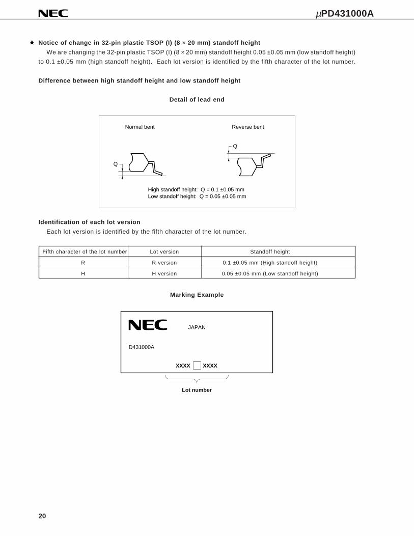
Notice of change in 32-pin plastic TSOP (I) (8 × 20 mm) standoff height
We are changing the 32-pin plastic TSOP (I) (8 × 20 mm) standoff height 0.05 ±0.05 mm (low standoff height)
to 0.1 ±0.05 mm (high standoff height). Each lot version is identified by the fifth character of the lot number.
Difference between high standoff height and low standoff height
Detail of lead end
Normal bent Reverse bent
Q
High standoff height: Q = 0.1 ±0.05 mmLow standoff height: Q = 0.05 ±0.05 mm
Q
Identification of each lot version
Each lot version is identified by the fifth character of the lot number.
Fifth character of the lot number Lot version Standoff height
R R version 0.1 ±0.05 mm (High standoff height)
H H version 0.05 ±0.05 mm (Low standoff height)
Marking Example
JAPAN
Lot number
D431000A
XXXX XXXX
21
µPD431000A
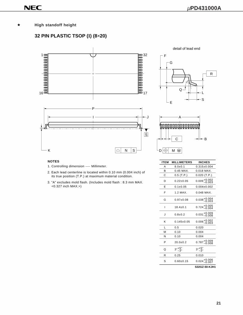
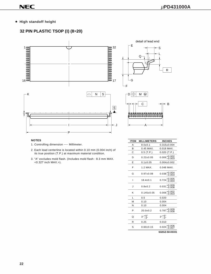
High standoff height
NOTES
32 PIN PLASTIC TSOP (I) (8×20)
ITEM MILLIMETERS INCHES
A
B
C
E
I
8.0±0.1
0.5 (T.P.)
0.1±0.05
0.45 MAX.
K
1.2 MAX.
18.4±0.1
0.145±0.05
F
0.10M
0.315±0.004
0.018 MAX.
0.004±0.002
0.724
0.006
0.048 MAX.
0.004
0.020 (T.P.)
D 0.22±0.05 0.009
2. Each lead centerline is located within 0.10 mm (0.004 inch) of its true position (T.P.) at maximum material condition.
3. "A" excludes mold flash. (Includes mold flash : 8.3 mm MAX. <0.327 inch MAX.>)
C
R
D MM
L
+0.002–0.003
0.97±0.08G 0.038+0.004–0.003
+0.005–0.004
L 0.5 0.020
0.10N 0.004
P 20.0±0.2 0.787+0.009–0.008
Q 3° 3°+5°–3°
+5°–3°
0.25R 0.010
S32GZ-50-KJH1
S 0.60±0.15 0.024+0.006–0.007
+0.002–0.003
J 0.8±0.2 0.031+0.009–0.008
1
16
32
17
S
P
G
F
ES
Q
NK
I
B
detail of lead end
J A
S
1. Controlling dimension Millimeter.
22
µPD431000A
High standoff height
NOTES
32 PIN PLASTIC TSOP (I) (8×20)
ITEM MILLIMETERS INCHES
A
B
C
E
I
8.0±0.1
0.5 (T.P.)
0.1±0.05
0.45 MAX.
K
1.2 MAX.
18.4±0.1
0.145±0.05
F
0.10M
0.315±0.004
0.018 MAX.
0.004±0.002
0.724
0.006
0.048 MAX.
0.004
0.020 (T.P.)
D 0.22±0.05 0.009
2. Each lead centerline is located within 0.10 mm (0.004 inch) of its true position (T.P.) at maximum material condition.
3. "A" excludes mold flash. (Includes mold flash : 8.3 mm MAX. <0.327 inch MAX.>).
C
R
D MM
G
+0.002–0.003
0.97±0.08G 0.038+0.004–0.003
+0.005–0.004
L 0.5 0.020
0.10N 0.004
P 20.0±0.2 0.787+0.009–0.008
Q 3° 3°+5°–3°
+5°–3°
0.25R 0.010
S32GZ-50-KKH1
S 0.60±0.15 0.024+0.006–0.007
+0.002–0.003
J 0.8±0.2 0.031+0.009–0.008
1
16
32
17
SN
B
A
F
E
Q
S
L
K
I
P
J
detail of lead end
S
1. Controlling dimension Millimeter.
23
µPD431000A
32 PIN PLASTIC TSOP (I) (8×20)
S32GZ-50-KJH-3
ITEM MILLIMETERS INCHESNOTES
(1) Each lead centerline is located within 0.08 mm (0.003 inch) of its true position (T.P.) at maximum material condition.
DN
I 18.4±0.2 0.724+0.009–0.008
K 0.125 0.005
L 0.5±0.1 0.020 +0.004–0.005
detail of lead end
R
C B
B
C 0.5 (T.P.)
0.45 MAX. 0.018 MAX.
0.020 (T.P.)
D
G 1.02 MAX.
0.20±0.10 0.008±0.004
0.041 MAX.
J 0.8±0.2 0.031+0.009–0.008
Q 0.05±0.05 0.002±0.002
R
S 1.1 MAX.
5°±5° 5°±5°0.044 MAX.
+0.10–0.05
+0.004–0.002
(2) "A" excIudes mold flash. (Includes mold flash : 8.3 mm MAX. < 0.327 inch MAX.>)
MM
Q
G
L
K
1
16
32
17
S
P
I J
H
A
A 8.0±0.1 0.315±0.004
H 19.0±0.2 0.748±0.008
M
N 0.10
0.08 0.003
0.004
P 20.0±0.2 0.787 +0.009–0.008
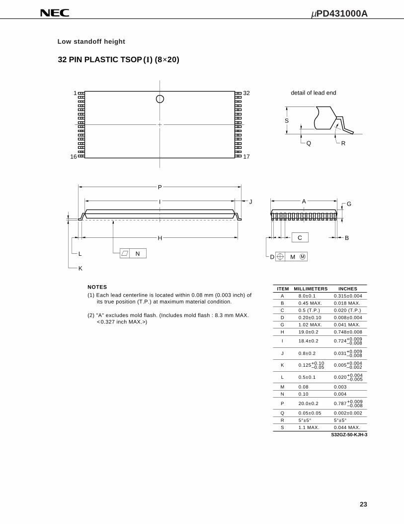
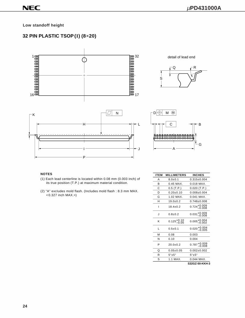
Low standoff height
24
µPD431000A
32 PIN PLASTIC TSOP (I) (8×20)
S32GZ-50-KKH-3
ITEM MILLIMETERS INCHESNOTES
(1) Each lead centerline is located within 0.08 mm (0.003 inch) of its true position (T.P.) at maximum material condition.
DN
I 18.4±0.2 0.724+0.009–0.008
K 0.125 0.005
L 0.5±0.1 0.020 +0.004–0.005
detail of lead end
R
C B
B
C 0.5 (T.P.)
0.45 MAX. 0.018 MAX.
0.020 (T.P.)
D
G 1.02 MAX.
0.20±0.10 0.008±0.004
0.041 MAX.
J 0.8±0.2 0.031+0.009–0.008
Q 0.05±0.05 0.002±0.002
R
S 1.1 MAX.
5°±5° 5°±5°0.044 MAX.
+0.10–0.05
+0.004–0.002
(2) "A" excIudes mold flash. (Includes mold flash : 8.3 mm MAX. < 0.327 inch MAX.>)
MM
Q
G
L
K
J
A 8.0±0.1 0.315±0.004
H 19.0±0.2 0.748±0.008
M
N 0.10
0.08 0.003
0.004
P 20.0±0.2 0.787 +0.009–0.008
1
16
32
17
S
P
I
H
A
Low standoff height
25
µPD431000A
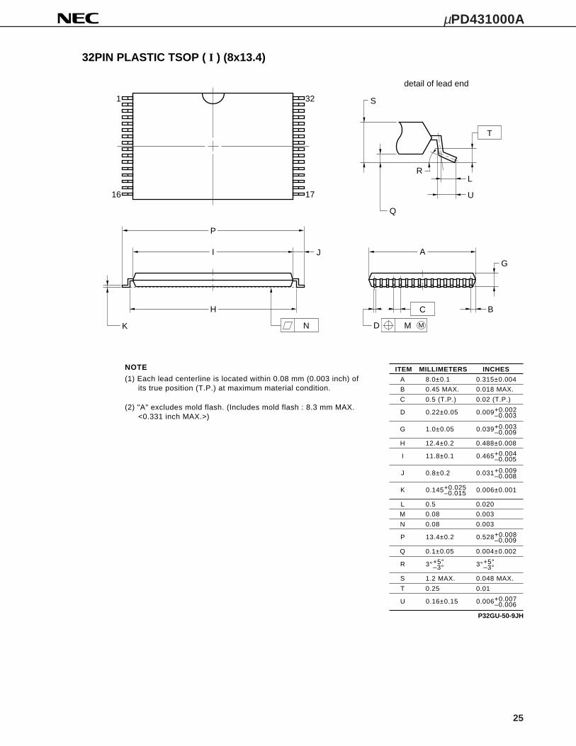
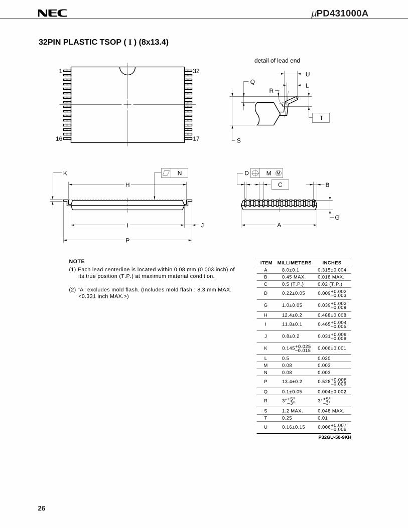
32PIN PLASTIC TSOP ( I ) (8x13.4)
NOTE
(1) Each lead centerline is located within 0.08 mm (0.003 inch) of its true position (T.P.) at maximum material condition.
ITEM MILLIMETERS INCHES
P32GU-50-9JH
B 0.45 MAX. 0.018 MAX.
C 0.5 (T.P.) 0.02 (T.P.)
detail of lead end
A 8.0±0.1 0.315±0.004
H 12.4±0.2 0.488±0.008
B
T
N
D 0.22±0.05 0.009+0.002–0.003
G 1.0±0.05 0.039+0.003–0.009
I 11.8±0.1 0.465+0.004–0.005
J 0.8±0.2 0.031+0.009–0.008
K
L 0.5 0.020
M 0.08 0.003
N 0.08 0.003
Q 0.1±0.05 0.004±0.002
P 13.4±0.2 0.528+0.008–0.009
S 1.2 MAX. 0.048 MAX.
R 3° 3°
T 0.25 0.01
U 0.16±0.15 0.006+0.007–0.006
+5°–3°
+5°–3°
(2) "A" excludes mold flash. (Includes mold flash : 8.3 mm MAX. <0.331 inch MAX.>)
M
U
LR
Q
S
D M
C
G
K
J
1
16
32
17
A
0.145+0.025–0.015 0.006±0.001
H
P
I
26
µPD431000A
32PIN PLASTIC TSOP ( I ) (8x13.4)
NOTE
(1) Each lead centerline is located within 0.08 mm (0.003 inch) of its true position (T.P.) at maximum material condition.
ITEM MILLIMETERS INCHES
P32GU-50-9KH
B 0.45 MAX. 0.018 MAX.
C 0.5 (T.P.) 0.02 (T.P.)
detail of lead end
A 8.0±0.1 0.315±0.004
H 12.4±0.2 0.488±0.008
B
T
N
D 0.22±0.05 0.009+0.002–0.003
G 1.0±0.05 0.039+0.003–0.009
I 11.8±0.1 0.465+0.004–0.005
J 0.8±0.2 0.031+0.009–0.008
K
L 0.5 0.020
M 0.08 0.003
N 0.08 0.003
Q 0.1±0.05 0.004±0.002
P 13.4±0.2 0.528+0.008–0.009
S 1.2 MAX. 0.048 MAX.
R 3° 3°
T 0.25 0.01
U 0.16±0.15 0.006+0.007–0.006
+5°–3°
+5°–3°
(2) "A" excludes mold flash. (Includes mold flash : 8.3 mm MAX. <0.331 inch MAX.>)
1
16
32
17
M
U
LR
Q
S
D M
C
GA
K
J
H
P
I
0.145+0.025–0.015 0.006±0.001

27
µPD431000A
Recommended Soldering ConditionsThe following conditions must be met when soldering conditions of the µPD431000A.
For more details, refer to our document “SEMICONDUCTOR DEVICE MOUNTING TECHNOLOGY MANUAL”
(C10535E).
Please consult with our sales offices in case other soldering process is used, or in case soldering is done
under different conditions.
Types of Surface Mount Device
µPD431000AGW : 32-pin Plastic SOP (525 mil)
µPD431000AGZ-KJH : 32-pin Plastic TSOP(I) (8 × 20 mm) (Normal bent)
µPD431000AGZ-KKH : 32-pin Plastic TSOP(I) (8 × 20 mm) (Reverse bent)
µPD431000AGU-9JH : 32-pin Plastic TSOP(I) (8 × 13.4 mm) (Normal bent)
µPD431000AGU-9KH : 32-pin Plastic TSOP(I) (8 × 13.4 mm) (Reverse bent)
Please consult with our sales offices
Type of Through Hole Mount Device
µPD431000ACZ: 32-pin Plastic DIP (600 mil)
Soldering process Soldering conditions
Wave soldering Solder temperature: 260 °C or below,
(Only to leads) Flow time: 10 seconds or below
Partial heating method Pin temperature: 300 °C or below,
Time: 3 seconds or below (Per one lead)
Caution Do not jet molten solder on the surface of package.
28
µPD431000A
[MEMO]

29
µPD431000A
[MEMO]

30
µPD431000A
[MEMO]

31
µPD431000A
NOTES FOR CMOS DEVICES
1 PRECAUTION AGAINST ESD FOR SEMICONDUCTORS
Note: Strong electric field, when exposed to a MOS device, can cause destruction
of the gate oxide and ultimately degrade the device operation. Steps must
be taken to stop generation of static electricity as much as possible, and
quickly dissipate it once, when it has occurred. Environmental control must
be adequate. When it is dry, humidifier should be used. It is recommended
to avoid using insulators that easily build static electricity. Semiconductor
devices must be stored and transported in an anti-static container, static
shielding bag or conductive material. All test and measurement tools
including work bench and floor should be grounded. The operator should
be grounded using wrist strap. Semiconductor devices must not be touched
with bare hands. Similar precautions need to be taken for PW boards with
semiconductor devices on it.
2 HANDLING OF UNUSED INPUT PINS FOR CMOS
Note: No connection for CMOS device inputs can be cause of malfunction. If no
connection is provided to the input pins, it is possible that an internal input
level may be generated due to noise, etc., hence causing malfunction. CMOS
device behave differently than Bipolar or NMOS devices. Input levels of
CMOS devices must be fixed high or low by using a pull-up or pull-down
circuitry. Each unused pin should be connected to V DD or GND with a
resistor, if it is considered to have a possibility of being an output pin. All
handling related to the unused pins must be judged device by device and
related specifications governing the devices.
3 STATUS BEFORE INITIALIZATION OF MOS DEVICES
Note: Power-on does not necessarily define initial status of MOS device. Produc-
tion process of MOS does not define the initial operation status of the device.
Immediately after the power source is turned ON, the devices with reset
function have not yet been initialized. Hence, power-on does not guarantee
out-pin levels, I/O settings or contents of registers. Device is not initialized
until the reset signal is received. Reset operation must be executed imme-
diately after power-on for devices having reset function.
2
µPD431000A
[MEMO]
No part of this document may be copied or reproduced in any form or by any means without the prior writtenconsent of NEC Corporation. NEC Corporation assumes no responsibility for any errors which may appear inthis document.NEC Corporation does not assume any liability for infringement of patents, copyrights or other intellectual propertyrights of third parties by or arising from use of a device described herein or any other liability arising from useof such device. No license, either express, implied or otherwise, is granted under any patents, copyrights or otherintellectual property rights of NEC Corporation or others.While NEC Corporation has been making continuous effort to enhance the reliability of its semiconductor devices,the possibility of defects cannot be eliminated entirely. To minimize risks of damage or injury to persons orproperty arising from a defect in an NEC semiconductor device, customers must incorporate sufficient safetymeasures in its design, such as redundancy, fire-containment, and anti-failure features.NEC devices are classified into the following three quality grades:"Standard", "Special", and "Specific". The Specific quality grade applies only to devices developed based on acustomer designated "quality assurance program" for a specific application. The recommended applications ofa device depend on its quality grade, as indicated below. Customers must check the quality grade of each devicebefore using it in a particular application.
Standard: Computers, office equipment, communications equipment, test and measurement equipment,audio and visual equipment, home electronic appliances, machine tools, personal electronicequipment and industrial robots
Special: Transportation equipment (automobiles, trains, ships, etc.), traffic control systems, anti-disastersystems, anti-crime systems, safety equipment and medical equipment (not specifically designedfor life support)
Specific: Aircrafts, aerospace equipment, submersible repeaters, nuclear reactor control systems, lifesupport systems or medical equipment for life support, etc.
The quality grade of NEC devices is "Standard" unless otherwise specified in NEC's Data Sheets or Data Books.If customers intend to use NEC devices for applications other than those specified for Standard quality grade,they should contact an NEC sales representative in advance.Anti-radioactive design is not implemented in this product.
M4 96.5