more papers and · pdf file · 2012-03-27use of a mobile phone for robotic control...
TRANSCRIPT

MOBILE OPERATED LAND ROVER
Document BySANTOSH BHARADWAJ REDDYEmail: [email protected]
Engineeringpapers.blogspot.comMore Papers and Presentations available on above site
ABSTRACT
onventionally, Wireless-controlled robots use RF circuits, which have the drawbacks of limited working range, limited frequency range and the limited control. Use of a mobile phone for robotic
control can overcome these limitations. It provides the advantage of robust control, working range as large as the coverage area of the service provider, no interference with other controllers and up to twelve controllers.
C
Although the appearance and the capabilities of robots vary vastly, all robots share the feature of a mechanical, movable structure under some form of control. The Control of robot involves three distinct phases: perception, processing and action. Generally, the preceptors are sensors mounted on the robot, processing is done by the on-board microcontroller or processor, and the task is performed using motors or with some other actuators.
SPECIFICATION
1. Dimensions – 100mm x 150mm (4”x6”)
2. MCU – ATMEL AT89S52 MCU (Microcontroller)
3. Power supply – +5v regulated DC, +12v regulated DC
4. Interface – DTMF HT9170, OPTO-COPULER MCT2E, MOTOR DRIVER L293D
5. Data speed – 57600bps, 8bits
1
6. File format – Intel 8-bit Hex
FEATURES
1. Storing of Standby request after the CALL was disconnected
2. Supports up to 12 operations from the mobile phone
3. This circuit is compatible for any MOBILE
4. Low power consumptions
5. Hibernation
OPERATION
In this project the robot, is controlled by a mobile phone that makes call to the mobile phone attached to the robot in the course of the call, if any button is pressed control corresponding to the button pressed is heard at the other end of the call. This tone is called dual tone multi frequency (DTMF). The robot receives this DTMF tone with the help of phone stacked in the robot. The received tone is processed by the ATMEL AT89S52 microcontroller with the help of DTMF decoder HT9170 the decoder decodes the DTMF tone in to its equivalent binary digit and this binary number is send to the microcontroller, the microcontroller is preprogrammed to take a decision for any give input and outputs its decision to motor drivers in order to drive the motors for forward or backward motion or a turn. The mobile that makes a call to the mobile phone stacked in the robot acts as a remote. So this simple robotic project does not require the construction of receiver and transmitter units. DTMF signaling is used for telephone signaling over the line in the voice-frequency band to the call switching center. The version of DTMF used for telephone dialing is known as touch-tone. DTMF assigns a specific frequency (consisting of two separate tones) to each key so that it can easily be identified by the electronic circuit. The signal generated by the DTMF encoder is the direct algebraic submission, in real time, of the amplitudes of two sine (cosine) waves of different frequencies, i.e., pressing ‘5’ will send a tone made by adding 1336 Hz and 770 Hz to the other end of the mobile. The tones and assignments in a DTMF system shown in Table 1
2
TABLE 1 TONES AND ASSIGNMENTS IN A DTMF SYSTEMFrequencies 1209Hz 1336Hz 1477Hz 1633Hz
697HZ 1 2 3 A770Hz 4 5 6 B852Hz 7 8 9 C941Hz * 0 # D
TABLE 2 DTMF DATA OUTPUTLow Hz High Hz Digit OE D3 D2 D1 D0
697 1209 1 H L L L H697 1336 2 H L L H L697 1477 3 H L L H H770 1209 4 H L H L L770 1336 5 H L H L H770 1477 6 H L H H L852 1209 7 H L H H H852 1336 8 H H L L L852 1477 9 H H L L H941 1336 0 H H L H L941 1209 * H H L H H941 1477 # H H H L L697 1633 A H H H L H770 1633 B H H H H L852 1633 C H H H H H941 1633 D H L L L L-- -- ANY L 0 0 0 0
3

SPARES LIST FOR THE MOBILE OPERATED LAND ROVER
POWER SUPPLY
SL.NO PART ID PART NAME PART VALUE QUANTITY01 R1 RESISTOR 1KE 0102 R2 RESISTOR 470E 0103 C1-C2 CAPACITOR 1000uF/25V 0204 C3-C4 CAPACITOR 0.1uF (104) 0205 BR1 BRIDGE
DIODEW10M 01
06 D1-D2 LED’s 5MM (RED) 0207 RG1 IC
REGULATORGM7812 01
08 RG2 IC REGULATOR
GM7805 01
09 T1 TRANSFORMER
0-12V/500mA
01
10 -- PCB 2” X 3” 0111 -- POWER
CORD2MTRS 01
12 B1 BATTERY 12V 1.3AH 01
MAIN CIRCUIT BOARD
SL.NO PART ID PART NAME PART VALUE QUANTITY01 R1 RESISTOR 10KE 0102 R2 RESISTOR 390KE 01
4

03 R3-R4 RESISTOR 100KE 0204 R5-R9 RESISTOR 470E 0505 R10-R14 RESISTOR 1KE 0506 C1 CAPACITOR 10uF/63V 0107 C2-C3 CAPACITOR 33pF 0208 C4-C6 CAPACITOR 0.1uF (104) 0309 X1 CRYSTAL
OSC3.579545MH
z01
10 X2 CRYSTAL OSC
11.05920MHz
01
11 RP1 SIP-RESISTOR
10KE (103) 01
12 IC1 DTMF IC HT9170 0113 IC2 MCU-52 IC ATMEL
AT89S5201
14 IC3-IC7 OPTO-COPULER
MCT2E 05
15 IC8 MOTOR DRIVER
L293D 01
16 SW1 RESET SWITCH
-- 01
17 -- PCB 4” X 6” 01
ACCESSORIES
SL.NO PART ID PART NAME PART VALUE QUANTITY01 -- FLUX 15GRAMS 0102 -- LEAD 50GRAMS 0103 -- DESOLDER
WICK1.5M, 2.5MM 01
04 -- RIBBON WIRE
5MTRS 01
05 -- NOKIA HEADSET
MODEL 1650 01
06 -- WIRE STRIPPER
-- 01
07 -- WIRE CUTTER
-- 01
08 -- BRUSH ANTI-STATIC 0109 -- SCREW
DRIVERSTAR-BIT 01
10 -- NUT & -- RECOMMEND
5

BOLTS ED
ROBOTICS
SL.NO PART ID PART NAME PART VALUE QUANTITY01 MTR1-MTR2 GEARED
MOTOR12V DC, 60RPM
02
02 -- AXIAL ROD 6 INCH 0103 -- WHEELS -- 0404 -- BODY KIT -- 01
BLOCK DIAGRAM OF MOBILE OPERATED LAND ROVER
6

CIRCUIT DESCRIPTION
Shows block diagram of the MOBILE PHONE OPERATED LAND ROVER. The important components of this rover are a DTMF decoder, microcontroller and motor driver. An HT9170 series DTMF decoder used here. All types of HT9170 series use digital counting techniques to detect and decode all the 16 DTMF tone pairs into a 4-bit code output. The built-in dial tone rejection circuit eliminates the need for pre-filtering. When the input signal given at pin 2(IN-) in single-ended input configuration is recognized to be effective, the correct 4-bit decode signal of the DTMF tone is transferred to Q1 (PIN 11) through Q4 (PIN 14) outputs.
Table 2 shows the DTMF data output table of HT9170. Q1 through Q4 outputs of the DTMF decoder (IC1) are connected to port pins P0.4 through P0.7 of Atmel AT89S52 microcontroller (IC2)
The Atmel AT89S52 is a low-power, 8-bit, CMOS microcontroller based on the Atmel enhanced RISC architecture. It provides the following features: 8kB of in-system programmable Flash program memory with read-while-write
capabilities, 512 bytes of EEPROM ,1 KB SRAM ,32 general purpose working registers .All the 32 registers are directly connected to the arithmetic logic unit, allowing two independent registers to be accessed in one clock cycle. The resulting architecture is code-efficient.
7
Outputs from port pins PDO through PD3 and PD7 of the microcontroller are fed to inputs IN1 through IN4 and enable pins (EN1 andEN2) of motor driver L293D, respectively to drive two geared DC motors. Switch S1 is used for manual reset. The microcontroller output is not sufficient to drive the DC motors, so current drivers are required for motor rotation.
The L293D is a quad, high-current, half-H driver designed to provide bidirectional drive currents of up to 600mA at voltages from 4.5 V to 36V. It makes it easier to drive the DC motors. The L293D consists of four drivers. Pins IN1 through IN4 and OUT1 through OUT4 are input and output pins, respectively , of driver 1 through driver 4 .drivers 1 and 2 ,and drivers 3 and 4 are enabled by enable pin 1 (EN1)and pin9 (EN2) ,respectively .When enable input EN1 (pin1) is high ,drivers 1 and 2 are enabled and the outputs corresponding to their inputs are active. Similarly, enable input EN2 (pin9) enables drivers 3 and 4.
An actual-size, single –side PCB for cell phone – operated land rover is shown in Fig.4 and its component layout in Fig.5.
SOFTWARE DESCRIPTION
The software is written in ‘C’ language and compiled using Code Vision AVR ‘C’ compiler. The source program is converted into hex code by the compiler. Burn this hex code into ATmega16 AVR microcontroller.
The source program is well commented and easy to understand. First include the register name defined specifically for ATmega16 and also declare the variable. Set port A as the input and port D as the output. The program will run forever by using ‘while’ loop. Under ’while’ loop, read port A and test the received input using ‘switch’ statement. The corresponding data will output at port D after testing of the received data.
WORKING
In order to control the robot, you need to make a call to the cell phone attached to the robot(through head phones) from any phone, which sends DTMF tunes on pressing the numeric buttons. The cell phone in the robot is kept in ‘auto answer ’ mode.(if the mobile does not have the auto answering facility, receive the call by ‘OK ’ on the rover-connected mobile and then made it in hands-free mode.)So after a ring, the cell phone accepts the call.
Now you may press any button on your mobile to perform actions as listed in Table3.The DTMF tones thus produced are received by the cell phone in the robot. These tones are fed to the circuit by the headset of the cell phone. The
8

MT8870 decodes the received tone sends the equivalent binary number to the microcontroller .According to the program in the microcontroller, the robot starts moving.
When you press key ‘2’ (binary equivalent 00000010) on your mobile phone, the microcontroller outputs ‘10001001’ binary equivalent. Port pins PD0, PD3 andPD7 are high. The high output at PD7of the microcontroller drives the motor driver (L293D). Port pins PD3 and PD0 drive motors M1 and M2 in forward directions( as per table3) .Similarly ,motors M1 and M2 move for left turn, right turn , backward motion and stop condition as per table3.
CONSTRUCTION
When constructing any robot, one major mechanical constraint is the number of motors being used. You can have either a two-wheel drive or a four-wheel drive. Though four –wheel drive is more complex than the two-wheel drive; it provides more torque and good control. Two wheel drive, on the other hand, is very easy to construct.
Top view of a four-wheel driven land rover is shown in Fig.3.the chassis used in this model is a 10x18c m2 sheet made up of parax. Motors are fixed to the bottom of this sheet and the circuit is affixed firmly on top of the sheet. A cell phone is also mounted on the sheet as shown in the picture.
In the four wheel drive system, the two motors on a side are controlled in parallel. So a single L239D driver IC can drive the rover. For this robot, beads affixed with glue act as support wheels.
FURTHER APPLICATIONS
This land rover can be further improved to serve specific purposes. It requires four controls to roam around. The remaining eight controls can be configured to serve other purposes, with some modifications in the source program of the microcontroller.
9

NOKIA 1650 MOBILE – For receiving the IF signals (Intermediate Frequency) from any mobile we used a NOKIA 1650 mobile phone instead of GSM module.
NOKIA STEREO HEADSET HS-47
10

NOKIA 1650
11

HT9170 DTMF Receiver
FEATURES
1. Operating voltage: 2.5V~5.5V
2. Minimal external components
3. No external filter is required
4. Low standby current (on power down mode)
5. Excellent performance
6. Tristate data output for µC interface
7. 3.58MHz crystal or ceramic resonator
8. 1633Hz can be inhibited by the INH pin
9. HT9170B: 18-pin DIP package
HT9170D: 18-pin SOP package
10.Complete DTMF Receiver
11.Low power consumption
12.Internal gain setting amplifier
13.Adjustable guard time
14.Central office quality
15.Power-down mode
16.Inhibit mode
DESCRIPTION
The HT9170 series are Dual Tone Multi Frequency (DTMF) receivers integrated with digital decoder and bandsplit filter functions. The HT9170B and HT9170D types supply power-down mode and inhibit mode operations. All types of theHT9170 series use digital counting techniques to detect and decode all the 16 DTMF tone pairs into a 4-bit code output. Highly accurate
12
switched capacitor filters are employed to divide tone (DTMF) signals into low and high group signals. A built-in dial tone rejection circuit is provided to eliminate the need for pre-filtering.
APPLICATIONS
1. Receiver system for British Telecom (BT) or CEPT Spec (HT9170B HT9170D)
2. Paging systems
3. Repeater systems/mobile radio
4. Credit card systems
5. Remote control
6. Personal computers
7. Telephone answering machine
BLOCK DIAGRAM
13

DTMF DIALING MATRIX
14

PIN DESCRIPTION
PIN # NAME DESCRIPTION18
20
1 1 IN+ Non – Inverting Op – Amp (Input)2 2 IN- Inverting Op – Amp (Input)3 3 GS Gain Select. Gives access to output of front end
differential amplifier for connection of Feedback resistor
4 4 VRef Reference Voltage (Output). Nominally VDD/2 is used to bias inputs at mid-rail
5 5 INH Inhibit (Input). Logic high inhibits the detection of tones representing characters A, B, C and D. This pin
input is internally pulled down6 6 PWDN Power Down (Input). Active high. Powers down the
device and inhibits the oscillator. This pin input is
15

internally pulled down7 8 OSC1 Clock (Input)8 9 OSC2 Clock (Output). A 3.579545 MHz crystal connected
between pins OSC1 and OSC2 completes the internal oscillator circuit
9 10 Vss Ground (Input). 0V typical10
11 TOE Three State Output Enable (Input). Logic high enables the outputs Q1-Q4. This pin is pulled up internally
11 - 14
12 -
15
Q1-Q4 Three State Data (Output). When enabled by TOE, provide the code corresponding to the 14 15 last valid
tone-pair received. When TOE is logic low, the data outputs are high impedance.
15
17 StD Delayed Steering (Output).Presents a logic high when a received tone-pair has been registered and the
output latch updated; returns to logic low when the voltage on St/GT falls below VTSt
16
18 ESt Early Steering (Output). Presents logic high once the digital algorithm has detected a valid tone pair (signal condition). Any momentary loss of signal condition will
cause ESt to return to a logic low17
19 St/GT Steering Input/Guard time (Output) Bidirectional. A voltage greater than VTSt detected at St causes the
device to register the detected tone pair and update the output latch. A voltage less than VTSt frees the
device to accept a new tone pair. The GT output acts to reset the external steering time-constant; its state is
a function of ESt and the voltage on St18
20 VDD Positive power supply (Input). +5V typical
7, 16
NC No Connection
FUNCTIONAL DESCRIPTION
The HT9170 series tone decoders consist of three band pass filters and two digital decode circuits to convert a tone (DTMF) signal into digital code output.
16
FILTER SECTION
The pre-filter is a band rejection filter which reduces the dialing tone from 350Hz to 400Hz. The low group filter filters low group frequency signal output whereas the high group filter filters high group frequency signal output. Each filter output is followed by a zero-crossing detector with hysteresis. When each signal amplitude at the output exceeds the specified level, it is transferred to full swing logic signal. When input signals are recognized to be effective, DV becomes high, and the correct tone code (DTMF) digit is transferred.
DECODER SECTION
Following the filter section is a decoder employing digital counting techniques to determine the frequencies of the incoming tones and to verify that they correspond to standard DTMF frequencies. A complex averaging algorithm protects against tone simulation by extraneous signals such as voice while providing tolerance to small frequency deviations and variations. This averaging algorithm has been developed to ensure an optimum combination of immunity to talk-off and tolerance to the presence of interfering frequencies (third tones) and noise. When the detector recognizes the presence of two valid tones (this is referred to as the “signal condition” in some industry specifications) the “Early Steering” (EST) output will go to an active state. Any subsequent loss of signal condition will cause EST to assume an inactive state.
STEERING CIRCUIT
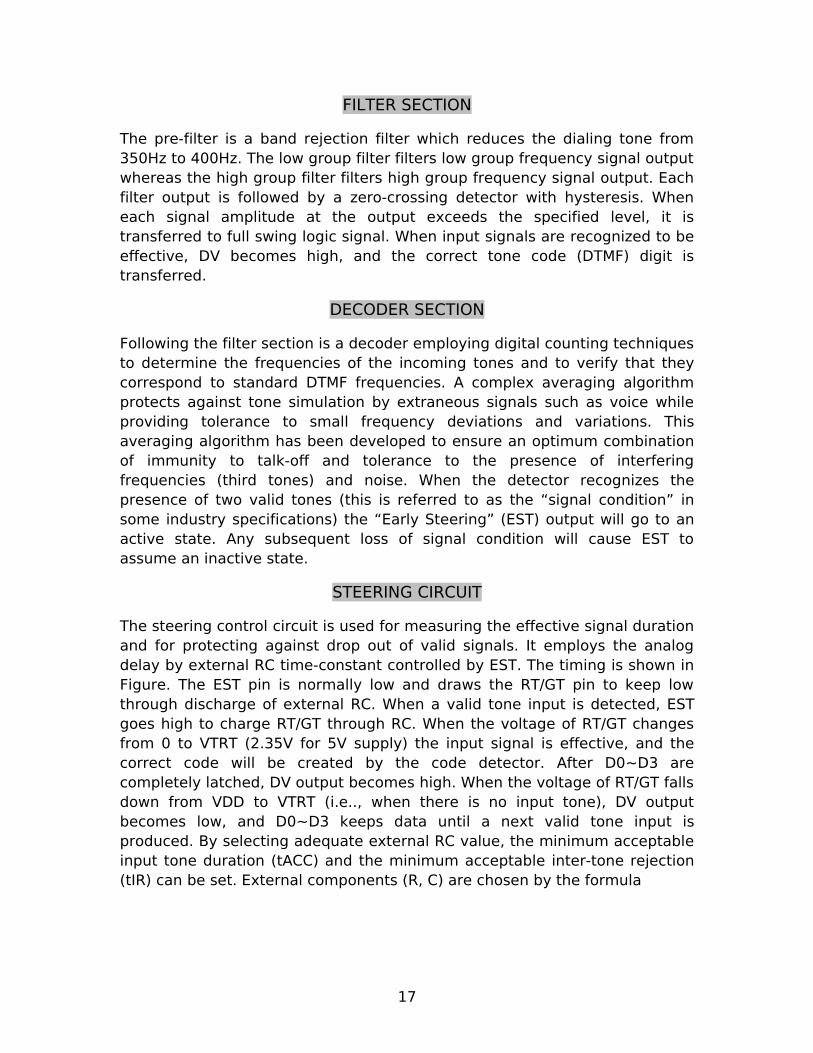
The steering control circuit is used for measuring the effective signal duration and for protecting against drop out of valid signals. It employs the analog delay by external RC time-constant controlled by EST. The timing is shown in Figure. The EST pin is normally low and draws the RT/GT pin to keep low through discharge of external RC. When a valid tone input is detected, EST goes high to charge RT/GT through RC. When the voltage of RT/GT changes from 0 to VTRT (2.35V for 5V supply) the input signal is effective, and the correct code will be created by the code detector. After D0~D3 are completely latched, DV output becomes high. When the voltage of RT/GT falls down from VDD to VTRT (i.e.., when there is no input tone), DV output becomes low, and D0~D3 keeps data until a next valid tone input is produced. By selecting adequate external RC value, the minimum acceptable input tone duration (tACC) and the minimum acceptable inter-tone rejection (tIR) can be set. External components (R, C) are chosen by the formula
17
STEERING TIME ADJUSTMENT CIRCUITS
POWER-DOWN AND INHIBIT MODE
A Logic high applied to pin 6 (PWDN) will power down the device to minimize the power consumption in a standby mode. It stops the oscillator and the functions of the filters. Inhibit mode is enabled by a logic high input to the pin 5 (INH). It inhibits the detection of tones representing characters A, B, C, and D. The output code will remain the same as the previous detected code
18

DIFFERENTIAL INPUT CONFIGURATION
The input arrangement of the HT9170B/HT9170D provides a differential-input operational amplifier as well as a bias source (VRef) which is used to bias the inputs at mid-rail. Provision is made for connection of a feedback resistor to the op-amp output (GS) for adjustment of gain. In a single-ended configuration, the input pins are connected as shown in Figure with the op-amp connected for unity gain and VRef biasing the input at 1/2 VDD. Figure shows the differential configuration, which permits the adjustment of gain with the feedback resistor R5.
19

CRYSTAL OSCILLATOR
The internal clock circuit is completed with the addition of an external 3.579545 MHz crystal and is normally connected as shown in Figure (Single-Ended Input Configuration). However, it is possible to configure several MT8870D/MT8870D-1 devices employing only a single oscillator crystal. The oscillator output of the first device in the chain is coupled through a 30 pF capacitor to the oscillator input (OSC1) of the next device. Subsequent devices are connected in a similar fashion. The problems associated with unbalanced loading are not a concern with the arrangement shown, i.e., precision balancing capacitors are not required.
APPLICATION CIRCUIT
20

MICROCONTROLLER
1.1WHAT ARE MICROCONTROLLERS AND WHAT ARE THEY USED FOR?
As all other good things, this powerful component is basically very simple and is obtained by uniting tested and high- quality "ingredients" (components) as per following receipt:
1. The simplest computer’s processor is used as a "brain" of the future system.
21

2. Depending on the taste of the producer, it is added: a bit of memory, a few A/D converters, timers, input/output lines etc.
3. It is all placed in one of standard packages.
4. Simple software that will be able to control it all and about which everyone will be able to learn has been developed.
Three things have had a crucial impact on such a success of the microcontrollers:
1. Powerful and intelligently chosen electronics embedded in the microcontrollers can via input/output devices (switches, push buttons, sensors, LCD displays, relays…) control various processes and devices such as: industrial automatics, electric current, temperature, engine performance etc.
2. A very low price enables them to be embedded in such devices in which, until recent time it was not worth embedding anything. Thanks to that, the world is overwhelmed today with cheap automatic devices and various “intelligent” appliances.
3. Prior knowledge is hardly needed for programming. It is sufficient to have any kind of PC (software in use is not demanding at all and it is easy to learn to work on it) and one simple device (programmer) used for “transferring” completed programs into the microcontroller.
Therefore, if you are infected with a virus called electronics, there is nothing left for you to do but to learn how to control its power and how to direct it at the right course?
SPECIAL INTERFACES IN MICROCONTROLLERS:
22

PROGRAM MEMORY (ROM)
The Program Memory is a type of memory which permanently stores a program being executed. Obviously, the maximal length of the program that can be written to depends on the size of the memory. Program memory can be built in the microcontroller or added from outside as a separate chip, which depends on type of the microcontroller. Both variants have advantages and disadvantages: if added from outside, the microcontroller is cheaper and program can be considerably longer. At the same time, a number of available pins are decremented as the microcontroller uses its own input/output ports to be connected to the memory. The capacity of Internal Program Memory is usually smaller and more expensive but such a chip has more possibilities of connecting to peripheral environment. Program memory size ranges from 512B to 64KB.
DATA MEMORY (RAM)
Data Memory is a type of memory used for temporary storing and keeping different data and constants created and used during operating process. The content of this memory is erased once the power is off. For example: when the program performs addition, it is necessary to have a register presenting what in everyday life is called “a sum”. For that purpose one of the registers in RAM is named as such and serves for storing results of addition. Data memory size goes up to a few KBs.
EEPROM MEMORY
The EEPROM Memory is a special type of memory which not all the types of the microcontrollers have. Its content can be changed during program execution (similar to RAM), but it is permanently saved even after the power goes off (similar to ROM). It is used for storing different values created and used during operating process and which must be saved upon turning off the device (calibration values, codes, values to count up to etc.). A disadvantage of this memory is that programming is relatively slow- measured in milliseconds.
23

SFRS (Special Function Registers)
SFRs are a particular part of memory whose purpose is defined in advance by the producer. Each of these registers has its name and controls some of interfaces within the microcontroller. For example: by writing zero or one to the SFR controlling some input/output port, each of the port pins can be configured as input or output (each bit in this register controls the purpose of one single pin).
24
CPU (CENTRAL PROCESSOR UNIT)
As its name tells, this is "Big Brother" who monitors and controls all operations being performed within the microcontroller and the user cannot affect its work. It consists of several smaller units. The most important are:
1. Instruction decoder - a part of electronics which recognizes program instructions and on the basis of which runs other circuits.
2. Arithmetical Logical Unit (ALU) - performs all mathematical and logical operations with data. The features of this circuit are described in the "instruction set" which differs for each type of the microcontroller.
3. Accumulator - is a special type of the SFR closely related to operating mode of the ALU It is a kind of desk on which all data needed to perform some operation on are set (addition, shift etc.). It also contains a result, ready to be used further in operation. One of the SFRs, called the Status Register, is closely related to the accumulator, showing at any time the "status" of a number being in the accumulator (the number is greater than or less than zero etc.).
INPUT/OUTPUT PORTS (I/O PORTS)
The microcontroller cannot be of any use without being connected to peripheral devices. For that reason each microcontroller has one or more registers connected to its pins (called ports in this case).
Why input/output? Because the user can change pin’s role according to his/her own needs. These are, in fact, the only registers in the microcontroller whose state can be checked by voltmeter.
25

OSCILLATOR
The oscillator can be compared with rhythm section of a mini orchestra. Equalized pulses coming from this circuit enable harmonious and synchronic operating of all other parts of the microcontroller. It is commonly configured so as to use quartz-crystal or ceramics resonator for frequency stabilization. Besides, it can often operate without elements for frequency stabilization (like RC oscillator). It is important to know that instructions are not executed at the rate ordered by oscillator but several times slower. The reason for this is that each instruction is executed in several steps (In some microcontrollers execution time of all instructions is equal, while in others microcontroller’s execution time differs for different instructions). Consequently, if your system uses quartz-crystal of 20MHz, execution time of a program instruction is not 50noS but 200, 400 or even 800 noS.
26

TIMERS/COUNTERS
Most programs use in some way these miniature electronic "stopwatches". They are mostly 8- or 16-bit SFRs whose value is automatically incremented with each coming pulse. Once the register is completely "filled up"- an interrupt is generated!
If the registers use internal oscillator for its operating then it is possible to measure the time between two events ( if the register value is T1 at the moment measuring has started, and T2 at the moment measuring has finished, then the time that has passed is equal to the value gained by their subtraction T2-T1 ). If the registers for its operating use pulses coming from external source then such a timer is converted to counter.
This is a very simple explanation used to describe the essence of the operating. It’s a bit more complicatedinpractice.
27

WATCHDOG TIMER
Its name tells a lot about its purpose. Watchdog Timer is a timer connected to a particular and totally independent RC oscillator within the microcontroller.
If enabled to operate, every time it "counts up to end", the microcontroller is reset and program execution starts from the first instruction. To keep this from happening by using particular command, the whole idea is based on the fact that every program circulates, in other words, the program is executed in several longer or shorter loops.
If the instruction which resets the value of the watchdog timer is set at some important program locations, besides commands being regularly executed, then the operation of the watchdog timer will not be noticed.
If for any reason (usually electrical disturbances in industry), the program counter "gets stuck" at memory location from where there is no return, the register’s value being steadily incremented by the watchdog timer will reach the maximum ET voila! Reset occurs!
28

SERIAL COMMUNICATION
Connection between the microcontroller and peripheral devices established through I/O ports is an ideal solution for shorter distances- up to several meters. But, when it is needed to enable communication between two devices on longer distances or when for any other reason it is not possible to use "parallel" connection (for example remote control of the aircraft) it is obvious that something so simple cannot be taken into account. In such and similar situations, communication through pulses, called serial communication is the most appropriate to use.
Serial communication problem has been resolved a long time ago and nowadays several different systems enabling this kind of connection are embedded as standard equipment into most microcontrollers. Which of them will be used in very situation depends on several factors. The most important are the following:
1. With how many devices the microcontroller must exchange data?
2. How fast the serial communication must be?
3. What is the distance between devices?
4. Is there any need to transmit and receive data simultaneously?
One of the most important things concerning the use of serial communication is to strictly observe the Protocol. It is a set of rules which must be applied in order to enable devices to recognize the data being exchanged. Fortunately, the microcontrollers automatically take care of it, which leads to a reduction of the programmer’s work to simple writing and reading data.
29

PROGRAM
Unlike other integrated circuits which only need to be connected to other components and then powered on, the microcontrollers need to be programmed too prior to turning the power on. This is so called "a bitter pill" and the main reason why hardware-oriented electronics engineers mainly avoid the microcontrollers. It is a trap causing huge losses because the microcontrollers programming is in fact very simple.
In order to write a program for running microcontrollers, several "low-level" program languages for programming computers can be used – Assembler , C and Basic ( and their versions ). Besides, writing program procedure consists of simple giving instructions in order in which they should be executed. There are also many programs operating in Windows environment used to facilitate work and provide additional- visual tools.
The use of Assembler is described in this book because it is the simplest language with the fastest execution allowing entire control on what is going on in the circuit.
30
ATMEL AT89S52 MICROCONTROLLER
MICROCONTROLLER ATMEL AT89S52
DESCRIPTION – The AT89S52 is a low-power, high-performance CMOS 8-bit microcontroller with 8K bytes of in-system programmable Flash memory. The device is manufactured using Atmel’s high-density nonvolatile memory technology and is compatible with the industry-standard 80C51 instruction set and pinout. The on-chip Flash allows the program memory to be reprogrammed in-system or by a conventional nonvolatile memory programmer. By combining a versatile 8-bit CPU with in-system programmable Flash on a monolithic chip, the Atmel AT89S52 is a powerful microcontroller which provides a highly-flexible and cost-effective solution to many embedded control applications. The AT89S52 provides the following standard features: 8K bytes of Flash, 256 bytes of RAM, 32 I/O lines, Watchdog timer, two data pointers, three 16-bit timer/counters, a six-vector two-level interrupt architecture, a full duplex serial port, on-chip oscillator, and clock circuitry. In addition, the AT89S52 is designed with static logic for operation down to zero frequency and supports two software selectable power saving modes. The Idle Mode stops the CPU while allowing the RAM, timer/counters, serial port, and interrupt system to continue functioning. The Power-down mode saves the RAM contents but freezes the oscillator, disabling all other chip functions until the next interrupt or hardware reset.
31

FEATURES
1. Compatible with MCS-51 Products
2. 8K Bytes of In-System Programmable (ISP) Flash Memory– Endurance: 1000 Write/Erase Cycles
3. 4.0V to 5.5V Operating Range
4. Fully Static Operation: 0 Hz to 33 MHz
5. Three-level Program Memory Lock
6. 256 x 8-bit Internal RAM
7. 32 Programmable I/O Lines
8. Three 16-bit Timer/Counters
9. Eight Interrupt Sources
10.Full Duplex UART Serial Channel
11.Low-power Idle and Power-down Modes
12.Interrupt Recovery from Power-down Mode
13.Watchdog Timer
14.Dual Data Pointer
15.Power-off Flag
A micro-controller can be compared to a small stand alone computer; it is a very powerful device, which is capable of executing a series of pre-programmed tasks and interacting with other hardware devices. Being packed in a tiny integrated circuit (IC) whose size and weight is usually negligible, it is becoming the perfect controller for robots or any machines requiring some kind of intelligent automation. A single microcontroller can be sufficient to control a small mobile robot, an automatic washer machine or a security system. Any microcontroller contains a memory to store the program to be executed, and a number of
32
input/output lines that can be used to interact with other devices, like reading the state of a sensor or controlling a motor.
Nowadays, microcontrollers are so cheap and easily available that it is common to use them instead of simple logic circuits like counters for the sole purpose of gaining some design flexibility and saving some space. Some machines and robots will even rely on a multitude of microcontrollers, each one dedicated to a certain task. Most recent microcontrollers are 'In System Programmable', meaning that you can modify the program being executed, without removing the microcontroller from its place.
Today, microcontrollers are an indispensable tool for the robotics hobbyist as well as for the engineer. Starting in this field can be a little difficult, because you usually can't understand how everything works inside that integrated circuit, so you have to study the system gradually, a small part at a time, until you can figure out the whole image and understand how the system works.
BLOCK DIAGRAM
33

PIN DIAGRAM
34

PIN DESCRIPTION
35
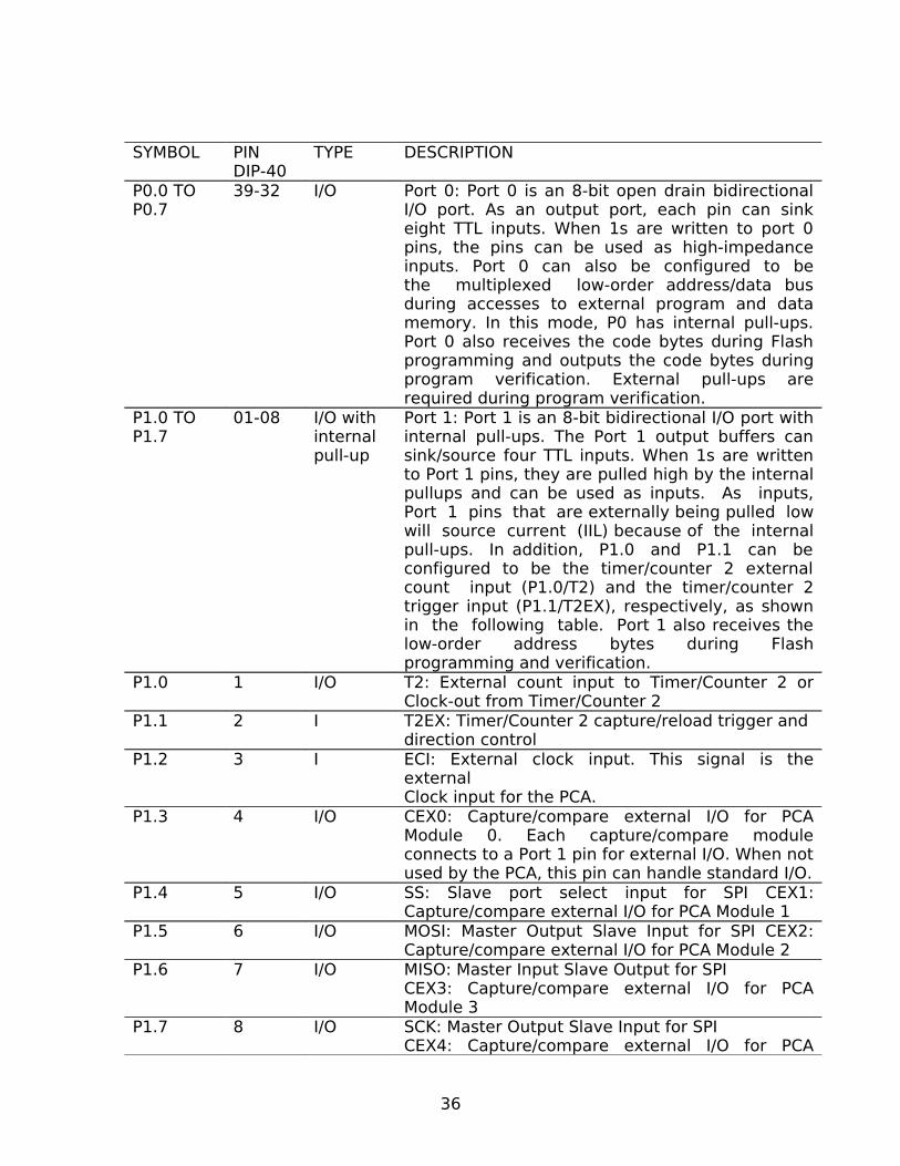
SYMBOL PIN DIP-40
TYPE DESCRIPTION
P0.0 TO P0.7
39-32 I/O Port 0: Port 0 is an 8-bit open drain bidirectional I/O port. As an output port, each pin can sink eight TTL inputs. When 1s are written to port 0 pins, the pins can be used as high-impedance inputs. Port 0 can also be configured to be the multiplexed low-order address/data bus during accesses to external program and data memory. In this mode, P0 has internal pull-ups. Port 0 also receives the code bytes during Flash programming and outputs the code bytes during program verification. External pull-ups are required during program verification.
P1.0 TO P1.7
01-08 I/O withinternal pull-up
Port 1: Port 1 is an 8-bit bidirectional I/O port with internal pull-ups. The Port 1 output buffers can sink/source four TTL inputs. When 1s are written to Port 1 pins, they are pulled high by the internal pullups and can be used as inputs. As inputs, Port 1 pins that are externally being pulled low will source current (IIL) because of the internal pull-ups. In addition, P1.0 and P1.1 can be configured to be the timer/counter 2 external count input (P1.0/T2) and the timer/counter 2 trigger input (P1.1/T2EX), respectively, as shown in the following table. Port 1 also receives the low-order address bytes during Flash programming and verification.
P1.0 1 I/O T2: External count input to Timer/Counter 2 or Clock-out from Timer/Counter 2
P1.1 2 I T2EX: Timer/Counter 2 capture/reload trigger anddirection control
P1.2 3 I ECI: External clock input. This signal is the externalClock input for the PCA.
P1.3 4 I/O CEX0: Capture/compare external I/O for PCA Module 0. Each capture/compare module connects to a Port 1 pin for external I/O. When not used by the PCA, this pin can handle standard I/O.
P1.4 5 I/O SS: Slave port select input for SPI CEX1: Capture/compare external I/O for PCA Module 1
P1.5 6 I/O MOSI: Master Output Slave Input for SPI CEX2: Capture/compare external I/O for PCA Module 2
P1.6 7 I/O MISO: Master Input Slave Output for SPI CEX3: Capture/compare external I/O for PCA Module 3
P1.7 8 I/O SCK: Master Output Slave Input for SPI CEX4: Capture/compare external I/O for PCA
36

Module 4P2.0 TO P2.7
21-28 I/Owith internalpull-up
Port 2: Port 2 is an 8-bit bi-directional I/O port with Internal pull-ups. Port 2 pins are pulled HIGH by the Internal pull-ups when ‘1’s are written to them and can be used as inputs in this state. As inputs, Port 2 pins that are externally pulled LOW will source current (IIL) because of the internal pull-ups. Port 2 sends the high-order address byte during fetches from external program memory and during accesses to external Data Memory that use 16-bit address (MOVX@DPTR). In this application, it uses strong internal pull-ups when transitioning to ‘1’s. Port 2 also receives some control signals and a partial of high-order address bits during the external host mode programming and verification.
P3.0 TO P3.7
10-17 I/Owith internalpull-up
Port 3: Port 3 is an 8-bit bidirectional I/O port with internal pull-ups. Port 3 pins are pulled HIGH by the internal pull-ups when ‘1’s are written to them and can be used as inputs in this state. As inputs, Port 3 pins that are externally pulled LOW will source current (IIL) because of the internal pull-ups. Port 3 also receives some control signals and a partial of high-order address bits during the external host mode programming and verification.
P3.0 10 I RXD: serial input portP3.1 11 O TXD: serial output portP3.2 12 I INT0: external interrupt 0 inputP3.3 13 I INT1: external interrupt 1 inputP3.4 14 I T0: external count input to Timer/Counter 0P3.5 15 I T1: external count input to Timer/Counter 1P3.6 16 O WR: external data memory write strobeP3.7 17 O RD: external data memory read strobePSEN 29 I/O Program Store Enable: PSEN is the read strobe for
external program memory. When the device is executing from internal program memory, PSEN is inactive (HIGH). When the device is executing code from external program memory, PSEN is activated twice each machine cycle, except that two PSEN activations are skipped during each access to external data memory. A forced HIGH-to-LOW input transition on the PSEN pin while the RST input is continually held HIGH for more than 10 machine cycles will cause the device to enter external host mode programming.
37
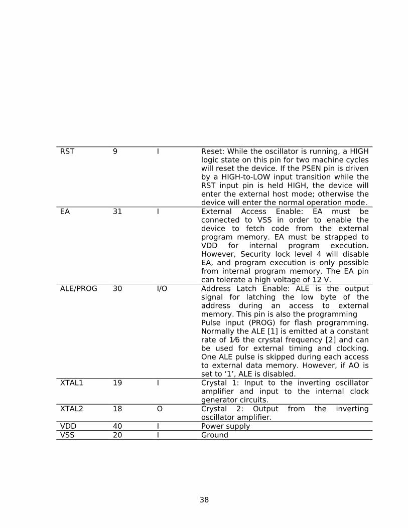
RST 9 I Reset: While the oscillator is running, a HIGH logic state on this pin for two machine cycles will reset the device. If the PSEN pin is driven by a HIGH-to-LOW input transition while the RST input pin is held HIGH, the device will enter the external host mode; otherwise the device will enter the normal operation mode.
EA 31 I External Access Enable: EA must be connected to VSS in order to enable the device to fetch code from the external program memory. EA must be strapped to VDD for internal program execution. However, Security lock level 4 will disable EA, and program execution is only possible from internal program memory. The EA pin can tolerate a high voltage of 12 V.
ALE/PROG 30 I/O Address Latch Enable: ALE is the output signal for latching the low byte of the address during an access to external memory. This pin is also the programmingPulse input (PROG) for flash programming. Normally the ALE [1] is emitted at a constant rate of 1⁄6 the crystal frequency [2] and can be used for external timing and clocking. One ALE pulse is skipped during each access to external data memory. However, if AO is set to ‘1’, ALE is disabled.
XTAL1 19 I Crystal 1: Input to the inverting oscillator amplifier and input to the internal clock generator circuits.
XTAL2 18 O Crystal 2: Output from the inverting oscillator amplifier.
VDD 40 I Power supplyVSS 20 I Ground
38

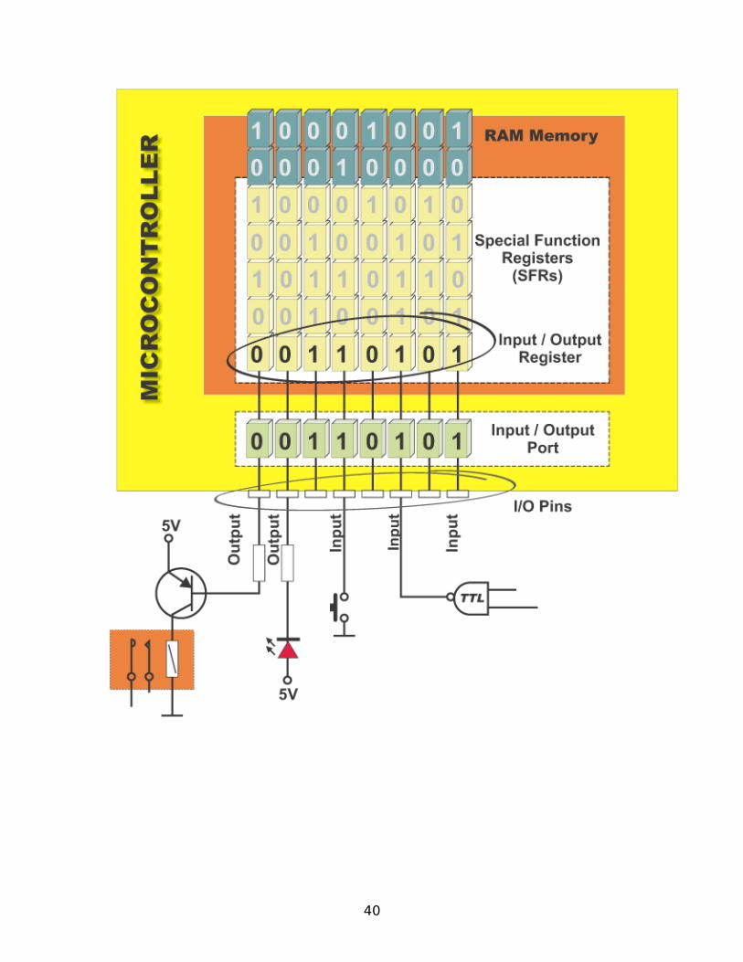
INPUT/OUTPUT PORTS (I/O PORTS)
All 8051 microcontrollers have 4 I/O ports, each consisting of 8 bits which can be configured as inputs or outputs. This means that the user has on disposal in total of 32 input/output lines connecting the microcontroller to peripheral devices.
A logic state on a pin determines whether it is configured as input or output: 0=output, 1=input. If a pin on the microcontroller needs to be configured as output, then logic zero (0) should be applied to the appropriate bit on I/O port. In this way, a voltage level on the appropriate pin will be 0.
Similar to that, if a pin needs to be configured as input, then a logic one (1) should be applied to the appropriate port. In this way, as a side effect a voltage level on the appropriate pin will be 5V (as it is case with any TTL input). This may sound a bit confusing but everything becomes clear after studying a simplified electronic circuit connected to one I/O pin.
39
40
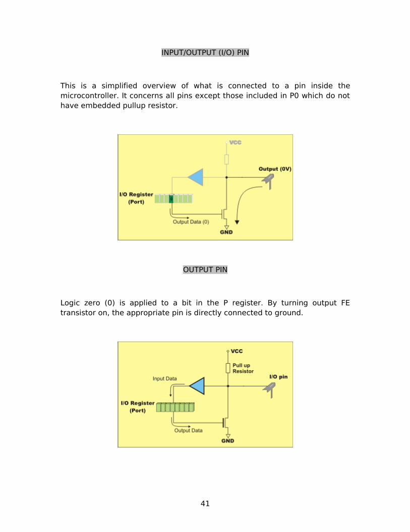
INPUT/OUTPUT (I/O) PIN
This is a simplified overview of what is connected to a pin inside the microcontroller. It concerns all pins except those included in P0 which do not have embedded pullup resistor.
OUTPUT PIN
Logic zero (0) is applied to a bit in the P register. By turning output FE transistor on, the appropriate pin is directly connected to ground.
41

INPUT PIN
Logic one (1) is applied to a bit in the P register. Output FE transistor is turned off. The appropriate pin remains connected to voltage power supply through a pull-up resistor of high resistance.
PORT 0
It is specific to this port to have a double purpose. If external memory is used then the lower address byte (addresses A0-A7) is applied on it. Otherwise, all bits on this port are configured as inputs or outputs.
Another characteristic is expressed when it is configured as output. Namely, unlike other ports consisting of pins with embedded pull-up resistor (connected by its end to 5 V power supply), this resistor is left out here. This, apparently little change has its consequences:
If any pin on this port is configured as input then it performs as if it “floats”. Such input has unlimited input resistance and has no voltage coming from “inside”.
42

When the pin is configured as output, it performs as “open drain”, meaning that by writing 0 to some port’s bit, the appropriate pin will be connected to ground (0V). By writing 1, the external output will keep on “floating”. In order to apply 1 (5V) on this output, an external pull-up resistor must be embedded.
PORT 1
This is a true I/O port, because there are no role assigning as it is the case with P0. Since it has embedded pull-up resistors it is completely compatible with TTL circuits.
PORT 2
Similar to P0, when using external memory, lines on this port occupy addresses intended for external memory chip. This time it is the higher address byte with addresses A8-A15. When there is no additional memory,
43
this port can be used as universal input-output port similar by its features to the port 1.
PORT 3
Even though all pins on this port can be used as universal I/O port, they also have an alternative function. Since each of these functions use inputs, then the appropriate pins have to be configured like that. In other words, prior to using some of reserve port functions, a logical one (1) must be written to the appropriate bit in the P3 register. From hardware’s perspective, this port is also similar to P0, with the difference that its outputs have a pull-up resistor embedded.
CURRENT LIMITATIONS ON PINS
When configured as outputs (logic zero (0)), single port pins can "receive" current of 10mA. If all 8 bits on a port are active, total current must be limited to 15mA (port P0: 26mA). If all ports (32 bits) are active, total maximal current must be limited to 71mA. When configured as inputs (logic 1), embedded pull-up resistor provides very weak current, but strong enough to activate up to 4 TTL inputs from LS series.
SFRS (SPECIAL FUNCTION REGISTERS)
SFRs are a kind of control table used for running and monitoring microcontroller’s operating. Each of these registers, even each bit they include, has its name, address in the scope of RAM and clearly defined purpose ( for example: timer control, interrupt, serial connection etc.). Even though there are 128 free memory locations intended for their storage, the basic core, shared by all types of 8051 controllers, has only 21 such registers. Rests of locations are intentionally left free in order to enable the producers to further improved models keeping at the same time compatibility with the previous versions. It also enables the use of programs written a long time ago for the microcontrollers which are out of production now.
44

A REGISTER (ACCUMULATOR)
This is a general-purpose register which serves for storing intermediate results during operating. A number (an operand) should be added to the accumulator prior to execute an instruction upon it. Once an arithmetical operation is preformed by the ALU, the result is placed into the accumulator. If a data should be transferred from one register to another, it must go through accumulator. For such universal purpose, this is the most commonly used register that none microcontroller can be imagined without (more than a half 8051 microcontroller's instructions used use the accumulator in some way).
B REGISTER
B register is used during multiply and divide operations which can be performed only upon numbers stored in the A and B registers. All other instructions in the program can use this register as a spare accumulator (A).
45

R REGISTERS (R0-R7)
This is a common name for the total 8 general purpose registers (R0, R1, and R2 ...R7). Even they are not true SFRs; they deserve to be discussed here because of their purpose. The bank is active when the R registers it includes are in use. Similar to the accumulator, they are used for temporary storing variables and intermediate results. Which of the banks will be active depends on two bits included in the PSW Register. These registers are stored in four banks in the scope of RAM.
The following example best illustrates the useful purpose of these registers. Suppose that mathematical operations on numbers previously stored in the R registers should be performed: (R1+R2) - (R3+R4). Obviously, a register for temporary storing results of addition is needed. Everything is quite simple and the program is as follows:
MOV A, R3; Means: move number from R3 into accumulator
ADD A, R4; Means: add number from R4 to accumulator (result remains in accumulator)
46

MOV R5, A; means: temporarily moves the result from accumulator into R5
MOV A, R1; Means: move number from R1 into accumulator
ADD A, R2; means: add number from R2 to accumulator
SUBB A, R5; Means: subtract number from R5 (there are R3+R4)
PSW Register (Program Status Word)
This is one of the most important SFRs. The Program Status Word (PSW) contains several status bits that reflect the current state of the CPU. This register contains: Carry bit, Auxiliary Carry, two register bank select bits, Overflow flag, parity bit, and user-definable status flag. The ALU automatically changes some of register’s bits, which is usually used in regulation of the program performing.
P - Parity bit. If a number in accumulator is even then this bit will be automatically set (1), otherwise it will be cleared (0). It is mainly used during data transmission and receiving via serial communication.
Bit 1. This bit is intended for the future versions of the microcontrollers, so it is not supposed to be here.
OV Overflow occurs when the result of arithmetical operation is greater than 255 (decimal), so that it can not be stored in one register. In that case, this bit will be set (1). If there is no overflow, this bit will be cleared (0).
RS0, RS1 - Register bank select bits. These two bits are used to select one of the four register banks in RAM. By writing zeroes and ones to these bits, a group of registers R0-R7 is stored in one of four banks in RAM.
47

RS1 RS2 Space in RAM
0 0 Bank0 00h-07h
0 1 Bank1 08h-0Fh
1 0 Bank2 10h-17h
1 1 Bank3 18h-1Fh
F0 - Flag 0. This is a general-purpose bit available to the user.
AC - Auxiliary Carry Flag is used for BCD operations only.
CY - Carry Flag is the (ninth) auxiliary bit used for all arithmetical operations and shift instructions.
DPTR Register (Data Pointer)
These registers are not true ones because they do not physically exist. They consist of two separate registers: DPH (Data Pointer High) and (Data Pointer Low). Their 16 bits are used for external memory addressing. They may be handled as a 16-bit register or as two independent 8-bit registers. Besides the DPTR Register is usually used for storing data and intermediate results which have nothing to do with memory locations.
48

SP Register (Stack Pointer)
A value of the Stack Pointer ensures that the Stack Pointer will point to valid RAM and permits Stack availability. By starting each subprogram, the value in the Stack Pointer is incremented by 1. In the same manner, by ending subprogram, this value is decremented by 1. After any reset, the value 7 is written to the Stack Pointer, which means that the space of RAM reserved for the Stack starts from this location. If another value is written to this register then the entire Stack is moved to a new location in the memory.
P0, P1, P2, P3 - Input/output Registers
In case that external memory and serial communication system are not in use then, 4 ports with in total of 32 input-output lines are available to the user for connection to peripheral environment. Each bit inside these ports corresponds to the appropriate pin on the microcontroller. This means that
49
logic state written to these ports appears as a voltage on the pin (0 or 5 V). Naturally, while reading, the opposite occurs – voltage on some input pins is reflected in the appropriate port bit.
The state of a port bit, besides being reflected in the pin, determines at the same time whether it will be configured as input or output. If a bit is cleared (0), the pin will be configured as output. In the same manner, if a bit is set to 1 the pin will be configured as input. After reset, as well as when turning the microcontroller on, all bits on these ports are set to one (1). This means that the appropriate pins will be configured as inputs
COUNTERS AND TIMER
As explained in the previous chapter, the main oscillator of the microcontroller uses quartz crystal for its operating. As the frequency of this oscillator is precisely defined and very stable, these pulses are the most suitable for time measuring (such oscillators are used in quartz clocks as well). In order to measure time between two events it is only needed to count up pulses from this oscillator. That is exactly what the timer is doing. Namely, if the timer is properly programmed, the value written to the timer register will be incremented or decremented after each coming pulse, i.e. once per each machine cycle. Taking into account that one instruction lasts 12 quartz oscillator periods (one machine cycle), by embedding quartz with oscillator frequency of 12MHz, a number in the timer register will be changed million times per second, i.e. each microsecond.
The 8051 microcontrollers have 2 timer counters called T0 and T1. As their names tell, their main purpose is to measure time and count external events. Besides, they can be used for generating clock pulses used in serial communication, i.e. Baud Rate.
TIMER T0
As it is shown in the picture below, this timer consists of two registers – TH0 and TL0. The numbers these registers include represent a lower and a higher byte of one 16-digit binary number.
50

This means that if the content of the timer 0 is equal to 0 (T0=0) then both registers it includes will include 0. If the same timer contains for example number 1000 (decimal) then the register TH0 (higher byte) will contain number 3, while TL0 (lower byte) will contain decimal number 232.
Formula used to calculate values in registers is very simple:
TH0 × 256 + TL0 = T
Matching the previous example it would be as follows:
3× 256 + 232 = 1000
Since the timers are virtually 16-bit registers, the greatest value that could be written to them is 65 535. In case of exceeding this value, the timer will be automatically reset and afterwards that counting starts from 0. It is called overflow. Two registers TMOD and TCON are closely connected to this timer and control how it operates.
TMOD REGISTER (TIMER MODE)
51

This register selects mode of the timers T0 and T1. As illustrated in the following picture, the lower 4 bits (bit0 - bit3) refer to the timer 0, while the higher 4 bits (bit4 - bit7) refer to the timer 1. There are in total of 4 modes and each of them is described here in this book.
Bits of this register have the following purpose:
1. GATE1 starts and stops Timer 1 by means of a signal provided to the pin INT1 (P3.3):
a. 1 - Timer 1 operates only if the bit INT1 is set
b. 0 - Timer 1 operates regardless of the state of the bit INT 1
2. C/T1 selects which pulses are to be counted up by the timer/counter 1:
a. 1 - Timer counts pulses provided to the pin T1 (P3.5)
b. 0 - Timer counts pulses from internal oscillator
3. T1M1, T1M0 these two bits selects the Timer 1 operating mode.
T1M1 T1M0 Mode Description
0 0 0 13-bit timer
0 1 1 16-bit timer
1 0 2 8-bit auto-reload
1 1 3 Split mode
4. GATE0 starts and stops Timer 1, using a signal provided to the pin INT0 (P3.2):
a. 1 - Timer 0 operates only if the bit INT0 is set
b. 0 - Timer 0 operates regardless of the state of the bit INT0
5. C/T0 selects which pulses are to be counted up by the timer/counter 0:
a. 1 - Timer counts pulses provided to the pin T0(P3.4)
b. 0 - Timer counts pulses from internal oscillator
52

6. T0M1, T0M0 these two bits select the Timer 0 operating mode.
T0M1 T0M0 Mode Description
0 0 0 13-bit timer
0 1 1 16-bit timer
1 0 2 8-bit auto-reload
1 1 3 Split mode
TIMER 0 IN MODE 0 (13-BIT TIMER)
This is one of the rarities being kept only for compatibility with the previous versions of the microcontrollers. When using this mode, the higher byte TH0 and only the first 5 bits of the lower byte TL0 are in use. Being configured in this way, the Timer 0 uses only 13 of all 16 bits. How does it operate? With each new pulse coming, the state of the lower register (that one with 5 bits) is changed. After 32 pulses received it becomes full and automatically is reset, while the higher byte TH0 is incremented by 1. This action will be repeated until registers count up 8192 pulses. After that, both registers are reset and counting starts from 0.
53
TIMER 0 IN MODE 1 (16-BIT TIMER)
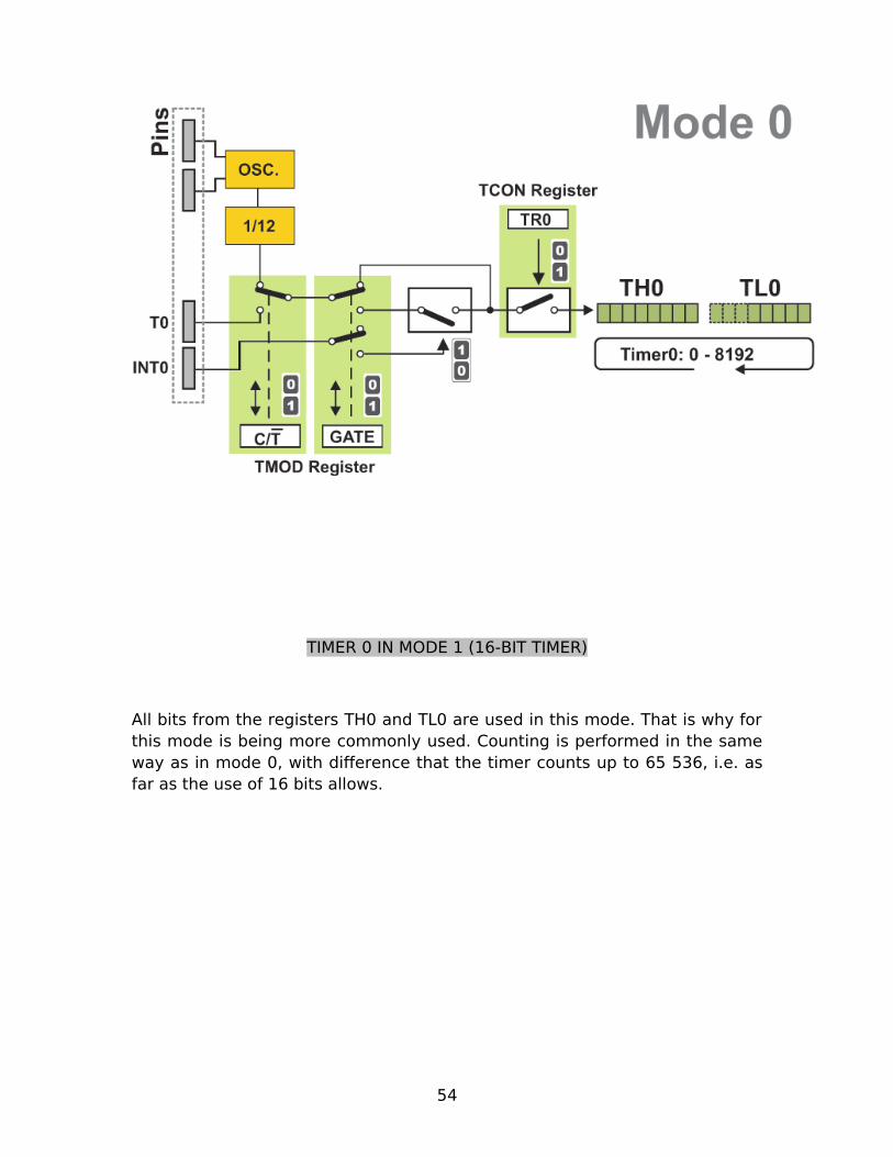
All bits from the registers TH0 and TL0 are used in this mode. That is why for this mode is being more commonly used. Counting is performed in the same way as in mode 0, with difference that the timer counts up to 65 536, i.e. as far as the use of 16 bits allows.
54

TIMER 0 IN MODE 2 (AUTO-RELOAD TIMER)
What does auto-reload mean? Simply, it means that such timer uses only one 8-bit register for counting, but it never counts from 0 but from an arbitrary chosen value (0- 255) saved in another register.
The advantages of this way of counting are described in the following example: suppose that for any reason it is continuously needed to count up 55 pulses at a time from the clock generator.
When using mode 1 or mode 0, it is needed to write number 200 to the timer registers and check constantly afterwards whether overflow occurred, i.e. whether the value 255 is reached by counting. When it has occurred, it is needed to rewrite number 200 and repeat the whole procedure. The microcontroller performs the same procedure in mode 2 automatically. Namely, in this mode it is only register TL0 operating as a timer (normally 8-bit), while the value from which counting should start is saved in the TH0 register. Referring to the previous example, in order to register each 55th pulse, it is needed to write the number 200 to the register and configure the timer to operate in mode 2.
55

TIMER 0 IN MODE 3 (SPLIT TIMER)
By configuring Timer 0 to operate in Mode 3, the 16-bit counter consisting of two registers TH0 and TL0 is split into two independent 8-bit timers. In addition, all control bits which belonged to the initial Timer 1 (consisting of the registers TH1 and TL1), now control newly created Timer 1. This means that even though the initial Timer 1 still can be configured to operate in any mode ( mode 1, 2 or 3 ), it is no longer able to stop, simply because there is no bit to do that. Therefore, in this mode, it will uninterruptedly “operate in the background “.
56
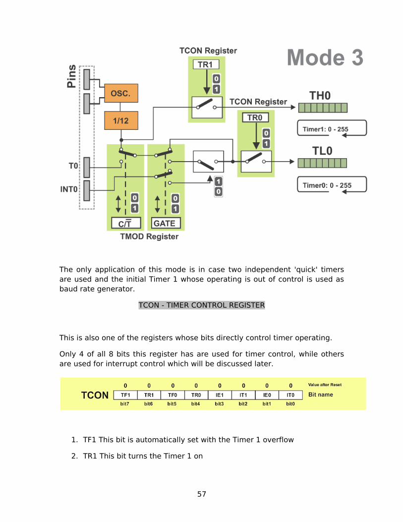
The only application of this mode is in case two independent 'quick' timers are used and the initial Timer 1 whose operating is out of control is used as baud rate generator.
TCON - TIMER CONTROL REGISTER
This is also one of the registers whose bits directly control timer operating.
Only 4 of all 8 bits this register has are used for timer control, while others are used for interrupt control which will be discussed later.
1. TF1 This bit is automatically set with the Timer 1 overflow
2. TR1 This bit turns the Timer 1 on
57

a. 1 - Timer 1 is turned on
b. 0 - Timer 1 is turned off
3. TF0 this bit is automatically set with the Timer 0 overflow.
4. TR0 This bit turns the timer 0 on
a. 1 - Timer 0 is turned on
b. 0 - Timer 0 is turned off
HOW TO START TIMER 0?
Normally, first this timer and afterwards its mode should be selected. Bits which control that are resided in the register TMOD:
This means that timer 0 operates in mode 1 and counts pulses from internal source whose frequency is equal to 1/12 the quartz frequency.
In order to enable the timer, turn it on:
58

Immediately upon the bit TR0 is set, the timer starts operating. Assuming that a quartz crystal with frequency of 12MHz is embedded, a number it contains will be incremented every microsecond. By counting up to 65.536 microseconds, the both registers that timer consists of will be set. The microcontroller automatically reset them and the timer keeps on repeating counting from the beginning as far as the bit’s value is logic one (1).
HOW TO 'READ' A TIMER?
Depending on the timer’s application, it is needed to read a number in the timer registers or to register a moment they have been reset.
- Everything is extremely simple when it is needed to read a value of the timer which uses only one register for counting (mode 2 or Mode 3). It is sufficient to read its state at any moment and it is it!
- It is a bit complicated to read a timer’s value when it operates in mode 2. Assuming that the state of the lower byte is read first (TL0) and the state of the higher byte (TH0) afterwards, the result is:
TH0 = 15 TL0 = 255
Everything seems to be in order at first sight, but the current state of register at the moment of reading was:
TH0 = 14 TL0 = 255
59

In case of negligence, this error in counting (255 pulses) may occur for not so obvious but quite logical reason. Reading the lower byte is correct ( 255 ), but at the same time the program counter “ was taking “ a new instruction for the TH0 state reading, an overflow occurred and both registers have changed their contents ( TH0: 14→15, TL0: 255→0). The problem has simple solution: the state of the higher byte should be read first, then the state of the lower byte and once again the state of the higher byte. If the number stored in the higher byte is not the same both times it has been read then this sequence should be repeated ( this is a mini- loop consisting of only 3 instructions in a program).
There is another solution too. It is sufficient to simply turn timer off while reading (the bit TR0 in the register TCON should be 0), and turn it on after that
UART (UNIVERSAL ASYNCHRONOUS RECEIVER AND TRANSMITTER)
One of the features that make this microcontroller so powerful is an integrated UART, better known as a serial port. It is a duplex port, which means that it can transmit and receive data simultaneously. Without it, serial data sending and receiving would be endlessly complicated part of the program where the pin state continuously is being changed and checked according to strictly determined rhythm. Naturally, it does not happen here because the UART resolves it in a very elegant manner. All the programmer needs to do is to simply select serial port mode and baud rate. When the programmer is such configured, serial data sending is done by writing to the register SBUF while data receiving is done by reading the same register. The microcontroller takes care of all issues necessary for not making any error during data exchange.
Serial port should be configured prior to being used. That determines how many bits one serial “word” contains, what the baud rate is and what the pulse source for synchronization is. All bits controlling this are stored in the SFR Register SCON (Serial Control).
SCON REGISTER (SERIAL PORT CONTROL REGISTER)
60

1. SM0 - bit selects mode
2. SM1 - bit selects mode
3. SM2 - bit is used in case that several microcontrollers share the same interface. In normal circumstances this bit must be cleared in order to enable connection to function normally.
4. REN - bit enables data receiving via serial communication and must be set in order to enable it.
5. TB8 - Since all registers in microcontroller are 8-bit registers, this bit solves the problem of sending the 9th bit in modes 2 and 3. Simply, bits content is sent as the 9th bit.
6. RB8 - bit has the same purpose as the bit TB8 but this time on the receiver side. This means that on receiving data in 9-bit format, the value of the last (ninth) appears on its location.
7. TI - bit is automatically set at the moment the last bit of one byte is sent when the USART operates as a transmitter. In that way processor “knows” that the line is available for sending a new byte. Bit must be clear from within the program!
8. RI - bit is automatically set once one byte has been received. Everything functions in the similar way as in the previous case but on the receive side. This is line a “doorbell” which announces that a byte has been received via serial communication. It should be read quickly prior to a new data takes its place. This bit must also be also cleared from within the program!
As seen, serial port mode is selected by combining the bits SM0 and SM2:
SM0 SM1 Mode Description Baud Rate
0 0 0 8-bit Shift Register 1/12 the quartz frequency
0 1 1 8-bit UARTDetermined by the timer
1
1 0 2 9-bit UART1/32 the quartz frequency
(1/64 the quartz frequency)
61
1 1 3 9-bit UARTDetermined by the timer
1
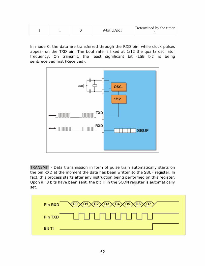
In mode 0, the data are transferred through the RXD pin, while clock pulses appear on the TXD pin. The bout rate is fixed at 1/12 the quartz oscillator frequency. On transmit, the least significant bit (LSB bit) is being sent/received first (Received).
TRANSMIT - Data transmission in form of pulse train automatically starts on the pin RXD at the moment the data has been written to the SBUF register. In fact, this process starts after any instruction being performed on this register. Upon all 8 bits have been sent, the bit TI in the SCON register is automatically set.
62

RECEIVE - Starts data receiving through the pin RXD once two necessary conditions are met: bit REN=1 and RI=0 (both bits reside in the SCON register). Upon 8 bits have been received, the bit RI (register SCON) is automatically set, which indicates that one byte is received.
Since, there are no START and STOP bits or any other bit except data from the SBUF register, this mode is mainly used on shorter distance where the noise level is minimal and where operating rate is important. A typical example for this is I/O port extension by adding cheap IC circuit (shift registers 74HC595, 74HC597 and similar).
MODE 1
In Mode1 10 bits are transmitted through TXD or received through RXD in the following manner: a START bit (always 0), 8 data bits (LSB first) and a STOP bit (always 1) last. The START bit is not registered in this pulse train. Its purpose is to start data receiving mechanism. On receive the STOP bit is automatically written to the RB8 bit in the SCON register.
63

TRANSMIT - A sequence for data transmission via serial communication is automatically started upon the data has been written to the SBUF register. End of 1 byte transmission is indicated by setting the TI bit in the SCON register.
RECEIVE - Receiving starts as soon as the START bit (logic zero (0)) appears on the pin RXD. The condition is that bit REN=1and bit RI=0. Both of them are stored in the SCON register. The RI bit is automatically set upon receiving has been completed.
64

The Baud rate in this mode is determined by the timer 1 overflow time.
MODE 2
In mode 2, 11 bits are sent through TXD or received through RXD: a START bit (always 0), 8 data bits (LSB first), additional 9th data bit and a STOP bit (always 1) last. On transmit; the 9th data bit is actually the TB8 bit from the SCON register. This bit commonly has the purpose of parity bit. Upon transmission, the 9th data bit is copied to the RB8 bit in the same register (SCON).The baud rate is either 1/32 or 1/64 the quartz oscillator frequency.
TRANSMIT - A sequence for data transmission via serial communication is automatically started upon the data has been written to the SBUF register. End of 1 byte transmission is indicated by setting the TI bit in the SCON register.
65

RECEIVE - Receiving starts as soon as the START bit (logic zero (0)) appears on the pin RXD. The condition is that bit REN=1and bit RI=0. Both of them are stored in the SCON register. The RI bit is automatically set upon receiving has been completed.
MODE 3
Mode 3 is the same as Mode 2 except the baud rate. In Mode 3 is variable and can be selected. Baud Rate is defined as a number of send/received bits per second. In case the UART is used, baud rate depends on: selected mode, oscillator frequency and in some cases on the state of the bit SMOD stored in the SCON register.
C PROGRAMMING FOR 8051 USING KEIL IDE
FROM THE C PROGRAM TO THE MACHINE LANGUAGE
66

The C source code is very high level language, meaning that it is far from being at the base level of the machine language that can be executed by a processor. This machine language is basically just zero’s and one's and is written in Hexadecimal format, that why they are called HEX files. There are several types of HEX files; we are going to produce machine code in the INTEL HEX-80 format, since this is the output of the KEIL IDE that we are going to use. Figure shows that to convert a C program to machine language, it takes several steps depending on the tool you are using, however, the main idea is to produce a HEX file at the end. This HEX file will be then used by the 'burner' to write every byte of data at the appropriate place in the EEPROM of the 89S52.
ORGANIZATION OF A C PROGRAM
All C programs have this common organization scheme, sometimes it's followed, sometimes it's not, however, it is imperative for this category of programming that this organization scheme be followed in order to be able to develop your applications successfully. Any application can be divided into the following parts, noting that is should be written in this order:
A. Headers Includes and constants definitions
67

In this part, header files (.h) are included into your source code. Those headers files can be system headers to declare the name of SFRs, to define new constants, or to include mathematical functions like trigonometric functions, root square calculations or numbers approximations. Header files can also contain your own functions that would be shared by various programs.
B. Variables declarations
More precisely, this part is dedicated to ‘Global Variables’ declarations. Variables declared in this place can be used anywhere in the code. Usually in microcontroller programs, variables are declared as global variables instead of local variables, unless you are running short of RAM memory and want to save some space, so we use local variables, whose values will be lost each time you switch from a function to another. To summarize, global variables as easier to use and implement than local variables, but they consume more memory space.
D. functions' body
Here you group all your functions. Those functions can be simple ones that can be called from another place in your program, as they can be called from an 'interrupt vector'. In other words, the sub-programs to be executed when an interrupt occurs are also written in this place.
E. Initialization
The particularity of this part is that it is executed only one time when the microcontroller was just subjected to a 'RESET' or when power is just switched ON, then the processor continue executing the rest of the program but never executes this part again. This particularity makes it the perfect place in a program to initialize the values of some constants, or to define the mode of operation of the timers, counters, interrupts, and other features of the microcontroller.
F. Infinite loop
An infinite loop in a microcontroller program is what is going to keep it alive, because a processor have to be allays running for the system to function, exactly like a heart have to be always beating for a person to live. Usually this part is the core of any program, and it’s from here that all the other functions are called and executed.
68

PROGRAM FOR MOTOR CONTROLLED LAND ROVER
#include<REG52.H>
sbit DTMF = P1^3;
sbit ENABLE = P0^7;
sbit MOTOR_2 = P0^1;
sbit MOTOR_1 = P0^0;
void main()
{
char Temp_Buffer;
P1 = 0XFF;
DTMF = 1;
ENABLE = 0;
MOTOR_2 = 0;
MOTOR_1 = 0;
while (1)
{
P1 = 0XFF;
while(DTMF == 0);
Temp_Buffer = (P1 & 0XF0);
switch(Temp_Buffer)
{
case 0x80: {
}
69

case 0x40: {
}
case 0xC0: {
}
case 0x20: {
}
case 0x60: {
}
case 0x10: {
ENABLE = 1;
MOTOR_2 = 1;
MOTOR_1 = 1;
break;
}
case 0xE0: {
ENABLE = 1;
MOTOR_2 = 1;
MOTOR_1 = 0;
break;
}
case 0x90: {
ENABLE = 1;
MOTOR_2 = 0;
MOTOR_1 = 1;
break;
}
70

case 0x50: {
ENABLE = 1;
MOTOR_2 = 0;
MOTOR_1 = 0;
break;
}
case 0xA0: {
ENABLE = 0;
MOTOR_2 = 0;
MOTOR_1 = 0;
break;
}
default: break;
}
}
}
6 PIN DIP PHOTOTRANSISTOR PHOTOCOUPLER MCT2E
71
FEATURES
1. TIL11X series: TIL111, TIL117
2. MCT2X series: MCT2, MCT2E
3. High isolation voltage between input and output Viso = 5000 Vrms
4. Cree page distance >7.6mm
5. Compact dual-in-line package
6. Operating temperature up to +110°C
7. Pb free and RoHS compliant.
8. UL approved (No. E214129)
9. VDE approved (No. 132249)
10.SEMKO approval (No.716108 / No. 716109)
11.NEMKO approved (No. P06206474)
12.DEMKO approved (No. 313924)
13.FIMKO approved (No. FI 22807)
14.CSA approval (No.1969132)
DESCRIPTION
The TIL11X series and MCT2X series of devices each consist of an infrared emitting diode optically coupled to a phototransistor detector. They are packaged in a 6-pin DIP package and available in wide-lead spacing and SMD option.
An opto-isolator (or optical isolator, optocoupler, photocoupler, or photoMOS)
is a device that uses a short optical transmission path to transfer a signal
between elements of a circuit, typically a transmitter and a receiver, while
keeping them electrically isolated — since the signal goes from an electrical
signal to an optical signal back to an electrical signal, electrical contact along
the path is broken.
APPLICATIONS
1. Power supply regulators
72

2. Digital logic inputs
3. Microprocessor inputs
4. Appliance system
5. Industrial controls
PIN DESCRIPTION
73

1. Anode
2. Cathode
3. No Connection
4. Emitter
5. Collector
6. Base
MOTOR DRIVER
L293D QUADRUPLE HALF-H DRIVERS
1. Featuring Unitrode L293 and L293D
2. Products Now From Texas Instruments
3. Wide Supply-Voltage Range: 4.5 V to 36 V
4. Separate Input-Logic Supply
5. Internal ESD Protection
6. Thermal Shutdown
7. High-Noise-Immunity Inputs
8. Functionally Similar to SGS L293 and SGS L293D
9. Output Current 1 A Per Channel (600 mA for L293D)
10.Peak Output Current 2 A Per Channel (1.2 A for L293D)
11.Output Clamp Diodes for Inductive
12.Transient Suppression (L293D)
DESCRIPTION
The L293 and L293D are quadruple high-current half-H drivers. The L293 is designed to provide bidirectional drive currents of up to 1 A at voltages from 4.5 V to 36 V. The L293D is designed to provide bidirectional drive currents of up to 600-mA at voltages from 4.5 V to 36 V. Both devices are designed to drive inductive loads such as relays, solenoids, dc and bipolar stepping
74

motors, as well as other high-current/high-voltage loads in positive-supply applications.
All inputs are TTL compatible. Each output is a complete totem-pole drive circuit, with a Darlington transistor sink and a pseudo-Darlington source. Drivers are enabled in pairs, with drivers 1 and 2 enabled by 1,2EN and drivers 3 and 4 enabled by 3,4EN. When an enable input is high, the associated drivers are enabled, and their outputs are active and in phase with their inputs. When the enable input is low, those drivers are disabled, and their outputs are off and in the high-impedance state. With the proper data inputs, each pair of drivers forms a full-H (or bridge)reversible drive suitable for solenoid or motor applications.
BLOCK DIAGRAM
75

LOGIC DIAGRAM
76

77

MC78XX/LM78XX/MC78XXA
3-Terminal 1A Positive Voltage Regulator
DESCRIPTION
The MC78XX/LM78XX/MC78XXA series of three terminal positive regulators are available in the TO-220/D-PAK package and with several fixed output voltages, making them useful in a wide range of applications. Each type employs internal current limiting, thermal shut down and safe operating area protection, making it essentially indestructible. If adequate heat sinking is provided, they can deliver over 1A output current. Although designed primarily as fixed voltage regulators, these devices can be used with external components to obtain adjustable voltages and currents. This voltage regulators offers impressive performance advantages over old-fashioned zener diode-resistor combinations, providing lower output impedance and reduced quiescent current.
FEATURES
1. Output Current up to 1A
2. Output Transistor Safe Operating Area Protection
3. Output Voltages 5V, 6V, 8V, 9V, 10V, 12V, 15V, 18V and24V
4. 3- Terminal Regulators
5. No External Components Required
6. Internal Thermal Overload Protection
7. Internal Short Circuit Current-Limiting
8. Available in TO-92, SOT-89 and SOP-8 packages
9. Suitable for C-MOS, TTL, the other Digital IC’s power supply
78

EQUIVALENT CIRCUIT
79
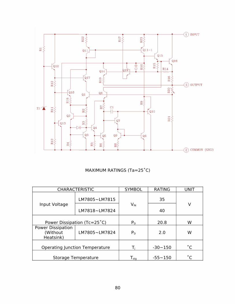
MAXIMUM RATINGS (Ta=25˚C)
CHARACTERISTIC SYMBOL RATING UNIT
Input VoltageLM7805~LM7815
VIN
35V
LM7818~LM7824 40
Power Dissipation (Tc=25˚C) PD 20.8 WPower Dissipation
(Without Heatsink)
LM7805~LM7824 PD 2.0 W
Operating Junction Temperature Tj -30~150 ˚C
Storage Temperature Tstg -55~150 ˚C
80

81

82

83

TO – 220
84

D – PAK
85

REGULATED POWER SUPPLY
INTRODUCTION – In general electronic circuits like amplifiers, oscillators require a source of DC power. Batteries, no doubt may be used for power supply in portable electronic equipment. But, batteries are rarely used for this purpose as they are costly and require frequency replacement. In practice, DC power for electronic circuits is most conveniently obtained from commercial AC lines by using rectifier-filter-regulator, called a power supply.
DESCRIPTION – A DC power supply, which converts AC into DC and maintains the output voltage constants irrespective of AC mains fluctuations or load variations, is known as regulated DC power supply
The block diagram of regulated power supply is shown below. A power supply consists of rectifier, filter and regulator. The conversion of alternating voltage in to steady voltage by means of rectifier, In order to remove the alternating component of the rectified output (ripples), we need a filter. To obtain constant output voltage irrespective of load variations or supply variations we need a regulator.
BLOCK DIAGRAM
86
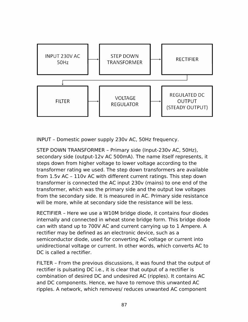
INPUT – Domestic power supply 230v AC, 50Hz frequency.
STEP DOWN TRANSFORMER – Primary side (Input-230v AC, 50Hz), secondary side (output-12v AC 500mA). The name itself represents, it steps down from higher voltage to lower voltage according to the transformer rating we used. The step down transformers are available from 1.5v AC – 110v AC with different current ratings. This step down transformer is connected the AC input 230v (mains) to one end of the transformer, which was the primary side and the output low voltages from the secondary side. It is measured in AC. Primary side resistance will be more, while at secondary side the resistance will be less.
RECTIFIER – Here we use a W10M bridge diode, it contains four diodes internally and connected in wheat stone bridge form. This bridge diode can with stand up to 700V AC and current carrying up to 1 Ampere. A rectifier may be defined as an electronic device, such as a semiconductor diode, used for converting AC voltage or current into unidirectional voltage or current. In other words, which converts AC to DC is called a rectifier.
FILTER – From the previous discussions, it was found that the output of rectifier is pulsating DC i.e., it is clear that output of a rectifier is combination of desired DC and undesired AC (ripples). It contains AC and DC components. Hence, we have to remove this unwanted AC ripples. A network, which removes/ reduces unwanted AC component
87

from the output of a rectifier is called filter. We use 1000uF/25V electrolytic capacitor. It is a polar capacitor.
VOLTAGE REGULATOR OR STABILIZATION – It is observed that output voltage of a power supply decreases with increase in the current drawn by the load. As the current increases, the drop across the diodes, transformer windings. Thus, the voltage available at the output decreases. Also, there is a possibility of voltage fluctuations in the mains power supply due to distribution/ transmission. But, the electronic devices/ circuits are very sensitive to DC voltage increase, the device/ circuit/ equipment may get damaged. When the DC voltage decreases below the stipulated value, the equipment/ circuit may not perform properly. Hence, the fluctuations in the DC voltages had to be regulated. In order to ensure this, a voltage stabilizer (IC REGULATOR) circuit is used.
REGULATED POWER SUPPLY
There are many types of power supply. Most are designed to convert high voltage AC mains electricity to a suitable low voltage supply for electronics circuits and other devices. A power supply can by broken down into a series of blocks, each of which performs a particular function.
For example a 5V regulated supply:
88
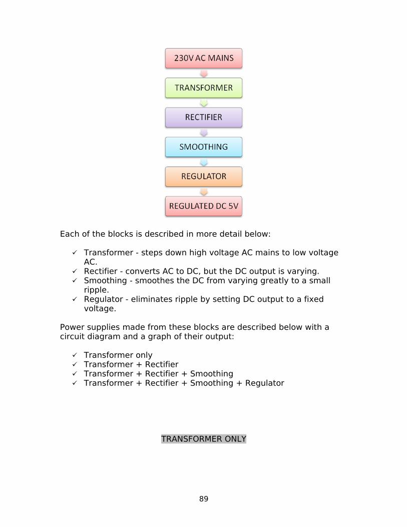
Each of the blocks is described in more detail below:
Transformer - steps down high voltage AC mains to low voltage AC.
Rectifier - converts AC to DC, but the DC output is varying. Smoothing - smoothes the DC from varying greatly to a small
ripple. Regulator - eliminates ripple by setting DC output to a fixed
voltage.
Power supplies made from these blocks are described below with a circuit diagram and a graph of their output:
Transformer only Transformer + Rectifier Transformer + Rectifier + Smoothing Transformer + Rectifier + Smoothing + Regulator
TRANSFORMER ONLY
89

The low voltage AC output is suitable for lamps, heaters and special AC motors. It is not suitable for electronic circuits unless they include a rectifier and a smoothing capacitor.
TRANSFORMER + RECTIFIER
The varying DC output is suitable for lamps, heaters and standard motors. It is not suitable for electronic circuits unless they include a smoothing capacitor.
TRANSFORMER + RECTIFIER + SMOOTHING
The smooth DC output has a small ripple. It is suitable for most electronic circuits.
90

Transformer + Rectifier + Smoothing + REGULATOR
The regulated DC output is very smooth with no ripple. It is suitable for all electronic circuits.
91

TRANSFORMER
Transformers convert AC electricity from one voltage to another with little loss of power. Transformers work only with AC and this is one of the reasons why mains electricity is AC.
Step-up transformers increase voltage, step-down transformers reduce voltage. Most power supplies use a step-down transformer to reduce the dangerously high mains voltage (230V in UK) to a safer low voltage.
The input coil is called the primary and the output coil is called the secondary. There is no electrical connection between the two coils; instead they are linked by an alternating magnetic field created in the soft-iron core of the transformer. The two lines in the middle of the circuit symbol represent the core.
Transformers waste very little power so the power out is (almost) equal to the power in. Note that as voltage is stepped down current is stepped up.
The ratio of the number of turns on each coil, called the turn’s ratio, determines the ratio of the voltages. A step-down transformer has a large number of turns on its primary (input) coil which is connected to the high voltage mains supply, and a small number of turns on its secondary (output) coil to give a low output voltage.
TURNS RATIO = Vp
= Np
AND POWER OUT = POWER IN
Vs Ns Vs × Is = Vp × Ip
Vp = primary (input) voltageNp = number of turns on primary coilIp = primary (input) current
Vs = secondary (output) voltageNs = number of turns on secondary coilIs = secondary (output) current
92

RECTIFIER
There are several ways of connecting diodes to make a rectifier to convert AC to DC. The bridge rectifier is the most important and it produces full-wave varying DC. A full-wave rectifier can also be made from just two diodes if a centre-tap transformer is used, but this method is rarely used now that diodes are cheaper. A single diode can be used as a rectifier but it only uses the positive (+) parts of the AC wave to produce half-wave varying DC.
BRIDGE RECTIFIER
A bridge rectifier can be made using four individual diodes, but it is also available in special packages containing the four diodes required. It is called a full-wave rectifier because it uses all the AC wave (both positive and negative sections). 1.4V is used up in the bridge rectifier because each diode uses 0.7V when conducting and there are always two diodes conducting, as shown in the diagram below. Bridge rectifiers are rated by the maximum current they can pass and the maximum reverse voltage they can withstand (this must be at least three times the supply RMS voltage so the rectifier can withstand the peak voltages). Please see the Diodes page for more details, including pictures of bridge rectifiers.
93
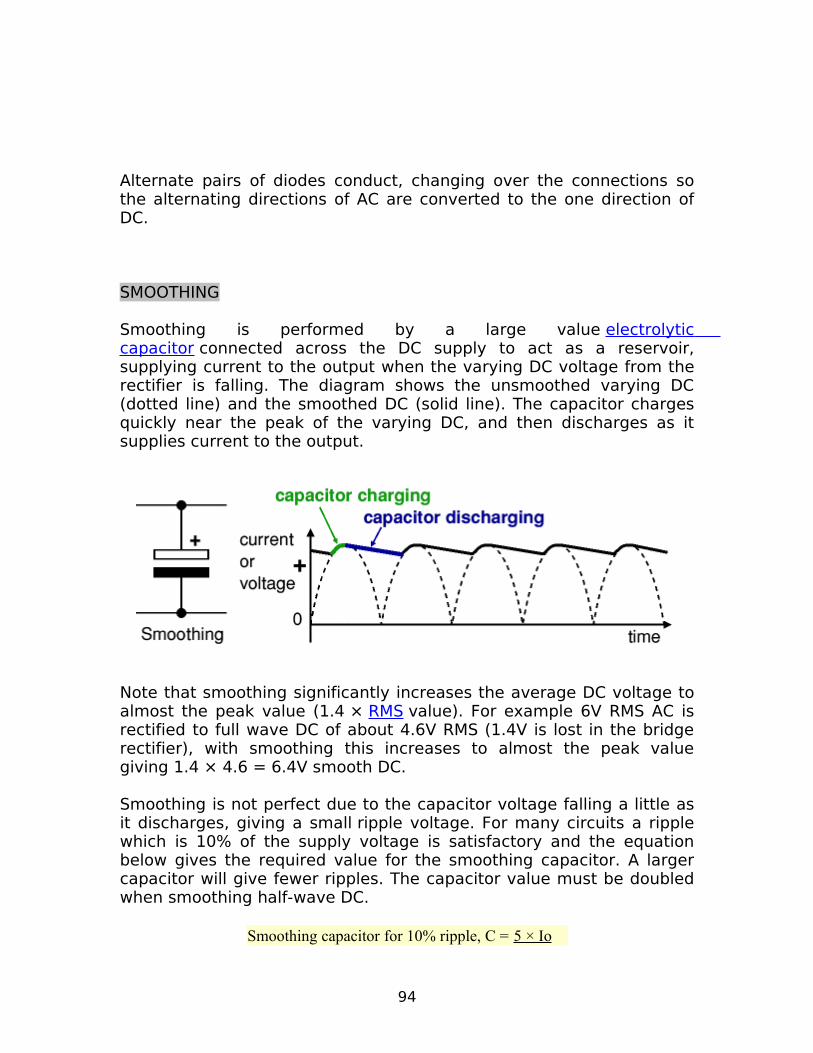
Alternate pairs of diodes conduct, changing over the connections so the alternating directions of AC are converted to the one direction of DC.
SMOOTHING
Smoothing is performed by a large value electrolytic capacitor connected across the DC supply to act as a reservoir, supplying current to the output when the varying DC voltage from the rectifier is falling. The diagram shows the unsmoothed varying DC (dotted line) and the smoothed DC (solid line). The capacitor charges quickly near the peak of the varying DC, and then discharges as it supplies current to the output.
Note that smoothing significantly increases the average DC voltage to almost the peak value (1.4 × RMS value). For example 6V RMS AC is rectified to full wave DC of about 4.6V RMS (1.4V is lost in the bridge rectifier), with smoothing this increases to almost the peak value giving 1.4 × 4.6 = 6.4V smooth DC.
Smoothing is not perfect due to the capacitor voltage falling a little as it discharges, giving a small ripple voltage. For many circuits a ripple which is 10% of the supply voltage is satisfactory and the equation below gives the required value for the smoothing capacitor. A larger capacitor will give fewer ripples. The capacitor value must be doubled when smoothing half-wave DC.
Smoothing capacitor for 10% ripple, C = 5 × Io
94

Vs × f
C = smoothing capacitance in farads (F)Io = output current from the supply in amps (A)
Vs = supply voltage in volts (V), this is the peak value of the unsmoothed DCf = frequency of the AC supply in hertz (Hz), 50Hz in the UK
REGULATOR
Voltage regulator ICs are available with fixed (typically 5, 12 and 15V) or variable output voltages. They are also rated by the maximum current they can pass. Negative voltage regulators are available, mainly for use in dual supplies. Most regulators include some automatic protection from excessive current ('overload protection') and overheating ('thermal protection').
Many of the fixed voltage regulator ICs has 3 leads and look like power transistors, such as the 7805 +5V 1A regulator shown on the below. They include a hole for attaching a heat sink if necessary.
SINGLE-PHASE GLASS PASSIVATED
SILICON BRIDGE RECTIFIER
VOLTAGE RANGE 50 to 1000 Volts CURRENT 1.5 Amperes
FEATURES
1. High reverse voltage to 1000V
2. Surge overload ratings to 50 amperes peak
3. Good for printed circuit board assembly
4. Mounting position: Any
5. Weight: 1.20 grams
6. Diffused Junction
7. Low Forward Voltage Drop
8. High Current Capability
95

9. High Reliability
INTRODUCTION TO BASIC ELECTRONICS
COMPONENTS SYMBOLS
ELECTRONIC COMPONENTS ARE CLASSED INTO EITHER BENG PASSIVE DEVICES OR ACTIVE DEVICES
A PASSIVE DEVICES is one that contributes no power gain (amplification) to a circuit or system. It has no control action and does not require any input other than a signal to perform its function. In other words, “components with no brains!” examples are resistors, capacitors and inductors
ACTIVE DEVICES are components that are capable of controlling voltages are current and can create a switching action in the circuit. In other words, “devices with smarts!” examples are diodes, transistors and integrated circuits. Most active components are semiconductors.
RESISTORS – This is the most common component in electronics. It is used mainly to control current and voltage within the circuit. You can identify simple resistor by its simple cigar shape with a wire lead coming out of each end. It uses a system of color coded bands to identify the value of the component (measured in ohms). A surface mount resistor is in fact mere millimeter in size but performs the same function as its bigger brother, the simple resistor a potentiometer is a variable resistor. It lets you vary the resistance with a dial or sliding control in order to alter current or voltage on the fly. This is opposed to the fixed simple resistors.
96

MNEMONIC PHRASES FOR REMEMBERING CODES
There are many mnemonic phrases used to remember the order of the colors.
The easiest way to remember the colors is probably to think of the color spectrum, then add in the numbers. Starting at the lowest values, one goes from black (no color) to brownish (infrared) red (2) green (5) to blue (6) and from there to ultraviolet, almost white, and white light.
Bye Bye Rose, Off You Go - Birmingham Via Great Western Bad Boys Ring Our Young Girls But Violet Giggles Willingly Bad Bacon Rots Our Young Guts But Venison Goes Well. Get Some Now! B.B. ROY of Great Britain had a Very Good Wife, Good Son Buffalo Bill Roamed Over Yellow Grass Because Vistas Grand Were God's Sanctuary Bully Brown Ran Over a Yodeling Goat, Because Violet's Granny Was Gone Snorkeling Buy Better Resistance Or Your Grid Bias May Go Wrong Bad Beer Rots Our Young Guts But Vodka Goes Well Good Sir. Bongo's Buy Randy Ocelot Young Girls Buy Very Groovy Walruses Black Beetles Running Over Your Garden Bring Very Good Weather Black Brown Richard Of York Gave Battle In Vain and the Good Women Grieve Sadly
All of the above are mnemonics for the order: Black Brown Red Orange Yellow Green Blue Violet Gray White (Gold Silver None)
THE COLOUR CODE TABLE
Colour Digit Multiplier Tolerance
Black 0 1
Brown 1 10 ± 1%
Red 2 100 ± 2%
Orange 3 1K
Yellow 4 10K
Green 5 100K ± 0.5%
97

Blue 6 1M ± 0.25%
Violet 7 10M ± 0.1%
Grey 8
White 9
Gold 0.1 ± 5%
Silver 0.01 ± 10%
None ± 20%
COLOUR CODES VALUES
The resistance value, tolerance, and watt rating of the resistor are generally printed onto the body of the resistor when it is big enough to read the print, such as large power resistors. When resistors are small such as 1/4W carbon and film types, these specifications must be shown in some other manner as the print would be too small to read. So to over come this, small resistors use coloured paint bands to indicate the resistance value and tolerance with the physical size of the resistor indicating its wattage rating.
An International resistor colour coding scheme was developed many years ago as a simple way of identifying resistor values. It consists of coloured rings (in spectral order) whose meaning is illustrated below
98
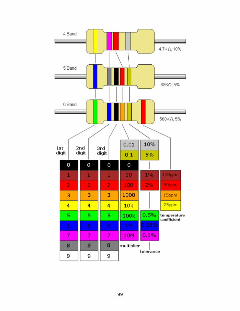
99
CONDENSORS/CAPACITORS – Capacitors, or caps, vary in size and shape from a small surface mount model up to a huge electric motor cap the size of paint can. It stores electrical energy in the form of electrostatic charge. The size of a capacitor generally determines how much charge it can store. A small surface mount or ceramic cap will only hold a minuscule charge. A cylindrical electrolytic cap will store a much larger charge. Some of the large electrolytic caps can store enough charge to kill a person. Another type, called tantalum capacitors, stores a large charge in a smaller package.
INDUCTORS – You may remember from science class that adding electrical current to a coil of wire produces a magnetic field around itself. This is how the inductor works. It is charged with a magnetic field and when that field collapses it produces current in the opposite direction. Inductors are used in alternating current circuits to oppose changes in the existing current. Most inductors can be identified by the coil appearance. Others actually look like a resistor but are usually green in color.
DIODES – Diodes are basically a one-way valve for electrical current. They let it flow in one direction (from positive to negative) and not in the other direction. This is used to perform rectification or conversion of ac current to dc by clipping off the negative portion of an ac waveform. The diode terminals are cathode and anode and the arrow inside the diode symbol points towards the cathode, indicating current flow in that direction when the diode is forward biased and conducting current. Most diodes are similar in appearance to a resistor and will have a painted line on one end showing the direction or flow (white side is negative). If the negative side is on the negative end of the circuit, current will flow. If negative is on the positive side of the circuit no current will flow.
LEDs (LIGHT EMITTING DIODES) – LEDs are simply diodes that emit light of one form or another. They are used as indicator devices. Example: LED lit equals machine on. The general purpose silicon diode emits excess energy in the form of heat when conducting current. If a different semiconductor material such as gallium, arsenide phosphate is used, the excess energy can be released at a lower wavelength visible to human eye. This is the composition of LED. They come in several sizes and colors. Some even emit infrared light which cannot be seen by the human eye.
SWITCH – This is a mechanical part which when pressed makes the current to flow through it, if the switch is released the current stops flowing through it. This helps to control a circuit.
TRANSISTORS – The transistor performs two basic functions.
1. It acts as a switch turning current on and off.
100

2. It acts as an amplifier. This makes an output signal that is a magnified version of the input signal.
Transistors come in several sizes depending on their application. It can be a big power transistor such as is used in power amplifiers in your stereo, down to a surface mount (SMT) and even down to .5 microns wide such as in a microprocessor or integrated circuit.
NPN TRANSISTORS
Bipolar junction performs the function of amplifications where a small varying voltage or current applied to the base is proportionately replicated by a much larger voltage or current between the collector and emitter leads. Bipolar junction refers to sandwich construction of the semiconductor, where a wedge of “P” material is placed between two wedges of “N” material. In this NPN construction a small base current controls the larger current flowing from collector to emitter.
PNP TRANSISTORS
Similar to NPN transistors, PNP’s have a wedge of “N” material between two wedges of “P” material. In this design, a base current regulates the larger current flowing from emitter to collector, as indicated by the direction of the arrow on the emitter lead.
PCB’s
PCB stands for printed circuit board which is used for wiring up of the components of a circuit. PCB’s are made of paper phenolic FR2 grade (low cost, for low frequency and low power circuit assembly) and glass epoxy FR4 grade (for high frequency, high power circuits) copper clad laminates (available in 1.6mm, 2.4mm and 3.6mm thickness). Single-sided PCB’s have copper foil only on one side while double-sided PCB’s have copper foil on both side of the laminate. Thickness of copper foil is 35 micrometer minimum on cheaper PCB’s and 70 micrometer on slightly costlier PCB’s. Tracks (conductive paths) are made by masking (covering) the track part of copper with etch-resist enamel paint (you can even use nail polish) and later dipping the laminate in ferric chloride solutions to dissolve all copper except under the masked part. Holes in PCB’s are drilled after etching is over. The tracks on two sides of a PCB are joined using printed through hole (PTH) technique, which is equivalent to using slotted copper Rivets for joining tracks on both sides. On cheaper PCB’s, PTH are not provided, only pads (i.e. circular copper land with centre hole) are provided and you have to join the tracks on both
101

sides by soldering a copper wire to the pads with a copper wire. In single-sided PCB components are mounted on the side which has no track (called component side). In a double-sided PCB the component side is defined (masked before hand) or it will show component outline (also called silk screen).
Green masking is the process of applying a layer of green color insulation varnish on all parts of tracks except near the holes, to protect the tracks from exposure to atmosphere and thus prolong its life and reliability.
ICs (INTEGRATED CIRCUITS)
Integrated Circuits or IC’s are complex circuits inside one simple package. Silicon and metals are used to simulate resistors, capacitors, transistors, etc. It is a space saving miracle. These components cone in a wide variety of packages and sizes. You can tell them by their “monolithic shape” that has a ton of “pins” coming out of them. Their applications are as varied as their packages. It can be a simple timer, to a complex logic circuit, or even a microcontroller (microprocessor with a few added functions) with erasable memory built inside.
Document BySANTOSH BHARADWAJ REDDYEmail: [email protected]
Engineeringpapers.blogspot.comMore Papers and Presentations available on above site
102