more and juno ka-band transponder design, performance
TRANSCRIPT
MORE AND JUNO KA-BAND TRANSPONDER DESIGN, PERFORMANCE, QUALIFICATION AND IN-FLIGHT VALIDATION
S. Ciarcia1, L. Simone1, D. Gelfusa1, P. Colucci1,
G. De Angelis1, F. Argentieri1, L. Iess2, R. Formaro3
1 Thales Alenia Space –Italia, 2 University of Rome – La Sapienza, 3 Italian Space Agency
I. ABSTRACT
This paper presents the Ka-Band Translator/Transponder (KaT) that Thales Alenia Space – Italia has designed, developed and qualified for Radio-Science experiments in the frame of JUNO and BepiColombo programs.
II. JUNO Ka-BAND TRANSLATOR
JUNO’s investigation focuses on four themes: origin, interior structure, atmospheric composition and
dynamics, polar magnetosphere. Using a spinning solar-powered spacecraft, the Juno equipment will obtain global maps of the gravity, magnetic fields, and atmospheric composition of Jupiter from a unique polar orbit with a close perijove. JUNO carries in fact precise, high-sensitivity radiometers, magnetometers, and it provides accurate gravity radio-science capabilities that are supported by the KaT equipment.
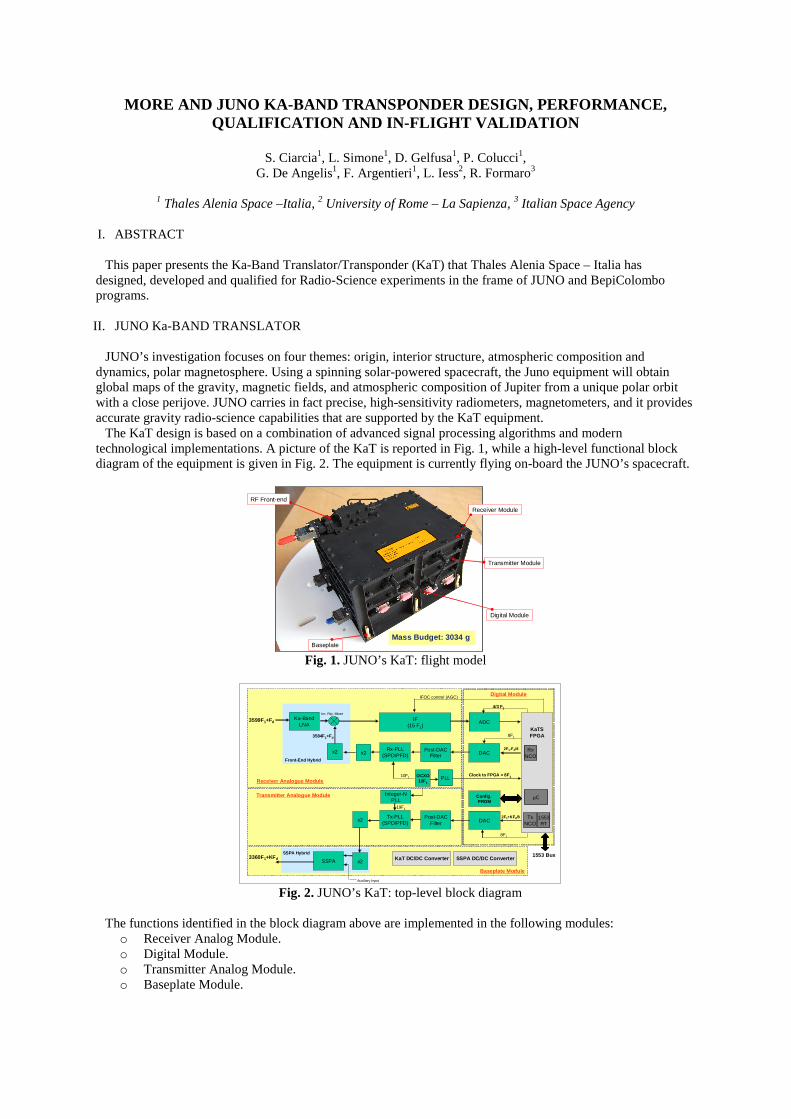
The KaT design is based on a combination of advanced signal processing algorithms and modern technological implementations. A picture of the KaT is reported in Fig. 1, while a high-level functional block diagram of the equipment is given in Fig. 2. The equipment is currently flying on-board the JUNO’s spacecraft.
Mass Budget: 3034 g
RF Front-end
Baseplate
Digital Module
Receiver Module
Transmitter Module
Fig. 1. JUNO’s KaT: flight model
3599F1+Fd IF(15 F1)
ADCKaTSFPGA
DAC
DAC
Rx-PLL(SPD/PFD)
Tx-PLL(SPD/PFD)
3360F1+KFd
4/3 F1
Post-DACFilter
Post-DACFilter
RxNCO
TxNCO
10F1
19F1
x2
SSPA
2F1-Fd/8
2F1+KFd/8
Ka-BandLNA
Im. Rej. Mixer
KaT DC/DC Converter SSPA DC/DC Converter
Receiver Analogue Module
Digital Module
Baseplate Module
Config. PROM
8F1
8F1
Transmitter Analogue Module
x2
OCXO10F1
IFOC control (AGC)
Integer-NPLL µC
1553 Bus
1553RT
PLLClock to FPGA = 8F 1
x2
x2
Front-End Hybrid
SSPA Hybrid
Auxiliary Input
3584F1+Fd
Fig. 2. JUNO’s KaT: top-level block diagram
The functions identified in the block diagram above are implemented in the following modules: o Receiver Analog Module. o Digital Module. o Transmitter Analog Module. o Baseplate Module.

The KaT frequency plan is based on a new Phase-Locked Loop mechanization (so-called Flexible PLL, [4]) that allows achieving the best compromise in terms of phase noise performance, power consumption, hardware complexity and design compactness. A. Receiver Analogue Section
The input signal frequency is equal to 3599F1+Fd, where F1 is defined by the selected communication channel and Fd is the frequency offset due to the Doppler shift and oscillators instabilities (for JUNO mission: F1≅ 9.546146 MHz). After low-noise amplification, the received signal is converted to the IF frequency (i.e. 15F1) using an image rejection mixer whose LO port is controlled by the Rx-PLL (Fig. 4). Note that, as it is shown in Fig. 5 the LNA is implemented as a dedicated hybrid placed on the equipment cover.
WR
28
X 2 Rx-PLL(SPD/PFD)
IF (15*F1)
Ka-Band LNA Image Reject Mixer
3599*F1
3584*F1
X 2Frequency Multiplier
UMS-CHA2066
Triquint TGA4508
Triquint TGA4508
Fig. 3. Receiver front-end schematic
Fig. 4. Receiver front-end hybrid implementation
A wide-band Automatic Gain Control (AGC) is employed in the IF section to keep the signal-plus-noise power constant at the ADC input in order to minimize the noise which arises from the analog-to-digital conversion. The IF section is based on a couple of IFOC (IF-On-Chip) devices. This approach is very attractive in terms of power consumption and design compactness. In fact, the implementation of IF functionalities in CMOS microelectronics yields significant benefits in terms of equipment mass and size reduction. In order to provide radiation hardening in a CMOS integrated-circuit design, the mixed-signal silicon-on-insulator process has been selected by TAS-I for flight applications. In the frame of the SOI approach, the UTSi (Ultra-Thin Silicon) CMOS technology has a completely insulating substrate which provides the required isolation to accommodate RF circuits, analog-to-digital converters and digital logic circuitry, in addition to high quality passive components. The wide-band AGC uses the IFOC built-in digital attenuators which are controlled by the KaT FPGA through a serial interface.
The Rx-PLL (Fig. 5) uses the signal at 10F1 provided by the frequency reference section and the signal at 2F1-Fd/8 from the dedicated DDS. A key element of the loop is the Sampling Phase Detector (SPD), which is a combination of a Step Recovery Diode (SRD) and hot carrier diodes acting as a mixer. A pulse forming circuitry provides a pulse train to the diode gate which generates a comb of harmonics of the input frequency at 10F1. The mixer compares the VCDRO frequency 896F1+Fd/4 with the harmonics, generating a beat note at 4F1-Fd/4. The 4F1-Fd/4 frequency is band-pass filtered and routed to the Phase Frequency Detector (PFD) that compares it with the signal coming from the Rx-DDS. When the carrier recovery loop is locked, the error term maintains the VCDRO at the desired frequency. Finally, the coherent LO frequency (i.e. 3584F1+Fd) is obtained by a x4 frequency multiplication of the VCDRO output.
2F1-Fd/8 InvertingLoopFilter
VCDRO x43584F1+Fd
÷2 BandpassFilter
10F1x90
896F1+Fd/4
4F1-Fd/4
900F
1
2F1-Fd/8
From Rx-DDS
PFD
SPD
Fig. 5. Rx-PLL block diagram
B. Digital Module
The KaT core is implemented in a Digital Module based on the KaT FPGA (RTAX2000S device) performing the following tasks:
o Down-conversion of digital samples to Baseband In-Phase and Quadrature signals.

o Turn-around processing (i.e. coherence). o DDS for both up-link tracking and down-link synthesis.
The KaT FPGA includes a custom Embedded Microcontroller that is devoted to digital receiver configuration, transponder management and data handling functions.
The chosen hardware/software partitioning allows a great flexibility in terms of functions, algorithms and design parameters. As an example, the tracking loops constants can be easily optimized during the receiver tuning phase to obtain the best performance.
The carrier frequency at the ADC input is fixed at 15F1 while the ADC is clocked at 4/3F1. With this approach, only one ADC is required and the phase and amplitude imbalances are avoided, since the mixing is accomplished in the digital domain; in particular, the separation of the in-phase (I) and quadrature (Q) channels is obtained by multiplying the ADC output by the sequence (+1, 0, -1, 0, …) for the I-channel and by the sequence (0, +1, 0, -1, …) for the Q-channel.
The carrier tracking is implemented using the DDS technique. The Q-channel is used as phase error estimation, since it is proportional to the sine of the carrier phase error. The carrier quadrature samples are accumulated to reduce the sampling rate, thus enabling a low-rate implementation of the loop filter wile the carrier recovery loop is based on a 3rd order PLL that allows optimizing the tracking performance even in presence of large Doppler rates. The loop filter outputs the frequency error estimate by adjusting the nominal frequency of the Rx-DDS to 2F1-Fd/8 (see Fig. 5). The carrier recovery loop is finally closed by injecting the Rx-DDS output frequency in the Rx-PLL that provides the coherent LO needed to track the up-link signal.
DAC
ADC Even/Odd Decim.
+1,-1,+1,-1...
Ic(k)
Qc(k)Z-1
+1,-1,+1,-1...
4F1/3
Σ
Rx-NCO
2F1
Fd/8
KaT FPGA
8F1
DAC Tx-NCO
2F1
8F1
Loop
Filt
er
2F1-Fd/8
2F1+KFd/8
15F1
x3599
x3360
εεεεd
KFd/8
+
+
+
-
Microcontroller 1553 RT
Fig. 6. Carrier recovery loop scheme
C. Transmitter Analogue Module The transmitter analog module uses the same PLL implementation as per the receiving section. In this case the
Tx-DDS output frequency is used to set the down-link frequency to the desired value according to the scheme depicted in Fig. 7. The Tx PLL output is followed by a x4 frequency multiplier implemented as two cascaded x2 frequency multipliers. The final power amplification (i.e. 34.5 dBm) is then performed by the Ka-band SSPA integrated in the Baseplate Module.
2F1+KFd/8 LoopFilter
VCDRO3360F1+KFd
÷2 BandpassFilter
19F1x44
840F1+KFd/4
4F1+KFd/4
836F
1
2F1+KFd/8
From Tx-DDS
PFD
SPD
x4
Fig. 7. Tx-PLL block diagram
D. Baseplate Module The Baseplate (Fig. 8) includes the SSPA and two DC/DC converters, i.e.:
o KaT DC/DC Converter, biasing the Receiver Analog module, the Digital module and the Transmitter module;
o SSPA DC/DC Converter, dedicated to the High-Power section.
SSPA
DC/DC Converters
Fig. 8. Baseplate Module layout
External RF IN
Internal RF IN
RF Out
Fig. 9. SSPA layout

TTC 2013 6th ESA International Workshop on Tracking, Telemetry and Command Systems for Space Applications ESA-ESOC, 10 - 13 September 2013
The output power requirement for the KaT (34.5 dBm at 32 GHz) has been implemented by using the line-up schematically reported in the figure hereafter:
TGA4516
IN aux
IN
TGA4040 OUT
2x
TGA4508
Fig. 10. SSPA line-up with two active devices working in parallel
Splitting of the input signal and re-combination of the amplifiers output is carried out using microstrip
technology. Finally, transition to waveguide, both at the input and output port, is implemented by means of a patch-antenna approach. Note that the SSPA section foresees an auxiliary input that is used for supporting the amplification of the Ka-Band down-link coming from the TT&C equipment (Fig. 10). Housing two DC/DC Converters allows maximizing the power conversion efficiency, thus optimizing the on-board power consumption. The two DC/DC converters are based on a Power PCB and a Control PCB. The Power PCB is a single sided board and it supports all the DC/DC converter power devices, namely: the Rad-Hard MOSFETs, Schottky diodes, semiconductor diodes, as well as filters and magnetics, including all the electrical power interconnections. One of the Power PCB side is metalized and screwed on the structure. This approach allows for a high density and low thermal impedance for the above mentioned power devices toward the dissipating base-plate structure. The Power board also offers mechanical support for the Control PCB, which is directly plugged and screwed on its top by using a dedicated pilor.
III. BEPICOLOMBO Ka-BAND TRANSPONDER The main objectives of BepiColombo Mercury Orbiter Radio-Science Experiment (MORE) are the
measurement of the rotational state on Mercury, the measure of the overall structure of the gravity field and an extensive series of tests on the Einstein’s Theory of General Relativity by measuring the orbit of the Planet around the Sun and the propagation of electromagnetic waves to/from the Earth. The MORE KaT includes the following architectural improvements with respect to the JUNO’s version:
o The Digital Module is conceived around the KaT ASIC (0.18 µ technology) that represents a real System-on-Chip integrating custom digital signal processing as well as the LEON2FT Microprocessor [1];
o An On-Board Calibration Module is included for allowing the estimation on the Transponder’s group delay during the mission.
Moreover, the MORE KaT supports wide-band transparent and regenerative ranging that play a fundamental role in the radio-science experiment. The following figures shows the MORE KaT and its top-level block diagram:
Fig. 11. MORE’s KaT: Qualification Model

TTC 2013 6th ESA International Workshop on Tracking, Telemetry and Command Systems for Space Applications ESA-ESOC, 10 - 13 September 2013
3599F1+FdIF
(15 F1)ADC
KaTASIC
DAC
DAC
Rx-PLL(SPD/PFD)
Tx-PLL(SPD/PFD)
3360F1+KFd
20F1
Post-DACFilter
Post-DACFilter
RxNCO
TxNCO
10F1
19F1
PM
SSPA
2F1+Fd/8
2F1+KFd/8
Ka-BandLNA
Im. Rej. Mixer
KaT DC/DC Converter SSPA DC/DC Converter
Receiver Analogue Module Digital Module
Baseplate Module
Config. PROM
10F1
10F1Transmitter Analogue Module
x2
OCXO10F1
IFOC control (AGC)
Integer-NPLL µP
1553 Bus
1553RT
x4
x2
x2
Front-End Hybrid
SSPA Hybrid
3584F1+Fd
x2
RNG
Integer-NPLL
239F1
BandpassFilter
Control fromKaT ASIC
Att.
On-BoardCalibration
Module
40F1
Fig. 12. MORE’s KaT: top-level block diagram
IV. RADIO-SCIENCE PERFORMANCE The following paragraphs provide an overview of the MORE KaT performance concerning the Radio-Science experiment. A. Wide-Band Ranging
The KaT is the first Transponder for Radio-Science that implements a Pseudo-Noise (PN) Ranging modulation scheme at 24.2 Mcps, a huge improvement with respect the precedent equipment. The regenerative ranging scheme selected for the Bepi-Colombo mission is the T2B one which is based on pseudo-noise sequence that can be easily regenerated on-board. The net result of the regeneration would be an increase in the effective return ranging power. This increase would provide some margin for decreasing ranging signal integration time at the ground station, decreasing the power of the return ranging signal transmitted by the transponder, or improving the end-to-end ranging accuracy.
For regenerative ranging, PN binary sequences will be used because they offer a desirable combination of high ranging resolution, low ranging ambiguity, and no need for receivers to "know" when pseudo-noise sequences started as for the sequential ranging. In a transparent ranging channel (i.e. no signal regeneration is carried out on-board), the up-link noise feeds through onto the down-link robbing power from the fundamental ranging sidebands. When on-board regeneration is performed, the ranging signal is detected by a narrow-band tracking loop. In this case the channel noise bandwidth is of a few Hertz instead of several MHz, as for the transparent channel case. In Fig.13 is showed a typical PN Ranging spectrum envelope where, in the centre, is present the modulated residual carrier at 32,1GHz with a strong Clock Component at 12.1 MHz (i.e. at a half of the Chip Rate).
Residual Carrier
PN rangingclock
component
FCHIP
2
Residual Carrier
PN rangingclock
component
FCHIP
2
Fig. 13. Downlink PN Ranging Spectrum at 24.2 Mcps

TTC 2013 6th ESA International Workshop on Tracking, Telemetry and Command Systems for Space Applications ESA-ESOC, 10 - 13 September 2013
According to the block diagram showed in Fig. 14, the regenerative ranging channel includes the following functions [3]:
o Chip Tracking Loop (CTL) for phase and frequency recovery of the code chip and generation of the synchronization signal for the matched filter;
o In-phase Integrator (matched filter) followed by a 3-bit quantization (soft-quantization); o Six Correlators (one for each code component: C1, C2,…,C6) running in parallel for code position
recovery; o Downlink Code Generator for turn-around function; o Control Logic for correlators and code generator management;
Such regenerative ranging processing allows for an acquisition of the ranging probing sequences within a few seconds thus the Radio-Science experiment can be carried out with a negligible outage during the orbiting pass of the spacecraft.
IN-PHASEINTEGRATOR
MID-PHASEINTEGRATOR
NCOTIMINGLOGIC
SIGN
LOOPFILTER
ΣL
÷N Carrier LoopError
Nominal ChipRate
CODE GENERATOR #1
CODE CORRELATOR #1
Code ComponentsGenerators Clock
><
Lock
Dismiss
Majority Voting Logic(JPL ’99, V2, V4)
Lock Status
C1
CODE GENERATOR #2
CODE CORRELATOR #2 ><
Dismiss
C2
CODE GENERATOR #3
CODE CORRELATOR #3 ><
Dismiss
C3
CODE GENERATOR #4
CODE CORRELATOR #4 ><
Dismiss
C4
CODE GENERATOR #5
CODE CORRELATOR #5 ><
Dismiss
C5
CODE GENERATOR #6
CODE CORRELATOR #6 ><
Dismiss
C6
Lock
Lock
Lock
Lock
Lock
C2
C3
C4
C5
C6
C1
Chip Tracking Loop Code Correlators
Down-Link Code Generator
REGENERATIVE RANGING CHANNEL
+/-1
Fig. 14. On-board PN ranging processing
TWO-WAY GD vs TEMP
1393
1394
1395
-10 0 10 20 30 40 50
Temperature at TRP [°C]
Gro
up D
elay
[ns]
GD @ -2 MHz (ns) GD @ 0 Hz (ns) GD @ +2 MHz (ns)
Fig. 15. PN Ranging end-to-end delay calibration vs. temperature in T2B @ 24.2 Mcps (Pr/N0=35 dBHz).

TTC 2013 6th ESA International Workshop on Tracking, Telemetry and Command Systems for Space Applications ESA-ESOC, 10 - 13 September 2013
Regenerated RNG Tone
Transparent RNG BW
Regenerated RNG Tone
Transparent RNG BW
According to the QM test results, the end-to-end PN Ranging jitter is better than 4 ns-rms at ranging power-over-noise power spectral density ratio (Pr/N0) equal to 30 dBHz that is well below the specified MORE Radio-Science operative threshold.
B. Alternative Ranging Approaches Supported by KaT
As an alternative to regenerative ranging, the KaT supports a Transparent ranging channel in order to to cope with existing Sequential Ranging Systems such as the ESA Code Ranging System and the NASA Tone Ranging System. The transparent ranging bandwidth achieved is about 27 MHz (Fig. 16).
Transparent RNG BWTransparent RNG BW
Fig. 16. Down-link Transparent Ranging Fig. 17. Down-link Mixed Ranging
An additional ranging scheme is supported by the KaT and it represents a synthesis among regenerative and
transparent worlds. Named “Mixed Ranging”, his typical spectrum envelope (Fig. 17) presents a reduced transparent low-frequency component with a bandwidth of about 4 MHz and a Regenerated ranging tone at 12.1 MHz. In case the Ground-Station could transmit the additional tone, the Mixed Ranging foreseen a Tone Recovery Loop for on-board regeneration.
C. On-Board Group Delay Calibration
An on-board calibration function has been included in the KaT design in order to allow PN ranging group delay measurements. This approach allows overcoming potential aging effects on the KaT group delay that could degrade the ranging measurement accuracy. The simplified calibration loop block diagram is sketched in Fig. 18. The calibration procedure is managed by the Embedded Microprocessor implementing a dedicated state machine according to the steps described in what follows.
o The transmitter is configured in non-coherent mode, therefore Tx-DDS is controlled by the relevant base frequency and the Ka-Band output frequency is equal to 3360F1.
o The KaT ASIC generates the PN ranging sequence selected by 1553 Command that is used to modulate the X-band Phase Modulator placed in the Transmitter Module. The ranging chip rate is synthesized using a dedicated NCO whose frequency control word will correspond to 24.2 Mcps, approximately.
o The signal at the SSPA output is properly attenuated and then frequency converted up to the receiving frequency equal to 3599F1. It must be noted that the LO used for such frequency conversion (i.e. 239F1) is not equal to any IF inside the equipment, thus minimizing coupling effects and EMC issues.
o The level at which the calibration signal is injected into the receiver is determined by a dedicated step attenuator that is controlled by the KaT ASIC. In this way it is possible to perform the group delay calibration at different carrier-over-noise power spectral density ratio (C/N0).
o After carrier synchronization, the KaT ASIC acquires the PN chip using the chip tracking loop whose actuator is the dedicated NCO. The PN code phase is then recovered using the classical parallel correlators structure.
Once the PN chip and PN code phase have been acquired, the following steps are accomplished in order to carry out the ranging group delay measurement:
1. The interval time ∆Tepoch between the received epoch and the transmitted epoch is computed as an integer number of chips. The interval time ∆Tepoch is represented as an 8 bit number allowing to represents a group delay in the range from 0 to 255 chips.
2. The difference ∆ϕ between the transmitted chip phase (i.e. NCOTx-RNG output) and the received chip phase (i.e. NCORx-RNG output), properly averaged, provides the “fine delay” ∆Tchip according to the following relationship:

TTC 2013 6th ESA International Workshop on Tracking, Telemetry and Command Systems for Space Applications ESA-ESOC, 10 - 13 September 2013
cchip R 2π
∆φ∆T = (1)
being Rc the nominal chip rate. The phase difference ∆ϕ is represented as a 32 bit number leading to an accuracy in group delay estimation of Tc/2
32 being Tc the chip period (i.e. Tc=1/Rc). Finally, the PN ranging group delay TRNG can be estimated as:
TRNG = ∆Tepoch + ∆Tchip (2) Practically, both ∆Tepoch and ∆Tchip are provided as digital telemetry and the equipment PN ranging group delay will be estimated by the On-Ground station according to (2). The auto-calibration function has been characterized over a time of 36 hours (approximately) at ambient temperature. This test has allowed to verify the auto-calibration group delay stability that, according to the plot reported hereafter, appears better than 0.1 ns-pk-pk (see Fig. 19).
IF(15 F1)
3360F1x4
PhaseModulator
Integer-NPLL
SSPA
Att.
239F1
Ka-BandLNA
Im. Rej. Mixer
BandpassFilter
Control fromKaT ASIC
Rx-DDS
Tx-PLL
19F1
10F1
Rx-PLLx4
358
4F1
ADCCarrier
Demodulation
3599
F1
10F1
Q-channel
NCOTx-RNG Rc
PN CodeGenerator
Tx-DDS
CarrierLoop Filter
Chip TrackingLoop Filter
NCORx-RNG
2F1
2F1
PN CodeCorrelator
+- Σ
Tx-
epoc
h
Rx-epochCounter
∆∆∆∆Tepoch
∆∆∆∆Tchip
To D
S1
6
Digital Section
RF Sectionunwrap
Fig. 18. On-board calibration function
Autocalibration
718.50
718.60
718.70
718.80
718.90
719.00
719.10
719.20
719.30
719.40
719.50
0 2000 4000 6000 8000 10000 12000 14000 16000 18000 20000
Samples @ 6.4 seconds
Tel
emet
ry G
roup
Del
ay (n
s)
Fig. 19. Typical on-board calibration results
D. Allan Deviation The KaT shows excellent performance in terms of frequency stability, a crucial specification for such kind of
Radio-Science Instrument. Actually, the KaT contribution to phase stability shall be compatible with the Experiment end-to-end Allan Deviation figure. The specification is 10-15 at 1000 s integration time and the KaT obtains a valuable result of 5.4x10⁻¹⁶, as per the following table:
Test Duration[s] 64800 (=18 hours)
Uplink Level [dBm] -130
ADEV@1s 4.26e-013
ADEV@10s 4.00e-014
ADEV@100s 4.76e-015
ADEV@1000s 5.40e-016
Table 1. KaT Allan Deviation Measures

TTC 2013 6th ESA International Workshop on Tracking, Telemetry and Command Systems for Space Applications ESA-ESOC, 10 - 13 September 2013 V. KaT MAIN FEATURES
The following tables report the KaT main features.
General Features Mass: .....................................................................................................................................................................................3 Kg Power consumption: ...............................................................................................................< 40 W (for 32 dBm output power) Dimension (L x W x H): ...................................................................................................…………..…….…..215x140x175 mm Power Bus Interface: .......................................................................................................................................................... ≤100 V TM/TC Interface: ...........................................................................................................................ML/DS16, 1553, CAN, LSSB Qualification Status: ........................................................................................................................................................Qualified Qualification temperature range: ................................................................................................................ -20/+65°C (operative) Design life: .................................................................................................................................................................... >15 Years
Performances
Acquisition threshold : .................................................................................................................................-131 dBm @ 4 kHz/s Tracking threshold: ............................................................................................. -135 dBm @ 1.2kHz/s (-138 dBm @ 400 Hz/s) Turn-around ratio: ........................................................................................................................................................ 3360/3599 Output power: .........................................................................................................................................Up to 35 dBm @ 32GHz Allan Deviation: ...........................................................................................................................................≤4x10-16 @ 1000 sec Doppler shift:..................................................................................................................................................................... ±6 MHz Noise figure: ..........................................................................................................................................................................<4 dB PN Ranging Chip rate:..............................................................................................................................................up to 25 Mcps PN Ranging tracking jitter................................................................................................................. <6 ns-rms @ Pr/N0=30dBHz Transparent Ranging BW: ................................................................................................................................................ 27 MHz Mixed Ranging low-frequency BW: ................................................................................................................................... 4 MHz KaT Group-delay stability: ........................................................................................................................................<0.1ns pk-pk
VI. CONCLUSIONS
This paper has presented the Ka-Band Translator/Transponder designed and developed at TAS-I for the
JUNO and BepiColombo missions.
VII. REFERENCES [1] L. Simone, D. J. Fiore, I. Martinazzo, M. Capannolo, S. Cocchi, A. Bernardi, F. Quaranta, D. Gelfusa, N.
Salerno, O. Cocciolillo, F. De Tiberis., “System-on-Chip for Deep Space Transponder”, Tracking, Telemetry and Command Systems for Space Applications, TTC 2010, September 21-23, ESA - ESTEC, Noordwijk, The Netherlands.
[2] L. Iess, S. Asmar, P. Tortora, “MORE: An advanced tracking experiment for the exploration of Mercury with the mission BepiColombo,” Acta Astronautica – Vol. 65 (2009) pages 666-675.
[3] L. Simone, M. Maffei, D. Gelfusa, G. Boscagli, “On-Board DSP Techniques for Radio-Science Applications,” 10th International Workshop on Signal Processing for Space Communications, Rhodes Island, Greece, October 2008.
[4] V. Nanni et al., “A Flexible Phase-Locked Loop Synthesizer for Radio-Science and Communication Payload Applications” – Microwave Technology and Techniques Workshop 2008 - Innovation and Challenges, (ESTEC, May 2008)
[5] L. Simone et al., “A Ka-Band Translator for Radio-Science Applications” – Ka and Broadband Communications Conference (Matera, September 2008)