monolithic synchronous voltage-to-frequency converter ad652 · monolithic synchronous...
TRANSCRIPT
Monolithic SynchronousVoltage-to-Frequency Converter
AD652
Rev. C Information furnished by Analog Devices is believed to be accurate and reliable. However, no responsibility is assumed by Analog Devices for its use, nor for any infringements of patents or other rights of third parties that may result from its use. Specifications subject to change without notice. No license is granted by implication or otherwise under any patent or patent rights of Analog Devices. Trademarks and registered trademarks are the property of their respective owners.
One Technology Way, P.O. Box 9106, Norwood, MA 02062-9106, U.S.A. Tel: 781.329.4700 www.analog.com Fax: 781.326.8703 © 2004 Analog Devices, Inc. All rights reserved.
FEATURES Full-scale frequency (up to 2 MHz) set by external system
clock Extremely low linearity error (0.005% max at 1 MHz FS,
0.02% max at 2 MHz FS) No critical external components required Accurate 5 V reference voltage Low drift (25 ppm/°C max) Dual- or single-supply operation Voltage or current input MIL-STD-883 compliant versions available
PRODUCT DESCRIPTION
The AD652 synchronous voltage-to-frequency converter (SVFC) is a powerful building block for precision analog-to-digital conversion, offering typical nonlinearity of 0.002% (0.005% maximum) at a 100 kHz output frequency. The inher-ent monotonicity of the transfer function and wide range of clock frequencies allow the conversion time and resolution to be optimized for specific applications.
The AD652 uses a variation of the charge-balancing technique to perform the conversion function. The AD652 uses an external clock to define the full-scale output frequency, rather than relying on the stability of an external capacitor. The result is a more stable, more linear transfer function, with significant application benefits in both single- and multichannel systems.
Gain drift is minimized using a precision low drift reference and low TC, on-chip, thin-film scaling resistors. Furthermore, initial gain error is reduced to less than 0.5% by the use of laser-wafer-trimming.
The analog and digital sections of the AD652 have been designed to allow operation from a single-ended power source, simplifying its use with isolated power supplies.
The AD652 is available in five performance grades. The 20-lead PLCC-packaged JP and KP grades are specified for operation over the 0°C to +70°C commercial temperature range. The 16-lead CERDIP-packaged AQ and BQ grades are specified for operation over the −40°C to +85°C industrial temperature range. The AD652SQ is available for operation over the full −55°C to +125°C extended temperature range.
PRODUCT HIGHLIGHTS 1. The use of an external clock to set the full-scale frequency
allows the AD652 to achieve linearity and stability far superior to other monolithic VFCs. By using the same clock to drive the AD652 and set the counting period (through a suitable divider), conversion accuracy is maintained independent of variations in clock frequency.
2. The AD652 synchronous VFC requires only one external component (a noncritical integrator capacitor) for operation.
3. The AD652 includes a buffered, accurate 5 V reference.
4. The AD652’s clock input is TTL and CMOS compatible and can also be driven by sources referred to the negative power supply. The flexible open-collector output stage provides sufficient current sinking capability for TTL and CMOS logic, as well as for optical couplers and pulse transformers. A capacitor-programmable one-shot is provided for selec-tion of optimum output pulse width for power reduction.
5. The AD652 can also be configured for use as a synchronous F/V converter for isolated analog signal transmission.
6. The AD652 is available in versions compliant with MILSTD-883. Refer to the Analog Devices Military Products Databook or current AD652/883B data sheet for detailed specifications.
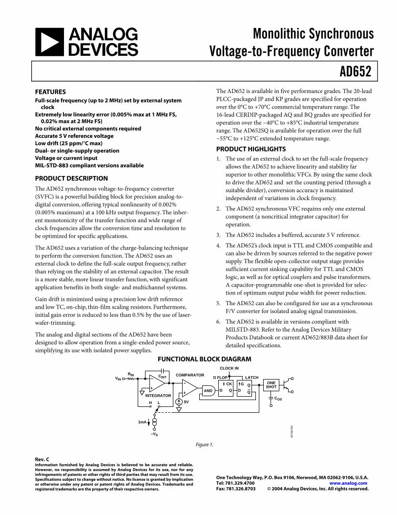
FUNCTIONAL BLOCK DIAGRAM
COMPARATOR
AND
CKQD
G QD Q
D FLOP LATCH
CLOCK IN
ONESHOT
COS5V
CINTRIN
INTEGRATOR
H L
1mA
–VS
VIN
0079
8-00
1
Figure 1.
AD652
Rev. C | Page 2 of 28
TABLE OF CONTENTS Specifications..................................................................................... 3
Absolute Maximum Ratings............................................................ 5
ESD Caution.................................................................................. 5
Definitions of Specifications ....................................................... 5
Theory of Operation ........................................................................ 6
Overrange ...................................................................................... 8
SVFC Connection for Dual Supply, Positive Input Voltages .. 9
SVFC Connections for Negative Input Voltages ...................... 9
SVFC Connection for Bipolar Input Voltages ........................ 10
PLCC Connections..................................................................... 11
Gain and Offset Calibration...................................................... 11
Gain Performance ...................................................................... 12
Reference Noise .......................................................................... 12
Digital Interfacing Considerations........................................... 12
Component Selection ................................................................ 12
Digital Ground............................................................................ 13
Single-Supply Operation ........................................................... 14
Frequency-to-Voltage Converter ............................................. 15
Decoupling and Grounding...................................................... 16
Frequency Output Multiplier.................................................... 17
Single-Line Multiplexed Data Transmission .......................... 18
Isolated Front End...................................................................... 22
A-to-D Conversion .................................................................... 22
Delta Modulator ......................................................................... 23
Bridge Transducer Interface...................................................... 24
Outline Dimensions ....................................................................... 25
Ordering Guide............................................................................... 26
REVISION HISTORY
5/04—Data Sheet Changed from Rev. B to Rev. C
Updated Format..............................................................Universal Changes to Gain and Offset Calibration section.................... 11 Updated Outline Dimensions ................................................... 25 Changes to Ordering Guide ...................................................... 26
2/00—Data Sheet Changed from Rev. A to Rev. B
AD652
Rev. C | Page 3 of 28
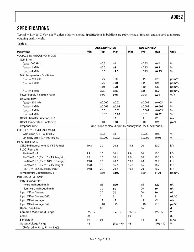
SPECIFICATIONS Typical @ TA = 25°C, VS = ±15 V, unless otherwise noted. Specifications in boldface are 100% tested at final test and are used to measure outgoing quality levels.
Table 1. AD652JP/AQ/SQ AD652KP/BQ Parameter Min Typ Max Min Typ Max Unit VOLTAGE-TO-FREQUENCY MODE
Gain Error fCLOCK= 200 kHz ±0.5 ±1 ±0.25 ±0.5 % fCLOCK = 1 MHz ±0.5 ±1 ±0.25 ±0.5 % fCLOCK = 4 MHz ±0.5 ±1.5 ±0.25 ±0.75 %
Gain Temperature Coefficient fCLOCK = 200 kHz ±25 ±50 ±15 ±25 ppm/°C fCLOCK = 1 MHz ±25 ±50 ±15 ±25 ppm/°C ±10 ±50 ±10 ±30 ppm/°C1
fCLOCK = 4 MHz ±25 ±75 ±15 ±50 ppm/°C Power Supply Rejection Ratio 0.001 0.01 0.001 0.01 %/V Linearity Error
fCLOCK = 200 kHz ±0.002 ±0.02 ±0.002 ±0.005 % fCLOCK = 1 MHz ±0.002 ±0.02 ±0.002 ±0.005 % fCLOCK = 2 MHz ±0.01 ±0.02 ±0.002 ±0.005 % fCLOCK = 4 MHz ±0.02 ±0.05 ±0.01 ±0.02 %
Offset (Transfer Function, RTI) ± 1 ±3 ±1 ±2 mV Offset Temperature Coefficient ±10 ±50 ±10 ±25 µV/°C Response Time One Period of New Output Frequency Plus One Clock Period.
FREQUENCY-TO-VOLTAGE MODE Gain Error, fIN = 100 kHz FS ±0.5 ±1 ±0.25 ±0.5 % Linearity Error, fIN = 100 kHz FS ±0.002 ±0.02 ±0.002 ±0.01 %
INPUT RESISTORS CERDIP (Figure 2)(0 to 10 V FS Range) 19.8 20 20.2 19.8 20 20.2 kΩ PLCC (Figure 3)
Pin 8 to Pin 7 9.9 10 10.1 9.9 10 10.1 kΩ Pin 7 to Pin 5 (0 V to 5 V FS Range) 9.9 10 10.1 9.9 10 10.1 kΩ Pin 8 to Pin 5 (0 V to 10 V FS Range) 19.8 20 20.2 19.8 20 20.2 kΩ Pin 9 to Pin 5 (0 V to 8 V FS Range) 15.8 16 16.2 15.8 16 16.2 kΩ Pin 10 to Pin 5 (Auxiliary Input) 19.8 20 20.2 19.8 20 20.2 kΩ
Temperature Coefficient (All) ±50 ±100 ±50 ±100 ppm/°C
INTEGRATOR OP AMP Input Bias Current
Inverting Input (Pin 5) ±5 ±20 ±5 ±20 nA Noninverting Input (Pin 6) 20 50 20 50 nA
Input Offset Current 20 70 20 70 nA Input Offset Current Drift 1 3 1 2 nA/°C Input Offset Voltage ±1 ±3 ±1 ±2 mV Input Offset Voltage Drift ±10 ±25 ±10 ±15 µV/°C Open-Loop Gain 86 86 dB Common-Mode Input Range –VS + 5 +VS – 5 –VS + 5 +VS – 5 V CMRR 80 80 dB Bandwidth 14 95 14 95 MHz Output Voltage Range −1 (+VS − 4) −1 (+VS − 4) V
(Referred to Pin 6, R1 > = 5 kΩ)
AD652
Rev. C | Page 4 of 28
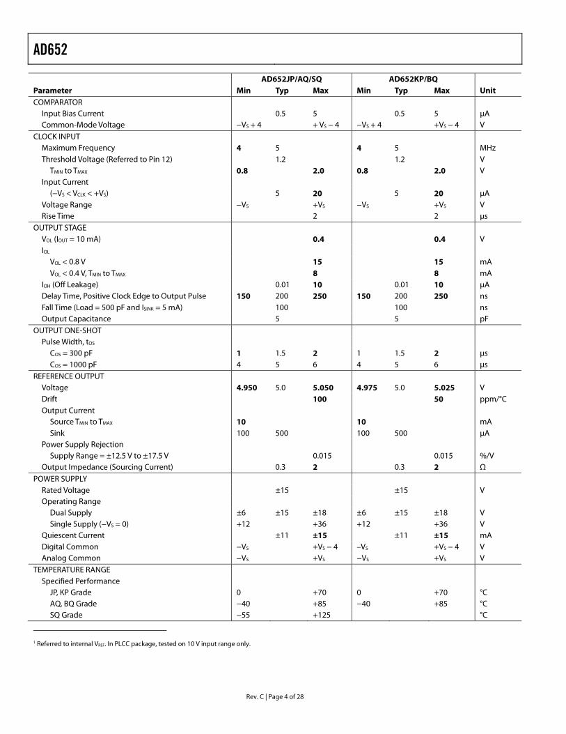
AD652JP/AQ/SQ AD652KP/BQ Parameter Min Typ Max Min Typ Max Unit COMPARATOR
Input Bias Current 0.5 5 0.5 5 µA Common-Mode Voltage −VS + 4 + VS − 4 −VS + 4 +VS − 4 V
CLOCK INPUT Maximum Frequency 4 5 4 5 MHz Threshold Voltage (Referred to Pin 12) 1.2 1.2 V
TMIN to TMAX 0.8 2.0 0.8 2.0 V Input Current
(−VS < VCLK < +VS) 5 20 5 20 µA Voltage Range −VS +VS −VS +VS V Rise Time 2 2 µs
OUTPUT STAGE VOL (IOUT = 10 mA) 0.4 0.4 V IOL
VOL < 0.8 V 15 15 mA VOL < 0.4 V, TMIN to TMAX 8 8 mA
IOH (Off Leakage) 0.01 10 0.01 10 µA Delay Time, Positive Clock Edge to Output Pulse 150 200 250 150 200 250 ns Fall Time (Load = 500 pF and ISINK = 5 mA) 100 100 ns Output Capacitance 5 5 pF
OUTPUT ONE-SHOT Pulse Width, tOS
COS = 300 pF 1 1.5 2 1 1.5 2 µs COS = 1000 pF 4 5 6 4 5 6 µs
REFERENCE OUTPUT Voltage 4.950 5.0 5.050 4.975 5.0 5.025 V Drift 100 50 ppm/°C Output Current
Source TMIN to TMAX 10 10 mA Sink 100 500 100 500 µA
Power Supply Rejection Supply Range = ±12.5 V to ±17.5 V 0.015 0.015 %/V
Output Impedance (Sourcing Current) 0.3 2 0.3 2 Ω
POWER SUPPLY Rated Voltage ±15 ±15 V Operating Range
Dual Supply ±6 ±15 ±18 ±6 ±15 ±18 V Single Supply (−VS = 0) +12 +36 +12 +36 V
Quiescent Current ±11 ±15 ±11 ±15 mA Digital Common −VS +VS − 4 –VS +VS − 4 V Analog Common −VS +VS −VS +VS V
TEMPERATURE RANGE Specified Performance
JP, KP Grade 0 +70 0 +70 °C AQ, BQ Grade −40 +85 −40 +85 °C SQ Grade −55 +125 °C
1 Referred to internal VREF. In PLCC package, tested on 10 V input range only.
AD652
Rev. C | Page 5 of 28
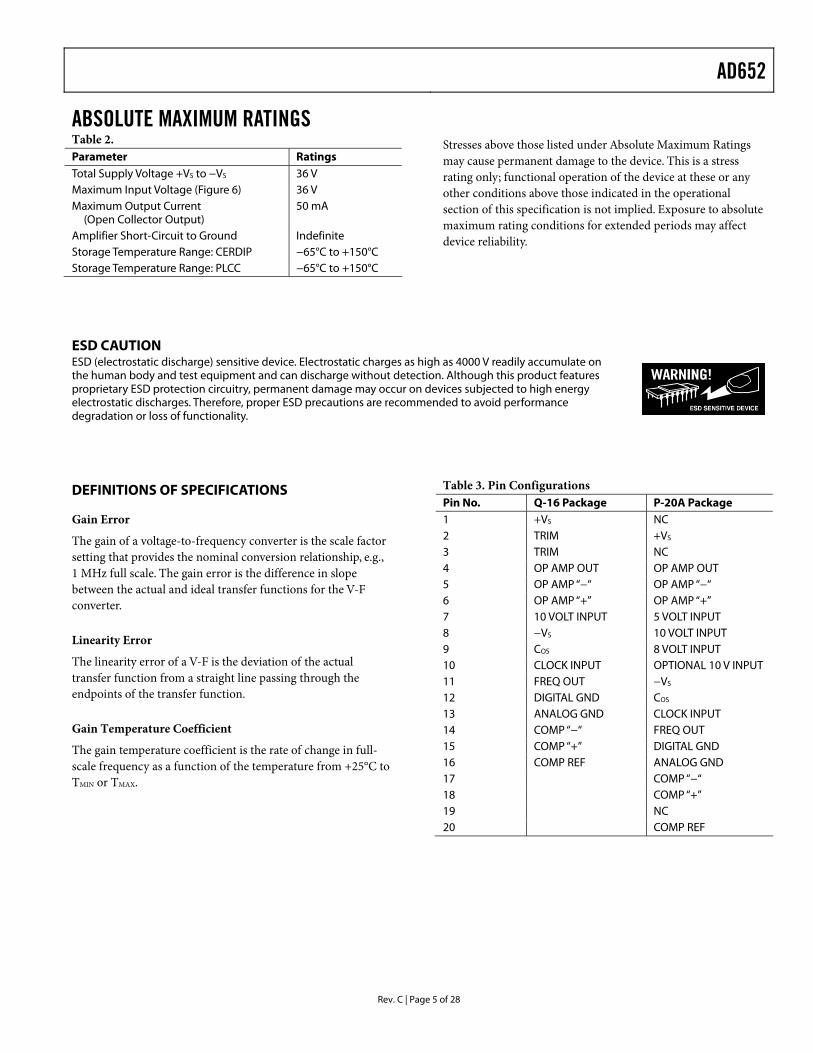
ABSOLUTE MAXIMUM RATINGS Table 2. Parameter Ratings Total Supply Voltage +VS to −VS 36 V Maximum Input Voltage (Figure 6) 36 V Maximum Output Current
(Open Collector Output) 50 mA
Amplifier Short-Circuit to Ground Indefinite Storage Temperature Range: CERDIP −65°C to +150°C Storage Temperature Range: PLCC −65°C to +150°C
Stresses above those listed under Absolute Maximum Ratings may cause permanent damage to the device. This is a stress rating only; functional operation of the device at these or any other conditions above those indicated in the operational section of this specification is not implied. Exposure to absolute maximum rating conditions for extended periods may affect device reliability.
ESD CAUTION ESD (electrostatic discharge) sensitive device. Electrostatic charges as high as 4000 V readily accumulate on the human body and test equipment and can discharge without detection. Although this product features proprietary ESD protection circuitry, permanent damage may occur on devices subjected to high energy electrostatic discharges. Therefore, proper ESD precautions are recommended to avoid performance degradation or loss of functionality.
DEFINITIONS OF SPECIFICATIONS
Gain Error
The gain of a voltage-to-frequency converter is the scale factor setting that provides the nominal conversion relationship, e.g., 1 MHz full scale. The gain error is the difference in slope between the actual and ideal transfer functions for the V-F converter.
Linearity Error
The linearity error of a V-F is the deviation of the actual transfer function from a straight line passing through the endpoints of the transfer function.
Gain Temperature Coefficient
The gain temperature coefficient is the rate of change in full-scale frequency as a function of the temperature from +25°C to TMIN or TMAX.
Table 3. Pin Configurations Pin No. Q-16 Package P-20A Package 1 +VS NC 2 TRIM +VS
3 TRIM NC 4 OP AMP OUT OP AMP OUT 5 OP AMP “−“ OP AMP “−“ 6 OP AMP “+” OP AMP “+” 7 10 VOLT INPUT 5 VOLT INPUT 8 −VS 10 VOLT INPUT 9 COS 8 VOLT INPUT 10 CLOCK INPUT OPTIONAL 10 V INPUT 11 FREQ OUT −VS
12 DIGITAL GND COS
13 ANALOG GND CLOCK INPUT 14 COMP “−“ FREQ OUT 15 COMP “+” DIGITAL GND 16 COMP REF ANALOG GND 17 COMP “−“ 18 COMP “+” 19 NC 20 COMP REF
AD652
Rev. C | Page 6 of 28
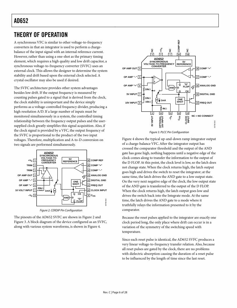
THEORY OF OPERATION A synchronous VFC is similar to other voltage-to-frequency converters in that an integrator is used to perform a charge-balance of the input signal with an internal reference current. However, rather than using a one-shot as the primary timing element, which requires a high quality and low drift capacitor, a synchronous voltage-to-frequency converter (SVFC) uses an external clock. This allows the designer to determine the system stability and drift based upon the external clock selected. A crystal oscillator may also be used if desired.
The SVFC architecture provides other system advantages besides low drift. If the output frequency is measured by counting pulses gated to a signal that is derived from the clock, the clock stability is unimportant and the device simply performs as a voltage-controlled frequency divider, producing a high resolution A/D. If a large number of inputs must be monitored simultaneously in a system, the controlled timing relationship between the frequency output pulses and the user-supplied clock greatly simplifies this signal acquisition. Also, if the clock signal is provided by a VFC, the output frequency of the SVFC is proportional to the product of the two input voltages. Therefore, multiplication and A-to-D conversion on two signals are performed simultaneously.
0079
8-00
2
+VS 1
TRIM 2
TRIM 3
OP AMP OUT 4
OP AMP "–" 5
OP AMP "+" 6
10 VOLT INPUT 7
–VS 8
COMP REF16
COMP "+"15
COMP "–"14
ANALOG GND13
DIGITAL GND12
FREQ OUT11
CLOCK INPUT10
COS9
ONESHOT
AND "D"FLOP
Q CKD
Q
1mA20kΩ
AD652SYNCHRONOUS
VOLTAGE-TO-FREQUENCYCONVERTER
5VREFERENCE
Figure 2. CERDIP Pin Configuration
The pinouts of the AD652 SVFC are shown in Figure 2 and Figure 3. A block diagram of the device configured as an SVFC, along with various system waveforms, is shown in Figure 4.
0079
8-00
3
OP AMP OUT 4
OP AMP "–" 5
OP AMP "+" 6
5V INPUT 7
10V INPUT 8
COMP "+"18
COMP "–"17
ANALOG GND16
DIGITAL GND15
FREQ OUT14
8V IN
PUT
9
OPT
ION
AL
10V
INPU
T
10
–VS
11
CO
S
12
CLO
CK
INPU
T
13
NC
3
+VS
2
NC
1
CO
MP
REF
20
NC
19
1mA
5VREFERENCE
NC = NO CONNECT
AND"D"
FLOPQ
CKD
Q
ONESHOT
10kΩ
10kΩ16kΩ
4kΩ
AD652SYNCHRONOUS
VOLTAGE-TO-FREQUENCYCONVERTER
Figure 3. PLCC Pin Configuration
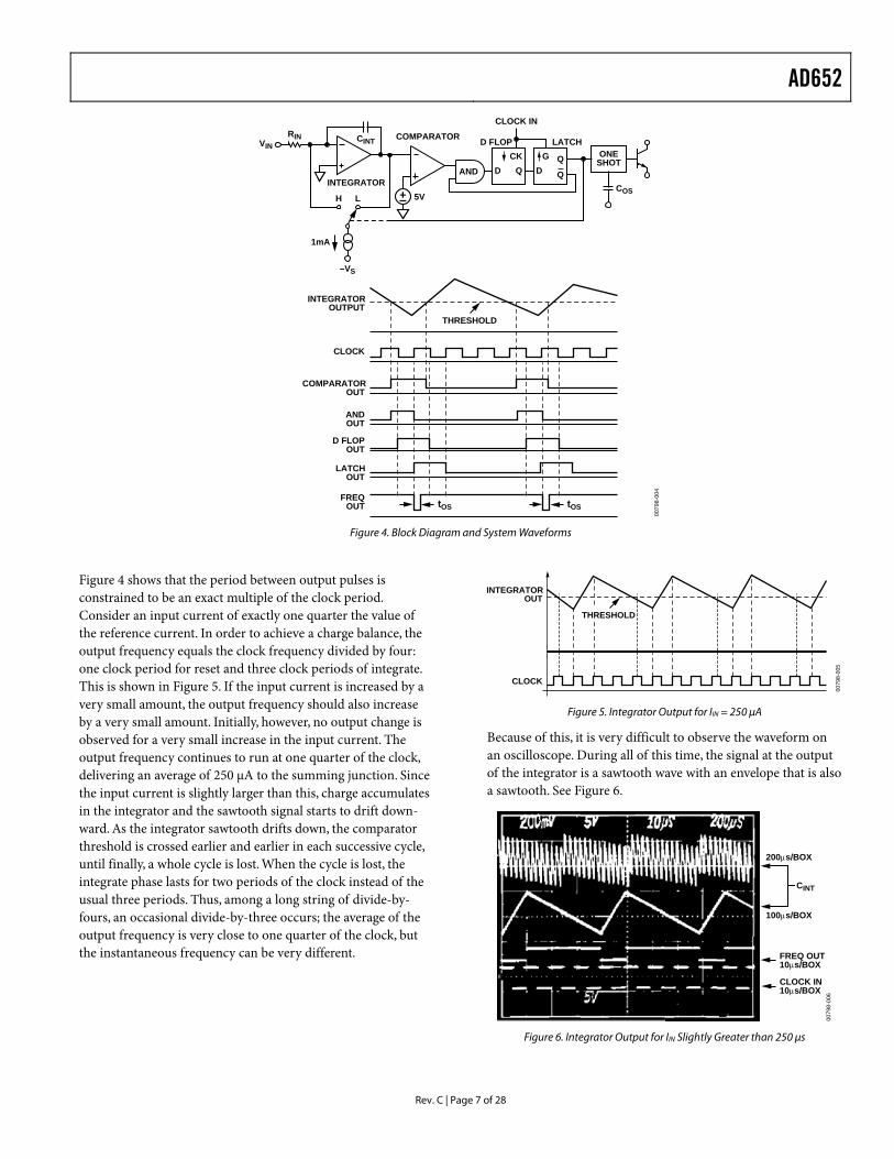
Figure 4 shows the typical up-and-down ramp integrator output of a charge-balance VFC. After the integrator output has crossed the comparator threshold and the output of the AND gate has gone high, nothing happens until a negative edge of the clock comes along to transfer the information to the output of the D FLOP. At this point, the clock level is low, so the latch does not change state. When the clock returns high, the latch output goes high and drives the switch to reset the integrator; at the same time, the latch drives the AND gate to a low output state. On the very next negative edge of the clock, the low output state of the AND gate is transferred to the output of the D FLOP. When the clock returns high, the latch output goes low and drives the switch back into the Integrate mode. At the same time, the latch drives the AND gate to a mode where it truthfully relays the information presented to it by the comparator.
Because the reset pulses applied to the integrator are exactly one clock period long, the only place where drift can occur is in a variation of the symmetry of the switching speed with temperature.
Since each reset pulse is identical, the AD652 SVFC produces a very linear voltage-to-frequency transfer relation. Also, because all reset pulses are gated by the clock, there are no problems with dielectric absorption causing the duration of a reset pulse to be influenced by the length of time since the last reset.
AD652
Rev. C | Page 7 of 28
0079
8-00
4
COMPARATOR
AND
CKQD
G QD Q
D FLOP LATCH
CLOCK IN
ONESHOT
COS5V
CINTRIN
INTEGRATOR
H L
1mA
–VS
VIN
tOS tOS
INTEGRATOROUTPUT
THRESHOLD
CLOCK
COMPARATOROUT
ANDOUT
D FLOPOUT
LATCHOUT
FREQOUT
Figure 4. Block Diagram and System Waveforms
Figure 4 shows that the period between output pulses is constrained to be an exact multiple of the clock period. Consider an input current of exactly one quarter the value of the reference current. In order to achieve a charge balance, the output frequency equals the clock frequency divided by four: one clock period for reset and three clock periods of integrate. This is shown in Figure 5. If the input current is increased by a very small amount, the output frequency should also increase by a very small amount. Initially, however, no output change is observed for a very small increase in the input current. The output frequency continues to run at one quarter of the clock, delivering an average of 250 µA to the summing junction. Since the input current is slightly larger than this, charge accumulates in the integrator and the sawtooth signal starts to drift down-ward. As the integrator sawtooth drifts down, the comparator threshold is crossed earlier and earlier in each successive cycle, until finally, a whole cycle is lost. When the cycle is lost, the integrate phase lasts for two periods of the clock instead of the usual three periods. Thus, among a long string of divide-by-fours, an occasional divide-by-three occurs; the average of the output frequency is very close to one quarter of the clock, but the instantaneous frequency can be very different.
0079
8-00
5
INTEGRATOROUT
CLOCK
THRESHOLD
Figure 5. Integrator Output for IIN = 250 µA
Because of this, it is very difficult to observe the waveform on an oscilloscope. During all of this time, the signal at the output of the integrator is a sawtooth wave with an envelope that is also a sawtooth. See Figure 6.
200µs/BOX
100µs/BOX
CINT
FREQ OUT10µs/BOX
CLOCK IN10µs/BOX
0079
8-00
6
Figure 6. Integrator Output for IIN Slightly Greater than 250 µs
AD652
Rev. C | Page 8 of 28
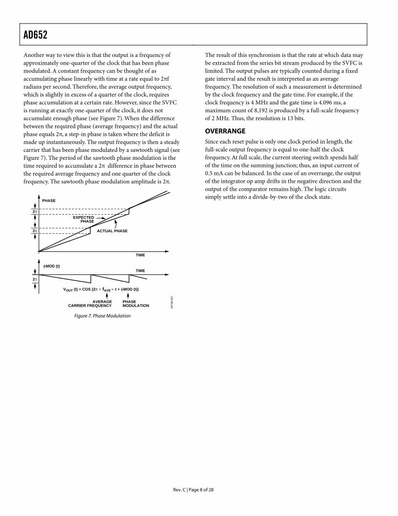
Another way to view this is that the output is a frequency of approximately one-quarter of the clock that has been phase modulated. A constant frequency can be thought of as accumulating phase linearly with time at a rate equal to 2πf radians per second. Therefore, the average output frequency, which is slightly in excess of a quarter of the clock, requires phase accumulation at a certain rate. However, since the SVFC is running at exactly one-quarter of the clock, it does not accumulate enough phase (see Figure 7). When the difference between the required phase (average frequency) and the actual phase equals 2π, a step-in phase is taken where the deficit is made up instantaneously. The output frequency is then a steady carrier that has been phase modulated by a sawtooth signal (see Figure 7). The period of the sawtooth phase modulation is the time required to accumulate a 2π difference in phase between the required average frequency and one quarter of the clock frequency. The sawtooth phase modulation amplitude is 2π.
0079
8-00
7
TIME
TIMEφMOD (t)
ACTUAL PHASE
EXPECTEDPHASE
PHASE
2π
2π
2π
PHASEMODULATION
AVERAGECARRIER FREQUENCY
VOUT (t) = COS (2π × fAVE × t + φMOD (t))
Figure 7. Phase Modulation
The result of this synchronism is that the rate at which data may be extracted from the series bit stream produced by the SVFC is limited. The output pulses are typically counted during a fixed gate interval and the result is interpreted as an average frequency. The resolution of such a measurement is determined by the clock frequency and the gate time. For example, if the clock frequency is 4 MHz and the gate time is 4.096 ms, a maximum count of 8,192 is produced by a full-scale frequency of 2 MHz. Thus, the resolution is 13 bits.
OVERRANGE Since each reset pulse is only one clock period in length, the full-scale output frequency is equal to one-half the clock frequency. At full scale, the current steering switch spends half of the time on the summing junction; thus, an input current of 0.5 mA can be balanced. In the case of an overrange, the output of the integrator op amp drifts in the negative direction and the output of the comparator remains high. The logic circuits simply settle into a divide-by-two of the clock state.
AD652
Rev. C | Page 9 of 28
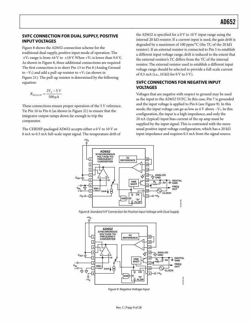
SVFC CONNECTION FOR DUAL SUPPLY, POSITIVE INPUT VOLTAGES Figure 8 shows the AD652 connection scheme for the traditional dual supply, positive input mode of operation. The ±VS range is from ±6 V to ±18 V. When +VS is lower than 9.0 V, As shown in Figure 8, three additional connections are required The first connection is to short Pin 13 to Pin 8 (Analog Ground to −VS) and add a pull-up resistor to +VS (as shown in Figure 21). The pull-up resistor is determined by the following equation:
µA500V52 −
= SPULLUP
VR
These connections ensure proper operation of the 5 V reference. Tie Pin 16 to Pin 6 (as shown in Figure 21) to ensure that the integrator output ramps down far enough to trip the comparator.
The CERDIP-packaged AD652 accepts either a 0 V to 10 V or 0 mA to 0.5 mA full-scale input signal. The temperature drift of
the AD652 is specified for a 0 V to 10 V input range using the internal 20 kΩ resistor. If a current input is used, the gain drift is degraded by a maximum of 100 ppm/°C (the TC of the 20 kΩ resistor). If an external resistor is connected to Pin 5 to establish a different input voltage range, drift is induced to the extent that the external resistor’s TC differs from the TC of the internal resistor. The external resistor used to establish a different input voltage range should be selected to provide a full-scale current of 0.5 mA (i.e., 10 kΩ for 0 V to 5 V).
SVFC CONNECTIONS FOR NEGATIVE INPUT VOLTAGES Voltages that are negative with respect to ground may be used as the input to the AD652 SVFC. In this case, Pin 7 is grounded and the input voltage is applied to Pin 6 (see Figure 9). In this mode, the input voltage can go as low as 4 V above −VS. In this configuration, the input is a high impedance, and only the 20 nA (typical) input bias current of the op amp must be supplied by the input signal. This is contrasted with the more usual positive input voltage configuration, which has a 20 kΩ input impedance and requires 0.5 mA from the signal source.
0079
8-00
8
+VS
1
2
3
4
–
+
5
6
7
+VS
VIN
8
16
15
14
13
12
11
10
9
ONESHOT
AND "D"FLOP
Q CKD
Q
1mA20kΩ
AD652SYNCHRONOUS
VOLTAGE-TO-FREQUENCYCONVERTER
5VREFERENCE
RL 5V
CLOCK
ANALOGGND
DIGITALGNDFREQOUT
CINT
–VS
Figure 8. Standard V/F Connection for Positive Input Voltage with Dual Supply
0079
8-00
9
+VS
1
2
3
4
5
6
7
+VS
–VS
8
16
15
14
13
12
11
10
9
ONESHOT
AND "D"FLOP
Q CKD
Q
1mA20kΩ
AD652SYNCHRONOUS
VOLTAGE-TO-FREQUENCYCONVERTER
5VREFERENCE
RL 5V
CLOCK
ANALOGGND
DIGITALGNDFREQOUT
CINT
–
+VIN
Figure 9. Negative Voltage Input
AD652
Rev. C | Page 10 of 28
0079
8-01
0
+VS
1
2
3
4
5
6
7
–VS
8
16
15
14
13
12
11
10
9
ONESHOT
AND "D"FLOP
Q CKD
Q
1mA20kΩ
20kΩ
AD652SYNCHRONOUS
VOLTAGE-TO-FREQUENCYCONVERTER
5VREFERENCE
RL 5V
CLOCK
COS
ANALOGGND
DIGITALGNDFREQOUT
CINT
VIN
±5V
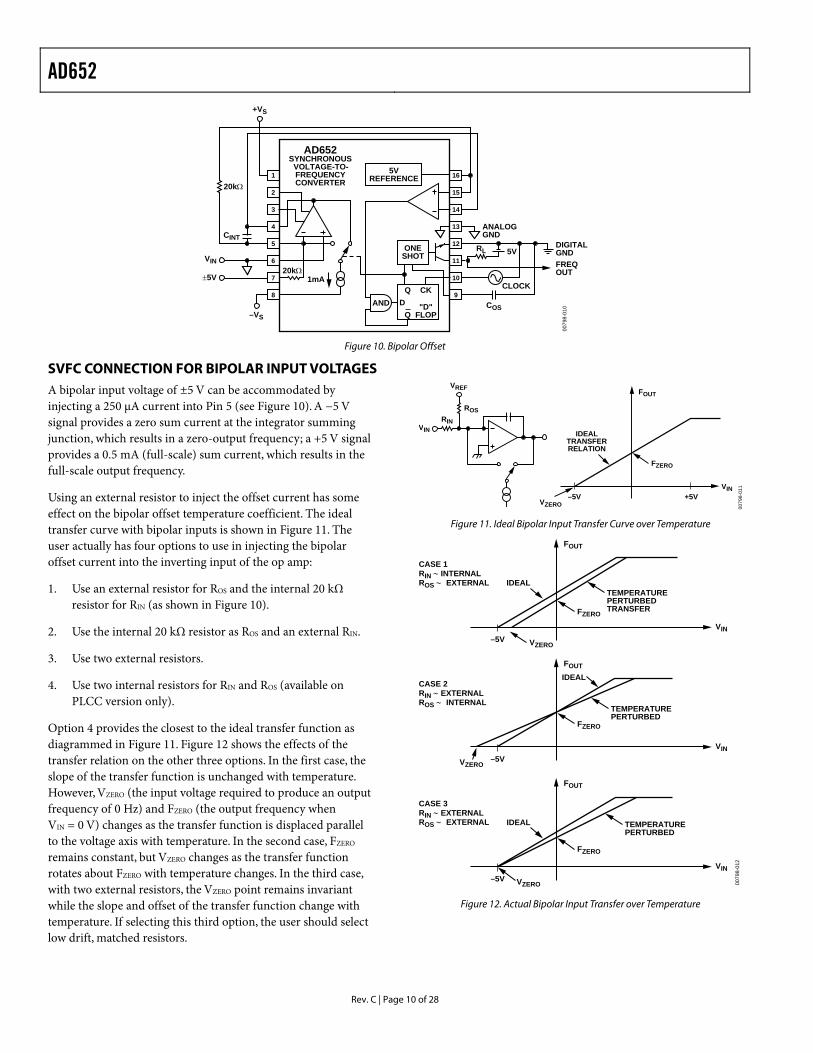
Figure 10. Bipolar Offset
SVFC CONNECTION FOR BIPOLAR INPUT VOLTAGES A bipolar input voltage of ±5 V can be accommodated by injecting a 250 µA current into Pin 5 (see Figure 10). A −5 V signal provides a zero sum current at the integrator summing junction, which results in a zero-output frequency; a +5 V signal provides a 0.5 mA (full-scale) sum current, which results in the full-scale output frequency.
Using an external resistor to inject the offset current has some effect on the bipolar offset temperature coefficient. The ideal transfer curve with bipolar inputs is shown in Figure 11. The user actually has four options to use in injecting the bipolar offset current into the inverting input of the op amp:
1. Use an external resistor for ROS and the internal 20 kΩ resistor for RIN (as shown in Figure 10).
2. Use the internal 20 kΩ resistor as ROS and an external RIN.
3. Use two external resistors.
4. Use two internal resistors for RIN and ROS (available on PLCC version only).
Option 4 provides the closest to the ideal transfer function as diagrammed in Figure 11. Figure 12 shows the effects of the transfer relation on the other three options. In the first case, the slope of the transfer function is unchanged with temperature. However, VZERO (the input voltage required to produce an output frequency of 0 Hz) and FZERO (the output frequency when VIN = 0 V) changes as the transfer function is displaced parallel to the voltage axis with temperature. In the second case, FZERO remains constant, but VZERO changes as the transfer function rotates about FZERO with temperature changes. In the third case, with two external resistors, the VZERO point remains invariant while the slope and offset of the transfer function change with temperature. If selecting this third option, the user should select low drift, matched resistors.
0079
8-01
1
VREF
VIN
ROSRIN
IDEALTRANSFERRELATION
VZERO
FOUT
FZERO
–5V +5VVIN
Figure 11. Ideal Bipolar Input Transfer Curve over Temperature
0079
8-01
2
IDEAL
FOUT
FZERO
VIN
TEMPERATUREPERTURBEDTRANSFER
VZERO–5V
CASE 1RIN ∼ INTERNALROS ∼ EXTERNAL
IDEALFOUT
FZERO
VIN
TEMPERATUREPERTURBED
VZERO–5V
CASE 2RIN ∼ EXTERNALROS ∼ INTERNAL
IDEAL
FOUT
FZERO
VIN
TEMPERATUREPERTURBED
VZERO–5V
CASE 3RIN ∼ EXTERNALROS ∼ EXTERNAL
Figure 12. Actual Bipolar Input Transfer over Temperature
AD652
Rev. C | Page 11 of 28
0079
8-01
3
NC = NO CONNECT
5
7
8
NC
VIN+
– NC NC
6
9 10
AD652SYNCHRONOUSVOLTAGE-TO-FREQUENCYCONVERTER
10kΩ
10kΩ16kΩ
4kΩ
A. PLCC 0V TO 10V INPUT
5
7
8
NC
NC
NC
6
9 10
AD652SYNCHRONOUSVOLTAGE-TO-FREQUENCYCONVERTER
10kΩ
10kΩ16kΩ
4kΩ
B. PLCC 0V TO 8V INPUT
VIN+
–
5
7
8NC
NC NC
6
9 10
AD652SYNCHRONOUSVOLTAGE-TO-FREQUENCYCONVERTER
10kΩ
10kΩ16kΩ
4kΩ
C. PLCC 0V TO 5V INPUT
VIN+
–
5
7
8
NC
VIN±5V
NC
6
9 10
AD652SYNCHRONOUSVOLTAGE-TO-FREQUENCYCONVERTER
10kΩ
10kΩ16kΩ
4kΩ
D. PLCC ±5V INPUT
5V REF
20
Figure 13.
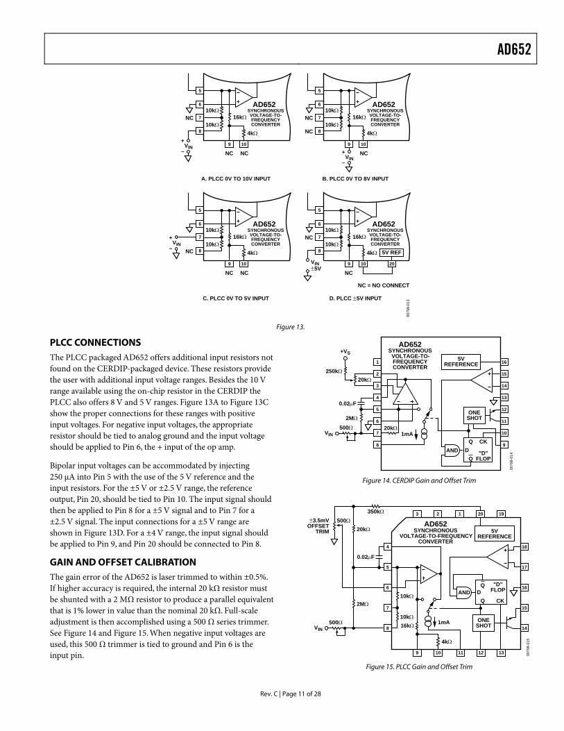
PLCC CONNECTIONS The PLCC packaged AD652 offers additional input resistors not found on the CERDIP-packaged device. These resistors provide the user with additional input voltage ranges. Besides the 10 V range available using the on-chip resistor in the CERDIP the PLCC also offers 8 V and 5 V ranges. Figure 13A to Figure 13C show the proper connections for these ranges with positive input voltages. For negative input voltages, the appropriate resistor should be tied to analog ground and the input voltage should be applied to Pin 6, the + input of the op amp.
Bipolar input voltages can be accommodated by injecting 250 µA into Pin 5 with the use of the 5 V reference and the input resistors. For the ±5 V or ±2.5 V range, the reference output, Pin 20, should be tied to Pin 10. The input signal should then be applied to Pin 8 for a ±5 V signal and to Pin 7 for a ±2.5 V signal. The input connections for a ±5 V range are shown in Figure 13D. For a ±4 V range, the input signal should be applied to Pin 9, and Pin 20 should be connected to Pin 8.
GAIN AND OFFSET CALIBRATION The gain error of the AD652 is laser trimmed to within ±0.5%. If higher accuracy is required, the internal 20 kΩ resistor must be shunted with a 2 MΩ resistor to produce a parallel equivalent that is 1% lower in value than the nominal 20 kΩ. Full-scale adjustment is then accomplished using a 500 Ω series trimmer. See Figure 14 and Figure 15. When negative input voltages are used, this 500 Ω trimmer is tied to ground and Pin 6 is the input pin.
0079
8-01
4
1
2
3
4
5
6
7
8
16
15
14
13
12
11
10
9
ONESHOT
AND "D"FLOP
Q CKD
Q
1mA20kΩ
AD652SYNCHRONOUS
VOLTAGE-TO-FREQUENCYCONVERTER
5VREFERENCE
VIN
+VS
0.02µF
2MΩ
500Ω
250kΩ20kΩ
Figure 14. CERDIP Gain and Offset Trim
0079
8-01
5
4
5
6
7
8
18
17
16
15
14
9 10 11 12 13
3 2 1 20 19
1mA
5VREFERENCE
AD652
AND"D"
FLOPQ
CKD
Q
ONESHOT
10kΩ
10kΩ16kΩ
4kΩ
SYNCHRONOUSVOLTAGE-TO-FREQUENCY
CONVERTER
VIN500Ω
500Ω
2MΩ
0.02µF
20kΩ
350kΩ±3.5mV
OFFSETTRIM
Figure 15. PLCC Gain and Offset Trim
AD652
Rev. C | Page 12 of 28
This gain trim should be done with an input voltage of 9 V, and the output frequency should be adjusted to exactly 45% of the clock frequency. Since the device settles into a divide-by-2 mode for an input overrange condition, adjusting the gain with a 10 V input is impractical; the output frequency is exactly one-half the clock frequency if the gain is too high and does not change with adjustment until the exact proper scale factor was achieved. Thus, the gain adjustment should be done with a 9 V input.
The offset of the op amp may be trimmed to zero with the trim scheme shown in Figure 14 for the CERDIP package and Figure 15 for the PLCC package. One way of trimming the offset is by grounding Pin 7 (8) of the CERDIP (PLCC) device and observing the waveform at Pin 4. If the offset voltage of the op amp is positive, the integrator has saturated and the voltage is at the positive rail. If the offset voltage is negative, there is a small effective input current that causes the AD652 to oscillate; a sawtooth waveform is observed at Pin 4. The potentiometer should be adjusted until the downward slope of this sawtooth becomes very slow, down to a frequency of 1 Hz or less. In an analog-to-digital conversion application, an easier way to trim the offset is to apply a small input voltage, such as 0.01% of the full-scale voltage, and adjust the potentiometer until the correct digital output is reached.
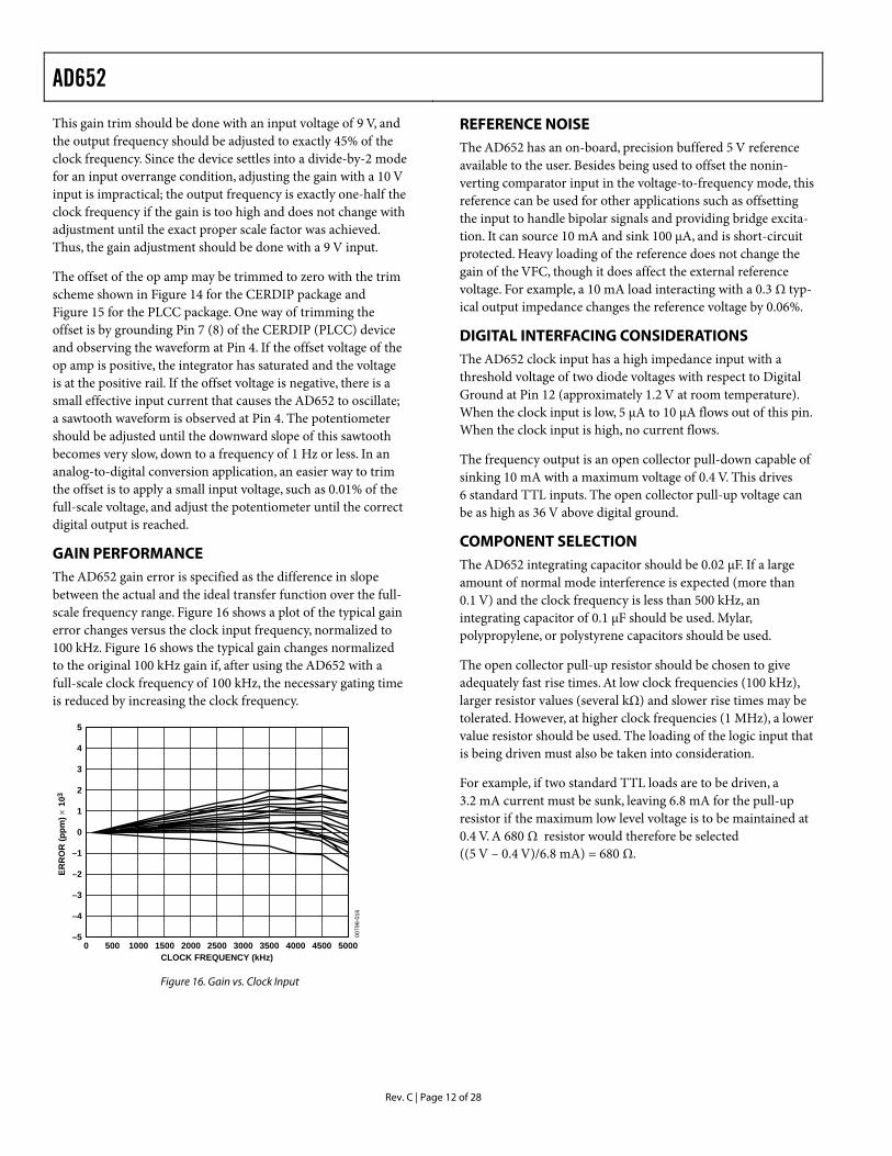
GAIN PERFORMANCE The AD652 gain error is specified as the difference in slope between the actual and the ideal transfer function over the full-scale frequency range. Figure 16 shows a plot of the typical gain error changes versus the clock input frequency, normalized to 100 kHz. Figure 16 shows the typical gain changes normalized to the original 100 kHz gain if, after using the AD652 with a full-scale clock frequency of 100 kHz, the necessary gating time is reduced by increasing the clock frequency.
5
–5
–4
–3
–2
–1
0
1
2
3
4
0 500 1000 1500 2000 2500 3000 3500 4000 4500 5000
0079
8-01
6
CLOCK FREQUENCY (kHz)
ERR
OR
(ppm
)×10
3
Figure 16. Gain vs. Clock Input
REFERENCE NOISE The AD652 has an on-board, precision buffered 5 V reference available to the user. Besides being used to offset the nonin-verting comparator input in the voltage-to-frequency mode, this reference can be used for other applications such as offsetting the input to handle bipolar signals and providing bridge excita-tion. It can source 10 mA and sink 100 µA, and is short-circuit protected. Heavy loading of the reference does not change the gain of the VFC, though it does affect the external reference voltage. For example, a 10 mA load interacting with a 0.3 Ω typ-ical output impedance changes the reference voltage by 0.06%.
DIGITAL INTERFACING CONSIDERATIONS The AD652 clock input has a high impedance input with a threshold voltage of two diode voltages with respect to Digital Ground at Pin 12 (approximately 1.2 V at room temperature). When the clock input is low, 5 µA to 10 µA flows out of this pin. When the clock input is high, no current flows.
The frequency output is an open collector pull-down capable of sinking 10 mA with a maximum voltage of 0.4 V. This drives 6 standard TTL inputs. The open collector pull-up voltage can be as high as 36 V above digital ground.
COMPONENT SELECTION The AD652 integrating capacitor should be 0.02 µF. If a large amount of normal mode interference is expected (more than 0.1 V) and the clock frequency is less than 500 kHz, an integrating capacitor of 0.1 µF should be used. Mylar, polypropylene, or polystyrene capacitors should be used.
The open collector pull-up resistor should be chosen to give adequately fast rise times. At low clock frequencies (100 kHz), larger resistor values (several kΩ) and slower rise times may be tolerated. However, at higher clock frequencies (1 MHz), a lower value resistor should be used. The loading of the logic input that is being driven must also be taken into consideration.
For example, if two standard TTL loads are to be driven, a 3.2 mA current must be sunk, leaving 6.8 mA for the pull-up resistor if the maximum low level voltage is to be maintained at 0.4 V. A 680 Ω resistor would therefore be selected ((5 V – 0.4 V)/6.8 mA) = 680 Ω.
AD652
Rev. C | Page 13 of 28
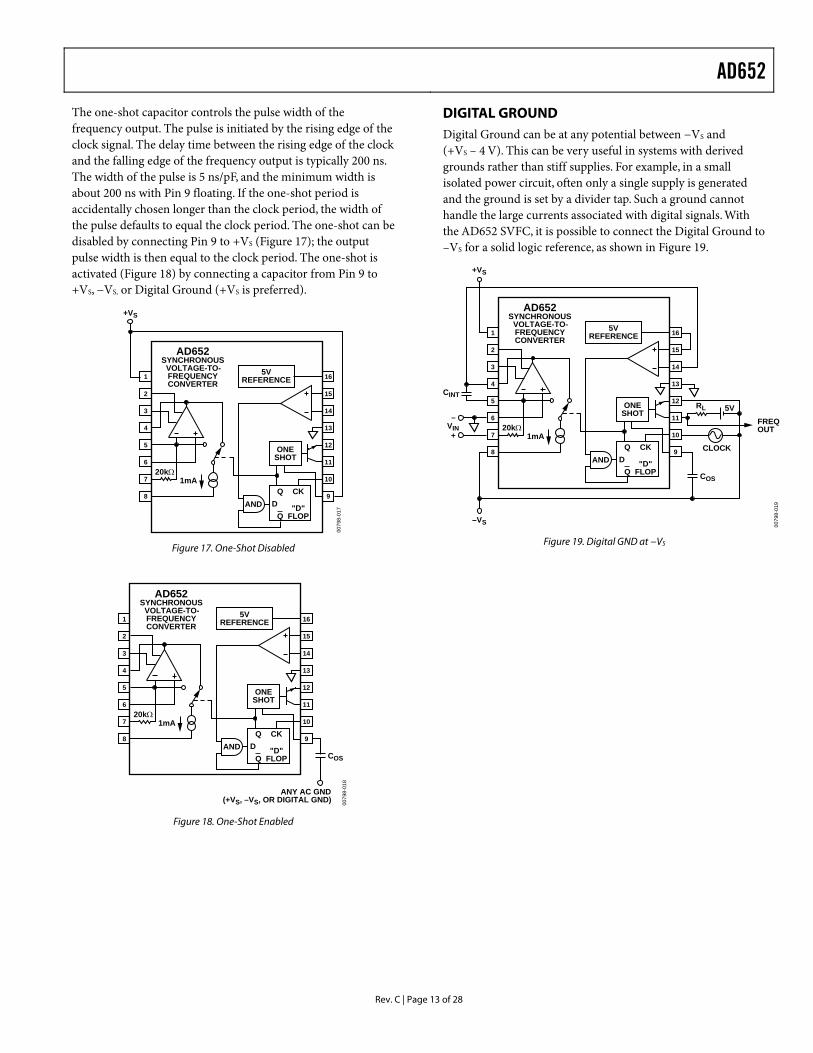
The one-shot capacitor controls the pulse width of the frequency output. The pulse is initiated by the rising edge of the clock signal. The delay time between the rising edge of the clock and the falling edge of the frequency output is typically 200 ns. The width of the pulse is 5 ns/pF, and the minimum width is about 200 ns with Pin 9 floating. If the one-shot period is accidentally chosen longer than the clock period, the width of the pulse defaults to equal the clock period. The one-shot can be disabled by connecting Pin 9 to +VS (Figure 17); the output pulse width is then equal to the clock period. The one-shot is activated (Figure 18) by connecting a capacitor from Pin 9 to +VS, −VS, or Digital Ground (+VS is preferred).
0079
8-01
7
1
2
3
4
5
6
7
8
16
15
14
13
12
11
10
9
ONESHOT
AND "D"FLOP
Q CKD
Q
1mA20kΩ
AD652SYNCHRONOUS
VOLTAGE-TO-FREQUENCYCONVERTER
5VREFERENCE
+VS
Figure 17. One-Shot Disabled
0079
8-01
8
1
2
3
4
5
6
7
8
16
15
14
13
12
11
10
9
ONESHOT
AND "D"FLOP
Q CKD
Q
1mA20kΩ
AD652SYNCHRONOUS
VOLTAGE-TO-FREQUENCYCONVERTER
5VREFERENCE
COS
ANY AC GND(+VS, –VS, OR DIGITAL GND)
Figure 18. One-Shot Enabled
DIGITAL GROUND Digital Ground can be at any potential between −VS and (+VS – 4 V). This can be very useful in systems with derived grounds rather than stiff supplies. For example, in a small isolated power circuit, often only a single supply is generated and the ground is set by a divider tap. Such a ground cannot handle the large currents associated with digital signals. With the AD652 SVFC, it is possible to connect the Digital Ground to –VS for a solid logic reference, as shown in Figure 19.
0079
8-01
9
+VS
1
2
3
4
–
+
5
6
7VIN
8
16
15
14
13
12
11
10
9
ONESHOT
AND "D"FLOP
Q CKD
Q
1mA20kΩ
AD652SYNCHRONOUS
VOLTAGE-TO-FREQUENCYCONVERTER
5VREFERENCE
RL 5V
CLOCK
FREQOUT
CINT
COS
–VS
Figure 19. Digital GND at −VS
AD652
Rev. C | Page 14 of 28
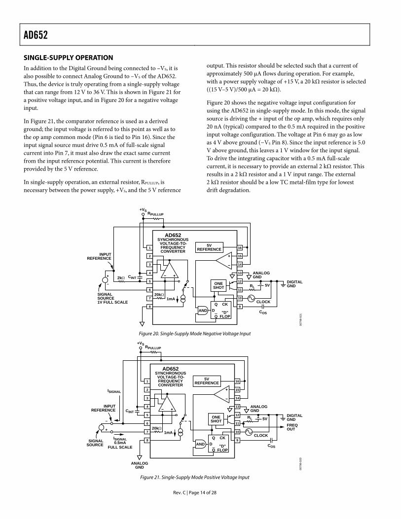
SINGLE-SUPPLY OPERATION In addition to the Digital Ground being connected to –VS, it is also possible to connect Analog Ground to –VS of the AD652. Thus, the device is truly operating from a single-supply voltage that can range from 12 V to 36 V. This is shown in Figure 21 for a positive voltage input, and in Figure 20 for a negative voltage input.
In Figure 21, the comparator reference is used as a derived ground; the input voltage is referred to this point as well as to the op amp common mode (Pin 6 is tied to Pin 16). Since the input signal source must drive 0.5 mA of full-scale signal current into Pin 7, it must also draw the exact same current from the input reference potential. This current is therefore provided by the 5 V reference.
In single-supply operation, an external resistor, RPULLUP, is necessary between the power supply, +VS, and the 5 V reference
output. This resistor should be selected such that a current of approximately 500 µA flows during operation. For example, with a power supply voltage of +15 V, a 20 kΩ resistor is selected ((15 V–5 V)/500 µA = 20 kΩ).
Figure 20 shows the negative voltage input configuration for using the AD652 in single-supply mode. In this mode, the signal source is driving the + input of the op amp, which requires only 20 nA (typical) compared to the 0.5 mA required in the positive input voltage configuration. The voltage at Pin 6 may go as low as 4 V above ground (−VS Pin 8). Since the input reference is 5.0 V above ground, this leaves a 1 V window for the input signal. To drive the integrating capacitor with a 0.5 mA full-scale current, it is necessary to provide an external 2 kΩ resistor. This results in a 2 kΩ resistor and a 1 V input range. The external 2 kΩ resistor should be a low TC metal-film type for lowest drift degradation.
0079
8-02
1
+VS
1
2
3
4
–
+5
6
7
8
16
15
14
13
12
11
10
9
ONESHOT
AND "D"FLOP
Q CKD
Q
1mA20kΩ
2kΩ
AD652SYNCHRONOUS
VOLTAGE-TO-FREQUENCYCONVERTER
5VREFERENCE
RL 5V
CLOCK
ANALOGGND
DIGITALGND
COS
CINT
SIGNALSOURCE1V FULL SCALE
INPUTREFERENCE
RPULLUP
Figure 20. Single-Supply Mode Negative Voltage Input
0079
8-02
0
+VS
1
2
3
4
–
+
5
6
7
8
16
15
14
13
12
11
10
9
ONESHOT
AND "D"FLOP
Q CKD
Q
1mA20kΩ
AD652SYNCHRONOUS
VOLTAGE-TO-FREQUENCYCONVERTER
5VREFERENCE
RL 5V
CLOCK
ANALOGGND
DIGITALGNDFREQOUT
COS
CINT
SIGNALSOURCE
ANALOGGND
ISIGNAL0.5mA
FULL SCALE
INPUTREFERENCE
RPULLUP
ISIGNAL
Figure 21. Single-Supply Mode Positive Voltage Input
AD652
Rev. C | Page 15 of 28
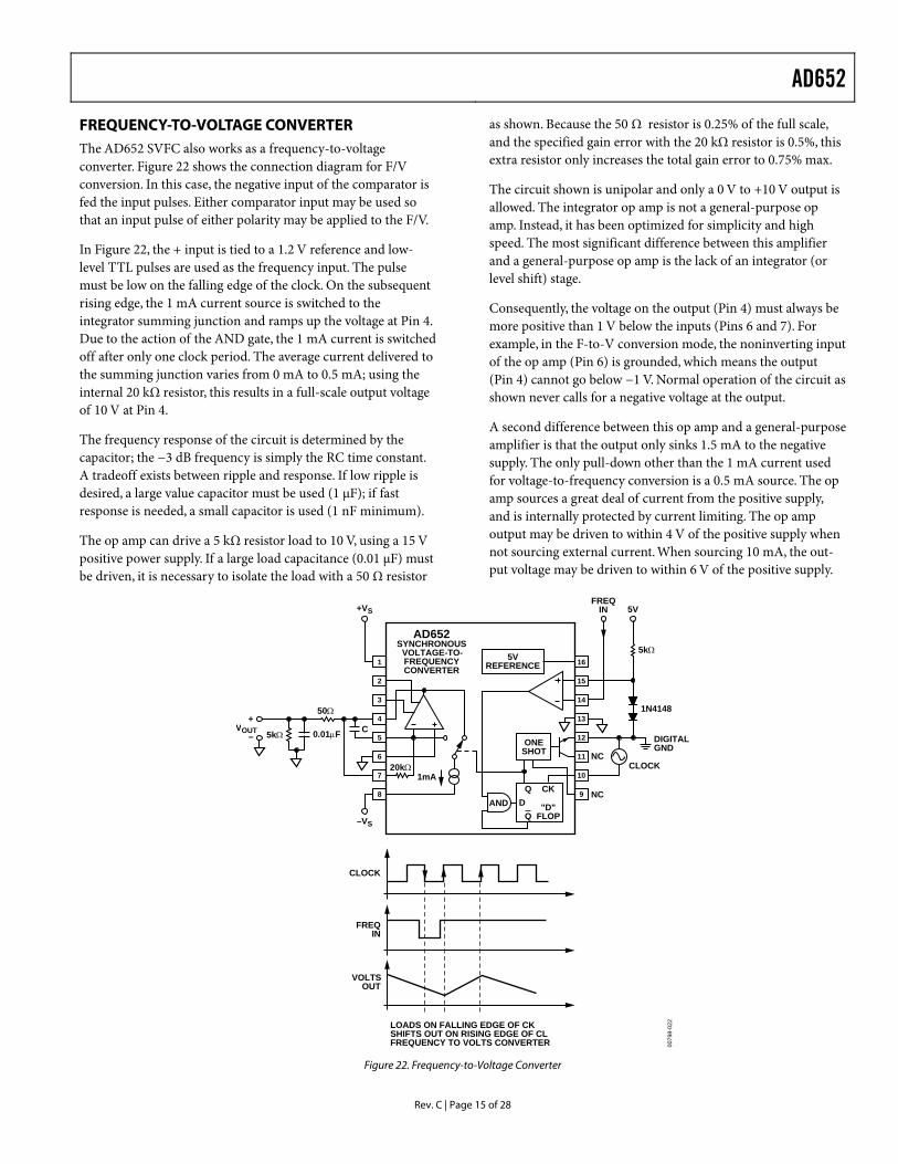
FREQUENCY-TO-VOLTAGE CONVERTER The AD652 SVFC also works as a frequency-to-voltage converter. Figure 22 shows the connection diagram for F/V conversion. In this case, the negative input of the comparator is fed the input pulses. Either comparator input may be used so that an input pulse of either polarity may be applied to the F/V.
In Figure 22, the + input is tied to a 1.2 V reference and low-level TTL pulses are used as the frequency input. The pulse must be low on the falling edge of the clock. On the subsequent rising edge, the 1 mA current source is switched to the integrator summing junction and ramps up the voltage at Pin 4. Due to the action of the AND gate, the 1 mA current is switched off after only one clock period. The average current delivered to the summing junction varies from 0 mA to 0.5 mA; using the internal 20 kΩ resistor, this results in a full-scale output voltage of 10 V at Pin 4.
The frequency response of the circuit is determined by the capacitor; the −3 dB frequency is simply the RC time constant. A tradeoff exists between ripple and response. If low ripple is desired, a large value capacitor must be used (1 µF); if fast response is needed, a small capacitor is used (1 nF minimum).
The op amp can drive a 5 kΩ resistor load to 10 V, using a 15 V positive power supply. If a large load capacitance (0.01 µF) must be driven, it is necessary to isolate the load with a 50 Ω resistor
as shown. Because the 50 Ω resistor is 0.25% of the full scale, and the specified gain error with the 20 kΩ resistor is 0.5%, this extra resistor only increases the total gain error to 0.75% max.
The circuit shown is unipolar and only a 0 V to +10 V output is allowed. The integrator op amp is not a general-purpose op amp. Instead, it has been optimized for simplicity and high speed. The most significant difference between this amplifier and a general-purpose op amp is the lack of an integrator (or level shift) stage.
Consequently, the voltage on the output (Pin 4) must always be more positive than 1 V below the inputs (Pins 6 and 7). For example, in the F-to-V conversion mode, the noninverting input of the op amp (Pin 6) is grounded, which means the output (Pin 4) cannot go below −1 V. Normal operation of the circuit as shown never calls for a negative voltage at the output.
A second difference between this op amp and a general-purpose amplifier is that the output only sinks 1.5 mA to the negative supply. The only pull-down other than the 1 mA current used for voltage-to-frequency conversion is a 0.5 mA source. The op amp sources a great deal of current from the positive supply, and is internally protected by current limiting. The op amp output may be driven to within 4 V of the positive supply when not sourcing external current. When sourcing 10 mA, the out-put voltage may be driven to within 6 V of the positive supply.
0079
8-02
2
CLOCK
FREQIN
VOLTSOUT
LOADS ON FALLING EDGE OF CKSHIFTS OUT ON RISING EDGE OF CLFREQUENCY TO VOLTS CONVERTER
+VS
–VS
1
2
3
4
5
6
7
8
16
15
14
13
12
11
10
9
ONESHOT
AND "D"FLOP
Q CKD
Q
1mA20kΩ
50Ω
0.01µF5kΩ
5kΩAD652
SYNCHRONOUSVOLTAGE-TO-FREQUENCYCONVERTER
5VREFERENCE
CLOCK
5VFREQ
IN
DIGITALGND
C
NC
NC
1N4148
–
+VOUT
Figure 22. Frequency-to-Voltage Converter
AD652
Rev. C | Page 16 of 28
DECOUPLING AND GROUNDING It is good engineering practice to use bypass capacitors on the supply-voltage pins, and to insert small valued resistors (10 Ω to 100 Ω) in the supply lines to provide a measure of decoupling between the various circuits in a system. Ceramic capacitors of 0.1 µF to 1.0 µF should be applied between the supply voltage pins and analog signal ground for proper bypassing on the AD652.
Additionally, a larger board-level decoupling capacitor of 1 µF to 10 µF should be located relatively close to the AD652 on each power supply line. Such precautions are imperative in high resolution data acquisition applications where one expects to exploit the full linearity and dynamic range of the AD652.
Separate digital and analog grounds are provided on the AD652. Only the emitter of the open-collector frequency output transistor and the clock input threshold are returned to the digital ground. Only the 5 V reference is connected to analog ground. The purpose of the two separate grounds is to allow isolation between the high precision analog signals and the digital section of the circuitry. Much noise can be tolerated on the digital ground without affecting the accuracy of the VFC. Such ground noise is inevitable when switching the large currents associated with the frequency output signal.
At high full-scale frequencies, it is necessary to use a pull-up resistor of about 500 Ω in order to get the rise time fast enough to provide well-defined output pulses. This means that from a 5 V logic supply, for example, the open collector output draws 10 mA. This much current being switched causes ringing on long ground runs due to the self-inductance of the wires. For instance, 20-gauge wire has an inductance of about 20 nH per inch; a current of 10 mA being switched in 50 ns at the end of 12 inches of 20-gauge wire produces a voltage spike of 50 mV. The separate digital ground of the AD652 easily handles these types of switching transients.
A problem remains from interference caused by radiation of electromagnetic energy from these fast transients. Typically, a voltage spike is produced by inductive switching transients; these spikes can capacitively couple into other sections of the circuit. Another problem is ringing of ground lines and power supply lines due to the distributed capacitance and inductance of the wires. Such ringing can also couple interference into sensitive analog circuits. The best solution to these problems is proper bypassing of the logic supply at the AD652 package. A 1 µF to 10 µF tantalum capacitor should be connected directly to the supply side of the pull-up resistor and to the digital ground, Pin 12. The pull-up resistor should be connected directly to the frequency output, Pin 11. The lead lengths on the bypass capacitor and the pull-up resistor should be as short as possible. The capacitor supplies (or absorbs) the current transients, and large ac signals flow in a physically small loop through the capacitor, pull-up resistor, and frequency output transistor. It is important that the loop be physically small for two reasons: first, there is less inductance if the wires are short, and second, the loop does not radiate RFI efficiently.
The digital ground (Pin 12) should be separately connected to the power supply ground. Note that the leads to the digital power supply are only carrying dc current. There may be a dc ground drop due to the difference in currents returned on the analog and digital grounds. This does not cause a problem; these features greatly ease power distribution and ground manage-ment in large systems. The proper technique for grounding requires separate digital and analog ground returns to the power supply. Also, the signal ground must be referred directly to the analog ground (Pin 6) at the package. More information on proper grounding and reduction of interference can be found in Noise Reduction Techniques in Electronic Systems, by H.W. Ort, (John Wiley, 1976).
AD652
Rev. C | Page 17 of 28
0079
8-02
3
+15V
1
2
3
4
5
6
7
200pF–15V
8
16
15
14
13
12
11
10
9
ONESHOT
AND "D"FLOP
Q CKD
Q
1mA20kΩ
AD652SYNCHRONOUS
VOLTAGE-TO-FREQUENCYCONVERTER
5VREFERENCE
+5V
0.02µF
–
+V2
0V–10V
fOUT
fC
+15V
1
2
3
4
5
6
7
–15V
8
16
15
14
13
12
11
10
9
ONESHOT
AND "D"FLOP
Q CKD
Q
1mA20kΩ
AD652SYNCHRONOUS
VOLTAGE-TO-FREQUENCYCONVERTER
5VREFERENCE
400pF
VOUT
2kΩ
+5V
1MHzCLOCKINPUT
4
3
OSC/DRIVERAB
74LS86
C
65
8
1
2
7
CT200pF
C1500pF
1kΩ
RPU2.87kΩ
RT1kΩ
R31kΩ
R22kΩ
R18.06kΩ
V10V–10V
+5V
AD654
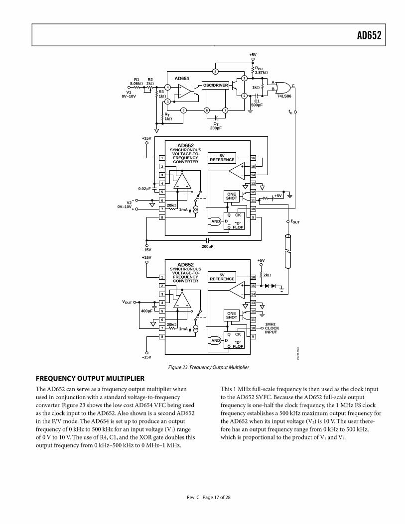
Figure 23. Frequency Output Multiplier
FREQUENCY OUTPUT MULTIPLIER The AD652 can serve as a frequency output multiplier when used in conjunction with a standard voltage-to-frequency converter. Figure 23 shows the low cost AD654 VFC being used as the clock input to the AD652. Also shown is a second AD652 in the F/V mode. The AD654 is set up to produce an output frequency of 0 kHz to 500 kHz for an input voltage (V1) range of 0 V to 10 V. The use of R4, C1, and the XOR gate doubles this output frequency from 0 kHz–500 kHz to 0 MHz–1 MHz.
This 1 MHz full-scale frequency is then used as the clock input to the AD652 SVFC. Because the AD652 full-scale output frequency is one-half the clock frequency, the 1 MHz FS clock frequency establishes a 500 kHz maximum output frequency for the AD652 when its input voltage (V2) is 10 V. The user there-fore has an output frequency range from 0 kHz to 500 kHz, which is proportional to the product of V1 and V2.
AD652
Rev. C | Page 18 of 28
This can be shown in equation form, where fC is the AD654 output frequency and fOUT is the AD652 output frequency:
V10MHz1
1C Vf =
⎟⎟⎟⎟
⎠
⎞
⎜⎜⎜⎜
⎝
⎛
=V10
2C
2OUT
f
Vf
( )( )⎟⎟⎠⎞
⎜⎜⎝
⎛=
V10V102MHz1
21OUT VVf
fOUT = V1 × V2 × 5 kHz/V2
The scope photo in Figure 24 shows V1 and V2 (top two traces) and the output of the F-V (bottom trace).
V1
V2
VOUT
0079
8-02
4
Figure 24. Multiplier Waveforms
SINGLE-LINE MULTIPLEXED DATA TRANSMISSION It is often necessary to measure several different signals and relay the information to some remote location using a mini-mum amount of cable. Multiple AD652 SVFC devices may be used with a multiphase clock to combine these measurements for serial transmission and demultiplexing. Figure 25 shows a block diagram of a single-line multiplexed data transmission
system with high noise immunity. Figure 26, Figure 27, and Figure 30 show the SVFC multiplexer, a representative means of data transmission, and an SVFC demultiplexer respectively.
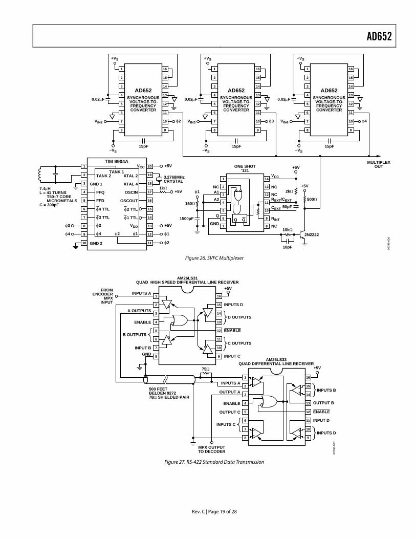
Multiplexer
Figure 30 shows the SVFC multiplexer. The clock inputs for the several SVFC channels are generated by a TIM9904A 4-phase clock driver, and the frequency outputs are combined by strapping all the frequency output pins together (a wire OR connection). The one-shot in the AD652 sets the pulse width of the frequency output pulses to be slightly shorter than one quarter of the clock period. Synchronization is achieved by applying one of the four available phases to a fixed TTL one-shot (’121) and combining the output with external transistor.
The width of this sync pulse is shorter than the width of the frequency output pulses to facilitate decoding the signal. The RC lag network on the input of the one-shot provides a slight delay between the rising edge of the clock and the sync pulse in order to match the 150 ns delay of the AD652 between the rising edge of the clock and the output pulse.
Transmitter
The multiplex signal can be transmitted in any manner suitable to the task at hand. A pulse transformer or an opto-isolator can provide galvanic isolation; extremely high voltage isolation or transmission through severe RF environments can be accomp-lished with a fiber optic link; telemetry can be achieved with a radio link. The circuit shown in Figure 27 uses an EIA RS-422 standard for digital data transmission over a balanced line. Figure 24 shows the waveforms of the four clock phases and the multiplex output signal. Note that the sync pulse is present every clock cycle, but the data pulses are no more frequent than every other clock cycle since the maximum output frequency from the SVFC is half the clock frequency. The clock frequency used in this circuit is 819.2 kHz, which provides more than 16 bits of resolution if 100 ms gate time is allowed for counting pulses of the decoded output frequencies.
0079
8-02
5
AD652
VIN1
AD652
VIN2
AD652
VIN3
ONESHOT
φ1 φ2 φ3 φ4
CLKGENERATOR SVFC MULTIPLEXER
(SEE FIGURE 26)
AD652
φ2
VOUT1
AD652
φ3
VOUT2
AD652
φ4
VOUT3
SVFCDEMUX
f1f2f3
SVFC DEMULTIPLEXER(SEE FIGURE 30)
DEMULTIPLEXER FREQUENCY TOVOLTAGE CONVERSION(SEE FIGURE 31)
TRANSMISSIONLINK
TRANSMISSIONLINK
(SEE FIGURE 27)
Figure 25. Single-Line Multiplexed Data Transmission Block Diagram
AD652
Rev. C | Page 19 of 28
0079
8-02
6
–VS
VIN2 φ2
+VS
0.02µF
1
2
3
4
5
6
7
8
16
15
14
13
12
11
10
9
AD652SYNCHRONOUS
VOLTAGE-TO-FREQUENCYCONVERTER
15pF–VS
VIN3 φ3
+VS
0.02µF
1
2
3
4
5
6
7
8
16
15
14
13
12
11
10
9
AD652SYNCHRONOUS
VOLTAGE-TO-FREQUENCYCONVERTER
15pF–VS
VIN4 φ4
+VS
0.02µF
1
2
3
4
5
6
7
8
16
15
14
13
12
11
10
9
AD652SYNCHRONOUS
VOLTAGE-TO-FREQUENCYCONVERTER
15pF
MULTIPLEXOUT
1 14
2 13
3 12
4 11
5 10
6 9
7 8
Q Q
ONE SHOT'121
φ1
150Ω
1500pFGND NC
RINT
CEXT
REXT/CEXTNC
NC
VCC
Q
A2
A1NC
18pF
10kΩ2N2222
500Ω
+5V2kΩ
50pF
+5V1 20
2 19
3 18
4 17
5 16
6 15
7 14
8 13
9 12
10 11
φ4
7.4µHL = 41 TURNS
T50–7 COREMICROMETALS
C = 300pF
φ3
φ1
+5V
+5V
3.2768MHzCRYSTAL
+5V
φ2
1kΩ
TANK 1
TIM 9904A
TANK 2 XTAL 2
XTAL 4
FFQ OSCIN
FFD OSCOUT
φ4 TTL φ2 TTL
φ3 TTL φ1 TTL
φ3 VDD
φ4 φ1φ2
GND 1
GND 2
VCC
Figure 26. SVFC Multiplexer
0079
8-02
7
INPUT BGND
75Ω
1
2
3
4
5
6
7
8
16
15
14
13
12
11
10
9
INPUTS AFROM
ENCODERMPX
INPUT
+5V
A OUTPUTS
ENABLE
B OUTPUTS
D OUTPUTS
C OUTPUTS
ENABLE
INPUTS D
INPUT C
500 FEETBELDEN 927278Ω SHIELDED PAIR
1
2
3
4
5
6
7
8
16
15
14
13
12
11
10
9
INPUTS A
+5V
MPX OUTPUTTO DECODER
AM26LS33QUAD DIFFERENTIAL LINE RECEIVER
AM26LS31QUAD HIGH SPEED DIFFERENTIAL LINE RECEIVER
OUTPUT A
OUTPUT C
ENABLE
INPUTS C
INPUTS B
INPUTS D
ENABLE
INPUT D
OUTPUT B
Figure 27. RS-422 Standard Data Transmission
AD652
Rev. C | Page 20 of 28
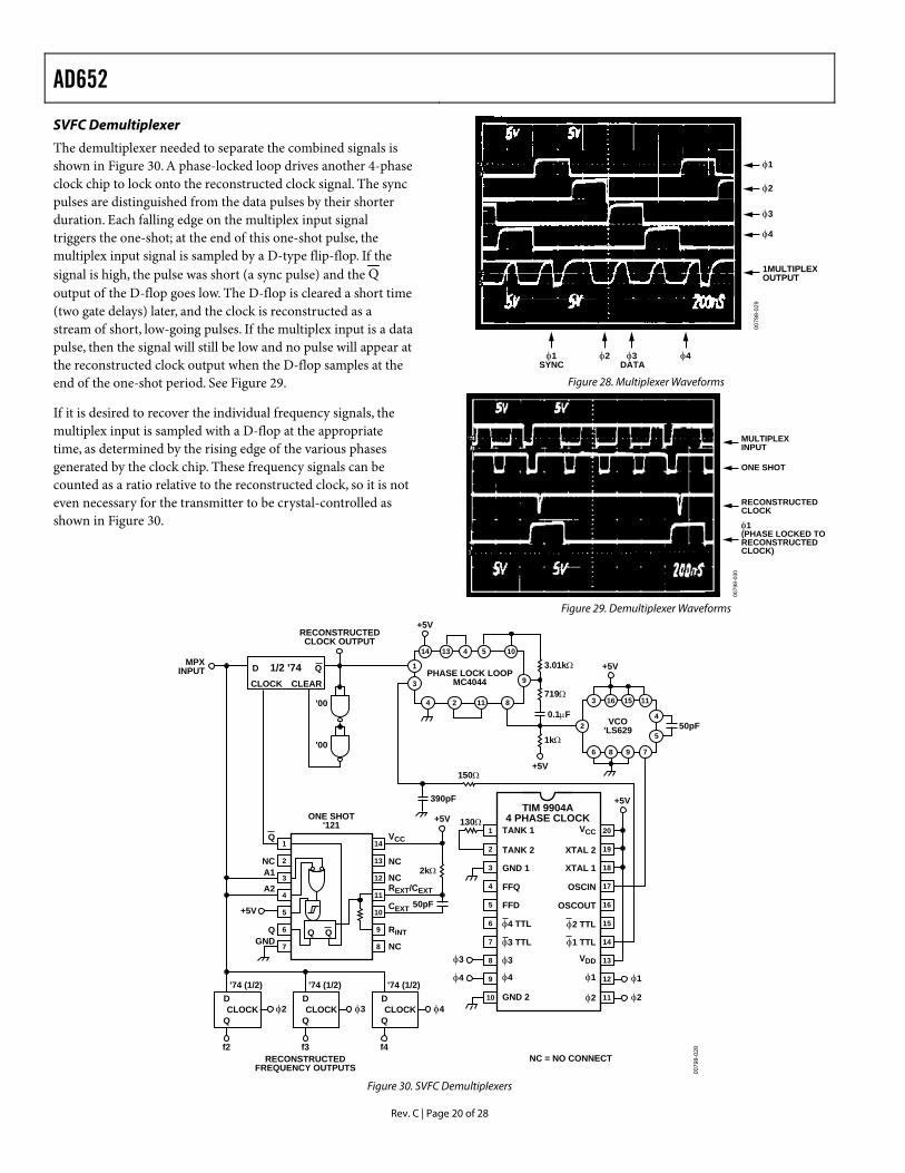
SVFC Demultiplexer
The demultiplexer needed to separate the combined signals is shown in Figure 30. A phase-locked loop drives another 4-phase clock chip to lock onto the reconstructed clock signal. The sync pulses are distinguished from the data pulses by their shorter duration. Each falling edge on the multiplex input signal triggers the one-shot; at the end of this one-shot pulse, the multiplex input signal is sampled by a D-type flip-flop. If the signal is high, the pulse was short (a sync pulse) and the Qoutput of the D-flop goes low. The D-flop is cleared a short time (two gate delays) later, and the clock is reconstructed as a stream of short, low-going pulses. If the multiplex input is a data pulse, then the signal will still be low and no pulse will appear at the reconstructed clock output when the D-flop samples at the end of the one-shot period. See Figure 29.
If it is desired to recover the individual frequency signals, the multiplex input is sampled with a D-flop at the appropriate time, as determined by the rising edge of the various phases generated by the clock chip. These frequency signals can be counted as a ratio relative to the reconstructed clock, so it is not even necessary for the transmitter to be crystal-controlled as shown in Figure 30.
0079
8-02
9
φ1
φ1SYNC
φ2 φ3DATA
φ4
φ2
φ3
φ4
1MULTIPLEXOUTPUT
Figure 28. Multiplexer Waveforms
0079
8-03
0
MULTIPLEXINPUT
ONE SHOT
RECONSTRUCTEDCLOCK
φ1(PHASE LOCKED TORECONSTRUCTEDCLOCK)
Figure 29. Demultiplexer Waveforms
0079
8-02
8
14 13 54 10
4 2 11 8
9
0.1µF
PHASE LOCK LOOPMC40443
1 3.01kΩ
719Ω
1kΩ
+5V
+5V
1 20
2 19
3 18
4 17
5 16
6 15
7 14
8 13
9 12
10 11
φ4
φ3
φ1
+5V
φ2
TANK 1
TIM 9904A4 PHASE CLOCK
TANK 2 XTAL 2
XTAL 1
FFQ OSCIN
FFD OSCOUT
φ3 VDD
φ4 φ1
φ2
GND 1
GND 2
VCC
φ1 TTL
φ2 TTL
φ3 TTL
φ4 TTL
130Ω
150Ω
3 16 15 11
6 8 9 7
24
5
+5V
50pFVCO'LS629
390pF
'00
'00
CLEAR
Q
CLOCK
D 1/2 '74
RECONSTRUCTEDCLOCK OUTPUT
MPXINPUT
1 14
2 13
3 12
4 11
5 10
6 9
7 8
Q Q
ONE SHOT'121
GND NC
RINT
CEXT
REXT/CEXTNC
NC
VCC
Q
+5V
A2
A1NC
2kΩ
50pF
+5V
Q
DCLOCK
Q
f2
φ2
'74 (1/2)DCLOCK
Q
f3RECONSTRUCTED
FREQUENCY OUTPUTS
φ3
'74 (1/2)DCLOCK
Q
f4
φ4
'74 (1/2)
NC = NO CONNECT
Figure 30. SVFC Demultiplexers
AD652
Rev. C | Page 21 of 28
0079
8-03
1–VS
φ2
+VS
1
2
3
4
5
6
7
8
16
15
14
13
12
11
10
9
AD652SYNCHRONOUS
VOLTAGE-TO-FREQUENCYCONVERTER
0.02µF
VOLTSOUTV2
+5V
4kΩ
MPX INPUT
–VS
φ3
+VS
1
2
3
4
5
6
7
8
16
15
14
13
12
11
10
9
AD652SYNCHRONOUS
VOLTAGE-TO-FREQUENCYCONVERTER
0.02µF
VOLTSOUTV3
–VS
φ4
+VS
1
2
3
4
5
6
7
8
16
15
14
13
12
11
10
9
AD652SYNCHRONOUS
VOLTAGE-TO-FREQUENCYCONVERTER
0.02µF
VOLTSOUTV4
1N4148
φ2, φ3, φ4 ARE PINS 15, 7, 6 OF TIM9904A FROM DEMUX FIGURE 30
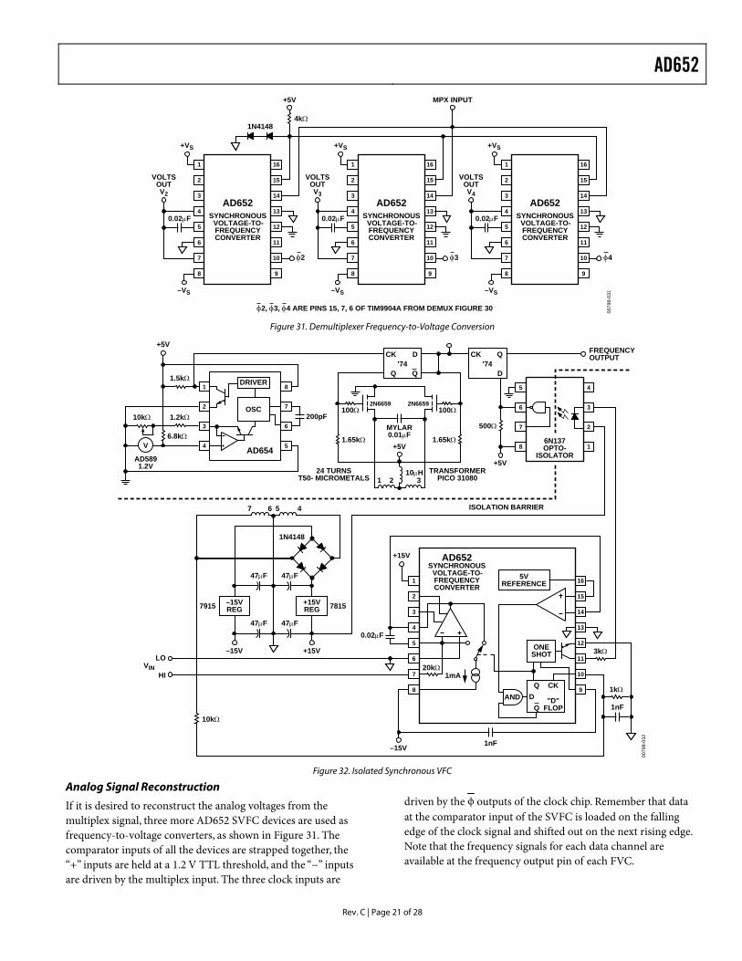
Figure 31. Demultiplexer Frequency-to-Voltage Conversion
0079
8-03
2
+5VTRANSFORMER
PICO 3108024 TURNS
T50- MICROMETALS
CK'74
Q
D
CK'74
Q
D
Q
500Ω
+15V
1
2
3
4
5
6
7
–15V
8
16
15
14
13
12
11
10
9
ONESHOT
AND "D"FLOP
Q CKD
Q
1mA20kΩ
AD652SYNCHRONOUS
VOLTAGE-TO-FREQUENCYCONVERTER
5VREFERENCE
0.02µF
1nF
LO
HIVIN
3kΩ
1kΩ
1nF
6N137OPTO-
ISOLATOR
5 4
6 3
7 2
8 1
ISOLATION BARRIER
FREQUENCYOUTPUT
2N6659 2N6659
MYLAR0.01µF
+5V
10µH
100Ω100Ω
1 2 3
1.65kΩ1.65kΩAD654
1 8
2 7
3 6
4 5
DRIVER
OSC200pF1.2kΩ
6.8kΩ
10kΩ
1.5kΩ
V
AD5891.2V
+5V
1N4148
4567
+15VREG 7815–15V
REG7915
47µF47µF
47µF47µF
+15V–15V
10kΩ
Figure 32. Isolated Synchronous VFC
Analog Signal Reconstruction
If it is desired to reconstruct the analog voltages from the multiplex signal, three more AD652 SVFC devices are used as frequency-to-voltage converters, as shown in Figure 31. The comparator inputs of all the devices are strapped together, the “+” inputs are held at a 1.2 V TTL threshold, and the “−” inputs are driven by the multiplex input. The three clock inputs are
driven by the ϕ outputs of the clock chip. Remember that data at the comparator input of the SVFC is loaded on the falling edge of the clock signal and shifted out on the next rising edge. Note that the frequency signals for each data channel are available at the frequency output pin of each FVC.
AD652
Rev. C | Page 22 of 28
ISOLATED FRONT END In some applications, it may be necessary to have complete galvanic isolation between the analog signals being measured and the digital portions of the circuit. The circuit shown in Figure 32 runs off a single 5 V power supply and provides a self-contained, completely isolated analog measurement system. The power for the AD652 SVFC is provided by a chopper and a transformer, and is regulated to 15 V.
Both the chopper frequency and the AD652 clock frequency are 125 kHz, with the clock signal being relayed to the SVFC through the transformer. The frequency output signal is relayed through an opto-isolator and latched into a D flop. The chopper frequency is generated from an AD654 VFC, and is frequency divided by two to develop differential drive for the chopper transistors, and to ensure an accurate 50% duty cycle. The pull-up resistors on the D flop outputs provide a well-defined high level voltage to the choppers to equalize the drive in each direction. The 10 µH inductor in the 5 V lead of the transformer primary is necessary to equalize any residual imbalance in the drive on each half cycle, and thus prevent saturation of the core. The capacitor across the primary resonates the system so that under light loading conditions on the secondary, the wave shape is sinusoidal and the clock frequency is relayed to the SVFC. To adjust the chopper frequency, disconnect any load on the secondary and tune the AD654 for a minimum in the supply current drawn from the 5 V supply.
A-TO-D CONVERSION In performing an A-to-D conversion, the output pulses of a VFC are counted for a fixed-gate interval. To achieve maximum performance with the AD652, the fixed-gate interval should be generated using a multiple of the SVFC clock input. Counting in this manner eliminates any errors due to the clock (whether it be jitter, drift with time or temperature, and so on) since it is the ratio of the clock and output frequencies that is being measured.
The resolution of the A-to-D conversion measurement is determined by the clock frequency and the gate time. If, for instance, a resolution of 12 bits is desired and the clock frequency is 1 MHz (resulting in an AD652 FS frequency of 500 kHz) the gate time is:
( )
ms192.8sec101
819240962MHz1
21
6
111–
=×
=
⎟⎟⎠
⎞⎜⎜⎝
⎛=⎟⎟
⎠
⎞⎜⎜⎝
⎛=⎟⎟
⎠
⎞⎜⎜⎝
⎛−−
NFreqClock
NFreqFS
Where N is the total number of codes for a given resolution.
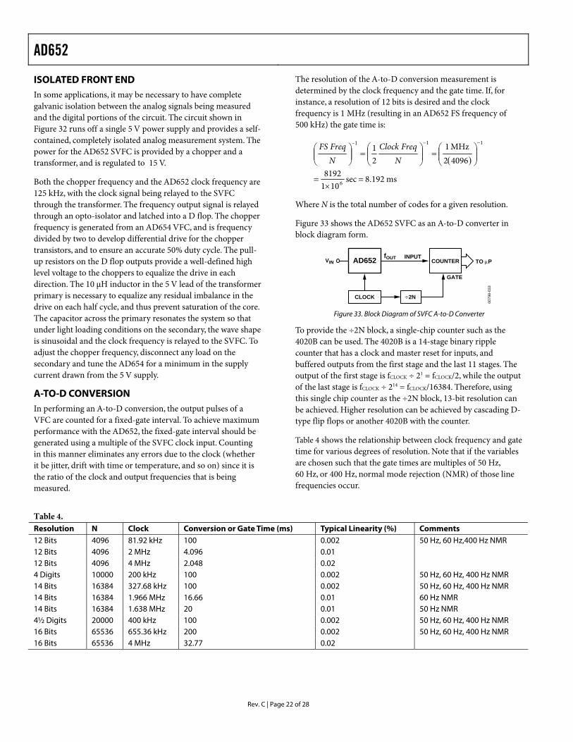
Figure 33 shows the AD652 SVFC as an A-to-D converter in block diagram form.
0079
8-03
3
VIN AD652 COUNTER TO µPINPUT
GATE
fOUT
CLOCK ÷2N
Figure 33. Block Diagram of SVFC A-to-D Converter
To provide the ÷2N block, a single-chip counter such as the 4020B can be used. The 4020B is a 14-stage binary ripple counter that has a clock and master reset for inputs, and buffered outputs from the first stage and the last 11 stages. The output of the first stage is fCLOCK ÷ 21 = fCLOCK/2, while the output of the last stage is fCLOCK ÷ 214 = fCLOCK/16384. Therefore, using this single chip counter as the ÷2N block, 13-bit resolution can be achieved. Higher resolution can be achieved by cascading D-type flip flops or another 4020B with the counter.
Table 4 shows the relationship between clock frequency and gate time for various degrees of resolution. Note that if the variables are chosen such that the gate times are multiples of 50 Hz, 60 Hz, or 400 Hz, normal mode rejection (NMR) of those line frequencies occur.
Table 4. Resolution N Clock Conversion or Gate Time (ms) Typical Linearity (%) Comments 12 Bits 4096 81.92 kHz 100 0.002 50 Hz, 60 Hz,400 Hz NMR 12 Bits 4096 2 MHz 4.096 0.01 12 Bits 4096 4 MHz 2.048 0.02 4 Digits 10000 200 kHz 100 0.002 50 Hz, 60 Hz, 400 Hz NMR 14 Bits 16384 327.68 kHz 100 0.002 50 Hz, 60 Hz, 400 Hz NMR 14 Bits 16384 1.966 MHz 16.66 0.01 60 Hz NMR 14 Bits 16384 1.638 MHz 20 0.01 50 Hz NMR 4½ Digits 20000 400 kHz 100 0.002 50 Hz, 60 Hz, 400 Hz NMR 16 Bits 65536 655.36 kHz 200 0.002 50 Hz, 60 Hz, 400 Hz NMR 16 Bits 65536 4 MHz 32.77 0.02
AD652
Rev. C | Page 23 of 28
DELTA MODULATOR The circuit of Figure 34 shows the AD652 configured as a delta modulator. A reference voltage is applied to the input of the integrator (Pin 7), which sets the steady state output frequency at one-half of the AD652 full-scale frequency (1/4 of the clock frequency). As a 0 V to 10 V input signal is applied to the comparator (Pin 15), the output of the integrator attempts to track this signal. For an input in an idling condition (dc), the output frequency is one-half full scale. For positive-going signals, the output frequency is between one-half full scale and full scale; for negative-going signals, the output frequency is between zero and one-half full scale. The output frequency corresponds to the slope of the comparator input signal.
0079
8-03
4
1
2
3
4
5
6
7
8
16
15
14
13
12
11
10
9
ONESHOT
AND "D"FLOP
Q CKD
Q
1mA20kΩ
AD652SYNCHRONOUS
VOLTAGE-TO-FREQUENCYCONVERTER
5VREFERENCE+15V
360pF
0.0047µF
–15V
CLOCK
VIN (0V TO 10V)
FOUT
+5V
0.01µF
1kΩ
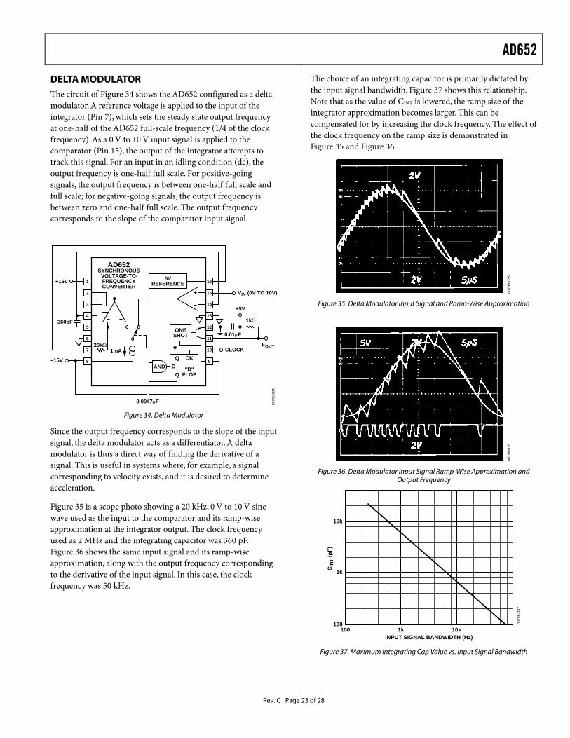
Figure 34. Delta Modulator
Since the output frequency corresponds to the slope of the input signal, the delta modulator acts as a differentiator. A delta modulator is thus a direct way of finding the derivative of a signal. This is useful in systems where, for example, a signal corresponding to velocity exists, and it is desired to determine acceleration.
Figure 35 is a scope photo showing a 20 kHz, 0 V to 10 V sine wave used as the input to the comparator and its ramp-wise approximation at the integrator output. The clock frequency used as 2 MHz and the integrating capacitor was 360 pF. Figure 36 shows the same input signal and its ramp-wise approximation, along with the output frequency corresponding to the derivative of the input signal. In this case, the clock frequency was 50 kHz.
The choice of an integrating capacitor is primarily dictated by the input signal bandwidth. Figure 37 shows this relationship. Note that as the value of CINT is lowered, the ramp size of the integrator approximation becomes larger. This can be compensated for by increasing the clock frequency. The effect of the clock frequency on the ramp size is demonstrated in Figure 35 and Figure 36.
0079
8-03
5
Figure 35. Delta Modulator Input Signal and Ramp-Wise Approximation
0079
8-03
6
Figure 36. Delta Modulator Input Signal Ramp-Wise Approximation and Output Frequency
100
1k
10k
100 1k 10k
0079
8-03
7
INPUT SIGNAL BANDWIDTH (Hz)
CIN
T (p
F)
Figure 37. Maximum Integrating Cap Value vs. Input Signal Bandwidth
AD652
Rev. C | Page 24 of 28
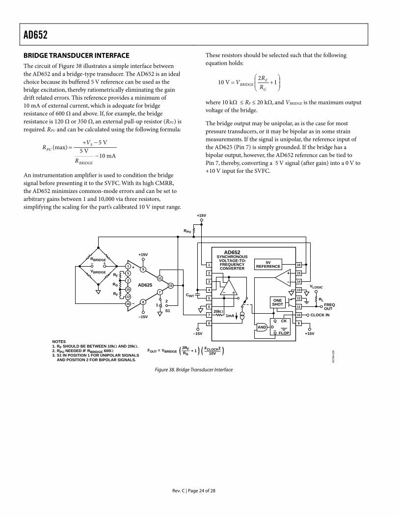
BRIDGE TRANSDUCER INTERFACE The circuit of Figure 38 illustrates a simple interface between the AD652 and a bridge-type transducer. The AD652 is an ideal choice because its buffered 5 V reference can be used as the bridge excitation, thereby ratiometrically eliminating the gain drift related errors. This reference provides a minimum of 10 mA of external current, which is adequate for bridge resistance of 600 Ω and above. If, for example, the bridge resistance is 120 Ω or 350 Ω, an external pull-up resistor (RPU) is required. RPU and can be calculated using the following formula:
mA10V5
V5(max)
−
−+=
BRIDGE
SPU
R
VR
An instrumentation amplifier is used to condition the bridge signal before presenting it to the SVFC. With its high CMRR, the AD652 minimizes common-mode errors and can be set to arbitrary gains between 1 and 10,000 via three resistors, simplifying the scaling for the part’s calibrated 10 V input range.
These resistors should be selected such that the following equation holds:
⎟⎟⎠
⎞⎜⎜⎝
⎛+= 1
2V10
G
FBRIDGE R
RV
where 10 kΩ ≤ RF ≤ 20 kΩ, and VBRIDGE is the maximum output voltage of the bridge.
The bridge output may be unipolar, as is the case for most pressure transducers, or it may be bipolar as in some strain measurements. If the signal is unipolar, the reference input of the AD625 (Pin 7) is simply grounded. If the bridge has a bipolar output, however, the AD652 reference can be tied to Pin 7, thereby, converting a 5 V signal (after gain) into a 0 V to +10 V input for the SVFC.
0079
8-03
8
1
2
3
4
5
6
7
8
16
15
14
13
12
11
10
9
ONESHOT
AND "D"FLOP
Q CKD
Q
1mA20kΩ
AD652SYNCHRONOUS
VOLTAGE-TO-FREQUENCYCONVERTER
5VREFERENCE
9
8
11
7
10
1
5
2
15
12
16
AD625
RBRIDGE
VBRIDGE
+–
RF
RG
RF
+15V
–15V
12
S1
+15V
CLOCK IN
FREQOUT
+15V
VLOGIC
RL
RPU
–15V
CINT
NOTES1. RF SHOULD BE BETWEEN 10kΩ AND 20kΩ.2. RPU NEEDED IF RBRIDGE 600Ω3. S1 IN POSITION 1 FOR UNIPOLAR SIGNALS
AND POSITION 2 FOR BIPOLAR SIGNALS.
FOUT = VBRIDGEFCLOCK2
10V + 12RFRG
Figure 38. Bridge Transducer Interface
AD652
Rev. C | Page 25 of 28
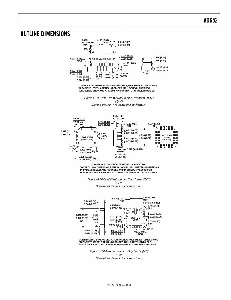
OUTLINE DIMENSIONS
16
1 8
9
0.310 (7.87)0.220 (5.59)
PIN 1
0.005(0.13)
MIN
0.098 (2.49)MAX
15°0°
0.320 (8.13)0.290 (7.37)
0.015 (0.38)0.008 (0.20)
SEATINGPLANE
0.200 (5.08)MAX
0.840 (21.34) MAX
0.150 (3.81)MIN
0.200 (5.08)0.125 (3.18)
0.023 (0.58)0.014 (0.36)
0.100(2.54)BSC
0.070 (1.78)0.030 (0.76)
0.060 (1.52)0.015 (0.38)
CONTROLLING DIMENSIONS ARE IN INCHES; MILLIMETER DIMENSIONS(IN PARENTHESES) ARE ROUNDED-OFF INCH EQUIVALENTS FORREFERENCE ONLY AND ARE NOT APPROPRIATE FOR USE IN DESIGN
Figure 39. 16-Lead Ceramic Dual In-Line Package [CERDIP] (Q-16)
Dimensions shown in inches and (millimeters)
0.020 (0.50)R
BOTTOMVIEW
(PINS UP)
0.025 (0.64) MIN
0.021 (0.53)0.013 (0.33)
0.330 (8.38)0.290 (7.37)0.032 (0.81)
0.026 (0.66)
0.056 (1.42)0.042 (1.07) 0.20 (0.51)
MIN
0.120 (3.04)0.090 (2.29)
34
1918
89
1413
TOP VIEW(PINS DOWN)
0.395 (10.02)0.385 (9.78) SQ
0.356 (9.04)0.350 (8.89)SQ
0.048 (1.21)0.042 (1.07)
0.048 (1.21)0.042 (1.07)
0.020(0.50)
R
0.050(1.27)BSC
0.180 (4.57)0.165 (4.19)
COMPLIANT TO JEDEC STANDARDS MO-047AACONTROLLING DIMENSIONS ARE IN INCHES; MILLIMETER DIMENSIONS(IN PARENTHESES) ARE ROUNDED-OFF INCH EQUIVALENTS FORREFERENCE ONLY AND ARE NOT APPROPRIATE FOR USE IN DESIGN
Figure 40. 20-Lead Plastic Leaded Chip Carrier [PLCC] (P-20A)
Dimensions shown in inches and (mm)
1
20 4
98
13
19
14
318
BOTTOMVIEW
0.028 (0.71)0.022 (0.56)
45° TYP
0.015 (0.38)MIN
0.055 (1.40)0.045 (1.14)
0.050 (1.27)BSC0.075 (1.91)
REF
0.011 (0.28)0.007 (0.18)
R TYP
0.095 (2.41)0.075 (1.90)
0.100 (2.54) REF
0.200 (5.08)REF
0.150 (3.81)BSC
0.075 (1.91)REF
0.358 (9.09)0.342 (8.69)
SQ
0.358(9.09)MAX
SQ
0.100 (2.54)0.064 (1.63)
0.088 (2.24)0.054 (1.37)
CONTROLLING DIMENSIONS ARE IN INCHES; MILLIMETER DIMENSIONS(IN PARENTHESES) ARE ROUNDED-OFF INCH EQUIVALENTS FORREFERENCE ONLY AND ARE NOT APPROPRIATE FOR USE IN DESIGN
Figure 41. 20-Terminal Leadless Chip Carrier [LCC] (E-20A)
Dimensions shown in inches and (mm)
AD652
Rev. C | Page 26 of 28
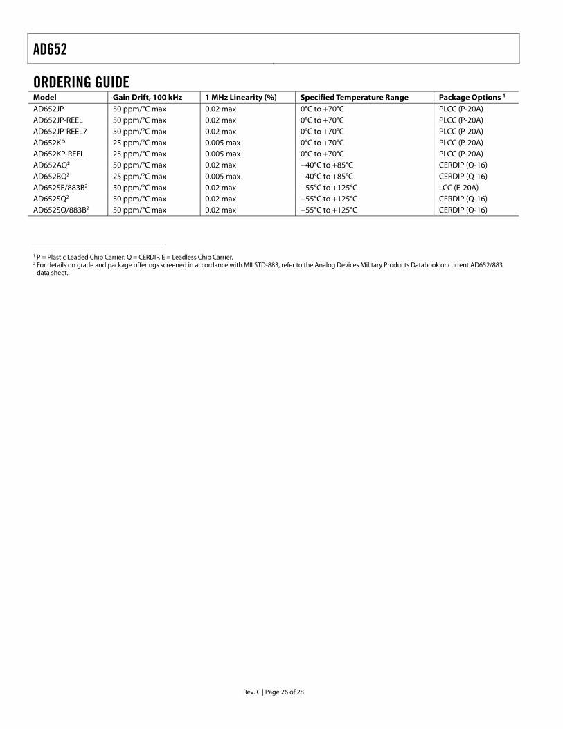
ORDERING GUIDE Model Gain Drift, 100 kHz 1 MHz Linearity (%) Specified Temperature Range Package Options 1
AD652JP 50 ppm/°C max 0.02 max 0°C to +70°C PLCC (P-20A) AD652JP-REEL 50 ppm/°C max 0.02 max 0°C to +70°C PLCC (P-20A) AD652JP-REEL7 50 ppm/°C max 0.02 max 0°C to +70°C PLCC (P-20A) AD652KP 25 ppm/°C max 0.005 max 0°C to +70°C PLCC (P-20A) AD652KP-REEL 25 ppm/°C max 0.005 max 0°C to +70°C PLCC (P-20A) AD652AQ2 50 ppm/°C max 0.02 max −40°C to +85°C CERDIP (Q-16) AD652BQ2 25 ppm/°C max 0.005 max −40°C to +85°C CERDIP (Q-16) AD652SE/883B2 50 ppm/°C max 0.02 max −55°C to +125°C LCC (E-20A) AD652SQ2 50 ppm/°C max 0.02 max −55°C to +125°C CERDIP (Q-16) AD652SQ/883B2 50 ppm/°C max 0.02 max −55°C to +125°C CERDIP (Q-16)
1 P = Plastic Leaded Chip Carrier; Q = CERDIP, E = Leadless Chip Carrier. 2 For details on grade and package offerings screened in accordance with MILSTD-883, refer to the Analog Devices Military Products Databook or current AD652/883
data sheet.

AD652
Rev. C | Page 27 of 28
NOTES

AD652
Rev. C | Page 28 of 28
NOTES
© 2004 Analog Devices, Inc. All rights reserved. Trademarks and registered trademarks are the property of their respective owners. C00798–0–5/04(C)