monolithic 3d inc., patents pending monolithic 3d ics october 2012 1 monolithic 3d inc., patents...
TRANSCRIPT
MonolithIC 3D Inc. , Patents Pending
MonolithIC 3D ICs
October 2012
1MonolithIC 3D Inc. , Patents Pending
MonolithIC 3D Inc. Patents Pending 2
Chapter 1Monolithic 3D
3D ICs at a glance
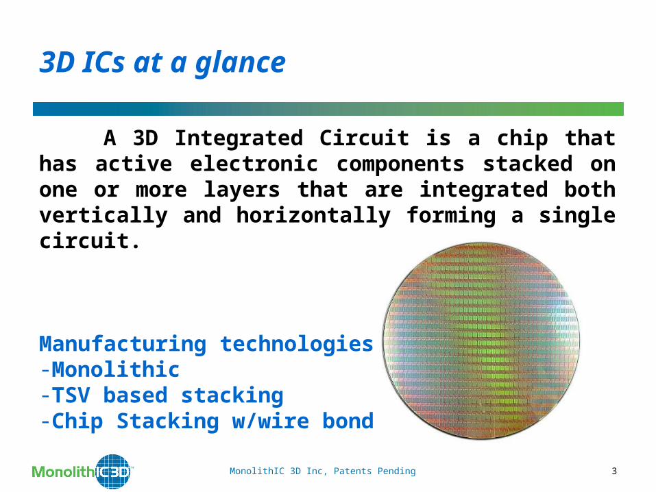
A 3D Integrated Circuit is a chip that has active electronic components stacked on one or more layers that are integrated both vertically and horizontally forming a single circuit.
Manufacturing technologies:-Monolithic-TSV based stacking-Chip Stacking w/wire bonding
MonolithIC 3D Inc, Patents Pending 3
MonolithIC 3D
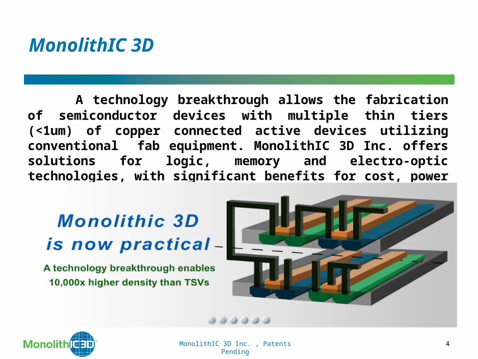
A technology breakthrough allows the fabrication of semiconductor devices with multiple thin tiers (<1um) of copper connected active devices utilizing conventional fab equipment. MonolithIC 3D Inc. offers solutions for logic, memory and electro-optic technologies, with significant benefits for cost, power and operating speed.
MonolithIC 3D Inc. , Patents Pending 4
Comparison of Through-Silicon Via (TSV) 3D Technology and Monolithic 3D Technology
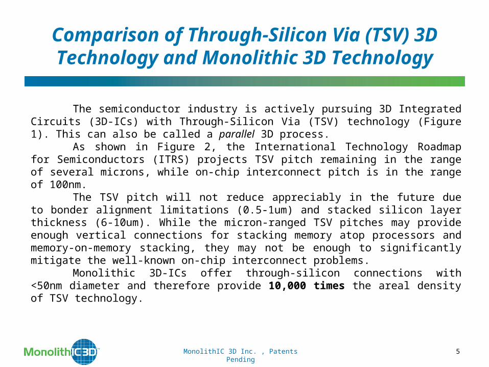
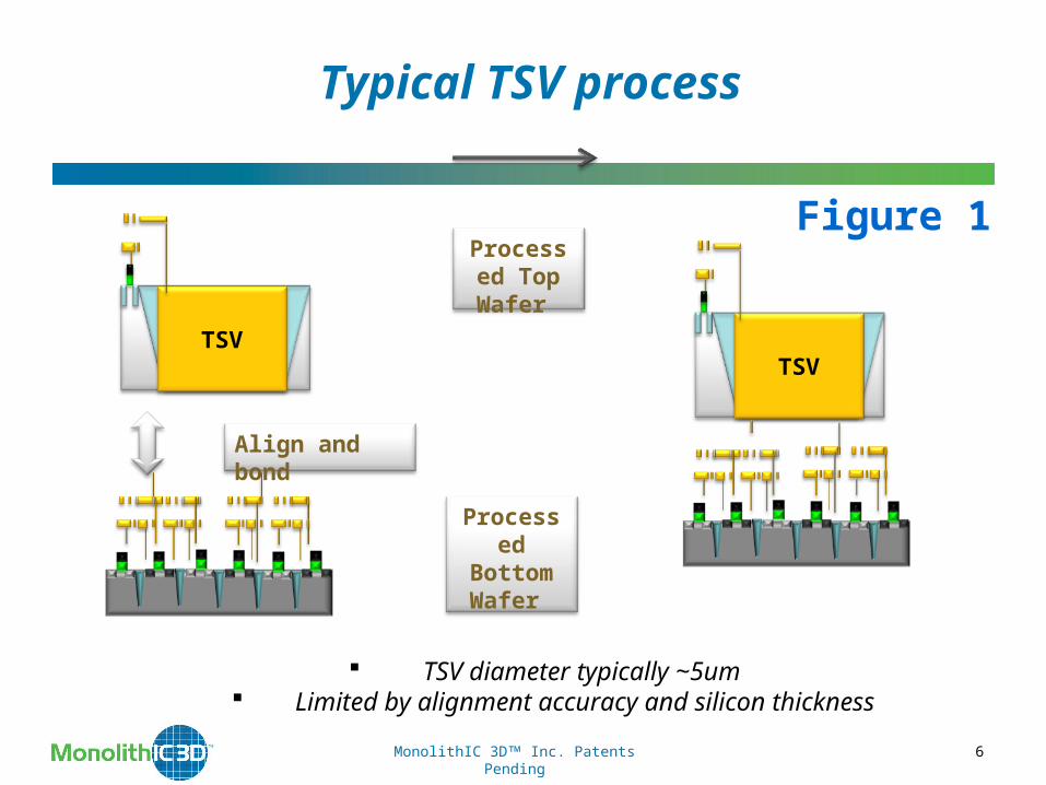
The semiconductor industry is actively pursuing 3D Integrated Circuits (3D-ICs) with Through-Silicon Via (TSV) technology (Figure 1). This can also be called a parallel 3D process.
As shown in Figure 2, the International Technology Roadmap for Semiconductors (ITRS) projects TSV pitch remaining in the range of several microns, while on-chip interconnect pitch is in the range of 100nm.
The TSV pitch will not reduce appreciably in the future due to bonder alignment limitations (0.5-1um) and stacked silicon layer thickness (6-10um).
While the micron-ranged TSV pitches may provide enough vertical connections for stacking memory atop processors and memory-on-memory stacking, they may not be enough to significantly mitigate the well-known on-chip interconnect problems.
Monolithic 3D-ICs offer through-silicon connections with <50nm diameter and therefore provide 10,000 times the areal density of TSV technology.
MonolithIC 3D Inc. , Patents Pending 5
MonolithIC 3D Inc. Patents Pending 6
Typical TSV process
TSV diameter typically ~5um Limited by alignment accuracy and silicon thickness
Processed Top Wafer
Processed Bottom Wafer
Align and bond
TSVTSV
Figure 1
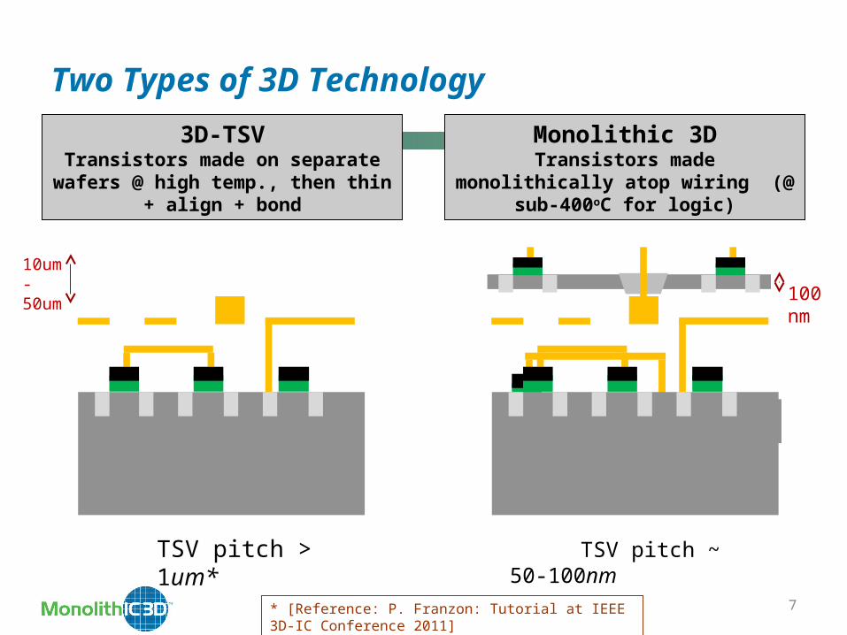
Two Types of 3D Technology
7
3D-TSVTransistors made on separate wafers @ high temp., then thin + align + bond
TSV pitch > 1um*
Monolithic 3DTransistors made monolithically atop
wiring (@ sub-400oC for logic)
TSV pitch ~ 50-100nm
10um-50um 100
nm
* [Reference: P. Franzon: Tutorial at IEEE 3D-IC Conference 2011]

Figure 2ITRS Roadmap compared to monolithic 3D
MonolithIC 3D Inc. , Patents Pending 8
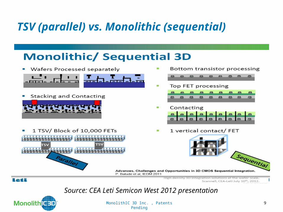
TSV (parallel) vs. Monolithic (sequential)
MonolithIC 3D Inc. , Patents Pending 9
Source: CEA Leti Semicon West 2012 presentation
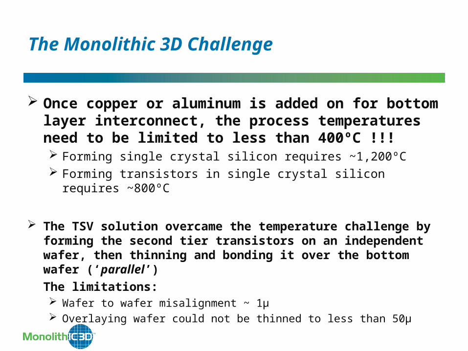
The Monolithic 3D Challenge
Once copper or aluminum is added on for bottom layer interconnect, the process temperatures need to be limited to less than 400ºC !!! Forming single crystal silicon requires ~1,200ºC Forming transistors in single crystal silicon requires ~800ºC
The TSV solution overcame the temperature challenge by forming the second tier transistors on an independent wafer, then thinning and bonding it over the bottom wafer (‘parallel’)
The limitations: Wafer to wafer misalignment ~ 1µ Overlaying wafer could not be thinned to less than 50µ
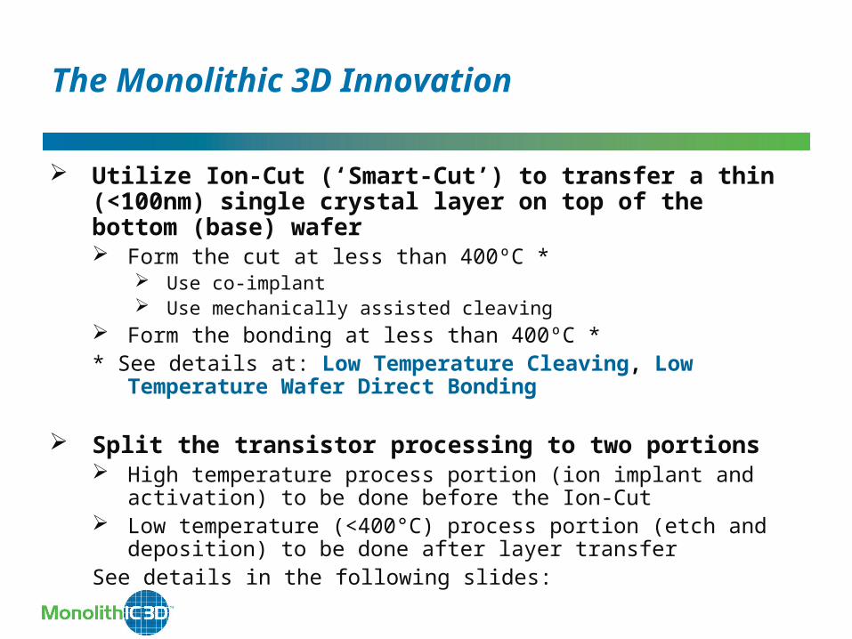
The Monolithic 3D Innovation
Utilize Ion-Cut (‘Smart-Cut’) to transfer a thin (<100nm) single crystal layer on top of the bottom (base) wafer Form the cut at less than 400ºC *
Use co-implant Use mechanically assisted cleaving
Form the bonding at less than 400ºC ** See details at: Low Temperature Cleaving, Low Temperature Wafer
Direct Bonding
Split the transistor processing to two portions High temperature process portion (ion implant and activation) to be
done before the Ion-Cut Low temperature (<400°C) process portion (etch and deposition) to be
done after layer transferSee details in the following slides:
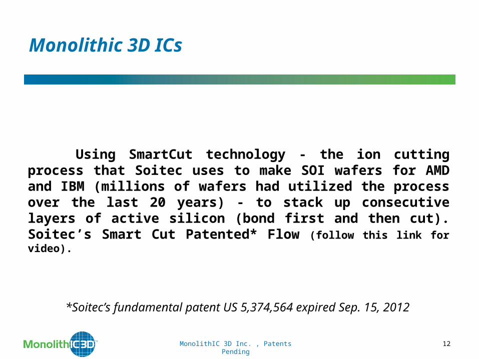
Monolithic 3D ICs
Using SmartCut technology - the ion cutting process that Soitec uses to make SOI wafers for AMD and IBM (millions of wafers had utilized the process over the last 20 years) - to stack up consecutive layers of active silicon (bond first and then cut). Soitec’s Smart Cut Patented* Flow (follow this link for video).
MonolithIC 3D Inc. , Patents Pending 12
*Soitec’s fundamental patent US 5,374,564 expired Sep. 15, 2012
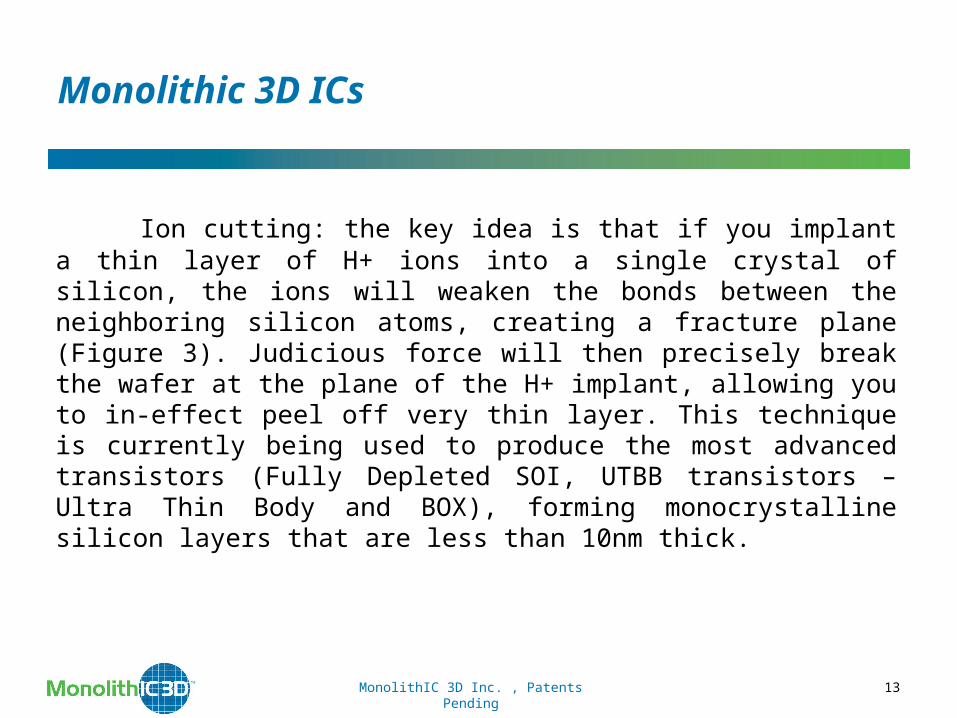
Monolithic 3D ICs
Ion cutting: the key idea is that if you implant a thin layer of H+ ions into a single crystal of silicon, the ions will weaken the bonds between the neighboring silicon atoms, creating a fracture plane (Figure 3). Judicious force will then precisely break the wafer at the plane of the H+ implant, allowing you to in-effect peel off very thin layer. This technique is currently being used to produce the most advanced transistors (Fully Depleted SOI, UTBB transistors – Ultra Thin Body and BOX), forming monocrystalline silicon layers that are less than 10nm thick.
MonolithIC 3D Inc. , Patents Pending 13
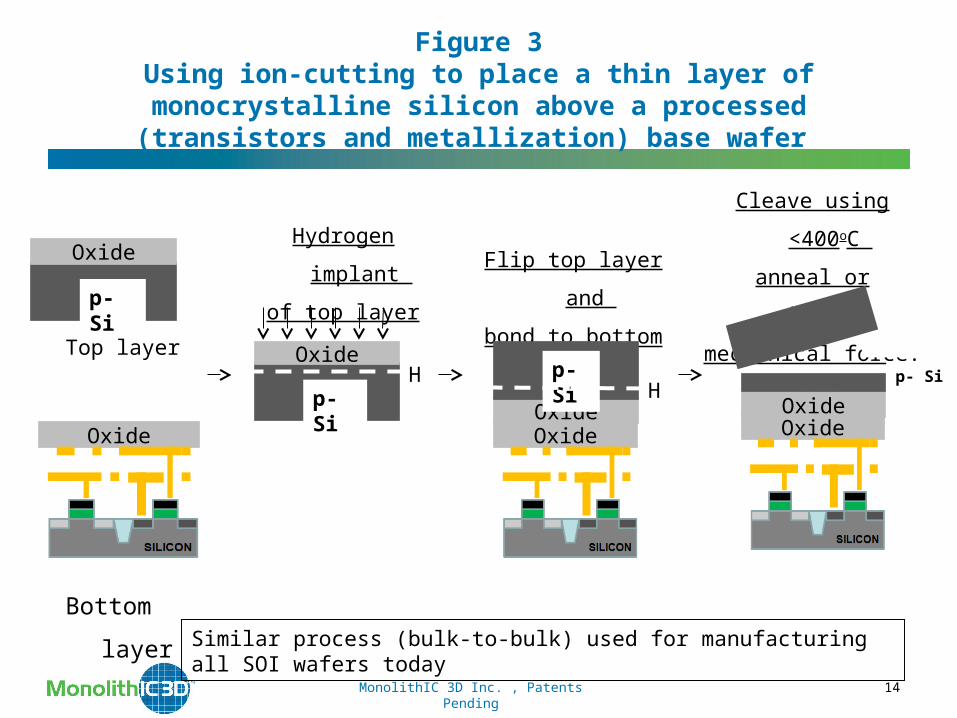
Figure 3Using ion-cutting to place a thin layer of monocrystalline silicon
above a processed (transistors and metallization) base wafer
MonolithIC 3D Inc. , Patents Pending 14
p- Si
Oxide
p- Si
OxideH
Top layer
Bottom layer
Oxide
Hydrogen implant
of top layerFlip top layer and
bond to bottom layer
Oxide
p- Si
Oxide
H
Cleave using <400oC
anneal or sideways
mechanical force.
CMP.
OxideOxide
Similar process (bulk-to-bulk) used for manufacturing all SOI wafers today
p- Si
MonolithIC 3D Inc. Patents Pending 15
Chapter 2Monolithic 3D RCAT
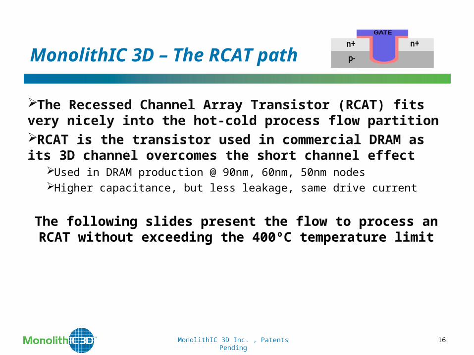
MonolithIC 3D – The RCAT path
The Recessed Channel Array Transistor (RCAT) fits very nicely into the hot-cold process flow partitionRCAT is the transistor used in commercial DRAM as its 3D channel overcomes the short channel effect
Used in DRAM production @ 90nm, 60nm, 50nm nodesHigher capacitance, but less leakage, same drive current
The following slides present the flow to process an RCAT without exceeding the 400ºC temperature limit
MonolithIC 3D Inc. , Patents Pending 16
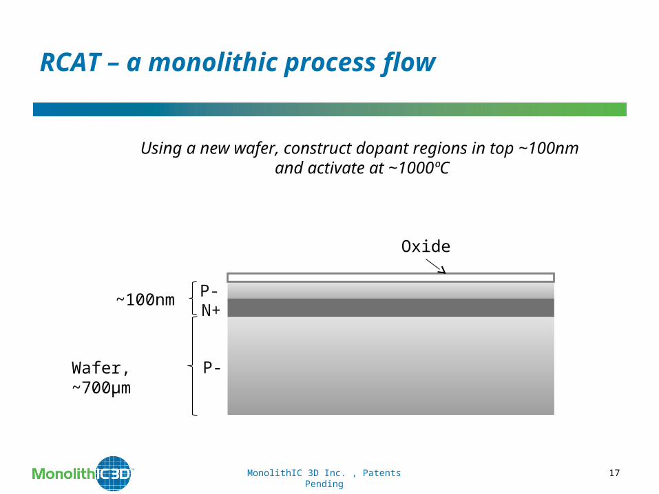
RCAT – a monolithic process flow
MonolithIC 3D Inc. , Patents Pending 17
Wafer, ~700µm
~100nm
P-
N+P-
Using a new wafer, construct dopant regions in top ~100nm and activate at ~1000ºC
Oxide

MonolithIC 3D Inc. Patents Pending 18
~100nm
P-
N+P-
Oxide
Implant Hydrogen for Ion-Cut
H+
Wafer, ~700µm

MonolithIC 3D Inc. Patents Pending 19
~100nm
P-
N+P-
~10nm H+
Oxide
Hydrogen cleave plane for Ion-Cut formed in donor wafer
Wafer, ~700µm
MonolithIC 3D Inc. Patents Pending 20
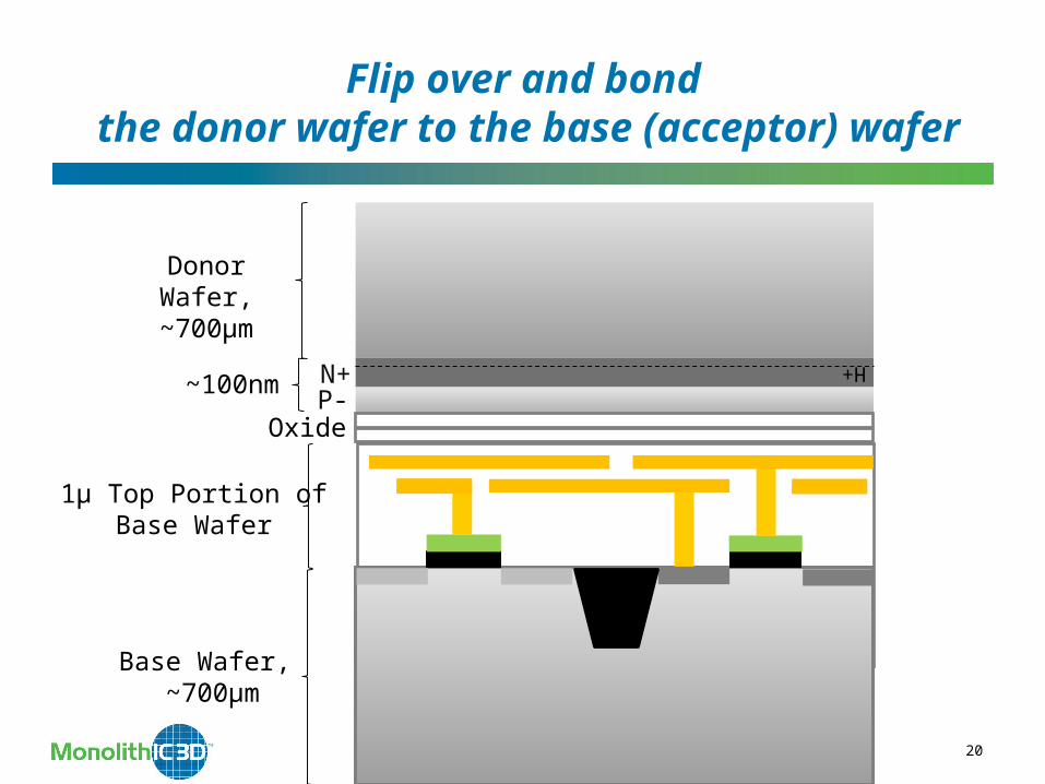
~100nm N+P-
Oxide
1µ Top Portion ofBase Wafer
H+
Flip over and bond the donor wafer to the base (acceptor) wafer
Base Wafer, ~700µm
Donor Wafer, ~700µm
MonolithIC 3D Inc. Patents Pending
21
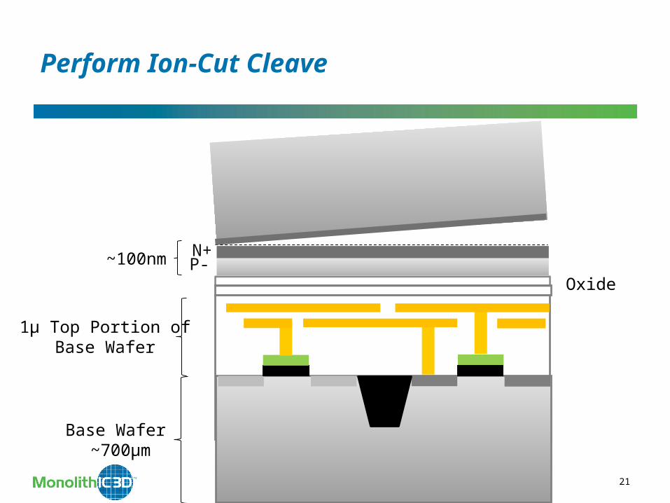
~100nm N+P-
Oxide
1µ Top Portion ofBase Wafer
Perform Ion-Cut Cleave
Base Wafer ~700µm

22
~100nm N+P-
Oxide
1µ Top Portion ofBase Wafer
MonolithIC 3D Inc. Patents Pending
Complete Ion-Cut
Base Wafer ~700µm

23
~100nm N+P-
Oxide
1µ Top Portion ofBase Wafer
MonolithIC 3D Inc. Patents Pending
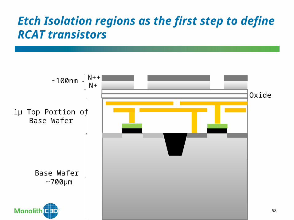
Etch Isolation regions as the first step to define RCAT transistors
Base Wafer ~700µm

24
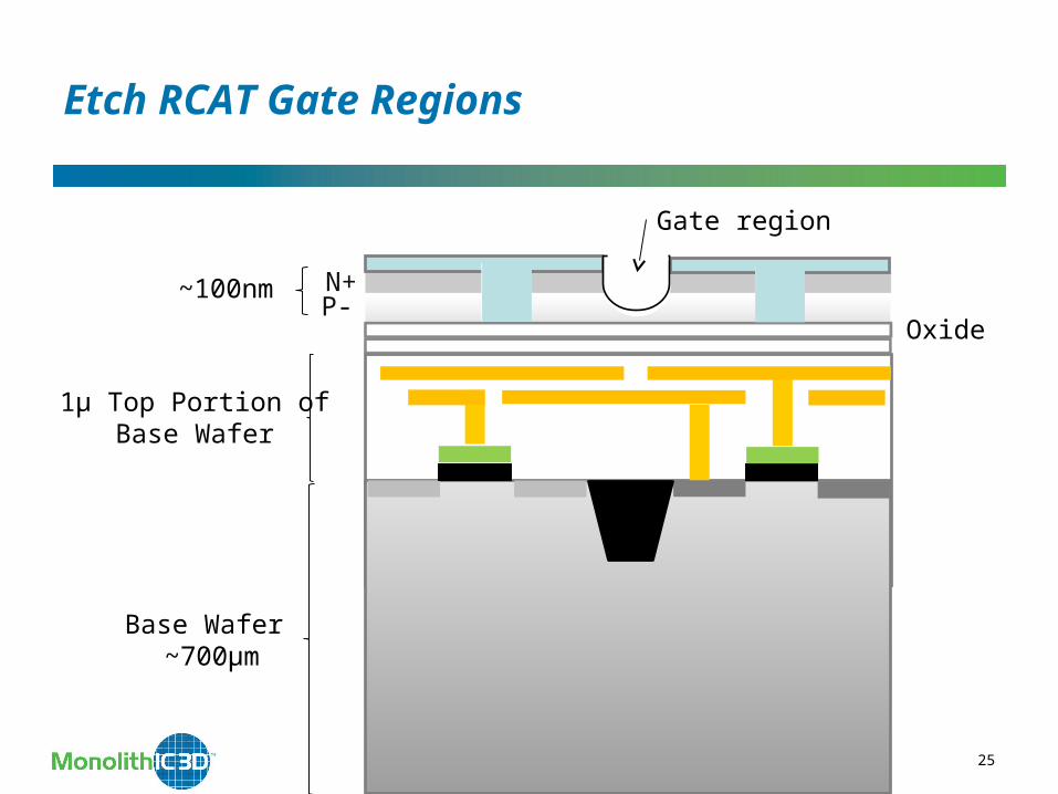
~100nm N+P-
Oxide
1µ Top Portion ofBase Wafer
MonolithIC 3D Inc. Patents Pending
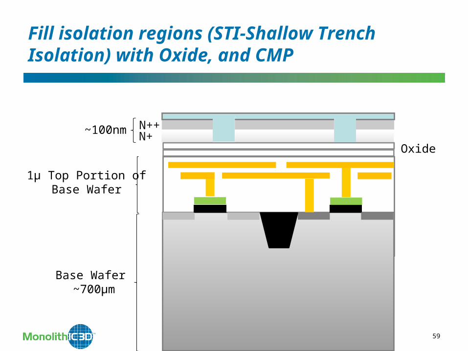
Fill isolation regions (STI-Shallow Trench Isolation) with Oxide, and CMP
Base Wafer ~700µm
25
~100nm N+P-
Oxide
1µ Top Portion ofBase Wafer
MonolithIC 3D Inc. Patents Pending
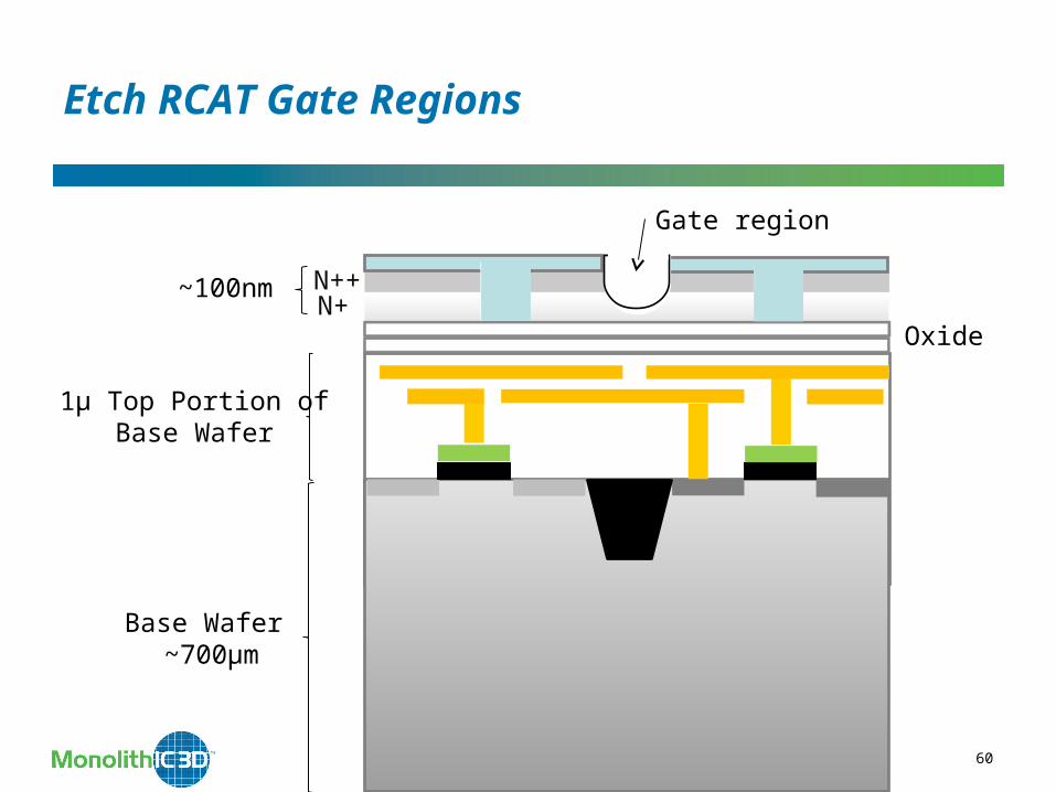
Etch RCAT Gate Regions
Base Wafer ~700µm
Gate region
26
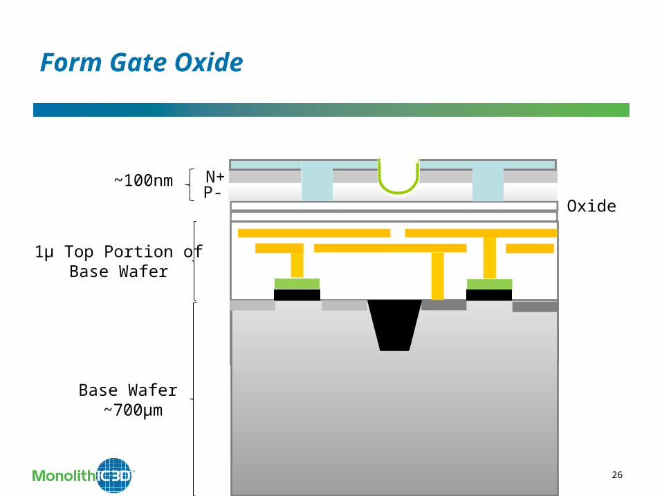
~100nm N+P-
Oxide
1µ Top Portion ofBase Wafer
MonolithIC 3D Inc. Patents Pending
Form Gate Oxide
Base Wafer ~700µm

27
~100nm N+P-
Oxide
1µ Top Portion ofBase Wafer
MonolithIC 3D Inc. Patents Pending
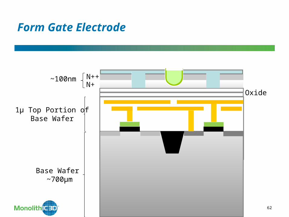
Form Gate Electrode
Base Wafer ~700µm

28
~100nm N+P-
Oxide
1µ Top Portion ofBase Wafer
MonolithIC 3D Inc. Patents Pending
Add Dielectric and CMP
Base Wafer ~700µm
29
~100nm N+P-
Oxide
1µ Top Portion ofBase Wafer
MonolithIC 3D Inc. Patents Pending
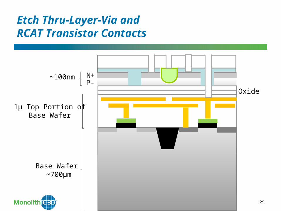
Etch Thru-Layer-Via and RCAT Transistor Contacts
Base Wafer ~700µm

30
~100nm N+P-
Oxide
1µ Top Portion ofBase Wafer
MonolithIC 3D Inc. Patents Pending
Fill in Copper
Base Wafer ~700µm

31
~100nm N+P-
Oxide1µ Top Portion of
Base (acceptor) Wafer
MonolithIC 3D Inc. Patents Pending
Add more layers monolithically
Base Wafer ~700µm
Oxide
~100nm N+P-
MonolithIC 3D Inc. Patents Pending 32
Chapter 3Monolithic 3D HKMG
MonolithIC 3D Inc. Patents Pending 33
The monolithic 3D IC technology is applied to produce monolithically stacked high performance High-k Metal Gate (HKMG) devices, the world’s most advanced production transistors.
3D Monolithic State-of-the-Art transistors are formed with ion-cut applied to a gate-last process, combined with a low temperature face-up layer transfer, repeating layouts, and an innovative inter-layer via (ILV) alignment scheme.
Monolithic 3D IC provides a path to reduce logic, SOC, and memory costs without investing in expensive scaling down.
Technology
MonolithIC 3D Inc. Patents Pending 34
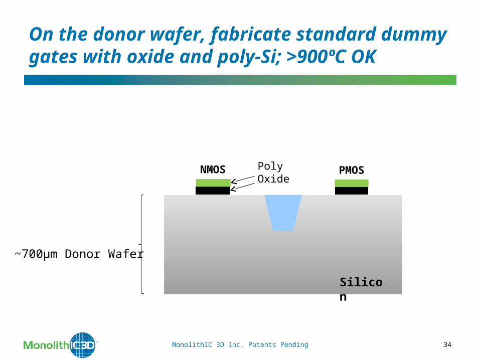
~700µm Donor Wafer
On the donor wafer, fabricate standard dummy gates with oxide and poly-Si; >900ºC OK
PMOSNMOS
Silicon
PolyOxide
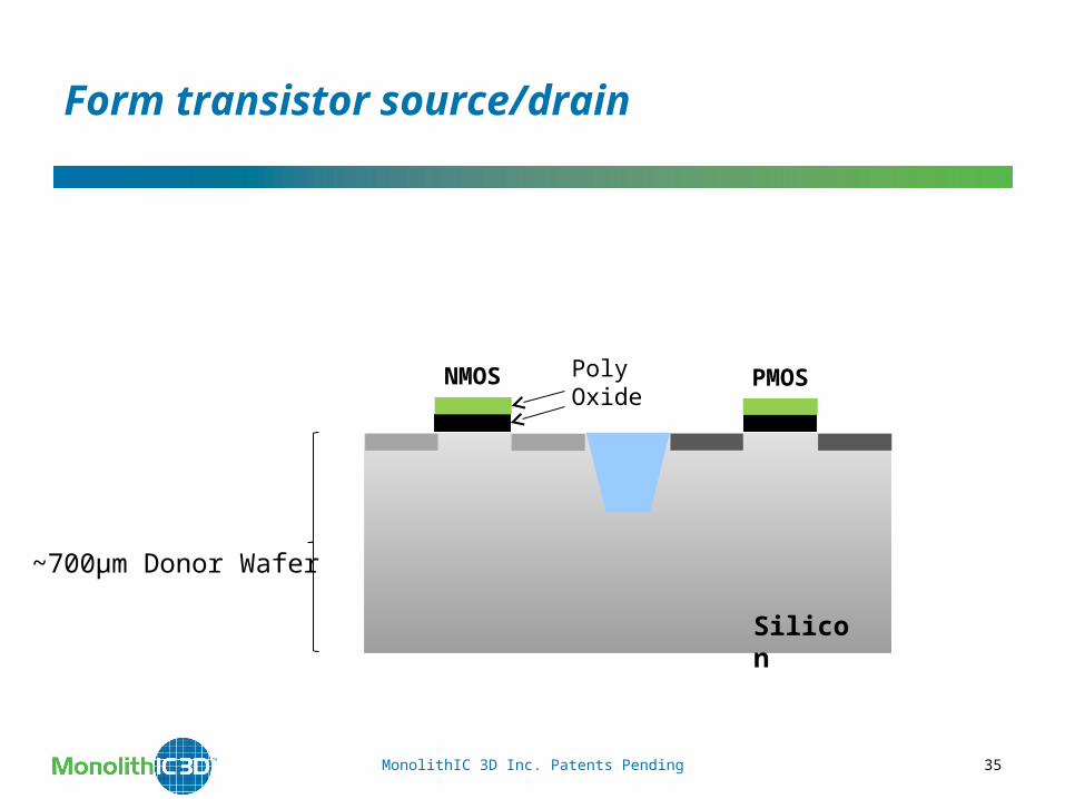
MonolithIC 3D Inc. Patents Pending 35
~700µm Donor Wafer
Form transistor source/drain
PMOSNMOS
Silicon
PolyOxide
MonolithIC 3D Inc. Patents Pending 36
~700µm Donor Wafer
PMOSNMOS
Silicon
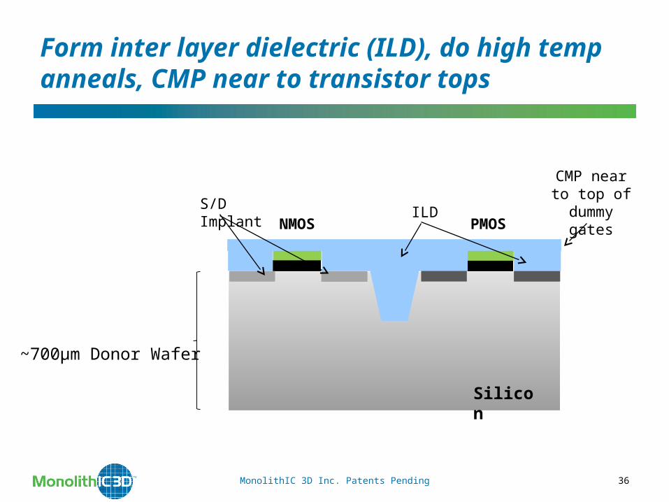
Form inter layer dielectric (ILD), do high temp anneals, CMP near to transistor tops
CMP near to top of dummy
gatesILDS/D Implant

MonolithIC 3D Inc. Patents Pending 37
~700µm Donor Wafer
PMOSNMOS
Silicon
Implant hydrogen to generate cleave plane
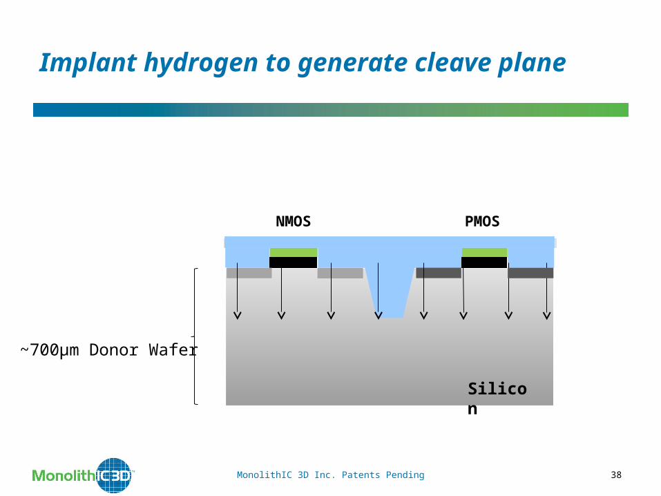
MonolithIC 3D Inc. Patents Pending 38
~700µm Donor Wafer
PMOSNMOS
Silicon
Implant hydrogen to generate cleave plane
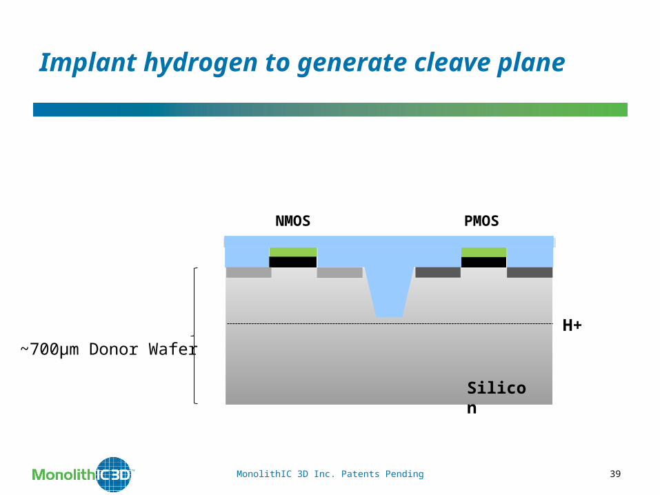
MonolithIC 3D Inc. Patents Pending 39
~700µm Donor Wafer
PMOSNMOS
Silicon
Implant hydrogen to generate cleave plane
H+
MonolithIC 3D Inc. Patents Pending 40
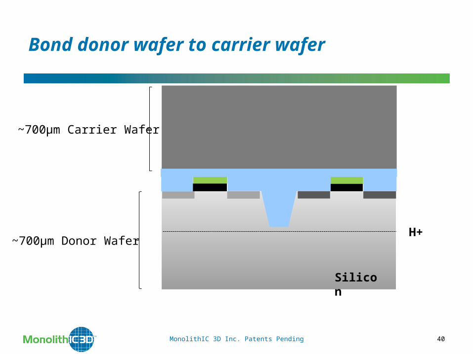
~700µm Donor Wafer
Silicon
Bond donor wafer to carrier wafer
H+
~700µm Carrier Wafer
MonolithIC 3D Inc. Patents Pending 41
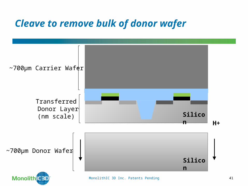
~700µm Donor Wafer
Cleave to remove bulk of donor wafer
H+
~700µm Carrier Wafer
Transferred Donor Layer
(nm scale)
Silicon
Silicon
MonolithIC 3D Inc. Patents Pending 42
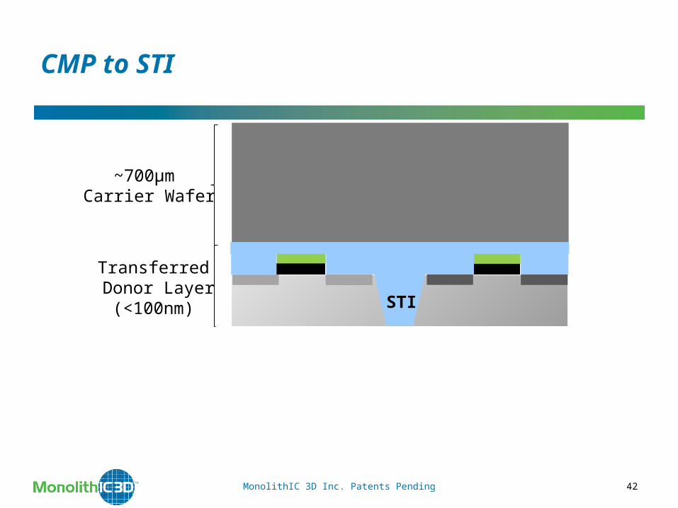
CMP to STI
~700µm Carrier Wafer
STI
Transferred Donor Layer
(<100nm)
MonolithIC 3D Inc. Patents Pending 43
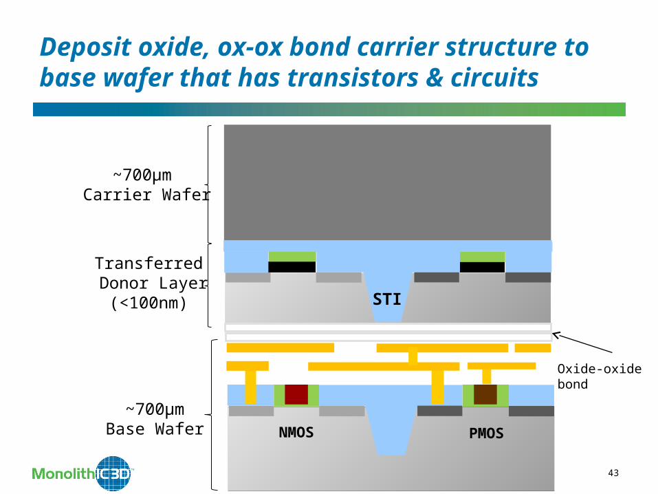
Deposit oxide, ox-ox bond carrier structure to base wafer that has transistors & circuits
~700µm Carrier Wafer
STI
Oxide-oxide bond
PMOSNMOS
~700µmBase Wafer
Transferred Donor Layer
(<100nm)
44
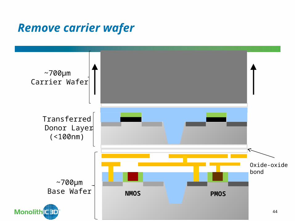
Remove carrier wafer
Oxide-oxide bond
~700µm Carrier Wafer
MonolithIC 3D Inc. Patents Pending
PMOSNMOS
~700µmBase Wafer
Transferred Donor Layer
(<100nm)
45
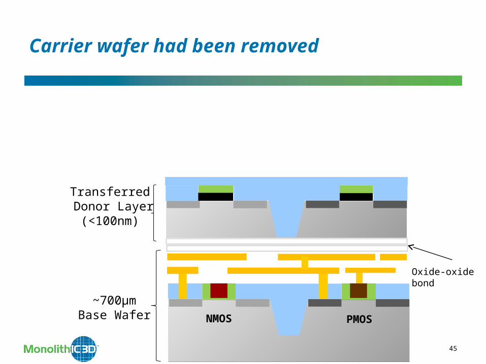
Carrier wafer had been removed
Oxide-oxide bond
MonolithIC 3D Inc. Patents Pending
PMOSNMOS
~700µmBase Wafer
Transferred Donor Layer
(<100nm)
46
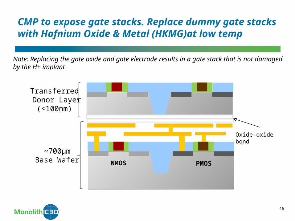
CMP to expose gate stacks. Replace dummy gate stacks with Hafnium Oxide & Metal (HKMG)at low temp
Oxide-oxide bond
MonolithIC 3D Inc. Patents Pending
PMOSNMOS
Note: Replacing the gate oxide and gate electrode results in a gate stack that is not damaged by the H+ implant
~700µmBase Wafer
Transferred Donor Layer
(<100nm)
47
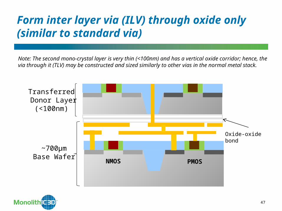
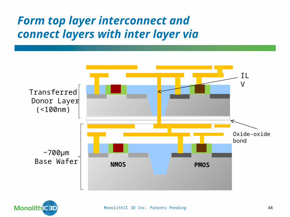
Form inter layer via (ILV) through oxide only (similar to standard via)
Oxide-oxide bond
MonolithIC 3D Inc. Patents Pending
PMOSNMOS
Note: The second mono-crystal layer is very thin (<100nm) and has a vertical oxide corridor; hence, the via through it (TLV) may be constructed and sized similarly to other vias in the normal metal stack.
Transferred Donor Layer
(<100nm)
~700µmBase Wafer
MonolithIC 3D Inc. Patents Pending 48
Form top layer interconnect and connect layers with inter layer via
Oxide-oxide bond
MonolithIC 3D Inc. Patents Pending
PMOSNMOS
ILV
Transferred Donor Layer
(<100nm)
~700µmBase Wafer
MonolithIC 3D Inc. Patents Pending 49
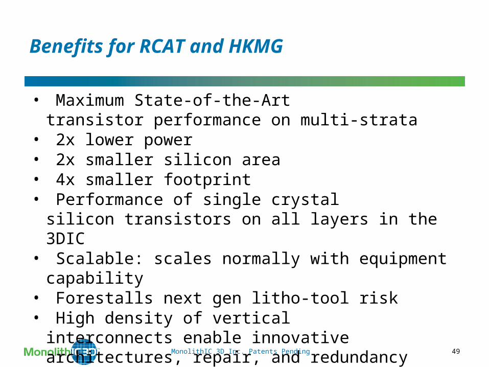
• Maximum State-of-the-Art transistor performance on multi-strata
• 2x lower power• 2x smaller silicon area• 4x smaller footprint• Performance of single crystal silicon transistors on all
layers in the 3DIC• Scalable: scales normally with equipment capability• Forestalls next gen litho-tool risk• High density of vertical interconnects enable innovative
architectures, repair, and redundancy
Benefits for RCAT and HKMG
MonolithIC 3D Inc. Patents Pending 50
Chapter 4 Monolithic 3D RC-JLT
(Recessed-Channel Junction-Less Transistor)
MonolithIC 3D Inc. Patents Pending 51
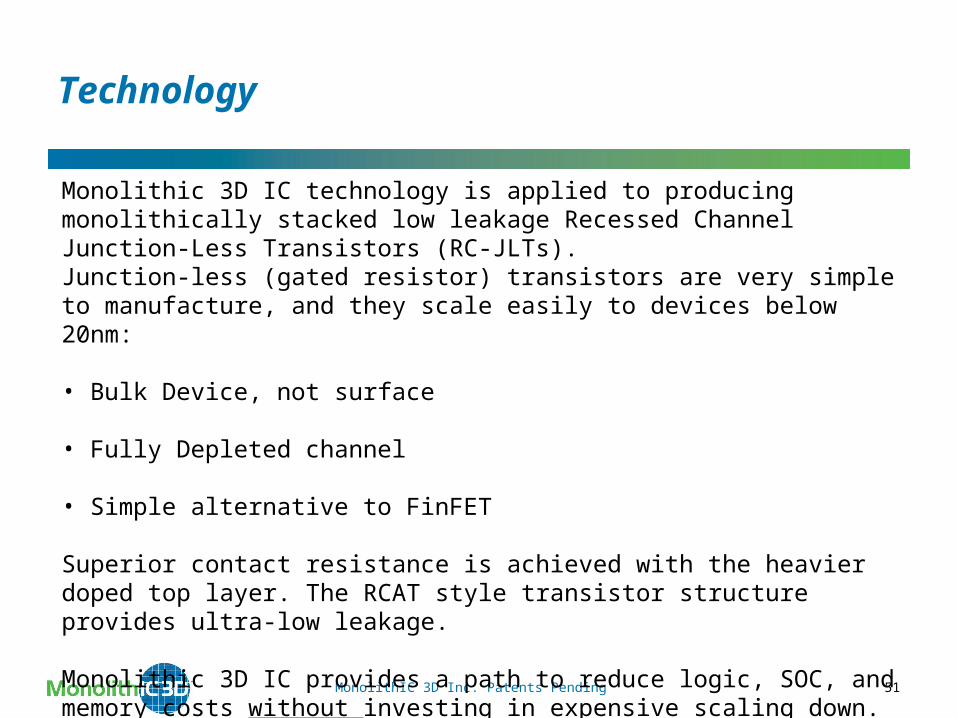
Monolithic 3D IC technology is applied to producing monolithically stacked low leakage Recessed Channel Junction-Less Transistors (RC-JLTs).Junction-less (gated resistor) transistors are very simple to manufacture, and they scale easily to devices below 20nm:
• Bulk Device, not surface
• Fully Depleted channel
• Simple alternative to FinFET
Superior contact resistance is achieved with the heavier doped top layer. The RCAT style transistor structure provides ultra-low leakage.
Monolithic 3D IC provides a path to reduce logic, SOC, and memory costs without investing in expensive scaling down.
Technology
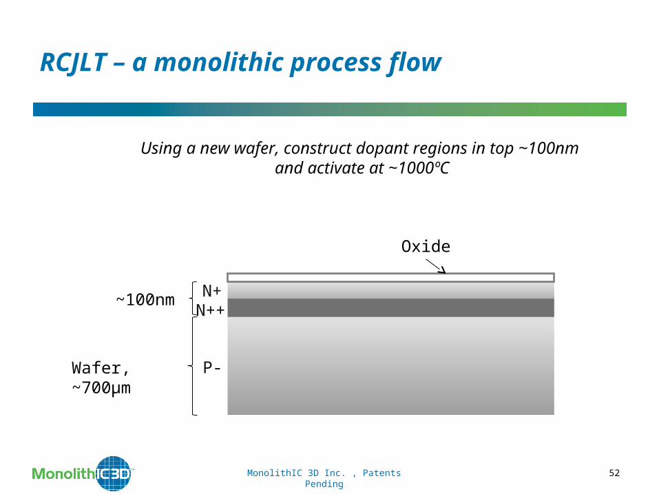
RCJLT – a monolithic process flow
MonolithIC 3D Inc. , Patents Pending 52
Wafer, ~700µm
~100nm
P-
N++N+
Using a new wafer, construct dopant regions in top ~100nm and activate at ~1000ºC
Oxide
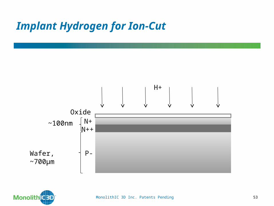
MonolithIC 3D Inc. Patents Pending 53
~100nm
P-
Oxide
Implant Hydrogen for Ion-Cut
H+
Wafer, ~700µm
N++N+
MonolithIC 3D Inc. Patents Pending 54
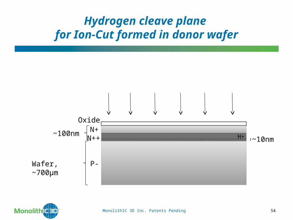
~100nm
P-
~10nm H+
Oxide
Hydrogen cleave plane for Ion-Cut formed in donor wafer
Wafer, ~700µm
N++N+

MonolithIC 3D Inc. Patents Pending 55
~100nm N++N+
Oxide
1µ Top Portion ofBase Wafer
H+
Flip over and bond the donor wafer to the base (acceptor) wafer
Base Wafer, ~700µm
Donor Wafer, ~700µm
P-

MonolithIC 3D Inc. Patents Pending
56
~100nm N++N+
Oxide
1µ Top Portion ofBase Wafer
Perform Ion-Cut Cleave
Base Wafer ~700µm
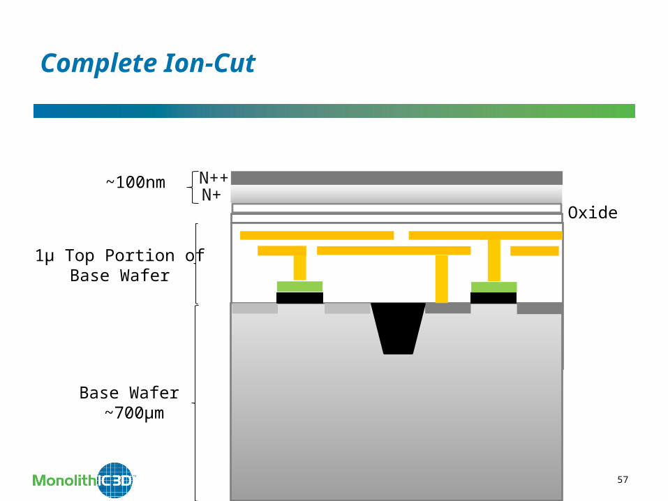
57
~100nm N++N+
Oxide
1µ Top Portion ofBase Wafer
MonolithIC 3D Inc. Patents Pending
Complete Ion-Cut
Base Wafer ~700µm
58
~100nm N++N+
Oxide
1µ Top Portion ofBase Wafer
MonolithIC 3D Inc. Patents Pending
Etch Isolation regions as the first step to define RCAT transistors
Base Wafer ~700µm
59
~100nm N++N+
Oxide
1µ Top Portion ofBase Wafer
MonolithIC 3D Inc. Patents Pending
Fill isolation regions (STI-Shallow Trench Isolation) with Oxide, and CMP
Base Wafer ~700µm
60
~100nm N++N+
Oxide
1µ Top Portion ofBase Wafer
MonolithIC 3D Inc. Patents Pending
Etch RCAT Gate Regions
Base Wafer ~700µm
Gate region

61
~100nm N++N+
Oxide
1µ Top Portion ofBase Wafer
MonolithIC 3D Inc. Patents Pending
Form Gate Oxide
Base Wafer ~700µm
62
~100nm N++N+
Oxide
1µ Top Portion ofBase Wafer
MonolithIC 3D Inc. Patents Pending
Form Gate Electrode
Base Wafer ~700µm
63
~100nm N++N+
Oxide
1µ Top Portion ofBase Wafer
MonolithIC 3D Inc. Patents Pending
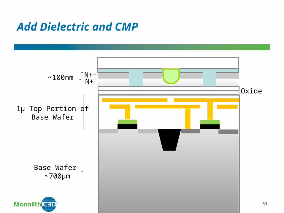
Add Dielectric and CMP
Base Wafer ~700µm
64
~100nm N++N+
Oxide
1µ Top Portion ofBase Wafer
MonolithIC 3D Inc. Patents Pending
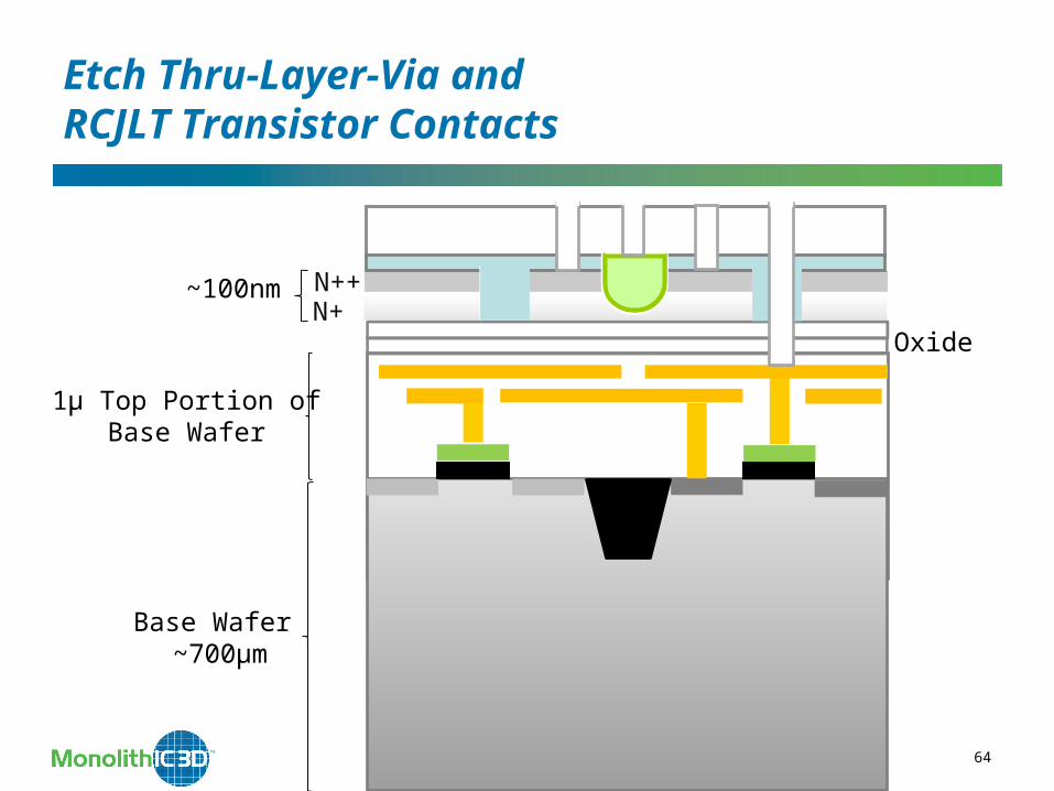
Etch Thru-Layer-Via and RCJLT Transistor Contacts
Base Wafer ~700µm
65
~100nm N++N+
Oxide
1µ Top Portion ofBase Wafer
MonolithIC 3D Inc. Patents Pending
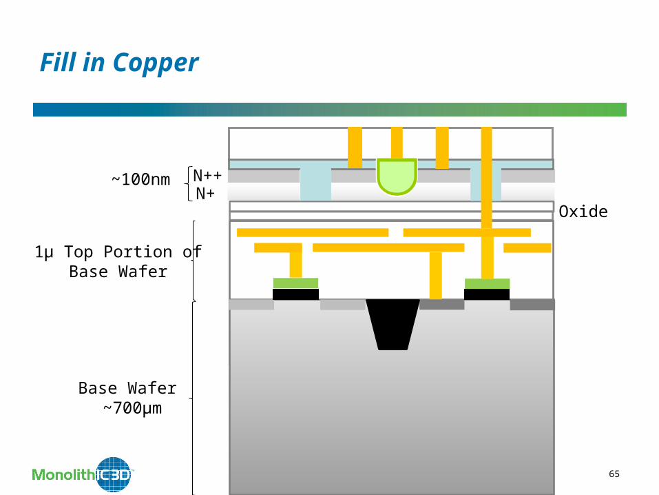
Fill in Copper
Base Wafer ~700µm
66
~100nm N++N+
Oxide1µ Top Portion of
Base (acceptor) Wafer
MonolithIC 3D Inc. Patents Pending
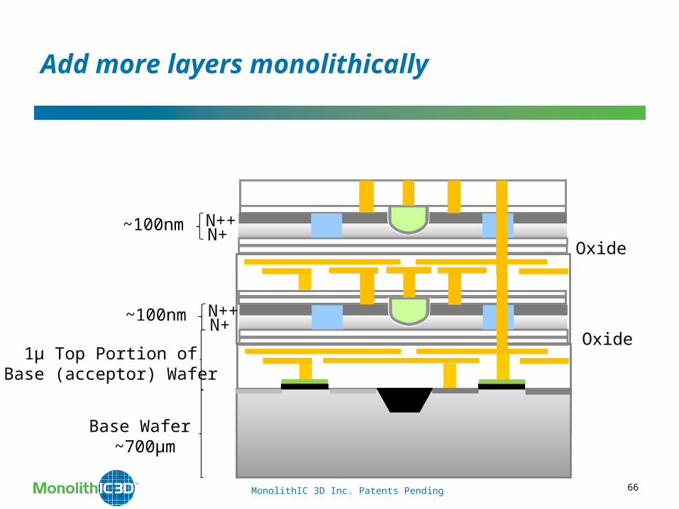
Add more layers monolithically
Base Wafer ~700µm
Oxide
~100nm N++N+
MonolithIC 3D Inc. Patents Pending 67
• 2x lower power
• 2x smaller silicon area
• 4x smaller footprint
• Layer to layer interconnect density at close to full lithographic resolution
and alignment
• Performance of single crystal silicon transistors on all layers in the 3D IC
• Scalable: scales naturally with equipment capability
• Forestalls next gen litho-tool risk
• Also useful as Anti-Fuse FPGA programming transistors: programmable
interconnect is 10x-50x smaller & lower power than SRAM FPGA
• Base logic circuits could be UT-BBOX, FinFET, or JLT CMOS logic devices
Benefits for RCJLT
MonolithIC 3D Inc. Patents Pending 68
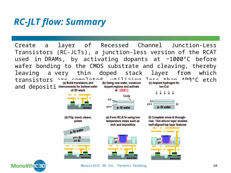
Create a layer of Recessed Channel Junction-Less Transistors (RC-JLTs), a junction-less version of the RCAT used in DRAMs, by activating dopants at ~1000°C before wafer bonding to the CMOS substrate and cleaving, thereby leaving a very thin doped stack layer from which transistors are completed, utilizing less than 400°C etch and deposition processes.
RC-JLT flow: Summary