molecular nano-electronic devices based on aharonov-bohm
TRANSCRIPT

Molecular Nano-electronic Devices
Based on Aharonov-Bohm
Interferometry
Thesis submitted for the degree of ”Doctor of Philosophy”
By:
Oded Hod
Submitted to the Senate of Tel-Aviv University
October 2005

This work was carried out under the guidance of
Professor Eran Rabani
School of Chemistry, Tel-Aviv University
and
Professor Roi Baer
Institute of Chemistry, The Hebrew University of Jerusalem
2

This work is dedicated with love to my parents Dr. Emila (Emi) Freibrun and Prof.
Israel (Izzy) Hod who made me who I am, to my wife Adi who makes me a whole person,
and to our amazing daughter Ophir for whom we live. Without your endless support and
love, this wouldn’t come true.
I am grateful to my advisors Prof. Eran Rabani and Prof. Roi Baer who showed
me ways to free my mind yet always kept the roads lighted. Due to your extraordinary
guidance, these five years have been the most wonderful intellectual experience of my life.
I would like to thank Prof. Abraham Nitzan, Prof. Ori Cheshnovsky, Prof. Mordechai
Bixon, Dr. Israel Schek, Dr. Yoram Selzer, Dr. Michael Gozin, and Barry Leibovitch for
fruitful suggestions and discussions.
I would also like to thank my wonderful aunt Miri and my wonderful siblings Sivan
Hod, Dr. Shahar Hod and Dr. Nir Hod for their support and help at all times.
With a lot of appreciation I thank my second father and mother - Marta (Matti) and
Pinchas Zalckvar and the wonderful Einat and Noa for always being there to offer their help.
Many thanks to my friends from the group: Nurit Shental, Claudia G. Sztrum, Guy
Yosef, Guy Cohen and Orly Kletenik for intriguing scientific and personal discussions who
enriched my life.
3

I. ABSTRACT
The quest for understanding the physical principles governing sub-micronic and low di-
mensional systems has gained vast attention in modern physics. The invention of imaging
technologies with nanometer scale resolution has opened the way for exciting scientific and
technological possibilities. One major field which has recently developed immensely is the
field of molecular electronics. From a scientific point of view this field has received a lot of
experimental and theoretical interest. While new revolutionary experimental technologies
allow the measurement of the physical properties of entities as small as a single molecule, or
even a single atom, the related theories enable the utilization of highly accurate, state of the
art, computational methods. Therefore the field of molecular electronics encourages an inti-
mate synergic cooperation between experimentalists and theorists. The technological aspect
involves the possible utilization of the unique physical properties of small scale systems for
the fabrication of miniature new electronic and mechanical devices. This is expected to be
a very important technological issue in the near future when existing electronic technologies
are predicted to be exhausted.
A major goal of molecular electronics is to gain control over the conductance through a
single molecule. An effective way suggested to control the conductance through micrometer
scale loops is the application of a magnetic field threading the cross section of the ring.
This effect, attributed to Y. Aharonov and D. Bohm, was intensively explored in mesoscopic
physics studies. A natural extrapolation of these ideas to cyclic molecular devices was
considered to be prohibited due to the extremely high magnetic fields expected to be involved
in the control process.
The objective of the present research is to define the physical problem of utilizing, or
even studying, the Aharonov-Bohm effect in scales much smaller than the microscale and to
suggest an answer to this problem. This objective is important not only on a pure scientific
ground but also when regarding the possible technological outcomes.
In order to fulfill this objective we use a one-dimensional continuum model of a nanome-
ter scale Aharonov-Bohm interferometer, which is based on scattering matrix techniques.
Even though very simplistic this model captures the essential physics and allows the iso-
lation and systematic study of the important physical parameters that are crucial to gain
controllable transport through miniature conducting loops. The continuum model results
4

suggest that despite of the nanometer scale cross section of the regarded systems, extremely
high sensitivity to external magnetic fields can be achieved. The basic idea is to weakly
couple a nanometric cyclic molecule/setup to two conducting leads, thus forming a resonant
tunneling junction in which conductance occurs only through the well defined resonances of
the ring. By applying a gate voltage to the ring, one can control the conducting electrons
momentum and tune the system to be highly conductive at the absence of a magnetic field.
Turning on a relatively low magnetic field will then shift the doubly degenerate narrow en-
ergy levels of the ring out of resonance with the leads and thus the conductance will drop
sharply.
We test the predictions of the continuum model on realistic, pre-designed, molecular se-
tups using an atomistic computational model developed for this purpose. This model is
based on the semi-empirical extended Huckel approach which is properly adjusted for the
calculation of the electronic structure of the molecule under the influence of an externally
applied magnetic field. We use non-equilibrium Green’s function formalism to calculate the
conductance through the molecular setup in the presence of the magnetic fields. In the
absence of inelastic scattering this reduces to the Landauer formula which relates the con-
ductance to the transmission probability of an electron through the molecular frame. The
transmission probability is in turn calculated using scattering theory approaches such as
Green’s function techniques and absorbing imaginary potentials methods. The results ob-
tained by the atomistic calculations are found to be fully reproducible by a single parameter
fit of the continuum model.
After exploring two terminal interferometers using the methodology described above, an
expansion of the continuum model to the three terminal case is presented. It is found that in
such a setup the symmetry breaking nature of magnetic fields allow the selective control of
the electrons outgoing route. This property is unique to magnetic fields and similar effects
cannot be obtained by the application of external electric fields. Based on this concept a
molecular logic gate that processes two logic operations simultaneously is presented.
The rule of Inelastic scattering on the electrons dephasing is studied within the framework
of non equilibrium Green’s function formalism. A model which locally couples the conducting
electrons to the vibrations of the device atoms is presented. Using the Born approximation
we find that at the low coupling regime the magneto-conductance sensitivity increases. This
behavior is opposite to the gate dependent conductance which becomes less sensitive to
5

changes in the gate potential when the coupling to the vibrations is turned on. Different
coupling strengths and temperature dependence are studied.
Possibilities for further investigation in the directions of inelastic scattering effects in the
high coupling regime, particles spin effects, and electron versus hole magneto-conductance
are discussed.
6

Contents
I. Abstract 4
II. Introduction 9
A. Thesis Outline 15
III. Defining the open question 18
A. Basic concepts - Aharonov-Bohm interferometry 18
B. Length Scales 21
1. Fermi de-Broglie wave length 22
2. Mean free path 22
3. Coherence length scale 23
C. The open question 23
IV. Continuum Model 26
V. Why Use Magnetic Fields? 34
VI. Atomistic Calculations - model 40
A. Conductance 40
B. Retarded and advanced Green’s functions and self energies 43
C. An alternative - Absorbing imaginary potentials 46
D. Electronic structure - Magnetic Extended Huckel Theory 48
VII. Atomistic calculations - results 51
A. Atomic corral 51
B. Carbon Nanotubes 57
C. Three terminal devices based on polyaromatic hydrocarbon rings 64
D. Temperature effects - Broadening of the Fermi-Dirac distributions 68
VIII. Inelastic scattering effects - Model 70
A. Hamiltonian 70
1. The electronic Hamiltonian 70
2. The vibrational Hamiltonian - Normal modes of an atomic chain 71
7

3. The electron-vibrations interaction term 74
4. The full Hamiltonian 74
B. conductance 75
C. Self consistent Born approximation 76
D. First Born approximation 77
E. Numerical considerations 78
IX. Inelastic scattering effects - Results 82
X. Summary and prospects 88
A. Analytic expressions for the overlap integrals over real Slater type
orbitals 92
1. single center overlap integrals 92
2. Two coaxial center overlap integrals 93
3. General overlap integrals 95
B. Magnetic terms integrals over real STOs as linear combinations of
overlap integrals 96
1. Linear magnetic term integrals 97
2. Quadratic magnetic term integrals 101
References 109
8

II. INTRODUCTION
It was in 1959 that Richard Feynman, in his far-seeing lecture ’There’s Plenty of Room
at the Bottom’, realized that one of the most technologically promising and scientifically
interesting unexplored field in physics involves the ability to manipulate and gain control
over miniature structures:
’... I would like to describe a field, in which little has been done, but in which an enormous
amount can be done in principle. This field is not quite the same as the others in that it
will not tell us much of fundamental physics ... but ... it might tell us much of great interest
about the strange phenomena that occur in complex situations. Furthermore, a point that is
most important is that it would have an enormous number of technical applications.
What I want to talk about is the problem of manipulating and controlling things on a
small scale. ...’
This call for multidisciplinary involvement in the study of the manufacturing and control
at miniature length scales served to attract attention to a field which has since developed
rapidly to be the cutting edge of technology and scientific interest these days.
Nevertheless, the chemical foundations of molecular electronics are considered, by field
specialists1, to be planted two decades ahead of Feynman’s visionary statement. It was
Mulliken2 who in the late 1930’s commenced studies on the spectroscopy of intra-molecular
charge transfer. This led to a massively addressed research domain of Donor-Acceptor com-
plexes charge transfer chemistry3–10 which eventually set the foundation for the cornerstone
of molecular electronics attributed to Aviram and Ratner11. In a novel theoretical predic-
tion, made in 1974, they suggested that A Donor-Bridge-Acceptor type molecule could, in
principle, act as a molecular rectifier. What designates this study is the fact that for the
first time a single molecule was considered to act as an electronic component rather
than just being a charge transfer medium. Therefore, it could serve as a potential building
block for future miniature electronic devices. It should be noted that 25 years have passed
before experimental evidence12 of molecular rectification based on the Aviram-Ratner idea
became available.
One of the most fundamental difficulties in the actual implementation of Aviram and
Ratner’s ideas was the inability to ’see’ at the molecular scale. Without seeing it is im-
possible to create, characterize and examine such miniature devices. A major technological
9

breakthrough that suggested a solution to this problem was the invention of the Nobel
prize awarded scanning tunneling microscope∗ in 1981† by H. Rohrer and G. Binnig13,14, fol-
lowed by several atomic resolution imaging technologies such as Atomic Force Microscopy15.
These inventions allowed for the simultaneous and direct characterization, manipulation
and tunneling current measurements of atomic and molecular species on well defined sur-
faces, enabling the design and investigation of the electronic properties of artificially created
structures16–18.
FIG. 1: Quantum corral structure made by STM tip manipulation of Iron atoms on a Copper (111)
surface (taken from [19] and [16]).
Currently, single molecule electronics20–31 is a rapidly growing scientific field. In recent
years, a number of experimental techniques have been developed to synthesize molecular
junctions and measure their conductance as a function of an externally applied bias. These
technologies include mechanically controllable break junctions32–35, electro-migration break
junctions36–38, electron beam lithography39,40, shadow evaporation41,42, electrochemical de-
position43–45, mercury droplet technologies46–48, cross-wire tunnel junctions49, STM50,51 and
conducting AFM52 tip measurements, placing long nanowires on top of conducting elec-
trodes53, and additional methods54.
These remarkable achievements allow for the construction of fundamental molecular de-
vices and for the characterization of their electronic and electric properties. However, since
∗ which perhaps more appropriately should be referred to as a nanoscope rather than a microscope.† Earlier attempts to build a similar device which were conducted by Russell Young of the U.S. National
Bureau of Standards beginning at 1965 ended in failure due to unresolved vibrational issues.
10

(a) (b) (c)
FIG. 2: Several examples of molecular junctions. (a) A schematic representation of a benzene-1,4-
dithiolate molecule trapped in a mechanically controllable break junction (taken from [32]). (b) A
∼ 1nm gold junction formed by electro-migration technique on an aluminum oxide gate electrode
(taken from [37]). (c) A carbon nanotube placed on a Si/SiO2 substrate between two platinum
electrodes (taken from [53]).
such technologies are still immature, they encounter fabrication and measurement repro-
ducibility problems sometimes followed by harsh criticism55.
Such experimental complexities accompanied by the accessibility to the utilization of
highly precise and powerful computational methods (due to the smallness of the physical
systems considered), make molecular electronics an extremely appealing theoretical field of
research. This allows not only the clarification and understanding of existing experimental
data but also the ability to predict and design of future molecular devices.
An important contribution to the theoretical investigation of electron current flow through
molecular scale systems was made by Rolf Landauer56 in 1957. Landauer directly related
the conductance through a system, which is coupled to two leads, to the (energy depen-
dent) probability amplitude of an electron approaching the system from one of the leads to
be transmitted to the other lead. By this he effectively reduced the problem of coherent
conductance to a well defined elastic scattering theory problem, thus giving a microscopic
description of the conductance process. The utilization of Landauer’s formalism with a
combination of simple continuum/tight-binding57–62 models or very sophisticated methods
such as ab-initio based Green’s function techniques63–70 is the main tool for investigating
the conductance through molecular systems up to this day. Recently, quantum dynamical
approaches such as time dependent density functional theory investigations71–75 and related
11

methods76,77 were used for the evaluation of molecular conductance.
Interestingly, at the very same year that Feynman approached the scientific community
with the urge to investigate the ’bottom’, a seminal work by Yakir Aharonov and David
Bohm78 was published regarding the ’Significance of Electromagnetic Potentials in the Quan-
tum Theory’‡. Using two gedanken-experimental setups, one involving electric fields and the
other one magnetic fields, Aharonov and Bohm were able to prove that the fundamental en-
tities in quantum mechanics are the electromagnetic potentials. Moreover, they have shown
that electromagnetic fields or forces often considered in classical electrodynamics are not
adequate from a full quantum mechanical point of view.
The main result of the Aharonov-Bohm (AB) theory is the fact that a charged particle is
affected by electromagnetic fields even if they are applied in regions from which the particle
itself is excluded. This was theoretically demonstrated for an electronic version of the double-
slit experiment, in which a singular magnetic field is applied in the center point between
the two slits and perpendicular to the plane of the electrons motion (see Fig. 4). Since the
magnetic field is excluded from the electrons pathways, a classical charged particle would
not feel its existence. However, a quantum mechanical particle is predicted to experience a
phase shift. Due to the fact that the sign of this phase shift depends on whether the particle
moves clockwise or counterclockwise in the magnetic field, an observable alternation in the
interference pattern is obtained by the application of the magnetic field. This alternation is
found to be periodic with a period proportional to the magnetic flux threading the circular
electrons pathway. Therefore, allowing for the alternate switching of the interference pattern
at a given point on the screen between constructive and destructive interference. It should
be noted that since the treatment is based on interference effects it is required that the beam
of incoming electrons would be coherent in such a sense that the momentum and the phase
of the electrons would be well defined.
Shortly after their theoretical prediction, an experimental verification80 using vacuum
propagating electron waves was available for the AB effect. Nevertheless, even though a
great deal of related experimental81–95 and theoretical96–103 studies have been conducted
since, only a quarter of a century later a realization which seemed appropriate for electronic
‡ Preliminary discussions considering the role of potentials in quantum mechanics can already be found as
early as 1949.79
12

conductance switching was presented. Using a sub-micronic fabricated polycrystalline gold
ring coupled to two conducting wires (see Fig. 3) and threaded by an external magnetic field
at sub-Kelvin temperatures, Webb el al104 were able to measure periodic magnetoresistance
oscillations with a period of the order of ∼ 1×10⁻² Tesla and an amplitude of about 0.05Ω.
FIG. 3: Aharonov-Bohm magnetoresistance periodic oscillations measured for a polycrystalline
gold ring with an inner diameter of 784 nm at a temperature of 0.01K (taken from [104]).
This setup can be viewed as a prototype of a sub-micronic field effect transistor in which
the role of the gate control is taken by the external magnetic field. However, even at very low
temperatures, such a micrometer scale ring cannot be considered as a coherent conductor.
This provides an explanation to the fact that the amplitude of the AB oscillations, observed
in Fig. 3 is quite damped.105
A natural goal, therefore, would be to miniaturize such a device and make it operable at
length scales much smaller than the electrons decoherence length scales. One may naively
conclude that the miniaturization of an AB interferometer, based on the setup created by
Webb et al,104 into the nanoscale is purely an engineering fabrication challenge. However, a
fundamental physical limitation prevents the observation of the AB effect in the nanoscale.
This limitation results from the fact that the period of the magnetoresistance oscillations is
proportional to the magnetic flux threading the ring, as mentioned above. Therefore, the
period of the oscillations for a ring with a diameter of the order of a single nanometer should
13

be six orders of magnitude larger than that of a micrometer scale ring. Considering the
magnetoresistance oscillations measured by Webb et al for a micrometer ring, the predicted
period of a nanometer scale ring is of the order of ∼ 1 × 10⁴ Tesla - much larger than the
magnetic field regime limit achievable in modern laboratories (∼ 5 × 101 Tesla). Therefore,
it is widely accepted that AB interferometry at the nanometer scale regime is not feasible.
Nevertheless, in recent years there have been several experimental realizations of magnetic
field effects in nanometer scale structures. The major part of these regard Zeeman splitting
of spin states in quantum dots106 and in carbon nanotubes53,107,108, and the Kondo effect
measured for mesoscale quantum dots,109,110 fullerenes,111–114 and single molecules.37,40 Other
magnetic effects in quantum dots115,116 and in carbon nanotubes117 where also observed. Yet,
most of these still involve basic physics research and are currently not aimed for technological
applications.
In this context, it is important to remember that a major propellant for the ongoing
development of nanotechnology is the strive to miniaturize current electronic devices in order
to gain higher computational efficiency. Miniaturization limitations of current state of the art
microelectronic technologies impel the advancement of alternatives. This is best expressed in
a statement made by Mark Reed at the third international conference on molecular electronic
devices, held at Arlington, Virginia, in October 1986:1,118
‘...The exponential growth in the semiconductor electronics industry is attributed to
schemes that permit the physical downscaling of transistor-based ICs. This downscaling
capability will eventually be brought to an end by the barriers of device scaling limits, in-
terconnection saturation and yield. Achievement of limiting geometries from historical ex-
trapolation will occur in the mid-1990s. If there is to be a post VLSI technology, it must
employ simultaneously revolutionary solutions in design, architecture, and device physics to
circumvent the interconnection problem. ...’
This predicted breakdown of Moore’s law, even though a decade later than Reed’s pre-
diction, is starting to be felt in current CPU performance advancement rates. Therefore,
stressing the need to further invest scientific and technological efforts in the development and
implementation of revolutionary ideas for future electronic devices based on nanotechnology
and molecular electronics. An exceptional example for such novel efforts can be found in the
fascinating and growing field of spintronics.119–127 While in conventional electronics infor-
mation is carried by the charge of electrons it is suggested that electrons spins can serve as
14

information carriers enabling faster and more efficient ways for data processing and storage.
The purpose of this thesis is to suggest a way to circumvent the intrinsic physical restric-
tion that limits the utilization of magnetic interferometry to the micrometer scale, and to
identify the physical conditions that enable the miniaturization of magnetoresistance elec-
tronic devices, based on such effects, to the nanometer/molecular scale. At that scale the
clear advantages of coherent transport, quantum confinement and device reproducibility are
expected to result in a pronounced effect. The essential procedure involves the weak cou-
pling of the conducting leads to the interferometric ring, thus creating a resonant tunneling
junction in which the conductance is allowed only through the narrow, doubly degenerate,
energy levels of the ring. A gate voltage is used to tune the ring Fermi energy so that at a
zero magnetic flux the conductance is high. The application of a relatively low (compared to
the full AB period) external magnetic field, consequently shifts the narrow energy levels of
the ring out of resonance and thus switches the conductance off. § Based on these principles,
architectures that both mimic conventional electronics and allow for new computational
schemes will be explored.
A. Thesis Outline
The next chapter is dedicated to the definition of the open question. A short mathematical
description of the interactions of electrons with electromagnetic fields in the context of
magnetoresistance interferometry is given in section IIIA. Within this description the major
differences between the classical and the quantum mechanical treatment of external fields
and potentials are stressed. The relevant length scales that set upper limits to the regime at
which Aharonov-Bohm interferometry is feasible are discussed in section IIIB. Finally, in
section IIIC the open question, studied in the subsequent chapters of the thesis, is defined.
In chapter IV a one-dimensional (1D) scattering theory continuum model of an AB in-
terferometer is introduced. The model assumes that the charge carrying particles have well
defined momentum and phase and that their transport along the interferometer is ballistic
except for two well defined elastic scattering centers. This simplistic model allows the iden-
tification and isolation of the crucial physical parameters that allow the miniaturization of
§ It should be mentioned that resonant tunneling has been previously utilized, through a different mecha-
nism, as a sensitive probe in AB mesoscopic two dimensional electron gas experimental setups.128–130
15

magnetoresistance interferometric devices into the nanoscale.
The advantages of using magnetic fields in nanometer scale electronics are presented in
chapter V. This is achieved by expanding the two-terminal continuum model, described in
chapter IV, to the three terminal AB interferometer case. It is shown that the magnetic field
polarity becomes an important control parameter which allows the selective switching of the
conducting electrons outgoing channel. This behavior is found to be unique to magnetic
fields due to their symmetry breaking nature.
After identifying and studying the conditions at which AB interferometry at the nanoscale
is expected to be feasible using the simplistic physical continuum model, I turn in chapter VI
to present the Magnetic Extended Huckel Theory (MEHT) atomistic model developed for the
direct calculation of the conductance through molecular junctions under the influence of an
externally applied magnetic field. In section VIA an outline of the essential non-equilibrium
Green’s function formalism relations required for the calculation of the conductance is given.
At the limit of coherent transport, these equations are shown to reduce to the two terminal
Landauer formula. The calculation of the Green’s functions and self energies (SEs) appearing
in the conductance formulas is discussed in section VIB. This is followed by an alternative
route for the conductance calculation using absorbing potentials boundary conditions which
is given in section VIC. All these calculations are based on the information gained from the
electronic structure of the system. Section VID is devoted to the electronic structure calcu-
lation of the different parts of the system. A description of the model Hamiltonian, based
on the addition of the appropriate magnetic terms to the extended Huckel Hamiltonian, is
given therein.
In chapter VII the MEHT calculation results are presented for three different molecular
setups. First considered (VIIA) is an atomic corral coupled to two atomic wires, placed
on a semi-conductor surface, and threaded by a perpendicular magnetic field. This setup
mostly resembles the 1D continuum model and the corresponding results are shown to be
fully reproducible by a single parameter fit of the continuum model. Next, in section VIIB,
a nanometer scale molecular switch based on the AB effect in carbon nanotubes (CNTs)
is presented. Two experimental setups are suggested: in the first a CNT is placed on an
insulating surface in parallel with two conducting electrodes and in the second a CNT is
placed on a conducting surface and approached by a STM tip from above. The conductance
through the circumference of the CNT can then be controlled by the application of a mag-
16

netic field parallel to the main axis of the CNT. In section VIIC a three terminal device
composed of a polyaromatic hydrocarbon ring coupled to three gold atomic wires is stud-
ied. Similar to the predictions of the continuum model, it is found possible to control the
outgoing route of the electrons by changing the polarity of the magnetic field. A truth table
is constructed in which each of the outgoing channels processes a different logic operation
simultaneously. To conclude this chapter an analysis of the temperature dependence of the
reported calculation results is presented in section VIID.
An expansion of the atomistic calculations model to include inelastic scattering effects is
presented in chapter VIII. In section VIIIA the model Hamiltonian which includes inelastic
scattering effects is presented. The corrections to the conductance formulas in the case of
electron-vibrations interactions are given in section VIIIB. Approximate ways to solve the
many body problem involved in the conductance calculations are outlined in sections VIIIC
and VIIID. This is followed by the presentation of a truncation procedure, in section VIII E,
which allows the reduction of the computational efforts considerably. It is shown that using
this procedure the conductance calculation becomes independent of the size of the device.
In chapter IX the results of the atomistic calculations in the case of electron-vibrations
interactions are given. First, the dependence of the zero-bias and zero magnetic field con-
ductance through an atomic corral on an applied gate voltage is studied. A comparison
between the case of pure coherent transport and the case of transport in the presence of
electron-vibrations interactions is given, showing that the line-shape width is broadened due
to the vibrational coupling. Similar results are obtained for a phenomenological model of a
single level coupled to a single vibrational mode. Next we consider the magneto-conductance
spectrum dependence on the vibrational coupling strength. We find that at a temperature
of 1K the magneto-conductance becomes more sensitive to the applied magnetic field upon
switching on the coupling with the vibrational modes of the molecule. A similar picture is
found for a higher temperature of 10K.
Finally, a summary in which future directions are discussed is given in chapter X.
There are two appendices to this thesis. In appendix A we present, for the sake of com-
pleteness, the expression for the analytical evaluation of Slater type orbitals overlap integrals,
which are used within the MEHT method. Appendix B is devoted to the development of
the expansion of relevant magnetic integrals in terms of overlap integrals, allowing for the
analytical evaluation of the MEHT magnetic terms as well.
17

III. DEFINING THE OPEN QUESTION
A. Basic concepts - Aharonov-Bohm interferometry
In classical mechanics the force exerted on a charged particle transversing a region in
space which incorporates an electric and/or a magnetic field is given by the Lorentz force
law F = q(E + v × B), where q is the charge of the particle, E is the electric field, v is the
particle’s velocity, and B is the magnetic field. It can be seen that the electric field operates
on a particle whether static or not and contributes a force parallel to its direction and
proportional to its magnitude, while the magnetic field operates only on moving particles
and contributes a force acting perpendicular to its direction and to the direction of the
particles movement. When solving Newtons equation of motion F = dPdt
, the resulting
trajectories for a classical charged particle entering a region of a uniform magnetic field will
thus be circular. We can define scalar and vectorial potentials using the following definitions
E(r, t) = −∇V − ∂A(r,t)∂t
and B(r, t) = ∇×A(r, t), respectively. When defining the following
Lagrangian L = 12mv2 − qV (r) + qv · A, and deriving the canonical momentum using the
relation Pi = ∂L∂ri
one can, in principle, solve the Euler-Lagrange or Hamilton equations
of motion. This procedure, even though easier to solve for some physical problems, is
absolutely equivalent to solving Newton equations of motion and will produce the exact
same trajectories.
The influence of electric and magnetic fields on the dynamics of quantum charged particles
was investigated by Aharonov and Bohm in a seminal work from 195978 revealing one of
the fundamental differences between the classical and the quantum description of nature.
According to Aharonov and Bohm, while in classical mechanics the transition from using
electric and magnetic fields to using scalar and vectorial potentials is “cosmetic” and may be
regarded as a mathematical pathway for solving equivalent problems, in quantum mechanics
the fundamental quantities are the potentials themselves.
In order to demonstrate this principle consider a double-slit experiment applied to elec-
trons as seen in Fig. 4. The experimental setup consists of a source emitting coherent
electrons which are diffracted through two slits embedded in a screen. The electron inten-
sity is measured in a detector placed on the opposite side of the screen. In the absence of a
magnetic field the intensity measured by the detector when placed directly opposite to the
18

FIG. 4: The Aharonov-Bohm double-slit experiment setup for charged particles.
source will be maximal due to the positive interference between the two electron pathways
which are of equal length. When applying a point magnetic field perpendicular to the inter-
ference plane, as indicated in Fig. 4, the interference intensity is altered. Unlike the classical
prediction, this change in the interference pattern is expected even if the magnetic field is
excluded from both electron pathways. This can be traced back to the fact that even tough
the magnetic field is zero along these pathways, the corresponding vector potential does not
necessarily vanish at these regions.
In order to give a more quantitative description of this phenomena we consider an anal-
ogous model consisting of a ring shaped ballistic conductor forcing the bound electrons to
move in a circular motion connecting the source and the detector as shown in Fig. 5.
The Hamiltonian of the electrons under the influence of electric and magnetic potentials ¶
is given by:
H =1
2m
[P− qA(r)
]2
+ V (r). (1)
Here m is the mass of the particle, P = −i~∇ is the canonical momentum operator, and ~ is
Plank’s constant divided by 2π. In the absence of electrostatic interactions, the Hamiltonian
¶ Field quantization is disregarded in the entire treatment and we assume that the potentials are time
independent.
19
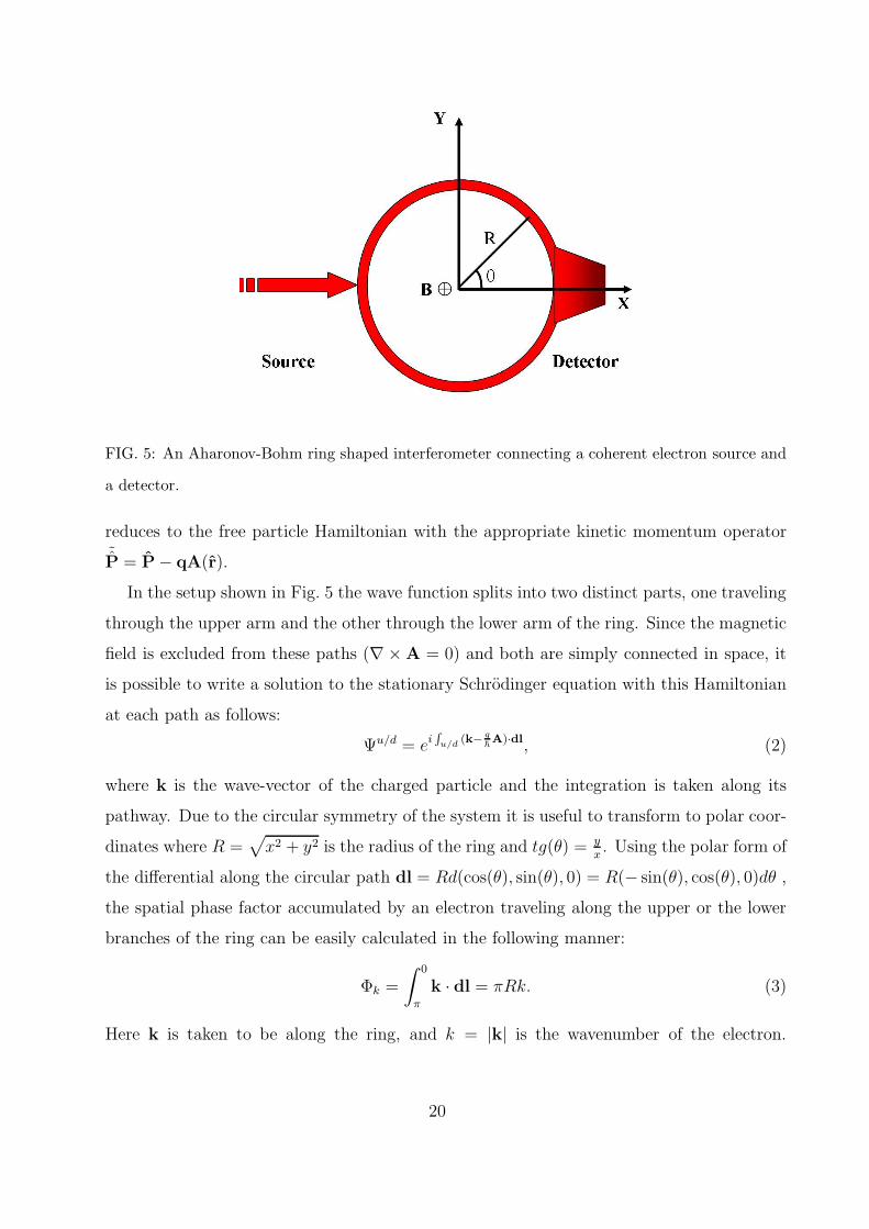
FIG. 5: An Aharonov-Bohm ring shaped interferometer connecting a coherent electron source and
a detector.
reduces to the free particle Hamiltonian with the appropriate kinetic momentum operator˜P = P− qA(r).
In the setup shown in Fig. 5 the wave function splits into two distinct parts, one traveling
through the upper arm and the other through the lower arm of the ring. Since the magnetic
field is excluded from these paths (∇× A = 0) and both are simply connected in space, it
is possible to write a solution to the stationary Schrodinger equation with this Hamiltonian
at each path as follows:
Ψu/d = eiR
u/d (k− q~A)·dl, (2)
where k is the wave-vector of the charged particle and the integration is taken along its
pathway. Due to the circular symmetry of the system it is useful to transform to polar coor-
dinates where R =√x2 + y2 is the radius of the ring and tg(θ) = y
x. Using the polar form of
the differential along the circular path dl = Rd(cos(θ), sin(θ), 0) = R(− sin(θ), cos(θ), 0)dθ ,
the spatial phase factor accumulated by an electron traveling along the upper or the lower
branches of the ring can be easily calculated in the following manner:
Φk =
∫ 0
π
k · dl = πRk. (3)
Here k is taken to be along the ring, and k = |k| is the wavenumber of the electron.
20

When a uniform∗∗ magnetic field is applied perpendicular to the cross section of the ring,
B = (0, 0, Bz), the vector potential may be written as A = −12r × B = 1
2Bz(−y, x, 0) =
RBz
2(− sin(θ), cos(θ), 0). Thus, the magnetic phase accumulated by the electron while trav-
eling from the source to the detector in a clockwise manner through the upper path is given
by:
Φum = −q
~
∫ 0
π
A · dl = πφ
φ0. (4)
Here, φ = BzS is the magnetic flux threading the ring, φ0 = hq
is the flux quantum, and
S = πR2 is the cross section area of the ring. For an electron traveling through the lower
path in a counterclockwise manner the magnetic phase has the same magnitude however an
opposite sign:
Φlm = −q
~
∫ 2π
π
A · dl = −π φφ0. (5)
The electron intensity measured at the detector is proportional to the square absolute
value of the sum of the upper and lower wave function contributions:
I ∝∣∣Ψu + Ψd
∣∣2 =
∣∣∣∣eiπ
“
Rk+ φφ0
”
+ eiπ
“
Rk− φφ0
”
∣∣∣∣2
= 2
[1 + cos
(2π
φ
φ0
)]. (6)
Thus, we find that the intensity measured at the detector is a periodic function of the
magnetic flux threading the ring’s cross section. As mentioned before, this general and
important result holds also when the magnetic field is not applied uniformly and measurable
intensity changes may be observed at the detector even if the magnetic field applied is
excluded from the circumference of the ring to which the electrons are bound.
B. Length Scales
The model described above presents an idealized system for which the charge carrying
particles travel from the source to the detector without losing either momentum or phase.
When considering the issue of measuring the AB effect in a realistic system, a delicate
∗∗ The calculation given here assumes a uniform magnetic field even-though, it was claimed that Eq. 2 holds
only in regions in space where B = 0. Nevertheless, due to the fact that the electrons are confined to
move on the one-dimensional ring, there is no essential difference between the case of a singular magnetic
field and a homogeneous magnetic field. Therefore, the usage of the phases calculated here in Eq. 6 is
valid. Furthermore, it should be noted that due to Stokes law, the line integration of A over a closed loop
will always give the magnetic flux threading the ring whether the field is uniform, singular or of any other
form.
21
balance between three important length scales is needed: 1. the Fermi electrons de-Broglie
wave length, 2. the mean free path, and 3. the coherence length scale. We shall now give
a brief description of each of these length scales and its importance in coherent transport
problems.
1. Fermi de-Broglie wave length
As in the optical double-slit experiment, the wavelength of the conducting electrons
determines the interference intensity measured at the detector. At low temperatures the net
current is carried by electrons in the vicinity of the Fermi energy and thus by controlling their
wavelength one can determine whether positive or negative interference will be measured at
the detector in the absence of a magnetic field.
In order to achieve positive interference, an integer number of Fermi wave lengths should
fit into half the circumference of the ring (Fig. 5): L = nλF . Here, n is an integer, L = πR
is half of the circumference of the ring, and λF is the Fermi electrons wavelength given by
the well know de-Broglie relation λF = hPF
= 2πkF
, where, PF is the momentum of the Fermi
electrons, and kF is the associated wavenumber.
For such a condition to be experimentally accessible, the Fermi wavelength should ap-
proximately be of the order of magnitude of the device dimensions. Too short wavelengths
will give rise to extreme sensitivity of the interference pattern on the Fermi wavenumber,
while too long wavelengths will show very low sensitivity.
We shall return to the importance of controlling the wavelength of the conducting elec-
trons in realistic systems measurements in chapters IV and VII.
2. Mean free path
An electron traveling in a perfect crystal can be viewed as a free particle with a renormal-
ized mass.131 This mass, which is usually referred to as the effective mass of the electrons in
the crystal, incorporates the net effect of the periodic nuclei array on the conducting elec-
trons. When impurities or defects exist in the crystalline structure the electrons may scatter
upon them. Such scattering implies a random change in the electron’s momentum and thus
destroys the ballistic nature of the conductance. The mean free path is the average distance
22

an electron travels before its momentum is randomized due to a collision with an impurity. If
the scattering taking place at the impurities sites is elastic, such that the electron’s energy
and the magnitude of its momentum are conserved and only the direction of the momentum
is randomized then for a given trajectory a stationary interference pattern will be observed.
However, different electron trajectories will give rise to different interference intensities and
the overall interference pattern will not be stationary and thus will be averaged to zero.
Therefore, in order to be able to observe coherent phenomena the dimension of the system
under consideration should not exceed the typical mean free path of the charge carrying
particles within it at the given temperature.
3. Coherence length scale
Inelastic scattering may occur when the impurities have internal degrees of freedom
which may exchange energy with the scattered electrons. Such scattering events alter the
phase of the conducting electron. AB interferometry requires that a constant phase difference
exists between the trajectories of electrons moving in the upper and the lower arms of the
interferometer ring. Thus, for stationary inelastic scatterers which shift the phase of the
electrons in a persistent manner, a constant interference pattern will be measured at the
detector. Although the intensity at zero magnetic field will not necessarily be at its maximal
value, AB oscillations will be observed. When the scatterers are not stationary, and the phase
shifts they induce are not correlated between the two arms of the ring, the coherent nature
of the conductance is destroyed and the AB interference pattern is wiped out. Apart from
impurities, inelastic scattering may occur due to electron-phonon processes, and electron-
electron interactions. The later conserve the total energy but allow energy exchange and
thus phase randomization.
C. The open question
As mentioned above, the design of a realistic AB interferometer requires a careful con-
sideration of the typical length scales of the conducting electrons. In order to measure
a significant AB periodicity it is necessary to reduce the dimensions of the interferome-
ter beneath the momentum and phase relaxation length scales and make it comparable to
23

the de-Broglie wave length. As an example, for a micrometer scale GaAs/AlGaAs based
two-dimensional electron gas ring the expected AB periodicity is of the order of milliTesla:
hqπR2 ≈ 1 · 10−3Tesla. However, the typical de-Broglie wave length is of the order of ∼ 30nm,
and the mean free path (momentum relaxation length scale) is three orders of magnitude
larger (∼ 30µm) while the phase relaxation length is ∼ 1µm ††. Therefore, due to momen-
tum relaxation and dephasing processes, which take place on the same scale of the ring
dimensions, the amplitude of the AB oscillations is considerably damped and any realistic
implementation is hence impractical. As a result, we are compelled to consider nanometer
sized molecular based AB interferometers. Since two molecules of the same material are, by
definition, identical defects or impurities in such devices do not exist and the only source
of phase relaxation is the exchange of energy with the vibrational degrees of freedom of
the molecule. Thus, at low enough temperatures at which such scattering is suppressed the
transport through the molecule is coherent and significant AB oscillations are expected to
be measured.
A very important advantage of miniaturizing the interferometer is that the transport can
be directed to a single, preselected energy level on the ring. Due to quantum confinement
effects the energy spacing of the levels on the ring scales as (2n+1)~2
2m?R2 where n is the quantum
number of the conducting electron, and m? is its effective mass. When the radius of the
ring is reduced from the micrometer scale into the nanometer scale, the energy spacing is
increased by six orders of magnitude for a given quantum number. Consequently, instead
of transmitting through a finite density of states which characterizes the Fermi electrons in
micrometer scale devices, it is possible to transmit through a single, well defined, energy
level on the ring. Therefore, reducing effects resulting from heterogeneous broadening and
remaining with the homogeneous broadening of the single level due to its coupling to the
leads or to the vibrational modes of the ring. In this case the conductance becomes less
sensitive to temperature effects.
Nevertheless, on top of the engineering challenge of fabricating such small and accurate
devices, another substantial physical limitation jeopardizes the whole concept. When consid-
ering a nanometer sized AB loop the period of the magnetic interference oscillations increases
†† It should be mentioned that both the mean free path and the phase relaxation length exhibit strong
temperature dependence.
24

considerably and becomes comparable to hqπR2 ≈ 1 ·103Tesla. Magnetic fields of these orders
of magnitude are, by far, not accessible experimentally and thus AB interferometry is not
expected to be measured for miniaturized circular systems.
Therefore, a question to be raised is whether electronic devices based on the AB effect
can be scaled down to the molecular/nanometric level, in which transport is expected to
be coherent, even though the full AB periodicity is achieved at irrationally high magnetic
fields?
The purpose of the next chapter is to present the basic physical principles that set the
path to overcome the above mentioned limitation and allow for the design of miniaturized
electronic devices based on the AB effect.
25

IV. CONTINUUM MODEL
In the last chapter we have introduced the concept of the AB periodicity in magnetic
interferometers of charged particles. The interference intensity was shown to be proportional
to the magnetic flux threading the circular path linking the source of coherent electron and
the detector (see Fig. 5). This periodicity, which is robust to all AB setups, is determined
solely by the charge of the conducting entities and by the dimensions of the interferometer.
It was claimed that for a nanometer scale conducting loop, the magnetic fields needed to
complete a full AB cycle are irrationally high and thus no AB interferometry is possible at
such miniaturized devices.
It is the goal of this chapter to show how this argumentation is only partially correct. Even
though it is true that the full AB cycle for nanometer sized conducting loops is accomplished
at extremely high magnetic fields, the dependence found in Eq. 6, can be modified such
that very high sensitivity of the interference intensity is achieved upon the application of
reasonably low magnetic field.
For this purpose we shall now introduce a simplified continuum model63,97–100,103,132–135
description of an AB interferometer. The model consists of a one dimensional (1D) single
mode conducting ring coupled to two 1D single mode conducting leads as depicted in Fig. 6.
The transport is considered to be ballistic along the conducting lines. Elastic scattering
occurs at the two junctions only.
FIG. 6: An illustration of a 1D coherent transport continuum model of an AB interferometer.
Even-though this model neglects important effects such as electron-electron interactions,
and electron-phonon coupling, and also disregards the detailed electronic structure of the
molecular device, and the exact leads-device junctions structure, it succeeds in capturing
the important physical parameters needed to control the profile of the AB period.
26
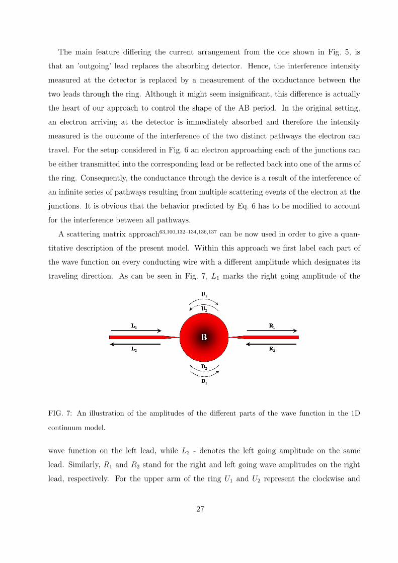
The main feature differing the current arrangement from the one shown in Fig. 5, is
that an ’outgoing’ lead replaces the absorbing detector. Hence, the interference intensity
measured at the detector is replaced by a measurement of the conductance between the
two leads through the ring. Although it might seem insignificant, this difference is actually
the heart of our approach to control the shape of the AB period. In the original setting,
an electron arriving at the detector is immediately absorbed and therefore the intensity
measured is the outcome of the interference of the two distinct pathways the electron can
travel. For the setup considered in Fig. 6 an electron approaching each of the junctions can
be either transmitted into the corresponding lead or be reflected back into one of the arms of
the ring. Consequently, the conductance through the device is a result of the interference of
an infinite series of pathways resulting from multiple scattering events of the electron at the
junctions. It is obvious that the behavior predicted by Eq. 6 has to be modified to account
for the interference between all pathways.
A scattering matrix approach63,100,132–134,136,137 can be now used in order to give a quan-
titative description of the present model. Within this approach we first label each part of
the wave function on every conducting wire with a different amplitude which designates its
traveling direction. As can be seen in Fig. 7, L1 marks the right going amplitude of the
FIG. 7: An illustration of the amplitudes of the different parts of the wave function in the 1D
continuum model.
wave function on the left lead, while L2 - denotes the left going amplitude on the same
lead. Similarly, R1 and R2 stand for the right and left going wave amplitudes on the right
lead, respectively. For the upper arm of the ring U1 and U2 represent the clockwise and
27
counterclockwise traveling amplitudes, respectively, whereas D2 and D1 are the clockwise
and counterclockwise traveling amplitudes on the lower arm.
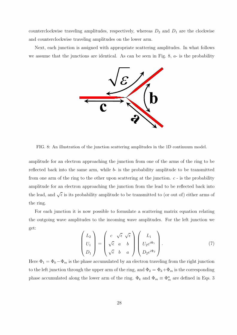
Next, each junction is assigned with appropriate scattering amplitudes. In what follows
we assume that the junctions are identical. As can be seen in Fig. 8, a- is the probability
FIG. 8: An illustration of the junction scattering amplitudes in the 1D continuum model.
amplitude for an electron approaching the junction from one of the arms of the ring to be
reflected back into the same arm, while b- is the probability amplitude to be transmitted
from one arm of the ring to the other upon scattering at the junction. c - is the probability
amplitude for an electron approaching the junction from the lead to be reflected back into
the lead, and√ε is its probability amplitude to be transmitted to (or out of) either arms of
the ring.
For each junction it is now possible to formulate a scattering matrix equation relating
the outgoing wave amplitudes to the incoming wave amplitudes. For the left junction we
get:
L2
U1
D1
=
c√ε√ε
√ε a b
√ε b a
L1
U2eiΦ1
D2eiΦ2
. (7)
Here Φ1 = Φk−Φm is the phase accumulated by an electron traveling from the right junction
to the left junction through the upper arm of the ring, and Φ2 = Φk+Φm is the corresponding
phase accumulated along the lower arm of the ring. Φk and Φm ≡ Φum are defined in Eqs. 3
28

and 4, respectively. An analogous equation can be written down for the right junction:
R1
U2
D2
=
c√ε√ε
√ε a b
√ε b a
R2
U1eiΦ2
D1eiΦ1
. (8)
In order to insure current conservation during each scattering event at the junctions one
has to enforce the scattering matrix to be unitary. This condition produces the following
relations between the junction scattering amplitudes: a = 12(1 − c), b = −1
2(1 + c), and
c =√
1 − 2ε. It can be seen that the entire effect of the elastic scattering occurring at the
junctions can be represented by a single parameter which we choose to be ε - the junction
transmittance probability.
Solving these equations ‡‡ and setting the right incoming wave amplitude R2 equal to
zero, one gets a relation between the outgoing wave amplitude R1 and the incoming wave
amplitude L1. Using this relation it is possible to calculate the transmittance probability
through the ring which is given by:138
T =
∣∣∣∣R1
L1
∣∣∣∣2
=A[1 + cos(2φm)]
1 + P cos(2φm) +Q cos2(2φm), (9)
where the coefficients are functions of the spatial phase and the junction transmittance
probability:
A = 16ε2[1−cos(2Φk)]R
P = 2(c−1)2(c+1)2−4(c2+1)(c+1)2 cos(2Φk)R
Q = (c+1)4
R
R = (c− 1)4 + 4c4 + 4 − 4(c2 + 1)(c− 1)2 cos(2Φk) + 8c2 cos(4Φk).
(10)
The numerator of Eq. 9 resembles the result obtained for the interference of two distinct
electron pathways (given by Eq. 6). The correction for the case where the electrons are not
absorbed at the detector is given by the coefficient A and the denominator expression.
Two important independent parameters contribute to the shape of the magneto-
transmittance spectrum: the junction transmittance probability - ε, and the conducting
‡‡ It is useful to initially solve the four equations involving the on-ring amplitudes U1, U2, D1, and D2 as
a function of the leads incoming amplitudes L1, and R2. Plugging the solution into the equation for the
outgoing amplitude R1 results in the desired relation between R1 and L1, needed for the transmittance
calculation.
29

electron wavenumber k appearing in the spatial phase Φk = πRk. In Fig. 9 we present the
transmittance probability (T ) through the ring as a function of the normalized magnetic
flux threading it, for a given value of the spatial phase and several junction transmittance
probabilities. It can be seen that for high values of the junction transmittance probability
0 0.2 0.4 0.6 0.8 1φ/φ0
0
0.2
0.4
0.6
0.8
1
Tra
nsm
ittan
ce p
roba
bilit
y
0 0.2 0.4 0.6 0.8 10
0.2
0.4
0.6
0.8
1
ε = 0.05ε = 0.25ε = 0.45
FIG. 9: AB transmittance probability, calculated using Eqs. 9 and 10, as a function of the magnetic
flux for different junction transmittance probabilities and kR = 0.5 . For high values of ε (dash-
dotted green line) the transmittance probability is similar to that predicted by Eq. 6. As ε is
decreased the transmittance peaks narrow (dashed red line). For very small values of ε the peaks
become δ function-like (full black line).
(dashed-dotted green line in the figure) the magneto-transmittance behavior is similar to
that predicted by Eq. 6, i.e. a cosine function. As ε is reduced from its maximal value of
12
the width of the transmittance peaks is narrowed (dashed red line and full black line).
At the limit of vanishing ε the magneto-transmittance peaks become a sharp δ function.
Physically, this can be explained based on the fact that ε controls the coupling between the
leads and the ring. High values of ε correspond to a high probability of the electron to mount
(or dismount) the ring and thus, relate to strong leads-ring coupling. At such values, the
30

lifetime of the electron on the ring is short and therefore, the energy levels characterizing the
ring are significantly broadened. The application of a magnetic field will change the position
of these energy levels, however, due to their wide nature they will stay in partial resonance
with the energy of the incoming electrons for a wide range of magnetic fields. When reduc-
ing the coupling (low values of ε) the doubly degenerate energy levels of the ring sharpen.
If we assume that at zero magnetic flux two such energy levels are in resonance with the
incoming electrons, then upon applying a finite magnetic field the degeneracy is removed
such that one level has its energy raised and the other lowered. This splitting causes both
sharp energy levels to shift out of resonance and thus reduces the transmittance probability
through the ring dramatically. The situation described above for the low coupling regime is,
in fact, resonant tunneling occurring through the slightly broadened (due to the coupling to
the leads) energy levels of a particle on a ring. Here, the free particle §§ time-independent
scattering wave function on the wires, ψk(z) = eikz , has the same form of the wave function
of a particle on a ring ψm(θ) = eimθ where m = 0,±1,±2, . . . . Upon mounting the ring,
the electron’s wave number, km, is quantized according to the following relation: Rkm = m.
The value of m for which resonant tunneling takes place is determined by the condition that
the kinetic energy of the free electron on the wire equals a sharp energy eigenvalues of the
ring139:
~2k2
2m?=
~2(m− φ
φ0)2
2m?R2. (11)
In order to achieve resonance one has to require that k = (m− φφ0
)/R. A slight change in the
magnetic flux, disrupts this resonance condition and reduces the transmittance considerably.
For different values of the wavenumber on the leads the resonance condition in Eq. 11 will
be obtained at different values of the magnetic flux.
This effect is depicted in Fig. 10 where the transmittance probability is plotted against
the normalized magnetic flux threading the ring, for a given value of ε and several spatial
phase factors. As depicted in the figure, changing the spatial phase results in a shift of the
location of the transmittance peaks along the AB period. This is analogous to the change in
the position of the intensity peaks of the interference pattern observed in the optical double-
§§ It should be emphasized that the validity of effective mass models for the description of nanometer scale
systems may be very limited and it is presented here merely to give some physical intuition of some of
the main features obtained by the continuum model.
31

0 0.2 0.4 0.6 0.8 1φ/φ0
0
0.2
0.4
0.6
0.8
1
Tra
nsm
ittan
ce p
roba
bilit
y
0 0.2 0.4 0.6 0.8 10
0.2
0.4
0.6
0.8
1
kR = 0.05kR = 0.25kR = 0.45
FIG. 10: AB transmittance probability as a function of the magnetic flux for different spatial phases
and ε = 0.25. By changing the value of kR from ∼ n (dashed-dotted green line) to ∼ n + 0.5 (Full
black line), where n is an integer, it is possible to shift the transmittance peaks from the center of
the AB period to its edges, respectively.
slit experiment when varying the wavelength of the photons. For kR values of ∼ 0, 1, 2, · · ·(dashed-dotted green line in the figure) the peaks are located near the center of the AB
period, while for values of ∼ 0.5, 1.5, 2.5, · · · the peaks are shifted toward the period’s lower
and higher edges (Full black line). In a realistic system such control can be achieved by the
application of a gate field that serves to accelerate (or decelerate) the electron as it mounts
the ring. The gate potential, Vg, thus modifies the resonance condition of Eq. 11 to:
~2k2
2m?=
~2(m− φ
φ0)2
2m?R2+ Vg. (12)
Eq. 12 implies that a change in the gate potential influences the magnetic flux at which
resonance is attained. Therefore, the transmittance resonances position along the AB period
can be varied as shown in Fig. 10.
Considering the original goal of measuring AB magneto-transmittance effects in nanome-
32

ter scale interferometers, we see that even though the full AB period is out of experimental
reach, a delicate combination of an appropriate conducting electrons wavenumber and
weak leads-ring coupling, enables to shift the transmittance peak toward the low magnetic
fields regime while at the same time dramatically increase the sensitivity to the external
magnetic field.
This important result is depicted in Fig. 11, where magnetic switching for a 1nm radius
ring is obtained at a magnetic field of ∼ 1 Tesla while the full AB period (see inset of the
figure) is achieved at magnetic fields orders of magnitude larger.
0 0.25 0.5 0.75 1Magnetic field (Tesla)
0
0.5
1
Tra
nsm
ittan
ce p
roba
bilit
y
0 500 1000 1500
0
0.5
1
FIG. 11: Low field magnetoresistance switching of a 1nm ring weakly coupled to two conducting
wires as calculated using the continuum model. The parameters chosen in this calculation are:
ε = 0.005, and kR ≈ 1. Inset showing the full AB period of ≈ 1300 Tesla.
This result resembles the change in the interference intensity measured by the optical
Mach-Zehnder interferometer upon altering the phase of the photons on one of the interfer-
ometric paths. The plausibility of applying these principles to realistic molecular systems is
the subject of chapters VI and VII. But first, an important question, which considers the
uniqueness of using magnetic fields, has to be answered.
33

V. WHY USE MAGNETIC FIELDS?
In the previous chapter we have identified the important physical parameters that have
to be taken into account when considering the utilization of nanostructures as magnetore-
sistance devices based on the AB effect. A legitimate question that may be raised at this
point is why use magnetic fields to switch the conductance, while switching devices based
on other external perturbations, such as field effect transistors (FETs), already exist and
operate even at the molecular scale140–144?
In order to address this question it is useful to consider an expansion of the two terminal
continuum model described in chapter IV to the three terminal case.145 An illustration of
the three terminal setup is given in Fig. 12
FIG. 12: An illustration of a 1D coherent transport continuum model of a three terminal AB
interferometer.
The scattering matrix approach may be used in a similar manner to that described for
the two terminal setup. An illustration of the three-terminal setup parameters designation
is given in Fig. 13. We denote (panel (a)) by α, β, and γ = 2π−α−β the angles between the
three conducting leads. Similar to the two terminal model, we label the wave amplitudes
on each ballistic conductor of the system as shown in panel (b) of Fig. 13.
34

(a) (b)
FIG. 13: Parameters designation in the three terminal continuum model. Panel a: The angular
separations between the three terminals. Panel b: The amplitudes of the different parts of the
wave function.
The scattering amplitudes characterizing the junctions are given in Fig. 8, and obey the
scattering matrix unitary condition: c =√
1 − 2ε, a = 12(1 − c), and b = −1
2(1 + c). For
simplicity, in what follows we assume that all the junctions are identical. This assumption
can be easily corrected to the case of non-identical junctions.
Using these notations it is again possible to write scattering matrix relations between the
incoming and outgoing wave amplitudes at each junction:
L2
U1
D1
=
c√ε√ε
√ε a b
√ε b a
L1
U2eiΦα
1
D2eiΦβ
2
R1
M1
U2
=
c√ε√ε
√ε a b
√ε b a
R2
M2eiΦγ
1
U1eiΦα
2
I1
D2
M2
=
c√ε√ε
√ε a b
√ε b a
I2
D1eiΦβ
1
M1eiΦγ
2
.
(13)
35

Here Φ∆=α,β,γ1 = ∆Rk−∆ φ
φ0, and Φ∆=α,β,γ
2 = ∆Rk+∆ φφ0
. Eliminating the equations for the
wave amplitudes on the ring (U1,2, D1,2,M1,2), similar to the two-terminal continuum model
treatment, and plugging the solution in the equations for the outgoing amplitudes, I1 and
R1, we get a relation between the incoming amplitude on the left lead L1 and both outgoing
amplitudes. The probability to transmit through the upper (lower) outgoing lead is given
by T u =∣∣∣R1
L1
∣∣∣2
(T l =∣∣∣ I1L1
∣∣∣2
). The exact expressions for these transmittance probabilities,
even when setting the incoming wave amplitudes R2 and I2 to zero, are somewhat tedious,
however they are given here for the sake of completeness.
The denominator of the transmittance probability for both output channels is given by
the following expression:
Tdenominator =
1
16(c2 + 1)(19 − 12c+ 2c2 − 12c3 + 19c4) + 32c3 cos(4πkr)+
2(c− 1)4ccos[4πkr(1 − 2α)] + cos[4πkr(1 − 2β)] + cos[4πkr(1 − 2γ)]−
8(c− 1)2c(c2 + 1)cos[4πkr(α− 1)] + cos[4πkr(β − 1)] + cos[4πkr(γ − 1)]−
4(c− 1)2(2 − c+ 2c2 − c3 + 2c4)[cos(4πkrα) + cos(4πkrβ) + cos(4πkrγ)]+
2(c− 1)4(c2 + 1)cos[4πkr(α− β)] + cos[4πkr(α− γ)] + cos[4πkr(β − γ)]−
0.125(c+ 1)4×
−4[1 + c(c− 1)] cos(2πkr) + (c− 1)2[cos[2πkr(1 − 2α)] + cos[2πkr(1 − 2β)]
+ cos[2πkr(1 − 2γ)]] cos(2πφ
φ0) +
1
16(c+ 1)6 cos2(2π
φ
φ0).
(14)
The numerator of the transmittance probability through the upper output channel is given
36
by:
T unumerator = −0.5ε2−4(1 + c2)+
2(c− 1)2 cos(4πkrα) + (c+ 1)2 cos(4πkrβ) + 2(c− 1)2 cos(4πkrγ)+
4c cos [4πkr(α+ γ)] − (c− 1)2 cos [4πkr(α− γ)]−
2c(c+ 1) cos
[2π
(φ
φ0− kr
)]− 2(c+ 1) cos
[2π
(φ
φ0+ kr
)]−
(c2 − 1) cos
[2π
(φ
φ0+ (1 − 2α)kr
)]+ (c2 − 1) cos
[2π
(φ
φ0− (1 − 2α)kr
)]+
2(c+ 1) cos
[2π
(φ
φ0
+ (1 − 2β)kr
)]+ 2c(c+ 1) cos
[2π
(φ
φ0
− (1 − 2β)kr
)]−
(c2 − 1) cos
[2π
(φ
φ0+ (1 − 2γ)kr
)]+ (c2 − 1) cos
[2π
(φ
φ0− (1 − 2γ)kr
)].
(15)
The numerator of the transmittance probability through the lower output channel is given
by:
T lnumerator = −0.5ε2−4(1 + c2)+
(c+ 1)2 cos(4πkrα) + 2(c− 1)2 cos(4πkrβ) + 2(c− 1)2 cos(4πkrγ)+
4c cos [4πkr(β + γ)] − (c− 1)2 cos [4πkr(β − γ)]−
2c(c+ 1) cos
[2π
(φ
φ0+ kr
)]− 2(c+ 1) cos
[2π
(φ
φ0− kr
)]+
2c(c+ 1) cos
[2π
(φ
φ0
+ (1 − 2α)kr
)]+ 2(c+ 1) cos
[2π
(φ
φ0
− (1 − 2α)kr
)]+
(c2 − 1) cos
[2π
(φ
φ0
+ (1 − 2β)kr
)]− (c2 − 1) cos
[2π
(φ
φ0
− (1 − 2β)kr
)]+
(c2 − 1) cos
[2π
(φ
φ0+ (1 − 2γ)kr
)]− (c2 − 1) cos
[2π
(φ
φ0− (1 − 2γ)kr
)].
(16)
The backscattering probability is the complementary part of the sum of the transmittance
probability through both the upper and the lower leads.
The resulting transmittance probability through one of the outgoing leads, for the sym-
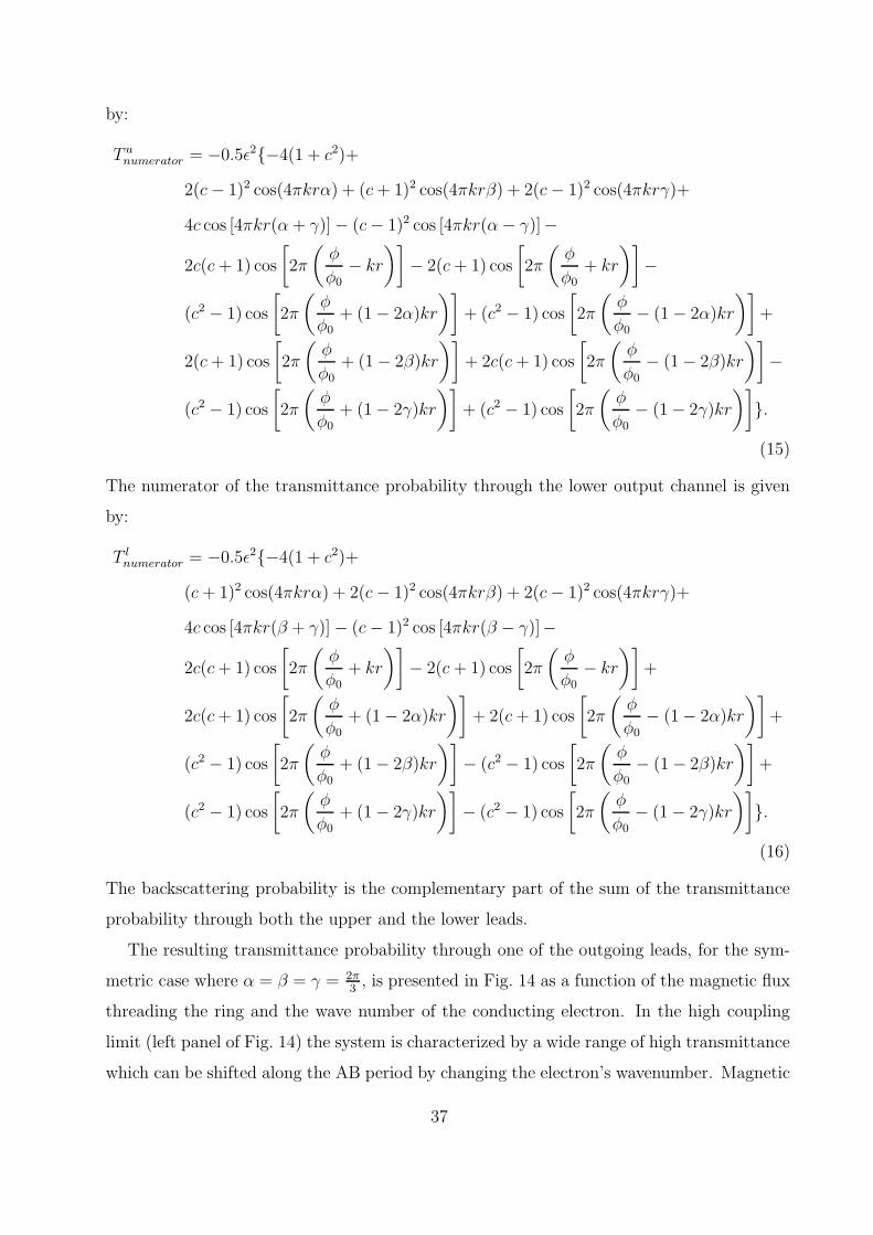
metric case where α = β = γ = 2π3
, is presented in Fig. 14 as a function of the magnetic flux
threading the ring and the wave number of the conducting electron. In the high coupling
limit (left panel of Fig. 14) the system is characterized by a wide range of high transmittance
which can be shifted along the AB period by changing the electron’s wavenumber. Magnetic
37
FIG. 14: The transmittance of a three-terminal device as a function of the magnetic flux and the
wavenumber of the conducting electron as calculated using the continuum model. Left panel: high
coupling (ε = 0.495), right panel: low coupling (ε = 0.095). Color-bar: deep blue - no transmittance
(T = 0), deep red - full transmittance (T = 1).
switching of the transmittance at a given wavenumber value for this coupling regime requires
high magnetic fields, since the transmittance peaks are quite broad.
As the coupling is decreased from its maximal value of ε = 0.5 to very low values (right
panel of Fig. 14), a resonant tunneling junction is formed and the transmittance probability
becomes very sensitive to the magnetic flux. Similar to the two terminal case, this is trans-
lated to sharper peaks that develop in the magnetotransmittance curve. For the parameters
studied in the right panel of Fig. 14 there is negligible transmittance for all values of k at
zero magnetic field. We notice that the position of the first maximum in the transmittance
depends linearly on the value of φ and k. Fine tuning the wave number to a value that sat-
isfies kR = 0.5 results in the appearance of the sharp transmittance peak at finite, relatively
low, magnetic flux and thus allows the switching of the device at feasible magnetic fields.
A careful examination of the transmittance probability spectrum for kR = 0.5 at the low
magnetic flux regime reveals that the appearance of the transmittance peak is sensitive to the
polarity of the magnetic flux. While at a positive magnetic flux a pronounce peak is observed,
at the negative magnetic flux counterpart this peak is absent. This magnetic rectification
phenomena is, allegedly, in contrast with the Onsager symmetry relation138,146–148 obeyed in
the two terminal case which states that g(φ) = g(−φ) where g is the conductance.
38

This contradiction is resolved by considering the transmittance probability through the
other output channel which can be obtained by applying a reflection transformation with
respect to a plain passing through the incoming lead and perpendicular to the cross section
of the ring. The Hamiltonian of the system is invariant to such a transformation only
if accompanied by a reversal of the direction of the magnetic field. It follows that the
transmittance probability through one outgoing lead is the mirror image of the transmittance
through the other. Thus, we find that for the second output channel (not shown) the peak
is observed at a negative magnetic flux rather than at a positive one. Onsager’s condition
is, therefore, regained for the sum of the transmittance probabilities through both output
channels.
The above analysis implies that at zero magnetic field both output channels are closed
and the electron is totally reflected. The application of a relatively small positive magnetic
field opens only one output channel and forces the electrons to transverse the ring through
this channel alone. Reversing the polarity of the magnetic field causes the output channels
to interchange roles and forces the electrons to pass the ring through the other lead.
To summarize this section, magnetic fields offer unique controllability over the conduc-
tance of nanometer scale interferometers. Their polarity can be used to selectively switch
different conducting channels. While non-uniform scalar potentials have been used in meso-
scopic physics to obtain a similar effect,149 such control cannot be obtained via the ap-
plication of uniform scalar potentials which are commonly used to control molecular scale
devices. This is due to the fact that such scalar potentials lack the symmetry breaking
nature of magnetic vector potentials.
The question now shifts to the plausibility of the principles discussed above within the
framework of the continuum model in molecular based devices. In order to address this
question we present, in the following chapter, a magnetic extended Huckel theory developed
for the atomistic calculation of the magnetoresistance of molecular systems.
39

VI. ATOMISTIC CALCULATIONS - MODEL
The model presented in chapter IV is a one-dimensional single mode transport model
which was introduced in order to identify and isolate the important physical parameters
that allow the control over the profile of the AB period. In order to capture the more
complex nature of the electronic structure of realistic nanoscale AB interferometers and its
influence on the AB magnetoresistance measurement we now present a model which was
developed for the calculation of magneto-conductance through molecular setups. Within
our approach we calculate the conductance using non-equilibrium Green’s function (NEGF)
formalism. In the case of pure elastic scattering, this reduces to the Landauer formalism,
which relates the conductance to the transmittance probability through the system. The
transmittance is calculated using Green’s functions (GFs) and absorbing potentials tech-
niques, based on the electronic structure of the system. The electronic structure is, in turn,
calculated using an extension of the extended Huckel method which incorporates the influ-
ence of external magnetic fields. The resulting magneto-conductance spectrum can be then
studied for different molecular setups and conditions.
A. Conductance
We are interested in calculating the conductance through a molecular device coupled to
two macroscopic conducting leads in the presence of an external magnetic field. Our starting
point is the current formula obtained within the NEGF framework:63,150
IL(R) =2e
~
∫dE
2πTr
[Σ<
L(R)(E)G>d (E) − Σ>
L(R)G<d (E)
]. (17)
Here IL(R) is the net current measured at the left (right) molecule-lead junction, G<d (E)
and G>D(E) are the lesser and greater device Green’s functions, respectively, and Σ<
L(R) and
Σ>L(R) are the left (right) lesser and greater self energy terms respectively. The first term
in the trace in Eq. 17 can be identified with the rate of in-scattering of electrons into the
device from the left (right) lead. Similarly the second term represents the out-scattering
rate of electrons into the left (right) lead. The difference between these two terms gives the
net, energy dependent, flow rate of electrons through the device. When integrated over the
energy and multiplied by twice (to account for spin states) the electrons charge this results in
the net current flowing through the left (right) junction. It can be shown151 that IL = −IR
40
in analogy to Kirchoff’s law, and therefore Eq. 17 represents the full current through the
device.
The lesser and greater GFs appearing in Eq. 17 are related to the retarded (Gr(E)) and
advanced (Ga(E)) GFs, which will be discussed later, through the Keldysh equation152:G<
d (E) = Grd(E)Σ<(E)Ga
d(E)
G>d (E) = Gr
d(E)Σ>(E)Gad(E),
(18)
where in the pure elastic scattering case:
Σ< = Σ<L + Σ<
R
Σ> = Σ>L + Σ>
R.(19)
Furthermore, the lesser and greater self energy terms in Eqs. 17 and 19 are related to
the retarded (ΣrL(R)(E)) and advanced (Σa
L(R)(E)) self energies, which will also be discussed
later, in the following manner:
Σ<L(R)(E) = −fL(R)(E, µL(R))
[Σr
L(R)(E) − ΣaL(R)(E)
]
Σ>L(R)(E) =
[1 − fL(R)(E, µL(R))
] [Σr
L(R)(E) − ΣaL(R)(E)
],
(20)
where fL(R)(E, µL(R)) =[1 + eβ(E−µL(R))
]−1is the Fermi-Dirac occupation distribution in the
left (right) lead, µL(R) is the chemical potential of the left (right) lead and β = 1kBT
where
kB is Boltzmann’s constant and T is the temperature.
Upon plugging Eqs. 18 and 20 into Eq. 17, we get the following result for the current:
I =2e
~
∫dE
2π[fR(E, µR) − fL(E, µL)]
Tr [ΣrL(E) − Σa
L(E)]Grd(E) [Σr
R(E) − ΣaR(E)]Ga
d(E) .(21)
We can now define the level width matrix ΓL(R) in the following manner:
ΓL(R)(E) ≡ i[Σr
L(R)(E) − ΣaL(R)(E)
](22)
and rewrite Eq. 21 as:
I =2e
~
∫dE
2π[fL(E, µL) − fR(E, µR)]Tr [ΓL(E)Gr
d(E)ΓR(E)Gad(E)] . (23)
It is now possible to identify T (E) = Tr [ΓL(E)Grd(E)ΓR(E)Ga
d(E)] as the electron trans-
mission probability through the molecule and the difference in the Fermi-Dirac distribution
41

functions as the net, energy dependent, density of current carrying particles from the left
(right) lead to the right (left) lead, due to the difference in their chemical potentials.153
Therefore, integrating over the energy we obtain the current.
Since we are interested in calculating the conductance (g) we can now define the differ-
ential conductance as the derivative of the current with respect to the applied bias voltage
(Vb):
g =∂I
∂Vb
=2e
~
∂
∂Vb
∫dE
2π[fL(E, µL) − fR(E, µR)]Tr [ΓL(E)Gr
d(E)ΓR(E)Gad(E)] .
(24)
If one assumes that the bias voltage applied does not alter considerably the energetic struc-
ture of the device, the only contribution of the bias in Eq. 23 appears in the Fermi-Dirac
distribution functions. In what follows, this assumption is reasonable since we shall con-
sider the limit of zero bias conductance. Therefore, it is possible to directly conduct the
differentiation in equation 24 to get the following relation:
g =∂I
∂Vb
=2e
~
∫dE
2π
∂ [fL(E, µL) − fR(E, µR)]
∂VbTr [ΓL(E)Gr
d(E)ΓR(E)Gad(E)] .
(25)
If we further assume that the bias potential drops sharply and equally at both junctions154,
the chemical potentials are given by µL(R) = EL(R)f + (−)1
2eVb, where E
L(R)f is the Fermi
energy of the left(right) lead. Thus, the derivative with respect to the bias voltage appearing
in Eq. 25 is given by ¶¶ :
∂ [fL(E, µL) − fR(E, µR)]
∂Vb
= 0.5eβ
e−β|E−µL|
[1 + e−β|E−µL|]2 +
e−β|E−µR|
[1 + e−β|E−µR|]2
. (26)
If both Fermi energies of the leads are aligned with the Fermi energy of the device ∗∗∗, and
the chemical potential difference arises from the bias voltage alone, then at the limit of zero
¶¶ Since the left(right) term in Eq. 26 is symmetric with respect to µL(R) we can consider only the absolute
value |E − µL(R)| in these expressions which is beneficial when evaluating this expression numerically.
Furthermore, due to the structure of the integral in Eq. 24 it is sufficient to conduct the integration
over two narrow regions centered about µL and µR. The width of these integration windows can be
determined from the temperature and the desired integration convergence accuracy by W = log(r−1)β
,
where W is the integration window width and r is the reduction factor defined as the ratio of the value
of ∂[fL(E,µL)−fR(E,µR)]∂Vb
at µL(R) and at the edges of the integration region µL(R) ± W .∗∗∗ Experimentally this can be achieved by using identical leads and properly gating the device.
42

temperature and zero bias conductance the expression appearing in Eq. 26 approaches a
sharp δ function located at the Fermi energy of the molecule and Eq. 24, in turn, reduces
to the well established Landauer formula56,63 which directly relates the conductance to the
transmittance probability of the current carrying entity through the relevant device:
g = g0T, (27)
where g0 = 2e2
his the conductance quantum.
Considering the full expression given by Eq. 25 it can be seen that for the calculation
of the conductance, or more specifically of the transmittance probability, it is necessary to
obtain the retarded and advanced GFs of the device and the retarded and advanced self
energies of the leads. Obtaining these is the subject of the next section.
B. Retarded and advanced Green’s functions and self energies
In the previous section we have derived a formula for the conductance through a micro-
scopic device coupled to two macroscopic conducting leads based on NEGF formalism. The
purpose of this section is to obtain direct expressions for the retarded and advanced GFs
and for the retarded and advanced leads self energies that appear in this formula.
Following again the lines of Non-Equilibrium Green’s function theory155 the GF associated
with a Hamiltonian H evaluated in a non-orthogonal basis set must satisfy the following
relation in energy space:
(ES − H)G(E) = I , (28)
where E is the energy, S is the overlap matrix, G(E) is the GF, and I a unit matrix of the
appropriate dimensions.
As suggested above, in molecular conductance calculations it is customary to divide the
system into the ’device’ which is the conducting molecule† † † and the ’leads’ which are the
macroscopic conducting contacts through which electrons are injected into and taken out of
the ’device’. In a two terminal setup this is translated to the following sub-matrices devision
† † † usually one defines an ’extended molecule’ which is the molecule itself accompanied with a limited portion
of the leads which is influenced by the proximity to the molecule.
43

of Eq. 28:155,156
εSL − HL εSLd − VLd 0
εSdL − VdL εSd − Hd εSdR − VdR
0 εSRd − VRd εSR − HR
GrL(ε) Gr
Ld(ε) GrLR(ε)
GrdL(ε) Gr
d(ε) GrdR(ε)
GrRL(ε) Gr
Rd(ε) GrR(ε)
=
IL 0 0
0 Id 0
0 0 IR
.
(29)
Here, HL(R), and Hd are the left(right) semi-infinite lead, and the device Hamiltonians,
respectively, SL(R), and Sd are the left(right) lead, and the device overlap matrices, respec-
tively, VL(R)d are the coupling matrices between the left(right) lead and the device, and SL(R)d
are the overlap matrices between the left(right) lead and the device. Since the Hamiltonian
is Hermitian one finds that VdL(R) = V †L(R)d, and in the complex GISTO basis set the same
requirement applies for the overlap matrices SdL(R) = S†L(R)d. All the terms discussed above
are calculated using a formalism which will be presented in section VID.
A complex energy ε = limη→0
E + iη has to be introduce in order to shift the poles of the
Green’s function from the real axis and allow for the convergence of both an analytical and
a numerical evaluation of the integrals over the GFs. This softens the sharp singularities of
the GF into a smother Lorentzian shape which in the limit of η → 0 restores the δ function
characteristics of the imaginary part. The superscript r which stands for ’retarded’ is added
to the GFs when using this form of complex energy. It should be noted that in Eq. 29 we
assume that the leads do not directly interact so that SLR = SRL = VLR = VRL = 0.
Solving Eq. 29 for the middle column of the GF matrix results in the following expression
for the retarded device GF (which appears in Eq. 25) Grd(ε), when coupled to the two leads:
Grd(ε) =
[(Gr0
d (ε))−1 − Σr
L(ε) − ΣrR(ε)
]−1
, (30)
where Gr0d (ε) =
[εSd − Hd
]−1
is the GF of the bare device, and ΣrL(R)(ε) is the retarded self
energy of the left(right) lead given by:
ΣrL(R)(ε) =
(εSdL(R) − HdL(R)
)Gr0
L(R)(ε)(εSL(R)d − HL(R)d
). (31)
Here, Gr0L(R)(ε) =
[εSL(R) − HL(R)
]−1
is the retarded GF of the bare left(right) lead. The
advanced device GF is the Hermitian conjugate of its retarded counterpart Gad(ε) =
[Gr
d(ε)]†
.
The self energy terms appearing in Eqs. 30 and 31 represent the effect of the coupling to
the leads on the GF of the device. The calculation of these terms requires the GF of the bare
44

lead Gr0L(R)(ε). This is not a simple task since the leads are macroscopic sources of electrons
whose GFs are impossible to calculate directly. A way to overcome this obstacle is to repre-
sent the leads as periodic bulk structures of a semi-infinite nature. Using common solid state
physics techniques the periodicity of the bulk can considerably reduce the dimensionality of
the problem and thus enable the calculation of the electronic structure of the leads. For this
we use an efficient iterative procedure developed by Lopez Sancho et al.157–159 Within this
approach the semi-infinite bulk is divided into a set of identical principal layers, as shown
in Fig. 15, in such a manner that only adjacent layers overlap and interact. Using Eq. 28
EE
FIG. 15: Division of the semi-infinite bulk lead into a set of nearest neighbors interacting layers.
the resulting GF can be represented as the inverse of a nearest neighbors block-tridiagonal
matrix of the form:
G00(ε) G01(ε) G02(ε) G03(ε) · · ·G10(ε) G11(ε) G12(ε) G13(ε) · · ·G20(ε) G21(ε) G22(ε) G23(ε) · · ·G30(ε) G31(ε) G32(ε) G33(ε) · · ·
......
......
. . .
=
εS00 − H00 εS01 − V01 0 0 · · ·εS10 − V10 εS00 − H00 εS01 − V01 0 · · ·
0 εS10 − V10 εS00 − H00 εS01 − V01 · · ·0 0 εS10 − V10 εS00 − H00 · · ·...
......
.... . .
−1
.
(32)
Here, SI,I = SII,II = SIII,III = · · · ≡ S00 is the overlap matrix of the principal layer with
itself, SI,II = SII,III = SIII,IV = · · · ≡ S01 is the overlap matrix between two adjacent
layers, and as before S10 =[S01
]†. HI,I = HII,II = HIII,III = · · · ≡ H00 is the Hamiltonian
matrix of the principal layer, VI,II = VII,III = VIII,IV = · · · ≡ V01 is the coupling matrix
between two adjacent layers, and V10 =[V01
]†.
Eq. 32 is a matrix representation of a set of equations for the semi-infinite bulk GF matrix
45

elements Gij(ε) which can be solved iteratively to get a compact expression:
G(ε) =[(εS00 − H00) + (εS01 − H01)T (ε) + (εS†
01 − H†01)T (ε)
]−1
. (33)
The transfer matrices T and T are given by converging series of the form:
T (ε) = t0 + t0t1 + t0t1t2 + · · ·+ t0t1t2 · · · tn
T (ε) = t0 + t0t1 + t0t1t2 + · · ·+ t0t1t2 · · · tn,(34)
where ti and ti are defined by the recursion relations:
ti =
(I − ti−1ti−1 − ti−1ti−1
)−1t2i−1
ti =(I − ti−1ti−1 − ti−1ti−1
)−1t2i−1,
(35)
with the following initial conditions:
t0 =
(εS00 − H00
)−1
V †01
t0 =(εS00 − H00
)−1
V01.(36)
After calculating the semi-infinite bulk GF given in Eq. 33, the left and right leads self en-
ergies can be determined using Eq. 31, and the ΓL(R) matrices appearing in the conductance
expression (Eq. 25) can be calculated using Eq. 22 with, ΣaL(R)(ε) =
[Σr
L(R)(ε)]†
.
In some calculations it is found to be useful to neglect the energy dependence of the
ΓL and ΓR matrices and replace them with constant matrices. These constant matrices
elements are taken to be the elements of the energy dependent matrices evaluated at the
relevant lead chemical potential. This approximation is usually referred to as the wide band
approximation (WBA) or alternatively the wide band limit (WBL).150 At the zero bias
limit as the temperature reduces this approximation becomes valid since the integration in
Eq. 25 involves only a narrow energy window at which the Γ matrices can be approximately
regarded as constant.
C. An alternative - Absorbing imaginary potentials
A second methodology for the calculation of the transmittance probability involves the
application of absorbing potentials160,161. Within this approach the ΓL(R) matrix appearing
46

in Eq. 25 is a negative imaginary potential placed deep within the left(right) lead. The pur-
pose of this potential is to absorb an electron traveling in the lead away from the molecular
device before it reaches the ’edge’ of the lead. This assures that the effect of reflections from
the distant lead edge is suppressed to a desired accuracy and thus enables to truncate the
lead representation to a computable size.
In the present work we have used a Gaussian imaginary potential of the form VL(R) =
V0e− (z−z
L(R)0
)2
2σ2 , here V0 is the potential hight, σ the potential width, and zL(R)0 its location
along the left(right) lead assuming that the leads are located along the Z axis. The gener-
alization of the above expression to the case of arbitrary leads direction is straightforward.
The parameters of the potential are chosen such that electrons possessing a kinetic energy
in a wide band around the Fermi energy are effectively absorbed58. As a rule of thumb one
can choose the potential hight to be the location of the Fermi energy, EF , above the bottom
of the calculated valence band, E0, V0 ≈ EF − E0. The width of the potential should be
sufficiently larger than the Fermi wave length, as an example for a carbon wire we choose
σ ≈ 20a0 where a0 is Bohr’s radius. The origin of the potential zL(R)0 is chosen such that the
region of the lead close to the device where the effect of the potential is negligible contains
at least a few Fermi wave length such that the metallic nature of the lead is appropriately
captured. This choice of parameters should serve as an initial try and a convergence check
should then be conducted. The Gaussian absorbing potential is of course not a unique choice
and other forms of absorbing potential expressions can be used162.
Within the absorbing potentials methodology the system is not divided into sub-units
and the dimensionality of all the matrices appearing in Eq. 25 is the dimensionality of the
full system (device+truncated leads). The ΓL(R) matrix elements are calculated (usually
numerically) as integrals of the atomic basis functions over the imaginary potential VL(R).
It should be noted that similar to the WBA discussed above, the Γ matrices in the current
methodology are energy independent. This fact considerably reduces the computational
efforts involved in the evaluation of the transmission probability.
The device GF in Eq. 25 is now replaced by the GF of the whole system which, similar
to Eq. 30, is given by:
Gr(E) =[ES − H − iΓL − iΓR
]−1
, (37)
where S and H are the overlap and Hamiltonian matrices, respectively, calculated for the
47

whole system, and E is the real energy. The advanced GF is as before the Hermitian
conjugate of the retarded counterpart Ga(E) = [Gr(E)]†.
The last remaining task for the calculation of the conductance is the calculation of the
Hamiltonian, overlap, and coupling matrices appearing in Eq. 29. This calculation is ex-
plained in the next section.
D. Electronic structure - Magnetic Extended Huckel Theory
Our final task in the calculation of the conductance is the appropriate representation of
the electronic structure of the system under the influence of the external magnetic field. For
this purpose, a magnetic extended Huckel theory (MEHT) was developed.
We consider the Hamiltonian of the multi electronic problem, which is given by:
H =1
2me
[P − qA
]2
+ V (r). (38)
This is similar to the Hamiltonian presented in Eq. 1 apart from the fact that P and r
are vectors in the multi-electron space. Within the MEHT formalism the contribution at
zero vector potential H(A = 0) = P2
2m+ V(r) is represented by the Extended Huckel (EH)
Hamiltonian163 HEH which treats the complex many body problem using a mean field,
single-particle, semi-empirical approach. The effect of applying a vector potential is taken
into account by simply adding the appropriate magnetic terms to the EH Hamiltonian:
H = HEH − q
2me
(P · A + A · P
)+
q2
2mA2. (39)
As before we assume that the magnetic field is uniform and constant B = (Bx, By, Bz) and
thus write down the related vector potential as: A = −12r × B = −1
2(yBz − zBy, zBx −
xBz, xBy − yBx). Putting this expression in Eq. 39 we get the following electronic Hamilto-
nian164:
H = HEH − µB
~L · B +
q2B2
8me
r2⊥. (40)
Here, µB = q~
2meis the Bohr magneton, r2
⊥ = r2 − (r·B)2
B2 is the projection of r = (x, y, z)
onto the plane perpendicular to B, and L = r × P is the angular momentum operator. In
should be noted that by using this Hamiltonian we neglect effects such as Zeeman splitting
and spin-orbit coupling which relate to the spin state of the electron.
48
For the sake of simplicity, and without limiting the generality of the solution, we assume
that the AB ring is placed in the Y −Z plane and that the magnetic field is applied parallel
to the X-axis. With this the Hamiltonian in Eq. 40 is reduced to:
H = HEH + iµBBx
(y∂
∂z− z
∂
∂y
)+q2B2
x
8me(y2 + z2). (41)
A Slater Type Orbitals165,166 (STO) basis set is used to evaluate the Hamiltonian and
overlap matrices. In the presence of a magnetic field it is necessary to multiply each STO by
an appropriate gauge factor which compensates for the finite size of the set. The resulting
atomic orbitals are customarily referred to as Gauge Invariant167,168 Slater Type Orbitals
(GISTOs) and are given by:
|n, l,m >α= eiq~Aα·r|n, l,m >α= e
iqBx2~
(yαz−zαy)|n, l,m >α . (42)
Here |n, l,m >α is a STO (see Eq. A1 of appendix A) characterized by the set of quantum
numbers (n, l,m), and centered on the atomic site α. Aα is the value of the vector potential
A at the nuclear position Rα = (xα, yα, zα), and |n, l,m >α is the GISTO situated at α.
The generalized eigenvalue problem Hψn = EnSψ is solved to get the electronic energy
levels (En) and the molecular orbitals (ψn) characterizing the system. Here, H and S are the
Hamiltonian and overlap matrices with elements given by S1α,2β =α
⟨n1, l1, m1|n2, l2, m2
⟩β
and H1α,2β =α
⟨n1, l1, m1|H|n2, l2, m2
⟩β. We use the London approximation167,168 for calcu-
lating the different matrix elements. Within this approximation the gauge phase appearing
in Eq. 42 is taken outside the integral, replacing r by 12(Rα +Rβ). The overlap integrals are
then given by:
S1α,2β ≈ S1α,2βeiLαβ . (43)
Here, S1α,2β =α 〈n1, l1, m1|n2, l2, m2〉β , and Lαβ = q2~
(Aβ − Aα) · (Rα + Rβ) = qBx
2~(zαyβ −
yαzβ). The Hamiltonian matrix elements are approximated as:
H1α,2β ≈ 1
2
[H1α,2βe
iLαβ + H1β,2αeiLβα
], (44)
where H1α,2β =α
⟨n1, l1, m1|H|n2, l2, m2
⟩β. This form guarantees that the Hamiltonian
matrix remains Hermitian under the approximation.
All matrix elements in the formulation presented above are calculated analytically. The
EH Hamiltonian diagonal matrix elements are set to be equal to the ionization potentials
49

of the appropriate atomic orbital, HEH1α,1α = I.P.1α, while the off-diagonal elements are given
by an average of the corresponding diagonal elements: HEH1α,2β = k
HEH1α,1α+HEH
2β,2β
2S1α,2β, where,
k = 1.75 is a parameter chosen to give best fit to experimental data. The overlap matrix
is calculated analytically for every set of quantum numbers using a method developed by
Guseinov et al169–173 which is described in appendix A. The matrix elements of the magnetic
terms appearing in the Hamiltonian can then be expressed as linear combination of overlap
integrals and are thus also calculated without the need to perform numerical integration. The
expansion of the magnetic integrals in terms of corresponding overlap integrals is presented,
in details, in appendix B.
Before continuing, it should be mentioned that while the current model does take into
account the explicit geometry of the system and also some of the details of the system’s
electronic structure, it remains an effective one-particle model and neglects contributions
from electron-electron correlations and coupling to the vibrational degrees of freedom of the
molecular device. Furthermore, since the bias potential is assumed to drop sharply at the
leads-device junctions and its effect of the energy levels of the device is neglected, the current
model is valid only at the low bias regime.
Despite these limitations, the atomistic model presented above can serve as a first-order
approximation and reveal some important physical considerations regarding the study of the
AB effect at the nanometer scale. In the next chapter we present the magneto-resistance
behavior of several studied systems obtained using this formalism.
50

VII. ATOMISTIC CALCULATIONS - RESULTS
Using the MEHT formalism developed in chapter VI we calculate the conductance of
several characteristic atomic and molecular setups that are suggested as promising building
blocks for future nanometric magnetoresistance devices based on the AB effect. In the
present chapter we present a study the magnetoresistance behavior of these structures as a
function of the relevant physical control parameters identified in chapter IV and compare
our results to those obtained using the continuum model.
A. Atomic corral
In 1993 a group from IBM was able to confine copper surface electrons to artificially
created structures composed of individual iron atoms manipulated on the surface using
a STM tip.16 One of the most intriguing confining structures was that of a perfect ring
shaped corral created by the exact positioning of 48 iron atoms on the appropriate sites
of the copper(111) surface (See Fig. 1). Using such structures they were able to study the
stationary surface electron wave patterns arising due to the confinement, and fascinating
phenomena such as the quantum Kondo mirage effect17 were discovered. In the present
study we suggest the utilization of such an atomic corral setup as a nanometer scale AB
interferometer.
We consider a corral composed of monovalent atoms placed on a semi-conductor sur-
face and coupled to two atomic wires. The whole setup is then placed in a perpendicular
homogeneous and constant magnetic field and the conductance between the atomic wire
leads through the corral is measured, at the limit of zero bias voltage, as a function of the
threading magnetic field. Realizing that the corral itself is also constructed of an atomic
wire it is important that we first understand some basic properties of such one-dimensional
entities.
Since each atomic site contributes a single valent electron, the number of atoms in the
chain, N , must be even to get a closed shell wire. The Fermi energy of the wire has a
principal quantum number of N2
which is also the number of nodes the Fermi electrons wave
functions have. If the distance between the atomic sites, d, is constant then the separation
between the nodes is given by NdN/2
= 2d and thus the Fermi wavelength is λF = 2×2d = 4d.
51

We therefore see that for any regular atomic wire composed of monovalent atomic sites the
conducting electrons wave length is of the order of four inter atomic distances.
This simple conjecture allows us to divide the symmetric atomic corrals into two pro-
totypes: those having N = 4n and those having N = 4n + 2 atoms on the circumference,
where n is an integer number. For a N = 4n atomic corral the quantum number of the
Fermi wave function of a particle on a ring is an integer: mF = kF r = 2πλF
Nd2π
= Nd4d
= N4
= n,
and therefore the resonance condition in Eq. 11 is obtained when the magnetic field is off.
However, when N = 4n + 2, we obtain mF = n + 12
and resonance is achieved only when
φφ0
= l2
where l = ±1,±2, · · · .A similar picture arises when plotting the wave functions of the Fermi electrons. The
complex normalized wave functions of a particle on a ring are given by: Ψ±m(θ) = 1√2πe±imθ.
A linear combination of each doubly degenerate functions having the same quantum number
m results in real wave functions of the form 1√π
cos(mθ) and 1√π
sin(mθ). The cosine functions
are plotted in Fig. 16 for the two corral prototypes having m = mF = N4. As can be seen,
(a) (b)
FIG. 16: An illustration of the Fermi cosine wave functions of a particle on a ring shaped corral.
Panel a: A 4n ring with n = 5 creates a stationary solution. Panel b: A 4n + 2 ring with the same
n as before creates a destructive interference between the clockwise (blue) and counterclockwise
(red) electron pathways.
for the 4n prototype a standing wave is obtained for which both input and output leads
are located at non-stationary points. For the 4n + 2 corral at zero magnetic flux the wave
function is not stationary and the output lead is located exactly at a node of the interference
52

between the clockwise and counter clockwise traveling electrons‡ ‡ ‡.
An alternative explanation for this class devision can be given based upon the energetic
structure of the ring. Due to the symmetry of the ring, apart from the lowest energy level,
all energy levels of a particle on an uncoupled ring are doubly degenerate. This is illustrated
in Fig. 17. When considering a single valent electron per site corral the occupation of the
m = 0
m = ±1
m = ±2
m = ±3
FIG. 17: Energy level scheme of a particle on a ring
energy levels of the 4n prototype differs from that of the 4n+2 prototype. This can be seen
4n prototype 4n + 2 prototype
FIG. 18: The occupation of the energy levels of the corral for the 4n prototype (left panel) and for
the 4n + 2 prototype (right panel).
in Fig. 18 where the highest occupied molecular orbital (HOMO) occupation is presented
for both prototypes. As can be seen in the left panel of the figure, the HOMO occupation of
the 4n prototype involves two vacancies and thus is suitable for electron conduction when
‡ ‡ ‡ In fact, the interference is destructive not only at the nodes but for every point on the ring and thus this
energy level does not exist.
53

brought to resonance with the leads. While the HOMO occupation of the 4n+ 2 prototype
(right panel of Fig. 18) is full and therefore does not conduct electrons.
It is interesting to note that the sine function, which is shifted by π2
from the cosine
counterpart, has both leads located at its nodes as can be seen in Fig. 19. Therefore, at a
given leads location and in the absence of a gate potential and a magnetic field only one of
the two degenerate energy levels will conduct and the maximum zero bias conductance will
be the quantum conductance, g0.
FIG. 19: An illustration of the Fermi sine wave functions of a particle on a ring shaped corral
having N = 4n atoms with n = 5. Note that the leads are located on the wave function nodes.
This may also be explained by using energy scheme considerations. As mentioned above
the HOMO occupation of the 4n prototype has two vacancies (one for each spin) and there-
fore allows only for a single conductance quantum per spin.
After realizing these important features of one-dimensional monovalent atomic wires,
we may turn to study atomistic calculations results obtained using the imaginary potentials
method within the MEHT formalism as discussed above. In Fig. 20 the conductance through
atomic corrals composed of 40 and a 42 copper atoms is plotted60. All atoms on the corral are
separated by a distance of 2.35A. The effect of a gate potential was simulated by changing
the corral atomic orbital energies by Vg. As discussed above, at zero gate voltage the
conductance peak for the n = 40 corral is located at the low magnetic field region while for
the n = 42 corral it is located near the middle of the AB period. Two common features are
clearly observed for the two corral prototypes: (a) a large magnetic field (∼ 500−600 Tesla)
is required to complete a full AB period. (b) The conductance peaks (red spots) shift with
54

FIG. 20: Conductance as a function of the magnetic field and the gate voltage for a 40 (left panel)
and a 42 (right panel) atomic corral composed of copper atoms at T = 1K. Color code: Red -
g = g0, purple - g = 0.
the gate voltage, Vg. The latter effect is analogous to the shift of peaks seen in Fig. 10
for the continuum model as the conducting electron wave number is varied. Therefore, the
application of a gate voltage allows the control over the location of the peak conductance.
In particular, it can be used to shift the maximal conductance to zero magnetic field for the
N = 4n + 2 corral prototype and to fine tune the location of the N = 4n peak if slightly
shifted from the magnetic field axis origin.
The next step is to control the width of the conductance resonances as a function of
the magnetic field. In the continuum model, this was done by reducing the transmission
amplitude, ε. In the molecular system this can be achieved by increasing the distance
between the ring and the edge lead atom closest to the ring. Alternatively, one can introduce
an impurity atom at the junctions between the lead and the ring. However, for quantum
corrals the former approach seems more realistic.
In Fig. 21 the conductance as a function of the magnetic field is depicted for several
values of the leads-ring separation. For each generic corral prototype, a proper gate voltage
is applied to ensure maximal conductance at B = 0 Tesla. As the lead-ring separation is
increased, the lifetime of the energy levels on the ring is increased. This is translated to
a sharpening of the switching response to the magnetic field in the magneto-conductance
55
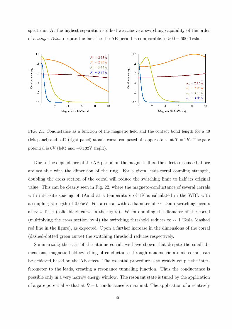
spectrum. At the highest separation studied we achieve a switching capability of the order
of a single Tesla, despite the fact the the AB period is comparable to 500 − 600 Tesla.
FIG. 21: Conductance as a function of the magnetic field and the contact bond length for a 40
(left panel) and a 42 (right panel) atomic corral composed of copper atoms at T = 1K. The gate
potential is 0V (left) and −0.132V (right).
Due to the dependence of the AB period on the magnetic flux, the effects discussed above
are scalable with the dimension of the ring. For a given leads-corral coupling strength,
doubling the cross section of the corral will reduce the switching limit to half its original
value. This can be clearly seen in Fig. 22, where the magneto-conductance of several corrals
with inter-site spacing of 1Aand at a temperature of 1K is calculated in the WBL with
a coupling strength of 0.05eV. For a corral with a diameter of ∼ 1.3nm switching occurs
at ∼ 4 Tesla (solid black curve in the figure). When doubling the diameter of the corral
(multiplying the cross section by 4) the switching threshold reduces to ∼ 1 Tesla (dashed
red line in the figure), as expected. Upon a further increase in the dimensions of the corral
(dashed-dotted green curve) the switching threshold reduces respectively.
Summarizing the case of the atomic corral, we have shown that despite the small di-
mensions, magnetic field switching of conductance through nanometric atomic corrals can
be achieved based on the AB effect. The essential procedure is to weakly couple the inter-
ferometer to the leads, creating a resonance tunneling junction. Thus the conductance is
possible only in a very narrow energy window. The resonant state is tuned by the application
of a gate potential so that at B = 0 conductance is maximal. The application of a relatively
56

0 1 2 3 4 5Magnetic field (Tesla)
0
0.2
0.4
0.6
0.8
1C
ondu
ctan
ce (
g/g 0) r=~6.4Å
r=~12.7År=~25.5Å
FIG. 22: Magneto-conductance through an atomic corral as a function of the corral dimensions.
As the diameter of the corral is doubled from ∼ 1.3nm (solid black line) to ∼ 2.6nm (dashed
red line) the switching threshold reduces by a factor of four. For the largest corral considered
(dashed-dotted green line) the switching threshold is ∼ 0.5 Tesla for a coupling strength of 0.05eV.
low magnetic field shifts the interferometer level out of resonance, and the conductance is
strongly reduced.
B. Carbon Nanotubes
Another interesting and more experimentally accessible molecular system that can serve
as a candidate for AB interferometry are Carbon Nanotubes (CNTs). Since their discovery174
in 1991, and due to their unique mechanical and electronic properties175–179, CNTs have
been investigated in the context of molecular electronics both experimentally53,140–144,180–185
and theoretically.186–188 Recently, the AB effect has been measured for single-walled and
57
multi-walled carbon nanotubes (SWCNT and MWCNT, respectively).189–191 The MWCNT
with relatively large diameter (15nm), exhibits h/e-periodic magnetic flux dependence with
B = 5.8 Tesla for a full AB period. This result is important, showing that transport
is coherent through the tube, in agreement with previous observations.192 Furthermore, the
measurements for the smaller diameter SWCNT indicate that the band structure of the tube
depends on the magnetic flux threading it.191 But, a full AB period and, thus, switching
capability, would require magnetic fields of the order of a 1000 Tesla (for a 1nm diameter
SWCNT), much higher than those used in the experiment (Bmax = 45 Tesla).
In this section, we suggest a way to switch the conductance through the nanometric cross
section of a SWCNT by the application of small (≈ 1 Tesla) magnetic fields parallel to the
axis of the tube, using the physical principles discussed above.
Similar to the quantum corral setup, when a magnetic field is applied perpendicular to the
cross section of the tube (along its main axis), electron pathways transversing the circular
circumference in a clockwise and a counterclockwise manner gain different magnetic phases,
and thus AB interference occurs. As the coupling between the CNT and the conducting
leads is decreased, a resonant tunneling junction forms. This results in an increase of the
electron’s lifetime on the CNT and thus in a narrowing of the energy levels width. Using a
bias/gate potential it is possible to tune the resonance such that the transmittance is high at
zero magnetic field. The application of low magnetic fields shifts the narrow energy level out
of resonance. Thus switching occurs at fields much smaller than those required to achieve a
full AB cycle.
Two different experimental configurations are considered for this purpose.61 The first
consists of a SWCNT placed on an insulating substrate between two thin conducting contacts
(see Fig. 23a) and a bias potential is applied between the contacts. Similar setups have
been recently demonstrated experimentally.37,193–195 In the second configuration a SWCNT
is placed on a conducting substrate coupled to a scanning tunneling microscope (STM) tip
from above as described schematically in Fig. 23b. The bias potential is applied between
the STM tip and the underlying surface. For both configurations we calculate the resulting
conductance between the leads, using the MEHT approach, showing that high sensitivity to
the magnetic field can be achieved.
For configuration (a) (Fig. 23a) both leads are modeled by atomic conducting wires and
the calculations are done using the imaginary potentials method (see chapter VIC), while
58

FIG. 23: An illustration of the experimental configurations suggested for measuring the cross
sectional magnetoresistance of a CNT. In configuration (a) The SWCNT is placed on an insulating
surface between two narrow metallic contacts. While in configuration (b) The SWCNT is placed
on a conducting substrate and approached from above by a STM tip.
for configuration (b) (Fig. 23b) the STM tip is modeled by a semi-infinite one dimensional
atomic conducting gold wire and the substrate is modeled by a semi-infinite slab of gold
crystal and we apply the iterative procedure discussed in section VIB, to obtain the semi-
infinite bulk Green’s function. The calculations were conducted for a tube four unit cells in
length, using minimum image periodic boundary conditions for the passivation of the edge
atoms. Such short CNTs have been recently synthesized.196 Tests on longer tubes reveal the
same qualitative picture described below.
In Fig. 24, the conductance through the cross section of a (24, 0) SWCNT, as calculated
for configuration (a), is plotted against the external axial magnetic field for several bias
potentials. The conductance at zero bias first increases as we switch on the magnetic field
(negative magnetoresistance), peaks near B = 10 Tesla, and subsequently decreases as
the field grows, vanishing at fields above 30 Tesla. The maximum conductance observed,
g/g0 = 2, is limited by the number of open channels in the vicinity of the Fermi energy of the
SWCNT. In order to achieve switching capability at magnetic fields smaller than 1 Tesla,
it is necessary to move the conductance peak to zero magnetic fields and at the same time
59

reduce its width.
0 5 10 15 200
0.5
1
1.5
2C
ondu
ctan
ce (
g/g 0)
bias=0Vbias=0.005Vbias=0.00679V
FIG. 24: Conductance versus the magnetic field for several bias potentials as calculated by the
MEHT for a (24, 0) SWCNT placed as in configuration (a). The effect of the application of a
bias potential on the position of the conductance peaks is depicted at a constant tube-contacts
separation of 2.4A.
When a small bias is applied to the sample the conductance peak splits into a doublet§§§.
The position of the corresponding peaks depends on the value of the bias and the maximum
conductance is reduced by 25% − 50%. As can be seen in the figure, by adjusting the bias
potential it is possible to shift one of the conductance peaks toward low values of the magnetic
field, such that the conductance is maximal at B = 0 Tesla and positive magnetoresistance
is achieved. The shift in the conductance peak can be attributed to the change in the energy
level through which conductance occurs when a small bias is applied. As a result of this
change, the electron momentum is altered resulting in the conductance peak shift observed
in the calculation.
§§§ This is due to the specific way we chose the bias potential drop at the two lead-device junctions as
described in chapter VI A. For different bias potential profiles the quantitative details of the calculations
would change, however, the qualitative picture would remain the same.
60

0 1 2 3 4
Magnetic field (Telsa)
10-3
10-2
10-1
100
Con
duct
ance
(g/
g 0)2.4A
0
2.8A0
3.2A0
0 500 1000 15000
1
2
FIG. 25: Conductance versus the magnetic field for several tube-contact separations as calculated
by the MEHT for a (24, 0) SWCNT placed as in configuration (a). The effect of an increase in the
tube-contact separation is depicted at a constant bias potential of 0.00679V . Inset: The full AB
period for a (24, 0) SWCNT at zero bias potential and tube-contact separation of 2.4A.
In Fig. 25, the effect of changing the tube-contact separation at constant bias potential is
studied. As one increases the separation between the tube and the contacts, their coupling
decreases resulting in a reduction of the width of the energy resonances of the SWCNT. Thus,
the conductance becomes very sensitive to an applied magnetic field and small variations in
the field shift the relevant energy level out of resonance. In the magnetoresistance spectrum,
this is translated to a narrowing of the transmittance peaks, similar to the case of the
atomic corral discussed in section VIIA. For the smallest separation considered (2.4A), the
conductance seems to be constant, on the logarithmic scale, at the magnetic field range shown
in the figure, while at the highest separation studied (3.2A), the width of the conductance
peak is comparable to 1 Tesla. At higher magnetic fields (not shown) the conductance of
the 2.4Acase reduces as well.
61
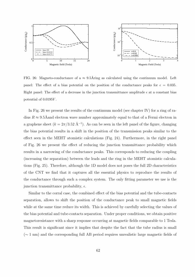
0 5 10 15 20
Magnetic field (Tesla)
0
0.5
1C
ondu
ctan
ce (
g/g 0)
bias=0Vbias=0.015Vbias=0.017V
0 1 2 3 4
Magnetic Field (Tesla)
10-2
10-1
100
Con
duct
ance
(g/
g 0)
ε=0.4ε=0.02ε=0.005
FIG. 26: Magneto-conductance of a ≈ 9.5Aring as calculated using the continuum model. Left
panel: The effect of a bias potential on the position of the conductance peaks for ε = 0.035.
Right panel: The effect of a decrease in the junction transmittance amplitude ε at a constant bias
potential of 0.0195V .
In Fig. 26 we present the results of the continuum model (see chapter IV) for a ring of ra-
dius R ≈ 9.5Aand electron wave number approximately equal to that of a Fermi electron in
a graphene sheet (k = 2π/3.52 A−1). As can be seen in the left panel of the figure, changing
the bias potential results in a shift in the position of the transmission peaks similar to the
effect seen in the MEHT atomistic calculations (Fig. 24). Furthermore, in the right panel
of Fig. 26 we present the effect of reducing the junction transmittance probability which
results in a narrowing of the conductance peaks. This corresponds to reducing the coupling
(increasing the separation) between the leads and the ring in the MEHT atomistic calcula-
tions (Fig. 25). Therefore, although the 1D model does not poses the full 2D characteristics
of the CNT we find that it captures all the essential physics to reproduce the results of
the conductance through such a complex system. The only fitting parameter we use is the
junction transmittance probability, ε.
Similar to the corral case, the combined effect of the bias potential and the tube-contacts
separation, allows to shift the position of the conductance peak to small magnetic fields
while at the same time reduce its width. This is achieved by carefully selecting the values of
the bias potential and tube-contacts separation. Under proper conditions, we obtain positive
magnetoresistance with a sharp response occurring at magnetic fields comparable to 1 Tesla.
This result is significant since it implies that despite the fact that the tube radius is small
(∼ 1 nm) and the corresponding full AB period requires unrealistic large magnetic fields of
62
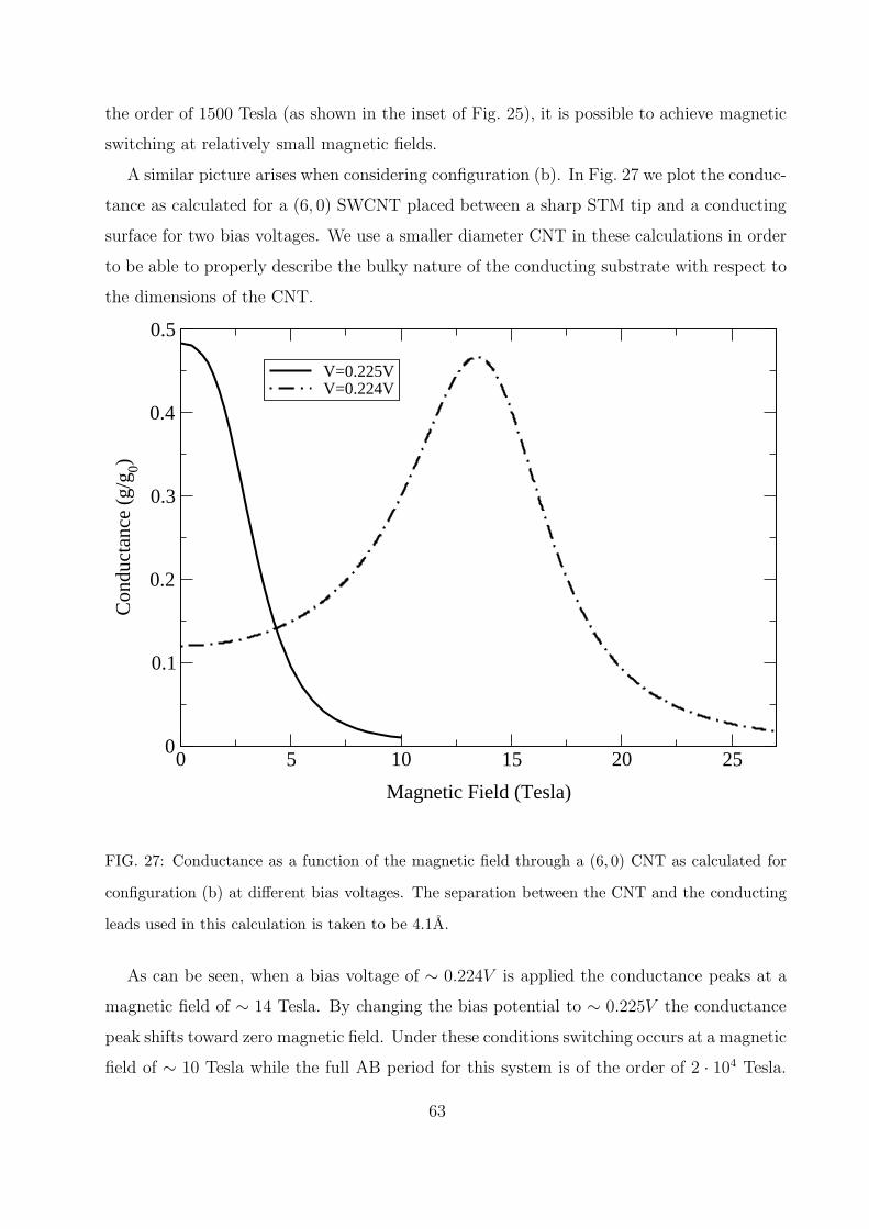
the order of 1500 Tesla (as shown in the inset of Fig. 25), it is possible to achieve magnetic
switching at relatively small magnetic fields.
A similar picture arises when considering configuration (b). In Fig. 27 we plot the conduc-
tance as calculated for a (6, 0) SWCNT placed between a sharp STM tip and a conducting
surface for two bias voltages. We use a smaller diameter CNT in these calculations in order
to be able to properly describe the bulky nature of the conducting substrate with respect to
the dimensions of the CNT.
0 5 10 15 20 25
Magnetic Field (Tesla)
0
0.1
0.2
0.3
0.4
0.5
Con
duct
ance
(g/
g 0)
V=0.225VV=0.224V
FIG. 27: Conductance as a function of the magnetic field through a (6, 0) CNT as calculated for
configuration (b) at different bias voltages. The separation between the CNT and the conducting
leads used in this calculation is taken to be 4.1A.
As can be seen, when a bias voltage of ∼ 0.224V is applied the conductance peaks at a
magnetic field of ∼ 14 Tesla. By changing the bias potential to ∼ 0.225V the conductance
peak shifts toward zero magnetic field. Under these conditions switching occurs at a magnetic
field of ∼ 10 Tesla while the full AB period for this system is of the order of 2 · 104 Tesla.
63

The CNT-leads separation required to achieve high magnetoresistance sensitivity in this
configuration is larger than the one needed for configuration (a). This is due to the difference
in the CNT diameters and the different leads geometries. As the diameter of the tube
becomes smaller, the magnetic field needed to gain a similar AB phase shift grows larger.
Therefore, the conductance peaks become wider so that larger CNT-leads separations are
required in order to narrow their width. Furthermore, as the lead becomes more bulky its
coupling to the CNT needs to be decreased in order to achieve the same magnetoresistance
sensitivity.
To conclude the CNT AB interferometry part, we have demonstrated that SWCNTs can
be used as magnetoresistance switching devices based on the AB effect. As in the corral
setup the essential procedure involves the weak coupling of the SWCNT to the conducting
leads in order to narrow the conducting resonances, while at the same time controlling
the position of the resonances by the application of a bias potential. The control over the
coupling between the SWCNT and the conducting leads in configuration (a) of Fig 23 can
be achieved via a fabrication of a set of leads with proper gaps. In configuration (b) of
the same figure one needs to control the distance between the STM tip and the CNT and
between the substrate and the CNT. The former can be achieved by piezoelectric control
and the latter by covering the surface with monolayer/s of an insulating material.
C. Three terminal devices based on polyaromatic hydrocarbon rings
As discussed in chapter V, an interesting case in which magnetic fields provide unique
control over the conductance is based on the three-terminal setup. Here, we will study the
effects of magnetic field polarity on the selective switching of molecular devices, and show
how such devices can be used for parallel logic operations.62
We consider a polycyclic aromatic hydrocarbon (PAH) hexagonal ring composed of 48
conjugated benzene units with a diameter of ∼ 3nm. Similar PAH molecules have been
synthesized197–199 and studied theoretically,200–203 and the conductance of related organic
molecules attached to gold wires has recently been measured.18 The molecule, is coupled
to three gold atomic wires as shown in Fig. 28, and the geometry of the entire system is
optimized using Fletcher-Reeves/Polak-Ribiere conjugate-gradient algorithm applied to the
MM+ force field on the HyperChem 6.02 software. The transmittance is computed using
64

FIG. 28: A realization of a three terminal molecular AB interferometer based on a polyaromatic
hydrocarbon molecule coupled to three atomic gold wires.
imaginary absorbing potentials as discussed in chapter VIC.
In Fig. 29 we plot the zero bias conductance of the molecular switch as a function of
the magnetic field intensity for both output channels (black and red curves). We focus on
the region of realistic magnetic fields (much smaller than the field required to complete a
full AB period which is ∼ 470 Tesla for a ring with a cross section area of about 8.75nm2).
A relatively large gate voltage, Vg = 1.85V, is needed in order to bring the system into
resonance, and the lead-molecule separation is taken to be ∼ 3A.
For zero magnetic field, both channels are semi-opened and the conductance assumes a
value of 0.4g0 at the selected gate voltage. When a magnetic field of ∼ 2.5 Tesla is applied,
we observe that one output channel fully opens while the other closes shut. As the polarity
of the field changes sign the two output channels interchange their role. Exactly the same
characteristics are captured by the continuum model (e.g. green and blue curves of Fig. 29).
Therefore, it can be seen that the magnetic field polarity serves as a distributor that streams
the electrons to the desired output channel.
Based on this magnetic rectification behavior, it is possible to design a molecular logic
gate which processes two different logic operations simultaneously. This can be achieved by
65

-4 -2 0 2 4
Magnetic Field (Tesla)
0
0.2
0.4
0.6
0.8
1g/
g 0
FIG. 29: Magneto-conductance of the three terminal molecular device shown in Fig. 28. Black and
red curves - conductance of the upper and lower outgoing terminals, respectively, as calculated by
MEHT formalism. Green and blue curves - conductance of the upper and lower outgoing terminals,
respectively, as calculated by the continuum model.
choosing one input signal as the bias voltage (Vb) and the other input signal as the magnetic
field (B). For the bias input signal, Vb, we mark as ′0′ the case where Vb = 0V and as ′1′
the case where a small bias is applied. For the magnetic field input signal we mark as ′0′
the case where B ≈ −3 Tesla and as ′1′ the case where B ≈ 3 Tesla. The output signals are
the currents measured at the two outgoing leads marked as I1 and I2. The following truth
table can be built based on these definitions:
One sees that the output I1 gives the logic operation Vb && B while the output O2
gives the logic operation Vb && B where the over-line stands for NOT. Even though the
conductance peaks are sharp relative to the full AB period, this truth table holds for a wide
range of the threading magnetic field intensity ±(2− 4)Tesla and is thus suitable for robust
66

Vb B I1 I2
0 0 0 0
0 1 0 0
1 0 0 1
1 1 1 0
TABLE I: Truth table for the parallel molecular logic gate.
logic gate operations. Shifting the conductance peaks via the change of the gate potential
will give rise to different logic operations of the same setup.
To summarize the current section, it can be seen that single cyclic molecules are promising
candidates for the fabrication of magnetoresistance parallel switching and gating devices at
feasible magnetic fields. As in the previous discussion, careful fine tuning of experimentally
controllable physical parameters allows the selective switching of a single preselected output
channel. This feature allows the design of a molecular logic gate, processing two logic
operations in parallel.
67
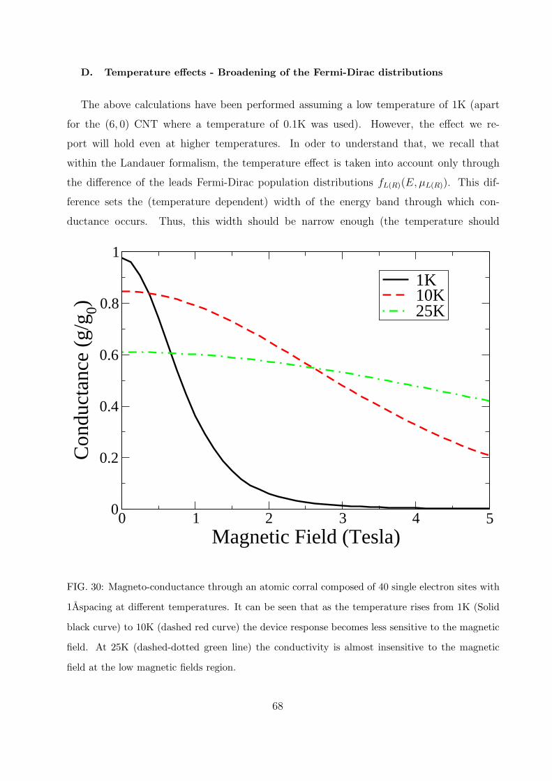
D. Temperature effects - Broadening of the Fermi-Dirac distributions
The above calculations have been performed assuming a low temperature of 1K (apart
for the (6, 0) CNT where a temperature of 0.1K was used). However, the effect we re-
port will hold even at higher temperatures. In oder to understand that, we recall that
within the Landauer formalism, the temperature effect is taken into account only through
the difference of the leads Fermi-Dirac population distributions fL(R)(E, µL(R)). This dif-
ference sets the (temperature dependent) width of the energy band through which con-
ductance occurs. Thus, this width should be narrow enough (the temperature should
0 1 2 3 4 5Magnetic Field (Tesla)
0
0.2
0.4
0.6
0.8
1
Con
duct
ance
(g/
g 0)
1K10K25K
FIG. 30: Magneto-conductance through an atomic corral composed of 40 single electron sites with
1Aspacing at different temperatures. It can be seen that as the temperature rises from 1K (Solid
black curve) to 10K (dashed red curve) the device response becomes less sensitive to the magnetic
field. At 25K (dashed-dotted green line) the conductivity is almost insensitive to the magnetic
field at the low magnetic fields region.
68
be low enough) in order to resolve the magnetic field splitting of the, originally degen-
erate, energy levels of the ring. Using Eq. 11, we find that this splitting is given by
~2
2m?R2
[(−|mF | − φ
φ0
)2
−(|mF | − φ
φ0
)2]
= 2~2mF
m?R2φφ0
= 2~2kF
m?Rφφ0
. Therefore, the temper-
ature should fulfill the following condition in order for AB switching to be observed:
kBT < 2~2kF
m?Rφφ0
.
Considering an atomic corral with a diameter of ∼ 1.3nm and inter-atomic distances
of 1A(40 atomic sites), the normalized magnetic flux at 5 Tesla is, φφ0
≈ 1.5 × 10⁻³, and
the Fermi wavelength is λF ≈ 4A, resulting in a Fermi wave number of kF = 2πλF
≈ π2
A−1. Assuming and effective mass of m? = 1a.u. we get a temperature upper limit of
approximately 7K.
This can be seen in Fig. 30 where the magneto-conductance through such a corral is
calculated using the WBL at different temperatures. The coupling to both leads is taken to
be 0.05eV such that switching occurs at ∼ 5 Tesla. As the temperature rises from 1K (Solid
black curve in the figure) to 10K (dashed red curve in the figure) the device response becomes
less sensitive to the magnetic field even-though an effect is still observable, as predicted. At
a higher temperature of 25K (dashed-dotted green line) the conductivity becomes almost
insensitive to the magnetic field at the magnetic fields region considered.
69

VIII. INELASTIC SCATTERING EFFECTS - MODEL
So far, we have neglected inelastic scattering effects in the treatment of AB interferome-
try in nanometer scale rings. Due to interactions between the conducting electrons and the
vibrational modes of the molecular device (or external phonon modes coupled to the system
for this matter), the phase of the electrons at each pathway on the ring can be randomized
thus reducing coherent interference effects. Therefore, it is important to characterize the rel-
evant physical regime at which inelastic scattering effects are expected to become significant
in molecular based electronic interferometers.
A. Hamiltonian
We consider a tight binding model of an atomic corral based interferometer. As before, we
regard the case of a single valence electron per atomic site. We assume that the interaction
between the electrons and the vibrations occurs on site, namely an electron located at site
i will couple to the local vibration of the ith atom.
The Hamiltonian of the system is given by:
H = Hel + Hvib + Hint, (45)
where Hel is the electronic part of the Hamiltonian, Hvib is the part of the Hamiltonian
describing the vibrational modes of the molecule, and Hint represents the interaction of the
electrons with the vibrations of the molecule.
Before proceeding we shall first give a full description of each of these contributions to
the Hamiltonian.
1. The electronic Hamiltonian
The electronic part of the Hamiltonian may be written as a combination of two terms
Hel = H0el + H int
el where H0el = Hdevice
el + H leadsel , Hdevice
el being the electronic Hamiltonian
of the isolated corral (or any other device), H leadsel the electronic Hamiltonian of the bare
leads, and H intel is the leads-device electronic interaction Hamiltonian. We may write these
terms using second quantization operators. For the non interacting electronic Hamiltonian
70

we have:
H0el =
∑
i,j
ti,jc†icj +
∑
l,m∈L,R
εl,md†ldm, (46)
where c†i , ci, are creation and annihilation operators of an electron on site i on the device,
and d†l and dl are the creation and annihilation operators of an electron on site l on the
relevant lead. ti,j is the hopping integral between site i and site j on the device and εl,m is
the hopping integral between site l and site m on the relevant lead. L and R stand for Left
and right leads.
For the interaction part we have:
H intel =
∑
l,i
Vl,id†l ci +H.c., (47)
where H.c. stands for Hermitian conjugate. The matrix elements of all these terms are
evaluated using the MEHT approach presented in chapter VI.
2. The vibrational Hamiltonian - Normal modes of an atomic chain
When considering the vibrational part of the Hamiltonian, Hvib , we allow the device
atoms to vibrate around their equilibrium position such that we can describe their vibrations
using the harmonic approximation. For the sake of simplicity we also assume that the atoms
are confined to move along the circumference such that we can map the problem onto a one-
dimensional (1D) chain of coupled harmonic oscillators with periodic boundary conditions
as shown in Fig. 31.
FIG. 31: An illustration of a one-dimensional chain of harmonic springs with periodic boundary
conditions. Connecting the rightmost spring with the leftmost mass, is a massless rigid rod of
length N times the equilibrium length of the springs, N being the number of springs.
For the case of a corral composed of identical atoms, the masses, m, and spring constants,
K, in the 1D chain are the same for all sites. Due to the quadratic nature of the harmonic
71

potential it is possible to represent such a 1D chain of identical local springs as a set of
uncoupled non-identical harmonic springs which describe collective motions of the atoms in
the chain. These are usually referred to as the normal vibrational modes of the molecule.
In order to obtain these normal modes we first present the classical vibrational Hamilto-
nian of the system which can be written as follows:
Hvib = Tvib + Vvib =
N−1∑
k=0
P 2k
2m+
1
2K
N−1∑
k=0
(xk+1 − xk)2. (48)
Here, N is the number of atoms and Pk = mxk and xk denote the momentum operator and
the deviation from the equilibrium position of atom k along the chain, respectively. We im-
pose periodic boundary conditions on the system such that xN = x0. For simplicity we define
mass-weight coordinates in the following manner xk ≡ √mxk. Using this transformation
the Hamiltonian can be rewritten in the following form:
Hvib =1
2
N−1∑
k=0
P 2k +
1
2ω2
0
N−1∑
k=0
(xk+1 − xk)2. (49)
Here, Pk = ˙xk and ω0 ≡√
Km
. It is now possible to write the potential energy term appearing
in Eq. 49 using matrix notation:
Vvib =1
2ω2
0
N−1∑
k=0
(xk+1 − xk)2 = ω2
0xT Wx, (50)
where
xT ≡(x0, x1, . . . , xN−1
)(51)
and
W ≡
1 −12
0 0 0 . . . 0 0 0 −12
−12
1 −12
0 0 . . . 0 0 0 0
0 −12
1 −12
0 . . . 0 0 0 0...
......
......
. . ....
......
...
0 0 0 0 0 . . . −12
1 −12
0
0 0 0 0 0 . . . 0 −12
1 −12
−12
0 0 0 0 . . . 0 0 −12
1
. (52)
Let us now denote by U the orthogonal transformation matrix which diagonalizes W such
thatˆW ≡ UW UT is a diagonal matrix, where the diagonal elements are the eigenvalues Ωk
72

(k = 0, . . . , N − 1) of W and UT U = I where I is the unit matrix. We can now write the
potential energy as:
Vvib = ω20x
T UT UW UT Ux = ω20q
T ˆWq = ω2
0
N−1∑
k=0
Ωkq2k ≡
N−1∑
k=0
1
2ω2
kq2k, (53)
where q ≡ Ux and ωk =√
2Ωkω0, and the kinetic energy term as:
Tvib =1
2
N−1∑
k=0
P 2k =
1
2
N−1∑
k=0
PkPk =1
2
N−1∑
k=0
˜xk˜xk =
1
2xT x =
1
2xT UT U x =
1
2qT q. (54)
Finally, the full classical vibrational Hamiltonian is given by:
Hvib = Tvib + Vvib =1
2
N−1∑
k=0
P(q)k
2+
1
2
N−1∑
k=0
ω2kq
2k, (55)
where P(q)k = qk is the canonical momentum conjugated to the coordinates qk. This
Hamiltonian represents a set of N uncoupled harmonic oscillators each with frequency ωk of
the collective normal mode of vibration qk.
Next we consider the quantum mechanical counterpart of the vibrational Hamiltonian
which has exactly the same form as in Eq. 55 except for the canonical momentum which has
the following form: P(q)k = −i~ d
dqk.
It is now possible to define the raising and lowering operators in the following manner:
bk =1√2
[√ωk
~qk + i
1√~ωk
P(q)k
](56)
for the lowering operator, and
b†k =1√2
[√ωk
~qk − i
1√~ωk
P(q)k
](57)
for the razing counterpart. These important operators raise or lower the energy of the
harmonic oscillator by a single quantum. Finally, the vibrational Hamiltonian may be
written in terms of these operators:
Hvib =N−1∑
k=0
~ωk(b†kbk +
1
2). (58)
Therefore, using the transformations described above we have represented a set of local
coupled vibrations using a set of uncoupled normal vibrations. This resembles the trans-
formation from an electronic basis set of localized atomic orbitals to the representation of
orthogonal molecular orbitals.
73

3. The electron-vibrations interaction term
The last term to consider in the full Hamiltonian is the electron-vibration coupling term.
As mentioned, we chose this term to be of the following form:
Hint = MN−1∑
i=0
c†ici(a†i + ai). (59)
Using this form we couple an electron on site i, represented by the number operatorNi ≡ c†ici,
to the local vibration of atom i, represented by a†i + ai. Here a†i and ai are the raising and
lowering operators of the local vibrational modes defined as:ak ≡ 1√
2[√
mω0
~xk + i 1√
m~ω0Pk]
a†k ≡ 1√2[√
mω0
~xk − i 1√
m~ω0Pk],
(60)
such that (a†k + ak) =√
2mω0
~xk =
√2ω0
~
ˆxk. Due to the symmetric nature of the device, we
consider only a single coupling parameter, M , for the coupling between an electron on site
i and the corresponding local vibration. Since we have qi =∑
k Uikxk and UTU = I we can
write xi =∑
k UTikqk =
∑k Ukiqk. Plugging all this into Eq. 59 we have:
Hint = MN−1∑
i=0
c†ici(a†i + ai) = M
N−1∑
i=0
c†ici
√2ω0
~
ˆxi = MN−1∑
i=0
c†ici
√2ω0
~
N−1∑
k=0
Ukiqk
= M
N−1∑
i,k=0
c†ici
√2ω0
~Uki
√~
2ωk(b†k + bk) = M
N−1∑
i,k=0
c†ici
√ω0
ωkUki(b
†k + bk)
=N−1∑
i,k=0
Mki c
†ici(b
†k + bk),
(61)
where we have defined Mki ≡ M
√ω0
ωkUki = M(2Ωk)
− 14Uki.
4. The full Hamiltonian
Collecting all the terms appearing in Eqs. 46, 47, 58, and 61 the full Hamiltonian of the
system is given by the following expression:
H =∑
i,j
ti,jc†icj +
∑
l,m∈L,R
εl,md†ldm + (
∑
l,i
Vl,id†l ci +H.c.)
+
N−1∑
k=0
~ωk(b†kbk +
1
2) +
N−1∑
i,k=0
Mki c
†ici(b
†k + bk).
(62)
74

Hamiltonians similar to the one appearing in Eq. 62 where recently considered in the context
of inelastic electron tunneling spectroscopy150,204–206 and phonon effects in molecular based
transistors207. The only two free parameters in this Hamiltonian are M - the local coupling
strength between an electron on site i and the corresponding local vibration, and ω0 - the
local atomic vibrational frequency. In the next section we use the formalism given in [150] for
the calculation of the conductance through the corral in the presence of electron-vibrations
interactions.
B. conductance
The calculation of the conductance in the presence of the interaction of the conducting
electrons with the vibrational modes of the molecular device is done, as before, within the
framework of NEGF formalism.63,150,208–210 Eq. 17 is still valid for calculating the net current
through the device. Nevertheless, the lesser and greater self energies appearing in Eq. 19
have to be replaced by the following expressions:
Σ< = Σ<L + Σ<
R + Σ<vib
Σ> = Σ>L + Σ>
R + Σ>vib,
(63)
which results in the following current formula:
I = Iel + Iinel. (64)
Here the elastic part is given by a Landuer-like expression:150
Iel =2e
~
∫dE
2πTr Σ<
L (E)Grd(E) [Σ>
L(E) + Σ>R(E)]Ga
d(E) − Σ>L(E)Gr
d(E) [Σ<L (E) + Σ<
R(E)]Gad(E)
=2e
~
∫dE
2π[fL(E, µL) − fR(E, µR)]Tr [ΓL(E)Gr
d(E)ΓR(E)Gad(E)]
(65)
and the inelastic contribution is:150
Iinel =2e
~
∫dE
2πTr [Σ<
L (E)Grd(E)Σ>
vib(E)Gad(E) − Σ>
L(E)Grd(E)Σ<
vib(E)Gad(E)] . (66)
In Eqs. 65 and 66, the retarded GF is modified to include the vibrational coupling in the
following manner:
Grd(ε) =
[(Gr0
d (ε))−1 − Σr
L(ε) − ΣrR(ε) − Σr
vib(ε)]−1
(67)
and, as before, the advanced counter part is the Hermitian conjugate of the retarded GF.
75

C. Self consistent Born approximation
The calculation of the Green’s functions discussed above involves the solution of a many
body problem. A widely used approximation for solving this problem is the self consistent
Born approximation (SCBA).150,152,211 This approximation effectively sums over an infinite
subset of non-crossing diagrams appearing in the pertubative expansion of the GF.
Within the SCBA framework, the vibrational self energy contributions are given as con-
volutions of the vibrational GFs and the electronic GFs. For the retarded self energy we get
(in what follows we use atomic units):
[Σrvib(E)]ij = i
∑
k1,k2
Mk1i Mk2
j
∫[D<
k1k2(ω)Gr
ij(E − ω) +Drk1k2
(ω)G<ij(E − ω)
+Drk1k2
(ω)Grij(E − ω)]
dω
2π+ δij
∑
k1,k2,i′
Mk1i Mk2
i′ neli′D
rk1k2
(ω = 0)
(68)
and for the lesser and greater self energies:
[Σ≷
vib(E)]
ij= i
∑
k1,k2
Mk1i Mk2
j
∫dω
2πD≷
k1,k2(ω)G≷
ij(E − ω). (69)
In these expression:
neli = −i
∫dE
2πG<
ii(E) (70)
and the retarded phonon Green function is given by:
Dr(ω) =[(Dr
0(ω))−1 − Πr(ω)]−1
, (71)
where the unperturbed retarded phonon Greens function is:
[Dr0]k,k′ (ω) = [Da
0 ]?k,k′ (ω) = δk,k′
[1
ω − ωk + iη− 1
ω + ωk + iη
], (72)
η being the vibrational mode energy broadening due to its relaxation to a thermal bath.
This broadening is taken to be constant in the WBL. The retarded phonon SE due to the
interaction with the electrons is given by:
[Πr(ω)]ij = −i∑
i1,i2
M ii1M j
i2
∫dE
2π
[G<
i1,i2(E)Ga
i2,i1(E − ω) +Gr
i1,i2(E)G<
i2,i1(E − ω)
]. (73)
The advanced phonon Green function is the conjugate transpose of the retarded one:
Da(ω) = Dr(ω)†, (74)
76

while lesser (and greater) phonon Green function in Eqs. 68 and 69 is given by:
D≷(ω) = Dr(ω)Π≷(ω)Da(ω). (75)
The lesser and greater phonon SEs are:
[Π≷(ω)
]ij
= −i∑
i1,i2
M ii1M j
i2
∫dE
2πG≷
i1,i2(E)G≶
i2,i1(E − ω). (76)
Since the evaluation of the self energies involves the electronic GFs which themselves
include the self energies, the calculation is done self consistently, using the uncoupled (to
the vibrations) GFs as a starting point, until convergence is reached.
D. First Born approximation
In our calculations we use the first Born approximation, which actually can be viewed as
the first iteration of the SCBA scheme. Within this approximation we replace the electronic
and the vibrational GFs appearing in Eqs. 68 and 69 by their zero order counterparts to
get:
[Σrvib(E)]ij = i
∑
k
Mki M
kj
∫[D<
0 ]k,k (ω) [Gr0]ij (E − ω) + [Dr
0]k,k (ω) [G<0 ]ij (E − ω)
+ [Dr0]k,k (ω) [Gr
0]ij (E − ω)dω2π
+ δij∑
k,i′
Mki M
ki′n
el0,i′ [D
r0]k,k (ω = 0),
(77)
with nel0,i = −i
∫dE2π
[G<0 ]ii (E). And for the lesser and greater self energies:
[Σ≷
vib(E)]
ij= i
∑
k
Mki M
kj
∫dω
2π
[D≷
0
]k,k
(ω)[G≷
0
]ij
(E − ω). (78)
The zero order lesser and greater vibrational GFs are given in terms of the retarded and
advanced zero order vibrational GFs:D<
0 (ω) = F (ω) [Dr0(ω) −Da
0(ω)] sgn(ω)
D>0 (ω) = F (−ω) [Dr
0(ω) −Da0(ω)] sgn(ω),
(79)
where sgn(ω) is the sign of ω and F (ω) is given by:
F (ω) =
N(|ω|) ω > 0
1 +N(|ω|) ω < 0.(80)
77

In the above equations N(ω) = [exp(ω/kBT ) − 1]−1 is the Bose-Einstein distribution func-
tion, and the zero order electronic GFs are the pure electronic terms without the electron-
vibrations interactions as discussed in chapter VI.
The last term in Eq. 77 appears only in finite systems and is referred to as the Hartree
term. In our calculations we neglect this term since it contributes a constant shift to the
energy levels which can be compensated experimentally by the application of a gate potential.
One should keep in mind that the first Born approximation is a truncation of the self-
consistent Born procedure which by itself is an approximation to the solution of the real
many-body problem. Therefore, only the low electron-phonon coupling regime can be con-
sidered within the framework of this model.
E. Numerical considerations
The computational efforts involved in the calculation of the conductance can be consid-
erably reduced if one notices that at low temperature and in the zero bias limit, the only
energy levels contributing to the conductance process are those close to the Fermi energy of
the leads (which is tuned in our calculations to equal the Fermi energy of the device). This
is true if the energy level spacing is much larger then their width and than the difference in
the chemical potentials of the leads. When calculating the conductance through molecular
Aharonov-Bohm interferometers it is also necessary to require that the magnetic fields are
small with respect to the full AB period such that higher or lower levels do not shift into
resonance with the leads in the magnetic field range studied. Fortunately, this is exactly the
case for our calculations. Therefore, it is sufficient to take into consideration only the two
degenerate energy levels which are tuned into resonance at zero magnetic field. For this we
have to transform all our matrices from the atomic basis to the molecular basis and truncate
the molecular basis matrices accordingly.
We denote by V the matrix which diagonalizes the device Hamiltonian and overlap ma-
trices such that Hd = V †HV is a diagonal matrix of the eigenvalues and V †SV = I where
I is the unit matrix.
The transformation of the retarded device GF into the molecular basis set is therefore
78

given by:
Grd =
(ES −H +
1
2iΓL +
1
2iΓR − Σr
vib
)−1
=
[(V †)−1
V †(ES −H +
1
2iΓL +
1
2iΓR − Σr
vib
)V V −1
]−1
=
[(V †)−1
(E − H +
1
2iΓL +
1
2iΓR − Σr
vib
)V −1
]−1
= V
(E − H +
1
2iΓL +
1
2iΓR − Σr
vib
)−1
V †
= V GrdV
†,
(81)
where we have defined, Grd ≡
(E − H + 1
2iΓL + 1
2iΓR − Σr
vib
)−1
, ΓL(R) ≡ V †ΓL(R)V , and
Σrvib ≡ V †Σr
vibV . From Eq. 81 we find that the transformation of the retarded GF to the
molecular basis set is given by Grd = V −1Gr
d
(V †)−1
. In a similar manner it is easy to show
that Gad =
(Gr
d
)†.
The current expressions appearing in Eqs. 65 and 66 can be now written in the molecular
basis. For the elastic part we have:
Iel =2e
~
∫dE
2π[fL(E, µL) − fR(E, µR)]
Tr[(V †)−1V †ΓL(E)V V −1Gr
d(E)(V †)−1V †ΓR(E)V V −1Gad(E)
], (82)
which by performing a cyclic permutation in the trace multiplication and using the trans-
formations defined above becomes:
Iel =2e
~
∫dE
2π[fL(E, µL) − fR(E, µR)]Tr
[ΓL(E)Gr
d(E)ΓR(E)Gad(E)
]. (83)
For the inelastic contribution we can write in a similar manner:
Iinel =2e
~
∫dE
2πTr[Σ<
L(E)Grd(E)Σ>
vib(E)Gad(E) − Σ>
L(E)Grd(E)Σ<
vib(E)Gad(E)], (84)
where the lesser and greater self energies transform to the molecular basis set in the same
manner the retarded and advanced counterparts do: Σ≷L(R) = V †Σ≷
L(R)V and Σ≷vib = V †Σ≷
vibV .
The expressions given in Eqs. 77 and 78 apply only for the case where for each vibrational
mode k, Mk is a diagonal matrix. When transforming to the molecular basis set we have to
rewrite these expressions in a general matrix form:
Σrvib(E) = i
∑
k
∫Mk [D<
0 ]k,k (ω)Gr0(E − ω) + [Dr
0]k,k (ω)G<0 (E − ω)
+ [Dr0]k,k (ω)Gr
0(E − ω)Mk dω
2π,
(85)
79

where we have omitted the Hartree term, and,
Σ≷vib(E) = i
∑
k
∫dω
2πMk
[D≷
0
]k,k
(ω)G≷0 (E − ω)Mk. (86)
The transformed self energies are, therefore, given by:
Σrvib(E) = V †Σr
vib(E)V
= i∑
k
∫Mk[D<
0 ]k,k (ω)Gr0(E − ω) + [Dr
0]k,k (ω)G<0 (E − ω)
+ [Dr0]k,k (ω)Gr
0(E − ω)Mk dω
2π
(87)
and
Σ≷vib(E) = V †Σ≷
vib(E)V = i∑
k
∫dω
2πMk
[D≷
0
]k,k
(ω)G≷0 (E − ω)Mk, (88)
where Mk = V †MkV , and G≷0 transform the same as Gr
0. Eqs. 87 and 88 can now be written
for each matrix element as:
[Σr
vib
]nm
(E) = i∑
k
∑
pq
∫Mk
np[D<0 ]k,k (ω)Gr
0 pq(E − ω) + [Dr0]k,k (ω)G<
0 pq(E − ω)
+ [Dr0]k,k (ω)Gr
0 pq(E − ω)Mkqm
dω
2π
(89)
and [Σ≷
vib
]nm
(E) = i∑
k
∑
pq
∫dω
2πMk
np
[D≷
0
]k,k
(ω)G≷0 pq(E − ω)Mk
qm. (90)
We can now truncate the electronic GFs to include as many energy levels as desired.
If, for example, we would like to include only two levels in our calculation marked as a
and b then the electronic GFs would be truncated as Gpq → Gpq(δpa + δpb)(δqa + δqb) =
Gpq
∑bi=a
∑bj=a δpiδqj . For the more general case we have:
Gpq → Gpq
∑
i∈A
∑
j∈A
δpiδqj, (91)
where A is the sub block of relevant energy levels included in the conductance calculation.
Finally, plugging the truncated version of the GFs given in Eq. 91 in Eqs. 89 and 90,
changing summation indices, and reorganizing the terms, results in the truncated version of
the vibrational self energies calculation: Eqs. 87 and 88 can be now written for each matrix
80

element as:
[Σr
vib
]nm
(E) = i∑
k
∑
pq∈A
MknpM
kqm
∫[D<
0 ]k,k (ω)Gr0 pq(E − ω) + [Dr
0]k,k (ω)G<0 pq(E − ω)
+ [Dr0]k,k (ω)Gr
0 pq(E − ω)dω2π
(92)
and [Σ≷
vib
]nm
(E) = i∑
k
∑
pq∈A
MknpM
kqm
∫dω
2π
[D≷
0
]k,k
(ω)G≷0 pq(E − ω). (93)
As mentioned above, in our case due to the confinement, the ring energy levels spacing
is large. This spacing is much larger than the width of each energy levels since we are
considering low coupling of the device to the leads and of the electrons to the vibrations.
Therefore, at low temperatures and for magnetic fields much smaller than the full AB period,
the zero bias conductance can be calculated using only the two degenerate energy levels
which are in resonance with the leads in the absence of the magnetic field. Thus, using the
truncation methodology presented above, the conductance calculation becomes independent
of the device dimensions. Furthermore, this procedure reduces the computational time and
the required allocated memory, significantly.
81

IX. INELASTIC SCATTERING EFFECTS - RESULTS
In the previous chapter the basic computational tools that allow the investigation of the
conductance through a molecular device in the presence of electron-vibrations interactions
were introduced. In the current chapter we shall present results of numerical calculations
conducted using these tools, for the magneto-conductance of an atomic corral including the
coupling to the vibrations.
We consider a tight binding model of an atomic corral composed of 40 sites. The sites
are identical and monovalent such that each site contributes a single electron. Only two
sites, which are separated by 1800, are coupled to the external electronic reservoirs. These
reservoirs are treated within the wide band limit150 and are represented as constant diagonal
matrices in the atomic basis set. The only non vanishing element in these matrices is
the diagonal element, γL(R), which corresponds to the atomic site coupled to the relevant
reservoir. This element has the dimensions of energy and is identified as the coupling strength
to the relevant lead. After transforming to the molecular basis set we truncate all matrices
to include only two energy levels, as discussed above.
Since the corral is of 4n type, it is expected to conduct in the absence of an external
magnetic field. The coupling to each of the leads is chosen to be γL = γR = 0.05eV such
that the magneto-conductance switching in the absence of electron-vibrations interactions
is obtained at ∼ 5 Tesla.
First we investigate the influence of electron-vibrations coupling on the gate voltage
dependence of the zero-bias, zero-temperature conductance in the absence of a magnetic
field. A similar calculation was recently conducted by Mitra, Aleiner and Millis207 for a
single level coupled to a single vibrational mode. The results obtained in Fig. 11 of reference
[207] are reproduced in Fig. 32. Since our calculation is done via numerical integrations, we
do not work at absolute zero temperature. Nevertheless, we choose the temperature to be
as low as 0.1K such that kBTΓ
≈ 1.7× 10⁻³ << 1. Thus, for any practical consideration this
can be considered as the zero temperature limit. The vibrational frequency, ω0, is taken
to give ~ω0 = 0.01eV, the coupling to the leads is considered to be symmetric such that
ΓL = ΓR = 0.25~ω0 and Γ = ΓL+ΓR = 0.5~ω0, and the width of the vibrational energy levels
due to their relaxation to an external thermal bath is taken as η = 2× 10⁻⁴eV. We plot the
conductance as a function of the gate potential for the case of no vibrational coupling (MΓ
=0)
82

and for the case where the coupling of the electron to the nuclear vibrations of the device
equals the coupling of the device to the leads (MΓ
= 1), where M is the coupling strength to
the vibrational mode. The latter condition defines the upper limit for the relevance of the
pertubative treatment discusses in the last chapter.207
-0.02 -0.01 0 0.01 0.02
Gate Voltage (eV)
0
0.2
0.4
0.6
0.8
1
Con
duct
ance
(g/
g 0)
M/Γ=0M/Γ=1
FIG. 32: Conductance vs. gate voltage for a single energy level coupled to two electronic reservoirs
in the absence (solid black curve) and the presence (dashed red curve) of an interaction with a
single vibrational mode.
As can be seen in Fig. 32 the Lorentzian line-shape of the gate voltage dependent conduc-
tance widens due to the interaction with the vibrational mode. Since at equilibrium the zero
energy imaginary part of the vibrational contribution to the retarded electronic self energy
(Σrvib) vanishes, we find that this broadening results mainly from the real part of Σr
vib.
In Fig. 33 a similar plot is presented for the two degenerate levels of the atomic corral.
Here, the frequency of the local vibrations is taken to be ω0 = 0.0124eV, the vibrational
energy levels broadening is η = 2 × 10⁻⁴eV, the leads coupling parameter is γ = γL + γR =
83

0.1eV and the coupling of the electrons to the local vibrations equals the coupling to the
electronic reservoirs (Mγ
= 1). As can be seen, the picture that arises in the corral case
-0.01 -0.005 0 0.005 0.01
Gate Voltage (eV)
0
0.2
0.4
0.6
0.8
1
Con
duct
ance
(g/
g 0)
M/γ=0M/γ=1
FIG. 33: Conductance vs. gate voltage for a 40 sites atomic corral coupled to two electronic
reservoirs in the absence (solid black curve) and the presence (dashed red curve) of electron-
vibrations interactions.
(Fig. 33) resembles that obtained for a single level (Fig. 32). The difference in the width of
the line-shapes between the two cases results from the fact that the coupling to the electronic
reservoirs is different and that the coupling strength of the molecular levels to the vibrations
in the corral case is not given by M itself but by a set of transformations involving M .
Next we fix the gate voltage to zero, such that at zero magnetic field the corral fully
conducts, and study the magneto-conductance spectrum as a function of the electronic
coupling to the local vibrations, M , and the temperature. In Fig. 34 the zero-bias magneto-
conductance is plotted at a temperature of 1K, and γ = 0.1eV. As can be seen, for extremely
low coupling of M = 0.05γ (dashed red curve in the figure), we see no significant influence
84

0 1 2 3
Magnetic Field (Tesla)
0
0.2
0.4
0.6
0.8
1C
ondu
ctan
ce (
g/g 0)
M/γ=0M/γ=0.05M/γ=0.25M/γ=0.5M/γ=1.0
FIG. 34: Low magnetic field magneto-conductance spectrum of a 40 sites corral at 1K and for
different vibrational coupling strengths. Black curve - no coupling, dashed red curve - Mγ = 0.05,
dashed dotted green curve - Mγ = 0.25, dashed double dotted blue curve - M
γ = 0.5, and double
dashed dotted brown curve - Mγ = 1.0. Here, γ = 0.1eV.
on the magneto-conductance spectrum. However, unlike the case of the gate voltage depen-
dence, as the vibrational coupling is increased the magneto-conductance spectrum lowers
and becomes narrower. When the coupling is set to M = 0.5γ the width of the magneto-
conductance peak is reduced by a factor of two. This behavior can be explained by the fact
that the high transmittance through the corral at zero magnetic field is a result of a delicate
interference condition between the different paths that an electron travels while transvers-
ing the ring. The coupling to the vibrational modes randomizes the phases of these paths
and thus reduces the interference intensity. In the magneto-conductance spectrum this is
translated to a narrowing of the peak.
In Fig. 35 we present the electron’s transmittance probability appearing in the elastic
85

conduction term, which is the dominant contribution to the overall conductance at the zero
bias limit. As can be seen, when no magnetic field is applied (left panel of the figure), the
-0.01 -0.005 0 0.005 0.01
E-Ef (eV)
0
0.2
0.4
0.6
0.8
1
Tra
nsm
ittan
ce P
roba
bilit
y M/γ=0M/γ=0.25
-0.01 -0.005 0 0.005 0.01
E-Ef (eV)
0
0.2
0.4
0.6
0.8
1
Tra
nsm
ittan
ce P
roba
bilit
y M/γ=0M/γ=0.25
FIG. 35: The energy dependence of the transmittance probability through a 40 sites corral as a
function of the coupling to the vibrations at a temperature of 25K (The rest of the parameters are
kept unchanged). Left panel: no magnetic field. Right panel: B = 5 Tesla. Full black curves - no
vibrational coupling, dashed red curves - Mγ = 0.25
conductance peak slightly narrows (red vs. black curve). Upon applying a magnetic field
of 5 Tesla (right panel of Fig. 35), the conductance peak splits into a doublet. Each peak
corresponding to one of the two energy levels which are shifted out of resonance due to the
magnetic field. An important point to notice is that when coupling the electrons to the
vibrations, the separation between the transmittance peak increases at a given magnetic
field (black peaks vs. red peaks in the right panel of Fig. 35) and thus the conductance
decreases. Again, this shift is attributed mainly to the energy dependence of the real part
of Σrvib(E). The slight asymmetry observed between the two conducting peaks at 5 Tesla
with the vibrational coupling is a numerical artifact which does not effect the results.
A similar picture arises when considering the magneto-conductance at a temperature
of 10K (Fig. 36). As discussed in section VIID, the magneto-conductance peaks become
wider at a higher temperature however the overall effect of the coupling to the vibrational
modes remains the same as that presented for the 1K case. It can be clearly seen in Fig. 36
that the conductance reduces even in the absence of the magnetic field. This is a result of
the narrowing of the transmittance probability line shape discussed above (see left panel of
Fig. 35).
86

0 1 2 3 4 5
Magnetic Field (Tesla)
0
0.2
0.4
0.6
0.8C
ondu
ctan
ce (
g/g 0)
M/γ=0M/γ=0.05M/γ=0.25M/γ=0.5M/γ=1.0
FIG. 36: Low magnetic field magneto-conductance spectrum of a 40 sites corral at 10K and for
different vibrational coupling strengths. Black curve - no coupling, dashed red curve - Mγ = 0.05,
dashed dotted green curve - Mγ = 0.25, dashed double dotted blue curve - M
γ = 0.5, and double
dashed dotted brown curve - Mγ = 1.0. Here, γ = 0.1eV.
To summarize, we find, as expected, that the gate voltage dependence of the conductance
broadens upon switching on the electron-vibrations coupling. Nevertheless, the magneto-
conductance peaks reduce both in size and in width when the vibrational coupling is taken
into account. This implies a higher sensitivity of the device to the application of an external
magnetic field, than that predicted for the pure coherent case.
87
X. SUMMARY AND PROSPECTS
Our current understanding of the physics underlying the process of electronic transport
through a single molecule, even though highly addressed during the past few decades, is
still far from complete. The rapid development in molecular junction fabrication in recent
years has opened the way for exciting experimental measurements of conductance through a
single molecule. This has drawn a lot theoretical and technological attention for the possible
utilization of single molecules as miniature electronic components.
External electric fields are often considered when planning a controllable molecular de-
vice. Nevertheless, even though Zeeman splitting and the Kondo effect in single-molecule
devices have been studied, the utilization of magnetic fields in molecular electronics has
been much less explored. Especially, exploiting the Aharonov-Bohm effect in order to con-
trol the conductance through nanometer scale molecular systems was regarded impossible.
This is due to the fact that the nanometric dimensions of cyclic molecular systems should,
in principle, require extremely high magnetic fields to influence the conductance.
In the present study we have outlined a way to circumvent some technological limitations
that where thought to prevent the current application of AB interferometry in nanoscale
devices and presented the physical conditions at which significant magnetoresistance effects
in nanometer scale electronic interferometers are expected to be found.
Using a one-dimensional scattering theory continuum model of an AB interferometer,
which captures the essential physical features of the problem, we have been able to identify
and isolate the important parameters that allow the magnetic control over the conductance
through a nanometer scale ring. We find that in contrast to the constant strive to gain better
coupling between the leads and the molecule within the molecular junction, such magnetic
control in the nanometer scale can be obtained only when this coupling is weak. This results
in a resonant tunneling junction in which the weakly coupled (and thus extremely narrow)
energy levels of the ring allow the transport only at well defined resonance energy values.
By the application of a gate voltage it is possible to tune these resonances such that in the
absence of a magnetic field the device will fully conduct. Turning on a magnetic field will
shift the narrow doubly degenerate energy levels of the ring out of resonance with the leads
and thus will lower the conductance considerably. Therefore, considering the combined effect
of increasing the lifetime of the electron on the ring (through the coupling) and controlling
88

its energy (using a gate voltage), we are able to narrow the magneto-conductance peaks in
the AB spectrum while at the same time shift them toward the low magnetic field regime.
In such a way it should be possible to gain high sensitivity of the conductance through a
nanometer AB ring to a, relatively low ¶¶¶, threading magnetic field. This is despite the
fact that the full AB period involves magnetic fields orders of magnitude higher.
The importance of using magnetic fields rather than electric fields to control the con-
ductance was stressed through the example of a three terminal device. In such a device
the unique symmetry breaking nature of the magnetic vector potential allows the selective
control over the outgoing route of the electron. The magnetic field polarity becomes an
important control parameter which determines through which of the two outgoing leads the
electrons will transverse the ring.
In order to validate the basic principles revealed by the continuum model we have de-
veloped a magnetic extended Huckel theory which allows the atomistic calculation of the
conductance through molecular setups under the influence of an external magnetic field.
Since we are interested in understanding the general physical phenomena, we are less con-
cerned about the fine details of the electronic structure of the system. Therefore, we have
chosen to rely on the extended Huckel Hamiltonian for our basic electronic structure calcula-
tion. To that we added the appropriate magnetic terms which were evaluated analytically in
a gauge invariant Slater type orbitals basis set. We have calculated the transmittance prob-
ability using both the imaginary absorbing potentials method and non-equilibrium Green’s
function techniques. The conductance was then calculated using the Landauer formalism.
Similar to the conclusions drawn by the continuum model, our atomistic calculation re-
sults indicate that nanometer scale circular setups such as an atomic corral or the cross
section of a carbon nanotube can be used for AB interferometry. At a proper combination
of coupling and gate/bias voltage the conductance through the device becomes very sen-
sitive to the magnetic field. Therefore, one can suggest the application of such devices as
electromagnetic switches or as miniature magnetic sensors. Furthermore, when extending
our interest to the three terminal case and applying the same principles discussed above,
we have been able to design a molecular setup that acts as a logic gate that simultaneously
processes two different logic operations. One can only imagine the immense possibilities of
¶¶¶ relative to the full AB period and to the current experimental achievable magnetic fields upper limit.
89
networking such devices.
The important issue of the effect of coupling the electron motion to the nuclear motion
on the coherent nature of the transport through nanometer scale electronic interferometers
was addressed. Since AB magnetoresistance oscillations have been measured, at low tem-
peratures, even at the micrometer scale, it is evident that inelastic scattering events do not
totally wipe out the coherent nature of the transport. The situation is expected to be much
better at the nanometer scale where the frequency of inelastic scattering events is much
lower under similar conditions. A careful planning of the experimental setup, using materi-
als which have long Fermi wavelength and low decoherence length scales should allow for the
measurements of the AB effect even at reasonably high temperatures. Using a tight binding
model of an atomic corral, in which local electron-vibrations coupling is allowed, we study
the magneto conductance dependence on the vibrational coupling. This model was shown
to be equivalent to a problem recently studied, where a set of energy levels was coupled to
a set of vibrational modes. We calculated the conductance using non-equilibrium Green’s
function formalism. The Born approximation was used to solve the many-body problem,
which arises in the calculation of the electron-vibrations coupling effects. We have found
that the gate dependence of the conductance is broadened due to the vibrational coupling.
This result was shown to be expected by considering a reduced model of a single level cou-
pled to a single vibrational mode. Nevertheless, the magneto-conductance trough the device
becomes more sensitive to the application of an external magnetic field. This is explained
by the fact that the coherent nature of the transport is impaired, which results in reduced
interference intensity. We find this effect to sustain even at temperatures as high as 10K for
the case studied. Therefore, even in the presence of vibrational coupling it should, in prin-
ciple, be possible (at least at the low coupling limit studied here) to utilize the nanometer
scale electronic interferometers discussed above in future miniaturized electronic devices.
Many important issues are still to be addressed. One of them involves the investigation
of coherent effects in the presence of electron-vibrations interactions in the high coupling
regime. In this regime it is possible that the coherent nature of the transport would be
destroyed such that no interference effects would be observable at all. Therefore, it is
important to identify the physical conditions at which such effects are expected to be found.
The theoretical investigation of this problem remains a physically interesting issue as well as
a theoretical challenge. Another interesting issue still to be taken into consideration is the
90
effect of the spin of the current carrying particles. Since opposite spins respond differently
when entering a magnetic field region, one would expect that their AB interference patterns
would be different. Using a three terminal setup, it might be possible to design a spin splitter
in which each spin species will transverse the ring through a different outgoing channel. One
other point not yet addressed is the comparison of electron versus hole magneto-conductance.
It is not obvious that the conclusions drawn above for negative charge carrying particles are
valid when considering positive charge conductance. Research in these directions is part of
our present and future plans.
91

APPENDIX A: ANALYTIC EXPRESSIONS FOR THE OVERLAP INTEGRALS
OVER REAL SLATER TYPE ORBITALS
There has been a considerable amount of work dedicated to the development of analytic
expressions for different integrals over the STO basis set. Usually, the main goal is to express
these integrals in terms of the overlap integrals which themselves can be put in simple
analytical forms.169–173,212–223 It is the purpose of the current appendix to give a rigorous
and full description of the analytical treatment of the overlap integrals between each pair
of arbitrary STOs, while correcting a few typing mistakes that have been published in the
literature and may cause some confusion when trying to implement the equations in actual
calculations.
We consider the real STO basis set which consists of a set of atomic orbitals of the
following form165,166:
|n, l,m〉α =(2ζ)n+0.5
√(2n)!
rn−1α e−ζrα ·
(−1)m√
2
(Yl,m(θ, φ) + Y ?
l,m(θ, φ))
m > 0,
Yl,0(θ, φ) m = 0,
(−1)m
i√
2
(Yl,−m(θ, φ) − Y ?
l,−m(θ, φ))
m < 0.
(A1)
Here, (rα, θ, φ) are spherical coordinates centered at the position of atom α, Yl,m(θ, φ) are
the complex spherical harmonics, i =√−1, and ζ = Z−s
n? , Z being the nuclear charge, s - a
screening constant and n? - an effective principal quantum number.
We treat separately three different possibilities of orbital alignments. In section A1 we
consider the overlap of two STOs situated on the same atomic center. Section A2 is devoted
to the overlap expressions between two STOs which are situated upon atomic centers having
a common Z axis. Finally, in section A3, the general overlap integrals are given as a linear
combination of appropriate rotations of the coaxial overlap integrals.
It should be noted that the full details of the mathematical treatment leading to the
following overlap terms are out of the scope of this work. Presented below are only the final
expressions.
1. single center overlap integrals
In the case of the real hydrogen-like orbitals which consist a full orthonormal basis set the
single center overlap integrals are simply given by α〈n2, l2, m2|n1, l1, m1〉α = δn1,n2δl1,l2δm1,m2
92

where δ is the Kronecker delta function. The STOs given in Eq. A1 are a modified version of
the real hydrogen-like orbitals which differ from the original orbitals only in the radial part.
These node-less functions simplify considerably the calculation of most integrals involved in
electronic structure calculations. However, they do not obey the orthonormality condition,
and thus their overlap should be considered explicitly.
Due to the fact that the STOs have the same angular behavior as the hydrogen-like
orbital, their single center orthonormality with respect to the angular quantum numbers is
conserved. Integration with respect to the radial part of the STOs presented in Eq. A1 gives
rise to the following overlap expression:
α〈n2, l2, m2|n1, l1, m1〉α =
(2ζ1
ζ1 + ζ2
)n1+0.5
·(
2ζ2ζ1 + ζ2
)n2+0.5(n1 + n2)!√(2n1)!(2n2)!
δl1,l2δm1,m2 . (A2)
Next we consider the case of the overlap between two coaxially aligned STOs.
2. Two coaxial center overlap integrals
When the two STOs reside on different atomic centers with a coinciding Z axis, the
overlap integral is given by the following expression:169,170
β〈n2, l2, m2|n1, l1, m1〉‖α =δm1,m2(−1)l2−λ
√(2n1)!(2n2)!
ρn1+n2+1(1 + t)n1+12 (1 − t)n2+ 1
2 ·
l1∑
α=−λ
l2∑
β=λ
α+β∑
q=0
gqαβ(l1λ, l2λ)Qq
n1−α,n2−β(ρ, t), (A3)
where ρ = 12R(ζ1 + ζ2) , t = ζ1−ζ2
ζ1+ζ2, λ = |m1|, and R = |R| =
[(x2 − x1)2 + (y2 − y1)
2 + (z2 − z1)2]
12 . The functions gq
αβ(l1λ, l2λ) and Qqn1−α,n2−β(ρ, t) are
of the following form:
gqαβ(l1λ, l2λ) = g0
αβ(l1λ, l2λ)Fq(α + λ, β − λ) (A4)
and
QqN1,N2
(ρ, t) =
N1+N2∑
m=0
Fm(N1, N2)AN1+N2+q−m(ρ)Bq+m(ρt). (A5)
Here Fm(N1, N2) is given by (0 ≤ m ≤ N1 +N2):
Fm(N1, N2) = N1!N2!
N2∑
k=0
(−1)k
k!(m− k)!(N2 − k)!(N1 −m+ k)!(A6)
93

and An(ρ) and Bn(ρt) are the auxiliary functions defined by:
Ak(ρ) ≡∫ ∞
1
µke−ρµdµ (A7)
Bk(ρt) ≡∫ 1
−1
νke−ρtνdν (A8)
and determined from the following recursion relations:171,173
Ak(ρ) =
e−r
ρk = 0,
1ρ[kAk−1(ρ) + e−ρ] k > 0.
(A9)
Due to numerical stability issues the recursion relation of Bk(ρt) in the case where t 6= 0
is calculated separately for two regions. When kρt< 1 the recursion is done upwards in the
following manner:
Bk(ρt) =
2ρt
sinh(ρt) k = 0,
1ρt
[kBk−1(ρt) + (−1)keρt − e−ρt
]k > 0.
(A10)
When kρt
≥ 1 the recursion is done downwards:
Bk(ρt) =
2ρt
sinh(ρt) ktop,
1k+1
[(ρt)Bk+1 + (−1)keρt + e−ρt)
]k < ktop.
(A11)
and the value of ktop is determined from the number of significant digits d needed in the
calculation of Bk≤kmax(ρt) in the following form:
ktop ≥
d
|log(kmaxρt )|
+ kmax kmax 6= ρt,
k2max kmax = ρt.
(A12)
When t = 0 the expression reduces to:
Bk(0) =1 + (−1)k
k + 1. (A13)
Finally, the function g0αβ(l1λ, l2λ) in Eq. A4 is given by the following expression:
g0αβ(l1λ, l2λ) =
1
2l1+l2+1
[(2l1 + 1)(l1 − λ)!(2l2 + 1)(l2 − λ)!
(l1 + λ)!(l2 + λ)!
] 12
·
(l1 + β)!(−1)12(l1−α)+ 1
2(l2−β)−λ
[12(l2 − β)]![1
2(l2 + β)]!(β − λ)!
·2λ∑′
i=0
(−1)i2 (l1 + α + 2λ− i)!Fi(λ, λ)[
12(l1 − α) − λ+ i
2
]![
12(l1 + α) + λ− i
2
]!(α+ λ− i)!
.
(A14)
94

The sign∑′
i= 0 designates that the summation is taken only over the even values of i.
g0αβ(l1λ, l2λ) is assigned the value of zero if at least one of the numbers l1±α or l2±β is odd.
It should be noted that in equations A6 and A14 terms with factorials of negative numbers
do not contribute to the summation.
3. General overlap integrals
The full expression for the overlap integral in the general case where the atomic centers
do not necessarily reside on coaxially aligned frames is given in terms of the aligned integrals
using appropriate rotation relations as follows:170,172
β〈n2, l2, m2|n1, l1, m1〉α =
min(l1,l2)∑
λ=0
T ∗λl1m1,l2m2
(Θ,Φ)β〈n2, l2, λ|n1, l1, λ〉‖α. (A15)
The rotation coefficients T ∗λl1m1,l2m2
(Θ,Φ) are given by the following formula (for real STOs):
T λl1m1,l2m2
(Θ,Φ) =2
(1 + δλ0)[(1 + δm10)(1 + δm20)]12
1∑′
i=−1
l1+l2∑′
L=|l1−l2|(εm1,0)
δi,εm1,m2C l1l2Liγ1,γ2,iγ1+γ2
C l1l2Lλ,−λ,0
[2π(1 + δMi0)
2L+ 1
] 12
SLMi(Θ,Φ). (A16)
Here, γi = |mi|, Mi = εm1,m2 |iγ1 + γ2|, and
εm1,m2 =
1 (m1 ≥ 0 and m2 ≥ 0) or (m1 < 0 and m2 < 0),
−1 else.(A17)
The coefficients Cj1j2Jm1,m2,M appearing in Eq. A16 are related to the well known Clebsch-Gordan
coefficients (j1j2m1m2|j1j2JM) by the following relation:
Cj1j2Jm1,m2,M = (−1)
12(|m1|+m1+|m2|+m2+|M |+M)(j1j2m1m2|j1j2JM) (A18)
and SLMi(Θ,Φ) are the real spherical harmonics related to the imaginary counterparts
(YLMi(Θ,Φ)) by:
Slm(Θ,Φ) =(−i)δm,−|m|
√2(1 + δm0)
(Yl|m|(Θ,Φ) + εm,0Yl,−|m|(Θ,Φ)). (A19)
This concludes the full description of the expressions involved in the analytic evaluation
of the overlap integrals over the real STO basis set.
95

APPENDIX B: MAGNETIC TERMS INTEGRALS OVER REAL STOS AS LIN-
EAR COMBINATIONS OF OVERLAP INTEGRALS
Extensive work on the analytical evaluation of magnetic multipole moment integrals over
Slater type orbitals has been done in the context of the calculation of magnetic properties of
molecules224–229. Although general, most of the expressions obtained are usually very com-
plex and hard to implement. In the present work, however, only the lowest order moments
integrals are necessary to be evaluated. Thus, it is useful to develop simple expressions that
will be straightforward to implement in numerical calculations. This appendix is devoted to
the development of such expressions. After somewhat tedious mathematical manipulations
we find expressions for the magnetic terms integrals as simple linear combinations of the
overlap integrals treated in appendix A. A reader interested only in the final expressions is
urged to skip the detailed development presented below and use Eqs. B19, B31, and B39.
As noted before, we choose to apply the external magnetic field parallel to the X axis.
The resulting magnetic linear and quadratic terms in the Hamiltonian (see Eqs. 40 and 41)
are then given by:
Hmaglin = −µB
~LxBx (B1)
and
Hmagquad =
q2B2x
8me
(y2 + z2
). (B2)
Considering the London approximation presented in Eq. 44 we need to evaluate integrals
of the following form: α
⟨n1, l1, m1|Lx|n2, l2, m2
⟩β
and α 〈n1, l1, m1|y2 + z2|n2, l2, m2〉β where
the integration is taken over the regular STOs rather than the gauge invariant STOs. Each
of the magnetic terms will be treated separately in the following sections.
For the following calculations it shall be useful to rewrite the mathematical expression of
the real STOs presented in Eq. A1 in the following form:
|n, l,m〉 = Rn(r)Sl,m(θ, φ), (B3)
where
Rn(r) =(2ζ)n+0.5
√(2n)!
rn−1e−ζr (B4)
96

and
Sl,m(θ, φ) =
(−1)m√
2
(Yl,m(θ, φ) + Y ?
l,m(θ, φ))
m > 0,
Yl,0(θ, φ) m = 0,
(−1)m
i√
2
(Yl,−m(θ, φ) − Y ?
l,−m(θ, φ))
m < 0.
(B5)
Using the following definition of the spherical harmonics:
Yl,m (θ, φ) = (−1)mNl,mPml [cos(θ)]eimφ, (B6)
with
Nl,m ≡[2l + 1
4π
(l −m)!
(l +m)!
] 12
, (B7)
Sl,m(θ, φ) may alternatively be written as:
Sl,m(θ, φ) = 20.5(1−δ|m|,0)Nl,|m|P|m|l [cos(θ)] Φm(φ). (B8)
Here, the longitudinal angular dependence is given by the well known associated Legendre
polynomials P|m|l [cos(θ)] which can be defined using the following generating equation:
Pml (x) =
1
2ll!(1 − x2)
m2dl+m
dxl+m(x2 − 1)l (B9)
and the azimuthal angular dependence is given by:
Φm(φ) =
cos(mφ) m ≥ 0,
sin(|m|φ) m < 0.(B10)
1. Linear magnetic term integrals
For the evaluation of the linear magnetic term integrals α
⟨n1, l1, m1|Lx|n2, l2, m2
⟩β
we
shall use the angular momentum creation and annihilation operators which relate to the
the angular momentum component along the X axis by Lx = 12
(L+ + L−
). Since the
angular momentum operator operates only on the angular coordinates of the STO orbital it
is sufficient to consider its operation on Slm(θ, φ) alone. We use the following equations for
the operation of the creation and annihilation angular momentum operators on the spherical
harmonics:
L+Yl,m = [l(l + 1) −m(m+ 1)]12 ~Yl,m+1 (B11)
L−Yl,m = [l(l + 1) −m(m− 1)]12 ~Yl,m−1. (B12)
97

and the relation between the spherical harmonic function and its complex conjugate Y ?l,m = (−1)mYl,−m, in order to write down
their operation on Sl,m(θ, φ):
L+Sl,m(θ, φ) = ~
(−1)m√
2
[l(l + 1) −m(m+ 1)]
12 Yl,m+1(θ, φ) + (−1)m [l(l + 1) +m(1 −m)]
12 Yl,1−m(θ, φ)
m > 0,
√l(l + 1)Yl,1(θ, φ) m = 0,
(−1)m
i√
2
[l(l + 1) +m(1 −m)]
12 Yl,1−m(θ, φ) − (−1)m [l(l + 1) −m(m+ 1)]
12 Yl,m+1(θ, φ)
m < 0.
(B13)
L−Sl,m(θ, φ) = ~
(−1)m√
2
[l(l + 1) −m(m− 1)]
12 Yl,m−1(θ, φ) + (−1)m [l(l + 1) −m(m+ 1)]
12 Yl,−m−1(θ, φ)
m > 0,
√l(l + 1)Yl,−1(θ, φ) m = 0,
(−1)m
i√
2
[l(l + 1) −m(m+ 1)]
12 Yl,−m−1(θ, φ) − (−1)m [l(l + 1) −m(m− 1)]
12 Yl,m−1(θ, φ)
m < 0.
(B14)
Thus, the operation of Lx on Sl,m is given by:
LxSl,m(θ, φ) =~
2
(−1)m√
2[l(l + 1) −m(m− 1)]
12(Yl,m−1 − Y ?
l,m−1
)+ [l(l + 1) −m(m+ 1)]
12(Yl,m+1 − Y ?
l,m+1
) m > 0,
√l(l + 1)
(Yl,1 − Y ?
l,1
)m = 0,
(−1)m
i√
2
[l(l + 1) −m(m− 1)]
12
(Yl,−(m−1) + Y ?
l,−(m−1)
)+ [l(l + 1) −m(m+ 1)]
12
(Yl,−(m+1) + Y ?
l,−(m+1)
)m < 0,
(B15)

where we have denoted Yl,m(θ, φ) ≡ Yl,m. Using Eq. B5 we can now write this back in terms of the real spherical harmonics:
LxSl,m(θ, φ) =−i~2
[l(l + 1) −m(m− 1)]12 Sl,−(m−1)(θ, φ) + [l(l + 1) −m(m+ 1)]
12 Sl,−(m+1)(θ, φ) m > 1,
[l(l + 1) − 2]12 Sl,−2(θ, φ) m = 1,
√2l(l + 1)Sl,−1(θ, φ) m = 0,
−
[l(l + 1) − 2]12 Sl,2(θ, φ) +
√2l(l + 1)Sl,0(θ, φ)
m = −1,
−
[l(l + 1) −m(m− 1)]12 Sl,−(m−1)(θ, φ) + [l(l + 1) −m(m+ 1)]
12 Sl,−(m+1)(θ, φ)
m < −1.
(B16)
In order to get the operation Lx|n, l,m > it is necessary to multiply the expression obtained in Eq. B16 by Rn(r) to get:
Lx|n, l,m >=−i~2
−
[l(l + 1) − 2]12 |n, l, 2 > +
√2l(l + 1)|n, l, 0 >
m = −1,
√2l(l + 1)|n, l,−1 > m = 0,
[l(l + 1) − 2]12 |n, l,−2 > m = 1,
(−1)δm,|−m|
[l(l + 1) −m(m− 1)]
12 |n, l,−(m− 1) > + [l(l + 1) −m(m+ 1)]
12 |n, l,−(m+ 1) >
else,
(B17)
where we have combined the cases of m > 1 and m < −1. By the further usage of Kronecker δ-functions this expression reduces
to:
Lx|n, l,m > = (−i~)(−1)δm,|−m|
2(1 − δm,0 − δm,1) [l(l + 1) −m(m− 1)]
12 |n, l,−(m− 1) > +
(−√
2)δm,0(√
2)δm,−1 [l(l + 1) −m(m+ 1)]12 |n, l,−(m+ 1) >.
(B18)

Finally, the full linear magnetic term integral can be written as a sum of two overlap integrals as follows:
β
⟨n2, l2, m2|Lx|n1, l1, m1
⟩α
= (−i~)(−1)δm1,|−m1|
2
(1 − δm1,0 − δm1,1) [l1(l1 + 1) −m1(m1 − 1)]12
β 〈n2, l2, m2|n1, l1,−(m1 − 1)〉α +
(−√
2)δm1,0(√
2)δm1,−1 [l1(l1 + 1) −m1(m1 + 1)]12
β 〈n2, l2, m2|n1, l1,−(m1 + 1)〉α.
(B19)

2. Quadratic magnetic term integrals
Evaluating the quadratic magnetic term integrals involves the calculation of expressions
of the form:
α
⟨n1, l1, m1|y2 + z2|n2, l2, m2
⟩β
=
(α〈n1, l1, m1|y)(y|n2, l2, m2〉β) + (α〈n1, l1, m1|z)(z|n2, l2, m2〉β), (B20)
where we have used the fact that the position operators can be operated both on the ket
and on the bra of the integral. Thus it is sufficient to calculate expressions of the form
y|n, l,m > and z|n, l,m >.
For the calculation we shall use the spherical representation of the Cartesian components:
x = r sin(θ) cos(φ)
y = r sin(θ) sin(φ)
z = r cos(θ)
(B21)
and operate them on the real STOs using Eq. B3:
x|n, l,m >= rRn(r) sin(θ) cos(φ)Sl,m(θ, φ)
y|n, l,m >= rRn(r) sin(θ) sin(φ)Sl,m(θ, φ)
z|n, l,m >= rRn(r) cos(θ)Sl,m(θ, φ).
(B22)
The operation of r on the radial part of the STOs in Eq. B22 can be easily written as
the radial part of a STO with a shifted principal quantum number:
rRn(r) =(2ζ)n+0.5
√(2n)!
r(n+1)−1e−ζr =
√(2n+ 1)(2n+ 2)
2ζ
(2ζ)(n+1)+0.5
√[2(n+ 1)]!
r(n+1)−1e−ζr
=
√(2n+ 1)(2n+ 2)
2ζRn+1(r),
(B23)
where we have used the definition given in Eq. B4
To find the operation of the angular operators on the STOs we use the definition of
Sl,m(θ, φ) given in Eq. B8, the following relations for the associated Legendre polynomials:
cos(θ)Pml [cos(θ)] =
(l+m2l+1
)Pm
l−1[cos(θ)] +(
l−m+12l+1
)Pm
l+1[cos(θ)]
sin(θ)Pml [cos(θ)] =
(1
2l + 1
)Pm+1
l+1 [cos(θ)] −(
1
2l + 1
)Pm+1
l−1 [cos(θ)]
=
[(l +m)(l +m− 1)
2l + 1
]Pm−1
l−1 [cos(θ)] −[(l −m+ 1)(l −m+ 2)
2l + 1
]Pm−1
l+1 [cos(θ)]
(B24)
101
and the following trigonometric relations:
sin(φ) sin(|m|φ) = 12cos[(|m| − 1)φ] − cos[(|m| + 1)φ]
cos(φ) sin(|m|φ) = 12sin[(|m| − 1)φ] + sin[(|m| + 1)φ]
sin(φ) cos(|m|φ) = 12sin[−(|m| − 1)φ] + sin[(|m| + 1)φ]
cos(φ) cos(|m|φ) = 12cos[(|m| − 1)φ] + cos[(|m| + 1)φ].
(B25)
First we shall consider the angular part of the operation of z on an STO, z|n, l,m >. From
Eqs. B22 and B8 it is clear that we have to evaluate the following expression:
cos(θ)Sl,m(θ, φ) = 20.5(1−δ|m|,0)Nl,|m| cos(θ)P|m|l [cos(θ)]
cos(mφ) m ≥ 0,
sin(|m|φ) m < 0.(B26)
Using the relation given in Eq. B24 this can be written as:
cos(θ)Sl,m(θ, φ) = 20.5(1−δ|m|,0)Nl,|m|
[(l + |m|2l + 1
)P
|m|l−1 +
(l − |m| + 1
2l + 1
)P
|m|l+1
]
cos(mφ) m ≥ 0,
sin(|m|φ) m < 0,
(B27)
where we have denoted Pml ≡ Pm
l [cos(θ)]. When multiplying and dividing P|m|l−1 by Nl−1,|m|
and P|m|l+1 by Nl+1,|m| this can be rewritten as:
cos(θ)Sl,m(θ, φ) =Nl,|m|Nl−1,|m|
(l + |m|2l + 1
)Sl−1,m(θ, φ) +
Nl,|m|Nl+1,|m|
(l − |m| + 1
2l + 1
)Sl+1,m(θ, φ),
(B28)
which in turn reduces to:
cos(θ)Sl,m(θ, φ) = n1l,mSl−1,m(θ, φ) + n1
l+1,mSl+1,m(θ, φ). (B29)
Defining n1l,m ≡
√(l−m)(l+m)(2l−1)(2l+1)
. Therefore, the full operation of z on a STO is given by a
combination of Eqs. B3, B23 and B29 which yields:
z|n, l,m >=
√(2n+ 1)(2n+ 2)
2ζ
[n1
l,m|n+ 1, l − 1, m > +n1l+1,m|n+ 1, l + 1, m >
]. (B30)
102

The resulting integral can be written as a linear combination of four overlap integrals:
β
⟨n2, l2, m2|z2|n1, l1, m1
⟩α
=
√(2n1 + 1)(2n1 + 2)(2n2 + 1)(2n2 + 2)
4ζ1ζ2
[n1l1,m1
n1l2,m2 β 〈n2 + 1, l2 − 1, m2|n1 + 1, l1 − 1, m1〉α + n1
l1+1,m1n1
l2,m2 β 〈n2 + 1, l2 − 1, m2|n1 + 1, l1 + 1, m1〉α +
n1l1,m1
n1l2+1,m2 β 〈n2 + 1, l2 + 1, m2|n1 + 1, l1 − 1, m1〉α + n1
l1+1,m1n1
l2+1,m2 β 〈n2 + 1, l2 + 1, m2|n1 + 1, l1 + 1, m1〉α]. (B31)
We now turn to calculate the operation y|n, l,m >. Similar to what presented above, the angular operation is given by:
sin(θ) sin(φ)Sl,m(θ, φ) = 20.5(1−δ|m|,0)Nl,|m| sin(θ)P|m|l [cos(θ)] sin(φ)Φm(φ). (B32)
As before, by using Eq. B24 the longitudinal part can be written as:
Nl,|m| sin(θ)P|m|l [cos(θ)] =
±[(l ± |m| + 1)(l ± |m| + 2)
(2l + 1)(2l + 3)
] 12
Nl+1,|m|±1P|m|±1l+1 [cos(θ)] ∓
[(l ∓ |m|)(l ∓ |m| − 1)
(2l − 1)(2l + 1)
] 12
Nl−1,|m|±1P|m|±1l−1 [cos(θ)]. (B33)
The trigonometric relations presented in Eq. B25 give the following result for the azimuthal part:
sin(φ)Φm(φ) =
sin(φ) cos(mφ) m ≥ 0,
sin(φ) sin(|m|φ) m < 0.=
1
2
sin[−(|m| − 1)φ] + sin[(|m| + 1)φ] m ≥ 0,
cos[(|m| − 1)φ] − cos[(|m| + 1)φ] m < 0.
=1
2
sin[(m+ 1)φ] − sin[(m− 1)φ] m > 1,
sin[2φ] m = 1,
2 sin(φ) m = 0,
1 − cos[2φ] m = −1,
cos[(m+ 1)φ] − cos[(m− 1)φ] m < −1.
=1
2
2Φ−1(φ) m = 0,
Φ−2(φ) m = 1,
Φ−(m+1)(φ) − Φ−(m−1)(φ) else.
(B34)

Merging Eqs. B33 and B34 results in the following expressions:
Nl,|m| sin(θ)P|m|l [cos(θ)] sin(φ)Φm(φ) =
1
2
−[
(l−|m|+1)(l−|m|+2)(2l+1)(2l+3)
] 12
Nl+1,|m|−1P|m|−1l+1 [cos(θ)]Φ−(m+1)(φ) +
[(l+|m|)(l+|m|−1)
(2l−1)(2l+1)
] 12
Nl−1,|m|−1P|m|−1l−1 [cos(θ)]Φ−(m+1)(φ)
−[
(l+|m|+1)(l+|m|+2)(2l+1)(2l+3)
] 12Nl+1,|m|+1P
|m|+1l+1 [cos(θ)]Φ−(m−1)(φ) +
[(l−|m|)(l−|m|−1)
(2l−1)(2l+1)
] 12Nl−1,|m|+1P
|m|+1l−1 [cos(θ)]Φ−(m−1)(φ) m < −1
−[
l(l+1)(2l+1)(2l+3)
] 12Nl+1,0P
0l+1[cos(θ)]Φ0(φ) +
[(l+1)l
(2l−1)(2l+1)
] 12Nl−1,0P
0l−1[cos(θ)]Φ0(φ)
−[
(l+2)(l+3)(2l+1)(2l+3)
] 12Nl+1,2P
2l+1[cos(θ)]Φ2(φ) +
[(l−1)(l−2)
(2l−1)(2l+1)
] 12Nl−1,2P
2l−1[cos(θ)]Φ2(φ) m = −1,
2[
(l+1)(l+2)(2l+1)(2l+3)
] 12Nl+1,1P
1l+1[cos(θ)]Φ−1(φ) − 2
[l(l−1)
(2l−1)(2l+1)
] 12Nl−1,1P
1l−1[cos(θ)]Φ−1(φ) m = 0,
[(l+2)(l+3)
(2l+1)(2l+3)
] 12Nl+1,2P
2l+1[cos(θ)]Φ−2(φ) −
[(l−1)(l−2)
(2l−1)(2l+1)
] 12Nl−1,2P
2l−1[cos(θ)]Φ−2(φ) m = 1,
[(l+|m|+1)(l+|m|+2)
(2l+1)(2l+3)
] 12Nl+1,|m|+1P
|m|+1l+1 [cos(θ)]Φ−(m+1)(φ) −
[(l−|m|)(l−|m|−1)
(2l−1)(2l+1)
] 12Nl−1,|m|+1P
|m|+1l−1 [cos(θ)]Φ−(m+1)(φ)
+[
(l−|m|+1)(l−|m|+2)(2l+1)(2l+3)
] 12
Nl+1,|m|−1P|m|−1l+1 [cos(θ)]Φ−(m−1)(φ) −
[(l+|m|)(l+|m|−1)
(2l−1)(2l+1)
] 12
Nl−1,|m|−1P|m|−1l−1 [cos(θ)]Φ−(m−1)(φ) m > 1.
(B35)

Therefore,
sin(θ) sin(φ)Sl,m(θ, φ) =1
2
−[
(l−|m|+1)(l−|m|+2)(2l+1)(2l+3)
] 12
Sl+1,−(m+1)(θ, φ) +[
(l+|m|)(l+|m|−1)(2l−1)(2l+1)
] 12
Sl−1,−(m+1)(θ, φ)
−[
(l+|m|+1)(l+|m|+2)(2l+1)(2l+3)
] 12Sl+1,−(m−1)(θ, φ) +
[(l−|m|)(l−|m|−1)
(2l−1)(2l+1)
] 12Sl−1,−(m−1)(θ, φ) m < −1
−√
2[
l(l+1)(2l+1)(2l+3)
] 12Sl+1,0(θ, φ) +
√2[
(l+1)l(2l−1)(2l+1)
] 12Sl−1,0(θ, φ)
−[
(l+2)(l+3)(2l+1)(2l+3)
] 12
Sl+1,2(θ, φ) +[
(l−1)(l−2)(2l−1)(2l+1)
] 12
Sl−1,2(θ, φ) m = −1,
√2[
(l+1)(l+2)(2l+1)(2l+3)
] 12Sl+1,−1(θ, φ) −
√2[
l(l−1)(2l−1)(2l+1)
] 12Sl−1,−1(θ, φ) m = 0,
[(l+2)(l+3)
(2l+1)(2l+3)
] 12
Sl+1,−2(θ, φ) −[
(l−1)(l−2)(2l−1)(2l+1)
] 12
Sl−1,−2(θ, φ) m = 1,
[(l+|m|+1)(l+|m|+2)
(2l+1)(2l+3)
] 12Sl+1,−(m+1)(θ, φ) −
[(l−|m|)(l−|m|−1)
(2l−1)(2l+1)
] 12Sl−1,−(m+1)(θ, φ)
+[
(l−|m|+1)(l−|m|+2)(2l+1)(2l+3)
] 12Sl+1,−(m−1)(θ, φ) −
[(l+|m|)(l+|m|−1)
(2l−1)(2l+1)
] 12Sl−1,−(m−1)(θ, φ) m > 1.
(B36)
Equation B36 can be further reduced by the application of several Kronecker δ functions to give the following unified expression:
sin(θ) sin(φ)Sl,m(θ, φ) =(−1)δm,−|m|
2(−
√2)δm,0(
√2)δm,−1
[n2
l+1,m+1Sl+1,−(m+1)(θ, φ) − n2l,−mSl−1,−(m+1)(θ, φ)
]
+ (1 − δm,0 − δm,1)[n2
l+1,−(m−1)Sl+1,−(m−1)(θ, φ) − n2l,mSl−1,−(m−1)(θ, φ)
],
(B37)
where we have defined n2l,m ≡
[(l+m−1)(l+m)(2l−1)(2l+1)
] 12.

Finally, adding the radial part one finds that:
y|n, l,m >=(−1)δm,−|m|
√(2n+ 1)(2n+ 2)
4ζ
(−√
2)δm,0(√
2)δm,−1[n2
l+1,m+1|n+ 1, l + 1,−(m+ 1) > −n2l,−m|n+ 1, l− 1,−(m+ 1) >
]+
(1 − δm,0 − δm,1)[n2
l+1,−(m−1)|n+ 1, l + 1,−(m− 1) > −n2l,m|n+ 1, l − 1,−(m− 1) >
].
(B38)

The resulting integral is a linear combination of 16 overlap terms:
β
⟨n2, l2, m2|y2|n1, l1, m1
⟩α
=(−1)δm1,−|m1|
+δm2,−|m2|√
(2n1 + 1)(2n1 + 2)(2n2 + 1)(2n2 + 2)
16ζ1ζ2
(−√
2)δm1,0(√
2)δm1,−1(−√
2)δm2,0(√
2)δm2,−1n2l1+1,m1+1n
2l2+1,m2+1 β 〈n2 + 1, l2 + 1,−(m2 + 1)|n1 + 1, l1 + 1,−(m1 + 1)〉α
− (−√
2)δm1,0(√
2)δm1,−1(−√
2)δm2,0(√
2)δm2,−1n2l1+1,m1+1n
2l2,−m2 β 〈n2 + 1, l2 − 1,−(m2 + 1)|n1 + 1, l1 + 1,−(m1 + 1)〉α
+ (−√
2)δm1,0(√
2)δm1,−1(1 − δm2,0 − δm2,1)n2l1+1,m1+1n
2l2+1,−(m2−1) β 〈n2 + 1, l2 + 1,−(m2 − 1)|n1 + 1, l1 + 1,−(m1 + 1)〉α
− (−√
2)δm1,0(√
2)δm1,−1(1 − δm2,0 − δm2,1)n2l1+1,m1+1n
2l2,m2 β 〈n2 + 1, l2 − 1,−(m2 − 1)|n1 + 1, l1 + 1,−(m1 + 1)〉α
− (−√
2)δm1,0(√
2)δm1,−1(−√
2)δm2,0(√
2)δm2,−1n2l1,−m1
n2l2+1,m2+1 β 〈n2 + 1, l2 + 1,−(m2 + 1)|n1 + 1, l1 − 1,−(m1 + 1)〉α
+ (−√
2)δm1,0(√
2)δm1,−1(−√
2)δm2,0(√
2)δm2,−1n2l1,−m1
n2l2,−m2 β 〈n2 + 1, l2 − 1,−(m2 + 1)|n1 + 1, l1 − 1,−(m1 + 1)〉α
− (−√
2)δm1,0(√
2)δm1,−1(1 − δm2,0 − δm2,1)n2l1,−m1
n2l2+1,−(m2−1) β 〈n2 + 1, l2 + 1,−(m2 − 1)|n1 + 1, l1 − 1,−(m1 + 1)〉α
+ (−√
2)δm1,0(√
2)δm1,−1(1 − δm2,0 − δm2,1)n2l1,−m1
n2l2,m2 β 〈n2 + 1, l2 − 1,−(m2 − 1)|n1 + 1, l1 − 1,−(m1 + 1)〉α
+ (1 − δm1,0 − δm1,1)(−√
2)δm2,0(√
2)δm2,−1n2l1+1,−(m1−1)n
2l2+1,m2+1 β 〈n2 + 1, l2 + 1,−(m2 + 1)|n1 + 1, l1 + 1,−(m1 − 1)〉α
− (1 − δm1,0 − δm1,1)(−√
2)δm2,0(√
2)δm2,−1n2l1+1,−(m1−1)n
2l2,−m2 β 〈n2 + 1, l2 − 1,−(m2 + 1)|n1 + 1, l1 + 1,−(m1 − 1)〉α
+ (1 − δm1,0 − δm1,1)(1 − δm2,0 − δm2,1)n2l1+1,−(m1−1)n
2l2+1,−(m2−1) β 〈n2 + 1, l2 + 1,−(m2 − 1)|n1 + 1, l1 + 1,−(m1 − 1)〉α
− (1 − δm1,0 − δm1,1)(1 − δm2,0 − δm2,1)n2l1+1,−(m1−1)n
2l2,m2 β 〈n2 + 1, l2 − 1,−(m2 − 1)|n1 + 1, l1 + 1,−(m1 − 1)〉α
− (1 − δm1,0 − δm1,1)(−√
2)δm2,0(√
2)δm2,−1n2l1,m1
n2l2+1,m2+1 β 〈n2 + 1, l2 + 1,−(m2 + 1)|n1 + 1, l1 − 1,−(m1 − 1)〉α
+ (1 − δm1,0 − δm1,1)(−√
2)δm2,0(√
2)δm2,−1n2l1,m1
n2l2,−m2 β 〈n2 + 1, l2 − 1,−(m2 + 1)|n1 + 1, l1 − 1,−(m1 − 1)〉α
− (1 − δm1,0 − δm1,1)(1 − δm2,0 − δm2,1)n2l1,m1
n2l2+1,−(m2−1) β 〈n2 + 1, l2 + 1,−(m2 − 1)|n1 + 1, l1 − 1,−(m1 − 1)〉α
+ (1 − δm1,0 − δm1,1)(1 − δm2,0 − δm2,1)n2l1,m1
n2l2,m2 β 〈n2 + 1, l2 − 1,−(m2 − 1)|n1 + 1, l1 − 1,−(m1 − 1)〉α.
(B39)

As mentioned above the choice of pointing the magnetic field along theX axis is arbitrary.
Nevertheless, if one is still interested in magnetic fields not pointing along one of the Carte-
sian axes similar expressions can be found for the other angular momentum components
integrals using the same methodology presented above.
108

1 N. S. Hush, Ann. N.Y. Acad. Sci. 1006, 1 (2003).
2 R. S. Mulliken, J. Chem. Phys. 7, 20 (1939).
3 R. A. Marcus, J. Chem. Phys. 24, 966 (1956).
4 G. Briegleb, Elektronen-Donator-Acceptor Komplexe (Springer-Verlag, Gottingen, 1961).
5 R. S. Mulliken and W. B. Person, Ann. Rev. Phys. Chem. 13, 107 (1962).
6 R. A. Marcus, J. Chem. Phys. 43, 679 (1965).
7 R. S. Mulliken and W. B. Person, Molecular Complexes (Wiley-Interscience, New York, 1969).
8 N. R. Kestner, J. Logan, and J. Jortner, J. Phys. Chem. 78, 2148 (1974).
9 M. Bixon and J. Jortner, Faraday Discuss. Chem. Soc. 74, 17 (1982).
10 M. Bixon and J. Jortner, Adv. in Chem. Physics 106, 35 (1999).
11 A. Aviram and M. A. Ratner, Chem. Phys. Lett. 29, 277 (1974).
12 R. M. Metzger, J. Macromol. Sci. Pure Appl. Chem. A38, 1499 (2001).
13 G. Binning, H. Rohrer, C. Gerber, and E. Weibel, Appl. Phys. Lett. 40, 178 (1982).
14 G. Binning, H. Rohrer, C. Gerber, and E. Weibel, Phys. Rev. Lett. 49, 57 (1982).
15 G. Binning, C. F. Quate, and C. Gerber, Phys. Rev. Lett. 56, 930 (1986).
16 M. F. Crommie, C. P. Lutz, and D. M. Eigler, Science 262, 218 (1993).
17 H. C. Manoharan, C. P. Lutz, and D. M. Eigler, Nature 403, 512 (2000).
18 G. V. Nazin, X. H. Qiu, and W. Ho, Science 302, 77 (2003).
19 G. P. Collins, Physics Today 46, 17 (1993).
20 J. Jortner and M. Ratner, Molecular Electronics (Blackwell Science Inc., New York, 1997).
21 C. Roth and C. Joachim, Atomic and Molecular Wires (Kluwer, Dordrecht, 1997).
22 E. G. Emberly and G. Kirczenow, Molecular Electronics: Science and Technology 852, 54
(1998).
23 C. Dekker, Physics Today 52, 22 (1999).
24 M. Ratner, Nature 404, 137 (2000).
25 C. Joachim, J. k. Gimzewski, and A. Aviram, Nature 408, 541 (2000).
26 J. M. Tour, Acc. Chem. Res. 33, 791 (2000).
27 A. Nitzan, Ann. Rev. Phys. Chem. 52, 681 (2001).
28 S. T. Pantelides, M. D. Ventra, and N. D. Lang, Physica B 296, 72 (2001).
109

29 P. Avouris, Acc. Chem. Res. 35, 1026 (2002).
30 A. Nitzan and M. A. Ratner, Science 300, 1384 (2003).
31 J. R. Heath and M. A. Ratner, Physics Today 56, 43 (2003).
32 M. A. Reed, C. Zhou, C. J. Muller, T. P. Burgin, and J. M. Tour, Science 278, 252 (1997).
33 C. Kergueris, J. P. Bourgoin, S. Palacin, D. Esteve, C. Urbina, M. Magoga, and C. Joachim,
Phys. Rev. B 59, 12505 (1999).
34 H. B. Weber, J. Reichert, F. Weigend, R. Ochs, D. Beckmann, M. Mayor, R. Ahlrichs, and
H. von Lohneysen, Chem. Phys. 281, 113 (2002).
35 R. H. M. Smit, Y. Noat, C. Untiedt, N. D. Lang, M. C. van Hemert, and J. M. van Ruitenbeek,
Nature 419, 906 (2002).
36 H. Park, A. K. L. Lim, A. P. Alivisatos, J. Park, and P. L. McEuen, Appl. Phys. Lett. 75, 301
(1999).
37 W. J. Liang, M. P. Shores, M. Bockrath, J. R. Long, and H. Park, Nature 417, 725 (2002).
38 Y. Selzer, L. T. Cai, M. A. Cabassi, Y. X. Yao, J. M. Tour, T. S. Mayer, and D. L. Allara,
Nano Lett. 5, 61 (2005).
39 M. A. Guillorn, D. W. Carr, R. C. Tiberio, E. Greenbaum, and M. L. Simpson, J. Vac. Sci.
Technol. B 18, 1177 (2000).
40 J. Park, A. N. Pasupathy, J. I. Goldsmith, C. Chang, Y. Yaish, J. R. Petta, M. Rinkoski, J. P.
Sethna, H. D. Abruna, P. L. McEuen, and D. C. Ralph, Nature 417, 722 (2002).
41 D. L. Klein, P. L. McEuen, J. E. B. Katari, R. Roth, and A. P. Alivisatos, Appl. Phys. Lett.
68, 2574 (1996).
42 D. Davidovic and M. Tinkham, Appl. Phys. Lett. 73, 3959 (1998).
43 A. F. Morpurgo, C. M. Marcus, and D. B. Robinson, Appl. Phys. Lett. 74, 2084 (1999).
44 C. Z. Li, H. X. He, and N. J. Tao, Appl. Phys. Lett. 77, 3995 (2000).
45 Y. V. Kervennic, H. S. J. V. der Zant, A. F. Morpurgo, L. Gurevich, and L. P. Kouwenhoven,
Appl. Phys. Lett. 80, 321 (2002).
46 S. Frank, P. Poncharal, Z. L. Wang, and W. A. de Heer, Science 280, 1744 (1998).
47 K. Slowinski, H. K. Y. Fong, and M. Majda, J. Am. Chem. Soc. 121, 7257 (1999).
48 R. E. Holmlin, R. Haag, M. L. Chabinyc, R. F. Ismagilov, A. E. Cohen, A. Terfort, M. A.
Rampi, and G. M. Whitesides, J. Am. Chem. Soc. 123, 5075 (2001).
49 J. G. Kushmerick, D. B. Holt, J. C. Yang, J. Naciri, M. H. Moore, and R. Shashidhar, Phys.
110
Rev. Lett. 89, 086802 (2002).
50 M. Dorogi, J. G. R. Osifchin, R. P. Andres, and R. Reifenberger, Phys. Rev. B 52, 9071 (1995).
51 D. I. Gittins, D. Bethell, D. J. Schiffrin, and R. J. Nichol, Nature 408, 67 (2000).
52 X. D. Cui, A. Primak, X. Zarate, J. Tomfohr, O. F. Sankey, A. L. Moore, T. A. Moore, D. Gust,
G. Harris, and S. M. Lindsay, Science 294, 571 (2001).
53 S. J. Tans, M. H. Devoret, H. Dai, A. Thess, R. E. Smalley, L. J. Geerligs, and C. Dekker,
Nature 386, 474 (1997).
54 D. Porath, A. Bezryadin, S. de Vries, and C. Dekker, Nature 403, 635 (2000).
55 R. F. Service, Science 302, 556 (2003).
56 R. Landauer, IBM J. Res. Dev. 1, 223 (1957).
57 W. Tian, S. Datta, S. Hong, R. Reifenberger, J. I. Henderson, and C. P. Kubiak, J. Chem.
Phys. 109, 2874 (1998).
58 R. Baer and D. Neuhauser, J. Am. Chem. Soc. 124, 4200 (2002).
59 R. Collepardo-Guevara, D. Walter, D. Neuhauser, and R. Baer, Chem. Phys. Lett. 393, 367
(2004).
60 O. Hod, R. Baer, and E. Rabani, J. Phys. Chem. B 108, 14807 (2004).
61 O. Hod, E. Rabani, and R. Baer, J. Chem. Phys. 123, 051103 (2005).
62 O. Hod, R. Baer, and E. Rabani, J. Am. Chem. Soc. 127, 1648 (2005).
63 S. Datta, Electronic Transport in Mesoscopic Systems (Cambridge University Press, Cam-
bridge, 1995).
64 V. Mujica, M. Kemp, A. Roitberg, and M. Ratner, J. Chem. Phys. 104, 7296 (1996).
65 L. E. Hall, J. R. Reimers, N. S. Hush, and K. Silverbrook, J. Chem. Phys. 112, 1510 (2000).
66 Y. Xue, S. Datta, and M. A. Ratner, J. Chem. Phys. 115, 4292 (2001).
67 A. W. Ghosh, F. Zahid, S. Datta, and R. R. Brige, Chem. Phys. 281, 225 (2002).
68 J. Heurich, J. C. Cuevas, W. Wenzel, and G. Schon, Phys. Rev. Lett. 88, 256803 (2002).
69 M. Brandbyge, J. L. Mozos, P. Ordejon, J. Taylor, and K.Stokbro, Phys. Rev. B 65, 165401
(2002).
70 S. Hou, J. Zhang, R. Li, J. Ning, R. Han, Z. Shen, X. Zhao, Z. Xue, and Q. Wu, Nanotechnology
16, 239 (2005).
71 R. Baer, T. Seideman, S. Ilani, and D. Neuhauser, J. Chem. Phys. 120, 3387 (2003).
72 R. Baer and D. Neuhauser, Int. J. Quant. Chem. 91, 524 (2003).
111

73 G. Stefanucci and C.-O. Almbladh, Europhys. Lett. 67, 14 (2004).
74 N. Sai, M. Zwolak, G. Vignale, and M. D. Ventra, Phys. Rev. Lett. 94, 186810 (2005).
75 S. Kurth, G. Stefanucci, C.-O. Almbladh, A. Rubio, and E. K. U. Gross, Phys. Rev. B 72,
035308 (2005).
76 P. Delaney and J. C. Greer, Phys. Rev. Lett. 93, 036805 (2004).
77 K. Burke, R. Car, and R. Gebauer, Phys. Rev. Lett. 94, 146803 (2005).
78 Y. Aharonov and D. Bohm, Phys. Rev. 115, 485 (1959).
79 W. Eherenberg and R. E. Siday, Proc. Phys. Soc. (London) B62, 8 (1949).
80 R. G. Chambers, Phys. Rev. Lett. 5, 3 (1960).
81 R. D. Parks and W. A. Little, Phys. Rev. 133, 000A97 (1964).
82 D. Y. Sharvin and Y. V. Sharvin, JETP Lett. 34, 272 (1981).
83 B. L. Al’tshuler, A. G. Aronov, B. Z. Spivak, D. Y. Sharvin, and Y. V. Sharvin, JETP Lett.
35, 588 (1982).
84 G. Mollensdedt, H. Schmid, and H. Lichte, Proc. 10th Int. Congress on Electron Microscopy
(Deutschgesellschaft fur Elektronen Mikroskopie, Hamburg, 1982).
85 A. Tonomura, T. Matsuda, R. Suzuki, A. Fukuhara, N. Osakabe, H. Umezaki, J. Endo, K. Shi-
nagawa, Y. Sugita, and H. Fujiwara, Phys. Rev. Lett. 48, 1443 (1982).
86 N. B. Brandt, E. N. Bogachek, D. V. Gitsu, G. A. Gogadze, I. O. Kulik, A. A. Nikolaeva, and
Y. G. Ponomarev, Fiz. Nisk. Temp. 8, 718 (1982).
87 F. R. Ladan and J. Maurer, C. R. Acad. Sci. 297, 227 (1983).
88 H. Schmid, Proc. 8th European Congress on Electron Microscopy (eds Csanady, A., Rohlich, P.
and Szabo, D.) (Programme Committee of the 8th Eur. Congr. on Electron Microsc., Budapest,
1984).
89 M. Gijs, C. van Haesandonck, and Y. Bruynseraede, Phys. Rev. Lett. 52, 2069 (1984).
90 M. Gijs, C. van Haesandonck, and Y. Bruynseraede, Phys. Rev. B 30, 2964 (1984).
91 B. Pannetier, J. Chaussy, R. Rammal, and P. Gandit, Phys. Rev. Lett. 53, 718 (1984).
92 Y. V. Sharvin, Physica (Amsterdam) 126B, 288 (1984).
93 J. M. Gordon, Phys. Rev. B 30, 6770 (1984).
94 B. Pannetier, J. Chaussy, R. Rammal, and P. Gandit, Phys. Rev. B 31, 3209 (1985).
95 G. J. Dolan, Bull. Am. Phys. Soc. 30, 395 (1985).
96 B. L. Al’tshuler, A. G. Aronov, and B. Z. Spivak, JETP Lett. 33, 94 (1981).
112

97 M. Buttiker, Y. Imry, and R. Landauer, Phys. Lett. A 96, 365 (1983).
98 Y. Gefen, Y. Imry, and M. Y. Azbel, Surf. Sci. 142, 203 (1984).
99 Y. Gefen, Y. Imry, and M. Y. Azbel, Phys. Rev. Lett. 52, 129 (1984).
100 M. Buttiker, Y. Imry, and M. Y. Azbel, Phys. Rev. A 30, 1982 (1984).
101 J. P. Carini, K. A. Muttalib, and S. R. Nagel, Phys. Rev. Lett. 53, 102 (1984).
102 D. A. Browne, J. P. Carini, K. A. Muttalib, and S. R. Nagel, Phys. Rev. B 30, 6798 (1984).
103 M. Buttiker, Y. Imry, R. Landauer, and S. Pinhas, Phys. Rev. B 31, 6207 (1985).
104 R. A. Webb, S. Washburn, C. P. Umbach, and R. B. Laibowitz, Phys. Rev. Lett. 54, 2696
(1985).
105 A. G. Aronov and Y. V. Sharvin, Rev. Mod. Phys. 59, 755 (1987).
106 D. C. Ralph, C. T. Black, and M. Tinkham, Phys. Rev. Lett. 78, 4087 (1997).
107 D. H. Cobden, M. Bockrath, P. L. McEuen, A. G. Rinzler, and R. E. Smalley, Phys. Rev. Lett.
81, 681 (1998).
108 D. H. Cobden, M. Bockrath, N. G. Chopra, A. Zettl, P. L. McEuen, A. Rinzler, A. Thess, and
R. E. Smalley, Physica B: Cond. Mat. 251, 132 (1998).
109 S. M. Cronenwett, T. H. Oosterkamp, and L. P. Kouwenhoven, Science 281, 540 (1998).
110 D. Goldhaber-Gordon, H. Shtrikman, D. Mahalu, D. Abusch-Magder, U. Meirav, and M. A.
Kastner, Nature 391, 156 (1998).
111 J. N. ringrd, D. H. Cobden, and P. E. Lindelof, Nature 408, 342 (2000).
112 M. R. Buitelaar, T. Nussbaumer, , and C. Schonenberger, Phys. Rev. Lett. 89, 256801 (2002).
113 A. N. Pasupathy, R. C. Bialczak, J. Martinek, J. E. Grose, L. A. K. Donev, P. L. McEuen,
and D. C. Ralph, Science 306, 86 (2004).
114 L. H. Yu and D. Natelson, Nano Lett. 4, 79 (2004).
115 S. Tarucha, D. G. Austing, T. Honda, R. J. van der Hage, and L. P. Kouwenhoven, Phys. Rev.
Lett. 77, 3613 (1996).
116 D. R. Stewart, D. Sprinzak, C. M. Marcus, C. I. Duruoz, and J. J. S. Harris, Science 278,
1784 (1997).
117 E. D. Minot, Y. Yaish, V. Sazonova, and P. L. McEuen, Nature 428, 536 (2004).
118 F. L. Carter, Molecular Electronic devices II (Marcel Dekker, New York, 1987).
119 G. A. Prinz, Phys. Today 48, 58 (1995).
120 G. A. Prinz, Science 282, 1660 (1998).
113

121 A. Brataas, Y. V. Nazarov, and G. E. W. Bauer, Phys. Rev. Lett. 84, 2481 (2000).
122 F. J. Jedema, A. T. Filip, and B. J. van Wees, Nature 410, 345 (2001).
123 I. Malajovich, J. J. Berry, N. Samarth, and D. D. Awschalom, Nature 411, 770 (2001).
124 S. A. Wolf, D. D. Awschalom, R. A. Buhrman, J. M. Daughton, S. von Molnar, M. L. Roukes,
A. Y. Chtchelkanova, and D. M. Treger, Science 294, 1488 (2001).
125 J. A. Gupta, R. Knobel, N. Samarth, and D. D. Awschalom, Science 292, 2458 (2001).
126 I. Zutic, J. Fabian, and S. D. Sarma, Rev. Mod. Phys. 76, 323 (2004).
127 P. Sharma, Science 307, 531 (2005).
128 A. Yacoby, M. Heiblum, D. Mahalu, and H. Shtrikman, Phys. Rev. Lett. 74, 4047 (1995).
129 R. Schuster, E. Buks, M. Heiblum, D. Mahalu, V. Umansky, and H. Shtrikman, Nature 385,
417 (1997).
130 Y. Ji, M. Heiblum, D. Sprinzak, D. Mahalu, and H. Shtrikman, Science 290, 779 (2000).
131 C. Kittel, Introduction to Solid State Physics (Wiley, New-York, 1996).
132 Y. Gefen, Y. Imry, and N. Y. Azbel, Phys. Rev. Lett. 52, 129 (1984).
133 M. Cahay, S. Bandyopadhyay, and H. L. Grubin, Phys. Rev. B 39, 12989 (1989).
134 Y. Imry, Introduction to Mesoscopic Physics, 2nd ed. (Oxford University Press, Oxford, 2002).
135 A. Aharony, O. Entin-Wohlman, and Y. Imry, Phys. Rev. Lett. 90, 156802 (2003).
136 C. Benjamin, S. Bandopadhyay, and A. M. Jayannavar, Solid State Comm. 124, 331 (2002).
137 A. M. Jayannavar and C. Benjamin, Pramana - J. Phys. 59, 385 (2002).
138 A. Aharony, O. Entin-Wohlman, B. I. Halperin, and Y. Imry, Phys. Rev. B 66, 115311 (2002).
139 G. A. Vugalter, A. K. Das, and V. A. Sorokin, Eur. J. Phys. 25, 157 (2004).
140 R. Martel, T. Schmidt, H. R. Shea, T. Hertel, and P. Avouris, Appl. Phys. Lett. 73, 2447
(1998).
141 S. J. Tans, A. R. M. Verschueren, and C. Dekker, Nature 393, 49 (1998).
142 A. Bachtold, P. Hadley, T. Nakanishi, and C. Dekker, Science 294, 1317 (2001).
143 H. W. C. Postma, T. Teepen, Z. Yao, M. Grifoni, and C. Dekker, Science 293, 76 (2001).
144 A. Javey, J. Guo, Q. Wang, M. Lundstrom, and H. Dai, Nature 424, 654 (2003).
145 C. H. Wu and D. Ramamurthy, Phys. Rev. B 65, 075313 (2002).
146 L. Onsager, Phys. Rev. 38, 2265 (1931).
147 M. Buttiker, Phys. Rev. Lett. 57, 1761 (1986).
148 O. Entin-Wohlman, A. Aharony, Y. Imry, Y. Levinson, and A. Schiller, Phys. Rev. Lett. 88,
114

166801 (2002).
149 T. Palm and L. Thylen, J. Appl. Phys. 79, 8076 (1996).
150 M.Galperin, M.A.Ratner, and A.Nitzan, J. Chem. Phys. 121, 11965 (2004).
151 T. N. Todorov, G. A. D. Briggs, and A. P. Sutton, J. Phys.: Condens. Matter 5, 2389 (1993).
152 G. D. Mahan, Many-Particle Physics (Plenum Press, New-York, 1990).
153 S. Datta, Nanotechnology 15, S433 (2004).
154 S. Pleutin, H. Grabert, G. L. Ingold, and A. Nitzan, J. Chem. Phys. 118, 3756 (2003).
155 Y. Xue, S. Datta, and M. A. Ratner, Chem. Phys. 281, 151 (2002).
156 M. Paulsson, arXiv:cond-mat/0210519 v1 (2002).
157 M. P. L. Sancho, J. M. L. Sancho, and J. Rubio, J. Phys. F.:Met. Phys. 14, 1205 (1984).
158 M. P. L. Sancho, J. M. L. Sancho, and J. Rubio, J. Phys. F.:Met. Phys. 15, 851 (1985).
159 M. B. Nardelli, Phys. Rev. B 60, 7828 (1999).
160 D. Neuhauser and M. Baer, J. Chem. Phys. 90, 4351 (1989).
161 T. Seideman and W. H. Miller, J. Chem. Phys. 97, 2499 (1992).
162 U. V. Riss and H. D. Meyer, J. Chem. Phys. 105, 1409 (1996).
163 R. Hoffmann, J. Chem. Phys. 39, 1397 (1963).
164 C. Cohen-Tannoudji, B. Diu, and F. Laloe, Quantum Mechanics (Wiley, New York, 1977).
165 J. C. Slater, Phys. Rev. 36, 57 (1930).
166 J. A. Pople and D. L. Beveridge, Approximate Molecular Orbital Theory (McGraw-Hill, New
York, 1970).
167 F. London, J. Phys. Radium 8, 397 (1937).
168 J. A. Pople, J. Chem. Phys. 37, 53 (1962).
169 I. I. Guseinov, J. Phys. B.:Atom. Molec. Phys. 3, 1399 (1970).
170 I. I. Guseinov, Phys. Rev. A 32, 1864 (1985).
171 I. I. Guseinov, A. Ozmen, U. Atav, and H. Yuksel, Int. J. Quant. Chem. 67, 199 (1998).
172 I. I. Guseinov and B. A. Mamedov, J. Mol. Struct. (Theochem) 465, 1 (1999).
173 I. I. Guseinov, Pramana - J. Phys. 61, C781 (2003).
174 S. Iijima, Nature (London) 354, 56 (1991).
175 M. S. Dresselhaus, G. Dresselhaus, and P. C. Eklund, Science of Fullerenes and Carbon Nan-
otubes (Academic, San Diego, 1996).
176 R. Saito, G. Dresselhaus, and M. S. Dresselhaus, Pysical Properties of Carbon Nanotubes
115
(Imperial College Press, London, 1999).
177 P. J. F. Harris, Carbon Nanotubes and Related Structures. New aterials for the Twenty-first
Century (Cambridge University Press, Cambridge, 2001).
178 D. Qian, G. J. Wagner, W. K. Liu, M.-F. Yu, and R. S. Ruoff, Appl. Mech. Rev. 55, 495 (2002).
179 D. Srivastava, C. Wei, and K. Cho, Appl. Mech. Rev. 56, 215 (2003).
180 Z. Yao, H. W. C. Postma, L. Balents, and C. Dekker, Nature 402, 273 (1999).
181 P. G. Collins and P. Avouris, Scientific American page 62 (December 2000).
182 M. S. Fuhrer, J. Nygard, L. Shih, M. Forero, Y.-G. Yoon, M. S. C. Mazzoni, H. J. Choi, J. Ihm,
S. G. Louie, A. Zettl, and P. L. McEuen, Science 288, 494 (2000).
183 C. Zhou, J. Kong, E. Yenilmez, and H. Dai, Science 290, 1552 (2000).
184 T. Rueckes, K. Kim, E. Joselevich, G. Y. Tseng, C.-L. Cheung, and C. M. Lieber, Science
289, 94 (2000).
185 M. Bockrath, W. Liang, D. Bozovic, J. H. Hafner, C. M. Lieber, M. Tinkham, and H. Park,
Science 291, 283 (2001).
186 G. Treboux, P. Lapstun, and K. Silverbrook, Chem. Phys. Lett. 306, 402 (1999).
187 F. Leonard and J. Tersoff, Phys. Rev. Lett. 85, 4767 (2000).
188 A. N. Andriotis, M. Menon, D. Srivastava, and L. Chernozatonskii, Phys. Rev. Lett. 87, 66802
(2001).
189 A. Bachtold, C. Strunk, J.-P. Salvetat, J.-M. Bonard, L. Forro, T. Nussbaumer, and C. Scho-
nenberger, Nature 397, 673 (1999).
190 U. C. Coskun, T.-C. Wei, S. Vishveshwara, P. M. Goldbart, and A. Bezryadin, Science 304,
1132 (2004).
191 S. Zaric, G. N. Ostojic, J. Kono, J. Shavey, V. C. Moore, M. S. Strano, R. H. Hauge, R. E.
Smalley., and X. Wei, Science 304, 1129 (2004).
192 W. Liang, M. Bockrath, D. Bozovic, J. H. Hafner, M. Tinkham, and H. Park, Nature 411, 665
(2001).
193 M. M. Deshmukh, A. L. Prieto, Q. Gu, and H. Park, Nano Lett. 3, 1383 (2003).
194 F. Q. Xie, L. Nittler, C. Obermair, and T. Schimmel, prl 93, 128303 (2004).
195 M. J. Biercuk, N. Mason, J. Martin, A. Yacoby, and C. M. Marcus, prl 94, 026801 (2005).
196 A. Javey, P. Qi, Q. Wang, and H. Dai, Proc. Nat. Acad. Sci. 101, 13408 (2004).
197 H. A. Staab and F. Diederich, Angew. Chem. Int. Ed. Engl. 17, 372 (1978).
116
198 H. A. Staab and F. Diederich, Chem. Ber. 116, 3487 (1983).
199 H. A. Staab, F. Diederich, C. Krieger, and D. Schweitzer, Chem. Ber. 116, 3504 (1983).
200 J. Cioslowski, P. B. O’connor, and E. D. Fleischmann, J. Am. Chem. Soc. 113, 1086 (1991).
201 J. Aihara, J. Am. Chem. Soc. 114, 865 (1992).
202 E. Steiner, P. W. Fowler, L. W. Jenneskens, and A. Acocellaa, Chem. Commun. pages 659–660
(2001).
203 B. Hajgato and K. Ohno, Chem. Phys. Lett. 385, 512 (2004).
204 S. Tikhodeev, M. Natario, K. Makoshi, T. Mii, and H. Ueba, Surface Science 493, 63 (2001).
205 T. Mii, S. Tikhodeev, and H. Ueba, Surface Science 502-503, 26 (2002).
206 T. Mii, S. G. Tikhodeev, and H. Ueba, Phys. Rev. B 68, 205406 (2003).
207 A. Mitra, I. Aleiner, and A. J. Millis, Phys. Rev. B 69, 245302 (2004).
208 L. V. Keldysh, Sov. Phys. JETP 20, 1018 (1965).
209 L. P. Kadanoff and G. Baym, Quantum Statistical Mechanics. Green’s Function Methods in
Equilibrium and Nonequilibrium Problems (Benjamin, Reading, MA, 1962).
210 M. Wagner, Phys. Rev. B 44, 6104 (1991).
211 A. B. Migdal, Sov. Phys. JETP 7, 996 (1958).
212 R. S. Mulliken, C. A. Rieke, D. Orloff, and H. Orloff, J. Chem. Phys. 17, 1248 (1949).
213 C. C. J. Roothaan, J. Chem. Phys. 19, 1445 (1951).
214 J. C. Slater and G. F. Koster, Phys. Rev. 94, 1498 (1954).
215 R. R. Sharma, Phys. Rev. A 13, 517 (1976).
216 S. W. Oh and S. Ahn, J. Kor. Chem. Soc. 23, 125 (1979).
217 W. Hierse and P. M. Oppeneer, J. Chem. Phys. 99, 1278 (1993).
218 W. Hierse and P. M. Oppeneer, Int. J. Quant. Chem. 52, 1249 (1994).
219 I. I. Guseinov, J. Mol. Struct. (Theochem) 367, 83 (1996).
220 H. W. Jones, Int. J. Quant. Chem. 61, 881 (1997).
221 S. M. Mekelleche and A. Baba-Ahmed, Int. J. Quant. Chem. 63, 843 (1997).
222 T. Ozdogan and M. Orbay, Int. J. Quant. Chem. 87, 15 (2002).
223 B. A. Mamedov, M. Kara, and M. Orbay, Chinese J. Phys. 40, 283 (2002).
224 H. Ichimura and A. Rauk, J. Chem. Phys. 59, 5720 (1973).
225 R. L. Match and J. Anderson, J. Chem. Phys. 61, 1252 (1974).
226 I. I. Guseinov and F. S. Sadichov, J. Phys. B: Atoms. Molec. Phys. 10, L507 (1977).
117

227 I. I. Guseinov, Int. J. Quant. Chem. 68, 145 (1997).
228 I. I. Guseinov, B. A. Mamedov, T. Ozdogan, and M. Orbay, Pramana - J. Phys. 53, 727 (1999).
229 M. E. Beck and G. Hohlneicher, Theor. Chem. Acc. 101, 297 (1999).
118