module 6 - higher order devices - weber state university
TRANSCRIPT
Introduction to Digital Electronics – Module 6: Combinational Logic Devices 1
MODULE 6 – HIGHER ORDER COMBINATIONAL LOGIC DEVICES
OVERVIEW:
All digital devices no matter how complex are made up of basic gates. The laboratory for last week showed us how a Full Adder is designed from AND and OR gates. Decoders, Multiplexers, Latches, Registers, etc., all are nothing more than basic gates arranged into some very useful circuits. We will study the design and application of some of the more common combinational logic devices.
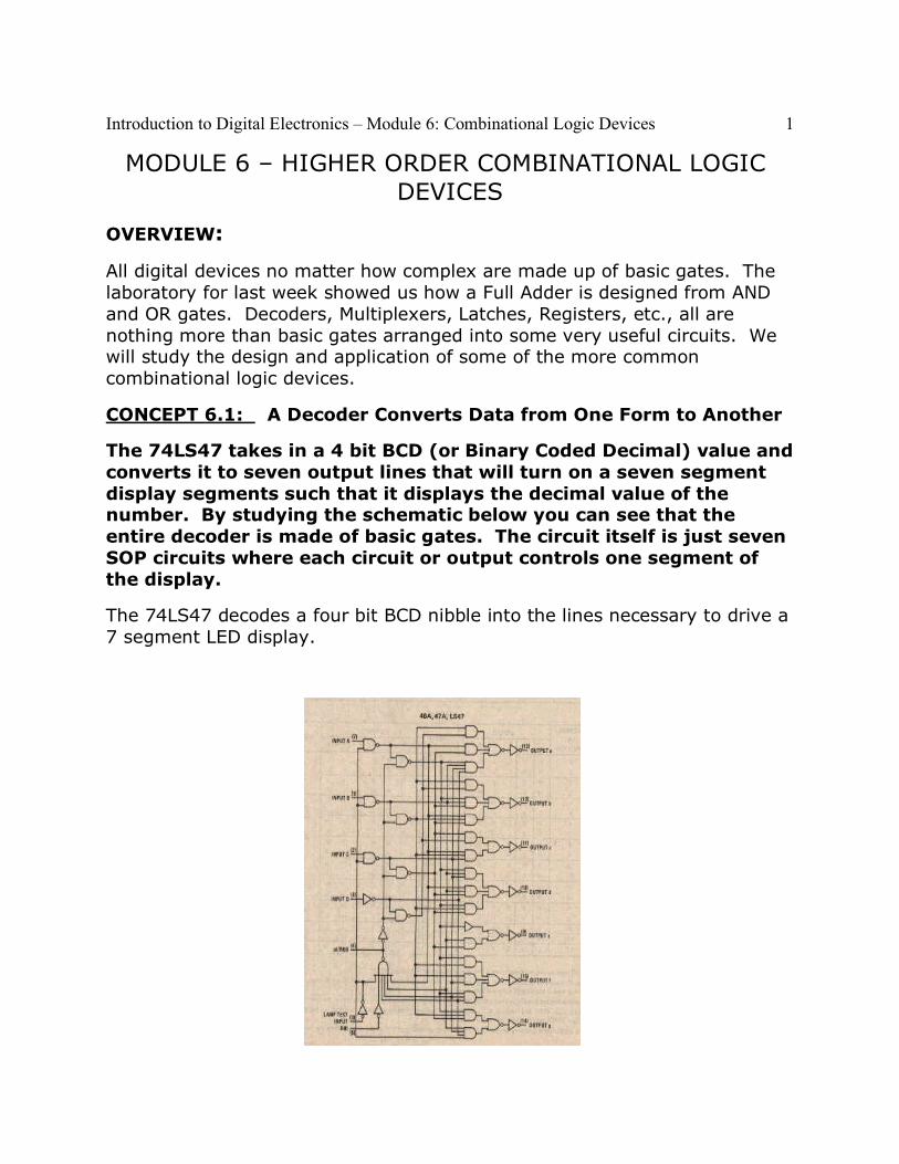
CONCEPT 6.1: A Decoder Converts Data from One Form to Another
The 74LS47 takes in a 4 bit BCD (or Binary Coded Decimal) value and converts it to seven output lines that will turn on a seven segment display segments such that it displays the decimal value of the number. By studying the schematic below you can see that the entire decoder is made of basic gates. The circuit itself is just seven SOP circuits where each circuit or output controls one segment of the display.
The 74LS47 decodes a four bit BCD nibble into the lines necessary to drive a 7 segment LED display.
Introduction to Digital Electronics – Module 6: Combinational Logic Devices 2
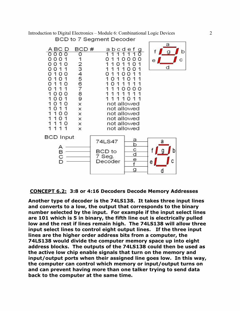
CONCEPT 6.2: 3:8 or 4:16 Decoders Decode Memory Addresses
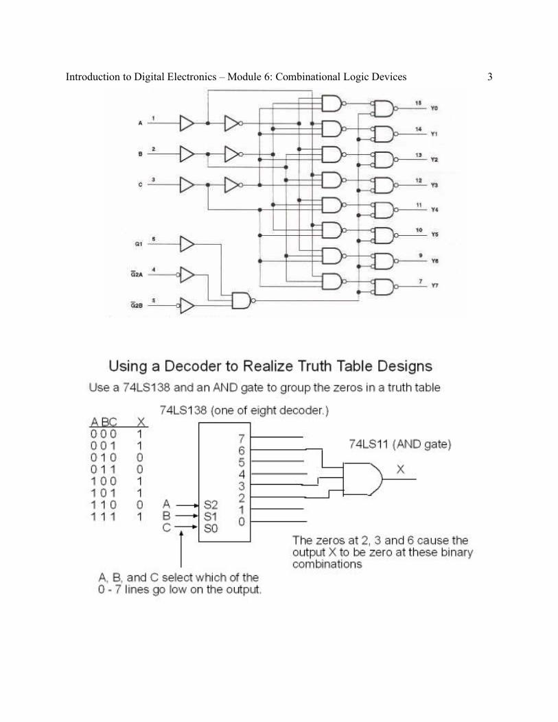
Another type of decoder is the 74LS138. It takes three input lines and converts to a low, the output that corresponds to the binary number selected by the input. For example if the input select lines are 101 which is 5 in binary, the fifth line out is electrically pulled low and the rest if lines remain high. The 74LS138 will allow three input select lines to control eight output lines. If the three input lines are the higher order address bits from a computer, the 74LS138 would divide the computer memory space up into eight address blocks. The outputs of the 74LS138 could then be used as the active low chip enable signals that turn on the memory and input/output ports when their assigned line goes low. In this way, the computer can control which memory or input/output turns on and can prevent having more than one talker trying to send data back to the computer at the same time.
Introduction to Digital Electronics – Module 6: Combinational Logic Devices 3
Introduction to Digital Electronics – Module 6: Combinational Logic Devices 4
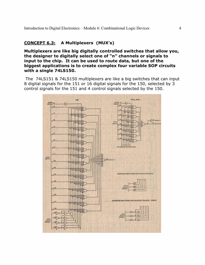
CONCEPT 6.3: A Multiplexers (MUX’s)
Multiplexers are like big digitally controlled switches that allow you, the designer to digitally select one of “n” channels or signals to input to the chip. It can be used to route data, but one of the biggest applications is to create complex four variable SOP circuits with a single 74LS150.
The 74LS151 & 74LS150 multiplexers are like a big switches that can input 8 digital signals for the 151 or 16 digital signals for the 150, selected by 3 control signals for the 151 and 4 control signals selected by the 150.
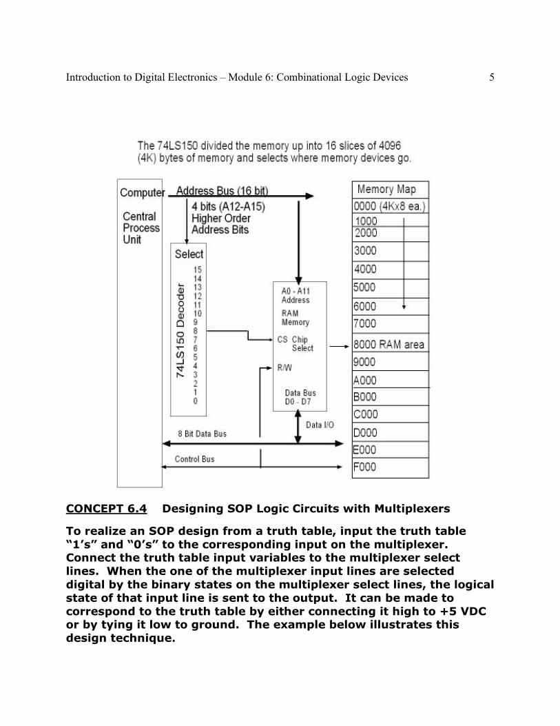
Introduction to Digital Electronics – Module 6: Combinational Logic Devices 5
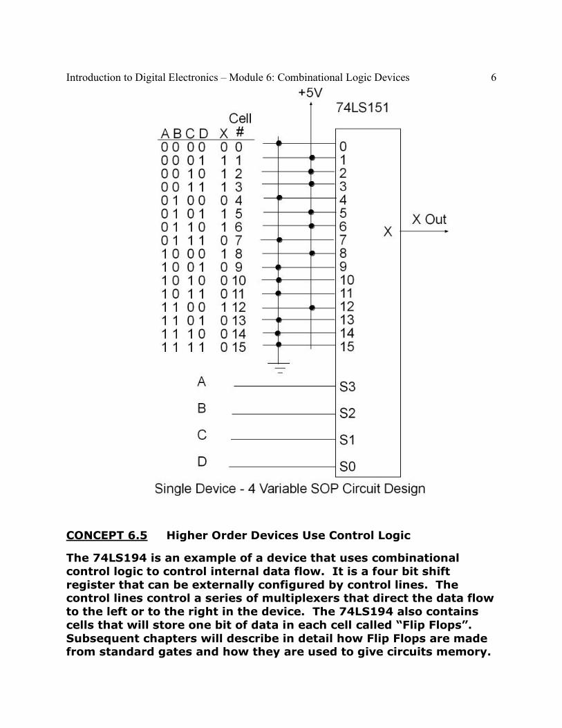
CONCEPT 6.4 Designing SOP Logic Circuits with Multiplexers
To realize an SOP design from a truth table, input the truth table “1’s” and “0’s” to the corresponding input on the multiplexer. Connect the truth table input variables to the multiplexer select lines. When the one of the multiplexer input lines are selected digital by the binary states on the multiplexer select lines, the logical state of that input line is sent to the output. It can be made to correspond to the truth table by either connecting it high to +5 VDC or by tying it low to ground. The example below illustrates this design technique.
Introduction to Digital Electronics – Module 6: Combinational Logic Devices 6
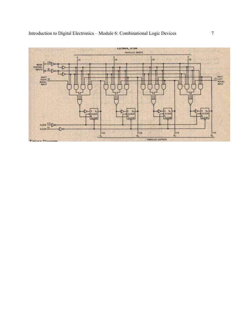
CONCEPT 6.5 Higher Order Devices Use Control Logic
The 74LS194 is an example of a device that uses combinational control logic to control internal data flow. It is a four bit shift register that can be externally configured by control lines. The control lines control a series of multiplexers that direct the data flow to the left or to the right in the device. The 74LS194 also contains cells that will store one bit of data in each cell called “Flip Flops”. Subsequent chapters will describe in detail how Flip Flops are made from standard gates and how they are used to give circuits memory.
Introduction to Digital Electronics – Module 6: Combinational Logic Devices 7