module 2 introduction to combinational logic circuits and
TRANSCRIPT

Digital system design 17EE35
Dept.EEE, ATMECE, Mysuru
MODULE 2
Introduction to Combinational Logic Circuits and Ad vanced Combinational Logic Circuits
Structure 2.1 Objevtive 2.2 Introduction 2.3 General approach 2.4 Decoders-BCD decoders, Encoders. 2.5 Digital multiplexers-using multiplexers as Boolean function generators & Design methods of
building blocks of combinational logics 2.6 Adders and Subtractors-Cascading full adders 2.7 Look ahead carry 2.8 Binary comparators. . 2.9 Outcome 2.10 Future Readings
2.1 Objevtive
• Ability to understand, analyze and design various combinational circuit. •
2.2 Introduction The complex combinational circuits can be designed using fundamental circuits, this fundamental circuits mean the we have considered half adder, full adder, the decoder. Now, we will read how the combinational circuits can be designed using another fundamental circuits called multiplexer 2.3 General approach Combinational Circuits A combinational circuit consists of logic gates whose outputs, at any time, are determined by combining the values of the inputs. A combinational circuit consists of logic gates whose outputs, at any time, are determined by combining the values of the inputs. For n input variables, there are 2 n possible binary input combinations. For n input variables, there are 2 n possible binary input combinations. For each binary combination of the input variables, there is one possible binary value on each output. For each binary combination of the input variables, there is one possible binary value on each output.
1. Design a combinational circuit that will multiply two two-bit binary values Solution: 1. input variables(A1,A0,B1,B0) output variables(P3,P2,P1,P0) Construct a truth table
26

Digital system design
Dept.EEE, ATMECE, Mysuru
The output SOP equations areP3=f(A1,A0,B1,B0)=∑(15)P2=f(A1,A0,B1,B0)=∑(10,11,14)P1=f(A1,A0,B1,B0)=∑(6,7,9,11,13,14)P0=f(A1,A0,B1,B0)=∑(5,7,13,15) The individually simplified equations areP3=A1A0B1B0 P2=A1A0’B1+A1B1B0’ P1=A1’A 0B1+A0B1B0’+AP0=A0B0
The output SOP equations are:
∑(15) ∑(10,11,14) ∑(6,7,9,11,13,14) ∑(5,7,13,15)
The individually simplified equations are
’+A 1B1’B 0+A1A0’B0
17EE35
27

Digital system design 17EE35
Dept.EEE, ATMECE, Mysuru
2.4 Decoders-BCD decoders, Encoders. A Decoder is a multiple input ,multiple output logic circuit.The block diagram of a decoder is as shown below.
The most commonly used decoder is a n –to 2n decoder which ha n inputs and 2n Output lines .
3-to-8 decoder logic diagram
28

Digital system design 17EE35
Dept.EEE, ATMECE, Mysuru
In this realization shown above the three inputs are assigned x0,x1,and x2, and the eight outputs are Z0 to Z7.
Function specifc decoders also exist which have less than 2n outputs . examples are 8421 code decoder also called BCD to decimal decoder. Decoders that drive seven segment displays also exist
Realization of boolean expression using Decoder and OR gate
We see from the above truth table that the output expressions corrwespond to a single minterm. Hence a n –to 2n decoder is a minterm generator. Thus by using OR gates in conjunction with a a n –to 2n decoder boolean function realization is possible.
P1: to realize the Boolean functions given below using decoders…
•F1=Σm(1,2,4,5)
•F2=Σm(1,5,7)
29

Digital system design 17EE35
Dept.EEE, ATMECE, Mysuru
P2: A 3-to-8 Decoder constructed
P3: Design a binary 3-bit adder with a 74xxx138 and NAND gates.
S = f (x , y , z)= ∑m (1, 2 , 4 , 7 ) , C f ( X , Y , Z ) ∑m (3 , 5 , 6 , 7 )
Encoder
It is a inverse of decoder having 2^n input and n output.
30

Digital system design 17EE35
Dept.EEE, ATMECE, Mysuru
P4: Decimal-to-BCD Encoder (74xxx147) Inputs Outputs
1 2 3 4 5 6 7 8 9 D C B A 1 0
x x x x x x x x
1 1 0
x x x x x x x
1 1 1 0
x x x x x x
1 1 1 1 0
x x x x x
1 1 1 1 1 0
x x x x
1 1 1 1 1 1 0
x x x
1 1 1 1 1 1 1 0
x x
1 1 1 1 1 1 1 1 0 x
1 1 1 1 1 1 1 1 1 0
priority encoder
Several possible events may occur in an industrial system, and you want to identify an event
and assign and transmit a code to the control unit based on some priority.
Inputs Outputs D3 D2 D1 D0 A1 A0 /V
0 0 0 0 1
0 0 0 1 X
0 0 1
X X
0 1
X X
+ 5 VU 1
H P R I/BCD
1
2
3
4
5
6
1
2
4
74 LS 147
31

Digital system design 17EE35
Dept.EEE, ATMECE, Mysuru
2.5 Digital multiplexers-using multiplexers as Boolean function generators. & Design methods of building blocks of combinational logics.
Multiplexers also called data selectors are another MSI devices with a wide range of applications in microprocessor and their peripherals design. The followind diagrams show the symbol and truth table for the 4-to –1 mux.
P1: 4-to-1 Line Multiplexer
32

Digital system design 17EE35
Dept.EEE, ATMECE, Mysuru
P2: Consider the function F(A,B,C,D)=∑(1,3,4,11,12,13,14,15)\
This function canbe implemented with an 8-to-1 line MUX (see Figure 7) A, B, and C are applied to the select inputs as follows: A ⇒ S2 , B ⇒ S1, C ⇒ S0
Demultiplexers
• Perform the opposite function of multiplexers
• Placing the value of a single data input onto one of the multiple data outputs
• Same implementation as decoder with enable
• Enable input of decoder serves as the data input for the demultiplexer
33

Digital system design 17EE35
Dept.EEE, ATMECE, Mysuru
P1: A 1-to-4 line Demux
The input E is directed to one of the outputs, as specified by the two select lines S1 and S0. D0 = E if S1S0 = 00 ⇒ D0 = S1’ S0’ E
D1 = E if S1S0 = 01 ⇒ D1 = S1’ S0 E
D2 = E if S1S0 = 10 ⇒ D2 = S1 S0’ E
D3 = E if S1S0 = 11 ⇒ D3 = S1 S0 E
A careful inspection of the Demux circuit shows that it is identical to a 2 to 4 decoder with enable input.
Table for 1-to-4 line demultiplexer
34

Digital system design
Dept.EEE, ATMECE, Mysuru
2.6 Adders and Subtractors-Consider adding two binary numbers together:
We see that the bit in the "two's" column is generated when the addition carried over. A halfadder is a circuit which adds two bits together and outputs the sum of those two bits. The halfadder has two outputs: sum andA+B/2, while carry is the result. This can be expressed as follows:
S= A xor B
C=AB
Full Adder:
Half-adders have a major limitation in that they cannot accept a carry bit from a previous stage, meaning that they cannot be chained togethbits of a half-adder can also represent the result A+B=3 as sum and carry both being high.
As such, the full-adder can accept three bits as an input. Commonly, one bit is referred to as the carry-in bit. Full adders can be cascaded to produce adders of any number of bits by daisychaining the carry of one output to the input of the next
The full-adder is usually shown as a single unit. The sum output is usually on the bottom on the block, and the carry-out output is on the left, so the devices can be chained together, most significant bit leftmost:
-Cascading full adders Consider adding two binary numbers together:
that the bit in the "two's" column is generated when the addition carried over. A halfadder is a circuit which adds two bits together and outputs the sum of those two bits. The half
and carry . Sum represents the remainder of theA+B/2, while carry is the result. This can be expressed as follows:
adders have a major limitation in that they cannot accept a carry bit from a previous stage, meaning that they cannot be chained together to add multi-bit numbers. However, the two output
adder can also represent the result A+B=3 as sum and carry both being high.
adder can accept three bits as an input. Commonly, one bit is referred to as the Full adders can be cascaded to produce adders of any number of bits by daisy
chaining the carry of one output to the input of the next
adder is usually shown as a single unit. The sum output is usually on the bottom on the out output is on the left, so the devices can be chained together, most
Logic Symbol of Full adder
17EE35
that the bit in the "two's" column is generated when the addition carried over. A half-adder is a circuit which adds two bits together and outputs the sum of those two bits. The half-
. Sum represents the remainder of the integer division
adders have a major limitation in that they cannot accept a carry bit from a previous stage, bit numbers. However, the two output
adder can also represent the result A+B=3 as sum and carry both being high.
adder can accept three bits as an input. Commonly, one bit is referred to as the Full adders can be cascaded to produce adders of any number of bits by daisy-
adder is usually shown as a single unit. The sum output is usually on the bottom on the out output is on the left, so the devices can be chained together, most
35

Digital system design 17EE35
Dept.EEE, ATMECE, Mysuru
Ripple Carry Adder:
A ripple carry adder is simply several full adders connected in a series so that the carry must propagate through every full adder before the addition is complete. Ripple carry adders require the least amount of hardware of all adders, but they are the slowest.
The following diagram shows a four-bit adder, which adds the numbers A[3:0] and B[3:0], as well as a carry input, together to produce S[3:0] and the carry output
Propagation Delay in Full Adders
Real logic gates do not react instantaneously to the inputs, and therefore digital circuits have a maximum speed. Usually, the delay through a digital circuit is measured in gate-delays, as this allows the delay of a design to be calculated for different devices. AND and OR gates have a nominal delay of 1 gate-delay, and XOR gates have a delay of 2, because they are really made up of a combination of ANDs and ORs.
A full adder block has the following worst case propagation delays:
• From Ai or Bi to Ci+1: 4 gate-delays (XOR → AND → OR) • From Ai or Bi to Si: 4 gate-delays (XOR → XOR) • From Ci to Ci+1: 2 gate-delays (AND → OR) • From Ci to Si: 2 gate-delays (XOR)
Because the carry-out of one stage is the next's input, the worst case propagation delay is then:
• 4 gate-delays from generating the first carry signal (A0/B0 → C1). • 2 gate-delays per intermediate stage (Ci → Ci+1).
36

Digital system design
Dept.EEE, ATMECE, Mysuru
• 2 gate-delays at the last stage to produ1 → Cn and Sn-1).
So for an n-bit adder, we have a total propagation delay,
This is linear in n, and for a 32This is rather slow, and restricts the word length in our device somewhat. We would like to find ways to speed it up.
2.7 Look ahead carry A fast method of adding numbers is called carrycarry signal to propagate stage by stage, causing a bottleneck. Instead it uses additional logic to expedite the propagation and generation of carry information, allowing fast addition at the expense of more hardware.
In a ripple adder, each stage compares the carrygenerates a carry-out signal Cfunctions.
The generate function, Gi, indicates whether that stage causes a carrygenerated if no carry-in signal exists. This occurs if both the addends contain a 1 in that bit:
Gi = A i .B i
The propagate function, Pi, indicates whether a carrythe stage. This occurs if either the addends have a 1 in
P i = A i + B i
Note that both these values can be calculated from the inputs in a constant time of a single gate delay. Now, the carry-out from a stage occurs if that stage generates a carry (carry-in and the stage propaga
delays at the last stage to produce both the sum and carry
bit adder, we have a total propagation delay, tp of:
, and for a 32-bit number, would take 66 cycles to complete the This is rather slow, and restricts the word length in our device somewhat. We would like to find
A fast method of adding numbers is called carry-lookahead. This method doesn't require the ropagate stage by stage, causing a bottleneck. Instead it uses additional logic to
expedite the propagation and generation of carry information, allowing fast addition at the
In a ripple adder, each stage compares the carry-in signal, Ci, with the inputsCi+1 accordingly. In a carry-lookahead adder, we define two new
, indicates whether that stage causes a carryin signal exists. This occurs if both the addends contain a 1 in that bit:
, indicates whether a carry-in to the stage is passed to the carrythe stage. This occurs if either the addends have a 1 in that bit
Note that both these values can be calculated from the inputs in a constant time of a single gate out from a stage occurs if that stage generates a carry (
in and the stage propagates the carry (Pi·Ci = 1)
17EE35
ce both the sum and carry-out outputs (Cn-
bit number, would take 66 cycles to complete the calculation. This is rather slow, and restricts the word length in our device somewhat. We would like to find
lookahead. This method doesn't require the ropagate stage by stage, causing a bottleneck. Instead it uses additional logic to
expedite the propagation and generation of carry information, allowing fast addition at the
, with the inputs Ai and Bi and lookahead adder, we define two new
, indicates whether that stage causes a carry-out signal Ci to be in signal exists. This occurs if both the addends contain a 1 in that bit:
in to the stage is passed to the carry-out for
Note that both these values can be calculated from the inputs in a constant time of a single gate out from a stage occurs if that stage generates a carry (Gi = 1) or there is a
37

Digital system design
Dept.EEE, ATMECE, Mysuru
C i+1 = A i B i + A i C i + B i C
C i+1 = A i B i + C i (A i + B i )
C i+1 = G i + P i C i
Truth table
Note that this does not require the carrywait for changes to ripple through the circuit. In fact, a given stage's carry signal can be computed once the propagate and generate signals are ready with only two more gate delays (one AND and one OR). Thus the carrytherefore so can the sum.
The S, P, and G signals are all generated by a circuit called a "partial full adder" (PFA), which is similar to a full adder.
For a slightly smaller circuit, the propagate signal can be taken as the output of the first gate instead of using a dedicated OR gate, because if both A and B are asserted, the generate signal will force a carry. However, this simplifiaction means that the propagate signal will take two gate delays to produce, rather than just one.
C i
Note that this does not require the carry-out signals from the previous stages, so we don't have to ripple through the circuit. In fact, a given stage's carry signal can be
computed once the propagate and generate signals are ready with only two more gate delays (one AND and one OR). Thus the carry-out for a given stage can be calculated in constant tim
signals are all generated by a circuit called a "partial full adder" (PFA), which is
For a slightly smaller circuit, the propagate signal can be taken as the output of the first gate instead of using a dedicated OR gate, because if both A and B are asserted, the generate signal will force a carry. However, this simplifiaction means that the propagate signal will take two gate delays to produce, rather than just one.
17EE35
out signals from the previous stages, so we don't have to ripple through the circuit. In fact, a given stage's carry signal can be
computed once the propagate and generate signals are ready with only two more gate delays (one out for a given stage can be calculated in constant time, and
signals are all generated by a circuit called a "partial full adder" (PFA), which is
For a slightly smaller circuit, the propagate signal can be taken as the output of the first XOR gate instead of using a dedicated OR gate, because if both A and B are asserted, the generate signal will force a carry. However, this simplifiaction means that the propagate signal will take
38

Digital system design
Dept.EEE, ATMECE, Mysuru
A carry lookahead adder then containspropagate and generate signals:
Two numbers can therefore be added in constant time, O(1), of just 6 gate delays, regardless of the length, n of the numbers. However, thislogic gates are available with a limited number of inputs, trees will need to be constructed to compute these, and the overall computation time is logarithmic, O(ln(better than the linear time for ripple adders.
2.8 Binary comparators Another common and very useful combinational logic circuit is that of theComparator circuit. Digital or Binary Comparators are made up from standard AND, NOR and NOTterminals and produce an output depending upon the condition of those inputs.
Another common and very useful combinational logic circuit is that of theComparator circuit. Digital or Binary Comparators are madstandard AND, NOR and NOTterminals and produce an output depending upon the condition of those inputs.
For example, along with being able to add and subtract binary numbers we need compare them and determine whether the value of inputto the value at input B etc. The digital comparator accomplishes this using several logic gates that operate on the principles ofComparator available and these are.
okahead adder then contains n PFAs and the logic to produce carries from the stage propagate and generate signals:
Two numbers can therefore be added in constant time, O(1), of just 6 gate delays, regardless of of the numbers. However, this requires AND and OR gates with up to
logic gates are available with a limited number of inputs, trees will need to be constructed to compute these, and the overall computation time is logarithmic, O(ln(n)), which is still much
linear time for ripple adders.
Another common and very useful combinational logic circuit is that of the circuit. Digital or Binary Comparators are made up from
NOT gates that compare the digital signals present at their input terminals and produce an output depending upon the condition of those inputs.
Another common and very useful combinational logic circuit is that of the circuit. Digital or Binary Comparators are made up from
NOT gates that compare the digital signals present at their input terminals and produce an output depending upon the condition of those inputs.
For example, along with being able to add and subtract binary numbers we need compare them and determine whether the value of input A is greater than, smaller than or equal
etc. The digital comparator accomplishes this using several logic gates that operate on the principles of Boolean Algebra. There are two main types of
available and these are.
17EE35
PFAs and the logic to produce carries from the stage
Two numbers can therefore be added in constant time, O(1), of just 6 gate delays, regardless of requires AND and OR gates with up to n inputs. If
logic gates are available with a limited number of inputs, trees will need to be constructed to )), which is still much
Digital
digital signals present at their input terminals and produce an output depending upon the condition of those inputs.
Digital
gates that compare the digital signals present at their input terminals and produce an output depending upon the condition of those inputs.
For example, along with being able to add and subtract binary numbers we need to be able to is greater than, smaller than or equal
etc. The digital comparator accomplishes this using several logic gates There are two main types of Digital
39

Digital system design 17EE35
Dept.EEE, ATMECE, Mysuru
• 1. Identity Comparator – an Identity Comparator is a digital comparator that has only one output terminal for when A = B either “HIGH” A = B = 1 or “LOW” A = B = 0
• 2. Magnitude Comparator – a Magnitude Comparator is a digital comparator which has three output terminals, one each for equality, A = B greater than, A > B and less than A < B
The purpose of a Digital Comparator is to compare a set of variables or unknown numbers, for example A (A1, A2, A3, …. An, etc) against that of a constant or unknown value such as B (B1, B2, B3, …. Bn, etc) and produce an output condition or flag depending upon the result of the comparison. For example, a magnitude comparator of two 1-bits, (A and B) inputs would produce the following three output conditions when compared to each other.
Which means: A is greater than B, A is equal to B, and A is less than B
This is useful if we want to compare two variables and want to produce an output when any of the above three conditions are achieved. For example, produce an output from a counter when a certain count number is reached. Consider the simple 1-bit comparator below.
1-bit Digital Comparator Circuit
Then the operation of a 1-bit digital comparator is given in the following Truth Table.
Digital Comparator Truth Table
Inputs Outputs
B A A > B A = B A < B
0 0 0 1 0
0 1 1 0 0
40

Digital system design 17EE35
Dept.EEE, ATMECE, Mysuru
1 0 0 0 1
1 1 0 1 0
You may notice two distinct features about the comparator from the above truth table. Firstly, the circuit does not distinguish between either two “0” or two “1”‘s as an output A = B is produced when they are both equal, either A = B = “0” or A = B = “1”. Secondly, the output condition for A = B resembles that of a commonly available logic gate, the Exclusive-NOR or Ex-NOR function (equivalence) on each of the n-bits giving: Q = A ⊕ B
Digital comparators actually use Exclusive-NOR gates within their design for comparing their respective pairs of bits. When we are comparing two binary or BCD values or variables against each other, we are comparing the “magnitude” of these values, a logic “0” against a logic “1” which is where the term Magnitude Comparator comes from.
As well as comparing individual bits, we can design larger bit comparators by cascading together n of these and produce a n-bit comparator just as we did for the n-bit adder in the previous tutorial. Multi-bit comparators can be constructed to compare whole binary or BCD words to produce an output if one word is larger, equal to or less than the other.
A very good example of this is the 4-bit Magnitude Comparator. Here, two 4-bit words (“nibbles”) are compared to each other to produce the relevant output with one word connected to inputs A and the other to be compared against connected to input B as shown below.
4-bit Magnitude Comparator
Some commercially available digital comparators such as the TTL 74LS85 or CMOS 4063 4-bit magnitude comparator have additional input terminals that allow more individual comparators to be “cascaded” together to compare words larger than 4-bits with magnitude comparators of “n”-bits being produced. These cascading inputs are connected directly to the corresponding outputs of the previous comparator as shown to compare 8, 16 or even 32-bit words.
41

Digital system design 17EE35
Dept.EEE, ATMECE, Mysuru
8-bit Word Comparator
When comparing large binary or BCD numbers like the example above, to save time the comparator starts by comparing the highest-order bit (MSB) first. If equality exists, A = B then it compares the next lowest bit and so on until it reaches the lowest-order bit, (LSB). If equality still exists then the two numbers are defined as being equal.
If inequality is found, either A > B or A < B the relationship between the two numbers is determined and the comparison between any additional lower order bits stops. Digital Comparator are used widely in Analogue-to-Digital converters, (ADC) and Arithmetic Logic Units, (ALU) to perform a variety of arithmetic operations.
42

Digital system design 17EE35
Dept.EEE, ATMECE, Mysuru
2.9 Outcome • Can create a appropriate truth table from the description of combinational logic
function. • Able to design any logic circuit using MUX, DEMUX, encoders and decoders
based on the application such that the gates used in a circuits are reduced.
2.10 Future Readings
http://nptel.ac.in/courses/117105080/
https://www.youtube.com/watch?v=VnZLRrJYa2I
“Logic Design” by RD Sudhaker Samuel
“Digital Logic Applications and Design” by John M Yarbrough, 2011 edition.
43

Digital system design 17EE35
Dept.EEE, ATMECE, Mysuru
MODULE 2
Introduction to Combinational Logic Circuits and Ad vanced Combinational Logic Circuits
Structure 2.1 Objevtive 2.2 Introduction 2.3 General approach 2.4 Decoders-BCD decoders, Encoders. 2.5 Digital multiplexers-using multiplexers as Boolean function generators & Design methods of
building blocks of combinational logics 2.6 Adders and Subtractors-Cascading full adders 2.7 Look ahead carry 2.8 Binary comparators. . 2.9 Outcome 2.10 Future Readings
2.1 Objevtive
• Ability to understand, analyze and design various combinational circuit. •
2.2 Introduction The complex combinational circuits can be designed using fundamental circuits, this fundamental circuits mean the we have considered half adder, full adder, the decoder. Now, we will read how the combinational circuits can be designed using another fundamental circuits called multiplexer 2.3 General approach Combinational Circuits A combinational circuit consists of logic gates whose outputs, at any time, are determined by combining the values of the inputs. A combinational circuit consists of logic gates whose outputs, at any time, are determined by combining the values of the inputs. For n input variables, there are 2 n possible binary input combinations. For n input variables, there are 2 n possible binary input combinations. For each binary combination of the input variables, there is one possible binary value on each output. For each binary combination of the input variables, there is one possible binary value on each output.
1. Design a combinational circuit that will multiply two two-bit binary values Solution: 1. input variables(A1,A0,B1,B0) output variables(P3,P2,P1,P0) Construct a truth table
26

Digital system design
Dept.EEE, ATMECE, Mysuru
The output SOP equations areP3=f(A1,A0,B1,B0)=∑(15)P2=f(A1,A0,B1,B0)=∑(10,11,14)P1=f(A1,A0,B1,B0)=∑(6,7,9,11,13,14)P0=f(A1,A0,B1,B0)=∑(5,7,13,15) The individually simplified equations areP3=A1A0B1B0 P2=A1A0’B1+A1B1B0’ P1=A1’A 0B1+A0B1B0’+AP0=A0B0
The output SOP equations are:
∑(15) ∑(10,11,14) ∑(6,7,9,11,13,14) ∑(5,7,13,15)
The individually simplified equations are
’+A 1B1’B 0+A1A0’B0
17EE35
27

Digital system design 17EE35
Dept.EEE, ATMECE, Mysuru
2.4 Decoders-BCD decoders, Encoders. A Decoder is a multiple input ,multiple output logic circuit.The block diagram of a decoder is as shown below.
The most commonly used decoder is a n –to 2n decoder which ha n inputs and 2n Output lines .
3-to-8 decoder logic diagram
28

Digital system design 17EE35
Dept.EEE, ATMECE, Mysuru
In this realization shown above the three inputs are assigned x0,x1,and x2, and the eight outputs are Z0 to Z7.
Function specifc decoders also exist which have less than 2n outputs . examples are 8421 code decoder also called BCD to decimal decoder. Decoders that drive seven segment displays also exist
Realization of boolean expression using Decoder and OR gate
We see from the above truth table that the output expressions corrwespond to a single minterm. Hence a n –to 2n decoder is a minterm generator. Thus by using OR gates in conjunction with a a n –to 2n decoder boolean function realization is possible.
P1: to realize the Boolean functions given below using decoders…
•F1=Σm(1,2,4,5)
•F2=Σm(1,5,7)
29

Digital system design 17EE35
Dept.EEE, ATMECE, Mysuru
P2: A 3-to-8 Decoder constructed
P3: Design a binary 3-bit adder with a 74xxx138 and NAND gates.
S = f (x , y , z)= ∑m (1, 2 , 4 , 7 ) , C f ( X , Y , Z ) ∑m (3 , 5 , 6 , 7 )
Encoder
It is a inverse of decoder having 2^n input and n output.
30

Digital system design 17EE35
Dept.EEE, ATMECE, Mysuru
P4: Decimal-to-BCD Encoder (74xxx147) Inputs Outputs
1 2 3 4 5 6 7 8 9 D C B A 1 0
x x x x x x x x
1 1 0
x x x x x x x
1 1 1 0
x x x x x x
1 1 1 1 0
x x x x x
1 1 1 1 1 0
x x x x
1 1 1 1 1 1 0
x x x
1 1 1 1 1 1 1 0
x x
1 1 1 1 1 1 1 1 0 x
1 1 1 1 1 1 1 1 1 0
priority encoder
Several possible events may occur in an industrial system, and you want to identify an event
and assign and transmit a code to the control unit based on some priority.
Inputs Outputs D3 D2 D1 D0 A1 A0 /V
0 0 0 0 1
0 0 0 1 X
0 0 1
X X
0 1
X X
+ 5 VU 1
H P R I/BCD
1
2
3
4
5
6
1
2
4
74 LS 147
31

Digital system design 17EE35
Dept.EEE, ATMECE, Mysuru
2.5 Digital multiplexers-using multiplexers as Boolean function generators. & Design methods of building blocks of combinational logics.
Multiplexers also called data selectors are another MSI devices with a wide range of applications in microprocessor and their peripherals design. The followind diagrams show the symbol and truth table for the 4-to –1 mux.
P1: 4-to-1 Line Multiplexer
32

Digital system design 17EE35
Dept.EEE, ATMECE, Mysuru
P2: Consider the function F(A,B,C,D)=∑(1,3,4,11,12,13,14,15)\
This function canbe implemented with an 8-to-1 line MUX (see Figure 7) A, B, and C are applied to the select inputs as follows: A ⇒ S2 , B ⇒ S1, C ⇒ S0
Demultiplexers
• Perform the opposite function of multiplexers
• Placing the value of a single data input onto one of the multiple data outputs
• Same implementation as decoder with enable
• Enable input of decoder serves as the data input for the demultiplexer
33

Digital system design 17EE35
Dept.EEE, ATMECE, Mysuru
P1: A 1-to-4 line Demux
The input E is directed to one of the outputs, as specified by the two select lines S1 and S0. D0 = E if S1S0 = 00 ⇒ D0 = S1’ S0’ E
D1 = E if S1S0 = 01 ⇒ D1 = S1’ S0 E
D2 = E if S1S0 = 10 ⇒ D2 = S1 S0’ E
D3 = E if S1S0 = 11 ⇒ D3 = S1 S0 E
A careful inspection of the Demux circuit shows that it is identical to a 2 to 4 decoder with enable input.
Table for 1-to-4 line demultiplexer
34

Digital system design
Dept.EEE, ATMECE, Mysuru
2.6 Adders and Subtractors-Consider adding two binary numbers together:
We see that the bit in the "two's" column is generated when the addition carried over. A halfadder is a circuit which adds two bits together and outputs the sum of those two bits. The halfadder has two outputs: sum andA+B/2, while carry is the result. This can be expressed as follows:
S= A xor B
C=AB
Full Adder:
Half-adders have a major limitation in that they cannot accept a carry bit from a previous stage, meaning that they cannot be chained togethbits of a half-adder can also represent the result A+B=3 as sum and carry both being high.
As such, the full-adder can accept three bits as an input. Commonly, one bit is referred to as the carry-in bit. Full adders can be cascaded to produce adders of any number of bits by daisychaining the carry of one output to the input of the next
The full-adder is usually shown as a single unit. The sum output is usually on the bottom on the block, and the carry-out output is on the left, so the devices can be chained together, most significant bit leftmost:
-Cascading full adders Consider adding two binary numbers together:
that the bit in the "two's" column is generated when the addition carried over. A halfadder is a circuit which adds two bits together and outputs the sum of those two bits. The half
and carry . Sum represents the remainder of theA+B/2, while carry is the result. This can be expressed as follows:
adders have a major limitation in that they cannot accept a carry bit from a previous stage, meaning that they cannot be chained together to add multi-bit numbers. However, the two output
adder can also represent the result A+B=3 as sum and carry both being high.
adder can accept three bits as an input. Commonly, one bit is referred to as the Full adders can be cascaded to produce adders of any number of bits by daisy
chaining the carry of one output to the input of the next
adder is usually shown as a single unit. The sum output is usually on the bottom on the out output is on the left, so the devices can be chained together, most
Logic Symbol of Full adder
17EE35
that the bit in the "two's" column is generated when the addition carried over. A half-adder is a circuit which adds two bits together and outputs the sum of those two bits. The half-
. Sum represents the remainder of the integer division
adders have a major limitation in that they cannot accept a carry bit from a previous stage, bit numbers. However, the two output
adder can also represent the result A+B=3 as sum and carry both being high.
adder can accept three bits as an input. Commonly, one bit is referred to as the Full adders can be cascaded to produce adders of any number of bits by daisy-
adder is usually shown as a single unit. The sum output is usually on the bottom on the out output is on the left, so the devices can be chained together, most
35

Digital system design 17EE35
Dept.EEE, ATMECE, Mysuru
Ripple Carry Adder:
A ripple carry adder is simply several full adders connected in a series so that the carry must propagate through every full adder before the addition is complete. Ripple carry adders require the least amount of hardware of all adders, but they are the slowest.
The following diagram shows a four-bit adder, which adds the numbers A[3:0] and B[3:0], as well as a carry input, together to produce S[3:0] and the carry output
Propagation Delay in Full Adders
Real logic gates do not react instantaneously to the inputs, and therefore digital circuits have a maximum speed. Usually, the delay through a digital circuit is measured in gate-delays, as this allows the delay of a design to be calculated for different devices. AND and OR gates have a nominal delay of 1 gate-delay, and XOR gates have a delay of 2, because they are really made up of a combination of ANDs and ORs.
A full adder block has the following worst case propagation delays:
• From Ai or Bi to Ci+1: 4 gate-delays (XOR → AND → OR) • From Ai or Bi to Si: 4 gate-delays (XOR → XOR) • From Ci to Ci+1: 2 gate-delays (AND → OR) • From Ci to Si: 2 gate-delays (XOR)
Because the carry-out of one stage is the next's input, the worst case propagation delay is then:
• 4 gate-delays from generating the first carry signal (A0/B0 → C1). • 2 gate-delays per intermediate stage (Ci → Ci+1).
36

Digital system design
Dept.EEE, ATMECE, Mysuru
• 2 gate-delays at the last stage to produ1 → Cn and Sn-1).
So for an n-bit adder, we have a total propagation delay,
This is linear in n, and for a 32This is rather slow, and restricts the word length in our device somewhat. We would like to find ways to speed it up.
2.7 Look ahead carry A fast method of adding numbers is called carrycarry signal to propagate stage by stage, causing a bottleneck. Instead it uses additional logic to expedite the propagation and generation of carry information, allowing fast addition at the expense of more hardware.
In a ripple adder, each stage compares the carrygenerates a carry-out signal Cfunctions.
The generate function, Gi, indicates whether that stage causes a carrygenerated if no carry-in signal exists. This occurs if both the addends contain a 1 in that bit:
Gi = A i .B i
The propagate function, Pi, indicates whether a carrythe stage. This occurs if either the addends have a 1 in
P i = A i + B i
Note that both these values can be calculated from the inputs in a constant time of a single gate delay. Now, the carry-out from a stage occurs if that stage generates a carry (carry-in and the stage propaga
delays at the last stage to produce both the sum and carry
bit adder, we have a total propagation delay, tp of:
, and for a 32-bit number, would take 66 cycles to complete the This is rather slow, and restricts the word length in our device somewhat. We would like to find
A fast method of adding numbers is called carry-lookahead. This method doesn't require the ropagate stage by stage, causing a bottleneck. Instead it uses additional logic to
expedite the propagation and generation of carry information, allowing fast addition at the
In a ripple adder, each stage compares the carry-in signal, Ci, with the inputsCi+1 accordingly. In a carry-lookahead adder, we define two new
, indicates whether that stage causes a carryin signal exists. This occurs if both the addends contain a 1 in that bit:
, indicates whether a carry-in to the stage is passed to the carrythe stage. This occurs if either the addends have a 1 in that bit
Note that both these values can be calculated from the inputs in a constant time of a single gate out from a stage occurs if that stage generates a carry (
in and the stage propagates the carry (Pi·Ci = 1)
17EE35
ce both the sum and carry-out outputs (Cn-
bit number, would take 66 cycles to complete the calculation. This is rather slow, and restricts the word length in our device somewhat. We would like to find
lookahead. This method doesn't require the ropagate stage by stage, causing a bottleneck. Instead it uses additional logic to
expedite the propagation and generation of carry information, allowing fast addition at the
, with the inputs Ai and Bi and lookahead adder, we define two new
, indicates whether that stage causes a carry-out signal Ci to be in signal exists. This occurs if both the addends contain a 1 in that bit:
in to the stage is passed to the carry-out for
Note that both these values can be calculated from the inputs in a constant time of a single gate out from a stage occurs if that stage generates a carry (Gi = 1) or there is a
37

Digital system design
Dept.EEE, ATMECE, Mysuru
C i+1 = A i B i + A i C i + B i C
C i+1 = A i B i + C i (A i + B i )
C i+1 = G i + P i C i
Truth table
Note that this does not require the carrywait for changes to ripple through the circuit. In fact, a given stage's carry signal can be computed once the propagate and generate signals are ready with only two more gate delays (one AND and one OR). Thus the carrytherefore so can the sum.
The S, P, and G signals are all generated by a circuit called a "partial full adder" (PFA), which is similar to a full adder.
For a slightly smaller circuit, the propagate signal can be taken as the output of the first gate instead of using a dedicated OR gate, because if both A and B are asserted, the generate signal will force a carry. However, this simplifiaction means that the propagate signal will take two gate delays to produce, rather than just one.
C i
Note that this does not require the carry-out signals from the previous stages, so we don't have to ripple through the circuit. In fact, a given stage's carry signal can be
computed once the propagate and generate signals are ready with only two more gate delays (one AND and one OR). Thus the carry-out for a given stage can be calculated in constant tim
signals are all generated by a circuit called a "partial full adder" (PFA), which is
For a slightly smaller circuit, the propagate signal can be taken as the output of the first gate instead of using a dedicated OR gate, because if both A and B are asserted, the generate signal will force a carry. However, this simplifiaction means that the propagate signal will take two gate delays to produce, rather than just one.
17EE35
out signals from the previous stages, so we don't have to ripple through the circuit. In fact, a given stage's carry signal can be
computed once the propagate and generate signals are ready with only two more gate delays (one out for a given stage can be calculated in constant time, and
signals are all generated by a circuit called a "partial full adder" (PFA), which is
For a slightly smaller circuit, the propagate signal can be taken as the output of the first XOR gate instead of using a dedicated OR gate, because if both A and B are asserted, the generate signal will force a carry. However, this simplifiaction means that the propagate signal will take
38

Digital system design
Dept.EEE, ATMECE, Mysuru
A carry lookahead adder then containspropagate and generate signals:
Two numbers can therefore be added in constant time, O(1), of just 6 gate delays, regardless of the length, n of the numbers. However, thislogic gates are available with a limited number of inputs, trees will need to be constructed to compute these, and the overall computation time is logarithmic, O(ln(better than the linear time for ripple adders.
2.8 Binary comparators Another common and very useful combinational logic circuit is that of theComparator circuit. Digital or Binary Comparators are made up from standard AND, NOR and NOTterminals and produce an output depending upon the condition of those inputs.
Another common and very useful combinational logic circuit is that of theComparator circuit. Digital or Binary Comparators are madstandard AND, NOR and NOTterminals and produce an output depending upon the condition of those inputs.
For example, along with being able to add and subtract binary numbers we need compare them and determine whether the value of inputto the value at input B etc. The digital comparator accomplishes this using several logic gates that operate on the principles ofComparator available and these are.
okahead adder then contains n PFAs and the logic to produce carries from the stage propagate and generate signals:
Two numbers can therefore be added in constant time, O(1), of just 6 gate delays, regardless of of the numbers. However, this requires AND and OR gates with up to
logic gates are available with a limited number of inputs, trees will need to be constructed to compute these, and the overall computation time is logarithmic, O(ln(n)), which is still much
linear time for ripple adders.
Another common and very useful combinational logic circuit is that of the circuit. Digital or Binary Comparators are made up from
NOT gates that compare the digital signals present at their input terminals and produce an output depending upon the condition of those inputs.
Another common and very useful combinational logic circuit is that of the circuit. Digital or Binary Comparators are made up from
NOT gates that compare the digital signals present at their input terminals and produce an output depending upon the condition of those inputs.
For example, along with being able to add and subtract binary numbers we need compare them and determine whether the value of input A is greater than, smaller than or equal
etc. The digital comparator accomplishes this using several logic gates that operate on the principles of Boolean Algebra. There are two main types of
available and these are.
17EE35
PFAs and the logic to produce carries from the stage
Two numbers can therefore be added in constant time, O(1), of just 6 gate delays, regardless of requires AND and OR gates with up to n inputs. If
logic gates are available with a limited number of inputs, trees will need to be constructed to )), which is still much
Digital
digital signals present at their input terminals and produce an output depending upon the condition of those inputs.
Digital
gates that compare the digital signals present at their input terminals and produce an output depending upon the condition of those inputs.
For example, along with being able to add and subtract binary numbers we need to be able to is greater than, smaller than or equal
etc. The digital comparator accomplishes this using several logic gates There are two main types of Digital
39

Digital system design 17EE35
Dept.EEE, ATMECE, Mysuru
• 1. Identity Comparator – an Identity Comparator is a digital comparator that has only one output terminal for when A = B either “HIGH” A = B = 1 or “LOW” A = B = 0
• 2. Magnitude Comparator – a Magnitude Comparator is a digital comparator which has three output terminals, one each for equality, A = B greater than, A > B and less than A < B
The purpose of a Digital Comparator is to compare a set of variables or unknown numbers, for example A (A1, A2, A3, …. An, etc) against that of a constant or unknown value such as B (B1, B2, B3, …. Bn, etc) and produce an output condition or flag depending upon the result of the comparison. For example, a magnitude comparator of two 1-bits, (A and B) inputs would produce the following three output conditions when compared to each other.
Which means: A is greater than B, A is equal to B, and A is less than B
This is useful if we want to compare two variables and want to produce an output when any of the above three conditions are achieved. For example, produce an output from a counter when a certain count number is reached. Consider the simple 1-bit comparator below.
1-bit Digital Comparator Circuit
Then the operation of a 1-bit digital comparator is given in the following Truth Table.
Digital Comparator Truth Table
Inputs Outputs
B A A > B A = B A < B
0 0 0 1 0
0 1 1 0 0
40

Digital system design 17EE35
Dept.EEE, ATMECE, Mysuru
1 0 0 0 1
1 1 0 1 0
You may notice two distinct features about the comparator from the above truth table. Firstly, the circuit does not distinguish between either two “0” or two “1”‘s as an output A = B is produced when they are both equal, either A = B = “0” or A = B = “1”. Secondly, the output condition for A = B resembles that of a commonly available logic gate, the Exclusive-NOR or Ex-NOR function (equivalence) on each of the n-bits giving: Q = A ⊕ B
Digital comparators actually use Exclusive-NOR gates within their design for comparing their respective pairs of bits. When we are comparing two binary or BCD values or variables against each other, we are comparing the “magnitude” of these values, a logic “0” against a logic “1” which is where the term Magnitude Comparator comes from.
As well as comparing individual bits, we can design larger bit comparators by cascading together n of these and produce a n-bit comparator just as we did for the n-bit adder in the previous tutorial. Multi-bit comparators can be constructed to compare whole binary or BCD words to produce an output if one word is larger, equal to or less than the other.
A very good example of this is the 4-bit Magnitude Comparator. Here, two 4-bit words (“nibbles”) are compared to each other to produce the relevant output with one word connected to inputs A and the other to be compared against connected to input B as shown below.
4-bit Magnitude Comparator
Some commercially available digital comparators such as the TTL 74LS85 or CMOS 4063 4-bit magnitude comparator have additional input terminals that allow more individual comparators to be “cascaded” together to compare words larger than 4-bits with magnitude comparators of “n”-bits being produced. These cascading inputs are connected directly to the corresponding outputs of the previous comparator as shown to compare 8, 16 or even 32-bit words.
41

Digital system design 17EE35
Dept.EEE, ATMECE, Mysuru
8-bit Word Comparator
When comparing large binary or BCD numbers like the example above, to save time the comparator starts by comparing the highest-order bit (MSB) first. If equality exists, A = B then it compares the next lowest bit and so on until it reaches the lowest-order bit, (LSB). If equality still exists then the two numbers are defined as being equal.
If inequality is found, either A > B or A < B the relationship between the two numbers is determined and the comparison between any additional lower order bits stops. Digital Comparator are used widely in Analogue-to-Digital converters, (ADC) and Arithmetic Logic Units, (ALU) to perform a variety of arithmetic operations.
42

Digital system design 17EE35
Dept.EEE, ATMECE, Mysuru
2.9 Outcome • Can create a appropriate truth table from the description of combinational logic
function. • Able to design any logic circuit using MUX, DEMUX, encoders and decoders
based on the application such that the gates used in a circuits are reduced.
2.10 Future Readings
http://nptel.ac.in/courses/117105080/
https://www.youtube.com/watch?v=VnZLRrJYa2I
“Logic Design” by RD Sudhaker Samuel
“Digital Logic Applications and Design” by John M Yarbrough, 2011 edition.
43

Digital System Design 17EE35
Dept. EEE, ATMECE, Mysuru
MODULE 3
Flip Flops and Characteristic Equation Structure 3.1 Objevtive 3.2 Introduction 3.3 Basic Bistable element 3.4 Latches, SR latch, 3.5 Application of SR latch,-A Switch debouncer. 3.6 The gated SR latch. 3.7 The gated D Latch, 3.8 The Master-Slave Flip-Flops (Pulse-Triggered Flip-Flops): The master-slave SR Flip-Flops,
The master-slave JK Flip-Flop, 3.9 Edge Triggered Flip-flop: The Positive Edge-Triggered D Flip-Flop, Negative-Edge
Triggered D Flip-Flop - Characteristic equations. 3.10 Registers, 3.11 Counters-Binary Ripple Counter, Synchronous Binary counters, Counters based on Shift
Registers, 3.12 Design of a Synchronous counters, Design of a Synchronous Mod-N counters using clocked
JK FlipFlops 3.13 Design of a Synchronous Mod-N counter using clocked D, T, or SR Flip-Flops. 3.14 Outcome 3.15 Future Readings 3.1 Objevtive
• To know different between latches and flip flops • Data storage elements • Designing of flip flops • Design of synchronous Mod N for all the flip flops
3.2 Introduction
Logic circuit is divided into two types.
1. Combinational Logic Circuit
2. Sequential Logic Circuit
Definition :
1. Combinational Logic Circuit :
The circuit in which outputs depends on only present value of inputs. So it is possible to describe each output as function of inputs by using Boolean expression. No memory element involved. No clock input. Circuit is implemented by using logic gates. The propagation delay depends on, delay of logic gates. Examples of combinational logic circuits are : full adder, subtractor, decoder, codeconverter, multiplexers etc.
44

Digital System Design 17EE35
Dept. EEE, ATMECE, Mysuru
2. Sequential Circuits :
Sequential Circuit is the logic circuit in which output depends on present value of inputs at that instant and past history of circuit i.e. previous output. The past output is stored by using memory device. The internal data stored in circuit is called as state. The clock is required for synchronization. The delay depends on propagation delay of circuit and clock frequency. The examples are flip-flops, registers, counters etc.
3.3 Basic Bistable element
o Flip-Flop is Bistable element.
o It consist of two cross coupled NOT Gates.
o It has two stable states.
o Q and Q are two outputs complement of each other.
o The data stored 1 or 0 in basic bistable element is state of flip-flop.
o 1 – State is set condition for flip-flop.
o 0 – State is reset / clear for flip-flop.
o It stores 1 or 0 state as long power is ON.
Combinational
Logic Circuit
inputs outputs
Combinational
Logic Circuit
inputs outputs
Memory Device
45

Digital System Design
Dept. EEE, ATMECE, Mysuru
3.4 Latches, SR latch
S-R Latch : Set-reset Flip-Flop
� Latch is a storage device by using Flip
� Latch can be controlled by direct inputs.
� Latch outputs can be controlled by clock or enable input.
� Q and Q are present state for output.
� Q+ and Q+ are next states for output.
� The function table / Truth table gives relation between inputs and outputs.
� The S=R=1 condition is not allowed in SR FF as output is unpredictable.
3.5 Application of SR latch-
� A switch debouncer
Flop
Latch is a storage device by using Flip-Flop.
controlled by direct inputs.
Latch outputs can be controlled by clock or enable input.
Q are present state for output.
are next states for output.
The function table / Truth table gives relation between inputs and outputs.
ition is not allowed in SR FF as output is unpredictable.
A Switch debouncer.
17EE35
The function table / Truth table gives relation between inputs and outputs.
ition is not allowed in SR FF as output is unpredictable.
46

Digital System Design
Dept. EEE, ATMECE, Mysuru
� Bouncing problem with Push button switch.
� Debouncing action.
� SR Flip-Flop as switch debouncer.
3.6 The gated SR latch. Characteristic equations,
� Enable input C is clock input.
� C=1, Output changes as per input condition.
� C=0, No change of state.
� S=1, R=0 is set condition for Flip
� S=0, R=1 is reset condition for Flip
� S=R=1 is ambiguous state, not allowed.
3.7 The gated D Latch Characteristic equations,
Bouncing problem with Push button switch.
Flop as switch debouncer.
Characteristic equations,
Enable input C is clock input.
C=1, Output changes as per input condition.
S=1, R=0 is set condition for Flip-flop.
S=0, R=1 is reset condition for Flip-flop.
S=R=1 is ambiguous state, not allowed.
Characteristic equations,
17EE35
47

Digital System Design
Dept. EEE, ATMECE, Mysuru
� D Flip-Flop is Data Flip
� D Flip-Flop stores 1 or 0.
� R input is complement of S.
� Only one D input is present.
� D Flip-Flop is a storage device used in register.
3.8 The Master-Slave Flip-Flops (PulseFlops, The master-slave JK Flip
� Two SR Flip-Flop, 1st
� Master Flip-Flop is positive edge triggered.
� Slave Flip-Flop is negative edge triggered.
Flop is Data Flip-Flop.
Flop stores 1 or 0.
R input is complement of S.
Only one D input is present.
Flop is a storage device used in register.
Flops (Pulse-Triggered Flip-Flops): The masterslave JK Flip-Flop Characteristic equations,
is Master and 2nd is slave.
Flop is positive edge triggered.
Flop is negative edge triggered.
17EE35
Flops): The master-slave SR Flip-
48
Digital System Design
Dept. EEE, ATMECE, Mysuru
� Slave follows master output.
� The output is delayed.
Master slave JK Flip-Flop Characteristic equations,
� In SR Flip-Flop the input combination S=R=1 is not allowed.
� JK FF is modified version of SR FF.
� Due to feedback from slave FF output to master, J=K=1 is allowed.
� J=K=1, toggle, action in FF.This finds application in counter.
Slave follows master output.
The output is delayed.
Characteristic equations,
Flop the input combination S=R=1 is not allowed.
JK FF is modified version of SR FF.
Due to feedback from slave FF output to master, J=K=1 is allowed.
J=K=1, toggle, action in FF. This finds application in counter.
17EE35
Due to feedback from slave FF output to master, J=K=1 is allowed.
49

Digital System Design
Dept. EEE, ATMECE, Mysuru
3.9 Edge Triggered Flip-flop: The Positive EdgeTriggered D Flip-Flop. Characteristic equations,
Positive Edge Triggered D Flip
� When C=0, the output of AND Gate 2 & 3 is equal to 1.
� If C=1, D=1, the output of AND Gate 2 is 0 and 3 is 1.
3.10 Registers
� Register is a group of Flip
� It stores binary information 0 or 1.
� It is capable of moving data left or right with clock pulse.
� Registers are classified as
• Serial-in Serial
• Serial-in parallel
• Parallel-in Serial
S R 1, No Change= =
S R 1, Q =1 and = =0,
flop: The Positive Edge-Triggered D Flip-Characteristic equations,
Positive Edge Triggered D Flip-Flop
When C=0, the output of AND Gate 2 & 3 is equal to 1.
If C=1, D=1, the output of AND Gate 2 is 0 and 3 is 1.
Register is a group of Flip-Flops.
It stores binary information 0 or 1.
It is capable of moving data left or right with clock pulse.
Registers are classified as
in Serial-Out
in parallel Out
in Serial-Out
No Change of State
1 and Q = 0
17EE35
-Flop, Negative-Edge
50

Digital System Design
Dept. EEE, ATMECE, Mysuru
• Parallel-in parallel Out
Parallel-in Unidirectional Shift Register
� Parallel input data is applied at I
� Parallel output QAQBQ
� Serial input data is applied to A FF.
� Serial output data is at output of D FF.
� L/Shift is common control input.
� L/S = 0, Loads parallel data into register.
� L/S = 1, shifts the data in one direction.
in parallel Out
in Unidirectional Shift Register
Parallel input data is applied at IAIBICID.
QCQD.
Serial input data is applied to A FF.
Serial output data is at output of D FF.
L/Shift is common control input.
L/S = 0, Loads parallel data into register.
L/S = 1, shifts the data in one direction.
17EE35
51

Digital System Design
Dept. EEE, ATMECE, Mysuru
Universal Shift Register
� Bidirectional Shifting.
� Parallel Input Loading.
� Serial-Input and Serial
� Parallel-Input and Serial
� Common Reset Input.
� 4:1 Multiplexer is used to select register operation.
Bidirectional Shifting.
Loading.
Input and Serial-Output.
Input and Serial-Output.
4:1 Multiplexer is used to select register operation.
17EE35
52

Digital System Design 17EE35
Dept. EEE, ATMECE, Mysuru
3.11 Counters-Binary Ripple Counter, Synchronous Binary counters, Counters based on Shift Registers
� Counter is a register which counts the sequence in binary form.
� The state of counter changes with application of clock pulse.
� The counter is binary or non-binary.
� The total no. of states in counter is called as modulus.
� If counter is modulus-n, then it has n different states.
� State diagram of counter is a pictorial representation of counter states directed by arrows in graph.
4-bit Binary Ripple Counter :
� All Flip-Flops are in toggle mode.
� The clock input is applied.
� Count enable = 1.
� Counter counts from 0000 to 1111.
000
100
111
110
101
001
010
011
Fig. State diagram of mod-8 counter
53

Digital System Design 17EE35
Dept. EEE, ATMECE, Mysuru
Synchronous Binary Counter :
� The clock input is common to all Flip-Flops.
� The T input is function of the output of previous flip-flop.
� Extra combination circuit is required for flip-flop input.
54

Digital System Design 17EE35
Dept. EEE, ATMECE, Mysuru
Counters Based on Shift Register
� The output of LSB FF is connected as D input to MSB FF.
� This is commonly called as Ring Counter or Circular Counter.
� The data is shifted to right with each clock pulse.
� This counter has four different states.
55

Digital System Design 17EE35
Dept. EEE, ATMECE, Mysuru
� This can be extended to any no. of bits.
Twisted Ring Counter or Johnson Counter
� The complement output of LSB FF is connected as D input to MSB FF.
� This is commonly called as Johnson Counter.
� The data is shifted to right with each clock pulse.
� This counter has eight different states.
� This can be extended to any no. of bits.
Mod-7 Twisted Ring Counter
� The D input to MSB FF is
� The counter follows seven different states with application of clock input.
� By changing feedback different counters can be obtained.
Q .QD C
56

Digital System Design 1E7E35
Dept. EEE, ATMECE, Mysuru
3.12 Design of a Synchronous counters, Design of a Synchronous Mod-N counters using clocked JK Flip Flops
The clock input is common to all Flip-Flops.
Any Flip-Flop can be used.
For mod-n counter 0 to n-1 are counter states.
The excitation table is written considering the present state and next state of counter.
The flip-flop inputs are obtained from characteristic equation.
By using flip-flops and logic gate the implementation of synchronous counter is obtained.
Difference between Asynchronous and Synchronous Counter :
Asynchronous Counter Synchronous Counter
1. Clock input is applied to LSB FF. The output of first FF is connected as clock to next FF.
1. Clock input is common to all FF.
2. All Flip-Flops are toggle FF. 2. Any FF can be used.
3. Speed depends on no. of FF used for n bit .
3. Speed is indepenSdent of no. of FF used.
4. No extra Logic Gates are required. 4. Logic Gates are required based on design.
5. Cost is less. 5. Cost is more.
3.13 Design of a Synchronous Mod-N counter using clocked D, T, or SR Flip-Flops. 2Bit binary synchronous counter
57

Digital System Design 17EE35
Dept. EEE, ATMECE, Mysuru
The flip-flop delay time and possibility of glitches are overcome by the use of a synchronous ornparallel counter. Every flip-flop is triggered in synchronism with the clock
3.14 Outcome
• Student will knoe the necessity of flip flops and its importance • Design flip flops based on the characteristic equations. • Will be able to design N Mod Synchronous counter
3.15 Future Readings http://nptel.ac.in/courses/117105080/
https://www.youtube.com/watch?v=VnZLRrJYa2I
“Logic Design” by RD Sudhaker Samuel
“Digital Logic Applications and Design” by John M Yarbrough, 2011 edition
58

Digital System Design 17EE35
Dept. EEE, ATMECE, Mysuru
Combinational Logic Circuit
Memory
PS
NS
MODULE 4
Fundamentals of Sequential Design and Design of Advanced Sequential Machines Structure 4.1 Objevtive 4.2 Introduction 4.3 Mealy and Moore models 4.4 State machine notation 4.5 synchronous sequential circuit analysis and design. 4.6 Construction of state Diagrams 4.7 Outcome 4.8 Future Readings 4.1 Objevtive
• To know about different models of a system and differentiate between them • Designing of sequential circuit • Designing of sequential circuit based on problem statement
4.2 Introduction
Definition :
In sequential networks, the outputs are function of present state and present external inputs. Present state simply called as states or past history of circuit. The existing inputs and present state for sequential circuit determines next state of networks.
inputs Outputs
Model of Sequential Network
Types of Sequential Network :
1. Asynchronous Sequential Network : The changes in circuit depends on changes in inputs depending on present state. But the change in memory state is not at given instant of time but depending on input.
2. Synchronous Sequential Network : Output depends on present state and present inputs at a given instant of time. So timing sequence is required. So memory is allowed to store the changes at given instant of time.
Structure and Operation of Clocked Synchronous Sequential Circuit :
In synchronous sequential circuit, the network behavior is defined at specific instant of time associated with special timing. There is master clock which is common to all FFs that is used in memory element. Such circuits are called as clocked synchronous
59

Digital System Design 17EE35
Dept. EEE, ATMECE, Mysuru
sequential circuit. Clock : Clock is periodic waveform with one positive edge and one negative edge during each period.
1 0
t
+ ve edge - ve edge
This clock is used for network synchronization
Basic Operation of Clocked Synchronous Sequential Circuit
Q indicates all present state of FF.
Q+ indicates next state of FF in
network. X indicates all external
inputs.
Q+ = f(x,Q) This is next state of network. Z indicates output signal of sequential networks.
Z = g(X,Q)
4.3 Mealy and Moore models
The structure shown in given figure is called as Mealy Model or Mealy Machine.
60

Digital System Design 17EE35
Dept. EEE, ATMECE, Mysuru
61

Digital System Design 17EE35
Dept. EEE, ATMECE, Mysuru
There are two types of finite state machines that generate output −
• Mealy Machine
• Moore machine
Mealy Machine
A Mealy Machine is an FSM whose output depends on the present state as well as the present input.
It can be described by a 6 tuple (Q, ∑, O, δ, X, q0) where −
• Q is a finite set of states.
• ∑ is a finite set of symbols called the input alphabet.
• O is a finite set of symbols called the output alphabet.
• δ is the input transition function where δ: Q × ∑ → Q
• X is the output transition function where X: Q × ∑ → O
• q0 is the initial state from where any input is processed (q0 ∈ Q).
The state table of a Mealy Machine is shown below −
Present state
Next state
input = 0 input = 1
State Output State Output
→ a b x1 c x1
b b x2 d x3
c d x3 c x1
d d x3 d x2
The state diagram of the above Mealy Machine is −
62

Digital System Design 17EE35
Dept. EEE, ATMECE, Mysuru
Moore Machine Moore machine is an FSM whose outputs depend on only the present state.
A Moore machine can be described by a 6 tuple (Q, ∑, O, δ, X, q0) where −
• Q is a finite set of states.
• ∑ is a finite set of symbols called the input alphabet.
• O is a finite set of symbols called the output alphabet.
• δ is the input transition function where δ: Q × ∑ → Q
• X is the output transition function where X: Q → O
• q0 is the initial state from where any input is processed (q0 ∈ Q).
The state table of a Moore Machine is shown below −
Present state
Next State
Output
Input = 0 Input = 1
→ a b c x2
b b d x1
63

Digital System Design 17EE35
Dept. EEE, ATMECE, Mysuru
c c d x2
d d d x3
The state diagram of the above Moore Machine is −
Mealy Machine vs. Moore Machine The following table highlights the points that differentiate a Mealy Machine from a Moore Machine.
Mealy Machine Moore Machine
Output depends both upon present state and present input.
Output depends only upon the present state.
Generally, it has fewer states than Moore Machine.
Generally, it has more states than Mealy Machine.
Output changes at the clock edges.
Input change can cause change in output change as soon as logic is done.
64

Digital System Design 17EE35
Dept. EEE, ATMECE, Mysuru
Mealy machines react faster to inputs
In Moore machines, more logic is needed to decode the outputs since it has more circuit delays.
Block Diagram of Mealy and Moore Machines
Difference between Mealy Model and Moore Model of Synchronous Sequential Circuit
Mealy Model : In Mealy Model the next state is function of external inputs and present state. The output is also function of external inputs and present state. The memory state changes with master clock.
Q+ = f(X,Q) Z = g(X,Q)
Moore Model : In Moore Model the next state is function of external inputs and present state. But the output is function of present state. It is not dependent on external inputs. The no. of FFs required to implement circuit is more compared with Mealy Model,
Q+ = f(X,Q) Z = g(Q)
65

Digital System Design 17EE35
Dept. EEE, ATMECE, Mysuru
Logic Diagram for Mealy Network
�� = ��� + ����
�� = ��� +����
� = ���� + �����
Logic Diagram for Moore Network
66

Digital System Design 17EE35
Dept. EEE, ATMECE, Mysuru
Transition Tables : Instead of using algebraic equations for next state and outputs of sequential network, it is more convenient and useful to express the information in tabular form. The Transition Table or State Transition Table or State Table is the tabular representation of the transition and output equations. This table consist of Present State, Next State, external inputs and output variables. If there are n state variables then 2n rows are present in state table.
4.4 State machine notation
Input Variables : External input variables to sequential machine as inputs. Output Variables : All variables that exit from the sequential machine are output variables. State : State of sequential machine is defined by the content of memory, when memory is realized by using FFs. Present State : The status of all state variable i.e. content of FF for given instant of time t is called as present state. Next State : The state of memory at t+1 is called as Next state. State Diagram : State diagram is graphical representation of state variables represented by circle. The connection between two states represented by lives with arrows and also indicates the excitation input and related outputs. Output Variables : All variables that exit from the sequential machine are output variables. 4.5 synchronous sequential circuit analysis and design.
67

Digital System Design 17EE35
Dept. EEE, ATMECE, Mysuru
68

Digital System Design 17EE35
Dept. EEE, ATMECE, Mysuru
Transition table for Moore Network
PS(Q1Q2)
NS(Q1+,Q2+)
O/p
(Z1Z2) I/p XY
00 01 10 11
00 00 10 01 11 01
01 01 11 00 11 00
10 10 01 00 00 11
11 11 00 10 00 01
Synchronous Sequential Circuit
69

Digital System Design 17EE35
Dept. EEE, ATMECE, Mysuru
4.6 Construction of state Diagrams
State Tables :
State table consist of PS, NS and output section. The PS and NS of state tables are obtained by replacing the binary code for each in the transition table by newly defined symbol. The output section is identical to output section of transition table.
Symbols for state can be S1, S2, S3,……Sn or A, B, C, D, E….
State table for Mealy Machine
PS NS
O/p Z
00 – A C B 0 1
01 – B D D 0 0
10 – C C A 1 0
11 – D A A 1 0
State Diagram :
It is graphical representation of state tables. Each state of network is represented by labeled node.
Directed branches connect the nodes to indicate transition between states. The directed branches are labeled according to the values of external input variable that permit transition. The output of sequential network is also entered in state diagram. In case of Moore Network state diagram, thE values of input for output is not written.
70

Digital System Design 17EE35
Dept. EEE, ATMECE, Mysuru
State diagram for Mealy Network
P1:
Analysis of Synchronous Circuit The given circuit in above figure is Mealy Network and the output is function of input variable and PS of FF. The analysis of above circuit is as follows. The Excitation and Output Function
71

Digital System Design 17EE35
Dept. EEE, ATMECE, Mysuru
By substituting the FF inputs in characteristic equation, the next state of FF is obtained in terms of PS of FF and external input. The characteristic equation of JK FF is
The Excitation Table
State diagram
72

Digital System Design 17EE35
Dept. EEE, ATMECE, Mysuru
ABCD Represnts present state
4.7 Outcome • Will know difference between Milley and Moore model type of sequential circuits • To write state diagram for sequential circuit or vice versa.
4.9Future Readings http://nptel.ac.in/courses/117105080/
https://www.youtube.com/watch?v=VnZLRrJYa2I
“Logic Design” by RD Sudhaker Samuel
“Digital Logic Applications and Design” by John M Yarbrough, 2011 edition
73

Digital System Design 17EE35
Dept. EEE,ATMECE, Mysuru
Module 5
HDL and Data Flow Management
Structure 5.1 Objevtive 5.2 Introduction 5.3 HDL: A brief history of HDL, 5.4 Structure of HDL Module, 5.5 Operators, Data types, Types of Descriptions, Simulation and synthesis 5.6 Brief comparison of VHDL and Verilog. 5.7 Data-Flow Descriptions: Highlights of Data flow descriptions 5.8 Structure of data-flow description, 5.9 Data type-vectors 5.10 Outcome 5.11 Future Readings 5.1 Objective
• The programming language will reduce the size compared to building up the circuit • Different types of programming used for represent the digital circuits • Usage of different programming language based on requirement. • To learn and apply VHDL and HDL code for Digital Circuits.
5.2Introduction to VHDL:
VHDL stands for VHSIC (Very High Speed Integrated Circuits) Hardware Description Language. In the mid-1980’s the U.S. Department of Defense and the IEEE sponsored the development of this hardware description language with the goal to develop very high-speed integrated circuit. It has become now one of industry’s standard languages used to describe digital systems. The other widely used hardware description language is Verilog. Both are powerful languages that allow you to describe and simulate complex digital systems. A third HDL language is ABEL (Advanced Boolean Equation Language) which was specifically designed for Programmable Logic Devices (PLD). ABEL is less powerful than the other two languages and is less popular in industry
5.3 VHDL versus conventional programming languages (1) A hardware description language is inherently parallel, i.e. commands, which correspond to logic gates, are executed (computed) in parallel, as soon as a new input arrives. (2) A HDL program mimics the behavior of a physical, usually digital, system. (3) It also allows incorporation of timing specifications (gate delays) as well as to describe a system as an interconnection of different components.
Levels of representation and abstraction A digital system can be represented at different levels of abstraction [1]. This keeps the description and design of complex systems manageable. Figure 1 shows different levels of abstraction.
74
Digital System Design 17EE35
Dept. EEE,ATMECE, Mysuru
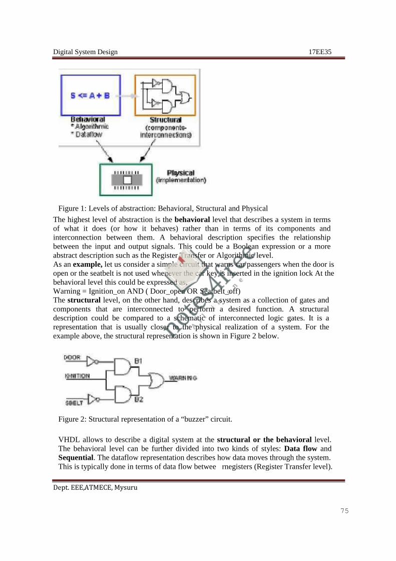
Figure 1: Levels of abstraction: Behavioral, Structural and Physical
The highest level of abstraction is the behavioral level that describes a system in terms of what it does (or how it behaves) rather than in terms of its components and interconnection between them. A behavioral description specifies the relationship between the input and output signals. This could be a Boolean expression or a more abstract description such as the Register Transfer or Algorithmic level. As an example, let us consider a simple circuit that warns car passengers when the door is open or the seatbelt is not used whenever the car key is inserted in the ignition lock At the behavioral level this could be expressed as, Warning = Ignition_on AND ( Door_open OR Seatbelt_off) The structural level, on the other hand, describes a system as a collection of gates and components that are interconnected to perform a desired function. A structural description could be compared to a schematic of interconnected logic gates. It is a representation that is usually closer to the physical realization of a system. For the example above, the structural representation is shown in Figure 2 below.
Figure 2: Structural representation of a “buzzer” circuit.
VHDL allows to describe a digital system at the structural or the behavioral level. The behavioral level can be further divided into two kinds of styles: Data flow and Sequential. The dataflow representation describes how data moves through the system. This is typically done in terms of data flow betwee rnegisters (Register Transfer level).
75

Digital System Design 17EE35
Dept. EEE,ATMECE, Mysuru
The data flow model makes use of concurrent statements that are executed in parallel as soon as data arrives at the input. On the other hand, sequential statements are executed in the sequence that they are specified. VHDL allows both concurrent and sequential signal assignments that will determine the manner in which they are executed. Mixed level design consists both behavioral and structural design in one block diagram.
5.4 Basic Structure of a VHDL file
(a) Entity A digital system in VHDL consistosf a design entity that can contain other entities that
are then considered components of the top-level entity. Each entity is modeled by an entity declaration and an architecture body. One can consider the entity declaration as the interface to the outside world that defines the input and output signals, while the architecture body contains the description of the entity and is composed of interconnected entities, processes and components, all operating concurrently, as schematically shown in Figure 3 below. In a typical design there will be many such entities connected together to perform the desired function. A VHDL entity consisting of an interface (entity declaration) and a body (architectural description).
a. Entity Declaration The entity declaration defines the NAME of the entity and lists the input and output ports. The general form is as follows, entity NAME_OF_ENTI
TY is [ generic generic_declarations);]
port (signal_names: mode
type;
signal_names: : signal_names:
mode
mode
type; type);
end [NAME_OF_ENTITY] ;
An entity always starts with the keyword entity, followed by its name and the keyword is. Next are the port declarations using the keyword port . An entity declaration always ends with the keyword end, optionally [] followed by the name of the entity.
76

Digital System Design 17EE35
Dept. EEE,ATMECE, Mysuru
Figure 3: Block diagram of Full Adder Example entity
1: FULLADDER is
-- (After a double minus sign (-) the rest of -- the --
line is treated as a comment)
-- Interface description of FULLADDER port ( x, y, Ci: in bit; S, CO:
out bit);
end FULLADDER; The module FULLADDER has five interface ports. Three of them are the input ports x, y and Ci indicated by the VHDL keyword in. The remaining two are the output ports S and CO indicated by out. The signals going through these ports are chosen to be of the type bit . The type bit consists of the two characters '0' and '1' and represents the binary logic values of the signals. ∉ The NAME_OF_ENTITY is a user-selected identifier
signal_names consists of a comma separated list of one or more user-selected identifiers that specify external interface signals.
∉ mode: is one of the reserved words to indicate the signal direction:
o in – indicates that the signal is an input o out – indicates that the signal is an output of the entity whose value can only be read by other entities that use it. o buffer – indicates that the signal is an output of the entity whose value can be read inside the entity’s architecture o inout – the signal can be an input or an output. ∉ type: a built-in or user-defined signal type. Examples of types are bit, bit_vector, Boolean, character, std_logic, and stc_ulogic. o bit – can have the value 0 and 1 o bit_vector – is a vector of bit values (e.g. bit_vector (0 to 7) o std_logic, std_ulogic, std_logic_vector, std_ulogic_vector: can have 9 values to indicate the value and strength of a signal. Std_ulogic and
77

Digital System Design 17EE35
Dept. EEE,ATMECE, Mysuru
std_logic are preferred over the bit or bit_vector types. o boolean – can have the value TRUE and FALSE o integer – can have a range of integer values o real – canhave a range of real values o character – any printing character o time – to indicate time ∉ generic: generic declarations are optional Example 2:
Example 3:
entity mux4_to_1 is port (I0,I1,I2,I3: in std_logic;
78

Digital System Design 17EE35
Dept. EEE,ATMECE, Mysuru
S: in std_logic_vector(1downto 0);
79

Digital System Design 17EE35
Dept. EEE,ATMECE, Mysuru
y: out std_logic); end mux4_to_1; Example 4: D Flip-Flop:
entity dff_sr is
port (D,CLK,S,R: in std_logic; Q,Qb: out std_logic); end dff_sr; Architecture body The architecture body specifies how the circuit operates and how it is implemented. As discussed earlier, an entity or circuit can be specified in a variety of ways, such as behavioral, structural (interconnected components), or a combination of the above. The architecture body looks as follows, architecture architecture_name of NAME_OF_ENTITY is -- Declarations -- components declarations -- signal declarations -- constant -- function
declarations declarations
-- procedure declarations -- type :
declarations
begin -- Statements : end architecture_name; The types of Architecture are: (a) The behavioral Model (b) Structure Model (c) Mixed Model (a) Behavioral model The architecture body for the example of Figure 2, described at the behavioral level, is given below,
80

Digital System Design 17EE35
Dept. EEE,ATMECE, Mysuru
Example 1: architecture begin
behavioral of BUZZER is
WARNING <=
(not DOOR
and IGNITION) or (not SBELT
and
IGNITION); end behavioral; The header line of the architecture body defines the architecture name, e.g. behavioral, and associates it with the entity, BUZZER. The architecture name can be any legal identifier. The main body of the architecture starts with the keyword begin and gives the Boolean expression of the function. We will see later that a b haevioral model can be described in several other ways. The “<=” symbol represents an assignment operator and assigns the value of the expression on the right to the signal on the left. The architecture body ends with an end Example 2:
keyword followed by the architecture name.
The behavioral description of a 3 input AND gate is shown below. entity AND3 is port (in1, in2, in3: in std_logic; out1: out std_logic); end AND3; architecture
behavioral_2 of AND3is
81

Digital System Design 17EE35
Dept. EEE,ATMECE, Mysuru
begin out1 <= in1 and in2 and in3; end behavioral_2; Example 3: entity XNOR2 is port (A, B: in std_logic; Z: out std_logic); end XNOR2; architecture behavioral_xnor of XNOR2 is -- signal declaration (of internal signals X, Y) signal X, Y: begin
std_logic;
X <= A and B; Y <
= (not A) and (not B);
Z <= X or Y; End behavioral_xnor; Example 4: SR Flip Flop: entity SRFF is port (S, R: in std_logic; Q, Qb: out std_logic); end SRFF; architecture begin
behavioral_2 of SRFF is
Q <=
NOT
(S and Qb);
Qb <= NOT ( R and Q); end behavioral_2; The statements in the body of the architecture make use of logic operators. In addition, other types of operators including relational, shift, arithmetic are allowed as well. Concurrency The signal assignments in the above examples are concurrent statements. This implies that the statements are executed when one or more of the signals on the right hand side change their value (i.e. an event occurs on one of the signals). In general, a change of the current value of a signal is called an event. For instance, when the input S (in SR FF) changes, the first expression gets evaluated, which changes the value of Q, change in Q in turn triggers second expression and evaluates Qb. Thus Q and Qb are updated concurrently. There may be a propagation delay associated with this change. Digital systems are basically data-driven and an event which occurs on one signal will lead to an event on another signal, etc. Hence, the execution of the statements is determined by the flow of signal values. As a result, the order in which these statements are given does not matter (i.e., moving the statement for the output Z ahead of that for X and Y does not change the outcome). This is in contrast to conventional, software programs that execute the statements in a sequential or procedural manner. Example 5
82
Digital System Design 17EE35
Dept. EEE,ATMECE, Mysuru
architecture begin
CONCURRENT
of FULLADDER is
S <=
x xor y xor Ci after 5 ns;
CO <=
(x and y)
or (y and Ci) or (x and Ci) after 3 ns;
83

Digital System Design 17EE35
Dept. EEE,ATMECE, Mysuru
Example2: architecture CONCURRENT_VERS
ION2 of FULLADDER is
signal begin
PROD1,
PROD2,
PROD3
: bit;
SUM <=
A xor B xor C; -- statement 1
CARRY
<= PROD1
or PROD2 or PROD3;
-- statement 2
PROD1 PROD2 PROD3
<= A <= B <= A
and and and
B; -- C; -- C; --
statement 3 statement 4 statement 5
end CONCURRENT_VERSION2; (a) Concurrent statement: In VHDL With select and When else statements are called as concurrent statements and they do not require Process statement Example 1: VHD
L code for 4:1 multiplexor
library ieee; use ieee.std_logic_1164.all; entity Mux is port ( I: in std_logic_vector(3 downto 0); S: in std_logic_vector(1 downto 0); y: out std_logic); end Mux; -- architecture using logic expression architecture begin
behv1 of Mux is
y<= (not(s(0)) and not(s(1)) and I(0)) or(s(0) and not(s(1)) and I(1)) or (not(s(0)) and s(1) and I(2))or (s(0) and s(1) and I(3)); end behv1; -- Architecture using when..else: architecture begin
behv2 of Mux is
y <= I(0) when S="00" else I(1) I(2) I(3)
when when when
S="01" S="10" S="11"
else else else
‘Z’ ;
84

Digital System Design 17EE35
Dept. EEE,ATMECE, Mysuru
end behv2; -- architecture using with select statement architecture begin
behv3 of Mux is
with s select y<=i(0) when “00”, i(1) i(2) i(3)
when when when
“01”, “10”, “11”,
‘Z’ when others; end behv3; Note: ‘Z’ high impedence state should be entered in capital Z Example 2: SR flipflop using when else statement entity SRFF is port ( S, R: in bit; Q, QB: inout bit); end RSFF; architecture begin
beh of RSFF is
Q <= Q when S= ‘0’ and R = ‘0’ else ‘0’ ‘1’
when S when S
= ‘0’ = ‘1’
and R and R
= ‘1’ = ’0’
else else
‘Z’; QB <= not(Q); end beh; The statement WHEN…..ELSE conditions are executed one at a time in sequential order until the conditions of a statement are met. The first statement that matches the conditions required assigns the value to the target signal. The target signal for this example is the local signal Q. Depending on the values of signals S and R, the values Q,1,0 and Z are assigned to Q. If more than one statements conditions match, the first statement that matches does the assign, and the other matching state. In with …select statement all the alternatives arte checked simultaneously to find a matching pattern. Therefore the with … select must cover all possible values of the selector Structural Descriptions A description style where different components of an architecture and their interconnections are specified is known as a VHDL structural description. Initially, these components are declared and then components' instances are generated or instantiated. At the same time, signals are mapped to the components' ports in order to connect them like wires in hardware. VHDL simulator handles component instantiations as concurrent assignments. Syntax: component declaration:
85

Digital System Design 17EE35
Dept. EEE,ATMECE, Mysuru
component [generic
component_name (generic_list:
type_name
[:=
expression] {;
generic_list: type_name [:= expression]} );] [port (signal_list: in|out|inout|buffer type_name {; signal_list: in|out|inout|buffer type_name} );] end component;
Component instantiation: component_label: component_name port ma
p (signal_mapping);
The mapping of ports to the connecting signals during the instantiation can be done through the positional notation. Alternatively, it may be done by using the named notation. If one of the ports has no signal connected to it (this happens, for example, when there are unused outputs), a reserved word open may be used. Example 1: signal_mapping: declaration_name => signal_name. entity RSFF is port ( SET, RESET: in bit; Q, end
QBAR: RSFF;
inout bit);
architecture NETLIST
of RSFF is
component NAND2 port (A, B: in bit; C: out bit); end component; begin U1: NAN
D2 port ma
p (SET, QBA
R, Q);
U2: NAND2
port map
(Q, RESET,
QBAR);
end NETLIST; --- named notation instantiation: --- U1: NAN
D2 port map (A => SET, C => Q, B => QBAR);
Figure 1: Schematic of SR FF using NAND Gate
The lines between the first and the keyword begin are a component declaration. It
86

Digital System Design 17EE35
Dept. EEE,ATMECE, Mysuru
describes the interface of the entity nand_gate that we would like to use as a component in (or part of) this design. Between the begin and end keywords, the statements define component instances. There is an important distinction between an entity, a component, and a component instance in VHDL. The entity describes a design interface, the component describes the interface of an entity that will be used as an instance (or a sub-block), and the component instance is a distinct copy of the component that has been connected to other parts and signals. In this example the component nand_gate has two inputs (A and B) and an output ©. There are two instances of the nand_gate compone nt in this architectureoc rresponding to the two nand symbols in the schematic. The first instance refers to the top nand gate in
the schematic and the statement is called the component instantiation statement. The first word of the component instantiation statement (u1:nand2) gives instance a name, u1, and specifies that it is an instance of the component nand_gate. The next words describes how the component is connected to the set of the design using the port map clause. The port map clause specifies what signals of the design should be connected to the interface of the component in the same order as they are listed in the component declaration. The interface is specified in order as A, B and then C, so this instance connects set to A, QBAR to B and Q to C. This corresponds to the way the top gate in the schematic is connected. The second instance, named n2, connects RESET to A, Q to A, and QBAR to C of a different instance of the same nand_gate component in the same manner as shown in the schematic.
The structural description of a design is simply a textual description of a schematic. A list of components and there connections in any language is also called a netlist. The structural description of a design in VHDL is one of many means of specifying netlists
87

Digital System Design 17EE35
Dept. EEE,ATMECE, Mysuru
.
Example 2: Four
Bit Adder – Illustrating a structural VHDL
model:
Figure 2: 4-bit Adder using four Full Adders. -- Example of a four bit adder library ieee; use ieee.std_logic_1164.all; -- definition of a full adder entity FULLADDER is port (x, y, ci: in std_logic; s, co: out std_logic); end FULLADDER; architecture begin
fulladder_behav of FULLADDER is
s <= x xor y xor ci ; co <= (x and y) or (x and ci)or(y and ci)); end fulladder_behav;
88

Digital System Design 17EE35
Dept. EEE,ATMECE, Mysuru
-- 4-bit adder library ieee; use ieee.std_logic_1164.all; entity FOURBITADD is port (a, b: in std_logic_vector(3 downto 0); Cin : in std_logic; sum: out std_logic_vector (3 downto 0); Cout: out std_logic); end FOURBITADD; architecture fouradder_structure of FOURBITADD is signal c: std_logic_vector (4 downto 0); component FULLADDER port (x, y, ci: in std_logic; s, co: out std_logic); end component; begin FA0: FULLADDER port ma
p (a(0), b(0), Cin, sum(0), c(1));
FA1: FULLADDER port ma
p (a(1), b(1), C(1), sum(1), c(2));
FA2: FULLADDER port ma
p (a(2), b(2), C(2), sum(2), c(3));
FA3: FULLADDER port ma
p (a(3), b(3), C(3), sum(3), c(4));
Cout <= c(4); end fouradder_structure; We needed to define the internal signals c (4 downto 0) to indicate the nets that connect the output carry to the input carry of the next full adder. For the first input we used the input signal Cin. For the last carry we defined c (4) as an internal signal. We could not use the output signal Cout since VHDL does not allow the use of outputs as internal signals! For this reason we had to define the internal carry c(4) and assign c(4) to the output carry signal Cout.
5.5 Operators
(a) VHDL Operators VHDL supports different classes of operators that operate on signals, variables and constants. The different c lasses ofpeorators are summarized below.
89

Digital System Design 17EE35
Dept. EEE,ATMECE, Mysuru
The order of precedence is the highest for the operators of class 7, followed by class 6 with the lowest prec dence for class 1. Unless parentheses are used, the operators with the highest precedence are applied first. Operators of the same class have the same precedence and are applied from left to right in an expression. As an example, consider the following std_ulogic_vectors, X (=’010’), Y(=’10’), and Z (‘10101’). The expression not X & Y xor Z rol 1 is equivalent to ((not X) & Y) xor (Z rol 1) = ((101) & 10) xor (01011) =(10110) xor (01011) = 11101. The xor is executed on a bit-per-bit basis. 1. Logic operators The logic operators (and, or, nand, nor, xor and xnor) are defined for the “bit”, “boolean”, “std_logic” and “std_ulogic” types and their vectors. They are used to define Boolean logic expression or to perform bit-per-bit operations on arrays of bits. They give a result of the same type as the operand (Bit or Boolean). These operators can be applied to signals, variables and constants. Notice that the nand and nor operators are not associative. One should use parentheses in a sequence of nand or nor operators to prevent a syntax error: X nand Y nand Z will give a syntax error and should be written as (X nand Y) nand Z. 2. Relational operators The relational operators test the relative values of two scalar types and give as result a Boolean output of “TRUE” or “FALSE”.
90

Digital System Design 17EE35
Dept. EEE,ATMECE, Mysuru
Notice that symbol of the operator “<=” (smaller or equal to) is the same one as the assignment operator used to assign a value to a signal or variable. In the following examples the first “<=” symbol is the assignment operator. Some examples of relational operations are: variable STS : Boolean; constant A : integer :=24; constant B_COUNT : integer :=32; constant C : integer :=14; STS <= (A < B_COUNT) ; -- will assign the value “TRUE” to STS STS <= ((A >= B_COUNT) or (A > C)); -- will result in “TRUE” STS <= (std_logic (‘1’, ‘0’, ‘1’) < std_logic(‘0’, ‘1’,’1’));--makes STS “FALSE” type new_std_logic is (‘0’, ‘1’, ‘Z’, ‘-‘);
variable A1: new_std_logic :=’1’; variable A2: new_std_logic :=’Z’; STS <= (A1 < A2); will result in “TRUE” since ‘1’ occurs to the left of ‘Z’. For discrete array types, the comparison is done on an element-per-element basis, starting from the left towards the right, as illustrated by the last two examples. 3. Shift operators
Thesepeorators perform a bit-wise shift or rotate operation on a one-dimensional array of elements of the type bit (or std_logic) or Boolean.
91

Digital System Design 17EE35
Dept. EEE,ATMECE, Mysuru
The operand is on the left of the operator side of the operator. As an example,
andhet number (integer) of shifts is on the right
variable NUM1 :bit_vector := “10010110”; NUM1 srl 2; will result in the number “00100101”. When a negative integer is given, the opposite action occurs, i.e. a shift to the left will be a shift to the right. As an example NUM1 srl –2 would be equivalent to NUM1 sll 2 and give the result “01011000”. Other examples of shift operations are for the bit_vector A = “101001” variable A: bit_vector :=”101001”;
92

Digital System Design 17EE35
Dept. EEE,ATMECE, Mysuru
4. Addition operators
The addition operators are used to perform arithmetic operation (addition and subtraction) on operands of any numeric type. The concatenation (&) operator is used to concatenate two vectors together to make a longer one. In order to use these operators one has to specify the ieee.std_logic_unsigned.all or std_logic_arith package package in addition to the ieee.std_logic_1164 package.
An example of concatenation is the grouping of signals into a single bus [4]. signal MYBUS :std_log ic_vectro (15 downto 0); signal STATUS :std_logic_vector (2 downto 0); signal RW, CS1, CS2 :std_logic; signal MDATA :std_logic_vector ( 0 to 9); MYBUS <= STATUS & RW & CS1 & CS2 & MDATA; Other examples are MYARRAY (15 downto 0) <= “1111_1111” & MDATA (2 to 9); NEWWORD <= “VHDL” & “93”; The first example results in filling up the first 8 leftmost bits of MYARRAY with 1’s and the rest with the 8 rightmost bits of MDATA. The last example results in an array of characters “VHDL93”. Example:
93

Digital System Design 17EE35
Dept. EEE,ATMECE, Mysuru
Signal a: std_logic_vector (3 downto 0); Signal b: std_logic_vector (3 downto 0); Signal y:std_logic_vector (7 downto 0); Y<=a & b;
5. Unary operators The unary operators “+” and “-“ are used to specify the sign of a numeric type.
6. Multiplying operators The multiplying operators are used to perform mathematical functions on numeric types (integer or floating point).
The multiplication operator is also defined when one of the operands is a physical type and the other an integer or real type. The remainder (rem) and modulus (mod) are defined as follows: A rem B = A –(A/B)*B (in which A/B in an integer)
94

Digital System Design 17EE35
Dept. EEE,ATMECE, Mysuru
A mod B = A – B * N (in which N is an integer) The result of the rem operator has the sign of its first operand while the result of the mod
operators has the sign of the second operand. Some examples of these operators are given below. 11 rem 4 results in 3 (-11) rem 4 results in -3 9 mod 4 results in 1 7 mod (-4) results in –1 (7 – 4*2 = -1). 7. Miscellaneous operators These are the absolute value and exponentation operators that can be applied to numeric types. The logical negation (not) results in the inverse polarity but the same type.
VHDL data types: To define new type user must create a type declaration. A type declaration defines the name of the type and the range of the type. Type declarations are allowed in (i) Package declaration (ii) Entity Declaration (iii) Architecture Declaration (iv)Subprogram Declaration (v) Process Declaration
95
Digital System Design 17EE35
Dept. EEE,ATMECE, Mysuru
Enumerated Types: An Enumerated type is a very powerful tool for abstract modeling. All of the values of an enumerated type are user defined. These values can be identifiers or single character literals. An identifier is like a name, for examples: day, black, x Character literals are single characters enclosed in quotes, for example: ‘x’, ‘I’, ‘o’ Type Fourval is (‘x’, ‘o’, ‘I’, ‘z’); Type color is (red, yello, blue, green, orange); Type Instruction is
s(add, sub, lda, ldb, sta, stb, outa, xfr);
96

Digital System Design 17EE35
Dept. EEE,ATMECE, Mysuru
Real type example: Type
input level is range -10.0 to +10.0
Type
probability is range 0.0 to 1.0;
Type
W_Day
is (MON, TUE,
WED,
THU,
FRI, SAT,
SUN);
type dollars is range 0 to 10;
variable day: W_Day; variable Pkt_money:Dollars; Case When
Day is TUE =>
pkt_money:=6;
When
MON
OR WED=>
Pkt_money:=2;
When End
others case;
=> Pkt_money:=7;
Example for enumerated type - Simple Microprocessor model: Package instr is Type End
instruction is instr;
(add, sub, lda, ldb, sta, stb, outa, xfr);
Use work.instr.all; Entity mp is PORT
(instr: in Instruction;
Addr: in Integer; Data: inout integer); End mp; Architecture mp Begin
of mp is
Process (instr) type reg is array(0 to 255) of integer; variable variable begin
a,b: reg:
integer; reg;
case instr is when when when when when
lda => ldb => add => sub => sta =>
a:=data; b:=data; a:=a+b; a:=a-b; reg(addr)
:= a;
97

Digital System Design 17EE35
Dept. EEE,ATMECE, Mysuru
when
stb => reg(addr):= b;
when when end
outa => xfr =>
case;
data a:=b;
:= a;
end end
process; mp;
Physical types: These are used to represent real world physical qualities such as length, mass, time and current. Type is range to Units identifier; {(identifier=physical literal;)} end units identifier; Examples: (1) Type
resistance is range 0 to 1E9
units ohms; kohms =
1000ohms;
98

Digital System Design 17EE35
Dept. EEE,ATMECE, Mysuru
Mohms = 1000kohms; end units; (2) Type units na;
current is range 0 to 1E9
ua = ma = a =
1000na; 1000ua;
1000ma; end units;
Composite Types: Composite types consist of array and record types. ∉ Array types are groups of elements of same type ∉ Record allow the grouping of elements of different types ∉ Arrays are used for modeling linear structures such as ROM, RAM ∉ Records are useful for modeling data packets, instruction etc. ∉ A composite type can have a value belonging to either a scalar type, composite type or an access type. Array Type: Array type groupasre one or more elements of the same type together as a single object. Each element of the array can be accessed by one or more array indices. Type
data-bus is array (0to 31) of BIT;
Variable x: Variable y:
data-bus; bit;
Y := Y :=
x(0); x(15);
Type
address_word is array (0 to 63) of BIT;
Type
data_word is array (7 downto 0) of std_logic;
Type
ROM is
array (0 to 255) of data_word;
We can declare array objects of type mentioned above as follows: Variable ROM_data: ROM; Signal Address_bus: Address_word; Signal word: data_word; Elements of an array can be accessed by specifying the index values into the array. X<= Address_bus(25); transfers 26th element of array Address_bus to X. Y := ROM_data(10)(5); transfers the value of 5th element in 10th row. Multi dimentional array types may also be defined with two or more dimensions. The following example defines a two-dimensional array variable, which is a matrix of integers with four rows and three columns: Type matrix4x3 is array (1 to 4, 1 to 3) of integer; Variable matrixA: matrix4x3 := ((1,2,3), (4,5,6), (7,8,9), (10,11,12)); Variable m:integer; The viable matrixA, will be initialized to 1 2 3
99

Digital System Design 17EE35
Dept. EEE,ATMECE, Mysuru
4 5 6 7 8 9 10 11 12 The array element matrixA(3,2) references the element in the third row and second column, which has a value of 8. m := matrixA(3,2); m gets the value 8
Record Type: Record Types group objects of many types together as a single object. Each element of the record can be accessed by its field name. Record elements can include elements of any type including arrays and records. Elements of a record can be of the same type or different types. Example: Type
optype is (add, sub, mpy, div, cmp);
Type instruction is Record Opcode :
optype;
Src Dst
: integer; : integer;
End record;
Structure of Verilog module:
module module_name(signal_names) Signal_type signal_names; Signal_type signal_names; Aasign statements Assign statements Endmodule_name
Verilog Ports: � Input: The port is only an input port.I. In any assignment statement, the port
should appear only on the right hand side of the statement � Output: The port is an output port. The port can appear on either side of the
assignment statement. � Inout: The port can be used as both an input & output. The inout represents a
bidirectional bus. Verilog Value Set:
� 0 represents low logic level or false condition
� 1 represents high logic level or true condition
� x represents unknown logic level
100

Digital System Design 17EE35
Dept. EEE,ATMECE, Mysuru
� z represents high impedance logic level
Verilog Operators Operators in Verilog are the same as operators in programming languages. They take two values and compare or operate on them to yield a new result. Nearly all the operators in Verilog are exactly the same as the ones in the C programming language.
Operator Type Operator
Symbol
Operation
Performed
Arithmetic * Multiply
/ Division
+ Addition
- Subtraction
% Modulus
+ Unary plus
i Unary minus
Relational > Greater than
< Less Than
>=
Greater than or equal to
<= Less than or equal to
Equality == Equality
!= Inequality
Logical ! Logical Negation
&& Logical And
|| Logical Or
Shift >> Right Shift
<< Left Shift
Conditional ? Conditional
Reduction ~ Bitwise negation
101

Digital System Design 17EE35
Dept. EEE,ATMECE, Mysuru
~& Bitwise nand
| Bitwise or
~| Bitwise nor
^ Bitwise xor
^~ Bitwise xnor
~^ Bitwise xnor
Concatenation {}
102

Digital System Design 17EE35
Dept. EEE,ATMECE, Mysuru
103

Digital System Design 17EE35
Dept. EEE,ATMECE, Mysuru
Examples: x = y + z; //x will get the value of y added to the value of z x = 1 >> 6; //x will get the value of 1 shifted right by 5 positions x = !y //x will get the value of y inverted. If y is 1, x is 0 and vise versa
Verilog Data Types: Nets (i) an be thought as hardware wires driven by logic Equal z when unconnected Various types of nets wire wand wor tri
(wired-AND) (wired-OR) (tri-state)
In following examples: Y is evaluated, automatically, every time A or B changes
Nets (ii)
A
B Y
wire Y; // declaration assign Y = A & B;
wand Y; // declaration
assign Y = A; assign Y = B;
A
YB
104

Digital System Design 17EE35
Dept. EEE,ATMECE, Mysuru
wor Y; // declaration
assign Y = A; assign Y = B;
dr
A Y
tri Y;
// declaration
Registers:
assign Y = (dr) ? A : z;
� Variables that store values � Do not represent real hardware but .. � .. real hardware can be implemented with registers � Only one type: reg
reg A, C; // declaration // assig A = 1;
nmentasre always done inside a procedure
C = A; // C gets the logical value 1 A = 0; // C is still 1 C = 0; // C is now 0
� Register values are updated explicitly!! Vectors: � Represent buses
wire [3:0] busA; reg [1:4] busB; reg [1:0] busC;
� Left number is MS bit � Slice management
� Vector assignment (by position!!)
busC[1] = busA[2]; busC[0] = busA[1];
Integer & Real Data Types:
busB[1] = busA[3]; busB[2] = busA[2]; busB[3] = busA[1]; busB[4] = busA[0];
� Declaration integer i, k; real r;
Use as registers (inside procedures)
105

Digital System Design 17EE35
Dept. EEE,ATMECE, Mysuru
i = 1; // assignments occur inside procedure r = 2.9; k = r; // k is rounded to 3
� Integers are not initialized!! � Reals are initialized to 0.0
Parameters: � Parameters represents global constants.They are declared by the predefined word
parameter. module comp_genr(X,Y,XgtY,XltY,XeqY); parameter N = 3; input [ N :0] X,Y; output XgtY,XltY,XeqY; wire [N:0] sum,Yb;
Time Data Type:
� Special data type for simulation time measuring � Declaration
time my_time; � Use inside procedure
my_time = $time; // get current sim time � Simulation runs at simulation time, not real time Arrays (i):
Syntax integer count[1:5]; // 5 integers reg var[-15:16]; // 32 1-bit regs reg [7:0] mem[0:1023]; // 1024 8-bit regs
Accessing array elements Entire element: mem[10] = 8’b 10101010; Element subfield (needs temp storage): reg [7:0] temp; .. temp = mem[10]; var[6] = temp[2]; Strings: Implemented with regs:
reg [8*13:1] string_val; // can hold up to 13 chars .. string_val = “Hello Verilog”; string_val = “hello”; // MS Bytes are filled with 0 string_val = “I am overflowed”; // “I ” is truncated
Escaped chars: \n newline \t tab
106

Digital System Design 17EE35
Dept. EEE,ATMECE, Mysuru
%% % \\ \ \“ “ Styles(Types) of Descriptions:
� Behavioral Descriptions � Structural Descriptions � Switch – Level Descriptions � Data – Flow Descriptions � Mixed Type Descriptions Behavioral Descriptions: VHDL Behavioral description entity half_add is
port (I1, I2 : in bit; O1, O2 : out bit); end half_add; architecture behave_ex of half_add is
--The architecture consists of a process construct begin
process (I1, I2) --The above statement is process statement
O1 <= I1 xor I2 after 10 ns; O2 <= I1 and I2 after 10 ns;
end process; end behave_ex; Verilog behavioral Description: module half_add (I1, I2, O1, O2);
input I1, I2; output O1, O2; reg O1, O2; always @(I1, I2) //The above abatement is always //The module consists of always construct begin
#10 O1 = I1 ^ I2; #10 O2 = I1& I2;
end endmodule
VHDL Structural Descriptions: entity system is
port (a, b : in bit; sum, cout : out bit);
end system; architecture struct_exple of system is component xor2 --The above statement is a component statement
port(I1, I2 : in bit; O1 : out bit);
begin
107

Digital System Design 17EE35
Dept. EEE,ATMECE, Mysuru
end component; component and2
port(I1, I2 : in bit; O1 : out bit);
end component; begin
X1 : xor2 port map (a, b, sum); A1 : and2 port map (a, b, cout);
end struct_exple; Verilog Structural Description: module system(a, b, sum, cout);
input a, b; output sum, cout;
xor X1(sum, a, b); //The above statement is EXCLUSIVE-OR gate
and a1(cout, a, b); //The above statement is AND gate endmodule
Switch Level Descriptions: VHDL Description: library IEEE; use IEEE.STD_LOGIC_1164.ALL; entity Inverter is
Port (y : out std_logic; a: in std_logic ); end Inverter; architecture Invert_switch of Inverter is component nmos --nmos is one of the key words for switch-level. port (O1: out std_logic; I1, I2 : in std_logic); end component; component pmos --pmos is one of the key words for switch-level. port (O1: out std_logic ;I1, I2 : in std_logic); end component; for all: pmos use entity work. mos (pmos_behavioral); for all: nmos use entity work. mos (nmos_behavioral); --The above two statements are referring to a package mos --See details in Chapter 5 constant vdd: std_logic := '1'; constant gnd : std_logic:= '0'; begin p1 : pmos port map (y, vdd, a); n1: nmos port map (y, gnd, a); end Invert_switch;
108

Digital System Design 17EE35
Dept. EEE,ATMECE, Mysuru
Verilog switch – Level Description: module invert(y,a); input a; output y; supply1 vdd; supply0 gnd; pmos p1(y, vdd, a); nmos n1(y, gnd, a); --The above two statement are using the two primitives pmos and nmos endmodule Data – Flow Descriptions: VHDL Data – Flow Description: entity halfadder is port (a,b: in bit;
s,c: out bit); end halfadder; architecture HA_DtFl of halfadder is
begin s <= a xor b; c <= a and b;
end HA_DtFl; Verilog Data – Flow Description: module halfadder (a,b,s,c);
input a; input b; output s; output c;
assign s = a ^ b; assign c = a & b;
endmodule 5.6 Comparision of VHDL & Verilog: � Data Types VHDL: Types are in built in or the user can create and define them.User defined types give the user a tool to write the code effectively. VHDL supports multidimensional array and physical type. Verilog: Verilog data types are simple & easy to use. There are no user defined types. � Ease of Learning VHDL:Hard to learn because of its rigid type requirements. Verilog: Easy to learn,Verilog users just write the module without worrying about what Library or package should be attached. � Libraries and Packages VHDL:Libraries and packages can be attached to the standard VHDL package.Packages can include procedures and functions, & the package can be made available to any module that needs to use it.
109

Digital System Design 17EE35
Dept. EEE,ATMECE, Mysuru
Verilog:No concept of Libraries or packages in verilog.
� Operators VHDL:An extensive set of operators is available in VHDL,but it does not have predefined unary operators. Verilog: An extensive set of operators is also available in verilog. It also has predefined unary operators. � Procedures and Tasks VHDL:Concurrent procedure calls are allowed. This allows a function to be written inside the procedure’s body.This feature may contribute to an easier way to describe a complex system. Verilog:Concurrent task calls are allowed.Functions are not allowed to be written in the task’s body.
ASSIGNMENT QUESTIONS 1) Explain entity and architecture with an example 2) Explain structure of verilog module with an example 3) Explain VHDL operators in detail. 4) Explain verilog operators in detail. 5) Explain how data types are classified in HDL. Mention the advantages of VHDL data types over verilog. 6) Mention the types of HDL descriptions. Explain dataflow and behavioral descriptions
7) Describe different types of HDL description with suitable example. 8) Mention different styles (types) of descriptions. Explain mixed type and mixed
language descriptions. 9) Compare VHDL and Verilog 10) Write the result of all shift and rotate operations inVHDL after applying them to a 7
bit vector A = 1001010 11) Explain composite and access data types with an example for each. 12) Discuss different logical operators used in HDL’s
110

Digital System Design 17EE35
Dept. EEE,ATMECE, Mysuru
5.7 DATA FLOW DESCRIPTIONS
Data flow is one type(style) of hardware description. Facts
∉ Data – flow descriptions simulate the system by showing how the signal flows from system inputs to outputs.
∉ Signal – assignment statements are con ucrrent. At any simulation time, all signal- assignment statements that have an event are executed concurrently.
5.8 VHDL Description and structure entity system is
port (I1, I2 : in bit; O1, O2 : out bit); end; architecture dtfl_ex of system is begin
O1 <= I1 and I2; -- statement 1. O2 <= I1 xor I2; -- statement 2.
--Statements 1 and 2 are signal-assignment statements
end dtfl_ex;
Verilog Description module system (I1, I2, O1, O2);
input I1, I2; output O1, O2;
/*by default all the above inputs and outputs are 1-bit signals.*/
assign O1 = I1&I2; // statement 1 assign O2 = I1^I2; // statement 2
/*Statements 1 and 2 are continuous signal-assignment statements*/ endmodule
Signal Declaration and Assignment Statements: Syntax: signal list_of_signal_names: type [ := initial value]; Examples: signal SUM, CARRY: std_logic; signal DATA_BUS: bit_vector (0 to 7); signal VALUE: integer range 0 to 100;
� Signals are updated after a delta delay. Example: SUM <= (A xor B);
� The result of A xor B is transferred to SUM after a delay called simulation Delta which is a infinitesimal small amount of time.
Constant: Syntax:
111

Digital System Design 17EE35
Dept. EEE,ATMECE, Mysuru
constant list_of_name_of_constant: type [:=initial value] ;
Examples: constant constant
RISE_FALL_TME: time := 2 ns; DELAY1: time := 4 ns;
HDL Code for Half Adder—VHDL and Verilog:
VHDL Half Adder Description
entity halfadder is port ( a : in bit; b : in bit; s : out bit; c : out bit); end halfadder; architecture HA_DtFl of halfadder is begin
s <= a xor b; -- This is a signal assignment statement. c <= a and b; -- This is a signal assignment statement.
end HA_DtFl;
Verilog Half Adder Description module halfadder (a, b, s, c); input a; input b; output s; output c; /*The default type of all inputs and outputs is a single bit. */
assign s = a ^ b; /* This is a signal assignment statement; ^is a bitwise xor logical operator. */
assign c = a & b; /* This is a signal assignment statement & ias bitwise logical “and” operator */
endmodule
112

Digital System Design 17EE35
Dept. EEE,ATMECE, Mysuru
5.8 Data type-vectors
HDL Code of a 2x1 Multiplexer—VHDL and Verilog:
VHDL 2x1 Multiplexer Description :
Fig: 2x1 Multiplexer (a) Logic diagram (b) Logic symbol
library IEEE; use IEEE.STD_LOGIC_1164.ALL; entity mux2x1 is port (A, B, SEL, Gbar : in std_logic;
Y : out std_logic); end mux2x1;
architecture MUX_DF of mux2x1 is signal S1, S2, S3, S4, S5 : std_logic;
Begin
-- Assume 7 nanoseconds propagation delay -- for all and, or, and not.
st1: Y <= S4 or S5 after 7 ns; st2: S4 <= A and S2 and S1 after 7 ns; st3: S5 <= B and S3 and S1 after 7 ns; st4: S2 <= not SEL after 7 ns; st5: S3 <= not S2 after 7 ns; st6: S1 <= not Gbar after 7 ns; end MUX_DF;
113

Digital System Design 17EE35
Dept. EEE,ATMECE, Mysuru
Verilog Description: 2x1 Multiplexer module mux2x1 (A, B, SEL, Gbar, Y); input A, B, SEL, Gbar;
114
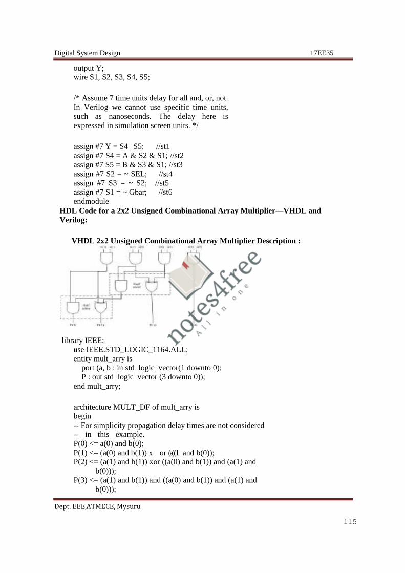
Digital System Design 17EE35
Dept. EEE,ATMECE, Mysuru
output Y; wire S1, S2, S3, S4, S5;
/* Assume 7 time units delay for all and, or, not. In Verilog we cannot use specific time units, such as nanoseconds. The delay here is expressed in simulation screen units. */
assign #7 Y = S4 | S5; //st1 assign #7 S4 = A & S2 & S1; //st2 assign #7 S5 = B & S3 & S1; //st3 assign #7 S2 = ~ SEL; assign #7 S3 = ~ S2; assign #7 S1 = ~ Gbar; endmodule
//st4 //st5 //st6
HDL Code for a 2x2 Unsigned Combinational Array Multiplier—VHDL and Verilog:
VHDL 2x2 Unsigned Combinational Array Multiplier De scription :
library IEEE; use IEEE.STD_LOGIC_1164.ALL; entity mult_arry is
port (a, b : in std_logic_vector(1 downto 0); P : out std_logic_vector (3 downto 0));
end mult_arry;
architecture MULT_DF of mult_arry is begin -- For simplicity propagation delay times are not considered -- in this example. P(0) <= a(0) and b(0); P(1) <= (a(0) and b(1)) x or (a)(1 and b(0)); P(2) <= (a(1) and b(1)) xor ((a(0) and b(1)) and (a(1) and
b(0))); P(3) <= (a(1) and b(1)) and ((a(0) and b(1)) and (a(1) and
b(0)));
115

Digital System Design 17EE35
Dept. EEE,ATMECE, Mysuru
end MULT_DF;
Verilog 2x2 Unsigned Combinational Array Multiplier Description module mult_arry (a, b, P); input [1:0] a, b; output [3:0] P; /*For simplicity, propagation delay times are not considered in this example.*/
assign P[0] = a[0] & b[0]; assign P[1] = (a[0] & b[1]) ^ (a[1] & b[0]); assign P[2] = (a[1] & b[1]) ^ ((a[0] & b[1]) & (a[1] & b[0])); assign P[3] = (a[1] & b[1]) & ((a[0] & b[1])& (a[1] & b[0])); endmodule
HDL Code for a D-Latch—VHDL and Verilog:
VHDL D-Latch Description:
library IEEE; use IEEE.STD_LOGIC_1164.ALL;
entity D_Latch is port (D, E : in std_logic;
Q, Qbar : buffer std_logic); -- Q and Qbar are declared as buffer because they act as --both input and output, they appear on the right and left --hand side of signal assignment statements. inout or -- linkage could have been used instead of buffer. end D_Latch;
architecture DL_DtFl of D_Latch is constant Delay_EorD : Time := 9 ns; constant Delay_inv : Time := 1 ns; begin --Assume 9-ns propagation delay time between --E or D and Qbar; and 1 ns between Qbar and Q.
116

Digital System Design 17EE35
Dept. EEE,ATMECE, Mysuru
Qbar <= (D and E) nor (not E and Q) after Delay_EorD; Q <= not Qbar after Delay_inv;
end DL_DtFl;
Verilog D-Latch Description: module D_latch (D, E, Q, Qbar); input D, E; output Q, Qbar;
/* Verilog treats the ports as internal ports, so Q and Qbar are not considered here as both input and output. If the port is connected externally as bidirectional, then we should use inout. */
time Delay_EorD = 9; time Delay_inv = 1; assign #Delay
(~E & Q)); o_rED Qbar = ~((E & D) |
assign #Delay_inv Q = ~ Qbar; endmodule
HDL Code of a 2x2 Magnitude Comparator—VHDL and Verilog:
VHDL 2x2 Magnitude Comparator Description: library IEEE; use IEEE.STD_LOGIC_1164.ALL;
entity COMPR_2 is port (x, y : in std_logic_vector(1 downto 0); xgty,
xlty : buffer std_logic; xeqy : out std_logic); end COMPR_2;
architecture COMPR_DFL of COMPR_2 is begin xgty <= (x(1) and not y(1)) or (x(0) and not y(1) and
not y(0)) or x(0) and x(1) and not y(0));
xlty <= (y(1) and not x(1)) or ( not x(0) and y(0) and y(1)) or
(not x(0) and not x(1) and y(0)); xeqy <= xgty nor xlty; end COMPR_DFL;
117

Digital System Design 17EE35
Dept. EEE,ATMECE, Mysuru
Verilog 2x2 Magnitude Comparator Description module compr_2 (x, y, xgty, xlty, xeqy); input [1:0] x, y; output xgty, xlty, xeqy; assign xgty = (x[1] & ~ y[1]) | (x[0] & ~ y[1]
& ~ y[0]) | (x[0] & x[1] & ~ y[0]); assign xlty = (y[1] & ~ x[1] ) | (~ x[0] & y[0] & y[1]) |
(~ x[0] & ~ x[1] & y[0]); assign xeqy = ~ (xgty | xlty); endmodule
118

Digital System Design 17EE35
Dept. EEE,ATMECE, Mysuru
3-Bit Ripple-Carry Adder Case Study—VHDL and Verilog
VHDL 3-Bit Ripple-Carry Adder Case Study Description
library IEEE; use IEEE.STD_LOGIC_1164.ALL; entity adders_RL is
port (x, y : in std_logic_vector (2 downto 0); cin : in std_logic; sum : out std_logic_vector (2 downto 0); cout : out std_logic);
end adders_RL;
--I. RIPPLE-CARRY ADDER
architecture RCarry_DtFl of adders_RL is --Assume 4.0-ns propagation delay for all gates. signal c0, c1 : std_logic; constant delay_gt : time := 4 ns;
begin sum(0) <= (x(0) xor y(0)) xor cin after 2*delay_gt;
--Treat the above statement as two 2-input XOR.
sum(1) <= (x(1) xor y(1)) xor c0 after 2*delay_gt;
--Treat the above statement as two 2-input XOR.
119

Digital System Design 17EE35
Dept. EEE,ATMECE, Mysuru
sum(2) <= (x(2) xor y(2)) xor c1 after 2*delay_gt; --Treat the above statement as two 2-input XOR. c0 <= (x(0) and y(0)) or (x(0) and cin) or (y(0) and cin)
after 2*delay_gt; c1 <= (x(1) and y(1)) or (x
after 2*delay_gt; (1) ancd0) or (y(1) and c0)
cout <= (x(2) and y( after 2*delay_gt;
end RCarry_DtFl;
2)) o(rx(2) and c1) or (y(2) and c1)
Verilog 3-Bit Ripple-Carry Adder Case Study Description module adr_rcla (x, y, cin, sum, cout); input [2:0] x, y; input cin; output [2:0] sum; output cout; // I. RIPPLE CARRY ADDER wire c0, c1; time delay_gt = 4; //Assume 4.0-ns propagation delay for all gates.
assign #(2*delay_gt) sum[0] = (x[0] ^ y[0]) ^ cin; //Treat the above statement as two 2-input XOR.
assign #(2*delay_gt) sum[1] = (x[1] ^ y[1]) ^ c0; //Treat the above statement as two 2-input XOR.
assign #(2*delay_gt) sum[2] = (x[2] ^ y[2]) ^ c1; //Treat the above statement as two 2-input XOR.
assign #(2*delay_gt) c0 = (x[0] & y[0]) | (x[0] & cin) | (y[0] & cin);
assign #(2*delay_gt) c1 = (x[1] & y[1]) | (x[1] & c0) | (y[1] & c0);
assign #(2*delay_gt) cout = (x[2] & y[2]) | (x[2] & c1) | (y[2] & c1);
endmodule
120

Digital System Design 17EE35
Dept. EEE,ATMECE, Mysuru
3-Bit Carry-Lookahead Adder Case Study—VHDL and Verilog
VHDL 3-Bit Carry-Lookahead Adder Case Study Description --II. CARRY-LOOKAHEAD ADDER
architecture lkh_DtFl of adders_RL is
--Assume 4.0-ns propagation delay for all gates --including a 3-input xor. signal c0, c1 : std_logic; signal p, g : std_logic_vector (2 downto 0); constant delay_gt : time := 4 ns; begin
g(0) <= x(0) and y(0) after delay_gt; g(1) <= x(1) and y(1) after delay_gt; g(2) <= x(2) and y(2) after delay_gt; p(0) <= x(0) or y(0) after delay_gt; p(1) <= x(1) or y(1) after delay_gt; p(2) <= x(2) or y(2) after delay_gt; c0 <= g(0) or (p(0) and cin) after 2*delay_gt;
c1 <= g(1) or (p(1) and g(0)) or (p(1) and p(0) and cin) after 2*delay_gt;
cout <= g(2) or (p(2) and g(1)) o and g(0)) or
rp(2) and p(1)
(p(2) and p(1) and p(0) and nc)i after 2*delay_gt;
sum(0) <= (p(0) xor g(0)) xor cin after delay_gt; sum(1) <= (p(1) xor g(1)) xor c0 after delay_gt; sum(2) <= (p(2) xor g(2)) xor c1 after delay_gt; end lkh_DtFl;
121

Digital System Design 17EE35
Dept. EEE,ATMECE, Mysuru
Verilog 3-Bit Carry-Lookahead Adder Case Study Description // II. CARRY-LOOKAHEAD ADDER module lkahd_adder (x, y, cin, sum, cout); input [2:0] x, y; input cin; output [2:0] sum; output cout; /*Assume 4.0-ns propagation delay for all gates
including a 3-input xor.*/
wire c0, c1; wire [2:0] p, g; time delay_gt = 4; assign #delay_gt g[0] = x[0] & y[0]; assign #delay_gt g[1] = x[1] & y[1]; assign #delay_gt g[2] = x[2] & y[2]; assign #delay_gt p[0] = x[0] | y[0]; assign #delay_gt p[1] = x[1] | y[1]; assign #delay_gt p[2] = x[2] | y[2]; assign #(2*delay_gt) c0 = g[0] | (p[0] & cin);
assign #(2*delay_gt) c1 = g[1] | (p[1] & g[0]) | (p[1] & p[0] & cin);
assign #(2*delay_gt) cout = g[2] | (p[2] & g[1]) | (p[2] & p[1] & g[0]) | (p[2] & p[1] & p[0] & cin);
assign #delay_gt sum[0] = (p[0] ^ g[0]) ^ cin; assign #delay_gt sum[1] = (p[1] ^ g[1]) ^ c0;
assign #delay_gt sum[2] = (p[2] ^ g[2]) ^ c1; endmodule
122