module-1 short answer questions 1. give the … · give the comparison between microprocessor and...
TRANSCRIPT

Microcontrollers & Applications; Solved Questions
1
MODULE-1
Short Answer Questions
1. Give the comparison between microprocessor and microcontroller.
It is very clear from figure that in microprocessor we have to interface additional circuitry for providing the function of memory and ports, for example we have to interface external RAM for data storage, ROM for program storage, programmable peripheral interface (PPI) 8255 for the Input Output ports, 8253 for timers, USART for serial port. While in the microcontroller RAM, ROM, I/O ports, timers and serial communication ports are in built. Because of this it is called as “system on chip”. So in micro-controller there is no necessity of additional circuitry which is interfaced in the microprocessor because memory and input output ports are inbuilt in the microcontroller. Microcontroller gives the satisfactory performance for small applications. But for large applications the memory requirement is limited because only 64 KB memory is available for program storage. So for large applications we prefer microprocessor than microcontroller due to its high processing speed.

Microcontrollers & Applications; Solved Questions
2 Prepared by Muhammed Riyas A.M, Asst. Professor,Dept. of ECE,MCET Pathanamthitta
Microprocessor
Microcontroller
CPU is stand-alone, RAM,ROM,
I/O, timer are separate CPU, RAM, ROM, I/O and timer
are all on a single chip.
Designer can decide on the amount of ROM, RAM and I/O ports.
fix amount of on-chip ROM,RAM, I/O ports
versatility
for applications in which
cost,power and space are critical.
general-purpose
single-purpose
2. Distinguish between Harvard and Von Neumann architecture.
There are two computer architectures, which are different in the way of accessing memories: von Neumann Architecture and Harvard Architecture.
In von Neumann architecture, programs and data are stored in the same memory and managed by the same information-handling subsystem. In the Harvard architecture program and data are stored and handled by different subsystems. Harvard architecture uses physically separate memories for their instructions and data, requiring dedicated buses for each of them. Instructions and operands can therefore be fetched simultaneously.
Eg:8051 & PIC Microcontrollers
Today, the vast majority of computers are von Neumann architecture because of the efficiency of design, implementation, and operation of one memory system instead of two. Under certain conditions, a Harvard computer can be much faster than a von Neumann computer because data and program do not contend for the same information pathway, and storing the program in an immutable read-only memory can result in vast reliability improvements.
Features of von Neumann Architecture :- 1. Instructions and Data are stored in the same memory. 2. Instructions and Data share one memory system.

Microcontrollers & Applications; Solved Questions
3
Features of Harvard Architecture :-
1. Physically separates storage and signal pathway for instructions and data. 2. Generally, the bit of Instructions is wider than Data. 3. For some computers, the Instruction memory is read-only. 4. In cases without caches, the Harvard Architecture is more efficient than von-Neumann.
3. List the features of 8051 microcontroller.
Features of 8051 microcontroller are given as follows.
8-bit CPU 16-bit Program Counter 8-bit Processor Status Word (PSW) 8-bit Stack Pointer Internal RAM of 128bytes Special Function Registers (SFRs) of 128 bytes 32 I/O pins arranged as four 8-bit ports (P0 - P3) Two 16-bit timer/counters : T0 and T1 Two external and three internal vectored interrupts One full duplex serial I/O
4. Explain the PSW in 8051 microcontroller.
Flag register in 8051 is called as program status word (PSW). This special function register PSW is also bit addressable and 8 bit wide means each bit can be set or reset independently.

Microcontrollers & Applications; Solved Questions
4
There are four flags in 8051 • P → Parity flag → PSW 0.0
1 – odd number of 1 in ACC 0 – even number of 1 in ACC
• OV(PSW 0.2) → overflow flag → this is used to detect error in signed arithmetic operation. This is similar to carry flag but difference is only that carry flag is used for unsigned operation.
Eg: for selecting Bank 1, we use following commands SETB PSW0.3 (means RS0=1) CLR PSW0.4 (means RS1=0).
Initially by default always Bank 0 is selected.
• F0 → user definable bit
• AC → Auxiliary carry flag → when carry is generated from D3 to D4, it is set to 1, it is used in BCD arithmetic.
• CY → carry flag → Affected after 8 bit addition and subtraction. It is used to detect error in unsigned arithmetic opr. We can also use it as single bit storage. SETB C → for cy = 1 CLR C → for cy = 0
ESSAY QUESTIONS
1. With neat internal block schematic, explain the architecture of 8051.
Mostly used blocks in the architecture of 8051 are as follows:

Microcontrollers & Applications; Solved Questions
5
Fig: 8051 architecture
128 Byte RAM for Data Storage
MC 8051 has 128 byte Random Access memory for data storage. Random access memory is non volatile memory. During execution for storing the data the RAM is used. RAM consists of the register banks, stack for temporary data storage. It also consists of some special function register (SFR) which are used for some specific purpose like timer, input output ports etc. Normally microcontroller has 256 byte RAM in which 128 byte is used for user space which is normally Register banks and stack. But other 128 byte RAM which consists of SFRs.
Now what is the meaning of 128 byte RAM. What are address range which is provided for data storage. We will discuss here.
We know that 128 byte = 27 byte
Since 27 bytes so last 7 bits can be changed so total locations are from 00H to 7F H. This procedure of calculating the memory address is called as “memory mapping”. We can

Microcontrollers & Applications; Solved Questions
6
save data on memory locations from 00H to 7FH. Means total 128 byte space from 00H to 7FH is provided for data storage.
4KB ROM
• In 8051, 4KB read only memory (ROM) is available for program storage. This is used for permanent data storage. Or the data which is not changed during the processing like the program or algorithm for specific applications.
• This is volatile memory; the data saved in this memory does not disappear after power failure. • We can interface up to 64KB ROM memory externally if the application is large. These sizes are specified different by their companies. • Address Range of PC: Address range of PC means program counter (which points the next instruction to be executing) can be moved between these locations or we can save the program from this location to this location. The address range can be calculated in the same way just like the RAM which is discussed in previous section.
4KB = 22. 210 B (since 1KB = 210 B = 212 Byte
Address range of PC is 0000H to 0FFFH means total 4KB locations are available from 0000H to 0FFFH. At which we can save the program. Timers and Counters
Timer means which can give the delay of particular time between some events. For example on or off the lights after every 2 sec. This delay can be provided through some assembly program but in microcontroller two hardware pins are available for delay generation. These hardware pins can be also used for counting some external events. How much times a number is repeated in the given table is calculated by the counter.
• In MC8051, two timer pins are available T0 and T1, by these timers we can give the delay of particular time if we use these in timer mode. • We can count external pulses at these pins if we use these pins in counter mode. • 16 bits timers are available. Means we can generate delay between 0000H to FFFFH. • Two special function registers are available.

Microcontrollers & Applications; Solved Questions
7 Prepared by Muhammed Riyas A.M, Asst. Professor,Dept. of ECE,MCET Pathanamthitta
If we want to load T0 with 16 bit data then we can load separate lower 8 bit in TL0 and higher 8 bit in TH0.
In the same way for T1. TMOD, TCON registers are used for controlling timer operation.
Serial Port
• There are two pins available for serial communication TXD and RXD. • Normally TXD is used for transmitting serial data which is in SBUF register, RXD is used for receiving the serial data. • SCON register is used for controlling the operation. Input Output Ports
• There are four input output ports available P0, P1, P2, P3.
• Each port is 8 bit wide and has special function register P0, P1, P2, P3 which are bit addressable means each bit can be set or reset by the Bit instructions (SETB for high, CLR for low) independently.
• The data at any port which is transmitting or receiving is in these registers.
• The port 0 can perform dual works. It is also used as Lower order address bus (A0 to A7) multiplexed with 8 bit data bus P0.0 to P0.7 is AD0 to AD7 respectively the address bus and data bus is demultiplexed by the ALE signal and latch which is further discussed in details.
• Port 2 can be used as I/O port as well as higher order address bus A8 to A15.
• Port 3 also have dual functions it can be worked as I/O as well as each pin of P3 has specific function.
P3.0 – RXD – Serial I / P for Asynchronous communication/Serial O / P for synchronous communication. P3.1 – TXD – Serial data transmit. P3.2 – INT0 – External Interrupt 0. P3.3 – INT1 – External Interrupt 1. P3.4 – T0 – Clock input for counter 0. P3.5 – T1 – Clock input for counter 1. P3.6 – WR – Signal for writing to external memory. P3.7 – RD – Signal for reading from external memory. When external memory is interfaced with 8051 then P0 and P2 can’t be worked as I/O port they works as address bus and data bus, otherwise they can be accessed as I/O ports.
Oscillator
• It is used for providing the clock to MC8051 which decides the speed or baud rate of MC.

Microcontrollers & Applications; Solved Questions
8 Prepared by Muhammed Riyas A.M, Asst. Professor,Dept. of ECE,MCET Pathanamthitta
• We use crystal which frequency vary from 4MHz to 30 MHz, normally we use 11.0592 MHz frequency.
Interrupts
• Interrupts are defined as requests because they can be refused (masked) if they are not used, that is when an interrupt is acknowledged. A special set of events or routines are followed to handle the interrupts. These special routines are known as interrupt handler or interrupt service routines (ISR). These are located at a special location in memory.
• INT0 and INT1 are the pins for external interrupts.
2. Explain the functional pin diagram of 8051 Microcontroller.OR
Give the PIN details of an 8051 microcontroller and explain.OR Give the PIN details of an 8051 microcontroller and explain.( (May 2007)
ANS:
Pins 1-8: Port 1 Each of these pins can be configured as an input or an output.
Pin 9: RS A logic one on this pin disables the microcontroller and clears the contents of most
registers. In other words, the positive voltage on this pin resets the microcontroller. By
applying logic zero to this pin, the program starts execution from the beginning.
Pins10-17: Port 3 Similar to port 1, each of these pins can serve as general input or output.
Besides, all of them have alternative functions:
Pin 10: RXD Serial asynchronous communication input or Serial synchronous
communication output.
Pin 11: TXD Serial asynchronous communication output or Serial synchronous
communication clock output.
Pin 12: INT0 Interrupt 0 input.
Pin 13: INT1 Interrupt 1 input.
Pin 14: T0 Counter 0 clock input.
Pin 15: T1 Counter 1 clock input.
Pin 16: WR Write to external (additional) RAM.
Pin 17: RD Read from external RAM.
Pin 18, 19: X2, X1 Internal oscillator input and output. A quartz crystal which specifies
operating frequency is usually connected to these pins. Instead of it, miniature ceramics

Microcontrollers & Applications; Solved Questions
9 Prepared by Muhammed Riyas A.M, Asst. Professor,Dept. of ECE,MCET Pathanamthitta
resonators can also be used for frequency stability. Later versions of microcontrollers operate
at a frequency of 0 Hz up to over 50 Hz.
Pin 20: GND Ground.
Pin 21-28: Port 2 If there is no intention to use external memory then these port pins are
configured as general inputs/outputs. In case external memory is used, the higher address
byte, i.e. addresses A8-A15 will appear on this port. Even though memory with capacity of
64Kb is not used, which means that not all eight port bits are used for its addressing, the rest
of them are not available as inputs/outputs.
Pin 29: PSEN If external ROM is used for storing program then a logic zero (0) appears on it
every time the microcontroller reads a byte from memory.
Pin 30: ALE Prior to reading from external memory, the microcontroller puts the lower
address byte (A0-A7) on P0 and activates the ALE output. After receiving signal from the
ALE pin, the external register (usually 74HCT373 or 74HCT375 add-on chip) memorizes the
state of P0 and uses it as a memory chip address. Immediately after that, the ALU pin is
returned its previous logic state and P0 is now used as a Data Bus. As seen, port data
multiplexing is performed by means of only one additional (and cheap) integrated circuit. In
other words, this port is used for both data and address transmission.
Pin 31: EA By applying logic zero to this pin, P2 and P3 are used for data and address
transmission with no regard to whether there is internal memory or not. It means that even
there is a program written to the microcontroller, it will not be executed. Instead, the program
written to external ROM will be executed. By applying logic one to the EA pin, the
microcontroller will use both memories, first internal then external (if exists).
Pin 32-39: Port 0 Similar to P2, if external memory is not used, these pins can be used as
general inputs/outputs. Otherwise, P0 is configured as address output (A0-A7) when the ALE
pin is driven high (1) or as data output (Data Bus) when the ALE pin is driven low (0).
Pin 40: VCC +5V power supply.

Microcontrollers & Applications; Solved Questions
10
3. Explain each PORT circuitry available in 8051. (Nov 2007)
Microcontrollers & Applications; Solved Questions
11 Prepared by Muhammed Riyas A.M, Asst. Professor,Dept. of ECE,MCET Pathanamthitta
All four ports in the 8051 are bidirectional. Each consists of a latch (Special Function Registers PO through P3), an output driver, and an input buffer. The output drivers of Ports 0 and 2, and the input buffers of Port 0, are used in accesses to external memory. In this application, Port 0 outputs the low byte of the external memory address, time-multiplexed with the byte being written or read. Port 2 outputs the high byte of the external memory address when the address is 16 bits wide. Otherwise the Port 2 pins continue to emit the P2 SFR content. All the Port 3 pins are multifunctional. They are not only port pins, but also serve the functions of various special features as listed on the following page. Figure shows a functional diagram of a typical bit latch and I/O buffer in each of the four ports. The bit latch (one bit in the port's SFR) is represented as a Type D flip-flop, which will clock in a value from the internal bus in response to a "write to latch" signal from the CPU. The Q output of the flip-flop is placed on the internal bus in response to a "read latch" signal from the CPU. The level of the port pin itself is placed on the internal bus in response to a "read pin" signal from the CPU. Some instructions that read a port activate the "read latch" signal, and others activate the "read pin" signal. More about that later. As shown in Figure, the output drivers of Ports 0 and 2 are switchable to an internal ADDR and ADDR/ DATA bus by an internal CONTROL signal for use in external memory accesses. During external memory accesses, the P2 SFR remains unchanged, but the PO SFR gets Is written to it.
Also shown in Figure , is that if a P3 bit latch contains a 1, then the output level is controlled by the signal labeled "alternate output function." The actual P3.X pin level is always available to the pin's alternate input function, if any. Ports 1, 2, and 3 have internal pullups. Port 0 has open drain outputs. Each I/O line can be independently used as an input or an output. (ports 0 and 2 may not be used as general purpose I/O when being used as the ADDR/DATA BUS). To be used as an input, the port bit latch must contain a 1, which turns off the output driver FET. Then, for Ports 1, 2, and 3, the pin is pulled high by the internal pullup, but can be pulled low by an external source.
Port 0 differs in not having internal pullups. The pullup FET in the PO output driver (see Figure 4) is used only when the Port is emitting Is during external memory accesses. Otherwise the pullup PET is off. Consequently PO lines that are being used as output port lines are open drain. Writing a 1 to the bit latch leaves both output FETs off, so the pin floats. In that condition it can be used a high-impedance input. Because Ports 1, 2, and 3 have fixed internal pull-ups they are sometimes called "quasi-bidirectional" ports.
When configured as inputs they pull high and will source current (IlL, in the data sheets) when externally pulled low. Port 0, on the other hand, is considered "true" bidirectional, because when configured as an input it floats. All the port latches in the 8051 have Is written to them by the reset function. If a 0 is subsequently written to a port latch, it can be reconfigured as an input by writing a 1 to it.
Microcontrollers & Applications; Solved Questions
12 Prepared by Muhammed Riyas A.M, Asst. Professor,Dept. of ECE,MCET Pathanamthitta
MODULE-2
Short Answer Questions
1. Compare MOVX and MOVC instructions.
MOVX
The 8051 the external memory can be addressed using indirect addressing only. The DPTR register is used to hold the address of the external data (since DPTR is a 16-bit register it can address 64KByte locations: 216 = 64K). The 8 bit registers R0 or R1 can also be used for indirect addressing of external memory but the address range is limited to the lower 256 bytes of memory (28 = 256 bytes).
The MOVX instruction is used to access the external memory (X indicates external memory access). All external moves must work through the A register (accumulator). Examples of MOVX instructions are: MOVX @DPTR, A ; Copy data from A to the address specified in DPTR MOVX A, @DPTR ; Copy data from address specified in DPTR to A
MOVC
MOVX instructions operate on RAM, which is (normally) a volatile memory. Program tables often need to be stored in ROM since ROM is non volatile memory. The MOVC instruction is used to read data from the external code memory (ROM). Like the MOVX instruction the DPTR register is used as the indirect address register. The indirect addressing is enhanced to realise an indexed addressing mode where register A can be used to provide an offset in the address specification. Like the MOVX instruction all moves must be done through register A. The following sequence of instructions provides an example:
MOV DPTR, # 2000h ; Copy the data value 2000h to the DPTR register
MOV A, #80h ; Copy the data value 80h to register A
MOVC A, @A+DPTR ; Copy the contents of the address 2080h (2000h + 80h)
2. Briefly explain different unconditional jump instructions of 8051.
LJMP LJMP (long jump) causes the program to branch to a destination address defined by
the 16-bit operand in the jump instruction. Because a 16-bit address is used the instruction can cause a jump to any location within the 64KByte program space (216 = 64K). Some example instructions are: LJMP LABEL_X ; Jump to the specified label LJMP 0F200h ; Jump to address 0F200h LJMP @A+DPTR ; Jump to address which is the sum of DPTR and Reg. A
Microcontrollers & Applications; Solved Questions
13 Prepared by Muhammed Riyas A.M, Asst. Professor,Dept. of ECE,MCET Pathanamthitta
SJMP SJMP (short jump) uses a singe byte address. This address is a signed 8-bit number
and allows the program to branch to a distance –128 bytes back from the current PC address or +127 bytes forward from the current PC address. The address mode used with this form of jumping (or branching) is referred to as relative addressing, introduced earlier, as the jump is calculated relative to the current PC address.
AJMP
This is a special 8051 jump instruction, which allows a jump with a 2KByte address boundary (a 2K page) There is also a generic JMP instruction supported by many 8051 assemblers. The assembler will decide which type of jump instruction to use, LJMP, SJMP or AJMP, so as to choose the most efficient instruction.
3. Write a program to move a block of data which is stored in internal location to another internal memory location.
ORG 00H
MOV R0, #40H ; Source address pointer is loaded with 40H(R0)
MOV R1, #20H : R1 as the destination address pointer(20H).
MOV R2, #0AH : Set the Count.
RPT: MOV A,@R0 ; Move 1st value in the array to A (pointed by R0)
INC R0 ; Point to the next locations in the array 1
MOV @R1, A ; Move the content of A to internal RAM location (array 2) pointed by
the destination pointer R1.
INC R1 ; Point to the next location in array 2
DJNZ R2, RPT ; if the count value is nonzero then repeat the steps
HERE: SJMP HERE ; Infinite Loop
END
4. Write a program to find the sum of elements in an array.
ALGORITHM:
1. Set the count value.Read 1st no. As zero and set a reg. to store the carry. 2. Load the array in the consecutive memory location and initialize the
memory pointer with the starting address. 3. Add the register(R1) with the accumulator. 4. Check for carry, if exist, increment the carry register by 1(R2).
otherwise, continue 5. Decrement the counter (R0) and if it reaches 0, stop. Otherwise
increment the memory pointer by 1 and add the previous result with next element in the array.
Microcontrollers & Applications; Solved Questions
14 Prepared by Muhammed Riyas A.M, Asst. Professor,Dept. of ECE,MCET Pathanamthitta
PROGRAM:
MOV R0, #05H
MOV R1, #00H
MOV R2,#00H
MOV DPTR, #4200
NEXT: MOVX A, @DPTR
ADD A, R1
MOV R1, A
JNC LOOP
INC R2
LOOP: INC DPTR
DJNZ R0, NEXT
MOV DPTR, #4500H
MOV A, R1
MOVX @DPTR, A
INC DPTR
MOV A, R2
MOVX @DPTR, A
STOP: SJMP STOP
INPUT OUTPUT: 4200 02 4500 09
4201 01 4501 00
4202 03
4203 02
420401
5. Write a program to add two 8 – bit numbers using 8051. ALGORITHM: 1. Clear C – register for Carry. 2. Initialize a reg. for carry. 3. Get the data immediately. 4. Add the two data. 5. Store the result in memory pointed by DPTR

Microcontrollers & Applications; Solved Questions
15 Prepared by Muhammed Riyas A.M, Asst. Professor,Dept. of ECE,MCET Pathanamthitta
6. If carry, store carry to next location. Program:
ORG 4100 CLR C MOV R0, #00H MOV A,#data1 ADD A,#data2 JNC STORE INC R0
STORE: MOV DPTR, #4500 MOVX @DPTR, A INC DPTR MOV A, R0 MOVX @DPTR, A
HERE: SJMP HERE 6. Write a program to Subtract two 8 – bit numbers using 8051. ALGORITHM: 1. Clear C – register for Carry 2. Get the data immediately. 3. Subtract the two data 4. Store the result in memory pointed by DPTR PROGRAM:
ORG 4100 CLR C MOV R0, #00H MOV A,#data1 SUBB A,#data2
JNC STORE INC R0
STORE: MOV DPTR, #4500 MOVX @DPTR, A INC DPTR MOV A, R0 MOVX @DPTR, A
HERE: SJMP HERE
Microcontrollers & Applications; Solved Questions
16 Prepared by Muhammed Riyas A.M, Asst. Professor,Dept. of ECE,MCET Pathanamthitta
7. Write a program to multiply two 8 – bit numbers using 8051. ALGORITHM: 1. Get the data in A – reg. 2. Get the value to be multiplied in B – reg. 3. Multiply the two data 4. The higher order of the result is in B – reg. 5. The lower order of the result is in A – reg. 6. Store the results. PROGRAM: ORG 4100 CLR C MOV A,#data1 MOV B,#data2 MUL AB MOV DPTR,#4500 MOVX @DPTR,A INC DPTR MOV A,B MOVX @DPTR,A HERE: SJMP HERE 8. Write a program to divide two 8 – bit numbers using 8051. ALGORITHM: 1. Get the data in A – reg. 2. Get the value to be divided in B – reg. 3. Divide the two data 4. The quotient is in A – reg. 5. The remainder is in B – reg. 6. Store the results. PROGRAM: ORG 4100 CLR C MOV A,#data1 MOV B,#data2 DIV AB MOV DPTR,#4500

Microcontrollers & Applications; Solved Questions
17
MOVX @DPTR,A INC DPTR MOV A,B MOVX @DPTR,A HERE: SJMP HERE
Essay Questions
1. Explain the memory structure of 8051.
The 8051 has three very general types of memory.
On-Chip Memory refers to any memory (Code, RAM, or other) that physically exists
on the microcontroller itself.
External Code Memory is code (or program) memory that resides off-chip. This is
often in the form of an external EPROM.
External Data Memory is RAM memory that resides off-chip. This is often in the
form of standard static RAM or flash RAM.
External Code memory
Code memory is the memory that holds the actual 8051 program that is to be run. This memory is limited to 64K and comes in many shapes and sizes: Code memory may be found on-chip, either burned into the microcontroller as ROM or EPROM. Code may also be stored completely off-chip in an external ROM or, more commonly, an external EPROM. Flash RAM is also another popular method of storing a program. Various combinations of these memory types may also be used--that is to say, it is possible to have 4K of code memory on-chip and 64k of code memory off-chip in an EPROM.
When the program is stored on-chip the 64K maximum is often reduced to 4k, 8k, or 16k. This varies depending on the version of the chip that is being used. Each version offers specific capabilities and one of the distinguishing factors from chip to chip is how much
Microcontrollers & Applications; Solved Questions
18 Prepared by Muhammed Riyas A.M, Asst. Professor,Dept. of ECE,MCET Pathanamthitta
ROM/EPROM space the chip has. However, code memory is most commonly implemented as off-chip EPROM.
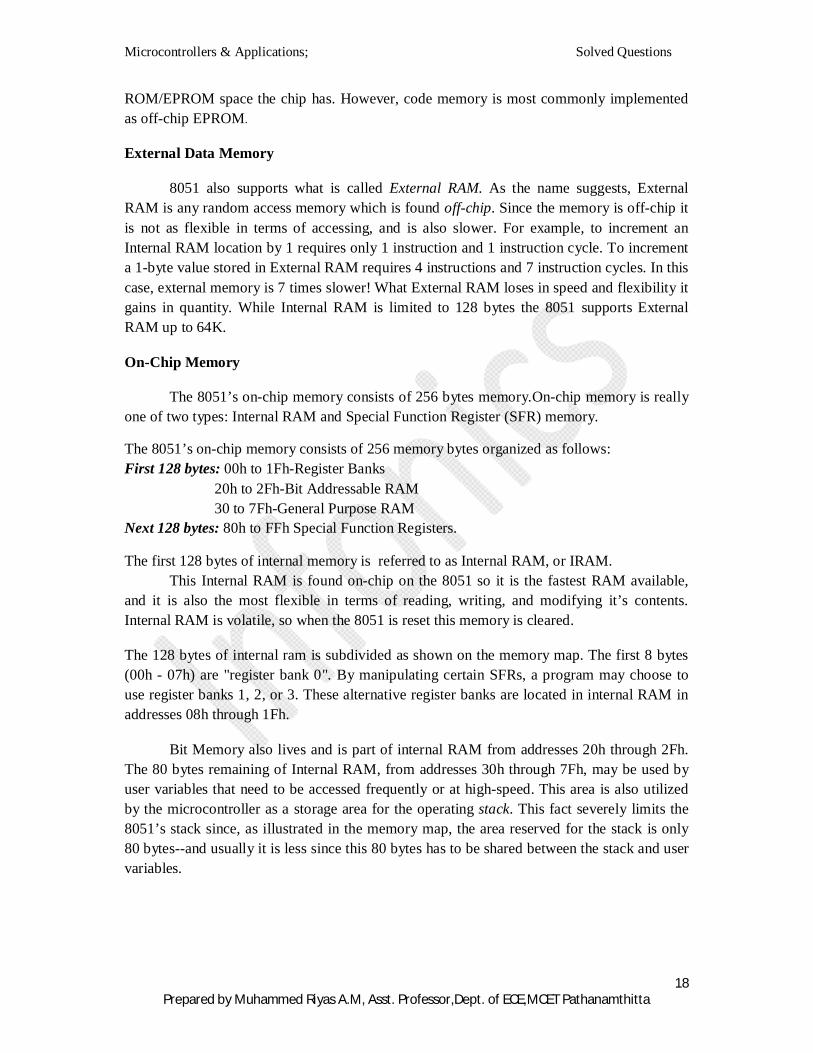
External Data Memory
8051 also supports what is called External RAM. As the name suggests, External RAM is any random access memory which is found off-chip. Since the memory is off-chip it is not as flexible in terms of accessing, and is also slower. For example, to increment an Internal RAM location by 1 requires only 1 instruction and 1 instruction cycle. To increment a 1-byte value stored in External RAM requires 4 instructions and 7 instruction cycles. In this case, external memory is 7 times slower! What External RAM loses in speed and flexibility it gains in quantity. While Internal RAM is limited to 128 bytes the 8051 supports External RAM up to 64K.
On-Chip Memory
The 8051’s on-chip memory consists of 256 bytes memory.On-chip memory is really one of two types: Internal RAM and Special Function Register (SFR) memory.
The 8051’s on-chip memory consists of 256 memory bytes organized as follows: First 128 bytes: 00h to 1Fh-Register Banks
20h to 2Fh-Bit Addressable RAM 30 to 7Fh-General Purpose RAM
Next 128 bytes: 80h to FFh Special Function Registers.
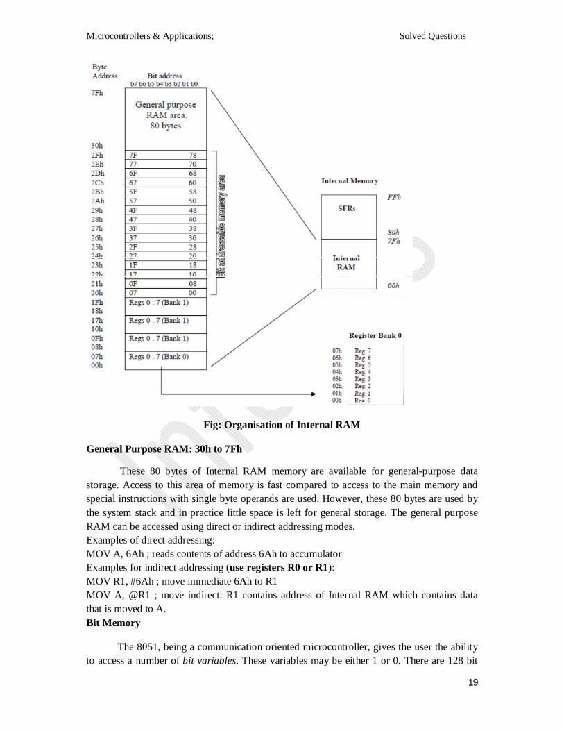
The first 128 bytes of internal memory is referred to as Internal RAM, or IRAM. This Internal RAM is found on-chip on the 8051 so it is the fastest RAM available,
and it is also the most flexible in terms of reading, writing, and modifying it’s contents. Internal RAM is volatile, so when the 8051 is reset this memory is cleared.
The 128 bytes of internal ram is subdivided as shown on the memory map. The first 8 bytes (00h - 07h) are "register bank 0". By manipulating certain SFRs, a program may choose to use register banks 1, 2, or 3. These alternative register banks are located in internal RAM in addresses 08h through 1Fh.
Bit Memory also lives and is part of internal RAM from addresses 20h through 2Fh. The 80 bytes remaining of Internal RAM, from addresses 30h through 7Fh, may be used by user variables that need to be accessed frequently or at high-speed. This area is also utilized by the microcontroller as a storage area for the operating stack. This fact severely limits the 8051’s stack since, as illustrated in the memory map, the area reserved for the stack is only 80 bytes--and usually it is less since this 80 bytes has to be shared between the stack and user variables.
Microcontrollers & Applications; Solved Questions
19
Fig: Organisation of Internal RAM
General Purpose RAM: 30h to 7Fh
These 80 bytes of Internal RAM memory are available for general-purpose data storage. Access to this area of memory is fast compared to access to the main memory and special instructions with single byte operands are used. However, these 80 bytes are used by the system stack and in practice little space is left for general storage. The general purpose RAM can be accessed using direct or indirect addressing modes. Examples of direct addressing: MOV A, 6Ah ; reads contents of address 6Ah to accumulator Examples for indirect addressing (use registers R0 or R1): MOV R1, #6Ah ; move immediate 6Ah to R1 MOV A, @R1 ; move indirect: R1 contains address of Internal RAM which contains data that is moved to A. Bit Memory
The 8051, being a communication oriented microcontroller, gives the user the ability to access a number of bit variables. These variables may be either 1 or 0. There are 128 bit

Microcontrollers & Applications; Solved Questions
20 Prepared by Muhammed Riyas A.M, Asst. Professor,Dept. of ECE,MCET Pathanamthitta
variables available to the user, numbered 00h through 7Fh. The user may make use of these variables with commands such as SETB and CLR. It is important to note that Bit Memory is really a part of Internal RAM. In fact, the 128 bit variables occupy the 16 bytes of Internal RAM from 20h through 2Fh.
Thus, if you write the value FFh to Internal RAM address 20h you’ve effectively set bits 00h through 07h. But since the 8051 provides special instructions to access these 16 bytes of memory on a bit by bit basis it is useful to think of it as a separate type of memory. However, always keep in mind that it is just a subset of Internal RAM and that operations performed on Internal RAM can change the values of the bit variables.
Register Banks
The 8051 uses 8 "R" registers which are used in many of its instructions. These "R" registers are numbered from 0 through 7 (R0, R1, R2, R3, R4, R5, R6, and R7). These registers are generally used to assist in manipulating values and moving data from one memory location to another. For example, to add the value of R4 to the Accumulator, we would execute the following instruction: ADD A,R4
However, as the memory map shows, the "R" Register R4 is really part of Internal RAM. Specifically, R4 is address 04h. The above instruction accomplishes the same thing as the following operation: ADD A,04h
This instruction adds the value found in Internal RAM address 04h to the value of the Accumulator, leaving the result in the Accumulator. Since R4 is really Internal RAM 04h, the above instruction effectively accomplished the same thing.
But the 8051 has four distinct register banks. When the 8051 is first booted up, register bank 0 (addresses 00h through 07h) is used by default. However, your program may instruct the 8051 to 4 use one of the alternate register banks; i.e., register banks 1, 2, or 3. In this case, R4 will no longer be the same as Internal RAM address 04h. For example, if your program instructs the 8051 to use register bank 3, "R" register R4 will now be synonomous with Internal RAM address 1Ch.
Special Function Register (SFR) Memory
Special Function Registers (SFRs) are areas of memory that control specific functionality of the 8051 processor. For example, four SFRs permit access to the 8051’s 32 input/output lines. Another SFR allows a program to read or write to the 8051’s serial port. Other SFRs allow the user to set the serial baud rate, control and access timers, and configure the 8051’s interrupt system.
SFRs are accessed as if they were normal Internal RAM. The only difference is that Internal RAM is from address 00h through 7Fh whereas SFR registers exist in the address range of 80h through FFh.
Each SFR has an address (80h through FFh) and a name.Although the address range of 80h through FFh offer 128 possible addresses, there are only 21 SFRs in a standard 8051.

Microcontrollers & Applications; Solved Questions
21
All other addresses in the SFR range (80h through FFh) are considered invalid. Writing to or reading from these registers may produce undefined values or behavior.
Fig: Special Function Registers
Port Registers SFR
The standard 8051 has four 8 bit I/O ports: P0, P1, P2 and P3.
For example Port 0 is a physical 8 bit I/O port on the 8051. Read (input) and write (output) access to this port is done in software by accessing the SFR P0 register which is located at address 80h. SFR P0 is also bit addressable. Each bit corresponds to a physical I/O pin on the 8051. Example access to port 0:
SETB P0.7 ; sets the MSB bit of Port 0
CLR P0.7 ; clears the MSB bit of Port 0
The operand P0.7 uses the dot operator and refers to bit 7 of SFR P0. The same bit could be addressed by accessing bit location 87h. Thus the following two instructions have the same meaning:
CLR P0.7
Microcontrollers & Applications; Solved Questions
22
CLR 87h
Program Status Word (PSW)
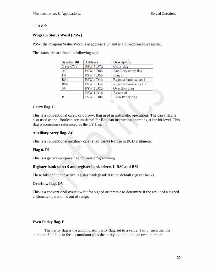
PSW, the Program Status Word is at address D0h and is a bit-addressable register.
The status bits are listed in following table.
Carry flag. C
This is a conventional carry, or borrow, flag used in arithmetic operations. The carry flag is also used as the ‘Boolean accumulator’ for Boolean instruction operating at the bit level. This flag is sometimes referenced as the CY flag.
Auxiliary carry flag. AC
This is a conventional auxiliary carry (half carry) for use in BCD arithmetic.
Flag 0. F0
This is a general-purpose flag for user programming.
Register bank select 0 and register bank selects 1. RS0 and RS1
These bits define the active register bank (bank 0 is the default register bank).
Overflow flag. OV
This is a conventional overflow bit for signed arithmetic to determine if the result of a signed arithmetic operation is out of range.
Even Parity flag. P
The parity flag is the accumulator parity flag, set to a value, 1 or 0, such that the number of ‘1’ bits in the accumulator plus the parity bit add up to an even number.

Microcontrollers & Applications; Solved Questions
23 Prepared by Muhammed Riyas A.M, Asst. Professor,Dept. of ECE,MCET Pathanamthitta
Stack Pointer
The Stack Pointer, SP, is an 8-bit SFR register at address 81h. The small address field (8 bits) and the limited space available in the Internal RAM confines the stack size and this is sometimes a limitation for 8051 programmes. The SP contains the address of the data byte currently on the top of the stack. The SP pointer in initialised to a defined address. A new data item is ‘pushed’ on to the stack using a PUSH instruction which will cause the data item to be written to address SP + 1. Typical instructions, which cause modification to the stack are: PUSH, POP, LCALL, RET, RETI etc.. The SP SFR, on start-up, is initialised to 07h so this means the stack will start at 08h and expand upwards in Internal RAM. If register banks 1 to 3 are to be used the SP SFR should be initialised to start higher up in Internal RAM. The following instruction is often used to initialise the stack:
MOV SP, #2Fh
Data Pointer
The Data Pointer, DPTR, is a special 16-bit register used to address the external code or external data memory. Since the SFR registers are just 8-bits wide the DPTR is stored in two SFR registers, where DPL (82h) holds the low byte of the DPTR and DPH (83h) holds the high byte of the DPTR. For example, if you wanted to write the value 46h to external data memory location 2500h, you might use the following instructions:
MOV A, #46h ; Move immediate 8 bit data 46h to A (accumulator)
MOV DPTR, #2504h ; Move immediate 16 bit address value 2504h to A.
; Now DPL holds 04h and DPH holds25h.
MOVX @DPTR, A ; Move the value in A to external RAM location 2500h.
Uses indirect addressing.
Note the MOVX (Move X) instruction is used to access external memory.
Accumulator
This is the conventional accumulator that one expects to find in any computer, which is used to the hold result of various arithmetic and logic operations. Since the 8051 microcontroller is just an 8-bit device, the accumulator is, as expected, an 8 bit register.
The accumulator, referred to as ACC or A, is usually accessed explicitly using instructions such as:
INC A ; Increment the accumulator
However, the accumulator is defined as an SFR register at address E0h. So the following two instructions have the same effect:

Microcontrollers & Applications; Solved Questions
24 Prepared by Muhammed Riyas A.M, Asst. Professor,Dept. of ECE,MCET Pathanamthitta
MOV A, #52h ; Move immediate the value 52h to the accumulator
MOV E0h, #52h ; Move immediate the value 52h to Internal RAM location E0h, which is, in fact, the accumulator SFR register.
Usually the first method, MOV A, #52h, is used as this is the most conventional (and happens to use less space, 2 bytes as oppose to 3 bytes!)
B Register
The B register is an SFR register at addresses F0h which is bit-addressable. The B register is used in two instructions only: i.e. MUL (multiply) and DIV (divide). The B register can also be used as a general-purpose register.
Program Counter
The PC (Program Counter) is a 2 byte (16 bit) register which always contains the memory address of the next instruction to be executed. When the 8051 is reset the PC is always initialised to 0000h. If a 2 byte instruction is executed the PC is incremented by 2 and if a 3 byte instruction is executed the PC is incremented by three so as to correctly point to the next instruction to be executed. A jump instruction (e.g. LJMP) has the effect of causing the program to branch to a newly specified location, so the jump instruction causes the PC contents to change to the new address value.
SFR Registers for the Internal Timer
The set up and operation of the on-chip hardware timers will be described later, but the associated registers are briefly described here:
TCON, the Timer Control register is an SFR at address 88h, which is bit-addressable. TCON is used to configure and monitor the 8051 timers. The TCON SFR also contains some interrupt control bits, described later.
TMOD, the Timer Mode register is an SFR at address 89h and is used to define the operational modes for the timers, as will be described later.
TL0 (Timer 0 Low) and TH0 (Timer 0 High) are two SFR registers addressed at 8Ah and 8Bh respectively. The two registers are associated with Timer 0.
TL1 (Timer 1 Low) and TH1 (Timer 1 High) are two SFR registers addressed at 8Ch and 8Dh respectively. These two registers are associated with Timer 1.
Power Control Register
Microcontrollers & Applications; Solved Questions
25 Prepared by Muhammed Riyas A.M, Asst. Professor,Dept. of ECE,MCET Pathanamthitta
PCON (Power Control) register is an SFR at address 87h. It contains various control bits including a control bit, which allows the 8051 to go to ‘sleep’ so as to save power when not in immediate use.
Serial Port Registers
Programming of the on-chip serial communications port will be described later. The associated SFR registers, SBUF and SCON, are briefly introduced here, as follows:
The SCON (Serial Control) is an SFR register located at addresses 98h, and it is bit addressable.
SCON configures the behaviour of the on-chip serial port, setting up parameters such as the baud rate of the serial port, activating send and/or receive data, and setting up some specific control flags.
The SBUF (Serial Buffer) is an SFR register located at address 99h. SBUF is just a single byte deep buffer used for sending and receiving data via the on-chip serial port.
Interrupt Registers
Interrupts will be discussed in more detail later. The associated SFR registers are: IE (Interrupt Enable) is an SFR register at addresses A8h and is used to enable and disable specific interrupts. The MSB bit (bit 7) is used to disable all interrupts.
IP (Interrupt Priority) is an SFR register at addresses B8h and it is bit addressable.
The IP register specifies the relative priority (high or low priority) of each interrupt. On the 8051, an interrupt may either be of low (0) priority or high (1) priority.
2. Explain the various addressing modes of 8051 with examples. OR Explain different addressing modes used in 8051 microcontroller (Nov 2006)
ANS:
Addressing mode is a way to address an operand. Operand means the data we are operating
upon (in most cases source data). It can be a direct address of memory, it can be register
names, it can be any numerical data etc.
Immediate Addressing Mode
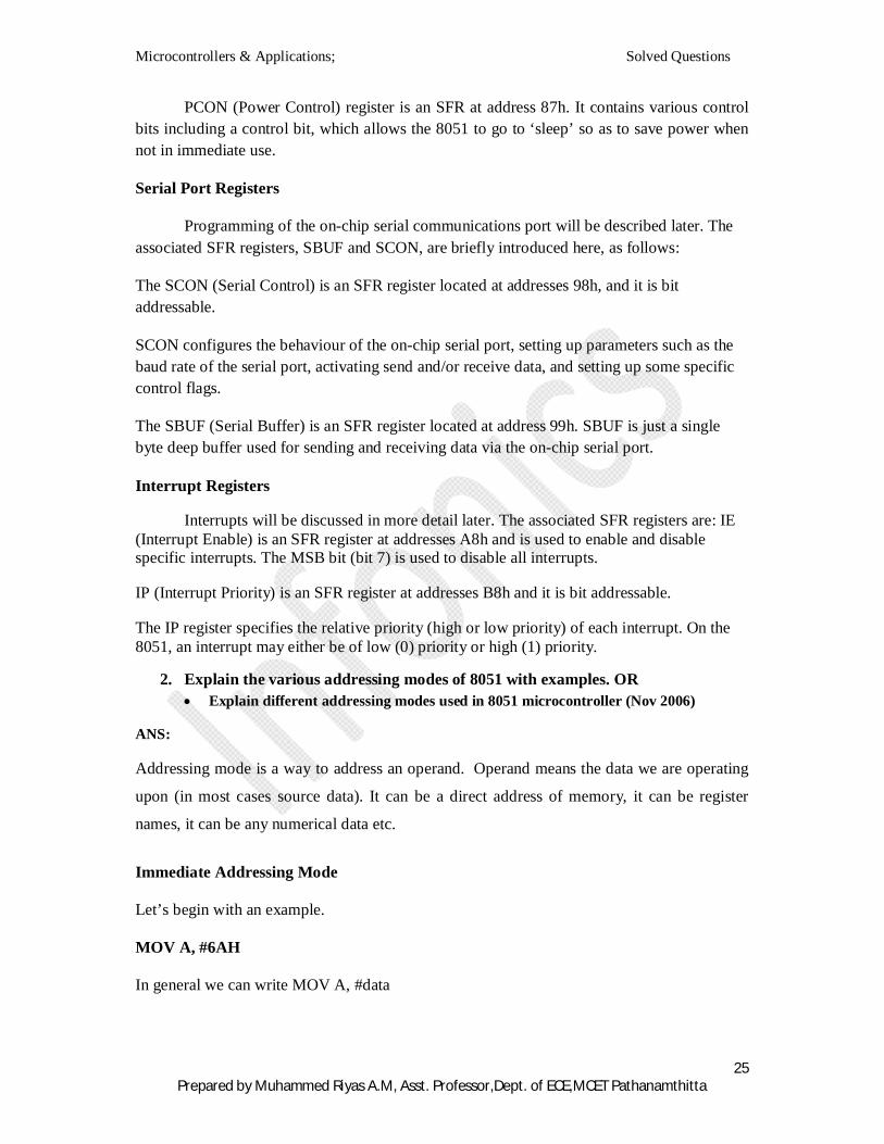
Let’s begin with an example.
MOV A, #6AH
In general we can write MOV A, #data
Microcontrollers & Applications; Solved Questions
26
This addressing mode is named as “immediate” because it transfers an 8-bit data immediately to the accumulator (destination operand).
The opcode for MOV A, # data is 74H. The opcode is saved in program memory at 0202 address. The data 6AH is saved in program memory 0203. (See, any part of the program memory can be used, this is just an example) When the opcode 74H is read, the next step taken would be to transfer whatever data at the next program memory address (here at 0203) to accumulator A (E0H is the address of accumulator). This instruction is of two bytes and is executed in one cycle. So after the execution of this instruction, program counter will add 2 and move to o204 of program memory.
Direct Addressing Mode
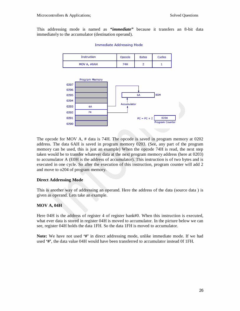
This is another way of addressing an operand. Here the address of the data (source data ) is given as operand. Lets take an example.
MOV A, 04H
Here 04H is the address of register 4 of register bank#0. When this instruction is executed, what ever data is stored in register 04H is moved to accumulator. In the picture below we can see, register 04H holds the data 1FH. So the data 1FH is moved to accumulator.
Note: We have not used ‘#’ in direct addressing mode, unlike immediate mode. If we had used ‘#’, the data value 04H would have been transferred to accumulator instead 0f 1FH.
Microcontrollers & Applications; Solved Questions
27
As shown in figure above this is a 2 byte instruction which requires 1 cycle to complete. Program counter will increment by 2 and stand in 0204. The opcode for instruction MOV A, address is E5H. When the instruction at 0202 is executed (E5H), accumulator is made active and ready to receive data. Then program control goes to next address that is 0203 and look up the address of the location (04H) where the source data (to be transferred to accumulator) is located. At 04H the control finds the data 1F and transfers it to accumulator and hence the execution is completed.
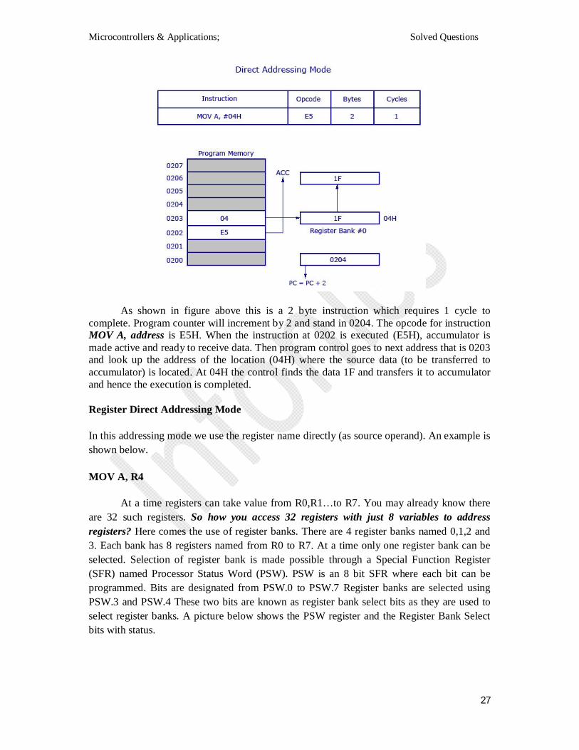
Register Direct Addressing Mode
In this addressing mode we use the register name directly (as source operand). An example is shown below.
MOV A, R4
At a time registers can take value from R0,R1…to R7. You may already know there are 32 such registers. So how you access 32 registers with just 8 variables to address registers? Here comes the use of register banks. There are 4 register banks named 0,1,2 and 3. Each bank has 8 registers named from R0 to R7. At a time only one register bank can be selected. Selection of register bank is made possible through a Special Function Register (SFR) named Processor Status Word (PSW). PSW is an 8 bit SFR where each bit can be programmed. Bits are designated from PSW.0 to PSW.7 Register banks are selected using PSW.3 and PSW.4 These two bits are known as register bank select bits as they are used to select register banks. A picture below shows the PSW register and the Register Bank Select bits with status.

Microcontrollers & Applications; Solved Questions
28
So in register direct addressing mode, data is transferred to accumulator from the register (based on which register bank is selected).
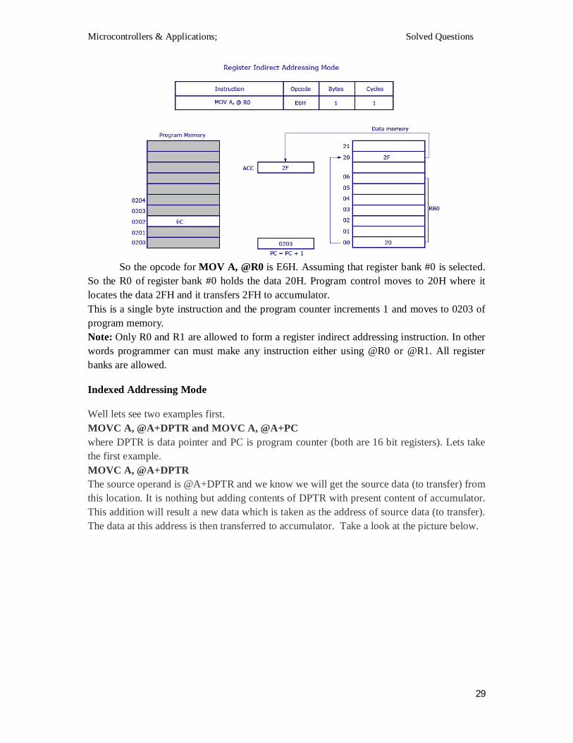
Register Indirect Addressing Mode In this addressing mode, address of the data (source data to transfer) is given in the
register operand. MOV A, @R0 Here the value inside R0 is considered as an address, which holds the data to be transferred to accumulator. Example: If R0 holds the value 20H, and we have a data 2F H stored at the address 20H, then the value 2FH will get transferred to accumulator after executing this instruction.
Microcontrollers & Applications; Solved Questions
29
So the opcode for MOV A, @R0 is E6H. Assuming that register bank #0 is selected.
So the R0 of register bank #0 holds the data 20H. Program control moves to 20H where it locates the data 2FH and it transfers 2FH to accumulator. This is a single byte instruction and the program counter increments 1 and moves to 0203 of program memory. Note: Only R0 and R1 are allowed to form a register indirect addressing instruction. In other words programmer can must make any instruction either using @R0 or @R1. All register banks are allowed.
Indexed Addressing Mode
Well lets see two examples first. MOVC A, @A+DPTR and MOVC A, @A+PC where DPTR is data pointer and PC is program counter (both are 16 bit registers). Lets take the first example. MOVC A, @A+DPTR The source operand is @A+DPTR and we know we will get the source data (to transfer) from this location. It is nothing but adding contents of DPTR with present content of accumulator. This addition will result a new data which is taken as the address of source data (to transfer). The data at this address is then transferred to accumulator. Take a look at the picture below.

Microcontrollers & Applications; Solved Questions
30
The opcode for the instruction is 93H. DPTR holds the value 01FE, where 01 is
located in DPH (higher 8 bits) and FE is located in DPL (lower 8 bits). Accumulator now has the value 02H. A 16 bit addition is performed and now 01FE H+02 H results in 0200 H. What ever data is in 0200 H will get transferred to accumulator. The previous value inside accumulator (02H) will get replaced with new data from 0200H. New data in the accumulator is shown in dotted line box.

Microcontrollers & Applications; Solved Questions
31
MODULE-3
Short Answer Questions
1. Name the five interrupt sources of 8051? ANS:
There are five interrupt sources for the 8051. Since the main RESET input can also be considered as an interrupt, six interrupts can be listed as follows:
2. Assume that XTAL = 11.0592 MHz, write a program to generate a square wave of 2 kHz frequency on pin P1.5.
Solution:
Look at the following steps. (a) T = 1 / f = 1 / 2 kHz = 500 us the period of square wave. (b) 1 / 2 of it for the high and low portion of the pulse is 250 us. (c) 250 us / 1.085 us = 230 and 65536 – 230 = 65306 which in hex is FF1AH. (d) TL = 1A and TH = FF, all in hex.
Program
MOV TMOD,#01 ;Timer 0, 16-bitmode AGAIN: MOV TL1,#1AH ;TL1=1A, low byte of timer MOV TH1,#0FFH ;TH1=FF, the high byte SETB TR1 ;Start timer 1 BACK: JNB TF1,BACK ;until timer rolls over CLR TR1 ;Stop the timer 1 CLR P1.5 ;Clear timer flag 1 CLR TF1 ;Clear timer 1 flag SJMP AGAIN ;Reload timer
3. Program the 8051 to receive bytes of data serially, and put them in PI. Set the baud rate at 4800, 8-bit data, and 1 stop bit.

Microcontrollers & Applications; Solved Questions
32
Essay Questions
1. Explain the interrupt structure of 8051 microcontroller Explain how interrupts are prioritized.
Ans:
Figure shows the set of 8051 interrupt sources. If we follow the external interrupt INT0, for example, we see that this external interrupt connects to the processor at the P3.2 pin. Note Port 3 can be used as a standard input/output port as shown earlier – but various Port 3 pins have alternative functionality. When INT0 is activated (negative edge usually), internally within the 8051 the EX0 request is raised. This flags an interrupt request but the relevant interrupt bit within the IE register must be set, along with the EA bit if this interrupt request is to raise an interrupt flag. The interrupt flag IE0 is then raised and causes the program counter (PC) to vector to vector location 0003h, as discussed earlier. Note, the Timer/Counter interrupt flags can be software polled even if the ETx bits are not enabled. Interrupts can also be software generated by setting the interrupt flags in software. The interrupt flags are accessible as flags on the TCON and SCON registers as follows:

Microcontrollers & Applications; Solved Questions
33
Fig: Interrupt sources
2. Give different steps followed by 8051 in response to interrupt. Explain with an example.
ANS:
Upon activation of an interrupt, the microcontroller goes through the following steps;
1. It finishes the instruction it is executing and saves the address of the next instruction (PC) on the stack.
2. It also saves the current status of all the inrterrupts internally.
3. It jumps to a fixed location in the memory called the interrupt vector table that holds the address of the interrupt service routine.
4. The microcontroller gets the address of the ISR from the interrupt vector table and jumps to it. It starts to execute the interrupt service routine until it reaches the last instruction of the subroutine, which is RETI (return from interrupt).
5. Upon executing the RETI instruction, the microcontroller returns to the place where it was interrupted. First, it gets the program counter (PC) address from the stack by popping the top two bytes of the stack in to the PC. Then it starts to execute from that address.
The following figure shows the flow of operation when a system is interrupted.
Microcontrollers & Applications; Solved Questions
34
Fig: Interrupt Operation Example.
In this example it is assumed that some program, say the main program, is executing when the external interrupt INT0 occurs. The 8051 hardware will automatically complete the current machine level (assembler level) instruction and save the Program Counter to the stack. The IE register is also saved to the stack. The IE0 flag is disabled (cleared) so that another INT0 interrupt will be inhibited while the current interrupt is being serviced. The Program Counter is now loaded with the vector location 0003h. This vector address is a predefined address for interrupt INT0 so that program execution will always trap to this address when an INT0 interrupt occurs. Other interrupt sources have uniquely defined vector
Microcontrollers & Applications; Solved Questions
35
addresses for this purpose. The set of these vector addresses is referred to as the interrupt vector table.
Program execution is now transferred to address location 0003h. In the example a LJMP instruction is programmed at this address to cause the program to jump to a predefined start address location for the relevant ISR (Interrupt Service Routine) routine. The ISR routine is a user written routine, which defines what action is to occur following the interrupt event. It is good practice to save (PUSH) to the stack any registers used during the ISR routine and to restore (POP) these registers at the end of the ISR routine, thus preserving the registers’ contents, just like a register is preserved within a subroutine program. The last instruction in the ISR routine is a RETI (RETurn from Interrupt) instruction and this instruction causes the 8051 to restore the IE register values, enable the INT0 flag, and restore the Program Counter contents from the stack.
Since the Program Counter now contains the address of the next instruction which was to be executed before the INT0 interrupt occurred, the main program continues as if it had never being interrupted. Thus only the temporal behaviour of the interrupted program has been affected by the interrupt; the logic of the program has not been otherwise affected.
3. What is a Timer? Write a short note on Timer modes of operation.OR
Explain the timer modes of operation of 8051 in detail.
ANS:
Timer is a clock that controls the sequence of an event while counting in fixed intervals of time. A Timer is used for producing precise time delay. Secondly, it can be used to repeat or initiate an action after/at a known period of time.
Different modes of a Timer
There are four Timer modes designated as Modes 0, 1, 2 and 3. A particular mode is selected by configuring the M1 & M0 bits of TMOD register.
13-bit Time Mode (mode 0)
Mode 0 is a 13 bit Timer mode and uses 8 bits of high byte and 5 bit prescaler of low byte. The value that the Timer can update in mode0 is from 0000H to 1FFFH. The 5 bits of

Microcontrollers & Applications; Solved Questions
36 Prepared by Muhammed Riyas A.M, Asst. Professor,Dept. of ECE,MCET Pathanamthitta
lower byte append with the bits of higher byte. The Timer rolls over from 1FFFH to 0000H to raise the Timer flag.
Timer mode "0" is a 13-bit timer. This is a relic that was kept around in the 8051 to maintain compatability with its predecesor, the 8048. Generally the 13-bit timer mode is not used in new development. When the timer is in 13-bit mode, TLx will count from 0 to 31. When TLx is incremented from 31, it will "reset" to 0 and increment THx. Thus, effectively, only 13 bits of the two timer bytes are being used: bits 0-4 of TLx and bits 0-7 of THx. This also means, in essence, the timer can only contain 8192 values. If you set a 13-bit timer to 0, it will overflow back to zero 8192 machine cycles later.
16-bit Time Mode (mode 1)
Mode1 is one of the most commonly used Timer modes. It allows all 16 bits to be used for the Timer and so it allows values to vary from 0000H to FFFFH.
If a value, say YYXXH, is loaded into the Timer bytes, then the delay produced by the Timer will be equal to the product :
[ ( FFFFH – YYXXH +1 ) x ( period of one timer clock ) ].
It can also be considered as follows: convert YYXXH into decimal, say NNNNN, then delay will be equal to the product : [ ( 65536-NNNNN ) x ( period of one timer clock ) ].
The period of one timer clock is 1.085 μs for a crystal of 11.0592 MHz frequency as discussed above. Timer mode "1" is a 16-bit timer. This is a very commonly used mode. It functions just like 13-bit mode except that all 16 bits are used.
TLx is incremented from 0 to 255. When TLx is incremented from 255, it resets to 0 and causes THx to be incremented by 1. Since this is a full 16-bit timer, the timer may contain up to 65536 distinct values. If you set a 16-bit timer to 0, it will overflow back to 0 after 65,536 machine cycles.
8-bit Time Mode (mode 2)
Timer mode "2" is an 8-bit auto-reload mode. What is that, you may ask? Simple. When a timer is in mode 2, THx holds the "reload value" and TLx is the timer itself. Thus, TLx starts counting up. When TLx reaches 255 and is subsequently incremented, instead of resetting to 0 (as in the case of modes 0 and 1), it will be reset to the value stored in THx. For example, let us say TH0 holds the value FDh and TL0 holds the value FEh. If we were to watch the values of TH0 and TL0 for a few machine cycles this is what we see:

Microcontrollers & Applications; Solved Questions
37
As you can see, the value of TH0 never changed. In fact, when you use mode 2 you almost always set THx to a known value and TLx is the SFR that is constantly incremented. Whats the benefit of auto-reload mode? Perhaps you want the timer to always have a value from 200 to 255. If you use mode 0 or 1, you have to check in code to see if the timer had overflowed and, if so, reset the timer to 200. This takes precious instructions of execution time to check the value and/or to reload it. When you use mode 2 the microcontroller takes care of this for you. Once you have configured a timer in mode 2 you dont have to worry about checking to see if the timer has overflowed nor do you have to worry about resetting the value--the microcontroller hardware will do it all for you. The auto-reload mode is very commonly used for establishing a baud rate.
Split Timer Mode (mode 3)
Timer mode "3" is a split-timer mode. When Timer 0 is placed in mode 3, it essentially becomes two separate 8-bit timers. That is to say, Timer 0 is TL0 and Timer 1 is TH0. Both timers count from 0 to 255 and overflow back to 0. All the bits that are related to Timer 1 will now be tied to TH0.
While Timer 0 is in split mode, the real Timer 1 (i.e. TH1 and TL1) can be put into modes 0, 1 or 2 normally--however, you may not start or stop the real timer 1 since the bits that do that are now linked to TH0. The real timer 1, in this case, will be incremented every machine cycle no matter what.
4. Write a program in which the 8051 gets data from P1 and sends it to P2 continuously while incoming data from the serial port is sent to P0. Assume that XTAL=11.0592. Set the baud rata at 9600.

Microcontrollers & Applications; Solved Questions
38 Prepared by Muhammed Riyas A.M, Asst. Professor,Dept. of ECE,MCET Pathanamthitta
Solution:
ORG 0 LJMP MAIN
; ------ main program, initialization ------
MAIN: MOV P1,#OFFH ;make P1 an input port MOV TMOD,#20H ;timer 1,mode 2 (auto reload) MOV TH1,#OFDH ;9600 baud rate MOV SCON,#50H ;8-bit, 1 stop, REN enabled SETB TR1 ;start timer 1
BACK: MOV A,P1 MOV P2,A MOV SBUF,A ;A has a copy of data HERE: JNB TI,HERE ;jump if TI is high CLR TI SJMP BACK END
5 .Write a program in which the 8051 gets data from P1 and sends it to P2 continuously while incoming data from the serial port is sent to P0. Assume that XTAL = 11.0592. Set the baud rate at 9600.
Solution
ORG 0
; ------ main program, initialization ------
MAIN: MOV P1,#0FFH ;make P1 an input port MOV TMOD,#20H ;timer 1, mode 2 (auto reload) MOV TH1,#OFDH ;9600 baud rate MOV SCON,#50H ;8-bit,1 stop, REN enabled SETB TR1 ;start timer 1
BACK: MOV A,P1 MOV P2,A HERE: JNB RI,HERE MOV A,SBUF MOV P0,A CLR RI SJMP BACK END

Microcontrollers & Applications; Solved Questions
39
6. Which are the different serial communication modes.Explain.
Serial Communication: Different modes
o Mode - 0 Shift register mode.
Serial data enters and exists through RXD. 8-bits are transmitted/recieved. Pin TXD is connected to the internal shift frequency pulse source to supply shift pulses to external circuits. The shift frequency or baud rate is fixed at 1/2 of the oscillator frequency.
o Mode - 1 Standard UART
10 bits are transmitted (through TXD) or recieved through (RXD), a start bit(0), 8 data bits (LSB first), and a stop bit(1). Once recieved, the stop bits goes into RB8 in special function register SCON.The baud rate is variable.
o Mode - 2 Multiprocessor Mode.
11 bits are transmitted through TXD or recieved through RXD, a start bit (0), 8 data bits (LSB first), a programmable 9th bit and a stop bit(1). On transmission, the 9th data bit (TB8 in SCON) can be assigned the value 0 or 1. Or, for example, the parity bit (P in the PSN) could be moved into TB8. On receive, the 9th bit goes into RB8 in SFR SCON, which the stop bit is ignored. The bandwidth is programmable to either 1/32 or 1/64 of oscillator frequency.
o Mode - 3
11 bits are transmitted through TXD or received through RXD: a start bit, 8 data bits (LSB first), a programmable 9th bit, and a stop bit (1). In fact, Mode 3 is same as Mode 2 in all respects except the baud rate. The baud rate in Mode 3 is variable.

Microcontrollers & Applications; Solved Questions
40
Module-4
1. Explain interfacing of LED with 8051 micro controller.
2. Program 3. ORG 0000h 4. loop: 5. CLR P2.0 6. ACALL DELAY 7. SETB P2.0 8. ACALL DELAY 9. SJMP loop
2. Draw and explain the interfacing circuit of LCD with 8051.
Circuit diagram
3.
The circuit diagram given above shows how to interface a 16×2 LCD module with 8051 microcontroller. P1.0 to P1.7 pins of the microcontroller is connected to the D0 to D7 pins of the module respectively and through this route the data goes to the LCD module. P3.3, P3.4 and P3.5 are connected to the E, R/W, RS pins of the microcontroller and through this route the control signals are transffered to the LCD module. POT is used for adjusting the contrast of the display.
3.Give any four applications of relay circuits.

Microcontrollers & Applications; Solved Questions
41
Applications of Relay
Relays are used to realize logic functions. They play a very important role in providing
safety critical logic.
Relays are used to provide time delay functions. They are used to time the delay open and
delay close of contacts.
Relays are used to control high voltage circuits with the help of low voltage signals.
Similarly they are used to control high current circuits with the help of low current
signals.
They are also used as protective relays. By this function all the faults during transmission
and reception can be detected and isolated.
Essay Questions
1. Explain the interfacing of 7 segment LED display with 8051 microcontroller.
Microcontrollers & Applications; Solved Questions
42
Program
ORG 000H //initial starting address MOV A,#00H // set a count to point the address of each digit pattern NEXT: MOV R0,A MOV DPTR,#ARRAY MOVC A,@A+DPTR // Read the Digit drive pattern MOV P1,A // Move to the port for display ACALL DELAY // calls the delay MOV A,R0 // R0 INC A SJMP NEXT
SJMP $
ARRAY:DB 3FH // digit drive pattern for 0 DB 06H // digit drive pattern for 1 DB 5BH // digit drive pattern for 2 DB 4FH // digit drive pattern for 3 DB 66H // digit drive pattern for 4 DB 6DH // digit drive pattern for 5 DB 7DH // digit drive pattern for 6 DB 07H // digit drive pattern for 7 DB 7FH // digit drive pattern for 8 DB 6FH // digit drive pattern for 9 DELAY: MOV R2,#0FFH // subroutine for delay WAIT: DJNZ R2,WAIT RET END

Microcontrollers & Applications; Solved Questions
43
Program Description. Instruction MOVC A,@A+DPTR is the instruction that produces the required digit drive pattern for the display. Execution of this instruction will add the value in the accumulator A with the content of the data pointer (starting address of the ARRAY) and will move the data present in the resultant address to A. In the program, initial value in A is 00H. Execution of MOVC A,@A+DPTR will add 00H to the content in DPTR . The result will be the address of label DB 3FH and the data present in this address ie 3FH (digit drive pattern for 0) gets moved into the accumulator. Moving this pattern in the accumulator to Port 1 will display 0 which is the first count. At the next count, value in A will advance to 01H and after the execution of MOVC A,@+DPTR ,the value in A will be 06H which is the digit drive pattern for 1 and this will display 1 which is the next count and this cycle gets repeated for subsequent counts. Label DB is known as Define Byte – which defines a byte. This table defines the digit drive patterns for 7 segment display as bytes (in hex format). MOVC operator fetches the byte from this table based on the result of adding DPTR and contents in the accumulator. Register R0 is used as a temporary storage of the initial value of the accumulator and the subsequent increments made to accumulator to fetch each digit drive pattern one by one from the ARRAY.
2. Write a program to turns the lamp on and off by energizing and de-energizing the relay every second.
3. A switch is connected to pin P2.7. Write an ALP to monitor the status of the SW. If SW = 0, motor moves clockwise and if SW = 1, motor moves anticlockwise.
Microcontrollers & Applications; Solved Questions
44
Program:
ORG 0000H SETB P2.7 MOV A, #66H MOV P1,A
TURN: JNB P2.7, CW RL A
ACALL DELAY MOV P1,A SJMP TURN
CW: RR A ACALL DELAY MOV P1,A
SJMP TURN DELAY: MOV R1,#100 UP1: MOV R2,#50 UP: DJNZ R2,UP
DJNZ R1,UP1 RET
4. Explain the interfacing of ADC0804 with 8051 microcontroller.
Circuit Diagram

Microcontrollers & Applications; Solved Questions
45 Prepared by Muhammed Riyas A.M, Asst. Professor,Dept. of ECE,MCET Pathanamthitta
The figure above shows the schematic for interfacing ADC0804 to 8051. The circuit initiates the ADC to convert a given analogue input , then accepts the corresponding digital data and displays it on the LED array connected at P0. For example, if the analogue input voltage Vin is 5V then all LEDs will glow indicating 11111111 in binary which is the equivalent of 255 in decimal. AT89s51 is the microcontroller used here. Data out pins (D0 to D7) of the ADC0804 are connected to the port pins P1.0 to P1.7 respectively. LEDs D1 to D8 are connected to the port pins P0.0 to P0.7 respectively. Resistors R1 to R8 are current limiting resistors. In simple words P1 of the microcontroller is the input port and P0 is the output port. Control signals for the ADC (INTR, WR, RD and CS) are available at port pins P3.4 to P3.7 respectively. Resistor R9 and capacitor C1 are associated with the internal clock circuitry of the ADC. Preset resistor R10 forms a voltage divider which can be used to apply a particular input analogue voltage to the ADC. Push button S1, resistor R11 and capacitor C4 forms a debouncing reset mechanism. Crystal X1 and capacitors C2,C3 are associated with the clock circuitry of the microcontroller.
Program.
ORG 00H MOV P1,#0FFH // initiates P1 as the input port SETB P3.4 MAIN: CLR P3.7 // makes CS=0 SETB P3.6 // makes RD high CLR P3.5 // makes WR low SETB P3.5 // low to high pulse to WR for starting conversion WAIT: JB P3.4,WAIT // polls until INTR=0 CLR P3.7 // ensures CS=0 CLR P3.6 // high to low pulse to RD for reading the data from ADC MOV A,P1 // moves the digital data to accumulator CPL A // complements the digital data MOV P0,A // outputs the data to P0 for the LEDs SJMP MAIN // jumps back to the MAIN program END
5. Write a program to generate a sine wave using DAC 0808.
To generate a sine wave, we first need a table whose values represent the magnitude of the sine of angles between 0 and 360 degrees. The values for the sine function vary from -1.0 to +1.0 for 0- to 360-degree angles. Therefore, the table values are integer numbers representing the voltage magnitude for the sine of theta. This method ensures that only integer numbers are output to the DAC by the 8051 microcontroller. Table shows the angles, the sine values, the voltage magnitudes, and the integer values representing the voltage magnitude for each angle (with 30-degree increments). To generate Table, we assumed the full-scale voltage of 10 V for DAC output Full-scale output of the DAC is achieved when all
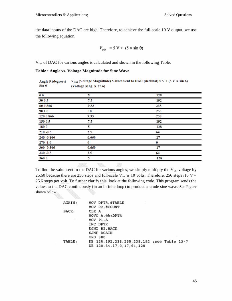
Microcontrollers & Applications; Solved Questions
46
the data inputs of the DAC are high. Therefore, to achieve the full-scale 10 V output, we use the following equation.
Vout of DAC for various angles is calculated and shown in the following Table.
Table : Angle vs. Voltage Magnitude for Sine Wave
To find the value sent to the DAC for various angles, we simply multiply the Vout voltage by 25.60 because there are 256 steps and full-scale Vout is 10 volts. Therefore, 256 steps /10 V = 25.6 steps per volt. To further clarify this, look at the following code. This program sends the values to the DAC continuously (in an infinite loop) to produce a crude sine wave. See Figure shown below.

Microcontrollers & Applications; Solved Questions
47

Microcontrollers & Applications; Solved Questions
48 Prepared by Muhammed Riyas A.M, Asst. Professor,Dept. of ECE,MCET Pathanamthitta
MODULE-5
Short Answer Questions
1. What are the feactures of PIC Microcontroller ?
Ans:
1. Parallel I/O ports 2. Timer functions, including counters, input capture, output compare, real-time interrupt, and watchdog timer 3. Pulse width modulation (PWM) 4. SPI and I2C serial interface 5. Universal Synchronous/Asynchronous Receiver Transmitter (USART) 6. A/D converter with 10-bit resolution 7. Analog comparator 8. Low-power operation mode 9. SRAM and EEPROM 10. EPROM or flash memory 11. Controller Area Network (CAN)
2. Briefly explain the CCP.
CCP stands for Capture/Compare/PWM.
The CCP module is a peripheral which allows the user to time and control different events.
Capture Mode, allows timing for the duration of an event. This circuit gives insight into the current state of a register which constantly changes its value. In this case, it is the timer TMR1 register.
Compare Mode compares values contained in two registers at some point. One of them is the timer TMR1 register. This circuit also allows the user to trigger an external event when a predetermined amount of time has expired.
PWM - Pulse Width Modulation can generate signals of varying frequency and duty cycle.
The PIC16F887 microcontroller has two such modules - CCP1 and CCP2.
Both of them are identical in normal mode, with the exception of the Enhanced PWM features available on CCP1 only. This is why this chapter describes the CCP1 module in detail. Concerning CCP2, only the features distinguishing it from CCP1 will be covered.
3. Briefly explain the sources of interrupt in PIC microcontroller.
External interrupts – they are named INTx (like INT0, INT1 etc), they provide a means for external hardware to generate interrupts. Like if you connect a touch screen controller to your PIC MCU. Then the touch screens PENINT (pen interrupt) can be connected to INT0 (or any other INTx). Then when ever the pen (or stylus) touches
Microcontrollers & Applications; Solved Questions
49
the screen it will interrupt the CPU. This interrupt will be explained in details in its own tutorial.
TIMER interrupts – They are also very common in MCUs. Today’s MCUs comes with very sophisticated timers that can do lots of magic for you. They have they related interrupts. In most simple situation they can act like alarm clocks that can interrupt the CPU at predefined intervals. If you toggle a i/o pin in response to these alarms (interrupts), what you have is a frequency generator! For more info on timers on PIC18, read this article.
Analog to Digital Converter Interrupts – A/D Converter takes some time to complete its operation. So the CPU can either wait for it to complete or set up an AD conversion complete interrupt. In the latter case CPU can do other tasks while A/D converter converts the input. As soon as A/D converter completes its job it will inform CPU to read the value from its buffer. For more info on A/D Converter of PIC18, read this article.
Data Interrupts – MCUs have many different types of data i/o engines, like USART, SPI, I2C, Parallel etc. They can also interrupt the CPU when data transmission is complete or data arrives from external source. Like an RFID reader send a packet because a user just brought his or her card near the reader. Or the GSM module detected an incoming call.
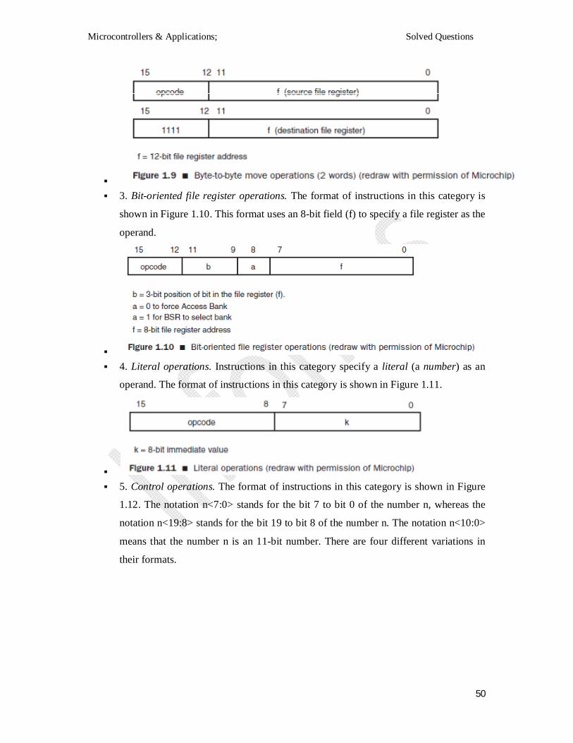
4. Explain the instruction format of PIC microcontroller.
The instruction set is grouped into five basic categories:
1. Byte-oriented operations. The format of byte-oriented instructions is shown in
Figure 1.8. The 6-bit field opcode specifies the operation to be performed by the
ALU.
2. Byte-to-byte operations (two-word). The format of the instruction in this category is
shown in Figure 1.9. There is only one instruction that uses this format: movff f1, f2.
This instruction allows one to move data from one file register to another.
Microcontrollers & Applications; Solved Questions
50
3. Bit-oriented file register operations. The format of instructions in this category is
shown in Figure 1.10. This format uses an 8-bit field (f) to specify a file register as the
operand.
4. Literal operations. Instructions in this category specify a literal (a number) as an
operand. The format of instructions in this category is shown in Figure 1.11.
5. Control operations. The format of instructions in this category is shown in Figure
1.12. The notation n<7:0> stands for the bit 7 to bit 0 of the number n, whereas the
notation n<19:8> stands for the bit 19 to bit 8 of the number n. The notation n<10:0>
means that the number n is an 11-bit number. There are four different variations in
their formats.
Microcontrollers & Applications; Solved Questions
51
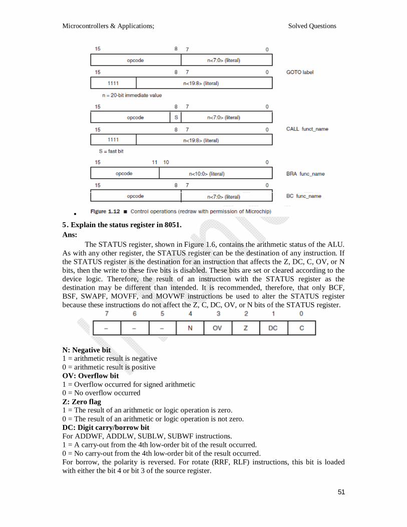
5 . Explain the status register in 8051. Ans:
The STATUS register, shown in Figure 1.6, contains the arithmetic status of the ALU. As with any other register, the STATUS register can be the destination of any instruction. If the STATUS register is the destination for an instruction that affects the Z, DC, C, OV, or N bits, then the write to these five bits is disabled. These bits are set or cleared according to the device logic. Therefore, the result of an instruction with the STATUS register as the destination may be different than intended. It is recommended, therefore, that only BCF, BSF, SWAPF, MOVFF, and MOVWF instructions be used to alter the STATUS register because these instructions do not affect the Z, C, DC, OV, or N bits of the STATUS register.
N: Negative bit 1 = arithmetic result is negative 0 = arithmetic result is positive OV: Overflow bit 1 = Overflow occurred for signed arithmetic 0 = No overflow occurred Z: Zero flag 1 = The result of an arithmetic or logic operation is zero. 0 = The result of an arithmetic or logic operation is not zero. DC: Digit carry/borrow bit For ADDWF, ADDLW, SUBLW, SUBWF instructions. 1 = A carry-out from the 4th low-order bit of the result occurred. 0 = No carry-out from the 4th low-order bit of the result occurred. For borrow, the polarity is reversed. For rotate (RRF, RLF) instructions, this bit is loaded with either the bit 4 or bit 3 of the source register.

Microcontrollers & Applications; Solved Questions
52
C: Carry/borrow bit For ADDWF, ADDLW, SUBLW, SUBWF instructions. 1 = A carry-out from the most significant bit of the result occurred. 0 = No carry-out from the most significant bit of the result has occurred. For borrow, the polarity is reversed. For rotate (RRF, RLF) instructions, this bit is loaded with either the high or low order bit of the source register. 6. Give comparison between CISC and RISC processors.
7.Explain data movement instructions in PIC 18 microcontroller.
Microcontrollers & Applications; Solved Questions
53
8.Explain addition and substraction instructions in PIC micro controller.
Ans:
Essay Questions
1. Explain the memory organization of PIC Micro controller.
Ans:
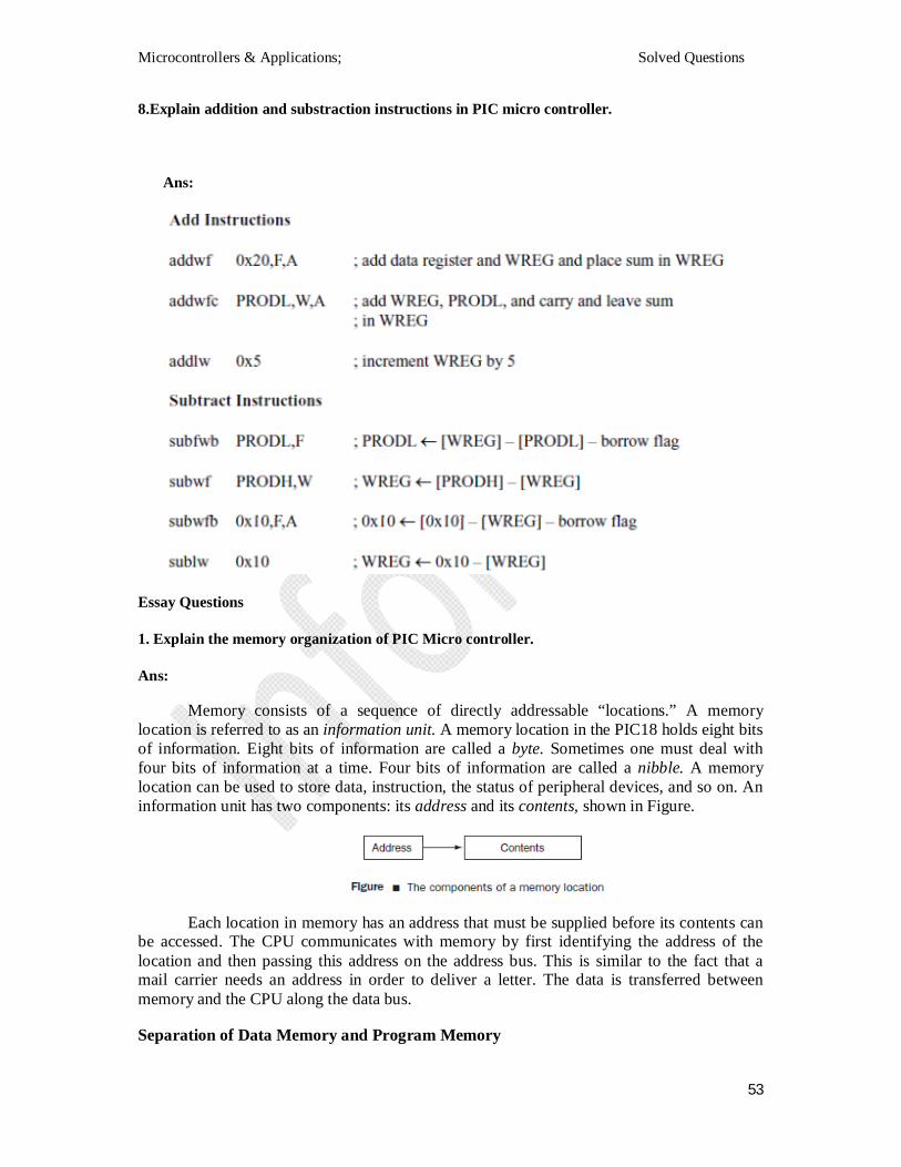
Memory consists of a sequence of directly addressable “locations.” A memory location is referred to as an information unit. A memory location in the PIC18 holds eight bits of information. Eight bits of information are called a byte. Sometimes one must deal with four bits of information at a time. Four bits of information are called a nibble. A memory location can be used to store data, instruction, the status of peripheral devices, and so on. An information unit has two components: its address and its contents, shown in Figure.
Each location in memory has an address that must be supplied before its contents can be accessed. The CPU communicates with memory by first identifying the address of the location and then passing this address on the address bus. This is similar to the fact that a mail carrier needs an address in order to deliver a letter. The data is transferred between memory and the CPU along the data bus.
Separation of Data Memory and Program Memory

Microcontrollers & Applications; Solved Questions
54
As shown in Figure, the PIC18 MCU assigns data and program to different memory spaces and provides separate buses to them so that both are available for access at the same time.
The PIC18 MCU has a 21-bit program counter that is divided into three registers: PCU, PCH, and PCL. Among them, only the PCL register is directly accessible to the user. Both the PCH and the PCL are eight bits, whereas the PCU is five bits.
Many digital systems have a large amount of memory. Therefore, special terms are often used to refer to the size of memory system. Among them, KB, MB, and GB are most often used:
_ 1 KB refers to 210 (1,024) bytes of memory.
_ 1 MB refers to 220 (1,048,576) bytes of memory.
_ 1 GB refers to 230 (1,073,741,824) bytes of memory.
PIC18 Data Memory
The PIC18 data memory is implemented as SRAM. Each location in the data memory is also referred to as a register or file register. The PIC18 MCU supports 4096 bytes of data memory. It requires 12 bits of address to select one of the data registers. The data memory map of the PIC18 MCU is shown in Figure.

Microcontrollers & Applications; Solved Questions
55
Because of the limited length of the PIC18 instruction (most instructions are 16 bits), only eight bits of the PIC18 instruction are used to specify the file register to be operated on. As a result, the PIC18 designers divided the 4096 file registers into 16 banks. Only one bank of 256 file registers is active at any time. An additional four bits are placed in a special register called bank select register (BSR) to select the bank to be active. The user needs to change the contents of the BSR register in order to change the active bank.
There are two types of registers: general-purpose registers (GPRs) and special-function registers (SFRs). GPRs are used to hold dynamic data when the PIC18 CPU is executing a program. SFRs are registers used by the CPU and peripheral modules for controlling the desired operation of the MCU. These registers are implemented as SRAM. The SFRs are assigned from the highest addresses and downward, whereas GPRs start from address 0 and upward. Depending on the device, some of the GPRs in the middle are not implemented.
For example, the PIC18F452 has 1536 (six banks) bytes of data memory, and then banks 0 to 5 and bank 15 are implemented. The first 96 bytes (in bank 0, 0x000-0x05F) of the GPRs and the last 160 bytes (in bank 15, 0xF60-0xFFF) of the SFRs are grouped into a special bank called access bank. The functioning of the access bank is explained in Section 1.8. For the PIC18F242/ 252/442/452 MCUs, the access bank comprises of the upper 128 bytes in bank 15 and the lower 128 bytes in bank 0.
EEPROM Data Memory
At the time of this writing, all the PIC18 devices that have on-chip flash program memory also have either 256 bytes or 1024 bytes of data EEPROM. The data EEPROM is readable and writable during normal operation over the entire power supply range. The data EEPROM memory is not directly mapped in the register file space. Instead, it is indirectly addressed through the special function register.

Microcontrollers & Applications; Solved Questions
56 Prepared by Muhammed Riyas A.M, Asst. Professor,Dept. of ECE,MCET Pathanamthitta
Program Memory Organization
Each PIC18 member has a 21-bit program counter and hence is capable of addressing the 2-MB program memory space. Accessing a nonexistent memory location will cause a read of all 0s. Different members of the PIC18 family have different memory configurations. The PIC18CXX2 and PIC18CXX8 devices have on-chip EPROM program memory only and cannot access external memory. The PIC18C601 and PIC18C801 do not have on-chip memory. The PIC18C601 is capable of accessing 256 KB of external program memory, whereas the PIC18C801 can access 2 MB of external program memory. The PIC18FXX2, PIC18FXX8, and the PIC18F6620/6720 devices have on-chip flash program memory only. The PIC18F8585/8680/8621/8620/8720 can also access external program memory in addition to their on-chip flash program memory.
The PIC18 MCU has a 31-entry return address stack that is used to hold return addresses for subroutine call and interrupt processing. This return address stack is not part of the program memory space. The program memory map is illustrated in Figure.
As shown in Figure, the address 000000h is assigned to the reset vector, which is the program-starting address after power-on or manual reset. The address 000008h is the starting address of the high-priority interrupt service routine. Sixteen bytes are allocated to the high-priority interrupt service routine by default. The address 000018h is the starting address for the low-priority interrupt service routine, and there is no default size for this service routine. The user program should follow the low-priority interrupt service routine.
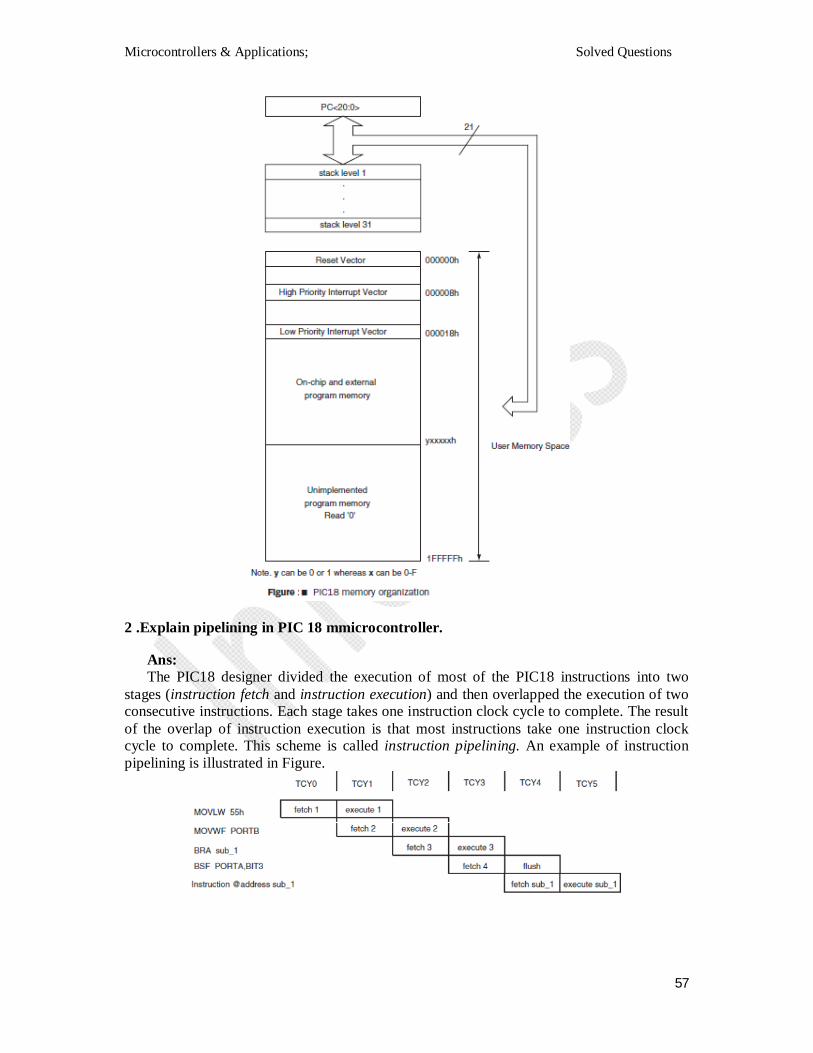
Microcontrollers & Applications; Solved Questions
57
2 .Explain pipelining in PIC 18 mmicrocontroller.
Ans: The PIC18 designer divided the execution of most of the PIC18 instructions into two
stages (instruction fetch and instruction execution) and then overlapped the execution of two consecutive instructions. Each stage takes one instruction clock cycle to complete. The result of the overlap of instruction execution is that most instructions take one instruction clock cycle to complete. This scheme is called instruction pipelining. An example of instruction pipelining is illustrated in Figure.

Microcontrollers & Applications; Solved Questions
58 Prepared by Muhammed Riyas A.M, Asst. Professor,Dept. of ECE,MCET Pathanamthitta
There are two problems caused by instruction pipelining: data dependency hazard and control hazard. In a program, it is common for one instruction to perform further operation on the result produced by the previous instruction. If the pipeline is designed in a way that the earlier instruction cannot write the result back to the register or memory location before it is used by the following instruction(s), then the data-dependency hazard has occurred. Most of the data dependency hazards can be solved by result forwarding. However, if an instruction reads from a memory location (e.g., a load instruction) whereas the following instruction will use the returned value to perform certain operation, then result forwarding cannot resolve the hazard. This problem is usually solved by rearranging the instruction sequence to avoid this type of data dependency or inserting a no-op instruction. The dependency hazard problem will occur on pipelined processors with more than two stages. The PIC18 instruction pipeline has only two stages and does not have data-dependency hazard problems.
Control hazard is caused by branch instructions. Whenever a branch instruction reaches the execution stage and the branch is taken, then the following instructions in the pipeline need to be flushed because they are not allowed to take any effect by the program logic. In Figure 1.7, the instruction BSF PORTA, BIT3 is flushed when it reaches the execution stage for this reason. There are several options to deal with control hazards in a pipelined processor. The PIC18 MCU needs to access program memory during the instruction fetch stage and needs to access data memory during the instruction execute stage. When pipelining the execution of instructions, the PIC18 MCU needs to access the program memory and the data memory in the same clock cycle. This requirement is satisfied by separating the program memory from the data memory and providing separate buses to them.
3. Explain addressing modes in PIC 18 microcontroller.
Ans:
All MCUs use addressing modes to specify the operand to be operated on. The PIC18 MCU provides register direct, immediate, inherent, indirect, and bit-direct addressing modes for specifying instruction operands. As discussed in Chapter 2, assembler directives allow the user to use symbols to refer to memory locations. Using symbols to refer to memory locations makes the user program more readable. During the following discussion, symbols are used to refer to memory locations when appropriate.
Register Direct
The PIC18 device uses an 8-bit value to specify a data register as an operand. The register may be in the access bank or other banks. In the first case, the 8-bit value is used to select a register in the access bank, and the bank value in the BSR register is ignored. If the access bank is not selected, then the access is completed from the memory of the bank specified in the BSR register. The following instructions illustrate the register direct addressing mode:
movwf 0x1A, BANKED copies the contents of the WREG register to the memory location 0x1A in the bank specified by the BSR register. The word BANKED (must be in uppercase) informs the assembler that the BSR register must be included in specifying the data register to be operated on.
movwf 0x45, A copies the contents of the WREG register to the memory location 0x45 in the access bank.
movff reg1, reg2

Microcontrollers & Applications; Solved Questions
59 Prepared by Muhammed Riyas A.M, Asst. Professor,Dept. of ECE,MCET Pathanamthitta
copies the contents of the register reg1 to the register reg2. Both reg1 and reg2 are 12-bit values. The value of BSR is ignored.
Immediate Mode
In the immediate addressing mode, the actual operand is provided in the instruction. There is no need to access any memory location. The following instructions illustrate the immediate addressing mode:
addlw 0x20 adds the hex value 20 to the WREG register and places the sum in the WREG register.
movlw 0x15 loads the hex value 15 into the WREG register.
movlb 3 places the decimal value 3 in the lower four bits of the BSR register. The lower four bits become 0011. This instruction makes bank 3 the active bank. The value to be operated on directly is often called literal.
Inherent Mode
In the inherent mode, the operand is implied in the opcode field. The instruction opcode does not provide the address of the implied operand. The following instructions illustrate the inherent mode:
movlw 0x20 places the hex value 20 (decimal 32) in the WREG register. In this example, the value 0x20 is specified in the instruction machine code. The destination WREG is implied in the opcode field. No other address information for the WREG register is supplied.
andlw 0x13 performs an AND operation on the corresponding bits of the hex number 13 and the WREG register (i.e., bit i of WREG and with bit i of the value 0x13; i = 0 . . . 7). In this example, only the immediate value 0x13 is specified in the instruction machine code. The address of the WREG register 0xFE8 is not specified.
Indirect Mode
In this mode, a special function register is used as a pointer to the data memory location that is to be read and written. Since this register is in SRAM, the contents can be modified by the program. This can be useful for data tables in data memory and for software stacks. There are three indirect addressing registers: FSR0, FSR1, and FSR2. To address the entire data memory space (4096 bytes), 12 bits are required. To store the 12-bit address information, two 8-bit registers are used. These indirect addressing registers are the following: 1. FSR0: composed of FSR0H and FSR0L 2. FSR1: composed of FSR1H and FSR1L 3. FSR2: composed of FSR2H and FSR2L After placing the address of the data in one of the FSR registers, one needs to read from or write into one of the three registers that are not physically implemented in order to activate indirect addressing. These three registers are INDF0, INDF1, and INDF2.

Microcontrollers & Applications; Solved Questions
60 Prepared by Muhammed Riyas A.M, Asst. Professor,Dept. of ECE,MCET Pathanamthitta
If an instruction writes a value to INDF0, the value will be written to the data register with the address indicated by the register pair FSR0H:FSR0L. A read from INDF1 reads the data from the data register with the address indicated by the register pair FSR1H:FSR1L. INDFn can be used in a program anywhere an operand can be used.
Bit-Direct Addressing Mode
The PIC18 MCU has five instructions to deal with an individual bit. These instructions use three bits to specify the bit to be operated on. For example,
BCF PORTB,3,A ; integer 3 specifies the bit to be cleared clears bit 3 of the data register PORTB, which will then pull the port B pin RB3 to low.
BSF PORTA,4,A ; integer 4 specifies the bit to be set sets bit 4 of the data register PORTA, which will then pull the port A pin RA4 to high.