modélisation, analyse et optimisation des performances des...
TRANSCRIPT

INSTITUT POLYTECHNIQUE DE GRENOBLE
N° attribué par la bibliothèque 978-2-84813-147-4
T H E S E
pour obtenir le grade de
DOCTEUR DE L’Institut polytechnique de Grenoble
Spécialité : «Micro et Nano Electronique»
préparée au laboratoire _«TIMA»_________________________________________________
dans le cadre de l’Ecole Doctorale « Electronique, Electrotechnique, Automatique et Traitement du Signal»
présentée et soutenue publiquement
par
_________________________Eslam YAHYA_________________________
le ______________9 Décembre 2009 ________________
Modélisation, Analyse et Optimisation des Performances des Circuits Asynchrones Multi-Protocoles
DIRECTEUR DE THESE : Marc RENAUDIN CO-DIRECTEUR DE THESE: Laurent FESQUET
JURY
M. Michel ROBERT , Président M. Jens SPARSØ , Rapporteur Mme. Nathalie JULIEN , Rapporteur M. Marc RENAUDIN , Directeur de thèse M. Laurent FESQUET , Co-encadrant


Performance Modeling, Analysis and Optimization of Multi-Protocol Asynchronous Circuits
By
Eslam Yahya
France, 2009


Eslam Yahya Grenoble INP, 2009
To ... My Parents and my Sisters
My dear Wife and lovely kids, Amir and Faris
My love, the land of wonders, Egypt

Eslam Yahya Grenoble INP, 2009

Eslam Yahya Grenoble INP, 2009
“I know that I know nothing”
“There is only one good, knowledge, and one evil, ignorance”
Socrates
“The more I learn, The more I know that I do not know”
تعلموا العلم
فإن كنتم سادة فقتم وإن كنتم وسطاً سدمت وإن كنتم سوقة عشتم
بن مروان امللكعبد

Eslam Yahya Grenoble INP, 2009

Eslam Yahya Grenoble INP, 2009
ACKNOWLEDGMENT
I would like to take this opportunity to express my deep sense of gratitude and
profound feeling of admiration to my thesis supervisor Prof. Marc Renaudin. This
work is inspired by his patience, motivation, enthusiasm, guidance and continues
support. His words were, and would be, precious gaudiness not only in the research
but also in life.
I also would like to express my deep gratitude to my co-supervisor Dr. Laurent
Fesquet for his sincere support in technical and administrative issues throughout the
course of my PhD. Without his appreciated help, I could not complete this work.
My deep regards for Dr. Gilles Sicard, for his precious friendly attitude and his
immediate help for many administrative issues.
My sincere acknowledgments for Prof. Michel ROBERT for being present of my
jury. I am also thankful for Prof. Jens SPARSO and Prof. Nathalie JULIEN for their
precious time they spent in reviewing my thesis manuscript.
I am grateful to Prof. Bernard Courtois, former TIMA director, and Prof. Dominique
Borrione, current TIMA directress, for their appreciated help and encouragement. I
also thankful to all the administrative staff of TIMA and EEATS for their great help
in making administrative things done smoothly.

ACKNOWLEDGMENT
Eslam Yahya Grenoble INP, 2009
None of the thanking words I had learned could express my deep gratitude to my
colleagues in CIS. Oussama and Hatem for their friendship and brotherhood, “the
USA trip was wonderful with you”. David and Gregory for the precious discussion
and time we spend together, “Ignorance is bless!! Mmm Yes but NO”. Khaled and
Hakim for giving me this amazing lifetime friendship, “regardless the years I will be
on this earth, I will never forget you”. Yannick and Fraidy for their friendly company
in our office, “you were the first who introduced asynchronous to me, what did you
do guys?!! ”. Saeed and Yasser for the time we spend together inside and outside
TIMA discussing for everything in life, “never forget the lunch with you in front of
the Isere”. Amr and Pierre, even if you are outside CIS but you are inside my heart
dear friends. Estelle, Liviere and Hawraa for their dear friendship. Cedric, Aurelian
and Bertrand for their appreciated time and helpful aide, “thanks for helping in C++
coding”. Taha and Franck for the great discussions and the open minded attitude.
Krzysztof for his nice company in Germany, it was short friendship but a precious
one. Joao and Alan, for the nice time and discussion. Jerimie and Rodrigo for the
dear friendship. Alex and Florent for their friendly company.
I would like to express the deepest thankful for my family, could not tell how much I
am indebted to you!!! My father who taught me how to be a man, May ALLAH
bless you. My mother who gave me everything in life, gave me the life itself. My
sisters who inspired my life with the real meaning of the family. My kids, Amir and
Faris who suffered a lot because of my absence and my busyness; dear sons, you are
the dearest touch in my life. Finally, this work could not be done without the
support, patience, understanding and continuous Sacrifices of the best wife on this
earth; my wife “THANK YOU”.

ACKNOWLEDGMENT
Eslam Yahya Grenoble INP, 2009
Finally, I would like to express my grateful thanking to my life friends Ahmad and
Eslam, I have no brothers in my family, however, I never felt it; always you both
were there giving me more than expected from a brother and dearest friend. Thanks
you.
All gratitude to my dearest teachers and professors those did great efforts to drive
me up to the scientific level I have now. Special thanks for Dr. Nabil Sabry,
Dr. Nabiil Saiid, Dr. Hany Fikry, Dr. Khalid Talat and Dr.Nabiil El Nady.
Eslam YAHYA
Grenoble, France
December 2009

ACKNOWLEDGMENT
Eslam Yahya Grenoble INP, 2009

Eslam Yahya Grenoble INP, 2009
ABSTRACT
Asynchronous circuits show potential interest from many aspects. However
modeling, analysis and optimization of asynchronous circuits are stumbling
blocks to spread this technology on commercial level. This thesis concerns
the development of asynchronous circuit modeling method which is based on
analytical models for the underlying handshaking protocols. Based on this
modeling method, a fast and accurate circuit analysis method is developed.
This analysis provides a full support for statistically variable delays and is
able to analyze different circuit structures (Linear/Nonlinear,
Unconditional/Conditional). In addition, it enables the implementation of
timing analysis, power analysis and process-effect analysis for asynchronous
circuits. On top of these modeling and analysis methods, an optimization
technique has been developed. This optimization technique is based on
selecting the minimum number of asynchronous registers required for
satisfying the performance constraints. By using the proposed methods, the
asynchronous handshaking protocol effect on speed, power consumption
distribution and effect of process variability is studied.
For validating the proposed methods, a group of tools is implemented using
C++, Java and Matlab. These tools show high efficiency, high accuracy and
fast time response.

Abstract
Eslam Yahya Grenoble INP, 2009

ii
Eslam Yahya Grenoble INP, 2009
TABLE OF CONTENTS
Chapter 1. Introduction: Context and Motivation ............................................... 1 Chapter 2. Asynchronous Circuits: Handshaking Protocols, Behavior Modeling
and Performance Analysis ................................................................. 5 2.1 Introduction to Asynchronous Circuits ........................................ 5 2.2 Asynchronous Handshaking Protocols ........................................ 9 2.3 Conclusion ................................................................................. 17
Chapter 3. Asynchronous Circuits Performance Modeling ............................... 19 3.1 Introduction................................................................................ 19 3.2 Circuit Model ............................................................................. 22 3.3 Delay Model .............................................................................. 37 3.4 Analytical Model ....................................................................... 46 3.5 Circuit Simulator ....................................................................... 56 3.6 Conclusion ................................................................................. 58
Chapter 4. Asynchronous Circuits Performance Analysis ................................ 61 4.1 Introduction ............................................................................... 61 4.2 Some Notes about Test Circuits ............................................... 61 4.3 Time Performance Analysis ..................................................... 64 4.4 Power Consumption Analysis ................................................... 75 4.5 Response to Delay Variability ................................................... 77 4.6 Conclusion ................................................................................ 79
Chapter 5. Asynchronous Circuits Performance Optimization ......................... 81 5.1 Introduction................................................................................ 81 5.2 Pipeline Optimizer ..................................................................... 81 5.3 Optimal (Brute Force) Algorithm .............................................. 83 5.4 Efficient Optimal algorithm ....................................................... 88 5.5 Optimizing ANOC Link between Two Synchronous Processors98 5.6 Limitations and Extensions of the Optimization Algorithm .. 101 5.7 Conclusion ............................................................................... 103
Chapter 6. Handshaking Protocol Effect ......................................................... 105 6.1 Introduction.............................................................................. 105

Table of Contents iii
Eslam Yahya Grenoble INP, 2009
6.2 Protocol Effect: From Where? ................................................ 105 6.3 Protocol Effect on Speed ......................................................... 107 6.4 Protocol Effect on Power Consumption Distribution .............. 110 6.5 Protocol Effect on Process Variability .................................... 114 6.6 Conclusion ............................................................................... 115
Chapter 7. AHMOSE: An Asynchronous High-speed Modeling and Optimization Tool-Set .......................................................................................... 117 7.1 Introduction.............................................................................. 117 7.2 Graphical User Interface “GUI” .............................................. 118 7.3 The Core Tools ........................................................................ 122 7.4 Delay Generator / Viewer and Post Processing ....................... 127 7.5 Conclusion ............................................................................... 127
Chapter 8. Conclusion and Prospective .......................................................... 129 References

v
Eslam Yahya Grenoble INP, 2009
LIST OF FIGURES
Figure 2.1: Synchronous Circuit vs. Asynchronous Circuit (Basic View) ............. 5
Figure 2.2: Timing Diagrams of Asynchronous Handshaking Protocols ............... 6
Figure 2.3: Basic Structures of Asynchronous Circuits .......................................... 7
Figure 2.4: Asynchronous Linear Pipeline (LP) ..................................................... 9
Figure 2.5: Caltech Asynchronous Registers ........................................................ 10
Figure 2.6: The FDFB Register ............................................................................. 14
Figure 3.1: Asynchronous Circuit: (a) Bundled Data (b) 1-Of-n Encoding
(c) F-Plus-R Equvilant Model (d) Linear Pipeline ....................... 23
Figure 3.2: Dependency Graph of a linear-pipeline circuit which is based on
WCHB protocol .................................................................................. 25
Figure 3.3: Dependency Graphs of a linear-pipeline circuit which is based on
PCHB, PCFB and FDFB .................................................................... 27
Figure 3.4: Dependency Graph of WCHB Fork .................................................. 30
Figure 3.5: Dependency Graph of PCHB, PCFB and FDFB Fork ...................... 31
Figure 3.6: Dependency Graph of WCHB Join ................................................... 32
Figure 3.7: Dependency Graph of PCHB, PCFB and FDFB Join ....................... 33
Figure 3.8: Dependency Graph of WCHB Split .................................................. 35
Figure 3.9: Dependency Graph of WCHB Merge ............................................... 36
Figure 3.10: Example of Test Circuit for investigating the used PDFs .................. 39

List of Figures vi
Eslam Yahya Grenoble INP, 2009
Figure 3.11: Empirical Rule .................................................................................... 40
Figure 3.12: Delay Token Vector “DTV” Generator .............................................. 43
Figure 3.13: Montcarlo Simulation for Inverter Circit ............................................ 46
Figure 3.14: Deriving Analytical-Model for WCHB Linear Registers ................... 47
Figure 3.15: Asynchronous Circuit Simulator ........................................................ 57
Figure 4.1: Ring Stage Chronogram ..................................................................... 63
Figure 4.2: Asynchronous Self-Timed Ring Structure ......................................... 63
Figure 4.3: Register Cycle Time ........................................................................... 64
Figure 4.4: Timing Digram illustrating register Waiting Time ............................. 66
Figure 4.5: Connection between the Circuit Simulator and the Timing Analyzer 67
Figure 4.6: Examples of Test Circuit for Different Strusctures ............................ 69
Figure 4.7: F-Plus-R Model for Extracted Circuit from a µ-Processor................. 70
Figure 4.8: DTV Length (L) Effect on the Method Computation Time ............... 73
Figure 4.9: Circuit Size (N) Effect on the Method Computation Time ................ 74
Figure 4.10: Connection between the Circuit Simulator and the Power Analyzer . 76
Figure 5.1: The Tool Flow Including the Optimizer ............................................. 82
Figure 5.2: Asynchronous Circuit Optimization by Controlling Number of
Registers ............................................................................................. 84
Figure 5.3: Number of Iterations for BF and RA .................................................. 87

List of Figures vii
Eslam Yahya Grenoble INP, 2009
Figure 5.4: Dependencey Graph Explaining Breaking a Stage by Adding a
Register ............................................................................................... 89
Figure 5.5: A Comparison Between Diferrent Heuristics in the OL Optimization94
Figure 5.6: The Algorithm Performance After Applying Optimization to both IL
and OL ................................................................................................ 96
Figure 5.7: The Algorithm Performance After Applying Optimization to both IL
and OL ................................................................................................ 99
Figure 5.8: Optimization Algorithm Performance for ANOC Link between Two
Microprocessors ................................................................................ 100
Figure 5.9: Determinstric Nonlinear Pipeline ..................................................... 101
Figure 6.1: Asynchronous Linear Pipeline .......................................................... 106
Figure 6.2: Two Microprocessors Communicating Asynchronouslly ................ 108
Figure 6.3: Time Distribution for WCHB Activity ............................................. 112
Figure 6.4: Time Distribution for PCHB Activity .............................................. 112
Figure 6.5: Time Distribution for PCFB Activity ............................................... 113
Figure 6.6: Time Distribution for FDFB Activity ............................................... 113
Figure 7.1: General Block Diagram for the AHMOSE Project. ......................... 117
Figure 7.2: Basic Structures Suported by the GUI .............................................. 119
Figure 7.3: Layout of the GUI ............................................................................. 121
Figure 7.4: A sanpshot of the GUI ...................................................................... 122
Figure 7.5: Block Diagram of The Asynchronous Circuit Simulator ................. 123

List of Figures viii
Eslam Yahya Grenoble INP, 2009
Figure 7.6: Flowchart of The Asynchronous Circuit Simulator ......................... 124
Figure 7.7: Flowchart of The Performance Anlyzers .......................................... 125
Figure 7.8: Flowchart of The Performance Anlyzers .......................................... 126
Figure 7.9: Snapshots from the Core Tools Shell ............................................... 127

1
Eslam Yahya Grenoble INP, 2009
Chapter 1. Introduction: Context and Motivations
Recent nanometric silicon circuits show more sensitivity to process variability, voltage-
temperature change and Electromagnetic Interference “EMI”. Asynchronous circuits are
increasingly presented as a promising solution for these problems. They have interesting features
as low power consumption, no global-signal distribution problems, high security, low EMI and
robustness against Process-Voltage-Temperature (“PVT”) variations.
Synchronous design style is based on global timing assumptions determined by the clock.
Coping with this assumption, especially in recent technologies, is problematic from two points of
views. First, the increase of process variability implies inefficient increase in timing pessimism
while designing. Second, clock trees are gradually consuming more power and needing more
effort for managing. There are different solutions which are presented for these problems as
multi-clock systems and clock gating. Asynchronous circuit is an efficient alternative solution for
these problems. Asynchronous circuits have different styles in which timing assumptions are
localized or completely avoided; this drastically decreases the timing pessimism. As they do not
contain global timing signals, asynchronous circuits avoid global signal distribution problems
(power/design). One of the main stumbling blocks in the path of using asynchronous circuits is
the design flow. Especially, timing analysis and optimization of asynchronous circuits needs
more efficient methods and tools to support the designer needs. In addition to this, understanding
the behavior of asynchronous circuits, particularly their handshaking protocol, needs more
investigations.
The objective of this thesis is to formulate a method which first consists in modeling
different asynchronous circuit styles with different handshaking protocols. Based on this model,
we propose a timing analysis method which is able to support the asynchronous circuit design
flow. The ultimate goal of the thesis is to use the analysis method for developing automatic speed
optimization algorithms for asynchronous circuits. Throughout the work, all methods and tools
are designed so that they efficiently support delay variability. We strongly believe that including
delay variability is mandatory for analyzing and optimizing asynchronous circuits especially in

Chapter1. Introduction: Context and Motivation 2
Eslam Yahya Grenoble INP, 2009
recent technologies. Finally, explaining the effect of the handshaking protocols on different
performance metrics is one of the thesis objectives.
In the area of asynchronous circuits’ performance modeling and analysis, the following
main issues are identified:
1. Circuit Model.
2. Delay Model.
3. Solving Methodology.
4. Type of Performance Analysis.
5. Circuit Structure Limitations.
Circuit Model: Sub class of Petri nets [1] [2] are used in this thesis for modeling
asynchronous circuits. Petri nets are widely used in previous works [35], [51], [26].
Delay Model: There are many previous works which are based on static delays. They are
using either average delays [6], [26], or interval delays [10], [16], [21], [34]. Some other works
included delay variability in their analysis; however, they limit the variability to bounded
intervals [36], or to some specific Probability Density Functions PDFs [35], [18]. In [50] and [51]
they push to more general PDFs, however, they limit their analysis to the computation of average
Time Separation of Events (“TSE”). The delay model presented in this thesis is a generic model
which is efficiently supporting static delays and variable delays.
Solving Methodology: There are some previous works which analyze asynchronous
circuits by using closed form equations [5], [16], [66], [26]. Many other works tried to make the
analysis by using Graph based solutions for Petri nets and Markov chains [36], [50]. Some other
solutions are presented by using iterative simulation [51], [18]. In our method, the circuit is
formally modeled into analytical equations; these equations are iteratively solved to analyze the
circuit.
Type of Performance Analysis: there is no clear accord about the most useful
performance metrics for characterizing asynchronous circuits. Estimating some bounds on the

Chapter1. Introduction: Context and Motivation 3
Eslam Yahya Grenoble INP, 2009
TSE proposes a nice solution for the verification of asynchronous circuits [36] [50] [51].
However, it is not optimum for analyzing and optimizing the performance. As they should be
analyzed and optimized for their average case performance, asynchronous circuits could be
characterized by time distribution of their events. There are works which calculate the PDFs for
the Input/Output arrival times [35] [18]. The analysis we propose in our method falls in this
class.
Circuit Structure Limitations: There are some works which concerned linear
asynchronous pipelines [5] [16] [18]. Most of the previous works are restricted to acyclic/cyclic
deterministic asynchronous circuits (decision free) [35] [36] [26] [50]. Very few works tried to
support limited circuit classes which contain choices. For instance, in [51] they support Petri nets
with unique-choice places. To the best of our knowledge, there is no methodology supporting
general nondeterministic asynchronous structures. Since these structures are essential for building
a practical analysis method, the presented method in this thesis is designed so that asynchronous
structures with choices are supported.
This thesis is organized as follows:
In chapter2, an introduction to asynchronous circuits is proposed. In this introduction,
most of the used acronyms which are used through the thesis are defined. In addition to this,
asynchronous circuit classes are discussed stating the different handshaking protocols.
The proposed performance modeling methodology is presented in Chapter 3. In this
chapter, a comparison between the proposed method and previous works is introduced. A
complete structure of the proposed asynchronous circuit simulator is shown in this chapter.
Chapter 4 shows how to analyze the asynchronous circuits’ performance from different
points of views using the presented methodology. The method is illustrated using different test
circuits which are extracted from real implemented systems. The complexity of the method with
respect to the circuit size is analyzed in this chapter.
Performance optimization algorithms are developed in Chapter 5. The optimality of the
final solution is analyzed and formally proven. Applying the proposed optimization algorithms to
some test cases is presented in this chapter as well.

Chapter1. Introduction: Context and Motivation 4
Eslam Yahya Grenoble INP, 2009
Chapter 6 studies the relation between handshaking protocol and “circuit speed, power
consumption distribution and delay variability of the output”.
The developed tools are discussed in Chapter 7. This chapter is devoted to software
implementation issues. The complete tool flow using different platforms is introduced in this
chapter.
Finally, the conclusion of this thesis and the prospects are discussed in Chapter 8.

5
Eslam Yahya Grenoble INP, 2009
Chapter 2. Asynchronous Circuits: Handshaking Protocols, Behavior Modeling and Performance Analysis
2.1 Introduction to Asynchronous Circuits
In the recent technologies especially 45 nm and beyond, designers face various problems
in power consumption, process variability, environment-parameters variations and
Electromagnetic Interference “EMI”. Asynchronous circuits seem to be a practical solution for
such problems [30], [37]. Research and industry are increasingly motivated towards the
asynchronous circuits due to the following interesting features [23], [24], [46]: (1) Low power
consumption, (2) No global-signal distribution problems, (3) High security, (4) Low emitted EMI
noise, (5) Better modularity and composability and (6) Tolerance against process variability and
environment parameters change (PVT).
(b) Asynchronous Circuit
FunctionBlock
(F1)Async
Register(R1)
FunctionBlock(FN)
AsyncRegister
(RN)
One stage
InAck OutAck
FunctionBlock
(F2)Async
Register(R2)
One stage
In
InAck
Out
OutAck
In OutFunctionBlock
(F1)Async
Register(R1)
FunctionBlock(FN)
AsyncRegister
(RN)
One stage
InAck OutAck
FunctionBlock
(F2)Async
Register(R2)
One stage
In
InAck
Out
OutAck
In Out
(a) Synchronous Circuit
CompLogic(F1)
Sync Register
(R1)
CompLogic(FN)
Sync Register
(RN)
One stage
Comp Logic(F2)
Sync Register
(R2)
One stage
In OutIn Out
Clock
^ ^ ^
CompLogic(F1)
Sync Register
(R1)
CompLogic(FN)
Sync Register
(RN)
One stage
Comp Logic(F2)
Sync Register
(R2)
One stage
In OutIn Out
Clock
CompLogic(F1)
Sync Register
(R1)
CompLogic(FN)
Sync Register
(RN)
One stage
Comp Logic(F2)
Sync Register
(R2)
One stage
In OutIn Out
Clock
^ ^ ^
Figure 2.1: Synchronous Circuit vs. Asynchronous Circuit (Basic View)
In synchronous design style, shown in Figure 2.1 (a), circuit functionality is implemented
by combinational function blocks. Synchronous registers are sampling the output of these blocks.
A global clock signal is controlling the sampling time of the register. The clock period is fixed so

Chapter 2. Asynchronous Circuits: Handshaking Protocols, Behavior Modeling and Performance Analysis 6
Eslam Yahya Grenoble INP, 2009
that all function blocks correctly complete their operations and their data outputs are stable and
ready to be sampled. That implies a global timing assumption which is applied to the whole
circuit. Synchronization in asynchronous circuits, Figure 2.1 (b) is implemented by handshaking
protocols which control the communications between the adjacent function blocks. This local
synchronization avoids global timing-assumptions; localizing the synchronization is the main
reason behind many of asynchronous circuits’ advantages. Asynchronous circuits can be
classified based on their timing assumptions [24] [2], based on their handshaking protocol [24]
and based on their architecture [24].
Delays in electronic circuits are introduced by gates and wires. Delay Insensitive, “DI”,
circuits are designed to operate correctly with positive, unbounded delays in wires and gates.
Some circuits contain wire forks, when the wire delays in the fork branches are assumed to be
equal, these forks are called Isochronic Fork and the circuit is called Quasi Delay Insensitive
“QDI” circuit. In Speed Independent “SI” circuits, gates are assumed to have positive, unbounded
delays. However, wires are assumed to have zero delays.
(a) (b)(a) (b)
Figure 2.2: Timing Diagrams of Asynchronous Handshaking Protocols
Asynchronous handshaking protocols can be classified into two main categories [24]
[2], 2-phase handshaking protocols, Figure 2.2 (a), and 4-phase handshaking protocols, Figure
2.2 (b). In 2-phase protocol, the sender emits the request; the receiver reads the data and then
sends an acknowledgment. To send a new data, the sender changes the request state to activate
the receiver which reads the new data and changes the acknowledgment state, etc. In 2-phase
handshaking protocols, each transition on the request signal is equivalent to a new data. 4-phase
protocols are working differently; the sender emits the request which activates the receiver. Then
receiver reads the data and sends the acknowledgment. After receiving the acknowledgment, the

Chapter 2. Asynchronous Circuits: Handshaking Protocols, Behavior Modeling and Performance Analysis 7
Eslam Yahya Grenoble INP, 2009
sender resets the request asking the receiver to get ready for the next data. As a result, the
receiver resets its acknowledgment telling that it is ready for the new data. Because handshaking
signals are activated and then reseted, 4-phase protocols are called Return to Zero protocols,
“RTZ” [24] [30]. In 4-phase protocols each data transfer requires two transitions on the request
signal and two transitions on the acknowledgment signal. When request and acknowledgment
signals are sent on separate lines which are bundled with the data lines, the protocol is called
Bundled Data protocol. These protocols rely on delay matching to insure the validity of evey data
with the corresponding request at the receiver input. To implement delay insensitive circuits,
request is encoded into data; 1-of-n encoding is used to implement these circuits. The most
common encoding uses two wires for encoding each data bit and it is known as Dual Rail
encoding. In dual rail channel, each data is composed of two Tokens, the Evaluation Token (also
called valid) and the Reset Token (also called invalid or empty). As an example, Data can be
encoded as (Evaluation “0”=01, Evaluation “1”=10, Reset=00). When the receiver consumes the
token and sends its corresponding acknowledge, then this token becomes a Bubble. The bubble is
an evaluation or reset token which is consumed by the receiver and can be overwritten. For each
single data bit in 4-phase protocol, we have to send the two tokens (Evaluation and Reset) to
preserve the protocol consistency.
FIn OutR
Out_Req
Out_Ack
In_Req
In_Ack
FkLPZ
LPX
LPY
JLPZ
LPX
LPY
SLPZ
LPX
LPY
MLPZ
LPX
LPY
Cont
Ack
Ack
Ack Ack
Ack
Ack
Ack
Ack Ack
Ack
Ack Ack
Ack Cont Ack
(a) Function Block (b) Register
(e) Fork (f) Join (g) Split (h) Merge
TxOut_Req
Out_Ack
(c) Transmitter
RxIn_Req
In_Ack
(d) Receiver
Figure 2.3: Basic Structures of Asynchronous Circuits

Chapter 2. Asynchronous Circuits: Handshaking Protocols, Behavior Modeling and Performance Analysis 8
Eslam Yahya Grenoble INP, 2009
Based on structural point of view, asynchronous circuits can be classified into two main
categories, Linear Pipelines “LP” and Nonlinear Pipelines “NLP”. The basic structures of
asynchronous circuits are shown in Figure 2.3. Function Block “F” is the asynchronous
equivalent of combinatorial circuits. It is transparent for the handshaking signals. Asynchronous
Registers are representing the storage for the data tokens and implementing the handshaking
protocol which controls the token flow. Registers can be Linear Registers “R” as the one depicted
in Figure 2.3 (b). This register has a single input channel and a single output channel. It stores
the token which is received at the input request and replies by the input acknowledgment. Same
token is injected on the register output request and its consumption by another register is
confirmed by the output acknowledgment. When this register is the token producer, it has only an
output channel and is called Transmitter “TX”, Figure 2.3 (c). However if it is the token
consumer, it has only an input channel and is called Receiver “Rx”, Figure 2.3 (d). If the input
token is duplicated and distributed on multi output channels, this register is called Fork “Fk”,
Figure 2.3 (e). We use “Fk” for denoting Forks to make the distinction between them and the
Function block “F”. The letter “k” is not an index, it is a part of the name. On the contrary, if
multi input tokens are processed and injected to a single output channel, the register is called Join
“J”, Figure 2.3 (f). If the register behaves as a Demux, where it injects the input token to a
selected output channel (which is determined by a Control input), this register is called Split “S”,
Figure 2.3 (g). In contrast, if the register behaves as a Mux, where it selects a single input token
(which is determined by a Control input) to be injected to its output channel, this register is called
Merge “M”, Figure 2.3 (h). By using these Basic structures, designers are able to implement their
asynchronous circuits. In some classification, circuits which are composed of components (F, R,
Tx, Rx) are called Linear Pipelines. Circuits which contain components (Fk, J) are called
Uncontrolled Nonlinear-Pipelines. Where, circuits contain components (S, M) are called
Controlled Nonlinear-Pipelines. Other literatures [26], classifies circuits which are not containing
(S, M) as Deterministic Pipelines. When (S, M) are used in the design, they call it
Nondeterministic Pipelines. More details about these circuit classes are shown in the next
chapters.

Chapter 2. Asynchronous Circuits: Handshaking Protocols, Behavior Modeling and Performance Analysis 9
Eslam Yahya Grenoble INP, 2009
TXR0
FunctionBlock
(F1)Register
(R1)
FunctionBlock(FN)
Register(RN)
RXRN+1
N stages
One stage
In0
In1
InAck
Out0
Out1
OutAck
TXR0
FunctionBlock
(F1)Register
(R1)
FunctionBlock(FN)
Register(RN)
RXRN+1
N stages
One stage
In0
In1
InAck
Out0
Out1
OutAck
TXR0
FunctionBlock
(F1)Register
(R1)
FunctionBlock(FN)
Register(RN)
RXRN+1
N stages
One stage
In0
In1
InAck
Out0
Out1
OutAck
Figure 2.4: Asynchronous Linear Pipeline (LP)
One example of using basic components to structure a linear pipeline is shown in Figure
2.4. This pipeline contains N-stages. Each Stage “Stg” consists of one function block and one
asynchronous register (Stgi is composed of Fi and Ri
2.2 Asynchronous Handshaking Protocols
).
There are different schemes to implement asynchronous handshaking protocols. The
developed methods and algorithms in this thesis are able to support those different schemes
including the ones developed by Williams [44] [45], Caltech [3] [31], and the university of
Manchester [42]. We are more involved into QDI circuit inside our research group.
Consequently, most of the examples which are shown in this thesis are based on handshaking
protocols from Caltech. These protocols are called WCHB (Weak-Conditioned Half Buffer),
PCHB (Pre-Charged Half Buffer) and PCFB (Pre-Charged Full Buffer).

Chapter 2. Asynchronous Circuits: Handshaking Protocols, Behavior Modeling and Performance Analysis 10
Eslam Yahya Grenoble INP, 2009
+
C1Out0
+
C2Out1
In0
In1
OutAck
C3InAck
Reset
Reset
Set
+
C4
-
+
+
C1
+
C1Out0
+
C2
+
C2Out1
In0
In1
OutAck
C3InAck
Reset
Reset
Set
+
C4
-
+C2
C1 Out0
Out1
In0
In1
OutAck
InAck
Reset
Reset
C2
C1 Out0
Out1
In0
In1
OutAck
InAck
Reset
Reset
a) WCHB Schematic
OutAck
+
C1Out0
+
C2Out1
In0
In1
C3InAck
Reset
Reset
+
OutAck
+
C1
+
C1Out0
+
C2
+
C2Out1
In0
In1
C3InAck
Reset
Reset
+
b) PCHB Schematic c) PCFB Schematic
Inreq+
Inack-
Inreq-
Inack+
Outreq+
Outack-
Outreq-
Outack+
Inreq+
Inack-
Inreq-
Inack+
Outreq+
Outack-
Outreq-
Outack+
Inreq+
Inack-
Inreq-
Inack+
Outreq+
Outack-
Outreq-
Outack+
Int-
Int+
FInt+
FInt-
Inreq+
Inack-
Inreq-
Inack+
Outreq+
Outack-
Outreq-
Outack+
Int-
Int+
FInt+
FInt-
Inreq+
Inack-
Inreq-
Inack+
Outreq+
Outack-
Outreq-
Outack+
Int-
Int+
Inreq+
Inack-
Inreq-
Inack+
Outreq+
Outack-
Outreq-
Outack+
Int-
Int+
d) WCHB STG e) PCHB STG f) PCFB STG
Figure 2.5: Caltech Asynchronous Registers
These protocols are originally implemented as precharged logic, however, same protocols
can be implemented using standard logic. The circuit implementation shown in Figure 2.5 (a, b,
c) for WCHB, PCHB and PCFB respectively are using standard logic library. Their behavior is
modeled using STGs [39] [11] [12] which appears in Figure 2.5 (d, e, f). In [67] and [66] we
introduced a complete study for the operation of these circuitry.
2.2.1 Protocol Slack
Protocol Slack: is defined as “The number of cascaded tokens the register can
simultaneously memorize”. Cascaded tokens can be in any order (Evalj+Resetj) which are
corresponding to Dataj, or (Resetj+Evalj+1) which are the reset token of Dataj and the evaluation
token of the next data “Dataj+1”. Compared to static spread and cycle time which are properties of

Chapter 2. Asynchronous Circuits: Handshaking Protocols, Behavior Modeling and Performance Analysis 11
Eslam Yahya Grenoble INP, 2009
the pipeline (registers and functional blocks), the protocol slack characterizes the register itself
regardless the pipeline parameters.
WCHB and PCHB Slack: Figure 2.5 (a and b) show WCHB and PCHB circuit diagrams
respectively. The two Muller gates C1 and C2 in both buffers can only hold either an Evaluation
token or a Reset token at a time. After receiving the acknowledgment signal on the output side,
the token becomes a bubble and the buffer is ready to memorize another token. Consequently,
WCHBs and PCHBs have a slack of one token. They can only memorize half of the data pattern,
so they are called half buffers.
PCFB Slack: PCFB circuit appears in Figure 2.5 (c). In many of the literature, this
register is considered having a two token slack. Analyzing the circuit diagram shows that PCFB
is having a variable slack. In a linear pipeline as the one depicted in Figure 2.4, suppose that Ri is
empty, it receives an evaluation token, memorizes the token inside the Muller gates C1 and C2,
and then responds by putting the InAck low (acknowledgment for the evaluation token). That
means the outputs of C3 and C4 are low. Suppose that Fi+1 is slower than Fi and Ri-1 sends the
reset token. This makes C3 going high giving InAck high(acknowledgment for the reset token),
which means that the Ri input channel is free and Ri-1 can send the next token. Now Ri
Now suppose, R
is
memorizing the evaluation token in (C1 and C2) and memorizing the reset token by two signals,
the low output of C4 and the high output of C3. In this case, PCFB is memorizing the two tokens,
Evaluation then Reset, simultaneously which equal to two token slack.
i+1 acknowledges the memorized Evaluation token by putting OutAck low,
C1 and C2 go low, which makes C4 going high. Currently, Ri is memorizing only the reset token.
Since C3 is high, Ri-1 sees the channel free. If it sends a new Evaluation token, can the Ri
memorize this new token as it is expected? As a register with two-token slack the answer should
be yes, but the real answer is no. The conclusion is that, PCFB has a slack of two tokens when it
memorizes an Evaluation token followed by a Reset token. However, it has a slack of one token
when it memorizes a Reset token followed by the next data evaluation token.

Chapter 2. Asynchronous Circuits: Handshaking Protocols, Behavior Modeling and Performance Analysis 12
Eslam Yahya Grenoble INP, 2009
2.2.2 Protocol Decoupling
Each asynchronous register defines a different protocol for handling the relation between
two adjacent stages. What is meant by Protocol Decoupling is “How much decoupling the
register introduces between two adjacent stages”. Analyzing the behavior of any register shows
that, at stagei, Ri receives data from Ri-1, memorizes this data, sends the data to Ri+1 and
acknowledges Ri. This behavior is ruled by two facts. The first fact is that, Ri cannot accept a
new token until Ri+1 acknowledges the previous token. The second fact is that, Ri cannot inject a
new token until this token is sent by Ri-1. These two facts are logical, but they enforce some
sequential relations between the register input and output sides. How can we break these two
facts, or one of them, to add some concurrency between the two sides? The first fact can easily,
but costly, be broken, simply by adding more slack to Ri. The more slack we add, the more
accepted token by Ri which have no place at Ri+1. What about the second fact? The answer lies in
the question: what does Ri expect from Ri-1? It expects data pattern that consists of two cascaded
tokens, Evaluation and Reset. Because Ri cannot predict what evaluation token (01, 10), will be
sent by Ri-1, then it must wait for this token. On the contrary, if Ri receives an evaluation token, it
knows that the coming token is a Reset one (even before it is sent by Ri-1). This is because Reset
tokens contain no data they are just for completing the 4-phase handshaking. Here we can gain
some concurrency if Ri generates the Reset token for Ri+1 before receiving it from Ri-1.
Subsequently, two kinds of gain can be defined. The Extra Slack Gain (ESG) “Which results
from adding more slack to the register”; and the Token Expectation Gain (TEG) “which appears
when Ri is able to generate the Reset token for Ri+1 before receiving it from Ri-1
Let us first consider WCHB, this protocol adds a single slack between two-cascaded
stages. In this case, if Stg
”.
i is in the evaluation phase then Stgi+1 is in reset phase and vise versa.
Supposing this linear pipeline has identical function blocks which have an evaluation delay of
“F↑” and a reset delay of “F↓”. If F↑ is longer than F↓ then the stage which is reseting will wait
the one which is evaluating and vise versa. That makes the time needed to complete a full
handshaking for a data pattern is twice the maximum between F↑ and F↓. This time is known as
the register Cycle Time “CT”.

Chapter 2. Asynchronous Circuits: Handshaking Protocols, Behavior Modeling and Performance Analysis 13
Eslam Yahya Grenoble INP, 2009
CTWCHB (2.1) = 2 * MAX [F↑ , F↓ ]
Regarding PCHB Figure 2.5 (b), suppose that F↓ is longer than F↑. Hence, while Stgi is
resetting, Stgi+1 finishes its evaluation and waits for the reset token. Here the key advantage of
PCHB appears. It generates the reset token for Stgi+1 causing an overlapping between the reset
phases of both sides (benefits of TEG). This reduces the total delay from twice the max of F↓ and
F↑ to their summation. On the contrary, if F↑ is longer than F↓, then PCHB performance will be
the same as WCHB. In this case, while Stgi is evaluating, Stgi+ 1
CT
finishes its reset and asks for the
new evaluation token which can not be predicted by the register. Therefore, PCHB cycle time can
be estimated by:
PCHB (2.2) = F↑ + MAX [F↑ , F↓ ]
PCFB has the ability to generate the Reset token for Ri+1 before receiving it from Ri-1
CT
(TEG). In addition, it can memorize two tokens at a time with the order mentioned before (EBG).
Hence, its performance gains from the unequally Reset and Evaluation times not only when the
Reset time is longer but also when the Evaluation time is. However, this PCFB behavior is
restricted to pipelines with average delays (single delay for evaluation and single delay for reset).
More details about that will be discussed in the following chapters.
PCFB (2.3) = F↑ + F↓
The above equations are estimating each protocol cycle time in very simplified conditions
(identical function blocks which have average delays). However, they are efficient to understand
the basic behavioral-differences between different protocols. WCHB cannot gain from unequal
Evaluation and Reset times. Conversely, PCHB gains in case of longer Reset time. PCFB gains in
case of unequal Evaluation and Reset times regardless which one is the longest. Formal detailed
equations are derived in the next chapters to study these conclusions in case of nonsymmetrical
function blocks with time variable delays.
2.2.3 FDFB handshaking protocol
It is shown in the previous subsection that PCFB has a variable slack due to the order of
the tokens to be memorized. We were in need for a solution of this problem. Without a register of
two token slack, we had to cascade two registers whenever this slack is needed. This solution is

Chapter 2. Asynchronous Circuits: Handshaking Protocols, Behavior Modeling and Performance Analysis 14
Eslam Yahya Grenoble INP, 2009
not very efficient from area point of view. In this subsection, a new handshaking protocol and its
circuit implementation are proposed [58]. This circuit behaves as a register with fixed slack of
two tokens which is not dependent on the tokens order. The schematic diagram of the new
register is depicted in Figure 2.6.
+
C3Out0
+
C4Out1
In0
In1
OutAck
InAck
Reset
Reset
C5
C1
C2
Reset
a) FDFB STG b) FDFB Schematic
Inreq+
Inack-
Inreq-
Inack+
Outreq+
Outack-
Outreq-
Outack+
Int-
Int+
FInt+
FInt-
+
C3Out0
+
C4Out1
In0
In1
OutAck
InAck
Reset
Reset
C5
C1
C2
Reset
+
C3
+
C3Out0
+
C4
+
C4Out1
In0
In1
OutAck
InAck
Reset
Reset
C5
C1
C2
Reset
a) FDFB STG b) FDFB Schematic
Inreq+
Inack-
Inreq-
Inack+
Outreq+
Outack-
Outreq-
Outack+
Int-
Int+
FInt+
FInt-
Inreq+
Inack-
Inreq-
Inack+
Outreq+
Outack-
Outreq-
Outack+
Int-
Int+
FInt+
FInt-
Figure 2.6: The FDFB Register
We called this register “Fully Decoupled Full Buffer” because it provides a fully
decoupled relation between the input channel and the output channel. This means that the
previous stage register “Ri-1” can perform a complete handshake with this register “Ri”
independently on the status of the next stage register “Ri+1”; which was not always possible with
PCFB. As well, “Ri+1” can perform a complete handshake with the “Ri” independently on the
status of “Ri-1
The above functionality is realized by adding an extra state variable. This is shown in the
FDFB STG in Figure 2.6 (a). It has two internal states “Int” which is the same as the case of the
PCFB in addition of a new state called “F
”, supposing that an evaluation token is already stored in the register.
Int”. This new state is the key difference between the
new register and the PCFB circuit as it adds an extra slack to the old circuit. It is obvious that
“Inreq” can be acknowledged even if the output variable “Outreq” is occupied by an

Chapter 2. Asynchronous Circuits: Handshaking Protocols, Behavior Modeling and Performance Analysis 15
Eslam Yahya Grenoble INP, 2009
unacknowledged token. No doubt that this better performance will cost extra hardware to
implement the new register as it is clear in Figure 2.6 (b). Because this register has a real
memorization stage at its input and another one at its output, this register can memorize two
cascaded tokens. Contrarily to the PCFB, this register has a slack of two tokens regardless the
order of the incoming tokens. To confirm the proper functionality of this register, some
simulations of asynchronous loops have been done. It is known that in any asynchronous loop,
the circuit needs three stages to prevent deadlock. We put both PCFB Circuit and FDFB circuit in
a closed loop with an extra WCHB stage. Theoretically, both loops have three stages, which
prevent the deadlock. However, in case of PCFB circuit, the loop deadlocked; this is because of
its variable capacity with the token order. To avoid this deadlock we had to add an extra register.
Contrarily of this, the FDFB loop worked properly with the extra WCHB, which confirms that it
is a register with a two token slack.
FDFB not only has the advantage of generating the Reset token for Ri+1 before receiving
it from Ri-1
2.2.4 Comparing H/W Size and Performance
(TEG), but also it has the advantage of having a constant capacity of two tokens
regardless the order. This gives released relation between the input side and the output side more
than any other register, especially when delays are time variable. Although it is the largest circuit
and its internal delays expected to be the largest, this register is expected to give the best
performance compared with the others, especially in coarse and medium grain pipelines (where
register delays are relatively small compared to function-block delays).
This subsection is a comparison between the four registers in terms of area and speed. The
proposed schematics in Figure 2.5 (a, b, c) and Figure 2.6 (b) are implemented using standard
cells which are based on our TAL (Tima Asynchronous Library) library that uses 65 nm CMOS
process. Table 2.1 shows the transistor count for each used gate in the schematics and the total
transistor count for each register.

Chapter 2. Asynchronous Circuits: Handshaking Protocols, Behavior Modeling and Performance Analysis 16
Eslam Yahya Grenoble INP, 2009
TABLE 2.1: GATES AND REGISTER TRANSISTOR-COUNT
Gate Type Number of Transistors
Register Number of Transistors
Inverter 2 WCHB 28 NOR 4 PCHB 56 M2 (C5 Fig. 2.6) 9 PCFB 73 M2RB (C1 Fig. 2.6) 12 FDFB 81 M2D1P (C4 Fig. 2.5.c) 8 M3D1N1PS (C3 Fig. 2.5.c) 11 M3D1P2BRB(C3 Fig. 2.6) 20
To compare their speed, the four registers are used to pipeline an asynchronous FIFO
between two synchronous microprocessors [58]. More details about this example are shown in
the next chapters. The simulation results of this example are shown in Table 2.2.
TABLE 2.2: LATENCEY OF ASYNCHRONOUS FIFO USING DIFFERENT PROTOCOLS
Register FIFO Latency %WCHB %PCHB %PCFB WCHB 13.8 ns - - - PCHB 13.4 ns 2.9 % - - PCFB 12.7 ns 7.9 % 5.2 % - FDFB 9.7 ns 29.7 % 27.6 % 23.6 %
Results in Table 2.2 show how it is significant to use the new handshaking protocol
(FDFB). The best currently known protocol is the PCFB. It is able to enhance the latency by only
7.9 % compared to WCHB. However, FDFB is able to make an enhancement of 29.7 %
compared to WCHB and 23.6% compared to PCFB. This new register is one of the thesis
contributions.

Chapter 2. Asynchronous Circuits: Handshaking Protocols, Behavior Modeling and Performance Analysis 17
Eslam Yahya Grenoble INP, 2009
2.3 Conclusion
In this chapter, some introduction to asynchronous circuits is shown. This introduction
defines most of the basic acronyms which are used through the whole thesis. After that,
asynchronous registers behavioral-metrics as “Slack” and “Decoupling” are defined. As an
example, registers from Caltech [3] [31] are implemented and analyzed. The interest in these
registers comes from the fact that they are QDI templates which makes them a general example
compared to micropipeline registers. Moreover, QDI templates are more suitable for our research
activity in the group. A slack problem is highlighted with the Caltech registers. To solve that, a
new asynchronous register is designed and implemented. The comparison between the new
register and the other ones shows that our register is much faster due to its high decoupling. Some
of the contributions in this chapter are published in [66] and [58].

Chapter 2. Asynchronous Circuits: Handshaking Protocols, Behavior Modeling and Performance Analysis 18
Eslam Yahya Grenoble INP, 2009

19
Eslam Yahya Grenoble INP, 2009
Chapter 3. Asynchronous Circuits Performance Modeling
3.1 Introduction
Performance modeling in asynchronous circuits is more complex compared to
synchronous. In synchronous circuits it is a matter of finding the longest latency path between
two registers; this determines the period of the clock signal. The global clock partitions the circuit
into many combinational circuits that can be analyzed individually. For an asynchronous circuit,
performance modeling is a global and therefore much more complex problem. The use of
handshaking makes the timing in one component dependent on the timing of its neighbors, which
again depends on the timing of their neighbors, etc. In addition, the performance of a circuit does
not depend only on its structure, but also on its initialization and its environment [24]. As a result,
asynchronous circuits need performance-modeling environment which is able to support high
concurrency inside the whole system.
Regarding delay considerations, in synchronous circuits, the global timing assumption
presented by the clock is simplifying the analysis. That enables, for a long time, the use of static
delays while analyzing synchronous circuits. This is known as static timing analysis and it is a
rather simple task, even for a large circuit. However, the nature of asynchronous circuit-behavior
implies the use of statistical variable delays for capturing the correct performance. Consequently,
the use of statistical timing analysis is essential for accurate and efficient asynchronous circuit
performance analysis and optimization.
In the area of asynchronous circuits’ performance modeling and analysis, the following
main issues can be identified:
1. Circuit Model.
2. Delay Model.
3. Solving Methodology.
4. Type of Performance Analysis.
5. Circuit Structure Limitations.

Chapter 3. Asynchronous Circuits Performance Modeling 20
Eslam Yahya Grenoble INP, 2009
Circuit Model: Petri nets [1] [2] are family of graphs which are composed of arcs,
transitions and places. Petri nets are very convenient environment for modeling and analyzing
concurrent systems. Consequently, they are widely used in the works concerning modeling of
asynchronous circuits. Most of the literature is using Petri nets and timed marked graphs [35],
[36], [50], [51], [26]. In our methodology, we are using a subclass of Petri nets called
“Dependency Graphs” [45], [43].
Delay Model: modeling delays is one of the most problematic issues in asynchronous
circuit analysis. Due to their nature, asynchronous circuit components have to be assigned
probabilistic delays for accurate timing analysis and optimization. However, including timing
variability makes the analysis very complex. As a result, there are many previous works which
are based on static delays. They are using either average delays [6], [26], or interval delays [10],
[16], [20], [21], [34]. This delay assumption could be practical only in the early design phase
(where rough timing estimations are quickly needed). Some other works included delay
variability in their analysis, however, they limit the variability to bounded intervals (as in [36]),
or to some specific PDFs (as in [35] they are restricted to exponential distributions and in [18]
they are restricted to only Gaussian distributions which are identical in all stages). In [50] and
[51] they push to more general PDFs , however, they limit their analysis to the computation of
average Time Separation of Events “TSE”. Moreover, their work only supports variability
scenarios which are fitted to regular PDFs. Generally speaking, works which are supporting
probabilistic delays are very expensive to be applied in situations where rough performance
estimations are quickly needed. Our delay model solved this contradictory between supporting
probabilistic delays and static delays.
Solving Methodology: there are numerous works which tried to analyze asynchronous
circuits by using closed form equations [5], [16], [66], [26]. Though it is a nice solution method,
closed form equations are not practical when time variability is considered. Many works tried to
make the analysis by using Graph based solutions for Petri nets and Markov chains [35], [36],
[50]. However, Graph based methods always suffer from state explosion problems and high
execution times. Some other works solved the problem using simulation based methods. In [51],
they modeled the circuit as a marked graph and then they iteratively simulated the graph. Some

Chapter 3. Asynchronous Circuits Performance Modeling 21
Eslam Yahya Grenoble INP, 2009
solutions based on circuit iterative simulation are introduced in [18]. Simulation based methods
always need large traces to reach reasonable accuracy. In our method, we propose an efficient
solution which is based on a mixture between analytical solutions and iterative simulation.
Type of Performance Analysis: there is no clear consensus about the most useful
performance metrics for characterizing asynchronous circuits. Estimating some bounds on the
TSE proposes a nice solution for the verification of asynchronous circuits [36] [50] [51].
However, it is not optimum for analyzing and optimizing the performance. As they should be
analyzed and optimized for their average case performance, asynchronous circuits could be
characterized by time distribution of their events. There are works which calculate the PDFs for
the Input/Output arrival times [35] [18]. The analysis we propose in our method falls in this
class.
Circuit Structure Limitations: one of the most complex problems while reading the
literature is to identify the structure limitation for each work. There are some of works which
concerned linear asynchronous pipelines [5] [16] [18]. Most of the previous works are restricted
to acyclic/cyclic deterministic asynchronous circuits (decision free) [35] [36] [26] [50]. Very few
works tried to support limited circuit classes which contain choices. For instance, in [51] they
support Petri nets with unique-choice places. To the best of our knowledge, there is no
methodology supporting general nondeterministic asynchronous structures. Since supporting
these structures is essential for building a practical analysis method, we designed our
methodology so that asynchronous structures with choices are supported.
In this chapter, our performance modeling method is introduced. This method is
composed of three models, Circuit Model, Delay Model and Analytical model. The circuit model
is based on a class of Petri nets called “Dependency Graphs”. By means of this model, the
dependencies between the circuit transitions are captured. Our delay model is composed of delay
vectors; this model is flexible for representing static and statistical delays. From the circuit
model, analytical equations are derived to represent the behavior of the circuit handshaking. By
iteratively solving this model, timing information of the circuit events is extracted.
3.2 Circuit Model

Chapter 3. Asynchronous Circuits Performance Modeling 22
Eslam Yahya Grenoble INP, 2009
Firstly we are going to present a circuit level abstraction which is able to unify the
procedure for different circuit implementations. Afterward, the usage of dependency graphs to
model the abstracted circuits is detailed.
3.2.1 F-plus-R Circuit abstraction
There are many different implementations for asynchronous circuits. To build a general
method for modeling different styles, we need an abstraction step which is able to unify these
styles to a single abstracted model. This abstraction is very important to make the isolation
between the details of circuit implementation and the modeling methodology. As explained in
Section 2.1, asynchronous circuits can be implemented as Bundled data circuits or 1-of-n
encoded-data circuits. In Bundled data, Figure 3.1 (a), there are two paths: the data path and the
control path. In the data path, data are single rail and function blocks are normal combinational
functions. The control path contains the Request and Acknowledge signals for implementing the
handshaking protocol (2-phase, 4-phase). To maintain correct behavior, matching delays have to
be inserted in the request signal paths to compensate the propagation delays of the data path
function blocks. From timing analysis point of view, this implementation style can be modeled
using the register “R”, which implements the handshaking protocol with the corresponding
transition delays, and abstracted Function Block “F”, which abstracts the combinational function
into an equivalent time delay. We call this circuit model “F-Plus-R Model”.
Chapter 3. Asynchronous Circuits Performance Modeling 23
Eslam Yahya Grenoble INP, 2009
Ri Out_Req
Out_Ack
In_Req
In_Ack
Delay Ri+1 Out_Req
Out_Ack
In_Req
In_Ack
CompF
DataLatch
DataLatch
DATA
Control Path
Data Path
(Single Rail) Single Rail
(a) Bundled Data
(b) 1-Of-n Encoding
Ri Out_Req
Out_AckIn_Ack Out_Ack
In_Req
In_Ack
QDIF
DATA Ri+1
n-Rail
1-Of-n Encoded
Data
(c) F-plus-R Model
Ri Out_Req
Out_Ack
In_Req
In_Ack
Ri+1 Out_Req
Out_Ack
In_Req
In_Ack
F
(d) Linear Pipeline
TXR0
FunctionBlock
(F1)Register
(R1)
FunctionBlock(FN)
Register(RN)
RXRN+1
One stage
InAck OutAck
FunctionBlock
(F2)Register
(R2)
N stages
One stage
In
InAck
Out
OutAck
In Out
STG1 STG2 STGN
Ri Out_Req
Out_Ack
In_Req
In_Ack
Delay Ri+1 Out_Req
Out_Ack
In_Req
In_Ack
CompF
DataLatch
DataLatch
DATA
Control Path
Data Path
(Single Rail) Single Rail
Ri Out_Req
Out_Ack
In_Req
In_Ack
Delay Ri+1 Out_Req
Out_Ack
In_Req
In_Ack
CompF
DataLatch
DataLatch
DATA
Control Path
Data Path
(Single Rail) Single Rail
(a) Bundled Data
(b) 1-Of-n Encoding
Ri Out_Req
Out_AckIn_Ack Out_Ack
In_Req
In_Ack
QDIF
DATA Ri+1
n-Rail
1-Of-n Encoded
DataRi Out_Req
Out_AckIn_Ack Out_Ack
In_Req
In_Ack
QDIF
DATA Ri+1
n-Rail
1-Of-n Encoded
Data
(c) F-plus-R Model
Ri Out_Req
Out_Ack
In_Req
In_Ack
Ri+1 Out_Req
Out_Ack
In_Req
In_Ack
FRi Out_Req
Out_Ack
In_Req
In_Ack
Ri+1 Out_Req
Out_Ack
In_Req
In_Ack
F
(d) Linear Pipeline
TXR0
FunctionBlock
(F1)Register
(R1)
FunctionBlock(FN)
Register(RN)
RXRN+1
One stage
InAck OutAck
FunctionBlock
(F2)Register
(R2)
N stages
One stage
In
InAck
Out
OutAck
In Out
STG1 STG2 STGN
TXR0
FunctionBlock
(F1)Register
(R1)
FunctionBlock(FN)
Register(RN)
RXRN+1
One stage
InAck OutAck
FunctionBlock
(F2)Register
(R2)
N stages
One stage
In
InAck
Out
OutAck
In Out
STG1 STG2 STGN
Figure 3.1: Asynchronous Circuit: (a) Bundled Data (b) 1-Of-n Encoding (c) F-Plus-R Equvilant Model (d) Linear Pipeline
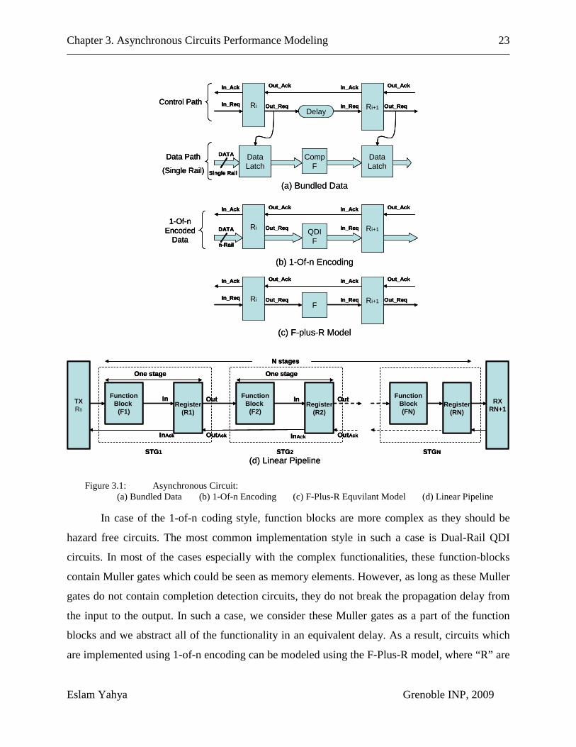
In case of the 1-of-n coding style, function blocks are more complex as they should be
hazard free circuits. The most common implementation style in such a case is Dual-Rail QDI
circuits. In most of the cases especially with the complex functionalities, these function-blocks
contain Muller gates which could be seen as memory elements. However, as long as these Muller
gates do not contain completion detection circuits, they do not break the propagation delay from
the input to the output. In such a case, we consider these Muller gates as a part of the function
blocks and we abstract all of the functionality in an equivalent delay. As a result, circuits which
are implemented using 1-of-n encoding can be modeled using the F-Plus-R model, where “R” are

Chapter 3. Asynchronous Circuits Performance Modeling 24
Eslam Yahya Grenoble INP, 2009
implementing the handshaking protocol with the corresponding transition delays, and “F” are
abstracting the hazard free function-blocks into an equivalent time delay.
In practice and for both implementation styles, function blocks can be easily analyzed by
standard timing analysis tools. Moreover, these function blocks are not depending on the
handshaking protocol implementation. For example, moving from WCHB to FDFB is not
affecting the function-block implementation. As a result, it is efficient to make the timing
analysis for the function blocks once and then abstract it as a time delay. After that we can insert
this function blocks into different circuits with different handshaking protocols.
The structural conventions in the F-plus-R model, Figure 3.1 (d), are that the pipeline is
composed of Stages “STG”, each stage is marked by an index (STG1, STG2, …. , STGN
3.2.2 Circuit Models for Linear Structures
). Each
stage is composed of a Register and any number of Function Blocks. TX and RX are modeling
the Input/Output characteristics of the environment. More details about modeling different
registers are explained in the next sub-sections.
In our method, the circuit model is based on Dependency Graphs [45], [43]. A
Dependency Graph is a time-marked directed-graph where the nodes of the graph correspond to
specific rising or falling transitions of circuit components, and the edges represent the
dependencies between signal transitions. The delay of each transition is represented by a value
assigned to the corresponding node in the graph.
Figure 3.2 (a) shows the circuit implementation of a Dual-Rail WCHB register, the circuit
is delimited by a dashed box. Due to the F-plus-R model, this circuit is to be abstracted to R
component; the interface outside the dashed box shows the F-plus-R abstraction of this circuit.
During the abstraction, if gates C1 and C2 have the same delays (say 60 ps), the register is
abstracted by a forward delay which is equal to 60 ps. Suppose C1 has a delay of 60 ps and C2
has a delay of 40 ps, the way that we calculate the forward delay is by multiplying probability of
going through C1 by its delay and the probability of going through C2 by its delay. In this way,
we can construct a statistical delay profile for the abstracted “R”. By means of this abstraction,

Chapter 3. Asynchronous Circuits Performance Modeling 25
Eslam Yahya Grenoble INP, 2009
bundled data, dual-rail and 1-of-8 registers end up with the same abstracted model with different
delay profiles.
TX
TX
F1 R1
F1 R1
A1
F2 R4
F2 R4
A4A1 A4
R2
R2
A2 A2
F3
F3
R3
R3
A3 A3
F4
F4
RX
RX
O_A O_A
R0 RegN+1
C2
C1 Out0
Out1
In0
In1
InAck
Reset
Reset OutAck
In_Req Out_Req
(a) F-plus-R abstraction for Dual-Rail WCHB Register
(c) Dependency Graph of Linear Pipeline based on WCHB Register
(b) Linear Pipeline
TXR0
FunctionBlock
(F1)Register
(R1)
FunctionBlock(FN)
Register(RN)
RXRN+1
One stage
InAck OutAck
FunctionBlock
(F2)Register
(R2)
N stages
One stage
In
InAck
Out
OutAck
In Out
STG1 STG2 STGN
TX
TX
F1 R1
F1 R1
A1
F2 R4
F2 R4
A4A1 A4
R2
R2
A2 A2
F3
F3
R3
R3
A3 A3
F4
F4
RX
RX
O_A O_A
R0 RegN+1TX
TX
F1 R1
F1 R1
A1
F2 R4
F2 R4
A4A1 A4
R2
R2
A2 A2
F3
F3
R3
R3
A3 A3
F4
F4
RX
RX
O_A O_A
R0 RegN+1TX
TX
F1 R1
F1 R1
A1
F2 R4
F2 R4
A4A1 A4
R2
R2
A2 A2
F3
F3
R3
R3
A3 A3
F4
F4
RX
RX
O_A O_A
R0 RegN+1
C2
C1 Out0
Out1
In0
In1
InAck
Reset
Reset OutAck
In_Req Out_Req
C2
C1 Out0
Out1
In0
In1
InAck
Reset
Reset OutAck
In_Req Out_Req
(a) F-plus-R abstraction for Dual-Rail WCHB Register
(c) Dependency Graph of Linear Pipeline based on WCHB Register
(b) Linear Pipeline
TXR0
FunctionBlock
(F1)Register
(R1)
FunctionBlock(FN)
Register(RN)
RXRN+1
One stage
InAck OutAck
FunctionBlock
(F2)Register
(R2)
N stages
One stage
In
InAck
Out
OutAck
In Out
STG1 STG2 STGN
TXR0
FunctionBlock
(F1)Register
(R1)
FunctionBlock(FN)
Register(RN)
RXRN+1
One stage
InAck OutAck
FunctionBlock
(F2)Register
(R2)
N stages
One stage
In
InAck
Out
OutAck
In Out
STG1 STG2 STGN
Figure 3.2: Dependency Graph of a linear-pipeline circuit which is based on WCHB protocol
Chapter 3. Asynchronous Circuits Performance Modeling 26
Eslam Yahya Grenoble INP, 2009
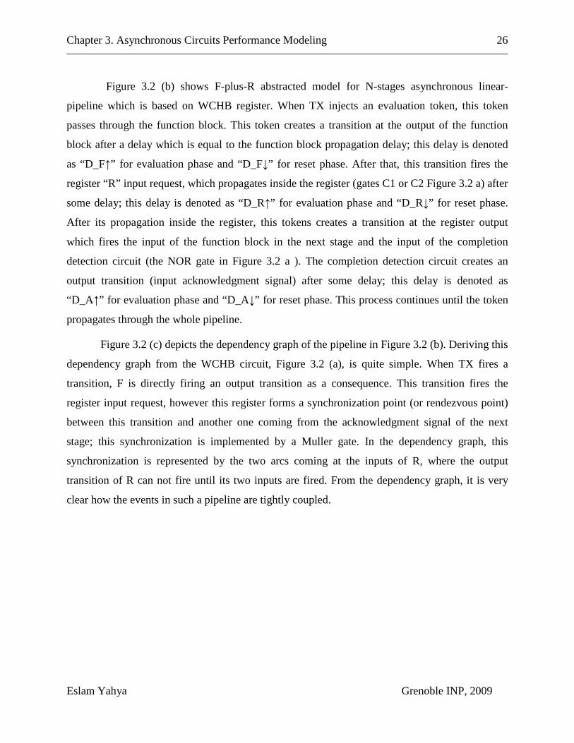
Figure 3.2 (b) shows F-plus-R abstracted model for N-stages asynchronous linear-
pipeline which is based on WCHB register. When TX injects an evaluation token, this token
passes through the function block. This token creates a transition at the output of the function
block after a delay which is equal to the function block propagation delay; this delay is denoted
as “D_F↑” for evaluation phase and “D_F↓” for reset phase. After that, this transition fires the
register “R” input request, which propagates inside the register (gates C1 or C2 Figure 3.2 a) after
some delay; this delay is denoted as “D_R↑” for evaluation phase and “D_R↓” for reset phase.
After its propagation inside the register, this tokens creates a transition at the register output
which fires the input of the function block in the next stage and the input of the completion
detection circuit (the NOR gate in Figure 3.2 a ). The completion detection circuit creates an
output transition (input acknowledgment signal) after some delay; this delay is denoted as
“D_A↑” for evaluation phase and “D_A↓” for reset phase. This process continues until the token
propagates through the whole pipeline.
Figure 3.2 (c) depicts the dependency graph of the pipeline in Figure 3.2 (b). Deriving this
dependency graph from the WCHB circuit, Figure 3.2 (a), is quite simple. When TX fires a
transition, F is directly firing an output transition as a consequence. This transition fires the
register input request, however this register forms a synchronization point (or rendezvous point)
between this transition and another one coming from the acknowledgment signal of the next
stage; this synchronization is implemented by a Muller gate. In the dependency graph, this
synchronization is represented by the two arcs coming at the inputs of R, where the output
transition of R can not fire until its two inputs are fired. From the dependency graph, it is very
clear how the events in such a pipeline are tightly coupled.

Chapter 3. Asynchronous Circuits Performance Modeling 27
Eslam Yahya Grenoble INP, 2009
+
C1Out0
+
C2Out1
In0
In1
OutAck
C3InAck
Reset
Reset
Set
+
C4
-
+
+
C1
+
C1Out0
+
C2
+
C2Out1
In0
In1
OutAck
C3InAck
Reset
Reset
Set
+
C4
-
+
(a) PCHB Schematic
OutAck
+
C1Out0
+
C2Out1
In0
In1
C3InAck
Reset
Reset
+
OutAck
+
C1
+
C1Out0
+
C2
+
C2Out1
In0
In1
C3InAck
Reset
Reset
+
(b) PCFB Schematic (c) FDFB Schematic
+
C3Out0
+
C4Out1
In0
In1
OutAck
InAck
Reset
Reset
C5
C1
C2
Reset
+
C3
+
C3Out0
+
C4
+
C4Out1
In0
In1
OutAck
InAck
Reset
Reset
C5
C1
C2
Reset
O_A
RegN+1F1 R1
F1 R1
A1
F2 R2
F2 R2
A2
F3 R3
F3 R3
A3
FB4 R4
FB4 R4
ACK4A1 A2 A3 A4
TX
TX
Reg0RX
RX
O_A O_A
RegN+1F1 R1
F1 R1
A1
F2 R2
F2 R2
A2
F3 R3
F3 R3
A3
FB4 R4
FB4 R4
ACK4A1 A2 A3 A4
TX
TX
Reg0RX
RX
O_A
F1 R1
F1 R1
F2 R2
F2 R2
A2
FB3 Reg3
FB3 Reg3
ACK3
F4 R4
F4 R4
A4Int1 Int2 Int3 Int4A1
A2 ACK3 A4Int1 Int2 Int3 Int4A1
TX
TX
Reg0RX
RX
O_A O_A
RegN+1F1 R1
F1 R1
F2 R2
F2 R2
A2
FB3 Reg3
FB3 Reg3
ACK3
F4 R4
F4 R4
A4Int1 Int2 Int3 Int4A1
A2 ACK3 A4Int1 Int2 Int3 Int4A1
TX
TX
Reg0RX
RX
O_A O_A
RegN+1
F1 R1
F1 R1
F2 R2
F2 R2
A2
F3 R3
F3 R3
A3
F4 R4
F4 R4
ACK4Int1 Int2 Int3 Int4A1
A2 A3 ACK4Int1 Int2 Int3 Int4A1
FInt1 FInt2 FInt3 FInt4
FInt1 FInt2 FInt3 FInt4
TX
TX
Reg0RX
RX
O_A O_A
RegN+1F1 R1
F1 R1
F2 R2
F2 R2
A2
F3 R3
F3 R3
A3
F4 R4
F4 R4
ACK4Int1 Int2 Int3 Int4A1
A2 A3 ACK4Int1 Int2 Int3 Int4A1
FInt1 FInt2 FInt3 FInt4
FInt1 FInt2 FInt3 FInt4
TX
TX
Reg0RX
RX
O_A O_A
RegN+1
(d) Dependency Graph of Linear Pipeline based on PCHB Register
(e) Dependency Graph of Linear Pipeline based on PCFB Register
(f) Dependency Graph of Linear Pipeline based on FDFB Register
Figure 3.3: Dependency Graphs of a linear-pipeline circuit which is based on PCHB, PCFB and FDFB

Chapter 3. Asynchronous Circuits Performance Modeling 28
Eslam Yahya Grenoble INP, 2009
Figure 3.3 (d, e and f) shows the dependency graphs of PCHB, PCFB and FDFB
protocols respectively. From the PCHB register schematic, Figure 3.3 (a), we can easily derive its
dependency graph. In the evaluation phase, PCHB is the same as WCHB. In the reset phase, we
can see that register Ri can generate a transition on its output independently of the reset transition
coming from the function block Fi
In addition to function-blocks and linear-registers, the above dependency graphs show
how to model the token producer (transmitter) “TX” and token consumer (receiver) “RX”. These
components are mandatory for modeling the environment interaction with the circuit.
; the Token Expectation Gain (Section 2.2.2). Regarding
PCFB, the internal state “Int”, the output of C4 in Figure 3.2 (b), makes the register able to
memorize a reset token in addition to the unacknowledged evaluation token. However, the
opposite order of the tokens is not possible, note the asymmetry in the dependency graph. The
FDFB dependency graph is completely symmetric which shows its regular capacity regardless
the order of the incoming tokens. The process of deriving the dependency graph from the circuit
is a systematic process. This formal representation is able to capture different asynchronous-
circuit styles.
3.2.2 Circuit Models for Nonlinear Structures
As discussed in Chapter 2, asynchronous nonlinear structures are classified into two
categories; Deterministic (or Choice Free) and non-deterministic (structures with choices). Most
of the previous works restricted their models to the deterministic nonlinear structures [26]. Few
of them slightly extended their work to cover limited classes on nondeterministic pipelines [20]
[51]. Most of these works relies on graph solutions of the Petri-net models of their circuits.
Solving Petri nets with choices is quite complex and is a time consuming problem. This explains
the restriction to either choice free circuit classes or limited circuit classes with choice. In this
PhD we propose a general and efficient solution for both nonlinear structures.
Deterministic-Nonlinear Structures: there are two nonlinear registers which are
deterministic, Forks “Fk” and Joins “J”. Figure 3.4 (a) shows the F-plus-R model of a Fork which
is connected to a circuit. Forks have a single input channel and multi output channels (from 2 to
n). When a token is injected to the input channel of the Fork, this token is duplicated n-times and
injected to all the Fork output channels; this is why some authors name Forks as “Duplicators”.

Chapter 3. Asynchronous Circuits Performance Modeling 29
Eslam Yahya Grenoble INP, 2009
The Dependency Graph, “DG”, of WCHB Fork is depicted in Figure 3.4 (b). Compared to
the dependency graph of a WCHB linear register (Figure 3.2 (c)), the Fork DG is the same except
that it is connected to multi outputs. Consequently, once the Fork produces a transition on its
output (Fk↑), this transition fires n-transitions (two in the graph Fx↑ and Fy↑). In addition, the
Fork is collecting the acknowledgment of its output branches. This is why Fk↑ has dependencies
on both Ax↑ and Ay↑. Despite that, the Fork DG is the same as a linear register DG. Deriving the
DGs of the other protocols is a straightforward process. We use the DG of a linear register and
duplicate its output dependencies n-times where “n” is the number of the Fork output branches.
Figures 3.5 (a, b and c) show the DG of PCHB, PCFB and FDFB Forks respectively.
Figures 3.6 (a and b) show the F-plus-R model and the DG of a WCHB Join. Joins have a
multi input channels, (from 2 to n), and single output channel. Joins collect n-input tokens and
produce one output token at the output channel. Similarly to Forks, DG of different Join
protocols can be derived from linear register DGs. Depending on the required protocol, we place
the proper linear register DG and duplicate its input dependencies n-times, where “n” is the
number of the Join input-channels. The DGs of PCHB, PCFB and FDFB Joins are depicted in
Figure 3.7 (a, b and c)

Chapter 3. Asynchronous Circuits Performance Modeling 30
Eslam Yahya Grenoble INP, 2009
(a) F-plus-R Model for a Fork Connected in a Circuit
(b) Dependency Graph for a WCHB Fork
Rz
Rz
F
F
Fk
Fk
A A
Fx
Fx
FY
FY
Rx
RY
Rx
RY
AX
AY
AX
AY
Rz
Rz
F
F
Fk
Fk
A A
Fx
Fx
FY
FY
Rx
RY
Rx
RY
AX
AY
AX
AY
FkFZRZ
A
FX RX
FY RY
AX
AY
LPZ
LPX
LPY
FkFZRZ
A
FX RX
FY RY
AX
AY
LPZ
LPX
LPY
Figure 3.4: Dependency Graph of WCHB Fork

Chapter 3. Asynchronous Circuits Performance Modeling 31
Eslam Yahya Grenoble INP, 2009
Rz
Rz
F
F
Fk
Fk
A A
Fx
Fx
FY
FY
Rx
RY
Rx
RY
AX
AY
AX
AY
Rz
Rz
F
F
Fk
Fk
A A
Fx
Fx
FY
FY
Rx
RY
Rx
RY
AX
AY
AX
AY
Rz
Rz
Fk
Fk
Fx
Fx
FY
FY
Rx
RY
Rx
RY
AX
AY
AX
AY
F
F
A Int
A Int
Rz
Rz
Fk
Fk
Fx
Fx
FY
FY
Rx
RY
Rx
RY
AX
AY
AX
AY
F
F
A Int
A Int
Rz
Rz
Fk
Fk
Fx
Fx
FY
FY
Rx
RY
Rx
RY
AX
AY
AX
AY
F
F
A Int
A Int
FInt
FIntRz
Rz
Fk
Fk
Fx
Fx
FY
FY
Rx
RY
Rx
RY
AX
AY
AX
AY
F
F
A Int
A Int
FInt
FInt
(a) Dependency Graph of PCHB Fork
(b) Dependency Graph of PCFB Fork
(c) Dependency Graph of FDFB Fork
Figure 3.5: Dependency Graph of PCHB, PCFB and FDFB Fork
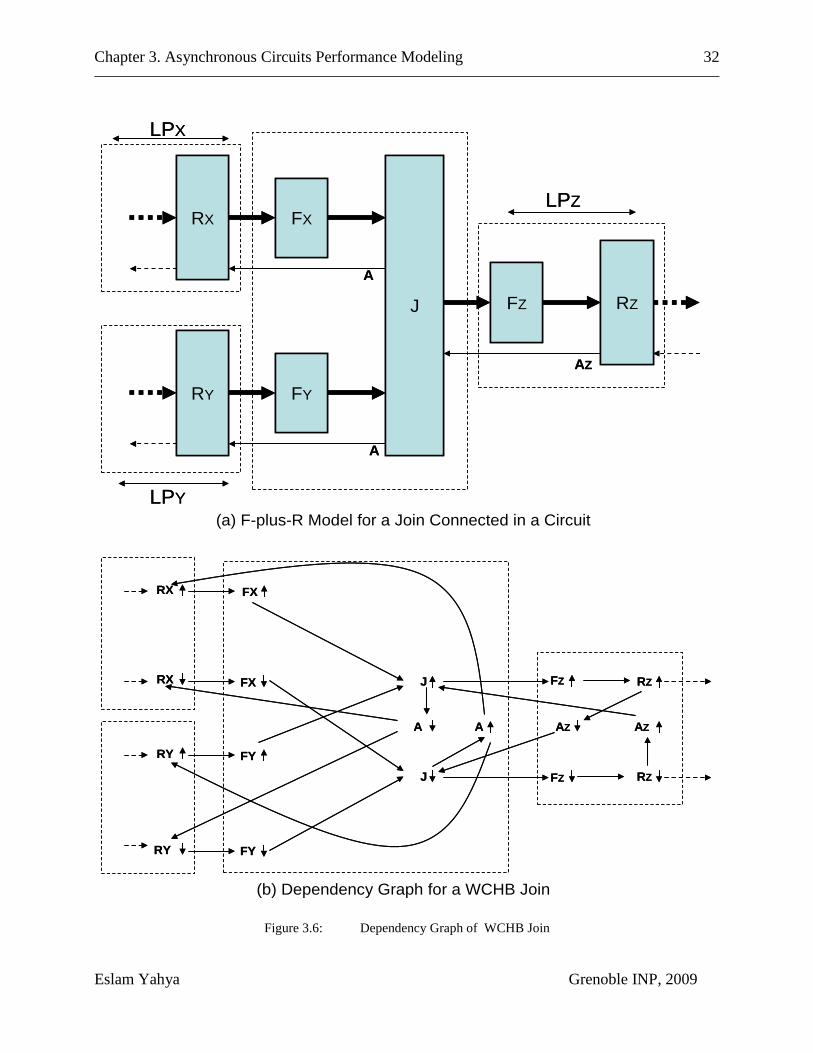
Chapter 3. Asynchronous Circuits Performance Modeling 32
Eslam Yahya Grenoble INP, 2009
(a) F-plus-R Model for a Join Connected in a Circuit
(b) Dependency Graph for a WCHB Join
RX
RX
RY
RY
FX
FY
FX
FY
J
J
FZ
FZ
A A
RZ
RZ
AZ AZ
RX
RX
RY
RY
FX
FY
FX
FY
J
J
FZ
FZ
A A
RZ
RZ
AZ AZ
J FZ RZ
AZ
FXRX
FYRY
A
A
LPZ
LPX
LPY
J FZ RZ
AZ
FXRX
FYRY
A
A
LPZ
LPX
LPY
Figure 3.6: Dependency Graph of WCHB Join
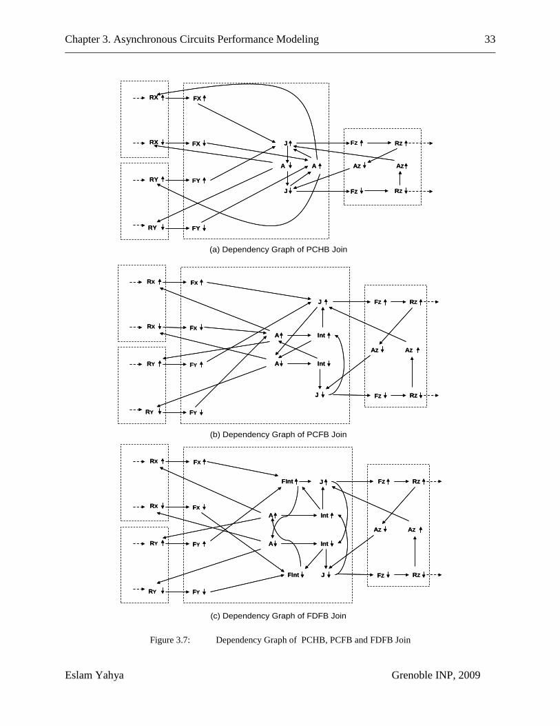
Chapter 3. Asynchronous Circuits Performance Modeling 33
Eslam Yahya Grenoble INP, 2009
(a) Dependency Graph of PCHB Join
(b) Dependency Graph of PCFB Join
(c) Dependency Graph of FDFB Join
RX
RX
RY
RY
FX
FY
FX
FY
J
J
A Int
A Int
FZ
FZ
RZ
RZ
AZ AZ
RX
RX
RY
RY
FX
FY
FX
FY
J
J
A Int
A Int
FZ
FZ
RZ
RZ
AZ AZ
RX
RX
RY
RY
FX
FY
FX
FY
FZ
FZ
RZ
RZ
AZ AZ
J
J
A Int
A Int
FInt
FInt
RX
RX
RY
RY
FX
FY
FX
FY
FZ
FZ
RZ
RZ
AZ AZ
J
J
A Int
A Int
FInt
FInt
RX
RX
RY
RY
FX
FY
FX
FY
J
J
FZ
FZ
A A
RZ
RZ
AZ AZ
RX
RX
RY
RY
FX
FY
FX
FY
J
J
FZ
FZ
A A
RZ
RZ
AZ AZ
Figure 3.7: Dependency Graph of PCHB, PCFB and FDFB Join

Chapter 3. Asynchronous Circuits Performance Modeling 34
Eslam Yahya Grenoble INP, 2009
Nondeterministic-Nonlinear Structures: Modeling asynchronous structures with choices
is always challenging. Petri nets are the modeling environment used to model asynchronous
systems in most of the literature. Solving Petri nets with choices is quite complex especially
when graph analysis methods are used. As previous works, we are using conditional Petri nets to
model structures with choices. However, our solving methodology is efficient enough to get rid
of the complexity of solving such models. That is discussed in more details in the next chapters.
Normally, Dependency graphs are choice free graphs. However, they are a subset of Petri
nets so we can extend them to implement systems with choices. Figure 3.8 (a) shows the F-plus-
R model for a split structure “S”. Splits have a single input channel, “n” output-channels and a
control channel. When a token is injected to the input of a Split, this token is passed to a single
output channel which is determined by the control (selection) value. This functionality is
identical to the standard DEMUX functionality. The control input is modeled as an input channel
with a function block called “Cnt”. This function block expresses the delay characteristics of the
control channel. The register “Rc” is modeling the handshaking between the control-signal
generator and the Split. From the behavior point of view, there are dependencies between the
Split and all of its output channels. Unlike Forks, Split output has a dependency with a single
output channel per each data transfer. The selection of this output is determined by the value of
the control input. As a result, the dependency graph of the split, depicted in Figure 3.8 (b), is
similar to the dependency graph of a Fork except that all the dependencies between the Split
output and the output channels are conditioned by the value of the control input. In Figure 3.8,
the split has two output channels, x-channel and y-channel. Consequently, the control input has
either a value of “C0” (to select the x-channel) or a value of “C1” (to select the y-channel). In the
DG, all dependencies between S↑↓ and (Fx↑↓/Fy↑↓ , Ax↑↓/Ay↑↓) are conditioned by C0/C1.
Similarly, F-plus-R model and dependency graph of a Merge “M” are shown in Figure 3.9
(a and b) respectively. This time the control input determines which input channel is injected to
the output channel. This is similar to MUX functionality. The DGs of PCHB, PCFB and FDFB
Split/Merges can be systematically derived in a similar way as the WCHB ones.

Chapter 3. Asynchronous Circuits Performance Modeling 35
Eslam Yahya Grenoble INP, 2009
Rz
Rz
F
F
S
S
A A
Fx
Fx
FY
FY
Rx
RY
Rx
RY
AX
AY
AX
AY
C1
C1C0
C1
C0
C0
C0
C1
Rz
Rz
F
F
S
S
A A
Fx
Fx
FY
FY
Rx
RY
Rx
RY
AX
AY
AX
AY
C1
C1C0
C1
C0
C0
C0
C1
(a) F-plus-R Model for a Split Connected in a Circuit
(b) Dependency Graph for a WCHB Split
SFZRZ
A
FX RX
FY RY
AX
AY
RC
Cnt
AC
SFZRZ
A
FX RX
FY RY
AX
AY
RC
Cnt
AC
Figure 3.8: Dependency Graph of WCHB Split

Chapter 3. Asynchronous Circuits Performance Modeling 36
Eslam Yahya Grenoble INP, 2009
RX
RX
RY
RY
FX
FY
FX
FY
J
J
FZ
FZ
A A
RZ
RZ
AZ AZC0
C0
C0
C0
C1
C1
C1
C1
RX
RX
RY
RY
FX
FY
FX
FY
J
J
FZ
FZ
A A
RZ
RZ
AZ AZC0
C0
C0
C0
C1
C1
C1
C1
(a) F-plus-R Model for a Merge Connected in a Circuit
(b) Dependency Graph for a WCHB Merge
M FZ RZ
AZ
FXRX
FYRY
A
A
RC
Cnt
AC
M FZ RZ
AZ
FXRX
FYRY
A
A
RC
Cnt
AC
Figure 3.9: Dependency Graph of WCHB Merge
Chapter 3. Asynchronous Circuits Performance Modeling 37
Eslam Yahya Grenoble INP, 2009
3.3 Delay Model
No doubt that Static Timing Analysis “STA” is not a sufficient technique for analyzing
circuit performance especially with the recent technologies. Particularly with asynchronous
systems performance analysis, considering time variability is mandatory. Asynchronous circuits
are self timed which makes their performance affected much by variability. Same asynchronous
component could have different response times as many as the number of delays it has. That
makes asynchronous circuit having variable performance depending on the instantaneous delay
value of each component. Considering variability while analyzing asynchronous circuit is
mandatory not only for timing analysis, but also for the Electromagnetic Interference “EMI” and
reliability against process variability. Most of previous works consider average delays or static
time delays for the circuit components. This is not an accurate assumption as the main benefit of
asynchronous circuits, from the performance point of view, is their ability to compute in average
time instead of worst case which reduces the pessimism.
In this section, we briefly introduce some important concepts about delay variability and
its sources. After that, some investigations about the delay Probability Density Functions “PDF”
used in ST-Microelectronics technologies are done. Afterward, our delay model is introduced.
The main goals we take into consideration while choosing our delay model are as follows:
1. Generality: we need a model which is able to represent different delay types (average,
deterministic and statistical).
2. Adaptability: this is one of the most important goals as we want a model which adapts its
computation complexity to the delay characteristics. That means the model should be able to
represent complex statistical PDFs and become simple when static delays are used.
3. Simplicity: to reduce the computation needs as much as possible for obtaining an efficient
method this is able to analyze complex circuits in a reasonable time.
Parameters chosen by the designer are perturbed from their nominal values. Sources of
variation can be broadly classified into two classes [40], Process Variation and Environmental
Variation.
Process Variation: due to perturbations in the fabrication process (W, L, …).

Chapter 3. Asynchronous Circuits Performance Modeling 38
Eslam Yahya Grenoble INP, 2009
1. Inter-die variation: variation from die to die, and affect all the devices on the same chip in the
same way.
2. Intra-die variation: variability within a single die. It may affect devices on the same chip in a
different way.
Simulating the design at different corners solved the Inter-die variation for many years. However,
the intra-die variation could not be managed in the same way.
Environmental variation: due to the change in the operating conditions of the circuit.
(Supply voltage, Temp, radiation, ….)
A third source of variation can be identified; it is the Data Dependency. In this case we
take into account the variation in the circuit response depending on the value of the processed
data. One good example is the time response of an adder. These sources introduce variations
which are different in their nature. One can identify two main classes of the variation nature.
Random Variations: depicts random behavior that can be characterized in terms of a
distribution. This distribution may either be explicit (large number of samples provided by the
fab-house) or implicit (PDF).
Systematic Variation: show predictable variation-trends across a chip.
Random variations in some process or environmental parameters (as supply voltage and
temperature) often show some degree of local Spatial-Correlation, whereby variations in one
transistor in a chip are similar in nature to those in spatially-neighboring transistors. However,
they may significantly differ from transistors those are spatially far away.
Statistical Static Timing Analysis (SSTA): It is an extension of traditional STA
techniques to move beyond their deterministic nature. SSTA treats delays not as fixed numbers,
but as Probability Density Functions (PDFs).
At this level, we are in need to know what kinds of PDFs are used in different
technologies to model the delay variability. We did our investigation targeting 65nm and 45nm
ST-Microelectronics CMOS technologies since our TAL library is based on them. We used
simulation based methods for extracting the used PDFs. Various components of the TAL library

Chapter 3. Asynchronous Circuits Performance Modeling 39
Eslam Yahya Grenoble INP, 2009
are tested by composing them in circuits and doing MontCarlo simulation for their propagation
delays. Figure 3.10 shows an example of a test circuit for investigating the PDFs of an inverter.
Figure 3.10: Example of Test Circuit for investigating the used PDFs
In all the circuits, results always showed a Gaussian distribution for the propagation
delays in both cases of inter-die and intra-die variation and the composition of both. These results
are consistent with the results presented in [32] [27] which are extracted by simulation and
measuring of different silicon runs. Since the Gaussian PDF is widely used to model different
process variation, we did some investigation about the mathematical properties of this
distribution. However, we insisted while designing our delay model on generality (ability of
representing other PDF).

Chapter 3. Asynchronous Circuits Performance Modeling 40
Eslam Yahya Grenoble INP, 2009
Gaussian distribution is an important family of continuous probability distributions. Each
member of the family may be defined by two parameters, the mean ("average", μ) and variance
(standard deviation squared) σ2
Standard Deviation σ: In probability and statistics, the standard deviation is a measure of
the dispersion of a set of values.
, respectively.
Variance σ2
To indicate that a real-valued random variable X is normally distributed with mean μ and
variance σ² ≥ 0, we write: X ≈ N (μ , σ
: The variance of a random variable, probability distribution, or sample is one
measure of statistical dispersion, averaging the squared distance of its possible values from the
expected value (mean).
2
Standard deviation and confidence intervals: there is very important rule for Gaussian
distributions; it is called the Empirical Rule (also known as 68-95-99.7 rule, or three-sigma
rule). Figure 3.11 shows this rule.
).
Figure 3.11: Empirical Rule
The empirical rule tells us that if the data follows a normal distribution approximately
68% of the data values can be expected to lie within a one standard deviation interval around the
mean. Approximately 95% of the data values can be expected to lie within a two standard
deviation interval around the mean. Virtually all (approximately 99.7%) of the data values can be
expected to lie within a three standard deviation interval around the mean. To be able to claim
that a data sample is normally distributed we have to insure that the samples are following the

Chapter 3. Asynchronous Circuits Performance Modeling 41
Eslam Yahya Grenoble INP, 2009
Empirical rule. This, for sure, implies some conditions on the minimum number of values
representing this data.
One important property we recall here is the mathematical composition of two Gaussian
PDFs. If and are independent normal random variables,
then their sum is normally distributed with:
(3.1)
One other way to obtain the sum is to compute the convolution of the two density
functions.
3.3.1 Modeling variability in circuit components
Delay variability in a circuit component can be modeled in two ways:
1. By using a PDF representing the delay variability. This PDF is sampled and used when
composing this component with another one. Normally the delays of the circuit component
will be added to each others in each logic stage (Stage is composed of combinational logic
and registers). Adding delays represented by PDFs is done by convolving them.
Advantages: With relatively few numbers of samples we can represent the PDF,
especially if it is regular PDF as Gaussian distribution.
Disadvantages: It is restricted to regular delay distributions. Moreover, the algorithm of
the convolution is complex from the point of view of computational needs. The convolution of
two-sampled PDF will result another PDF but represented by more samples. In other words,
convolution results in increasing number of samples. This property forces any simulator using
convolution to watch the size of results and reduce the number of samples to avoid size-
explosions especially in large circuits [32]. Reducing number of samples is not a trivial operation
(from processing time point of view).
2. By using a sample which is following the delay PDF; we call this sample “Delay Vector”.
Each value of this vector represents a possible delay value. The overall distribution of the
delay-values is representing the component delay-PDF.

Chapter 3. Asynchronous Circuits Performance Modeling 42
Eslam Yahya Grenoble INP, 2009
Advantages: Generality; this way of representation enables representing regular PDFs as
well as irregular variability distributions. In addition of that, it needs simple operation to solve
the composition of two components; it is just an addition. In this case, adding two delay vectors
to each others producing the same number of samples. In other words, using this representation
gives number of samples at the output, which is equivalent to the number of samples in the input
(no sample increasing).
Disadvantages: First, we must start with relatively high number of samples to insure a
reasonable accuracy in representing the PDF.
3.3.2 Delay Token Vector
Delays in our model are found in Function Blocks “F” and Registers “R”. Time
characteristics of the environment are modeled by TX and RX. Each circuit component is
assigned a Delay Token Vector “DTV”. The DTV consists in a list of delay pairs [Di,j↑, Di,j
D
↓].
Whereas:
i,j
D
↑: the delay that component “i” needs to complete the evaluation of Token “j”.
i,j
i: the component index inside the circuit.
↓: the delay that component “i” needs to complete the reset of Token “j”.
j: the input-token index.
Every component in the circuit has its own DTV which specifies the component delay
characteristics. This model can simply represent static delays as well as time variable delays. If a
component is assigned average delay, the DTV of this component consists of a single pair
holding the evaluation and reset delays. In case of deterministic time variable delays, the DTV is
an ordered list of pairs providing a delay value each time the component is executed. If the
component has probabilistic delays then the DTV is filled with delay pairs which are following
the PDF of the delays. If the delay variation does not fit to a regular PDF and they are large
number of samples provided from fabrication line measurements, this case can be easily
implemented by the DTV where the samples are the vector components. The last case is

Chapter 3. Asynchronous Circuits Performance Modeling 43
Eslam Yahya Grenoble INP, 2009
practically very common especially when composed process and environmental variation-sources
are taken into consideration. To the best of our knowledge, none of the previous works has the
ability to support such situation.
As discussed earlier, we are targeting a General and Adaptable delay model. The DTV is
a general delay model hence it is able to capture all the possible delay natures especially those
having irregular variability distributions. In addition of that, the length of the DTV is proportional
to the complexity of the delay nature. This property makes our delay model completely
adaptable. If we insure that the complexity of the methodology is proportional to the DTV length
then the adaptability to the delay nature is guaranteed. This point is discussed in more details in
the next chapter.
Variability Characteristics
DTVGenerator
Extracted Delays by Standard Tools
DTVs for Circuit Components
Variability Characteristics
DTVGenerator
Extracted Delays by Standard Tools
DTVs for Circuit Components
Figure 3.12: Delay Token Vector “DTV” Generator
Figure 3.1 shows the block diagram of the DTV generator. First, delay characteristics for
each circuit component are extracted by standard timing analysis tools. After that and by using
library specifying the variability characteristics for the technology, a module called “DTV
Generator” generates the DTVs for the circuit components. The implementation of this module is
discussed in details in the chapter devoted to tools implementation.

Chapter 3. Asynchronous Circuits Performance Modeling 44
Eslam Yahya Grenoble INP, 2009
As discussed in sub-section 3.3.1, there are two ways to model variability in the circuit
component, by using PDFs or by using sampled vectors. Our delay model falls in the second
category. This is the key reason which gave our model its generality and adaptability. However,
the possible disadvantage of this way of modeling is the need for quite large number of samples
for reaching a reasonable accuracy. For investigating this point, we made many test circuit in 65
nm and 45 nm ST-Microelectronics technology. In these circuits we computed the results of
cascading components in one circuit by using two methods:
1. Using Montecarlo simulations in the Cadence Analog Design Flow.
2. Using our Simulator which is based on the DTV model.
After that we compare the results by the exact delay PDF that is calculated
mathematically using Equation 3.1. The goal of this study is to end up with a figure about the
required DTV length to achieve a reasonable accuracy. Moreover, we should have an idea about
the performance of our delay model compared to the performance of the Montecarlo simulator.
One example for the test circuits is shown in Figure 3.10. This circuit is composed of
chains of inverters which are connected in series. By using the Cadence Montcarlo flow, the
delay-PDF of each inverter in the two branches is simulated. All inverters show Gaussian
distributions for their delays. This circuit is a simple combinational circuit, which means that
delays of the inverters are added to each others to determine the delay of the circuit. Since these
delays are Gaussian PDFs, there summation should follow Equation 3.1. By applying this
equation to calculate the total circuit delay, the delay is determined by the following relation:
µTotal↑ = (k x µInv↑) + (k x µInv↓) + µMul
σ
↑
2Total↑ = (k x σ2
Inv↑) + (k x σ2Inv↓) + σ2
Mul
↑ (3.2)
Where:
µTotal
µ
↑: is the mean of the total circuit-delay in the raising phase.
Inv
µ
↑: is the mean of the Inverter delay in the raising phase.
Inv↓: is the mean of the Inverter delay in the falling phase.

Chapter 3. Asynchronous Circuits Performance Modeling 45
Eslam Yahya Grenoble INP, 2009
µMul
σ
↑: is the mean of the Muller gate delay in the raising phase.
2Total
σ
↑: is the variance of the total circuit-delay in the raising phase.
2Inv
σ
↑: is the variance of the Inverter delay in the raising phase.
2Inv
σ
↓: is the variance of the Inverter delay in the falling phase.
2Mul
2k: is the number of Inverter in series.
↑: is the variance of the Muller gate delay in the raising phase
This test circuit is simulated while considering the intra-die variation (named in Cadence
as “Mismatch”). After that, the same circuit is simulated while considering the inter-die variation
(named in Cadence as “Process”). Table 3.1 shows the comparison between the results obtained
from Montecarlo simulation, our DTV model and the exact delay distribution calculated by
Equation 3.2. A snapshot of the Montecarlo simulation done by Cadence is shown in Figure
3.13.
TABLE 3.1: COMPARISON BETWEEN MONTECARLO, DTV MODEL AND EXACT PDF (TIME VALUES IN PS)
Inv Mul Eq 3.2 Montcarlo DTV 10 102 103 104 103 104 105
µ↑ 6
9.86 44.4 459.6 0.39% 0.3% 0.23% 0.03% 0.05% 0.016% 0.018% µ↓ 10.9 47.2 462.4 0.32% 0.27% 0.21% 0.03% 0.06% 0.010% 0.009% σ↑ 0.47 2.81 3.89 27.7% 20% 15.2% 3.9 % 0.16% 0.06 % 0.02 % σ↓ 0.37 2.30 3.78 26.9% 19.3% 14.6% 3.5% 0.16% 0.06 % 0.019%
Second and third columns in Table 3.1 show the delays extracted from a post layout
simulation for the Inverter and the Muller gate. Fourth column shows the total delay for the
circuit shown in Figure 3.10 calculated using Equation 3.2 (where k=20). For readability of the
error, values of standard deviation “σ” are shown in the table. Fifth and sixth columns show the
error percentages of the same values extracted by Montecarlo simulation and by our DTV Model
respectively. From the table, it is clear that both models are following the mathematical rules
while computing the Mean by an error which is less than 1%. However, Montcarlo is giving high
error percentage in computing the standard deviation. The best we can have using 104 iterations
is an error of 15% which is taking very long simulation time (about 80 hours of CPU time). On

Chapter 3. Asynchronous Circuits Performance Modeling 46
Eslam Yahya Grenoble INP, 2009
the contrary, our DTV model could reach an error of 0.16% by using 104 samples. This
simulation is taking a fraction of a second to calculate the results. That gives significant
enhancement in terms of accuracy and simulation time for our model. We can conclude from
these results, that we can safely use our DTV model with 104 or 105 and we guarantee an error
percentage which is less that 1%. Moreover, using this number of samples is also mandatory, for
both methods (Montacarlo and DTV), to be sure that we respect the imperial rule.
Figure 3.13: Montcarlo Simulation for Inverter Circit
3.4 Analytical Model
Previous sections introduce how to model the circuit structure and how to model the
delays in the components. As discussed earlier, there are three main methods for analyzing the
performance, by using graph based methods, by using closed form equations or by using iterative

Chapter 3. Asynchronous Circuits Performance Modeling 47
Eslam Yahya Grenoble INP, 2009
simulations. Our analysis method is a mixture between closed form equations and the iterative
simulations. The idea is to derive a closed form equation which calculates the absolute time of the
output events in terms of the absolute time input events and the circuit components delays. This
closed form equation is solved for a single output event, equivalently single input token.
Afterwards, these closed form equations are iteratively solved the absolute time for the set of
output events which are corresponding to the set of input tokens.
In previous works, the absence of the clock is considered as the absence of any barrier
which is partitioning the circuit. As a result, the circuit is modeled in a marked graph and then
this graph is solved as a single problem either by Markov process as in [35] or by using iterative
simulation for the graph as in [51]. Both methods are suffering huge processing time and
possibility of state explosion. In the contrary, our method considers asynchronous registers as
barriers which are partitioning asynchronous circuit into separate islands. As shown in Figure
3.1 (d), the presence of each register is defining a stage. The interaction between each stage and
its neighbors is defined by the register handshaking protocol. If we can model this protocol, we
are able to solve the circuit as many simple problems instead of a single huge problem.
3.4.1 Analytical Models for Linear Registers
In this subsection, the analytical models of the asynchronous linear-registers are derived.
As an example, we derived the analytical models of the WCHB, PCHB, PCFB and FDFB
handshaking protocols. However, the methodology can be applied to any other handshaking
protocol provided that the circuit model of this protocol is available.
TX
TX
F1 R1
F1 R1
A1
F2 R4
F2 R4
A4A1 A4
R2
R2
A2 A2
F3
F3
R3
R3
A3 A3
F4
F4
RX
RX
O_A O_A
R0 RegN+1TX
TX
F1 R1
F1 R1
A1
F2 R4
F2 R4
A4A1 A4
R2
R2
A2 A2
F3
F3
R3
R3
A3 A3
F4
F4
RX
RX
O_A O_A
R0 RegN+1TX
TX
F1 R1
F1 R1
A1
F2 R4
F2 R4
A4A1 A4
R2
R2
A2 A2
F3
F3
R3
R3
A3 A3
F4
F4
RX
RX
O_A O_A
R0 RegN+1TX
TX
F1 R1
F1 R1
A1
F2 R4
F2 R4
A4A1 A4
R2
R2
A2 A2
F3
F3
R3
R3
A3 A3
F4
F4
RX
RX
O_A O_A
R0 RegN+1
Figure 3.14: Deriving Analytical-Model for WCHB Linear Registers

Chapter 3. Asynchronous Circuits Performance Modeling 48
Eslam Yahya Grenoble INP, 2009
Time Token Vectors “TTV” : As discussed earlier, the objectives of the analytical model
is calculating the absolute time of the output events in terms of the absolute time input events and
the circuit components delays. The Absolute Time of an Event “is the time difference between
time zero and the occurrence of the event”; where Time Zero “is the time of a reference event
(usually the injection of the first token into the system)”. For each register output, there is a
vector which is holding the absolute times of this output events which are corresponding to the
input tokens. We call this vector as Time Token Vector “TTV”.
Figure 3.14 shows the circuit model of a pipeline which is based on WCHB registers.
Suppose that we want to derive the analytical equation which is calculating the TTV of register
“R3”. R3 has four output events, R3↑, R3↓, A3↑ and A3↓. Let’s start with R3
1. The absolute time of “R
↑ (the solid arcs), the
absolute time of this event is the maximum between:
2↑” (previous stage request “Evaluation”) plus the delay of “F3
2. The absolute time of “A
↑”
(current stage Function Block propagation delay “Evaluation”).
4
Analytically, this is written as follows:
↑” (next stage acknowledgment corresponding to the Reset part of
previous Data).
T_R3,j↑ = Max [ T_R2,j↑ + D_F3,j↑ ; T_A4,j-1↑ ] + D_R3,j
In the same way, the analytical equation for “R
↑
3
1. The absolute time of “R
↓” can be derived following the dashed
arcs, it is the maximum between:
2↓” (previous stage request “Reset”) plus the delay of “F3
2. The absolute time of “A
↓” (current
stage Function Block propagation delay “Reset”).
4
T_R
↓” (next stage acknowledgment corresponding to the Evaluation part
of current Data).
3,j↓ = Max [ T_R2,j↓ + D_F3,j↓ ; T_A4,j↓ ] + D_R3,j
In the same way, the equations of A
↓
3↑ and A3↓ can be derived. By generalizing the
equations, we have the following:

Chapter 3. Asynchronous Circuits Performance Modeling 49
Eslam Yahya Grenoble INP, 2009
T_Ri,j↑ = Max [ T_Ri-1,j↑ + D_Fi,j↑ ; T_Ai+1,j-1↑ ] + D_Ri,j
T_R
↑
i,j↓ = Max [ T_Ri-1,j↓ + D_Fi,j↓ ; T_Ai+1,j↓ ] + D_Ri,j
↓
T_Ai,j↓ = T_Ri,j↑ + D_A i,j
T_A
↓
i,j↑ = T_Ri,j↓ + D_A i,j
↑
(3.3.a)
(3.3.b)
Where:
i: is the stage index inside the circuit.
j: is the Data index.
T_Ri,j
T_R
↑: absolute time of the output event in register “i” corresponding to Evaluation phase of
Data “j”.
i,j
D_R
↓: absolute time of the output event in register “i” corresponding to Reset phase of Data “j”.
i,j
D_R
↑: propagation delay of register “i” corresponding to Evaluation phase of Data “j”.
i,j
D_F
↓: propagation delay of register “i” corresponding to Reset phase of Data “j”.
i,j
D_F
↑: propagation delay of Function Block “i” corresponding to Evaluation phase of Data “j”.
i,j
T_A
↓: propagation delay of Function Block “i” corresponding to Reset phase of Data “j”.
i,j
T_A
↓: absolute time of the acknowledgment event in register “i” corresponding to Evaluation
phase of Data “j”.
i,j
D_A
↑: absolute time of the acknowledgment event in register “i” corresponding to Reset phase
of Data “j”.
i,j
D_A
↓: propagation delay of register “i” acknowledgment corresponding to Evaluation phase of
Data “j”.
i,j↑: propagation delay of register “i” acknowledgment corresponding to Reset phase of Data
“j”.

Chapter 3. Asynchronous Circuits Performance Modeling 50
Eslam Yahya Grenoble INP, 2009
For readability of the equations we omit the propagation delay of the register “forward
propagation delay” and of the register-acknowledgment “reverse propagation delay”. This is done
just for readability; however, the propagation delays “Forward/Reverse” are included in the
implementation. After omitting these terms Equation 3.3 becomes:
WCHB :
T_Ri,j↑ = Max [ T_Ri-1,j↑ + D_Fi,j↑ ; T_Ai+1,j-1
T_R
↑ ]
i,j↓ = Max [ T_Ri-1,j↓ + D_Fi,j↓ ; T_Ai+1,j
↓ ]
T_Ai,j↓ = T_Ri,j
T_A
↑
i,j↑ = T_Ri,j
↓
(3.4.a)
(3.4.b)
In the same manner, the analytical models of PCHB, PCFB and FDFB registers can be
systematically derived from the corresponding circuit models appearing in Figure 3.3 (d, e, f)
respectively. After using the properties of the “Max” operation, the simplified equations of these
analytical models appear in Equations 3.5, 3.6 and 3.7.
PCHB:
T_Ri,j↑ = Max [ T_Ri-1,j↑ + D_Fi,j↑ ; T_Ai+1,j-1
T_R
↑ ]
i,j↓ = Max [T_Ai,j↓ ; T_Ai+1,j
↓ ]
T_Ai,j↓ = T_Ri,j
T_A
↑
i,j↑ = Max [ T_Ri-1,j↓ + D_Fi,j↓ ; T_Ri,j
↓]
(3.5.a)
(3.5.b)
PCFB :
T_Ri,j↑ = Max [ T_Ri-1,j↑ + D_Fi,j↑ ; T_Ai+1,j-1
↑ ] (3.6.a)

Chapter 3. Asynchronous Circuits Performance Modeling 51
Eslam Yahya Grenoble INP, 2009
T_Ri,j↓ = Max [T_Ai,j↓ ; T_Ai+1,j
↓ ]
T_Ai,j↓ = T_Ri,j
T_A
↑
i,j↑ = T_Ri-1,j↓ + D_Fi,j
↓
(3.6.b)
FDFB :
T_Ri,j↑ = Max [ T_Ri-1,j↑ + D_Fi,j↑ ; T_Ai+1,j-1
T_R
↑ ]
i,j↓ = Max [T_Ai,j↓ ; T_Ai+1,j
↓ ]
T_Ai,j↓ = Max [ T_Ri-1,j↑ + D_Fi,j↑ ; T_Ri,j-1
T_A
↓]
i,j↑ = Max [ T_Ri-1,j↓ + D_Fi,j↓ ; T_Ri,j
↑]
(3.7.a)
(3.7.b)
The handshaking protocol properties discussed in Chapter 2 can be seen clearly in the
analytical models. For example, by comparing the evaluation phase by and reset phase in
Equation 3.4, 3.5, 3.6 and 3.7, one can see that PCHB, PCFB and FDFB registers generates the
output reset event “T_Ri,j↓” once the acknowledgment corresponding to the evaluation token is
received from the next stage register “T_Ai+1,j
Same derivation rules can be systematically applied to the dependency graphs of Forks,
Joins, Splits and Merges.
↓”.
3.4.2 Analytical Models for Forks
The dependency graphs of the WCHB, PCHB, PCFB and FDFB Forks appear in Figures
3.4 and 3.5. The corresponding analytical models appear in Equations 3.8, 3.9, 3.10 and 3.11
respectively.

Chapter 3. Asynchronous Circuits Performance Modeling 52
Eslam Yahya Grenoble INP, 2009
WCHB :
T_Fki,j↑ = Max [ T_Ri-1,j↑ + D_Fi,j↑ ; T_AX,j-1↑ ; T_AY,j-1
T_Fk
↑]
i,j↓ = Max [ T_Ri-1,j↓ + D_Fi,j↓ ; T_AX,j↓ ; T_AY,j
↓]
T_Ai,j↓ = T_Fki,j
T_A
↑
i,j↑ = T_Fki,j
↓
(3.8.a)
(3.8.b)
PCHB:
T_Fki,j↑ = Max [ T_Ri-1,j↑ + D_Fi,j↑ ; T_AX,j-1↑ ; T_AY,j-1
T_Fk
↑]
i,j↓ = Max [T_Ai,j↓ ; T_AX,j↓ ; T_AY,j
↓]
T_Ai,j↓ = T_Fki,j
T_A
↑
i,j↑ = Max [ T_Ri-1,j↓ + D_Fi,j↓ ; T_Fki,j
↓]
(3.9.a)
(3.9.b)
PCFB :
T_Fki,j↑ = Max [ T_Ri-1,j↑ + D_Fi,j↑ ; T_AX,j-1↑ ; T_AY,j-1
T_Fk
↑]
i,j↓ = Max [T_Ai,j↓ T_AX,j↓ ; T_AY,j
↓]
T_Ai,j↓ = T_Fki,j
T_A
↑
i,j↑ = T_Ri-1,j↓ + D_Fi,j
↓
(3.10.a)
(3.10.b)
FDFB :
T_Fki,j↑ = Max [ T_Ri-1,j↑ + D_Fi,j↑ ; T_AX,j-1↑ ; T_AY,j-1
↑] (3.11.a)

Chapter 3. Asynchronous Circuits Performance Modeling 53
Eslam Yahya Grenoble INP, 2009
T_Fki,j↓ = Max [T_Ai,j↓ T_AX,j↓ ; T_AY,j
↓]
T_Ai,j↓ = Max [ T_Ri-1,j↑ + D_Fi,j↑ ; T_Fki,j-1
T_A
↓]
i,j↑ = Max [ T_Ri-1,j↓ + D_Fi,j↓ ; T_Fki,j
↑]
²
(3.11.b)
3.4.3 Analytical Models for Joins
The dependency graphs of the WCHB, PCHB, PCFB and FDFB Joins appear in Figures
3.6 and 3.7. The corresponding analytical models appear in Equations 3.12, 3.13, 3.14 and 3.15
respectively.
WCHB :
T_Ji,j↑ = Max [ T_RX,j↑ + D_FX,j↑ ; T_RY,j↑ + D_FY,j↑ ; T_AZ,j-1
T_J
↑ ]
i,j↓ = Max [ T_RX,j↓ + D_FX,j↓ ; T_RY,j↓ + D_FY,j↓ ; T_AZ,j
↓ ]
T_Ai,j↓ = T_Ji,j
T_A
↑
i,j↑ = T_Ji,j
↓
(3.12.a)
(3.12.b)
PCHB:
T_Ji,j↑ = Max [ T_RX,j↑ + D_FX,j↑ ; T_RY,j↑ + D_FY,j↑ ; T_AZ,j-1
T_J
↑ ]
i,j↓ = Max [T_Ai,j↓ ; T_AZ,j
↓ ]
T_Ai,j↓ = T_Ji,j
T_A
↑
i,j↑ = Max [ T_RX,j↓ + D_FX,j↓ ; T_RY,j↓ + D_FY,j↓ ; T_Ji,j
↓]
(3.13.a)
(3.13.b)

Chapter 3. Asynchronous Circuits Performance Modeling 54
Eslam Yahya Grenoble INP, 2009
PCFB :
T_Ji,j↑ = Max [ T_RX,j↑ + D_FX,j↑ ; T_RY,j↑ + D_FY,j↑ ; T_AZ,j-1
T_J
↑ ]
i,j↓ = Max [T_Ai,j↓ ; T_AZ,j
↓ ]
T_Ai,j↓ = T_Ji,j
T_A
↑
i,j↑ = Max [ T_RX,j↓ + D_FX,j↓ ; T_RY,j↓ + D_FY,j
↓ ]
(3.14.a)
(3.14.b)
FDFB :
T_Ji,j↑ = Max [ T_RX,j↑ + D_FX,j↑ ; T_RY,j↑ + D_FY,j↑ ; T_AZ,j-1
T_J
↑ ]
i,j↓ = Max [T_Ai,j↓ ; T_AZ,j
↓ ]
T_Ai,j↓ = Max [ T_RX,j↑ + D_FX,j↑ ; T_RY,j↑ + D_FY,j↑ ; T_J i,j-1
T_A
↓]
i,j↑ = Max [ T_RX,j↓ + D_FX,j↓ ; T_RY,j↓ + D_FY,j↓ ; T_J i,j
↑]
(3.15.a)
²
(3.15.b)
3.4.5 Analytical Models for Splits
As discussed before, the model of Split is very similar to the model of a Fork. However
the main difference is the presence of a control input which is determining to which output
channel the input token should be injected. Consequently, the analytical equation of a Split is also
similar to the one for a Fork except that a new input is added to the Split equation. The
dependency graph of the WCHB Split appears in Figure 3.8. The corresponding analytical model
appears in Equations 3.16.
WCHB :
T_Si,j↑ = Max [ T_Ri-1,j↑ + D_Fi,j↑ ; T_Rc i,j↑ + D_Cnt i,j
↑ ;
(3.16.a)

Chapter 3. Asynchronous Circuits Performance Modeling 55
Eslam Yahya Grenoble INP, 2009
C0i,j * T_AX,j-1↑ ; C1i,j * T_AY,j-1
T_S
↑]
i,j↓ = Max [ T_Ri-1,j↓ + D_Fi,j↓ ; T_Rc i,j↓ + D_Cnt i,j
C0
↓ ;
i,j * T_AX,j↓ ; C1i,j * T_AY,j
↓]
T_Ai,j↓ = T_Si,j
T_A
↑
i,j↑ = T_Si,j
↓
(3.16.b)
Where:
Rc: the Control Register which is handling the interaction between the control circuit and the
Split.
T_Rc ↑/↓: the absolute time of Evaluation/Reset request event in the control register.
C0/C1: the control data which are selecting the output channel (they are 1-hot coded).
It is clear how the modeling of the choice is simple and straightforward. While solving the
analytical equation, we consider the term which is multiplied by an active select (either C0 or
C1). This analytical modeling for the problem avoids the use of graphical solutions of the
nondeterministic time marked graph. Analytical models of PCHB, PCFB and FDFB Splits can be
systematically derived by adding the control part to Equations 3.9, 3.10 and 3.11.
3.4.6 Analytical Models for Merges
The dependency graph of the WCHB Merge appears in Figure 3.9. The corresponding
analytical model appears in Equations 3.17.
WCHB :
T_Mi,j↑ = Max [ T_RX,j↑ + D_FX,j↑ ; T_RY,j↑ + D_FY,j↑ ; T_AZ,j-1
T_M
↑ ]
i,j↓ = Max [ T_RX,j↓ + D_FX,j↓ ; T_RY,j↓ + D_FY,j↓ ; T_AZ,j
↓ ]
(3.17.a)

Chapter 3. Asynchronous Circuits Performance Modeling 56
Eslam Yahya Grenoble INP, 2009
T_Ai,j↓ = T_Mi,j
T_A
↑
i,j↑ = T_Mi,j
(3.17.b)
↓
Analytical models of PCHB, PCFB and FDFB Merges can be systematically derived by
adding the control part to Equations 3.13, 3.14 and 3.15.
3.5 Circuit Simulator
The analytical equations form a very efficient basement for our analysis method. Each
equation solves the register-output Time Token Vectors “TTV” in terms of the input TTV and the
stage DTV. The next step is to program these equations into an event driven simulator which will
iteratively solve the input circuit to end up with the output TTVs. Any standard simulator, for
example a VHDL simulator, could solve the problem. However, exchanging Input/Output delay
data is quite complex with such simulators. In addition, the ultimate goal of the work is to extract
the performance metrics and then optimize the circuit. These objectives imply the application of
many complex algorithms which are continuously interacting with the circuit simulator, as shown
in next chapters. The realization of this interaction with standard simulator is very complex. As a
result, we choose to build our own circuit simulator; the block diagram of this simulator appears
in Figure 3.15.

Chapter 3. Asynchronous Circuits Performance Modeling 57
Eslam Yahya Grenoble INP, 2009
Extracted Delays by Standard Tools
Circuit Structure
Circuit Simulator
Analytical Models For Different Handshaking
Protocols
Absolute Time Info(TTVs)
DTV GeneratorVariability Characteristics
Extracted Delays by Standard Tools
Circuit Structure
Circuit Simulator
Analytical Models For Different Handshaking
Protocols
Absolute Time Info(TTVs)
DTV GeneratorVariability Characteristics
Figure 3.15: Asynchronous Circuit Simulator
First, the circuit structure is passed to the simulator. In this stage, the circuit components,
the connections between stages, the handshaking protocol of each register and the Input/Output
nodes are defined to the simulator. The simulator contains a library which is defining the
analytical models for the different handshaking protocols. By means of this library, the simulator
assigns the proper equation for each register in the circuit. Regarding the input delay information,
our simulator uses standard tools to extract the average delays for the circuit components
(especially Function Blocks “Fs”). The variability characteristics of the targeted technology are
passed to the DTV generator. This generator processes the delay information for each component
and applies the variability rules to produce a DTV for each circuit component. These DTVs are
passed to the Circuit Simulator which is using them as input data. After iteratively solving the
circuit, the simulator produces an output TTVs for each register. These output TTVs contain the
absolute time of the register output events. These vectors give us a detailed view about the arrival
time of the events in all the circuit nodes. By making a post processing to these vectors, we could
extract various performance metrics as the statistical distribution of the delays, Cycle Times,
Waiting Times inside the circuit, latencies and many more Standard/User-Defined metrics. The
analysis of these parameters is discussed in details in the next chapter.

Chapter 3. Asynchronous Circuits Performance Modeling 58
Eslam Yahya Grenoble INP, 2009
Regarding the implementation of our simulator, it is implemented in different
programming languages (mainly C and C++). To describe the circuit structure, a GUI is built in
Java to provide the user with a practical environment for the circuit entry. By using some special
APIs “Application Programming Interface”, this graphical representation of the circuit is
converted to a netlist like format; the user can directly use this format for the circuit entry. Some
Mathlab programs are used for the addition of the variability characteristics to the delays. These
programs implement the DTVs generator. Finally, some viewers are implemented for displaying
the output TTVs. Details about the issues of the simulator implementation are discussed in the
chapter devoted to software implementation.
3.6 Conclusion
This chapter is an important milestone in our work. Some of the work presented in this
chapter is published in [65] and [64]. In this chapter, the performance modeling methodology is
introduced. As in most of the previous works, time marked graphs are used for circuit modeling.
The method to build the circuit models for different asynchronous circuit styles is proposed. As
illustrative examples, circuit models for Linear/Nonlinear structures are built for four QDI
handshaking protocols. The same method can be used for any other implementation style and/or
handshaking protocols.
After that, we studied the variability in real technologies (45 and 65 nm ST-
Microelectronics). The conclusion was that, based on simulation, Gaussian distributions are used
to model the process variability. Due to the various variability sources, however, other
distributions including irregular distributions should be supported by the delay model. As a
consequence, we designed a delay model which is General (can support different delay styles)
and Adaptive (its complexity is adapting the delay complexity). These two properties solve the
criticisms of timing models found in the previous works. The accuracy and efficiency of the
delay model is compared to those of Montcarlo analysis. The comparison showed that our delay
model could reach a higher accuracy within a simulation time which is lesser by many orders of
magnitudes.

Chapter 3. Asynchronous Circuits Performance Modeling 59
Eslam Yahya Grenoble INP, 2009
The analytical model in the proposed methodology is a mixture between closed form
equations and iterative simulation. Compared to previous works, our model avoids modeling the
whole circuit as a single problem. This is done by considering asynchronous registers as barriers
which are partitioning the circuit. From the circuit models, analytical models for
Linear/Nonlinear structures are derived. In this analytical model, nondeterministic structures are
efficiently supported. No restrictions on the circuit structures are needed for a correct behavior of
our model. To the best of our knowledge, this has never been done in the literature.
For validating our methodology, a complete event driven circuit simulator is developed.
This simulator provides the user a convenient GUI and a netlist like entry environment. A
complete analytical-models library of different handshaking protocols has been developed. The
circuit simulator is using a nice and efficient delay generator which is devoted for the inclusion of
the delay variability. The simulator analyzes the circuits and produces the output Time Token
Vectors “TTVs”. These vectors could be efficiently used to extract many interesting performance
metrics.

Chapter 3. Asynchronous Circuits Performance Modeling 60
Eslam Yahya Grenoble INP, 2009

61
Eslam Yahya Grenoble INP, 2009
Chapter 4. Asynchronous Circuits Performance Analysis
4.1 Introduction
In the previous chapter, the complete modeling methodology is introduced. As shown in
Figure 3.15, the circuit simulator produces the circuit components’ Time Token Vectors “TTV”.
These vectors hold the absolute times of the registers’ output-events. These absolute times are
measured from a time reference Zero which is normally defined by the first token injected into
the circuit. By using the component TTV, one can graph the output signal. Although it is very
important step especially with nonlinear asynchronous structures, yet, this phase is not the
ultimate goal of our work. The knowledge of the absolute time of the circuits’ events opens the
door to unlimited analysis capability. If some algorithms are built to analyze the output TTVs,
various useful performance metrics can be extracted and analyzed.
In this chapter, we propose methods to analyze asynchronous-circuit performance from
different points of view; timing performance, power consumption, power consumption
distribution and the output delay variability.
First, some notes about the used test circuits are introduced. After that, some performance
metrics are defined and analyzed in many circuits to show the efficiency of the proposed
methods. In addition to that, analyzing the power consumption and its distribution is introduced.
Finally, the proposed modeling method is used to analyze the process variability effect on
asynchronous circuits.
4.2 Some notes about Test Circuits.
During the PhD course, we have tested many circuits. Some of these circuits are
developed by us and some are not. As the main goal of this PhD is not the design, fine details of
the test circuits are not shown. Most of the time circuit structures are shown using F-Plus-R
model.

Chapter 4. Asynchronous Circuits Performance Analysis 62
Eslam Yahya Grenoble INP, 2009
Circuit granularity is an important parameter in our study. It is used to demonstrate the
handshaking protocol effect on asynchronous circuits; details are shown in the next chapters. In
addition to general test circuits, there are specific test structures which are used to demonstrate
the granularity effect; a link in Asynchronous Network on Chip “ANOC” as a coarse grain
circuit, and Asynchronous Rings as fine grain circuits.
Here, we would like to discuss in more details the asynchronous rings. It is a special
example because of some analog effect called “Charlie Effect”. This effect and its impact on
modeling asynchronous rings is discussed in the next subsection.
4.2.1 Charlie Effect and Asynchronous Rings
Charlie effect [15] [17] [48] [49] [53] can be summarized by the following phenomena: in
a Muller gate, the closer the input events the longer the propagation time. The drafting effect can
be summarized by the following phenomena: the closer the successive output transitions; the
shorter the propagation time.
( ) ( ) Drafting
Ay
Be
Charlie
ssCharlieDmeanDysCharlie−
−
−++= 2
min2,
2ffrr
meanDD
D+
= and 2minffrr DD
s−
=
(4.1)
Where:
• s is the half separation time between inputs. • Dff• D
the static forward propagation delay. rr
• D the static reverse propagation delay.
charlie• y the time between the previous output commutation and the mean input time.
the amplitude of the Charlie effect.
• A the duration of the Drafting effect. • B the amplitude of the Drafting effect.
See Figure 4.1 for more details

Chapter 4. Asynchronous Circuits Performance Analysis 63
Eslam Yahya Grenoble INP, 2009
Figure 4.1: Ring Stage Chronogram
Both Charlie and drafting effects have very limited contribution on the Muller gate
delays. However in some circuits, where register delays are dominating, these effects could
change the output event distributions in the steady state. Asynchronous Rings, Figure 4.2, are
good example for these circuits. It is known that asynchronous rings have two different modes of
oscillation: “Evenly Spaced Mode” and “Burst Mode”. In the evenly spaced mode, the events
inside the ring are equally spaced in time. In the burst mode, events are spaced in time non-
uniformly. In [54] we showed how digital models could falsely indicate the mode of operation for
an asynchronous ring. When we included the Charlie effect in our Muller gate model, digital
simulation gave the correct mode of operation. The conclusion is that in certain classes of
asynchronous circuits Charlie effect and Drafting effect should be considered to correctly model
the circuit. During this PhD, we designed and implemented a Programmable/Stoppable Oscillator
Based on Self-Timed Rings. To the best of our knowledge, this is the first time in the literature
these kind of programmable oscillators are designed and implemented. All details about this work
can be found in [54] [56].
CF0
R0
C0 CF1
R1
C1 CF2
R2
C2 CFL-1
RL-1
CL-1
[N-1][2][1][0] [ ……]
CF0
R0
C0 CF1
R1
C1 CF2
R2
C2 CFL-1
RL-1
CL-1
[N-1][2][1][0] [ ……]
C
F
R
CC
F
R
C
a) Asynchronous Ring Stage a) Asynchronous Ring with N Stages
Figure 4.2: Asynchronous Self-Timed Ring Structure

Chapter 4. Asynchronous Circuits Performance Analysis 64
Eslam Yahya Grenoble INP, 2009
In addition to its importance for highlighting Charlie effect, asynchronous rings are also
important for our study as they are the ultimate example for fine-grain pipelined circuits. By
comparing it with coarse grain pipelines, this example is used to highlight pipeline granularity
effect in the next chapters.
4.3 Time Performance Analysis
The knowledge of the absolute time of the system events facilitates the analysis of
different key-performance metrics. In the following, we state definitions for some of the analyzed
metrics.
Cycle Time “CT”: Register Cycle Time can be defined as “Total time needed by the
register to finish a complete handshaking cycle for an input token”.
Ri
CTi,j CTi,j+1
T_Ri,j ↑ T_Ri,j ↓ T_Ri,j+1 ↑
Time
CTi,j↑
CTi,j↓Ri
CTi,j CTi,j+1
T_Ri,j ↑ T_Ri,j ↓ T_Ri,j+1 ↑
Time
CTi,j↑
CTi,j↓
Figure 4.3: Register Cycle Time
Figure 4.3 depicts the output signal of register “Ri
CT
”. The register cycle time can be
calculated using the following equation.
i,j = CTi,j↑ + CTi,j
↓
CTi,j = T_Ri,j+1↑ - T_Ri,j
↑
(4.2)
The Maximum, Minimum and Average register cycle times can be computed by the
following equations.
Chapter 4. Asynchronous Circuits Performance Analysis 65
Eslam Yahya Grenoble INP, 2009
CTi Max = Max|j Є [1 , L] (CTi,j
)
CTi Min = Min|j Є [1 , L] (CTi,j
)
CTi Avg = (Sum|j Є [1 , L] CTi,j
) / L
(4.3)
(4.4)
(4.5)
Where:
i: the component index inside the circuit.
j: the input-token index.
L: the number of tokens in the register input token-vector. In other words, input token-
vector Length.
Therefore, the Max and Min cycle times of the whole pipeline can be computed by using
the following equations.
CT Max = Max|i Є [1 , N] (CTi Max
)
CT Min = Min|i Є [1 , N] (CTi Max
(4.6)
) (4.7)
Where:
N: is the number of stages inside the circuit.
Waiting Time “WT”: In asynchronous pipelines, each stage has an impact on the pipeline
throughput. One of the possible optimization policies is to control the delay in each stage so that
no stage is waiting for the others. This can be achieved by many ways, for example adding more
slack or retiming. To do so, we need to characterize the pipeline stages by a performance metric
which is measuring the stage waiting time. This metric is previously introduced in [18]; we are
redefining it due to our conventions. If we try to study where does the waiting come from, we
figure out two possible sources of waiting. Stage number “i” (Stgi) may be waiting the new token

Chapter 4. Asynchronous Circuits Performance Analysis 66
Eslam Yahya Grenoble INP, 2009
coming from Stgi-1, or it may be waiting the acknowledgement signal coming from Stgi+1
CT
.
Consequently, register cycle time can be divided into three parts as shown in the following
equation. In this equation we omit register internal delays just for readability. Figure 4.4 depicts
this in details.
i,j↑ = WPi,j↓ + Fi,j↓ + WFi,j
↓
CTi,j↓ = WPi,j+1↑ + Fi,j+1↑ + WFi,j+1
↑
(4.8)
Where:
WP: “Wait Previous”, Stgi
WF: “Wait Following”, Stg
waits for the previous stage.
i
CTi,j-1↓
WPi,j↑ Fi,j↑ WFi,j↑
Ri
Ri-1
Ri+1
WPi,j ↓ Fi,j ↓ WFi,j ↓
Time
CTi,j ↑
T_Ri-1,j ↑ T_Ri-1,j ↓
T_Ri,j-1↓ T_Ri,j↑ T_Ri,j ↓
T_Ri+1,j-1 ↑ T_Ri+1,j-1 ↓ T_Ri+1,j ↑
CTi,j-1↓
WPi,j↑ Fi,j↑ WFi,j↑
Ri
Ri-1
Ri+1
WPi,j ↓ Fi,j ↓ WFi,j ↓
Time
CTi,j ↑
T_Ri-1,j ↑ T_Ri-1,j ↓
T_Ri,j-1↓ T_Ri,j↑ T_Ri,j ↓
T_Ri+1,j-1 ↑ T_Ri+1,j-1 ↓ T_Ri+1,j ↑
waits for the following stage
Figure 4.4: Timing Digram illustrating register Waiting Time
There are some other time performance metrics which are used inside the thesis. These
metrics are defined within the corresponding sections.

Chapter 4. Asynchronous Circuits Performance Analysis 67
Eslam Yahya Grenoble INP, 2009
4.3.1 Timing Analyzer
Based on the circuit simulator introduced in the previous chapter, a timing analyzer is
designed and implemented. Figure 4.5 shows the block diagram of this analyzer.
Timing Analyzer Timing-Metrics Equations
Timing PerformanceMetrics
Extracted Delays by Standard Tools
Circuit Structure
Circuit Simulator
Analytical Models For Different Handshaking
Protocols
Absolute Time Info(TTVs)
DTV GeneratorVariability Characteristics
Circuit Simulator
Timing Analyzer
Figure 4.5: Connection between the Circuit Simulator and the Timing Analyzer

Chapter 4. Asynchronous Circuits Performance Analysis 68
Eslam Yahya Grenoble INP, 2009
As shown in the figure, the asynchronous circuit simulator calculates the absolute time
information of the system events. The output Time Token Vectors “TTVs” are passed to the
timing analyzer. The timing analyzer is using a library of the different Timing-Metrics equations.
This library contains the different equations describing the timing metrics as the ones in
equations 4.2 to 4.8. The timing analyzer applies the necessary algorithms for calculating the
output timing metrics. The analyzer is implemented using C++; more details about
implementation issues are found in the tools chapter. This analyzer, in addition, facilitates the
user to update the metrics-equation library by “User Defined Equations”. This feature opens the
door for the designers to easily and efficiently define their equations which are calculating the
designer metrics of interest.
One of the advantages and powerfulness of implementing our own circuit simulator is
appearing here. We could easily apply post processing for the simulator output to extract the
timing performance metrics. However, doing the same job using standard simulators (as VHDL
simulators) is not an easy task and never will end up with the same flexibility while interacting
with the designer.
4.3.2 Test Cases and Results
During the PhD we tested many circuits some are designed by ourselves and some are
extracted from available HW designs. The main criterion we used to evaluate results obtained by
our methods and tools is to compare them with golden references introduced by timed VHDL
simulation and analog simulation results. Figures 4.6 and 4.7 show some examples of tested
structures.
In Figure 4.6 (a), a model for a linear asynchronous circuit is shown. As a circuit
example, a linear pipeline with 11 stages, in addition to TX and RX is designed. The design is
implemented four times, each time with one of the handshaking protocols mentioned in the
previous chapters. For the sake of validation, a timed VHDL and analog simulations are
performed for the same circuit. Each component is being assigned a given delay distribution
(Gaussian, Exponential, Uniform…). The same circuits are analyzed using our tool and then the
results are compared with the VHDL and Analog counterparts.

Chapter 4. Asynchronous Circuits Performance Analysis 69
Eslam Yahya Grenoble INP, 2009
J
FX1
RX1
FX2
RX2
FX3
FY1
RY1
FY2
RY2
FY3
RY3
TX1RX0
TX2RY0
FY4
RXR
N+1F1 R1 F2 R2 F3 R3 F4 R3J
FX1
RX1
FX2
RX2
FX3
FY1
RY1
FY2
RY2
FY3
RY3
TX1RX0
TX2RY0
FY4
RXR
N+1F1 R1 F2 R2 F3 R3 F4 R3
TXR0 F1 R1 F2 R2 F3 R3 F4 FK
FX1
RX1
FX2
RX2
FX3
RX3
FX4
FY1
RY1
FY2
RY2
FY3
RY3
RX4
RX1R
N+1
RX2R
N+1
TXR0 F1 R1 F2 R2 F3 R3 F4 FK
FX1
RX1
FX2
RX2
FX3
RX3
FX4
FY1
RY1
FY2
RY2
FY3
RY3
RX4
RX1R
N+1
RX2R
N+1
TXR0
F1R1
FNRN
RXRN+1
InAck OutAck
F2R2
N stages
One stage
In
InAck
Out
OutAck
In Out
Stg1 Stg2 StgN
TXR0
F1R1
FNRN
RXRN+1
InAck OutAck
F2R2
N stages
One stage
In
InAck
Out
OutAck
In Out
Stg1 Stg2 StgN
(a) Linear Asynchronous Pipeline
(b) Asynchronous Pipeline with Fork
(c) Asynchronous Pipeline with Join
Figure 4.6: Examples of Test Circuit for Different Strusctures

Chapter 4. Asynchronous Circuits Performance Analysis 70
Eslam Yahya Grenoble INP, 2009
FX1
RX1
TX1RX0
FX2
S
FX3
M
FY1
RY1
TX2RY0
FY2
RY2
FY3
RY3
FY4
FYu1
RYu1
FYu2
RYu2
FYu3
F1 R1 F2 R
2 F3 FK
FXX1
RXX1
FXX2
RXX2
FXX3
FYY1
RYY1
FYY2
RYY2
FYY3
J F4 R4 F5 R
5 F6 FK2
M2
FXXX
1
RXXX
1
FXXX
2
RXXX
2
FXXX
3
RXXX
3
FXXX
4
FYYY
1
RYYY
1
FYYY
2
RYYY
2
FYYY
3
RYYY
3
RX2RegYYY
0
F7 R7 F8 R
8 F9 R9
F10
R10
RX1R0
Cont
Cont
Cont
FX1
RX1
TX1RX0
FX2
S
FX3
M
FY1
RY1
TX2RY0
FY2
RY2
FY3
RY3
FY4
FYu1
RYu1
FYu2
RYu2
FYu3
F1 R1 F2 R
2 F3 FK
FXX1
RXX1
FXX2
RXX2
FXX3
FYY1
RYY1
FYY2
RYY2
FYY3
J F4 R4 F5 R
5 F6 FK2
M2
FXXX
1
RXXX
1
FXXX
2
RXXX
2
FXXX
3
RXXX
3
FXXX
4
FYYY
1
RYYY
1
FYYY
2
RYYY
2
FYYY
3
RYYY
3
RX2RegYYY
0
F7 R7 F8 R
8 F9 R9
F10
R10
RX1R0
Cont
Cont
Cont
Figure 4.7: F-Plus-R Model for Extracted Circuit from a µ-Processor
TABLE 4.1: ANALYZING A LINEAR PIPELINE (TIME VALUES IN NS)
Cycle Time
WCHB PCHB PCFB FDFB Mix1 Mix2 %Error VHDL
%Error Analog
CT 28.3 Min 24.4 23.9 22.5 25 23.3 - - CT 162.7 Max 181 182 182.5 170.2 163 - - CT 75.7 Avg 73.1 71.9 70.1 73.1 70 < 1% < 3%
Table 4.1 shows the powerfulness of the presented method. It is able to determine the
exact performance of an asynchronous pipeline which has nondeterministic time variable delays
(<1% error compared to timed VHDL and <3% error compared to analog). Implementations are
done on 130nm, 65nm and 45nm STMicroelectronics CMOS technologies. Our TAL (Tima
Asynchronous Library) and ST standard cell libraries are used. CADENCE design flow is used
for the design, simulation, layout and post layout simulations.
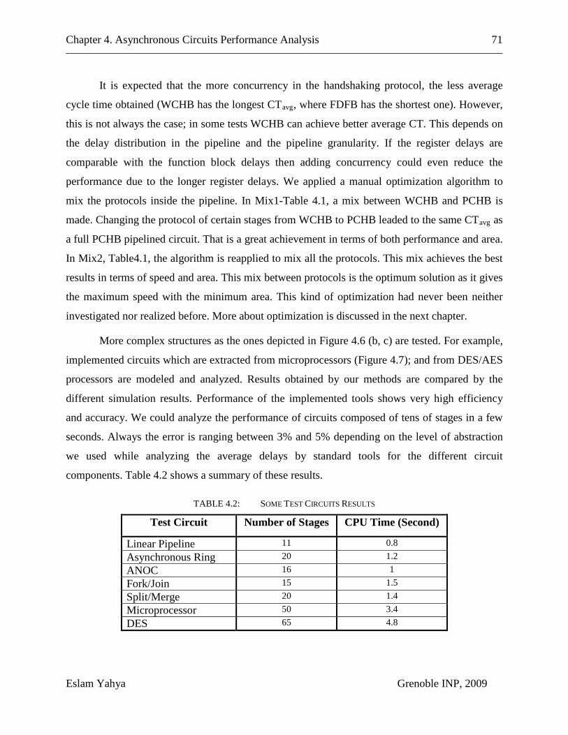
Chapter 4. Asynchronous Circuits Performance Analysis 71
Eslam Yahya Grenoble INP, 2009
It is expected that the more concurrency in the handshaking protocol, the less average
cycle time obtained (WCHB has the longest CTavg, where FDFB has the shortest one). However,
this is not always the case; in some tests WCHB can achieve better average CT. This depends on
the delay distribution in the pipeline and the pipeline granularity. If the register delays are
comparable with the function block delays then adding concurrency could even reduce the
performance due to the longer register delays. We applied a manual optimization algorithm to
mix the protocols inside the pipeline. In Mix1-Table 4.1, a mix between WCHB and PCHB is
made. Changing the protocol of certain stages from WCHB to PCHB leaded to the same CTavg
More complex structures as the ones depicted in Figure 4.6 (b, c) are tested. For example,
implemented circuits which are extracted from microprocessors (Figure 4.7); and from DES/AES
processors are modeled and analyzed. Results obtained by our methods are compared by the
different simulation results. Performance of the implemented tools shows very high efficiency
and accuracy. We could analyze the performance of circuits composed of tens of stages in a few
seconds. Always the error is ranging between 3% and 5% depending on the level of abstraction
we used while analyzing the average delays by standard tools for the different circuit
components. Table 4.2 shows a summary of these results.
as
a full PCHB pipelined circuit. That is a great achievement in terms of both performance and area.
In Mix2, Table4.1, the algorithm is reapplied to mix all the protocols. This mix achieves the best
results in terms of speed and area. This mix between protocols is the optimum solution as it gives
the maximum speed with the minimum area. This kind of optimization had never been neither
investigated nor realized before. More about optimization is discussed in the next chapter.
TABLE 4.2: SOME TEST CIRCUITS RESULTS
Test Circuit Number of Stages CPU Time (Second)
Linear Pipeline 11 0.8 Asynchronous Ring 20 1.2 ANOC 16 1 Fork/Join 15 1.5 Split/Merge 20 1.4 Microprocessor 50 3.4 DES 65 4.8

Chapter 4. Asynchronous Circuits Performance Analysis 72
Eslam Yahya Grenoble INP, 2009
Asynchronous rings are linear pipelines; nevertheless, they need more CPU time for
analyzing them compared to linear pipelines. The reason is the complex models of the Muller
gates in case of asynchronous rings. These models are including Charlie effect which appears in
Equation 4.1. Models for Splits/Merges are more complex than Fork/Joins. However, 20 stages
Split/Merge circuits needs less CPU time compared to 15 stages Fork/Join circuit. Fork/Join
circuits are nondeterministic; where data are propagating unconditionally in all branches.
However data in conditional circuits composed of Splits/Merges propagate only in the selected
branches which is reducing the number of stages that have to be analyzed.
Compared to previous works, our methods have many advantages from different points of
view.
Flexibility: Our methods and tools can easily model and analyze Linear and Nonlinear
structures. We could analyze acyclic pipelines and cyclic pipelines as well; asynchronous rings
are an example for that. To the best of our knowledge, this is the first methodology which
analyzes controlled nonlinear (conditional branches) circuits with no limitation on their
structures. Moreover, as shown in Table 4.1, the method is efficiently able to mix different
handshaking protocols within one circuit. This strengthens the analysis especially when optimal
circuits are targeted. Many of the previous methods restricted the structure to a unique
handshaking protocol for the whole circuit. Regarding delays, we could use average delays when
rough and fast estimation for the performance is needed. That gives our method the advantage of
using average delay as the work done in [6], [26]. We could also implement delay intervals by a
limited number of samples for each DTV; that gives us the advantage as the work done in [10],
[16], [20], [21], [34]. Compared to works supporting variable distributed delays, our method
could support any PDF and even irregular distributions which are measured in the fabrication
line. In [35] distributions are limited to exponential and in [18] they are limited to identical
Gaussian PDFs in all stages. To test the efficiency of the proposed method with different
distributions, we lunched a test on a circuit where we change the length of the Delay Token
Vectors “DTVs” of the circuit components and record the required CPU time, the test is done on
a PC under Windows equipped with an AMD µp running at 2 GHz and 1 GB RAM.. Figure 4.8
depicts the response of the tools with the delay token vector length “L”.

Chapter 4. Asynchronous Circuits Performance Analysis 73
Eslam Yahya Grenoble INP, 2009
0.00001
0.0001
0.001
0.01
0.1
1
10
10 100 1000 10000 100000
DTV Length (L)
CPU
Tim
e in
SEc
s
Figure 4.8: DTV Length (L) Effect on the Method Computation Time
The figure clearly shows a linear growth in the method computation-time with respect to
the DTV length. This property gives our method the advantage of adapting its complexity to the
delay type used inside the system. In comparison to this, previous works which are supporting
delay variability have high overheads when they are used with simple average delays.
Complexity vs Circuit Size: another important property needs to be characterized: the
method complexity vs the circuit size. For evaluating such response, we use a circuit where we
fix the DTV lengths inside the circuit components. After that the number of stages is gradually
increased and the required CPU time is recorded. Figure 4.9 shows the tools response for this
test.

Chapter 4. Asynchronous Circuits Performance Analysis 74
Eslam Yahya Grenoble INP, 2009
0.00001
0.0001
0.001
0.01
0.1
1
10
10 100 1000 10000 100000
Circuit Size (N)
CPU
Tim
e in
Sec
s
Figure 4.9: Circuit Size (N) Effect on the Method Computation Time
The graph shows that the method complexity grows linearly with respect to the circuit
size. The complexity of previous works as in [35], [36] and [50], which are based on Petri nets
and Markov chains, is growing exponentially with the circuit size. The linear response of our
method makes it a practical method for handling large size circuits.
Speed: all the test cases show very fast response of the proposed method. When we
compare the speed of our method with one of the fastest methods which is introduced in [35], we
can record three orders of magnitude enhancement in the computation speed. For instance, in one
test circuit they need 4686.126 Secs for analyzing the circuit. Our tools could analyze the same
circuit in 0.8 Sec which means 5823 times faster response. The machines where the two tests are
lunched are not exactly the same, however, they are still comparable.
Chapter 4. Asynchronous Circuits Performance Analysis 75
Eslam Yahya Grenoble INP, 2009
4.4 Power Consumption Analysis
The Circuit Simulator provides detailed information about the absolute time of the event
occurrence. This information can be collected and analyzed to draw the time profile of the event
activity in the circuit. No doubt each event has equivalent power-consumption (current-
consumption). Using standard tools, the equivalent power-consumption of an event on a certain
component can be extracted. Using this information, the power analyzer is able to map the events
activity to a time distribution of the power consumption. This tool is very efficient in estimating
the power consumption especially in the early phases of the design. Some of the potential
benefits of the power analyzer are:
1) Defining the power hungry parts of the system.
2) Showing the effect of the different handshaking protocols on the event/power-
consumption distribution.
3) Determining the power efficiency in the form of (Power consumed in processing /
Power consumed in registers).
Block diagram of the power analyzer is shown in Figure 4.10. The power analyzer contains a
library which is used for the mapping from events to power consumption. This library is one to
one library mapping that maps component event to power consumption (or current consumption).
Information about the analyzed circuit component should be contained in this library before the
analysis. Absolute time information is passed to the power analyzer which is profiling each
component for the up transition events and down transition events. By means of its library, the
power analyzer could produce a detailed consumption report for the different circuit components.
We characterized some of the TAL library components and STMicroelectronics standard library
components and feed the results in the power analyzer library. As a test, some circuits are
designed using 65 nm. The circuits are analyzed for its power consumption using CADENCE
design flow. Same circuits are modeled and analyzed by our tools; comparison results are shown
in Table 4.3. The test shows that our method calculates the consumed energy in the circuit with
an error < 3%.

Chapter 4. Asynchronous Circuits Performance Analysis 76
Eslam Yahya Grenoble INP, 2009
Power AnalyzerEvent to
Power Consumption Mapping
Power Consumption Metrics
Extracted Delays by Standard Tools
Circuit Structure
Circuit Simulator
Analytical Models For Different Handshaking
Protocols
Absolute Time Info(TTVs)
DTV GeneratorVariability Characteristics
Circuit Simulator
Power Analyzer
Figure 4.10: Connection between the Circuit Simulator and the Power Analyzer
The effect of the protocol on power consumption distribution is discussed in chapter 6.
TABLE 4.3: ENERGY CONSUMPTION IN SOME TEST CIRCUITS
Test Circuit Energy (Analog) Energy (Our Method) Error %

Chapter 4. Asynchronous Circuits Performance Analysis 77
Eslam Yahya Grenoble INP, 2009
Cit1 4.8 E -13 4.78 E -13 2.5 % Cit2 9.15 E -13 8.9 E -13 2.7 %
4.5 Response to Delay Variability
As discussed earlier, one of the main goals of this work is to be able to model circuits
with variable delays. Some circuits of asynchronous ring oscillators are designed and analyzed
for the effect of Within-Die and Die-To-Die process variability. These circuits are designed using
65 nm and 45 nm STMicroelectronics CMOS technology. CADENCE design flow is used for
making the Montcarlo simulations. As depicted in the block diagram of the circuit simulator, the
first step is to characterize the library components for their process variability PDFs. The ring
stage shown in Figure 4.2 is characterized for process variability effect for both Within-Die and
Die-To-Die. Results are shown in Table 4.4.
TABLE 4.4: COMPARISON BETWEEN MONTCARLO ANALYSIS AND OUR METHOD FOR TESTING PROCESS VARIABILITY (TIME VALUES IN PS)
a) Library Characterization for Asynchronous Ring Stage
Within -Die Die-To-Die µ σ µ σ
61.2 1.34 61.3 5
b) Test Case Results
M.C. (103 Methods (10) 5 Err % ) Eff
µ
WD
σ
WD
CPU
WD
µ
DD
σ
DD
CPU
DD
µ
WD
σ
WD
CPU
WD
µ
DD
σ
DD
CPU
DD
µ σ
1225.2 6.1 16595 1227.8 98.8 16024 1224.3 6 1.2 1226.2 99.1 1.2 0.1% 0.95% 13641
The characterization of asynchronous ring stage shows that it has a Gaussian distribution
for its delay under the effect of process variability. In Table 4.4 (a), the first column shows the
Mean (µ) and Standard Deviation (σ) in case of Within Die variability. The second column shows
their values in case of Die-To-Die variability. The mean is almost the same in the two cases;
however, the standard deviation is larger in case of Die-To-Die variation. This result is logical as
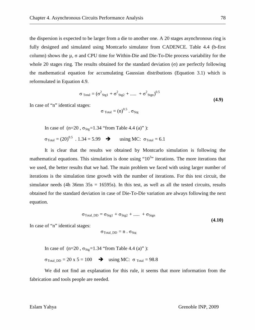
Chapter 4. Asynchronous Circuits Performance Analysis 78
Eslam Yahya Grenoble INP, 2009
the dispersion is expected to be larger from a die to another one. A 20 stages asynchronous ring is
fully designed and simulated using Montcarlo simulator from CADENCE. Table 4.4 (b-first
column) shows the µ, σ and CPU time for Within-Die and Die-To-Die process variability for the
whole 20 stages ring. The results obtained for the standard deviation (σ) are perfectly following
the mathematical equation for accumulating Gaussian distributions (Equation 3.1) which is
reformulated in Equation 4.9.
σ Total = (σ2Stg1 + σ2
Stg2 + ..... + σ2Stgn)
0.5
In case of “n” identical stages: σ Total = (n)0.5 . σ
Stg
(4.9)
In case of (n=20 , σStg
σ
=1.34 “from Table 4.4 (a)” ):
Total = (20)0.5 . 1.34 = 5.99 using MC: σTotal
It is clear that the results we obtained by Montcarlo simulation is following the
mathematical equations. This simulation is done using “10
= 6.1
3
σ
” iterations. The more iterations that
we used, the better results that we had. The main problem we faced with using larger number of
iterations is the simulation time growth with the number of iterations. For this test circuit, the
simulator needs (4h 36mn 35s = 16595s). In this test, as well as all the tested circuits, results
obtained for the standard deviation in case of Die-To-Die variation are always following the next
equation.
Total_DD = σStg1 + σStg2 + ..... + σ
Stgn
In case of “n” identical stages: σTotal_DD = n . σ
Stg
(4.10)
In case of (n=20 , σStg
σ
=1.34 “from Table 4.4 (a)” ):
Total_DD = 20 x 5 = 100 using MC: σ Total
We did not find an explanation for this rule, it seems that more information from the
fabrication and tools people are needed.
= 98.8

Chapter 4. Asynchronous Circuits Performance Analysis 79
Eslam Yahya Grenoble INP, 2009
Same test suite is done using our tools. Results are shown in Table 4.4 (b-second column).
Comparing σ obtained by our method by the one from MC, we see that we have more accuracy
than MC (if the reference is the value obtained by Equation 4.9). We used (105) samples
compared to (103
) samples used for the MC simulation; that explains the enhancement in the
accuracy. Comparing the simulation time needed by our tools (1.2 Secs) to the time needed by
the MC simulation (16595 Secs) and even if we are using more samples, our tools show five
orders of magnitude improvement in the simulation time. The efficiency of using our tools is
calculated in Table 4.4 (b-fourth column). The accuracy of the results obtained by our tools (if
the MC results are the reference) is shown in Table 4.4 (b-third column); our tools have less than
1% error.
4.6 Conclusion
In this chapter, absolute time information of the circuit events is used to analyze the
circuit performance from different points of view.
First, a methodology for analyzing the time performance of asynchronous circuits is
described. This method is implemented and then applied to different test circuits which are
extracted from real implemented systems. Some analog phenomena known as Charlie effect is
briefly discussed. This phenomenon affects cyclic circuits (as asynchronous rings) and looped
circuits (as iterative looped DES). Our models are designed for considering this phenomenon
when necessary. Our methods and tools show flexibility with different circuit structures, mixing
handshaking protocols in a single circuit and using different delay types. One of the important
advantages of the proposed method is the linear growth of its complexity with respect to circuit
size. This property makes our tools much faster than the previously introduced works. Our tools
could reach three orders of magnitude enhancement in simulation time WRT previous works. The
accuracy of the proposed methods is evaluated by a comparison with analog and timed VHDL
simulations. Our methods give results with an error which is less than 5% compared to other
simulation methods.

Chapter 4. Asynchronous Circuits Performance Analysis 80
Eslam Yahya Grenoble INP, 2009
Second, a method for converting the circuit events into current/power consumption
information is used. By means of this method we built a power analyzer which is able to estimate
the power consumption and its distribution in time. The use of the power analyzer is
demonstrated by some examples. When comparing the energy consumption obtained by our
analyzer with those obtained by CADENCE flow, we can see an error less than 3% in our results.
The use of the power analyzer for profiling the time distribution of the power consumption is
discussed in next chapters.
Finally, we showed how it is efficient to use our methods for analyzing process
variability. The methods could analyze Within Die and Die To Die process variation with very
high accuracy. In comparison with Montcarlo simulator, our tools showed five orders of
magnitudes enhancement in the simulation time with an error which is less than 1%.
Unfortunately we could not make the comparison using considerably large circuits due to the
huge computation time and resources needed by the Montcarlo simulation.
Parts of the work presented in this chapter are published in [54] [56] [65] [64].

81
Eslam Yahya Grenoble INP, 2009
Chapter 5. Asynchronous Circuits Performance Optimization
5.1 Introduction
The developed modeling and analysis methods are providing fast and accurate timing
analysis. Next step is to use these methods for guiding optimization of the analyzed circuit. There
are two main approaches in optimizing asynchronous circuits. The first approach is to develop
synthesis flow which is optimizing the mapping from the specification to the circuit
implementation [25]. The other approach is to use timing analysis method to guide some
structure changes which lead to an optimized implementation [26]. The optimization method
proposed in [26] is based on pipeline optimization. The idea is to find the minimum pipelining
degree to satisfy the performance constraints. That means using the minimum number of registers
which reduces the pipeline area and power consumption for a given performance. The
optimization technique introduced in this chapter can be classified in the same category.
The problem addressed in this chapter is the problem of a designer having asynchronous
pipelines where time delay variability can be taken into account. The designer needs to answer
two questions: “Targeting certain performance, what is the minimum number of asynchronous
registers that should be used? And, what is the optimum placing of these registers which not only
satisfies the target performance, but also results in the maximum possible performance using this
number of registers?” The answers to these two questions are the contribution of this chapter.
5.2 Pipeline Optimizer.
Figure 5.1 shows the connections between the Optimizer, the Circuit simulator and the
Timing analyzer. As shown in the figure, the optimization starts with a circuit specification
which contains the minimum number of registers those are needed to keep the circuit a live (no
deadlocks). The designers define their Cycle Time “CT” constraints to the optimizer. The circuit
simulator analyzes the initial structure and passes the output TTVs to the Timing Analyzer. The
Timing Analyzer solves the circuit cycle time and passes the results to the Optimizer. After that,
the Optimizer compares the circuit cycle time with the targeted cycle time. By applying certain

Chapter 5. Asynchronous Circuits Performance Optimization 82
Eslam Yahya Grenoble INP, 2009
algorithms, the optimizer estimates a suggested structure which might enhance the circuit
performance. This suggested structure is passed to the Circuit Simulator which analyzes the new
circuit structure and the cycle continues. Finally the Optimizer ends with the optimum circuit
structure which satisfies the targeted cycle time with the minimum number of registers. In
addition, this optimum structure defines the placement of the registers so that the circuit reaches
the maximum possible cycle time with this number of registers; that enhances the HW utilization.
Extracted Delays by Standard Tools
Circuit Structure(minimum Registers)
Circuit Simulator
Analytical Models For Different Handshaking
Protocols
Absolute Time Info(TTVs)
Delay Generator
Timing Analyzer
Timing-Metrics Equations
Timing PerformanceMetrics
Optimizer
Circuit Structure(Minimum Registers)
SuggestedStructure
Cycle Time
Cycle Time Constraints
Optimum Structure
Figure 5.1: The Tool Flow Including the Optimizer
It is clear that the optimizer is calling the performance analysis tool for many times until
the optimum structure is found. This means that the final computation time needed to find the

Chapter 5. Asynchronous Circuits Performance Optimization 83
Eslam Yahya Grenoble INP, 2009
optimum structure is not only determined by the optimizer but also by the time response of the
underlying performance analysis tool.
5.3 Optimal (Brute Force) Algorithm.
Before going deeply in the algorithms, it is needed to explain the problem to be solved
and some of its terminology. Figure 5.2 depicts Asynchronous pipeline before and after
optimization. The pipeline with the minimum number of registers which are necessary to keep the
liveness of the pipeline is shown in Figure 5.2 (a). This pipeline needs at least two registers at the
input and output (R0 and Rn
) to handle the interaction with the environment. In this pipeline there
are some possible places, denoted (P), to place the registers. These places are predetermined and
fixed inside the structure. That means that our algorithm does not perform retiming (in the sense
of breaking or merging function blocks). The Optimizer searches the minimum number of
registers which are needed to satisfy a given performance and find where to insert these registers
between the function blocks. In the figure there are seven places (P=7). Register1 (R1) and
Register2 (R2) are placed in places P2 and P6 respectively. The Stage consists of one register
with all its preceding Function Blocks. As an example, Stage2 (Stg2) consists of R2 plus (F5, F4,
F3, F2).

Chapter 5. Asynchronous Circuits Performance Optimization 84
Eslam Yahya Grenoble INP, 2009
TX F1 F2 F3 F4 F5 F6 RX
P1 P2 P3 P4 P5 P6 P7R0 Rn
TX F1 F2 F3 F4 F5 F6 RX
P1 P2 P3 P4 P5 P6 P7R0 Rn
TX F1 F2 F3 F4 F5 F6 RX
P1 P2 P3 P4 P5 P6 P7
Stage1 (Stg1) Stage2 (Stg2)
R1 R2
R0 Rn
TX F1 F2 F3 F4 F5 F6 RX
P1 P2 P3 P4 P5 P6 P7
Stage1 (Stg1) Stage2 (Stg2)
R1 R2
R0 Rn
(a) Asynchronous Pipeline with the Minimum Number of Registers
(b) The Circuit After Adding Some Registers
Figure 5.2: Asynchronous Circuit Optimization by Controlling Number of Registers
Please recall that each component in the circuit, (F, R, TX and RX), has its own Delay
Token Vector (DTV). The DTV Length is denoted by “L”. Each component will have Average,
Min and Max delays which are representing the average value of the whole DTV, the minimum
value of the whole DTV and the maximum value of the whole DTV, respectively. Taking
function block F3 as an example these delays will be respectively denoted as (DF3Avg, DF3
Min,
DF3Ma x
∑=
=
=5
2
2
1
i
i
FiAvg
Avg
R
RDDt
). Here we define a new performance metric it is the Distance between two registers “Dt”.
The distance between two registers is “the sum of the delays in-between them; in other words, it
is the latency between them”. As an example, the average distance between R1 and R2 in Figure
5.2 (b) can be expressed as shown in Equation 5.1.
(5.1)

Chapter 5. Asynchronous Circuits Performance Optimization 85
Eslam Yahya Grenoble INP, 2009
The problem the optimizer is solving is as follows. Given a pipeline structure that has
possible places “P” and a cycle time in case of only necessary registers are placed “CTNR”, the
optimizer finds a minimum number of registers “η” for which the pipeline’s CT satisfies a target
cycle time constraints “CTT”. Moreover, the optimizer finds the optimum placing for the “η”
registers among the possible places “P”. It ends with “ηOpt” such that the pipeline’s CT is not
only satisfying CTT
A straightforward way to implement the optimizer is to do an exhaustive search for all the
possible η (from η=1 to η=P), and for each η the algorithm tests all the possible placing of the η
registers among the P places “
, but is also the minimum cycle time, Max throughput, that can be achieved
using the “η” registers.
Cη
P ”. With such a Brute Force (BF) algorithm, it is guaranteed that
the optimizer will find “ηOpt” for any requested CTT (once this CTT
BF
is achievable by placing
“η≤P” registers). The complexity (number of iterations) of the BF algorithm is shown in Equation
5.2.
Iterations = 2 (5.2) P
Hereafter is the pseudo code of the BF algorithm.
{
For (η = 1 → η = P)
{
Test all Cη
P and pick the one giving the least CT “ηOpt
}
”;
Out the min ηOpt where CT ≤ CTT
};
;

Chapter 5. Asynchronous Circuits Performance Optimization 86
Eslam Yahya Grenoble INP, 2009
Because this algorithm is enumerating all the possible structural combinations, we are
formally sure that this algorithm ends with optimum solution. Our basic goal is to develop an
algorithm which is proven formally to end with the optimum circuit structure.
One simple, but efficient, optimization is possible to be applied to the BF algorithm. Due
to the nature of the problem, the lower the numbers of registers “η”, the better the solution. This
means that if we could reach CTT with η = 3, for example, so no need to test the cases where
(3<η≤ P). In this way, we avoid unnecessary testing for greater values of η. Meanwhile, we are
formally sure that the resultant η is the “ηOpt
For ( η = 1 → η = P )
”. Hereafter, the pseudo code of this simple
optimized algorithm, it will be denoted by the Reference Algorithm “RA”.
{
Test all Cη
P and pick the one giving the least CT (ηOpt
If (CT ≤ CT
) ;
T
};
) Break ;
As shown in Figure 5.1, the optimizer calls the Circuit Simulator and the Timing
Analyzer for each suggested structure. Consequently, its complexity determines the final
execution time needed for optimizing the circuit. Equation 5.3 gives the complexity of the RA.
∑∑=
=
=
= −×==
ηη i
i
i
i
i
PItrations iPiPRA C
11 )!(!!
(5.3)
The BF algorithm and the RA are implemented in the Optimizer appears in Figure 5.1.
Many test cases were conducted to test the algorithms and their implementation. In one test case,
a pipeline as the one depicted in Figure 5.2 (a), is designed. This pipeline contains 11-function
blocks plus TX and RX, that means that P=12. Delay TVs are time variable probabilistic delays,
different probabilistic distributions are used. The design is analyzed and optimized targeting
many different cycle times. Figure 5.3 shows a comparison between the BF algorithm and the RA

Chapter 5. Asynchronous Circuits Performance Optimization 87
Eslam Yahya Grenoble INP, 2009
in terms of number of iterations needed to determine ηOpt. The X-axis represents 36 different CT
values in which the CTT
No of Iterations
0
500
1000
1500
2000
2500
3000
3500
4000
4500
1 3 5 7 9 11 13 15 17 19 21 23 25 27 29 31 33 35
BF RA
is decreasing. The Y-axis represents the number of iterations.
Figure 5.3: Number of Iterations for BF and RA
Compared to BF, EA has much better performance for high CT, equivalently lower η. It is
explained by the fact that when η is low, EA gets the solution early and prunes many unnecessary
iterations. Same contribution can be derived from Equations 5.2 and 5.3.
Table 5.1 shows a comparison between the BF and the RA in terms of the average
number of iterations needed to solve the 36 CTT
TABLE 5.1: TOTAL ITERATIONS AND CPU TIMES IN BF AND RA (TIME VALUES IN SEC)
in the test case of Figure 5.4. The RA
introduces a gain of 42.7% in terms of number of iterations compared to the BF algorithm.
Technique Iterations Gain% WRT BF
Brute Force (BF) 4095 - Reference Algorithm (RA) 2346 42.7%

Chapter 5. Asynchronous Circuits Performance Optimization 88
Eslam Yahya Grenoble INP, 2009
Regarding the algorithm computation time, the RA needs 703.2 Sec to find ηopt
5.4 Efficient-Optimal Algorithms.
for 12
possible places (P=12) where each function block has a probabilistic time variable delays with a
DTV length of L=10^5 tokens (execution times are measured on A SPARC III machine with
2GB of Ram).
The Brute Force algorithm is a way to enumerate all the possible solutions and pick the
optimum one. However, this algorithm is very costly from the execution-time point of view. The
RA is better in terms of execution time and it is still giving an optimum solution. However, the
RA is efficient only when the final solution is among the first 2 or 3 values of P. According to
Equation 5.3, its execution time grows exponentially with the values of P. More efficient
algorithms are needed. One possible way to strongly enhance the performance of the RA is to
apply the Branch and Bound technique (BB).
Branch and Bound (BB): is a general algorithm for finding optimal solutions of various
optimization problems. It consists of a systematic enumeration of all candidate solutions, where
large subsets of fruitless candidates are discarded, by using upper and lower estimated bounds of
the quantity being optimized.
The problem of finding the minimum number of registers “η” and finding the optimum
placing “ηOpt
],1[ P∈η
” can be seen as a two-dimensional problem. The first dimension is to find η
where: . This dimension appears in the pseudo code of Section 5.3, in the main outer loop.
As a result we call it Outer Loop “OL”. For each suggested η, there is an inner loop enumerating
all possibilities for placing η registers among P places. This loop is the second dimension of the
problem and it is called the Inner Loop (IL). Optimizing both OL and IL can of course
significantly enhance the algorithm performance.
5.4.1 Outer Loop Optimization (OL)
It is simpler to start with the outer loop and apply the BB technique. The problem will be
enumerated so that the algorithm tests all the possible values for ],1[ P∈η . Now, an efficient
bounding criteria need to be defined to eliminate some non-promising possibilities of η.

Chapter 5. Asynchronous Circuits Performance Optimization 89
Eslam Yahya Grenoble INP, 2009
Therom1: For any linear pipeline, if the max internal delay of the registers “R” is lower
than the min delay of the Function Blocks “F”, then adding registers to a linear pipeline is
increasing the throughput monotonically. In other words, increasing the number of registers is
decreasing the cycle time of the pipeline.
R1 F1 R2F2
R1 F1 R2F2
R1 F1 R2F2
R1 F1 R2F2
R3
R3a b
R1 F1 R2F2
R1 F1 R2F2
R1 F1 R2F2
R1 F1 R2F2
R3
R3a b
Figure 5.4: Dependencey Graph Explaining Breaking a Stage by Adding a Register
Proof1: Figure 5.4 (a) shows the dependency graph of a stage which contains 2 cascaded
function blocks (F1,F2
DDDDDtCT RFFRR
R
22111
21+++==
). The CT of the stage is:
If register R3
)](); 223311
2 [( DDDDDDMaxCT RFRRFR++++=
is added in between F1 & F2, as in Figure 5.4 (b), the CT becomes:
If: DDD RFR 223 +≤ & DDD FRR 113 +≤
CTCT 12 ≤∴ Adding a register is a monotonic problem.
IF DMinDMax Fj
Min
Pj
j
Ri
Max
i
i
=
=
<
=
= 11
η
(5.4)
Then η↑ → CT↓ and η↓ → CT↑
In words, “If the maximum delay of any register is less than the minimum delay of any
function block then adding registers to the pipeline will decrease the cycle time”. This means that

Chapter 5. Asynchronous Circuits Performance Optimization 90
Eslam Yahya Grenoble INP, 2009
if the condition in Equation 5.4 is satisfied, adding registers to the pipeline is guaranteed to affect
the cycle time monotonically. This is an important property which helps the designers to simplify
their circuit optimization.
If the algorithm starts searching the outer loop using an initial guess for η where: η = ηi ,
comparing the optimum CT in case of ηi with the target CTT will lead us to either increase or
decrease ηi . As a result either (ηi - 1) or (P - ηi) possible values of η are pruned. Depending on
the accuracy of the initial guess, the total number of iterations can be significantly reduced.
Hereafter the pseudo code of the algorithm which is using initial guess for the number of registers
(ηi
{ η = η
).
Test all
i
Cη
P and pick the one giving the least CT (ηOpt
η = η
) ;
Opt
Compare resultant CT by CT
;
{
T
If (CT = CTT
If (CT < CT
) Then (out η and break)
T) Then (Start = 1 and End = ηi
If (CT > CT
) “decrease number of registers”
T) Then (Start = ηi
}
+1 and End = P) “increase number of registers”
For ( η = Start → η = End )
{
Test all Cη
P and pick the one giving the least CT (ηOpt
If (CT ≤ CT
) ;
T
};
) Break ;
}

Chapter 5. Asynchronous Circuits Performance Optimization 91
Eslam Yahya Grenoble INP, 2009
Proof2 (optimality of the OL optimization): if the circuit satisfies the condition stated
in Equation 5.4, it is sure that the cycle time is monotonic with respect to the pipelining degree
(η↑ → CT↓ and η↓ → CT↑). Since the algorithm searches all the possibilities of the initial
guess ηi and then decides to either increases or decreases η. In both cases the algorithm slides η
and studies all the possible structures. As a result, no doubt that the algorithm finds the minimum
η. Due to the fact that the inner loop is responsible for finding the optimum placing, OL
optimization has no effect on ηOpt
Guessing an initial value η
. To conclude, the optimizer after applying the OL
optimization, under the condition in Equation 5.4, is finding the optimum solution.
i, which is near to the final solution, is the key parameter to
increase the outer loop efficiency. However, it is not an easy task to accurately guess this initial
value. In an asynchronous pipeline, there are very complex relations between all circuit
components. The behavior of the pipeline is affected by the handshaking protocol implemented in
the registers and the delay values in all the components. When time variable delay values are
considered, especially if they are probabilistic, circuit behavior becomes very complex and even
impossible to be predicted. Here after, many strategies to choose an initial degree of the pipeline,
ηi
CT
, are investigated.
NR/CTT: in an ideal pipeline, where all stages are identical in their delays, a perfect
estimation for the degree of pipeline is to divide (integer division) the cycle time of the structure
with only the necessary registers CTNR, by the target cycle time CTT
η
.
i = CTNR/CT (5.5) T
(CTNR/CTT)+1: in the above estimation, ηi
η
takes the integer of the division result. Here,
one is added to that integer.
i = (CTNR/CTT (5.6) ) + 1
Avg: the above estimations of ηi are very simple and optimistic. More realistic strategy is
needed. To achieve that, the estimation should be based on the real delays of the pipeline stages.
One possible way is to consider the average delay value of each function block. Using that
average and starting from the TX, the average delay is accumulated and when it violates CTT, a

Chapter 5. Asynchronous Circuits Performance Optimization 92
Eslam Yahya Grenoble INP, 2009
register is added. The resultant number of registers is taken as ηi
For ( i = 1 → i = P )
. The following pseudo code
describes this strategy.
{
Delay = Delay + DFiAvg ;
If (Delay > CTT
{
)
η = η + 1 ;
Delay = DFiAvg ;
}
}
Max and Min: in fact the average delays are relevant in case of static time average delays
or time variable delays with very long TVs. In case of short deterministic TVs it may not be the
best choice. Estimation can be done using the maximum or the minimum delay value in the TV
of each circuit component. In this case extremely pessimistic/optimistic estimation is done. The
change in the above pseudo code would be the use of DFi
Max or DFi
Min instead of DFi
Avg when
calculating ηi
(Max+Min)/2: in this strategy, η
.
i
DFi
Max
is the average between the initial guess calculated using
and calculated using DFi
Min. this is not equivalent to the case of average delay. In case of
average delay the estimation is based on the average value of the DTVs ( DFi
Avg).
One question can be raised here: what is the cost of the initial guess based on average,
min and max; especially in case of very long DTVs as in probabilistic time variable delays? In
fact managing this point in the implementation is quite important. In the implemented tools,

Chapter 5. Asynchronous Circuits Performance Optimization 93
Eslam Yahya Grenoble INP, 2009
average, max and min are calculated and saved while reading the TVs. As a result, depending on
them to calculate the initial guess has almost no running-cost during the algorithm computation.
A pipeline as the one depicted in Figure 5.2 (a), is designed. This pipeline contains 11-function
blocks plus TX and RX, that means that P=12. The design is analyzed and optimized targeting
many different CTs. Fig.4 shows a comparison between the different proposed OL optimization-
strategies in terms of number of iterations needed to determine ηOpt. The X-axis represents 36
different CT values in which the CTT
0
500
1000
1500
2000
2500
3000
3500
4000
4500
1 2 3 4 5 6 7 8 9 10 11 12 13 14 15 16 17 18 19 20 21 22 23 24 25 26 27 28 29 30 31 32 33 34 35 36
BF RA CTNR/CTT (CTNR/CTT)+1
CTT
No.
of I
tera
tions
0
500
1000
1500
2000
2500
3000
3500
4000
4500
1 2 3 4 5 6 7 8 9 10 11 12 13 14 15 16 17 18 19 20 21 22 23 24 25 26 27 28 29 30 31 32 33 34 35 36
BF RA CTNR/CTT (CTNR/CTT)+1
CTT
No.
of I
tera
tions
is decreasing. The Y-axis represents the number iterations
required to reach the target CT.

Chapter 5. Asynchronous Circuits Performance Optimization 94
Eslam Yahya Grenoble INP, 2009
0
500
1000
1500
2000
2500
3000
3500
4000
4500
1 2 3 4 5 6 7 8 9 10 11 12 13 14 15 16 17 18 19 20 21 22 23 24 25 26 27 28 29 30 31 32 33 34 35 36
BF AVG Max Min (Max+Min)/2
No.
of I
tera
tions
0
500
1000
1500
2000
2500
3000
3500
4000
4500
1 2 3 4 5 6 7 8 9 10 11 12 13 14 15 16 17 18 19 20 21 22 23 24 25 26 27 28 29 30 31 32 33 34 35 36
BF AVG Max Min (Max+Min)/2
No.
of I
tera
tions
Figure 5.5: A Comparison Between Diferrent Heuristics in the OL Optimization
The curve “BF” in Figure 5.5, represents the iterations of the Brute Force algorithm, this
curve is constant in the entire graph (2P). The second curve RA represents the response of the
reference algorithm. All the other curves represent the number of iterations after applying one of
the OL-optimization heuristics presented in this section. As it is clear from the figure, it is hard to
say which initial guess strategy is the best. For example, the “Max” strategy needs more
iterations compared to the other strategies at high CTT (the beginning of the curves). However it
gives the best results in case of low CTT
. In general, applying the OL optimization gives
significant enhancement compared to the BF algorithm.
5.4.2 Inner Loop Optimization (IL)
For each run of the OL the IL tests “Cη
P” different structures. Indeed some of these
structures are non-promising. Again the BB technique is applied to optimize this loop. The goal

Chapter 5. Asynchronous Circuits Performance Optimization 95
Eslam Yahya Grenoble INP, 2009
is to find a bound that is able to prune some of the non-promising structures without affecting the
optimality of the solution. The distance between registers, Dt, can be a useful property to prune
some non promising solutions. If the minimum distance between any two suggested places for
inserting registers is larger than CTT
CTDtMax TMin
Ri
Ri
i
i>
+=
=
1
1
η
, then it is sure that this solution is not feasible and can be
safely discarded. This condition is shown in Equation 5.7.
(5.7)
Using the condition in Equation 5.7 as abound, a BB technique is applied to optimize the
IL. The condition is tested and whenever it is true for the suggested structure, the algorithm
discards this structure and avoids analyzing it. Same test case as the one in the previous
subsection is repeated while optimization for both IL and OL are applied. Figure 5.6 shows the
number of iterations for each heuristic.
0
500
1000
1500
2000
2500
3000
3500
4000
4500
1 2 3 4 5 6 7 8 9 10 11 12 13 14 15 16 17 18 19 20 21 22 23 24 25 26 27 28 29 30 31 32 33 34 35 36
BF RA CTNR/CTT (CTNR/CTT)+1
CTT
No.
of I
tera
tions
0
500
1000
1500
2000
2500
3000
3500
4000
4500
1 2 3 4 5 6 7 8 9 10 11 12 13 14 15 16 17 18 19 20 21 22 23 24 25 26 27 28 29 30 31 32 33 34 35 36
BF RA CTNR/CTT (CTNR/CTT)+1
CTT
No.
of I
tera
tions

Chapter 5. Asynchronous Circuits Performance Optimization 96
Eslam Yahya Grenoble INP, 2009
0
500
1000
1500
2000
2500
3000
3500
4000
4500
1 2 3 4 5 6 7 8 9 10 11 12 13 14 15 16 17 18 19 20 21 22 23 24 25 26 27 28 29 30 31 32 33 34 35 36
BF Avg Max Min (Max+Min)/2
No.
of I
tera
tions
0
500
1000
1500
2000
2500
3000
3500
4000
4500
1 2 3 4 5 6 7 8 9 10 11 12 13 14 15 16 17 18 19 20 21 22 23 24 25 26 27 28 29 30 31 32 33 34 35 36
BF Avg Max Min (Max+Min)/2
No.
of I
tera
tions
Figure 5.6: The Algorithm Performance After Applying Optimization to both IL and OL
By comparing Figure 5.5 and Figure 5.6, benefits of applying the IL optimization are
clear. In Table 5.2 and Table 5.3, results of the test case of Figure 5.5 and Figure 5.6 are shown
respectively. The column “Iterations” represents average number of iterations needed to achieve
the different targeted CTT. The column “Gain% WRT BF”, is the percentage of the gain
introduced by each heuristic compared with the Brute Force algorithm. The column “Gain%
WRT RA”, is the percentage of the gain introduced by each heuristic compared with the
reference algorithm. Some figures of the optimizer execution time are shown in Table 5.3. These
execution times are measured on A SPARC III machine with 2GB of Ram. Generally speaking,
the OL optimization is contributing more than the IL optimization. Inspecting Figures 5.5 and 5.6
in addition to results presented in the tables, IL optimization is able to correct the behavior of the
OL optimization when it is too bad, as in case of heuristic based on “Min”. Before applying IL
optimization the gain was less than 1% compared to the RA, however it is increased to 25% after
the IL optimization. In general, applying both optimizations can result in an average gain of 50%
WRT RA and more than 70% WRT BF. This means a computation time reduction of nearly the
same percentage.

Chapter 5. Asynchronous Circuits Performance Optimization 97
Eslam Yahya Grenoble INP, 2009
TABLE 5.2: RESULTS AFTER APPLYING OL OPTIMIZATION
Technique Iterations Gain% wrt BF Gain% WRT RA
Brute Force (BF) 4095 - Reference Alg (RA) 2346 42.7 -
CTNR/CTT 1682 58.9 28.2 (CTNR/CTT)+1 1315 67.9 43.9
Avg 1254 69.3 46.5 Max 1408 67 40 Min 2326 43.1 0.87
(Max+Min)/2 1328 67.6 43.40
TABLE 5.3: RESULTS AFTER APPLYING OL AND IL OPTIMIZATION
Technique Iterations Gain% wrt BF Gain% WRT RA CPU Time (Sec)
Brute Force (BF) 4095 - Reference Alg (RA) 2346 42.7 - 703.8
CTNR/CTT 1549 62.2 33.9 464.7 (CTNR/CTT)+1 1267 69.1 46 380.1
Avg 1177 71.3 49.8 353.1 Max 1351 65.6 42.4 405.3 Min 1758 57.1 25 527.4
(Max+Min)/2 1173 71.3 49.99 351.9
The average number of iterations is considered just to give a unique figure for each
strategy of estimating ηi. However, it is clear that no method is always the best solution as it
depends on the value of CTT. Moreover, these figures are related somehow to the examples. That
means these figures may vary with another configuration of the test circuit. Generally speaking,
ηi which is based on average rules, “Avg” and “(Max+Min)/2”, are more promising. However, in
any particular example, it depends on the value of CTT
Regarding the algorithm computation time, the last column in Table 5.3 gives the average
computation time for each optimization technique. The table shows how our optimizer is fast. On
the average, it needs around 6 minutes to find η
and the circuit properties.
opt for 12 possible places (P=12) where each
function block has a probabilistic time variable delays with a TV length of M=10^5 tokens. To
the best of our knowledge, the nearest work to the presented work in this chapter is the work
introduced in [26]. The main difference between the two works is that in [26], only average
delays are supported. It means that each component in the circuit is assigned a single delay value,

Chapter 5. Asynchronous Circuits Performance Optimization 98
Eslam Yahya Grenoble INP, 2009
and no time variability could be considered. In contrast, our work supports all types of delay
including probabilistic delays. Regarding the performance, in their paper they stated that their
algorithm needs 650 Millisec to pipeline a circuit having 15 places with 2 registers initially
placed. In comparison, our tool needs 354 Microsec to solve the test case example (12 places
with no initially placed registers) if average delays are considered. The comparison remains
difficult because we could not find the machine specification they used; however, based on the
data, our method seems to faster by around three orders of magnitude.
5.5 Optimizing ANOC Link between Two Synchronous Processors.
As another illustrative example, a dedicated asynchronous communication link between
two synchronous microprocessors in ANOC system is considered. This circuit is a coarse grain
structure as the delays of the routers are quite large compared to the delays of the registers. This
coarse grain granularity demonstrates well the effect of adding registers to the pipeline.
Moreover, the condition in Equation 5.4 is certainly applicable in this case. The example consists
of two synchronous microprocessors which are communicating using Asynchronous NOC link.
As shown in Figure 5.7, both processors have Sync/Async interfaces to handle the conversion
between the processors and the link. The goal is to optimize the communication channel which
transfers data from Processor-A (MP-A) to Processor-B (MP-B). The clock frequency of MP-A is
set to 500 MHz whereas the clock frequency of MP-B is set to 400 MHz. Both processors
emit/receive data bursts. Output/Input characteristics of MP-A/MP-B are modeled using
deterministic delays (where they have a train of data bursts separated by some waits; this pattern
is repeated periodically). Data bursts are modeled using DTVs so that the average data rate on
both sides is 100 M/Sec. However, data bursts on both sides are not synchronized. Which means
MP-A could be ready for sending data, however, MP-B is not ready to receive them. This makes
the task of the link more complex and justifies the need for pipelining this link.

Chapter 5. Asynchronous Circuits Performance Optimization 99
Eslam Yahya Grenoble INP, 2009
MP-A
500 MHz
Sync/
Async
MP-B
400 MHzF1
P2
F2
P3
F..
P..
F15
P16P1
Async/
Sync
MP-A
500 MHz
Sync/
Async
MP-B
400 MHzF1
P2
F2
P3
F..
P..
F15
P16P1
Async/
Sync
Figure 5.7: The Algorithm Performance After Applying Optimization to both IL and OL
The route between the two MPs is modeled as a pipeline where the routers are modeled as
the function block. This pipeline is predefined with 16 possible places to add asynchronous
registers; that gives us a problem of a pipeline with P=16. The goal is to optimally pipeline this
communication channel to satisfy different given CTs. Note that pipelining such an asynchronous
link, locally amplifies the signals and at the same time inserts registers in a FIFO like manner
which speeds up the communication throughput.
First of all, the communication rate between the two processors, when they directly
communicate without any register, is determined using the performance analysis tool. The
average CT obtained is 71.185ns, i.e. a communication rate of 14 MHz even though both
processors can afford a 100 MHz communication rate. The limitation in the communication rate
comes from the unmatched data bursts and the router delays. This result shows that the
communication channel needs registers to speed up the rate. The process variability PDF is
investigated and equivalent probabilistic time variable delays are assigned to the pipeline
registers and the routers (function blocks). The Out/In timing characteristics of the two
processors are modeled as deterministic delays in MP-A and MP-B. The designer question now
is: targeting a given cycle time “CTT”, what is the minimum number of registers he should use to
pipeline the channel between the processors? And, what is the optimum placing of these registers
which not only satisfies the CTT
Different CT
, but also results in the minimum possible CT using this number
of registers?
T are targeted, CTT is gradually decreased from the maximum (no register =
71 ns) to the minimum achievable with 16 registers. Table 5.4 shows the values of CTT with the

Chapter 5. Asynchronous Circuits Performance Optimization 100
Eslam Yahya Grenoble INP, 2009
corresponding η. A comparison between the Brute Force algorithm, Reference algorithm and an
optimization based on the average criterion is depicted in Figure 5.8. ANOC Link Optimization
TABLE 5.4: ANOC LINK OPTIMIZATION
η CTT (ns) RA Avg η CTT (ns) RA Avg 1 40.9 16 688 9 14.2 50642 31674 2 29.8 136 2343 10 13.7 58650 39286 3 25 696 1967 11 13.1 63018 43565 4 21.7 2516 1602 12 12.7 64838 37003 5 19.1 6884 4266 13 12.5 65398 22328 6 17.1 14892 8176 14 12.2 65518 22448 7 16.4 26332 15638 15 11.6 65534 20175 8 15 39202 23769 16 11 65535 20176
0
10000
20000
30000
40000
50000
60000
70000
1 2 3 4 5 6 7 8 9 10 11 12 13 14 15 16
BF RA Avg
CTT
No.
of I
tera
tions
0
10000
20000
30000
40000
50000
60000
70000
1 2 3 4 5 6 7 8 9 10 11 12 13 14 15 16
BF RA Avg
CTT
No.
of I
tera
tions
Figure 5.8: Optimization Algorithm Performance for ANOC Link between Two Microprocessors
In Table 5.4, the two columns titled “RA” and “Avg”, are showing the number of
iterations for the reference algorithm and the optimized algorithm (both OL and IL optimization
are applied). In the table, the strategy used for OL optimization is based on average delays. The
minimum CT that can be achieved using P=16 is “11 ns” which is a bit less than the ideal case
“CT=10 ns” to fully utilize the communication rates afforded by the two processors. On the
average, the optimization based on Avg strategy gives the best results in terms of computation
time for the current example. However, it is not always the best, as an example, it needs more

Chapter 5. Asynchronous Circuits Performance Optimization 101
Eslam Yahya Grenoble INP, 2009
iterations than the RA for the first three CTT (Cf. Figure 5.8). Afterwards, it starts to significantly
reduce the iterations. At the minimum CTT
5.6 Limitations and Extensions of the Optimization Algorithm.
, the reduction reached about 70%. That shows the
efficiency of the presented method.
As discussed in chapter 2, asynchronous circuits can be classified into two main
categories, deterministic pipelines and non-deterministic pipelines. Deterministic pipelines are
those which are Linear pipelines or Nonlinear-pipelines composed of Forks/Joins (Choice Free).
Optimizations introduced in this chapter are applied to Linear pipelines. As shown in Theorem1,
the cycle time of a linear pipeline respecting the condition in Equation 5.4 is affected by
adding/removing registers monotonically. As a result, proposed optimizations can be applied and
final solution is insured to be optimal as shown in Prove2.
F1LPZ
LPX
LPY
J1
LPY
F2LPA
LPB
LPC
LPA
LPW
F1LPZ
LPX
LPY
J1
LPY
F2LPA
LPB
LPC
LPA
LPW
Figure 5.9: Determinstric Nonlinear Pipeline

Chapter 5. Asynchronous Circuits Performance Optimization 102
Eslam Yahya Grenoble INP, 2009
Deterministic nonlinear pipelines are composed of linear pipelines which are connected
together through Forks and Joins; one example is shown in Figure 5.9. The circuit in the figure is
composed of seven linear pipelines (LPX, LPY, LPZ, LPW, LPA, LPB, LPC). It is proven in [6]
and [38] that the cycle time of deterministic pipelines is determined by the largest local cycle
time in the circuit. Consequently, the total cycle time of a deterministic nonlinear-pipeline is
determined by the largest cycle time of its linear branches. For example, the cycle time of the
circuit in Figure 5.9 is determined by the largest cycle time of its seven linear branches (LPX,
LPY, LPZ, LPW, LPA, LPB, LPC). When we applied our optimization algorithm to a circuit as in
the figure, Forks and Joins are considered necessary registers for keeping the circuit alive. This
means that the algorithm starts with registers placed only in Forks and Joins; no registers are
initially placed in the linear branches. After that, all the possible structures are enumerated; this is
the combination of the enumeration of the possible structure for each linear pipeline. The number
of possible structures in a deterministic nonlinear pipeline could be huge; however, the proposed
algorithms efficiently handle this. The algorithm starts to search a single branch, lets say LPX,
and detects the non-promising structures. These non promising structures in LPX
Unfortunately, same procedure could not be applied to non-deterministic pipelines (which
are based on Splits/Merges “conditional branches”). Optimization of a single branch in these
pipelines not necessarily leads to optimized performance for the whole circuit. The circuit
structure and how frequently each branch is selected are determining the right optimization
targets. The conclusion is that the optimization methods introduced in this chapter are applied
only on deterministic pipelines.
tend to violate
the final target cycle time. This local violation, indeed, causes the whole circuit to violate the
target cycle time. As a result, all the possible structures of the nonlinear pipeline which are
containing the non-promising structures in LPX are discarded. This operation is repeated for all
the other linear branches which significantly reduces the number of structures should be
analyzed. The proposed algorithms showed a huge gain in computation time compared to the BF
algorithm.
We worked on an extension of our algorithms to cover the non deterministic pipelines.
The extension is based on defining time constraints on the input/output of each linear branch in

Chapter 5. Asynchronous Circuits Performance Optimization 103
Eslam Yahya Grenoble INP, 2009
the circuit. After that, our algorithms are applied for optimizing each branch individually.
Preliminary tests showed very interesting and promising results especially when the Waiting
timing metric is used. However, prove of optimality of the solution needs more work and time
investments. We strongly think this algorithm could introduce an efficient and generic solution
for optimizing asynchronous circuits.
5.7 Conclusion.
This chapter addressed the problem of optimizing deterministic asynchronous pipelines
by controlling the number of registers. The target is to find the minimum number of registers
should be used to satisfy given performance constraints. Moreover, the method finds the
optimum placing of these registers which not only satisfies the target performance, but also
results in the maximum achievable performance using this number of registers. To accomplish
these targets, an optimal algorithm is analyzed and implemented. The condition guaranteeing that
adding registers to the pipeline is monotonically decreasing the cycle time is stated and proven.
Two possible optimizations are addressed; the Outer Loop optimization and the Inner Loop
optimization. Both optimizations are analyzed and the optimality of the solution after applying
them is proven. Using “Branch and Bound”, different heuristics for optimizing the outer loop are
proposed. Branch and Bound is also used to optimize the Inner Loop. Both optimizations are
implemented inside the proposed optimizer. The test cases show the correctness and efficiency of
the implemented optimizer. Compared to recent similar works, our optimizer shows better
flexibility and accuracy in delay modeling and faster execution time.

Chapter 5. Asynchronous Circuits Performance Optimization 104
Eslam Yahya Grenoble INP, 2009

105
Eslam Yahya Grenoble INP, 2009
Chapter 6. Handshaking Protocol Effect
6.1 Introduction
Throughout the thesis we figured out that the used handshaking protocol can significantly
affect the circuit performances. In some cases, the circuit could gain in speed by only using a
more concurrent handshaking protocol. On the contrary, some other circuits loose in speed when
more concurrent protocols are used. Not only speed, but also the power consumption distribution
is affected by changing the handshaking protocol. This affects the EMI characteristics of the
circuit and consequently affects the design robustness against DPA (Differential Power Analysis)
attacks. In addition to this, the ability of the circuit to absorb more delay variability in its
components and to exhibit less variability in the final output, is affected by the used handshaking
protocol.
By using these facts, the circuit performance (from different points of view) can be
optimized by selecting the appropriate handshaking protocol. This chapter introduces a brief
study about the handshaking protocol effect on different circuit performance metrics.
6.2 Protocol Effect: From Where?
There are two main circuit features which could determine the protocol effect; delay
characteristics and pipeline granularity.
Delay Characteristics: Figure 6.1 shows an example of a linear pipeline. Each function
block has delay characteristics for evaluation phase (D_F↑) and reset phase (D_F↓). Suppose that
all stages are identical and they have balanced propagation delay for evaluation and reset phase.
In this case, WCHB protocol is recommended. The more concurrent protocols have no chance for
enhancing the circuit speed. In the contrary, the more concurrent protocols are expected to reduce
the circuit speed due to their longer propagation delay. This appears in Table 6.1 – first row. For
simplicity, this table is measured while neglecting the internal propagation delay of the registers.

Chapter 6. Handshaking Protocol Effect 106
Eslam Yahya Grenoble INP, 2009
TXR0
FunctionBlock
(F1)Register
(R1)
FunctionBlock(FN)
Register(RN)
RXRN+1
One stage
InAck OutAck
FunctionBlock
(F2)Register
(R2)
N stages
One stage
In
InAck
Out
OutAck
In Out
STG1 STG2 STGN
TXR0
FunctionBlock
(F1)Register
(R1)
FunctionBlock(FN)
Register(RN)
RXRN+1
One stage
InAck OutAck
FunctionBlock
(F2)Register
(R2)
N stages
One stage
In
InAck
Out
OutAck
In Out
STG1 STG2 STGN
Figure 6.1: Asynchronous Linear Pipeline
TABLE 6.1: EXPERIMENTAL RESULTS TO EXPLAIN THE IMPORTANCE OF DELAY CHARACTERISTICS (DELAYS IN TIME UNITS)
Delay D_F↑/D_F↓ WCHB Cycle Time
PCHB Cycle Time
PCFB Cycle Time
FDFB Cycle Time
300/300 600 600 600 600 300/100 600 600 400 400 100/300 600 400 400 400
10 non-identical stages 2166 1606 1392 1376
If the function-block delays are not balanced for evaluation and reset, then there is a
possibility for more concurrent protocols to introduce some gain. For example if D_F↑ > D_F↓
(Table 6.1 row 2), WCHB and PCHB give the same speed. However, PCFB and FDFB introduce
some gain. In the same table row 3, D_F↑ < D_F↓ which gives PCHB the chance to introduce
some gain compared to WCHB. For exploiting the concurrency, an experiment on 10 stages
pipeline is conducted. In this experiment each stage has different Evaluation/Reset delays which
are randomly chosen. As shown in Table 6.1 – row 4, the protocols show gradual decrease in the
circuit cycle time (equivalently increase in speed). The conclusion of this study is that delay
characteristics of the circuit components are determining the possibility of the handshaking
protocol to affect the performance. More details are explained in the next subsection.
Pipeline Granularity: one other important parameter which could determine the protocol
effect is the pipeline granularity. We mean here by pipeline granularity “the propagation delay of
the pipeline function blocks compared to the propagation delay of the registers”. Indeed moving

Chapter 6. Handshaking Protocol Effect 107
Eslam Yahya Grenoble INP, 2009
from less concurrent protocol to more concurrent ones should increase the stage latency. If the
registers internal delays are dominating the circuit delays, then adding more concurrent register is
expected to decrease the speed regardless the delay characteristics in the function blocks.
Next subsections show the effect of the handshaking protocol on speed, power-
consumption distribution and delay variability; process variability is taken as an example.
6.3 Protocol Effect on Speed.
Three circuit examples are shown in this subsection to summarize our experience with the
handshaking protocol effect on speed.
Example1: In this example, a pipelined circuit is implemented. Four versions of the
circuit are tested. Each version uses a handshaking protocol from the four types which are
mentioned in Chapter 2. The idea is to compare the same circuit performance when only the
handshaking protocol is altered. Implementations are done using 65 nm STMicroelectronics
CMOS technologies. Our TAL (Tima Asynchronous Library) and ST standard cell libraries are
used. CADENCE design flow is used for the design, simulation, layout and post layout
simulations.
TABLE 6.2: ANALYZING A PIPELINED CIRCUIT (TIME VALUES IN NS)
Cycle Time
WCHB PCHB PCFB FDFB Mix1 Mix2
CT 28.3 Min 24.4 23.9 22.5 25 23.3 CT 162.7 Max 181 182 182.5 170.2 163 CT 75.7 Avg 73.1 71.9 70.1 73.1 70
Table 6.2 shows the results of this test circuit. There are considerable deviations in the
delay between the stages. In addition, this circuit is implemented in 45 nm which has the highest
process variability. These delay characteristics give the chance for the more concurrent protocols
to positively contribute in the circuit speed. As shown in the table, when a more concurrent
protocol is used, the average cycle time of the circuit is decreased (CTAvg in the table), which
means the circuit speed is increased. This gain in speed is exchanged with more hardware, more
power consumption and longer worst case cycle time. For example, if you look to the CTMax

Chapter 6. Handshaking Protocol Effect 108
Eslam Yahya Grenoble INP, 2009
(Max cycle time) in the table, one notes a gradual increase in its value. The reason is the increase
of the hardware size, equivalently the propagation delay, when we move from a protocol to a
more concurrent one. The understanding of this trade-off helps the designers to decide for the
proper handshaking protocol.
We applied a manual algorithm to mix the protocols inside the pipeline. In Mix1-Table
6.2, a mix between WCHB and PCHB is made. Changing the protocol of certain stages from
WCHB to PCHB leaded to the same CTavg
Example2: In this example a link in an asynchronous network on chip is chosen to be
analyzed. This application is a very interesting target for asynchronous circuits. The packet rate
variation and the bulk data transfer give asynchronous links various advantages in speed, power
consumption and EMI properties. In this ANOC, we supposed that a static link between two
processors is the network bottleneck. The performance of this link is analyzed considering
different handshaking protocols.
as a full PCHB pipelined circuit. That is a great
achievement in terms of both performance and area. In Mix2, Table 6.2, the algorithm is
reapplied to mix all the protocols. This mix achieves the best compromise in terms of speed and
area/power-consumption. This mix between protocols is the optimum solution as it gives the
maximum speed with the minimum area. Selecting the correct protocol for the correct stage is a
very complex problem. The automation of this process is very useful for designing efficient
circuits. We suggest using the “Efficient-Optimal Algorithm” introduced in Chapter 5 for solving
this problem. With some modifications of the algorithm and some efficient heuristics, this
algorithm can end up with efficiently optimized circuits. Due to time limitations, this step is kept
as an extension of the work of this PhD.
MP-A
500 MHz
Sync/
Async
MP-B
400 MHzF1
R2
F2
R3
F..
R..
Fn
RnR1
Async/
Sync
MP-A
500 MHz
Sync/
Async
MP-B
400 MHzF1
R2
F2
R3
F..
R..
Fn
RnR1
Async/
Sync
Figure 6.2: Two Microprocessors Communicating Asynchronouslly
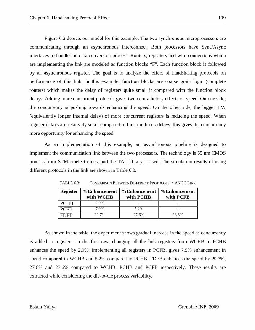
Chapter 6. Handshaking Protocol Effect 109
Eslam Yahya Grenoble INP, 2009
Figure 6.2 depicts our model for this example. The two synchronous microprocessors are
communicating through an asynchronous interconnect. Both processors have Sync/Async
interfaces to handle the data conversion process. Routers, repeaters and wire connections which
are implementing the link are modeled as function blocks “F”. Each function block is followed
by an asynchronous register. The goal is to analyze the effect of handshaking protocols on
performance of this link. In this example, function blocks are coarse grain logic (complete
routers) which makes the delay of registers quite small if compared with the function block
delays. Adding more concurrent protocols gives two contradictory effects on speed. On one side,
the concurrency is pushing towards enhancing the speed. On the other side, the bigger HW
(equivalently longer internal delay) of more concurrent registers is reducing the speed. When
register delays are relatively small compared to function block delays, this gives the concurrency
more opportunity for enhancing the speed.
As an implementation of this example, an asynchronous pipeline is designed to
implement the communication link between the two processors. The technology is 65 nm CMOS
process from STMicroelectronics, and the TAL library is used. The simulation results of using
different protocols in the link are shown in Table 6.3.
TABLE 6.3: COMPARISON BETWEEN DIFFERENT PROTOCOLS IN ANOC LINK
Register %Enhancement with WCHB
%Enhancement with PCHB
%Enhancement with PCFB
PCHB 2.9% - - PCFB 7.9% 5.2% - FDFB 29.7% 27.6% 23.6%
As shown in the table, the experiment shows gradual increase in the speed as concurrency
is added to registers. In the first raw, changing all the link registers from WCHB to PCHB
enhances the speed by 2.9%. Implementing all registers in PCFB, gives 7.9% enhancement in
speed compared to WCHB and 5.2% compared to PCHB. FDFB enhances the speed by 29.7%,
27.6% and 23.6% compared to WCHB, PCHB and PCFB respectively. These results are
extracted while considering the die-to-die process variability.

Chapter 6. Handshaking Protocol Effect 110
Eslam Yahya Grenoble INP, 2009
This circuit example shows how handshaking protocols could be efficiently used to
enhance the speed. One should consider the area and power overhead for using more concurrent
protocols. This overhead is minimized in case of coarse grain pipelines.
Example3: asynchronous rings are nice examples for fine grain pipelines. Asynchronous
rings are composed of cascaded registers which are connected as a ring (last register is connected
to the first one). Consequently internal register delays are the main contributors to the ring total
delay. In this case it is expected that rings which are using more concurrent protocols have more
delay (lower oscillating frequency). More concurrent registers are adding overhead without any
promise for gaining from concurrency. For realizing these results, two asynchronous rings are
designed using 65nm CMOS process from STMicroelectronics. One of these rings is using
WCHB protocol and the other is implemented using PCHB. The WCHB ring is oscillating on 2.8
GHz while the PCHB ring is oscillating on 2.3GHz. As expected, more concurrent protocols have
no interest from the speed point of view in such a context.
These three examples show the following results:
1) Obviously, the speed of asynchronous circuits is affected by the used handshaking
protocol.
2) More concurrent protocols are promising in coarse grain pipelines. In the contrary,
using them in very fine grain pipelines is not efficient from the speed point of view.
3) Mixing handshaking protocols in asynchronous gives the optimum solutions for
speed, power consumption and hardware size.
6.4 Protocol Effect on Power Consumption Distribution.
In many applications where asynchronous logic is applied, the EMI is an important
property. Examples of these applications can be secure chips, synchronizers and ANOC in GALS
(Globally Asynchronous Locally Synchronous) systems. As a result, in the comparison between
different handshaking protocols, we performed a study of the effect of different protocols on the
time-distribution of the circuit activity. Different handshaking protocols give different
concurrency. As a result, event (Evaluation & Reset) time-distribution is affected by the used

Chapter 6. Handshaking Protocol Effect 111
Eslam Yahya Grenoble INP, 2009
protocol. Each event is equivalent to a current consumption in the circuit. This means that the
event distribution is a map to the current distribution. Consequently, studying the effect of the
handshaking protocol on the event distribution in time (equivalently current distribution) gives an
idea about the effect of the protocol on the EMI characteristics. Figure 6.3, 6.4, 6.5 and 6.6 show
the event distribution of an asynchronous pipeline using WCHB, PCHB, PCFB and FDFB
respectively.
From the time distribution in the figures, we can show that the more concurrency in the
protocol the less impulses in the current time-distribution and the higher switching frequency in
the circuit. This conclusion brings up two contradictory factors to optimize. Let us compare
between WCHB and FDFB as they are the two extremes. In WCHB the switching frequency is
lower however there are very high current peaks. On the contrary, FDFB has higher switching
frequency but lower current peaks. This means that the more concurrent protocol is smoothing
the current-consumption peaks in the trade of higher switching frequency. Using this conclusion,
designers can optimize their circuits in terms of power consumption distribution. By defining the
frequency domain of interest, designer can safely trade current peaks to switching frequency.

Chapter 6. Handshaking Protocol Effect 112
Eslam Yahya Grenoble INP, 2009
0 0.5 1 1.5 2 2.5
x 105
0
2
4
6
8
10
12
Time Axis
Even
t
My Draw
Figure 6.3: Time Distribution for WCHB Activity
0 0.5 1 1.5 2 2.5
x 105
0
2
4
6
8
10
12
Time Axis
Even
t
My Draw
Figure 6.4: Time Distribution for PCHB Activity

Chapter 6. Handshaking Protocol Effect 113
Eslam Yahya Grenoble INP, 2009
0 0.5 1 1.5 2 2.5
x 105
0
2
4
6
8
10
12
Time Axis
Even
t
My Draw
Figure 6.5: Time Distribution for PCFB Activity
0 0.5 1 1.5 2 2.5
x 105
0
2
4
6
8
10
12
Time Axis
Even
t
My Draw
Figure 6.6: Time Distribution for FDFB Activity

Chapter 6. Handshaking Protocol Effect 114
Eslam Yahya Grenoble INP, 2009
6.5 Protocol Effect on Process Variability.
Process variability causes deviations in the final circuit throughput. If the technology
supposes a statistical distribution for the gate delays, the circuit composed of these gates would
have statistical performance too. The more concurrency the circuit has the better chance for
averaging different delays. As a result, circuits which are based on more concurrent handshaking
protocols are expected to have less deviation from the average thorough. Concurrency is expected
to minimize the effect of process variability on the final circuit throughput.
For studying the relation between handshaking protocols and process variability effects,
two examples are considered in this sub-section. The first one is for the ANOC link where
different handshaking protocols are used and process variability effect on the final link speed is
recorded. The second example is an asynchronous ring where WCHB stages are replaced by
PCHB stages.
ANOC Link: Asynchronous registers in the link are changed from WCHB to PCHB,
PCFB and FDFB. The statistical distribution for the link throughput is recorded and the
enhancement in the standard deviation of the output is recorded; WCHB case is taken as a
reference. Table 6.4 shows the results of this coarse grain circuit.
TABLE 6.4: RELATION BETWEEN HANDSHAKING HROTOCOLS AND PROCESS VARIABILITY EFFECT
Register PCHB PCFB FDFB
Enhancement compared to WCHB 7.3% 12.6% 17.4%
As shown in the table, we can find a significant enhancement in the standard deviation of
the link speed by using more concurrent protocols. For example the standard deviation when
FDFB is used is 17.4% less than the standard deviation in case of WCHB. As the case in speed,
this enhancement comes in the price of more hardware and more power consumption dedicated
for the register implementation.
Asynchronous Ring: we use this example as a fine grain pipeline circuit. It is interested to
see if the more concurrent protocols would succeed enhancing the circuit properties due to
process variability or they would fail as in the case of speed. In this example, WCHB ring is
Chapter 6. Handshaking Protocol Effect 115
Eslam Yahya Grenoble INP, 2009
compared to PCHB ring and the standard deviation of the oscillating frequency is calculated.
When we replaced WCHB ring stages by PCHB ring stages we recorded an enhancement in the
output frequency standard deviation by around 1%. This result is not justifying the reduction in
frequency, extra HW and extra power consumption caused by PCHB ring stages. Consequently,
using more concurrent handshaking protocols in very fine grain pipelines is not recommended
neither from the speed point of view nor the process variability point of view.
6.6 Conclusion.
In this chapter, the effect of handshaking protocols on speed, power consumption
distribution and effect of process variability is studied. Generally speaking, more concurrent
handshaking protocols would enhance the speed of the asynchronous circuits. However, in very
fine grain pipelines, the extra internal delays of more concurrent protocols would reduce the
speed and consume more power. The final conclusion of our study recommends mixing different
protocols inside the circuit for achieving the optimum compromise between speed, area and
power-consumption.
When events distribution is analyzed for the same circuit which is based on different
handshaking protocols, we noted that WCHB has the higher current impulses and the lower
switching frequency (for the same sequence of events). Adding more concurrency to the circuit,
by using PCHB – PCFB – FDFB, showed a reduction in current impulses and an increase in
switching frequency in the circuit. This study concludes that designers can optimize their circuits
in terms of power consumption distribution. By defining the frequency domain of interest,
designers can trade current peaks to switching frequency.
Finally, more concurrent protocols reduce the effect of process variability on the final
circuit throughput. This result is more applied to coarse grain pipelined circuits. Fine grain
pipelines may not benefit from more concurrent protocols, so adding concurrency in this case is
not recommended from any point of view.

Chapter 6. Handshaking Protocol Effect 116
Eslam Yahya Grenoble INP, 2009
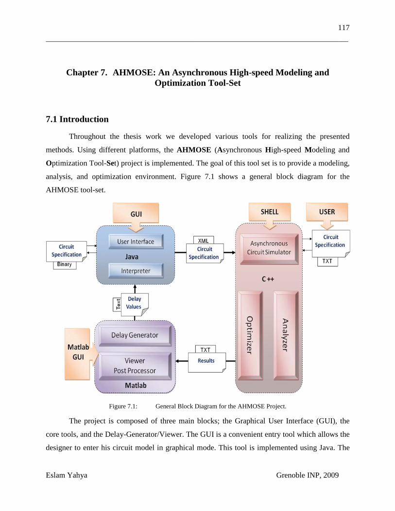
117
Eslam Yahya Grenoble INP, 2009
Chapter 7. AHMOSE: An Asynchronous High-speed Modeling and Optimization Tool-Set
7.1 Introduction
Throughout the thesis work we developed various tools for realizing the presented
methods. Using different platforms, the AHMOSE (Asynchronous High-speed Modeling and
Optimization Tool-Set) project is implemented. The goal of this tool set is to provide a modeling,
analysis, and optimization environment. Figure 7.1 shows a general block diagram for the
AHMOSE tool-set.
Figure 7.1: General Block Diagram for the AHMOSE Project.
The project is composed of three main blocks; the Graphical User Interface (GUI), the
core tools, and the Delay-Generator/Viewer. The GUI is a convenient entry tool which allows the
designer to enter his circuit model in graphical mode. This tool is implemented using Java. The

Chapter7. AHMOSE: An Asynchronous High-speed Modeling and Optimization Tool-Set 118
Eslam Yahya Grenoble INP, 2009
function of this tool is to capture the graphical circuit-model and transform it into a proper format
which is passed to the core tools. The GUI transforms the circuit structure into two file formats;
binary files for storing/loading graphical circuit-structure and XML files for passing the circuit
structures to the core tools.
The core tools are the main part of the project. They are implementing the Asynchronous
circuit simulator, the analyzers, and the optimizer which are introduced in Chapters 3, 4 and 5.
These tools are implemented using C++ programming language. They accept two input formats,
XML file format and Text file format; both formats are human-readable. Results of these tools
are stored in text format. These results could be directly viewed by human eye; however this is
not so efficient especially for statistical outputs.
The third module is responsible for generating the statistical delay values using Matlab
functions. In addition, this module provides to the user visual tools for graphing and statistically
analyze the output results.
7.2 Graphical User Interface “GUI”
During my PhD I had co-supervised the training period (three moth) of two master
students “INP Grenoble TELECOM
The GUI is designed to provide the basic structures which are necessary for modeling
asynchronous circuits. These structures appear in Figure 2.3 in Chapter 2 and they are shown
again in Figure 7.2 for the reader convenience. In addition to the basic structures which are
discussed in Chapter 2, the GUI supports two other structures; the “Control” component and the
“Generic” component. The Control component is used to model the environment which is
providing the control input to Split and Merge (or any other controlled components). By means of
these component, we model the control sequences (which In/Out channel is selected) and the
control delays. Asynchronous circuits could contain some other structures, for instance, a multi-
input multi-output NOC router. This component could not be simply modeled using the basic
”. I would like to thank them for their appreciated help in
developing the GUI especially in writing the related Java code.

Chapter7. AHMOSE: An Asynchronous High-speed Modeling and Optimization Tool-Set 119
Eslam Yahya Grenoble INP, 2009
structures. As a result, we designed a Generic component which is reconfigurable by the user.
The numbers of input, output and control channels are defined by the user. For example, if the
user set this component to have three input channels, one output channel and one control; this
component model a three input Merge. If the Generic component is configured to have four input
channels, four output channels and one control; this could model 4x4 crossbar switch. Designer
should be sure that the new modeled component is supported by the analytical models library
(more details are discussed in the next section). Generic component adds flexibility and
efficiency to our tool set.
Figure 7.2: Basic Structures Suported by the GUI

Chapter7. AHMOSE: An Asynchronous High-speed Modeling and Optimization Tool-Set 120
Eslam Yahya Grenoble INP, 2009
As shown in Figure 7.1, the GUI deals with two kinds of files: files to store the graphical
representation of the circuit and files to provide serialized version of the circuit. Since the GUI is
implemented using Java, we made a study to choose the best file representation. In this study we
compared between XML, Text and Binary file formats; Table 7.1 shows the results of the
comparison. This study is done over ten circuits which are quite large.
TABLE 7.1: COMPARISON BETWEEN GUI FILE FORMATS
File Format
Execution Time Size Readability Serialization Complexity
Portability Java <=> C++ Write Read
XML 1478ms 10004ms 26.2 Mb Yes Easy Yes
Text 628 ms 237 ms 4.2 Mb Yes Hard Yes
Binary 46 ms 67 ms 3.1 Mb No Easy No
The study shows that binary format is optimum for storing the graphical representation of
the circuit; it is fast and small size. Reading these files by human eye is not expected, hence, we
do not care for their readability. Files which are used to store the serialization of the circuit
graphs should be readable and portable between Java and C++. Using Text format is good from
the size and time points of view. However, serialization of the circuit would be complex in this
case. For simplifying the GUI implementation, we choose to serialize the circuit into XML
format. When the circuit is edited and been asked to be re-serialized this process is requested by
human. Therefore, the quite slow response of the XML file is not expected to reduce the tool
performance.
The next step is to design the layout of the GUI; this is shown in Figure 7.3. the layout
consists of:
1. Classical menu bar in which we can find save/load project, launch verification, simulation etc…
2. Design window in which the user can create, delete and connect components.
3. Component bar contains all supported structures.

Chapter7. AHMOSE: An Asynchronous High-speed Modeling and Optimization Tool-Set 121
Eslam Yahya Grenoble INP, 2009
4. Component properties window which displays the properties of the selected
component. In this window, the user can modify the component properties.
5. Status window which provides the user information about the current running
modules, reading/writing files etc...
A snapshot of the implemented GUI appears in Figure 7.4. This GUI was very helpful
during the thesis for building, configuring and modifying the test circuits.
Figure 7.3: Layout of the GUI

Chapter7. AHMOSE: An Asynchronous High-speed Modeling and Optimization Tool-Set 122
Eslam Yahya Grenoble INP, 2009
Figure 7.4: A sanpshot of the GUI
7.3 The Core Tools
The Core tools are the main part of the project. They are implementing the methods which
are proposed throughout the thesis. The Core tools are composed of three main modules; the
Asynchronous Circuit Simulator “ACS”, the Performance Analyzer “PA” and the Performance
Optimizer “PO”.

Chapter7. AHMOSE: An Asynchronous High-speed Modeling and Optimization Tool-Set 123
Eslam Yahya Grenoble INP, 2009
7.3.1 Asynchrones Circuit Simulator
The Asynchronous Circuit Simulator (ACS) is the module which is responsible for
parsing the input files and construct the circuit structure into the memory; Figure 7.5. The ASC
accepts two file formats, XML or Text Format. A parser module reads the input file and
constructs the circuit in the memory. The circuit simulator module solves the circuit and outs the
absolute time information for the different components. These information are passed to the
analyzer and the optimizer. The algorithm of the ASC is depicted in Figure 7.6.
Figure 7.5: Block Diagram of The Asynchronous Circuit Simulator

Chapter7. AHMOSE: An Asynchronous High-speed Modeling and Optimization Tool-Set 124
Eslam Yahya Grenoble INP, 2009
Figure 7.6: Flowchart of The Asynchronous Circuit Simulator
The ACS could be directly launched through a command shell or through the
“Simulation” window in the GUI. Depending on the file format, the ACS selects either XML
parser or Text parser. The parser analyzes the input file and builds the circuit structure into the
memory. After that, the ACS handles the circuit initialization. The components - which are
initialized - affect the status of the preceding and following components. For example, if a
register is initialized by a token then its output request and its input acknowledge have to be
activated. Activating these signals affect some flags in the preceding and following registers. In
the same step, the ACS builds what we call “Solving List (SL)”. This list contains the registers
which are ready to be solved. In other words, registers which have proper input status to store
Evaluation or Reset token. Registers in Solving List “SL” are solved one by one. When a register
is solved the proper signals (Acknowledge/Request) are propagated to the attached registers.

Chapter7. AHMOSE: An Asynchronous High-speed Modeling and Optimization Tool-Set 125
Eslam Yahya Grenoble INP, 2009
These attached registers are tested; if they are ready to be solved they are inserted into the
Solving List etc... The appropriate TTVs (Time Token Vectors) are updated to store the solution
step results. After consuming all the input tokens or solving for the requested simulation time, the
ACS passes the “TTVs” to the Analyzer and/or optimizer. There are cases in which the ACS is
launched by the optimizer. In these cases, the circuit structure is modified by the optimizer and is
requested to be re-analyzed.
7.3.2 Performance Analyzers
The connection between the Timing Analyzer “TA” and the ACS appears in Figure 4.5.
The connection between the Power Analyzer “PA” and the ACS appears in Figure 4.10. The
ACS passes the TTVs to the Analyzers. The requested analysis Timing/Power is passed to the
corresponding analyzer. Using the “Timing-Metrics Equations” library for the Timing Analyzer
and the “Event to Power” library for the Power Analyzer, the requested analysis is done and
passed to the user by displaying on the command shell or by writing into output files.
Figure 7.7: Flowchart of The Performance Anlyzers
Figure 7.7 depicts the algorithm used in the analyzers. The analysis requests come from
the command shell. Based on the analysis type (timing or power), the analyzer uses the

Chapter7. AHMOSE: An Asynchronous High-speed Modeling and Optimization Tool-Set 126
Eslam Yahya Grenoble INP, 2009
corresponding module. After calculating the requested metrics, the analyzer calls the optimizer (if
the user requests optimization for the results) or writes the output files.
7.3.3 Performance Optimizer
If the user asks for optimizing the circuit, the timing analyzer calls the Optimizer.
Connection between ACS, Analyzer and Optimizer is shown in Figure 5.1. Optimizer applies the
optimization algorithms discussed in Chapter 5. After that, it checks if there are some possible
optimization for the circuit structure or not. If yes, the optimizer modifies the circuit structure in
the memory and calls the Asynchronous Circuit Simulator “ACS”. The ACS solves the new
circuit structure and passes the results to the analyzer. The timing analyzer determines the
concerned metrics and passes results to the optimizer which decides for the next step etc... Figure
7.8 shows the algorithm of the optimizer.
Figure 7.8: Flowchart of The Performance Anlyzers
All the core tools are implemented using C++. Object oriented programming paradigms
guarantee nicely organized implementation and the easily extension of the tools. For example,
when we added the generic component, it is needed to add the analytical model of this component

Chapter7. AHMOSE: An Asynchronous High-speed Modeling and Optimization Tool-Set 127
Eslam Yahya Grenoble INP, 2009
to the library and to extend the solving methods to cover the different structures such as crossbar
switches or network routers. Implementing analytical models in a separate library makes the
extension of the tools straightforward. Figure 7.9 shows some snapshots of the shell interface of
the tools.
Figure 7.9: Snapshots from the Core Tools Shell
7.4 Delay Generator / Viewer and Post Processing
All the Monte Carlo analysis show that the manufacturer models of the delay variability
uses Normal distributions. There are several methods to generate normal distributions; the most
Chapter7. AHMOSE: An Asynchronous High-speed Modeling and Optimization Tool-Set 128
Eslam Yahya Grenoble INP, 2009
basic is to invert the standard normal Cumulative Distribution Function “cdf”. More efficient
methods are also known such as the Box-Muller transform. An even faster algorithm is the
ziggurat algorithm. Matlab provides functions for generating different statistical distributions
especially Gaussian. Delay generator is implemented using these functions.
Moreover, Matlab provides efficient statistical tools which are able to process the
statistical output of our tools and give important information as standard deviation of the output.
For their efficiency and simplicity, Matlab functions are used to implement the viewer and post
processor tools. However, using Matlab gives two disadvantages to the flow. First, calling these
Matlab functions consumes nontrivial memory space even though the functions themselves are
quite simple. Second, the user of the current version of AHMOSE tools needs to have Matlab for
generating the Delay Token Vector “DTVs”. There are alternative solutions. For instance, the
GNU scientific library provides some modules for generating Gaussian distributions. Using these
functions could enhance the efficiency of our tools; however, this needs more investigation.
7.5 Conclusion
Various methods have been developed during the PhD work. An implementation of these
methods was needed for validation. Complete project is planned for implementing the tool flow.
Java is used for implementing a graphical user interface “GUI” which provides to the user an
efficient entry tool. Developed methods have been implemented using C++ in the three main
software modules. These modules are interacting to simulate, analyze and optimize the circuits.
The results are viewed and post processed using Matlab. While designing these tools, we have
taken into consideration the extension of their features. That makes straightforward the inclusion
of new components, new structures and new protocols. An evaluation version of the AHMOSE
tools is available on the internet. They can be downloaded and installed on Windows OS.
Many extensions of the current implementations are possible for enhancing the tools
features and the efficiency of their performance. Including the GNU library for the delay
generator, using some C++ modules for the viewer, enriching the analytical models library and
enhancing the GUI quality are examples of the potential enhancement.

129
Eslam Yahya Grenoble INP, 2009
Chapter 8. Conclusion and Prospective
Asynchronous circuits are promising solution for many problems in recent technologies.
Design, analysis and optimization of asynchronous circuits are interesting topics for research and
development. Especially timing analysis and optimization need the development of new methods
and tools.
In this thesis, we investigated the behavior of asynchronous circuits in the presence of
delay variability. Based on a structural view, a modeling method for asynchronous circuits is
developed. This modeling method uses asynchronous registers as barriers for dividing the circuit
into separate islands. By means of analytical model for the handshaking between these islands,
the total circuit performance is analyzed. Based on this analysis, an optimization method is
presented. This method optimizes the number of asynchronous registers inserted inside the circuit
to achieve optimal hardware utilization. Throughout the work, we noticed an important impact of
the used handshaking protocol on speed, power consumption distribution and effect of delay
variability. This impact is investigated and some guidelines are presented. Finally, a complete
tool flow is developed for validating the presented methods.
Handshaking protocols are important milestone in the proposed method. Consequently,
we started by defining some behavioral metrics of different handshaking protocols. As an
illustrative example, the handshaking protocols from Caltech are analyzed based on these
metrics. A proposition for a new handshaking protocol is introduced and the QDI circuit
implementation of this protocol is shown.
A class of time-marked graphs is used to develop analytical models for different
handshaking protocols. By means of these analytical models, a complete modeling method has
been developed. This method is a mixture between closed form equations and iterative simulation
solutions. Compared to previous works, our model avoids modeling the whole circuit as a single
problem. This is done by considering asynchronous registers as barriers which are partitioning
the circuit. In this modeling method, nondeterministic structures are efficiently supported. No
restrictions on the circuit structures are needed for a correct behavior of our model. The method

Chapter 8. Conclusion and Prospective 130
Eslam Yahya Grenoble INP, 2009
fully supports delay variability by means of a simple and flexible delay model. For validating our
method, a complete event-driven circuit simulator has been developed. This simulator provides a
convenient GUI and a netlist like entry environment to the user. A complete analytical-models
library of different handshaking protocols has also been implemented. The circuit simulator is
using a nice and efficient delay generator which is devoted for the inclusion of the delay
variability. The simulator analyzes the circuits and produces the output Time Token Vectors
“TTVs” which are very useful information to extract many interesting performance metrics.
Based on the produced “TTVs”, a method for analyzing the time performance of
asynchronous circuits is proposed. Our methods and tools show flexibility with different circuit
structures, mixing handshaking protocols in a single circuit and using different delay types. One
of the important advantages of the proposed method is the linear growth of its complexity with
respect to the circuit size. Afterward, a method for converting the circuit events into
current/power consumption information is used. By means of this method, we built a power
analyzer which is able to estimate the power consumption and its distribution in time. In addition
to this, the methods could analyze “Within Die” and “Die To Die” process variation with a very
high accuracy.
Subsequently, the problem of optimizing deterministic asynchronous pipelines by
controlling the number of registers is addressed. The target is to find the minimum number of
registers which satisfy the given performance constraints. Moreover, the method finds the
optimum placing of these registers which not only satisfies the target performance, but also
results in the maximum achievable performance using this number of registers. To accomplish
these targets, an optimal algorithm is analyzed and implemented. The condition guaranteeing that
adding registers to the pipeline is monotonically decreasing the cycle time is stated and proven.
Two possible optimizations are addressed and by using “Branch and Bound”, different heuristics
are applied. The optimality of the solution after applying these optimizations is proven.
The impact of the handshaking protocol on different performance metrics is discussed.
Generally speaking, more concurrent handshaking protocols would enhance the speed of the
asynchronous circuits. However, in very fine grain pipelines, the extra internal delays of more
concurrent protocols would reduce the speed and consume more power. The final conclusion of
Chapter 8. Conclusion and Prospective 131
Eslam Yahya Grenoble INP, 2009
our study recommends mixing different protocols inside the circuit for achieving the optimum
compromise between speed, area and power-consumption. We produced different versions of a
same circuit; each version is based on a different handshaking protocol. When event distribution
is analyzed for these versions, we noted that WCHB has the higher current impulses and the
lower switching frequency. Adding more concurrency to the circuit, by using PCHB – PCFB –
FDFB, shows a reduction in current impulses and an increase in switching frequency. This study
concludes that designers can optimize their circuits in terms of power consumption distribution.
By defining the frequency domain of interest, designer can trade current peaks to switching
frequency. Finally, more concurrent protocols reduce the process variability effects on the final
circuit throughput. This result is more applicable to coarse grain pipelined circuits.
Finally, a software platform is implemented to provide a complete flow for our methods.
A flexible GUI has been developed using Java. Matlab codes are used for producing delay PDFs
and final output viewers. By means of some interpreters, the graphical circuit structures and the
delay PDFs are used to produce a netlist circuit specification file. This file is used as an entry to
the event driven circuit simulator which is implemented in C++. Based on this simulator, timing
analyzer and power analyzer are implemented. On top of that, we added another application
which implements the proposed optimization algorithms. By using Matlab, some viewers and
post-processing functions are also implemented.
There are many possible extensions to this work such as hardware implementation of
different handshaking protocols of nonlinear elements. There are many investigations on how to
distribute and collect acknowledgment signals in nonlinear elements. The presented modeling
method provides the background for building an architecture analyzer. This analyzer would be
devoted for detecting the probability of having deadlocks in the circuit structures. Some
extensions to the presented optimization methods are possible too. Using “waiting times” is
probably a very efficient way to optimize asynchronous circuits. In addition, the presented
optimizations are extendable to cover non-deterministic pipelines. We already worked on that,
however, this point needs more investigations. The implemented tools have many possible
extensions too. They can be enhanced by including efficient modules and APIs which are
available.

Chapter 8. Conclusion and Prospective 132
Eslam Yahya Grenoble INP, 2009

133
Eslam Yahya Grenoble INP, 2009
[1] T. Agerwala. Putting Petri nets to work. IEEE Computer, 12(12):85–94, December 1979.
References
[2] Al Davis, Steven M. Nowick: An Introduction to Asynchronous Circuit Design, UUCS-97-013, (1997)
[3] Andrew Lines: Pipelined Asynchronous Circuits. Master Thesis (1995)
[4] A. Ashkinazy, D. Edwards, C. Farnsworth, G. Gendel, and S. Sikand. Tools for validating asynchronous digital circuits. In Proceedings of the International Symposium on Advanced Research in Asynchronous Circuits and Systems (Async94), pages 12-21. IEEE Computer Society Press, November 1994.
[6] Steven M. Burns. Performance Analysis and Optimization of Asynchronous Circuits. PhD thesis, California Institute of Technology, 1991.
[5] Robert Berks and Jo Ebergen. Response time properties of linear pipelines with varying cell delays. In Proc. International Workshop on Timing Issues in the Speciation and Synthesis of Digital Systems (TA U), December 1997.
[7] S. Chakraborty, D.L. Dill, K.-Y. Chang, and K.Y. Yun. Timing analysis for extended burst-mode circuits. In Proceedings of the International Symposium on Advanced Research in Asynchronous Circuits and Systems (Async97). IEEE Computer Society Press, April 1997.
[8] S. Chakraborty and D.L. Dill. More accurate polynomial-time min-max timing simulation. In Proceedings of the International Symposium on Advanced Research in Asynchronous Circuits and Systems (Async97). IEEE Computer Society Press, April 1997.
[9] Supratik Chakraborty, David L. Dill, and Kenneth Y. Yun. Min-max timing analysis and an application to asynchronous circuits. Proceedings of the IEEE, 87(2):332–346, February 1999.
[10] Tiberiu Chelcea, Girish Venkataramani, Seth C. Goldstein: “Area Optimizations for Dual-Rail Circuits Using Relative-Timing Analysis”. In Proceedings of 13th IEEE International Symposium on Asynchronous Circuits and Systems, pages 117-128. California, USA, 2007.
[11] T.-A. Chu. Synthesis of self-timed control circuits from graphs: an example. In Proceedings of the International Conference on Computer Design, pages 565--571, 1986.
[12] T.-A. Chu, “Synthesis of self-timed VLSI circuits from graph-theoretic specifications,” Ph.D. dissertation, MIT, June 1987.
[13] Jo Ebergen. Squaring the FIFO in GasP. In Proc. International Symposium on Advanced Research in Asynchronous Circuits and Systems, pages 194–205. IEEE Computer Society Press, March 2001.
[14] Jo Ebergen and Robert Berks. “Response Time Properties of Some Asynchronous Circuits”. Proceedings of the 3rd International Symposium on Advanced Research in Asynchronous Circuits and Systems, Eindhoven, Netherlands, 1997.
[15] J. C. Ebergen, S. Fairbanks and I. E. Sutherland, “Predicting performance of micropipelines using Charlie diagrams”, ASYNC’98, San Diego, CA, USA, IEEE, April 1998, pp. 238 - 246.
[16] Jo Ebergen and Robert Berks. Response time properties of linear asynchronous pipelines. Proceedings of the IEEE, 87(2):308-318, February 1999.
[17] S. Fairbanks and S. Moore, “Analog micropipeline rings for high precision timing”, ASYNC’04, CRETE, Greece, IEEE, April 2004, pp. 41–50.
[18] O. Garnica, J. Lanchares, R. Hermida, “Optimization of asynchronous delay-insensitive pipeline latency using stage reorganization and optimal stage parameter estimation” Proceedings of the International Conference on Application of Concurrency to System Design (ACSD), Newcastle upon Tyne, UK, pp. 167-178, 2001.
[19] H. Hulgaard, S.M. Burns, T. Amon, and G. Borriello. Practical applications of an efficient time separation of events algorithm. In Proceedings of the IEEE/ACM International Conference on Computer-Aided Design, pages 146-151. IEEE Computer Society Press, November 1993.
[20] H. Hulgaard and S.M. Burns. Bounded delay timing analysis of a class of CSP programs with choice. In Proceedings of the International Symposium on Advanced Research in Asynchronous Circuits and Systems (Async94), pages 2-11. IEEE Computer Society Press, November 1994.
[21] H. Hulgaard, S. M. Burns, T. Amon, and G. Borriello. An algorithm for exact bounds on the time separation of events in concurrent systems. IEEE Transactions on Computers, 44(11):1306–1317, November 1995.

References 134
Eslam Yahya Grenoble INP, 2009
[22] Henrik Hulgaard. Timing Analysis and Verification of Timed Asynchronous Circuits. PhD thesis, Department of Computer Science, University of Washington, 1995.
[23] Jacques J.A., Simon Moore, Huiyun Li, Robert Mullins, George Taylor: Security Evaluation of Asynchronous Circuits. CHES, pp. 137-151 (2003)
[24] Jens SparsØ, Steve Furber: Principles of Asynchronous Circuit Design. A System Perspective. Kluwer Academic Publishers (2001)
[25] Jens Sparsø and Jørgen Staunstrup. Delay-insensitive multi-ring structures. The VLSI journal, 15(3):313–340, October 1993.
[26] Sangyun Kim and Peter Beerel: Pipeline Optimization for Asynchronous Circuits: Complexity Analysis and an Efficient Optimal Algorithm. IEEE Transactions of Integrated Circuit and Systems , VOL. 25, NO. 3, 2006
[27] Benoit Lasbouygues, Robin Wilson, Member, IEEE, Nadine Azémard, and Philippe Maurine: “Temperature- and Voltage-Aware Timing Analysis”. IEEE TRANSACTIONS ON COMPUTER-AIDED DESIGN OF INTEGRATED CIRCUITS AND SYSTEMS, VOL. 26, NO. 4, APRIL 2007.
[28] Benoit Lasbouygues, Robin Wilson, Member, IEEE, Nadine Azémard, and Philippe Maurine: “Temperature and Voltage Aware Timing Analysis: Application to Voltage Drops”. In proceedings of DATE 07.
[29] Luciano Lavagno, Kurt Keutzer, Alberto L. Sangiovanni-Vincentelli, “Synthesis of Hazard-Free Asynchronous Circuits with Bounded Wire Delays”, IEEE TRANSACTIONS ON COMPUTER-AIDED DESIGN OF INTEGRATED CIRCUITS AND SYSTEMS, VOL. 14, NO. 1, JANUARY 1995.
[30] Marc Renaudin, Joao Leonardo: Asynchronous Circuits Design: An Architectural Approach. (2003)
[31] A. J. Martin, A. Lines, R. Manohar, M. Nystroem, P. Penzes, R. Southworth, and U. Cummings, “The design of an asynchronous MIPS R3000 microprocessor” in Proc. Conf. Advanced Research VLSI, Ann Arbor, MI, Sep. 1997, pp. 164–181.
[32] V. Migairou, R. Wilson, S. Engels, Z. Wu, N. Azemard, and P. Maurine. “A Simple Statistical Timing Analysis Flow and Its Application to Timing Margin Evaluation”. PATMOS 2007, LNCS 4644, pp. 138–147.
[33] T. Murata. Petri Nets: Properties, Analysis and Applications. Proceedings of the IEEE, 77(4):541–580, April 1989.
[34] Chris J. Myers and Teresa H.-Y. Meng. Synthesis of timed asynchronous circuits. IEEE Transactions on VLSI Systems, 1(2):106–119, June 1993.
[35] Peggy McGee, Steven Nowick, E.G. Coffman: Efficient performance analysis of asynchronous systems based on periodicity. 3rd IEEE / ACM / IFIP CODE (2005)
[36] Peggy McGee, Steven Nowick: “An efficient algorithm for time separation of events in concurrent systems”. ”. In Proceedings of IEEE/ACM International Conference on Computer-Aided Design pp180-187. ICCAD 2007.
[37] Peter A. Beerel: Asynchronous Circuits: An Increasingly Practical Design Solution. Proceedings of ISQED’02, IEEE Computer Society (2002)
[38] C. V. Ramamoorthy and G. S. Ho. Performance evaluation of asynchronous concurrent systems using Petri nets. IEEE Transactions on Software Engineering, 6(5):440–449, September 1980.
[39] L. Y. Rosenblum and A. V. Yakovlev, “Signal graphs: From self-timed to timed ones,” in Int. Workshop. Timed Petri Nets, Torino, Italy, 1985.
[40] Sachin Sapatnekar: “Timing”. Kluwer Academic Publishers, ISBN 1-4020-7671-1, 2004.
[41] A. Semenov and A. Yakovlev. Verification of asynchronous circuits using time Petri net unfolding. In 33rd ACM/IEEE Design Automation Conference, June 1996.
[42] Stephen. B. Furber and Paul Day: Four-Phase Micropipline Latch Control Circuits. IEEE Transitions on VLSI Systems, 4(2):247-253, (1996)
[43] Ted Williams: Latency and Throughput Tradeoffs in Self-Timed Speed-Independent Pipelines and Rings. Technical Report No. CSL-TR-90-431 (1990).
[44] T. E. Williams, “Self-timed rings and their application to division,” Ph.D. thesis, Dept. Elect. Eng. Comput. Sci., Stanford Univ., CA, Jun. 1991.

References 135
Eslam Yahya Grenoble INP, 2009
[45] Ted Williams: Performance of Iterative Computation in Self-Timed Rings. Journal of VLSI Signal Processing, 7, 17-31 (1994).
[46] C.H. (KEES) Van Berkel, Mark B. Josephs, Steven M. Nowick: Scanning the Technology. Applications of Asynchronous Circuits. Proceedings of the IEEE, Vol. 87, No 2 (1999)
[47] E. Verlind, G. de Jong, and B. Lin. Efficient partial enumeration for timing analysis of asynchronous systems. In 33rd ACM/IEEE Design Automation Conference, June 1996.
[48] A. Winstanley and M. R. Greenstreet, “Temporal properties of self timed rings”, CHARM’01, London, UK, Springer-Verlag, April 2001, pp. 140 - 154.
[49] A. J. Winstanley, A. Garivier, and M. R. Greenstreet, “An event spacing experiment,” Proceedings of the Eighth International Symposium on Asynchronous Circuits and Systems, ASYNC’02, pp. 47–56, Apr. 2002.
[50] Aiguo Xie and Peter A. Beerel. Symbolic techniques for performance analysis of timed systems based on average time separation of events. In Proc. International Symposium on Advanced Research in Asynchronous Circuits and Systems, pages 64–75. IEEE Computer Society Press, April 1997.
[51] Aiguo Xie, Sangyun Kim, and Peter A. Beerel. Bounding average time separations of events in stochastic timed Petri nets with choice. In Proc. International Symposium on Advanced Research in Asynchronous Circuits and Systems, pages 94–107, April 1999.
[52] A. Yakovlev and A. M. Koelmans. Petri nets and digital hardware design. In Lectures on Petri nets II: Basic Models, Lecture Notes in Computer Science. Springer-Verlag, 1998.
[53] V. Zebilis and C. P. Sotiriou, “Controlling event spacing in self-timed rings”, ASYNC’05, New York, USA, IEEE, March 2005, pp. 109 - 115.

References 136
Eslam Yahya Grenoble INP, 2009
[54] Eslam Yahya, Oussama Elissati, Hatem Zakaria, Laurent Fesquet and Marc Renaudin : " Programmable/Stoppable Oscillator Based on Self-Timed Rings", IEEE ASYNC’2009, May 17-20, 2009, UNC Chapel Hill, USA.
Publications produced during the thesis:
[55] Eslam Yahya and Laurent Fesquet, “Asynchronous Design: A Promising Paradigm for Electronic Circuits and Systems“to be published IEEE ICECS’2009, 13th-16th December 2009, Hammamet, Tunisie.
[56] Oussama Elissati, Eslam Yahya, Laurent Fesquet and Sébastien Rieubon, “Oscillation Period and Power Consumption in Configurable Self-Timed Ring Oscillators” IEEE NEWCAS-TIASA’2009, Jun 28–July 1st, 2009, Toulouse, France.
[57] Eslam Yahya, Laurent Fesquet and Marc Renaudin : " Asynchronous High-speed Modeling and Optimization tool Set (AHMOSE)", DATE 2009 (University Booth), Nice, France, April 2009.
[58] Eslam Yahya, Marc Renaudin and Gregory Lopin: "Standard-Logic Quasi Delay Insensitive Registers”. VLSI-SOC'08, Rhodes Island, Greece, pp: 465- 468, 2008
[59] Eslam Yahya and Marc Renaudin: "Optimal Asynchronous Linear-Pipelines". PRIME'08, Istanbul, Turkey, pp 9-12, 2008. (Best Paper Award: Silver Leaf)
[60] Eslam Yahya and Marc Renaudin: "Asynchronous Linear Pipelines: An efficient-Optimal pipelining Algorithm". ICECS'08, Malta, 2008
[61] Eslam Yahya and Marc Renaudin: " AHMOSE: Towards a Circuit Level Solution for Process Variability". Workshop on Impact of Process Variability on Design and Test, Held at DATE'08, Munich, Germany, 2008
[62] Eslam Yahya and Marc Renaudin: "Asynchronous Linear-Pipeline with Time Variable Delays: Performance Modeling, Analysis and Slack Optimization”. DCIS'08, Grenoble, France, 2008
[63] Eslam Yahya and Marc Renaudin: "Asynchronous High-speed Modeling and Optimization tool Set (AHMOSE)". Demo in ASYNC'08 Exhibition & Demo Sessions, New-Castle, UK, 2008
[64] Eslam Yahya and Marc Renaudin: "Performance Modeling and Analysis of Asynchronous Linear-Pipeline with Time Variable Delays". ICECS'07, Marrakech, Morocco, pp. 1288-1291, 2007
[65] Eslam Yahya and Marc Renaudin: "Performance Modeling and Analysis of Asynchronous Linear-Pipeline” SOC-SIP 2007, Paris, France, 2007
[66] Eslam Yahya and Marc Renaudin: "QDI Latches Characteristics and Asynchronous Linear Pipeline Performance Analysis” PATMOS 2006, Montpellier, France, pp 583-592, 2006
[67] Eslam Yahya, Marc Renaudin: Asynchronous Buffers Characteristics: Molding and Design. Research Report, TIMA-RR--06/-01--FR 2006
[68] Eslam Yahya, Marc Renaudin and Gregory Lopin: Standard-Logic Quasi Delay Insensitive Latches, TIMA-RR--06/06-04--FR 2006

Modélisation, Analyse et Optimisation des Performances des Circuits Asynchrones Multi-Protocoles
RESUME Les circuits asynchrones suscitent de nombreux intérêts à bien des égards. Cependant la modélisation,
l'analyse et l'optimisation des circuits asynchrones constituent des pierres d'achoppement à la diffusion de cette
technologie sur un plan commercial. Ce travail vise le développement de modèles de circuits asynchrones
capables de retranscrire efficacement les protocoles « poignée de main ». Sur la base de ces modèles, une
technique d’analyse rapide et précise des circuits a été développée. Cette technique offre un support complet
pour l’analyse de délais statistiquement variables et pour différentes structures de circuit (linéaire / non linéaire,
sans / avec condition). Elle permet de réaliser des analyses statiques de timing, de consommation électrique et
des effets des variabilités sur les circuits asynchrones. En sus de ces méthodes de modélisation et d'analyse, une
technique d'optimisation a été développée. Cette technique d'optimisation est basée sur une réduction du nombre
de registres asynchrones à un nombre minimal capable de satisfaire les contraintes de performance. L’utilisation
des méthodes proposées a permis l’étude de différents protocoles asynchrones et de leurs impacts sur la vitesse,
la consommation et la variabilité des procédés de fabrication. Les méthodes proposées ont été validées grâce à
un jeu d'outils logiciels écrits en C + +, Java et Matlab. Ces outils se sont avérés rapides, efficaces et dotés d’une
très bonne précision de calcul.
MOTS-CLES:“Logique asynchrone”, “Modélisation, Analyse et Optimisation des Performances”, “
Pipelines asynchrone non-linéaire ”, “ Variation PVT ”, “ Poignée de main asynchrone”.
Performance Modeling, Analysis and Optimization of Multi-Protocol Asynchronous Circuits
ABSTRACT Asynchronous circuits show potential interest from many aspects. However modeling, analysis
and optimization of asynchronous circuits are stumbling blocks to spread this technology on commercial level.
This thesis concerns the development of asynchronous circuit modeling method which is based on analytical
models for the underlying handshaking protocols. Based on this modeling method, a fast and accurate circuit
analysis method is developed. This analysis provides a full support for statistically variable delays and is able to
analyze different circuit structures (Linear/Nonlinear, Unconditional/Conditional). In addition, it enables the
implementation of timing analysis, power analysis and process-effect analysis for asynchronous circuits. On top
of these modeling and analysis methods, an optimization technique has been developed. This optimization
technique is based on selecting the minimum number of asynchronous registers required for satisfying the
performance constraints. By using the proposed methods, the asynchronous handshaking protocol effect on
speed, power consumption distribution and effect of process variability is studied. For validating the proposed
methods, a group of tools is implemented using C++, Java and Matlab. These tools show high efficiency, high
accuracy and fast time response.
Keywords:“ “Asynchronous Logic”, “Performance Modeling, Analysis and Optimization”, “Nonlinear
Asynchronous Pipelines”, “PVT Variation”, “Asynchronous Handshaking””.
Thèse préparée au laboratoire TIMA (Techniques de l’Informatique et de la Microélectronique pour l’Architecture des ordinateurs), Grenoble INP, 46 avenue Félix Viallet, 38031, Grenoble Cedex 1, France.
ISBN 978-2-84813-147-4