modification of the properties of cadimium selenide thin ... · an-najah national university...
TRANSCRIPT

An-Najah National University
Faculty of Graduate Studies
MODIFICATION OF THE PROPERTIES OF CADIMIUM
SELENIDE THIN FILMS IN PHOTOVOLTAIC
SOLAR CELLS
By:
Huda Solaiman Mohamad Sabri, M.Sc. Physics student
Supervisors:
Dr. Subhi K. Salih, Ph.D.
And
Professor Hikmat S. Hilal, Ph.D.
Submitted in Partial Fulfillment of the Requirements for the Degree of Master of Science in PHYSICS, Faculty of Graduate Studies, at An-Najah National University, Nablus, Palestine.
2009

II
MODIFICATION OF THE PROPERTIES OF CADMIUM SELENIDE THIN FILMS IN PHOTOVOLTAIC
SOLAR CELLS
By:
Huda Solaiman Mohamad Sabri
This thesis was defended successfully on 5/7/2009, and approved by:
Committee Members Signature
1. Dr. Subhi Salih (Supervisor) ...
2. Prof. Hikmat Hilal (Co-Supervisor)
3. Dr. Iyad Saadeddin (Internal Examiner)
4. Dr. Ayman Al Haj Daoud (External Examiner) . ..

III
Biographical Sketch
Huda S. M. Sabri, was born in Qalqelia. In 1981 she graduated from
Qalqelia Secondary School. In 1999 she graduated from An-Najah National
University (Nablus- Palestine) with the degree of Bachelor of Science in
Physics. In 2005 she enrolled in Graduate College at An-Najah National
University, and she had been engaged in research under the supervision of
Professor Hikmat S. Hilal and Dr. Subhi Salih.

IV
Dedication
To my husband .
To my sons .
To everyone who wants to revolute and enrich
his / her knowledge ..

V
Acknowledgements
The author wishes to express her sincere appreciation to her supervisors Dr.
Subhi K. Salih and Professor Hikmat S. Hilal for their guidance, help and
encouragement throughout research work and writing up.
The author would likes to acknowledge the assistance of Dr. Iyad A.
Saadeddin and Mr. Ahed Zyuod (Ph.D. student) of An-Najah National
University.
I wish to express my appreciation to the patience and encouragements
given to me by my husband.
Huda S. Sabri
Nablus-An-Najah N.University

VI
:
MODIFICATION OF THE PROPERTIES OF CADIMIUM
SELENIDE THIN FILMS IN PHOTOVOLTAIC
SOLAR CELLS
.
Declaration
The work provided in this thesis, unless otherwise referenced, is the
researcher's own work, and has not been submitted elsewhere for any other
degree or qualification.
: Student's name:
: Signature:
: Date:

VII
List of Contents
Title
Page
Committee Decision ii
Biographical Sketch iii
Dedication iv
Acknowledgements ..v
List of Contents ...vii
List of Figures .xii
List of Tables xvii
Abstract (in English) .xviii
Chapter one: Introduction .1
1.1 Objectives ..1
1.2 Hypothesis.................................................................................................2
1.3 Previous studies 3
1.4 Energy Band Gap ..5
1.5 Conduction in Semiconductors ..6
1.6 Electron and Hole Current ..7
1.7 The p-n Junction .7
1.8 Formation of the Depletion Region ..8
1.9 Barrier Potential ....9
1.10 Techniques of Light to-Electricity Conversion ..9
i ) Photovoltaic Cells: (PV) .10
ii ) Photoelectrochemical Cell: (PEC) ..12

VIII
a) The Semiconductor Electrolyte Interface 12
b) Principles of PEC Energy Conversion ..13
1.11 Dark Current .15
1.12 Photo Current 16
1.13 Perturbations of the Ideal Model of PEC Systems ..18
i) Corrosion 18
ii) Surface States .19
iii) Doping Instability 21
1.14 Types of Solar Cells 22
a) Mono-Crystalline Electrodes ..22
b) Thin film or Amorphous Electrodes ...22
1.15 Advantages and Disadvantages of PEC Cells .23
1.16 Types of Semiconductor Materials for PEC Cells 23
1.17 Earlier Studies on CdSe .25
1.18 Major Theme of this Study 28
Chapter Two: Experimental Work ...30
2.1 Materials 30
2.1.1 Chemicals and Solvents 30
2.1.2 Preparation and Characterization of MnP ..30
2.1.3 Etching Process 32
2.1.4 Preparation of CdSe Thin Films 33
2.1.5 Annealing Process .35

IX
2.1.6 Cooling Process 35
a) Quenching (Fast Cooling) 35
b) Slow Cooling Process .35
2.2 Equipment .36
2.2.1 Measuring Devices 36
2.2.2 PEC Cell 37
2.2.3 Light Source 38
2.3 PEC Measurements 38
2.3.1 Current Density Potential Plots .38
2.3.2 Stability Testing .39
2.4 UV/Visible Absorption Spectra Measurements . 39
2.5 Photoluminescence (PL) Emission Spectra .40
2.6 Coating the Electrodes with a Polymer ...40
2.7 Measuring the Thickness of CdSe Layer .42
Chapter Three: Results ....43
General Remarks .42
3.1 Enhancement Studies of Uncoated CdSe Film Electrodes .43
3.1.1 UV/Visible Absorption Spectra 44
3.1.2 Photoluminescence Emission Spectra .48
3.1.3 Current Density Potential Plots .50
3.1.4 The Effect of Redox Couple ..52
a) Dark J-V Plots for CdSe Electrodes 52

X
b) Photo J-V Plots for CdSe Electrodes 53
3.2 Effect of Coating CdSe Thin Films with MnP/Polysiloxane 57
a) Dark J-V Plots for CdSe Electrodes with Polymer .58
b) Photo J-V Plots for CdSe Electrodes with Polymer 63
c) Electrode Stability .68
d) Effect of Annealing 69
e) Effect of Rate of Cooling ..69
f) Cell Efficiency Studies ..71
Chapter Four: Discussion ..74
4.1 Introduction .74
4.2 Effect of Annealing and Rate of Cooling on Electronic Absorption ..76
Spectra.
4.3 Effect of Annealing on (PL) Spectra .: ..76
a) Quenched CdSe Samples Prepared at RT .77
b) Slowly Cooled CdSe Samples Prepared at RT .77
4.4 Effect of Coating Thin Films with a Layer of Polymer ..78
4.5 Effect of Annealing on CdSe Film Characteristics ..80
4.5.1 Effect of Annealing on Dark J-V Plots ..80
4.5.2 Effect of Annealing on Photo J-V Plots 81
4.5.3 Effect of Annealing on Film Stability ..82
4.6 Effect of Cooling on CdSe Film PEC Characteristics 82
a) Dark J-V Plots .82
b) Photo J-V Plots 82
c) Film Stability ...83
4.7 Effect of Cooling Rate on Cell Efficiency .83

XI
Conclusions 84
Suggestions for Further Works .85
References 86

XII
List of Figures
Figure No. Title Page
1.1 A schematic showing band structure for: 6
a) insulators, b) semiconductors, c) conductors.
1.2 Depletion layer is the space charge region 8
in pn structure.
1.3 Potential barrier created due to depletion 8
layer formation.
1.4 Solar batteries in series 10
1.5 Storage of solar energy in photo voltaic cell. 11
1.6 Equivalent circuit of ideal solar cell 12
1.7 Energy level diagram for SC-electrolyte junction. 13
1.8 Energy level diagram regenerative cell at: 14
(a) equilibrium and (b) during illumination.
1.9 Dark and photo currents observed in an n-SC/ 15
electrolyte PEC cell.
1.10 Isoenergetic charge transfer of hole from n-type 20
SC to occupied state of electrolyte redox couple.
Redox energy levels have a distribution due to
solvent-ion interactions.
1.11 Mediation of charge transfer by surface state at 21
n-type SC. a) Majority carrier injection through
the barrier produced by band bending.
b) Photo-generated minority carrier injection via
surface state.
1.12 Plot of CdSe crystallite size vs. annealing 25
temperature of CdSe thin films.

XIII
1.13 Variation of CdSe film thickness with deposition time. 26
1.14 SEM of CdSe thin films (a) as-deposited and 27
(b) annealed at 673 K.
2.1 MnP polymer. 31
2.2 The electronic absorption spectra in UV/ visible 31
region for MnP solution in methanol.
2.3 The electronic absorption spectra in the 31
UV/visible region for MnP embedded into
a polysiloxane polymer solid matrix.
2.4 The electronic absorption spectra in the 32
UV/visible region for MnP embedded into
a polysiloxane polymer solid matrix after
annealing at 150
for 30 min. under N2 atmosphere.
2.5 The electronic absorption spectra in the UV/visible 32
region for solid polysiloxane membrane.
2.6 Experimental arrangement for preparing Na2SeSO3 34
fresh solution.
2.7 The Annealing system. 35
2.8 Schematic diagram showing measurements 37
of PL emission spectra using Perkin Elmer,
luminescence spectrometer LS50B.
2.9 Three electrode PEC cell. 38
2.10 Compounds of the polymer used in 42
coating CdSe thin Films.
3.1 UV/Visible absorption spectra, for nonannealed 44
CdSe thin films.
3.2 UV/Visible absorption spectra for CdSe films annealed 45
at 100 0C, (a) slowly cooled (b) quenched.

XIV
3.3 UV Absorption spectra, CdSe annealed to 200 0C, 46
(a) slowly cooled and (b) quenched.
3.4 UV-absorption spectra for CdSe electrode, annealed at 47
350 0C, (a) slowly cooled, (b) quenched.
3.5 Effect of annealing on PL intensity for quenching, prepared at 49
R.T., exit. 250 nm, filter 500 nm, for CdSe onto FTO
3.6 Slowly cooled CdSe thin films prepared at room 50
temperature. Filter 500 nm, excitation 250 nm.
3.7 Ideal photo J-V plot SC. 51
3.8 Ideal photo J-V plot SC. 51
3.9 Dark J-V plot for CdSe electrode, annealed at 52
100 , quenched in redox solution of
[ 0.1 M LiClO4, 0.05 M of [K3Fe(CN)6, K4Fe(CN)6].
3.10 Dark current J-V plot for not annealed CdSe electrode 53
in redox solution of [ 0.1 M LiClO4, 0.05 M
of [K3Fe(CN)6, K4Fe(CN)6].
3.11 Photo J-V plot for CdSe electrode not annealed in 54
redox couple solution 0.1 M LiClO4, 0.05 M of
K3Fe(CN)6 and K4Fe(CN)6.
3.12 Photo J-V plot for CdSe electrode annealed at 54
4000 C in redox couple solution 0.1 M LiClO4, 0.05 M
of [ K3Fe(CN)6 and K4Fe(CN)6].
3.13 Dark J-V plot for CdSe electrode annealed to 55
3500C, quenched, in 0.1 M (S, Na2S, KOH).
3.14 Photo J-V plot: not annealed, two depositions, in 55
redox couple 0.1 M of (KOH, S, Na2S).
3.15 Spoiled electrodes due to the broken down 56
of the CdSe wafer in both redox couples used.
3.16 Photo J-V plots for CdSe electrode, annealed 57

XV
to 3500C, quenched in redox couple 0.1 M
(KOH, S, Na2S). (The electrode was moved
slowly on smooth glass paper).
3.17 Dark J-V plots for CdSe electrodes a) Untreated, others 58
are annealed to 1000C, b) slow cooling, c) quenched,
all with polymer.
3.18 Dark J-V plots for CdSe electrodes(a) untreated annealed 59
to 1500 C, (b) slowly cooled, (c) quenched.
3.19 Dark current J-V plots for CdSe electrodes, 60
(a) untreated, others are annealed to 2000 C,
(b) slowly cooled, (c) quenched.
3.20 Dark J-V plots for CdSe electrodes (a) untreated, 60
(b) annealed to 2500C, slowly cooled, with polymer.
3.21 Dark J-V plots for CdSe electrodes, (a) untreated, others 61
are annealed to 3000C, (b) slow cooling, (c) quenched.
3.22 Dark J-V plots for CdSe electrodes (a) untreated, others 61
are annealed to 350 , b) slow cooling,
quenched,
all with polymer.
3.23 Dark J-V plots for CdSe electrodes, a) untreated, 62
others are quenched from: b) 1500C
c) 2000C d) 2500C, e) 3000C, f) 3500C.
3.24 Photo J-V plots for CdSe electrodes, a) untreated, 64
others are annealed to 1500 C (a) unheated
(b) slowly cooled, (c) quenched, all with polymer.
3.25 Photo J-V plots for CdSe electrodes annealed 64

XVI
to 2000 C, (a) untreated, (b) slowly cooled.
(c) quenched, all with polymer.
3.26 Photo J-V plots for CdSe electrodes, (a) untreated, others 65
are annealed at 250
, (b) slowly cooled, (c) quenched.
3.27 Photo J-V plots for CdSe electrodes annealed 65
to300 0C, (a) unannealed, (b) slowly cooled,
(c) quenched, all with polymer.
3.28 Photo JV plots for CdSe electrodes annealed at 66
3500C, (a) untreated, (b) slowly cooled, (c) quenched,
all with polymer.
3.29 Photo J-V plots for CdSe electrodes, (a) unannealed 67 the rest are quenched from: (b) 1500C, (c) 2000C,
(d) 2500C, (e) 3000C (f) 3500C. 3.30 Photo J-V plots for CdSe electrodes, (a) unannealed, 67
the rest are slowly cooled from, (b) 1500C,
(c) 2000C, (d) 2500C, (e) 3000C, (f) 3500C.
3.31 Some electrodes after coating with polymer, 68
and after using them in the experiments.
3.32 Short circuit current density vs. time measured 70
for CdSe thin film electrodes annealed to 2500C:
(a) unannealed, (b) slowly cooled, (c) quenched.
3.33 Short circuit current density vs. time measured 70
for CdSe thin film annealed to 2000C,
(a) unannealed, (b) slowly cooled, (c) quenched.
3.34 Short circuit current density vs. time measured for CdSe 71
thin film (a) unannealed, others are annealed to 1500C,
(b) slowly cooled, (c) quenched.
4.1 Wurzite structure of CdSe. 74

XVII
List of Tables
Table No Title Page
3.1 Band gap values for CdSe thin films 48
measured from UV/visible spectra.
3.2 Band gap values for CdSe thin films 51
measured from PL emission spectra.
3.3 Values of , Vo.c., Js.c. and for FF for 73
MnP/polysiloxane coated CdSe film.
XVIII
MODIFICATION OF THE PROPERTIES OF CADMIUM
SELENIDE THIN FILMS IN PHOTOVOLTAIC
SOLAR CELLS
By
Huda Solaiman Mohamad Sabri
Abstract
Polycrystalline cadmium selenide, CdSe, thin films were prepared by
chemical bath deposition (CBD) technique. The films were deposited using
cadmium chloride as a Cd+2 ion source, and sodium selenosulphite as a Se-2
ion source. Annealing the films in air for 10 minutes at 100 0C-350 0C
affected the grain growth. The annealed films were returned to room
temperature either by quenching or slow cooling. The energy band gap
(Eg) decreased with increasing thicknesses and substrate temperatures.
Value of Eg calculated from UV/visible absorption spectra ranged between
2 and 1.83 eV. The used film thickness was ~10 m. Annealing and rate of
cooling that present the best photoluminescence (PL), photo and dark
currents for the film electrodes are discussed here. Covering CdSe thin
films with metalloporphyrine complex, embedded inside polymeric
polysiloxane matrices, enhanced the electrode efficiency and stability. The
deposited films were investigated by optical PL and UV absorption spectra.

1
Chapter One
INTRODUCTION
Many bi-products, such as CO2, sulfur and nitrogen oxides may result in
global warming and acid rain. So, it is time that the world slowly changes
from using non-renewable energy to renewable energy. Renewable energy
is derived from sources that are regenerative, such as solar energy.
Recently, photovoltaic (PV) effects have been reported in structures
consisting of nanocrystals forming junctions with organic semiconductor
polymers. Successful PV effects in such cells have been reported for
semiconductor nanocrystals (NC) including InP, CdSe, CdS, and PbS [1].
1.1 OBJECTIVES
The main objective of this work is to use simple techniques to enhance
characteristics of CdSe thin films prepared by Chemical Bath Deposition
(CBD) onto fluorine-doped tin oxide FTO/glass substrates. It is intended to
enhance electronic absorption (EA) spectra and photoluminescence (PL)
spectra. Moreover, enhancement of the efficiency and stability of CdSe thin
films in light to-current conversion processes is also intended as seen in Isc
and J-V plots. For these objectives, the following techniques will be
experimented:

2
1- Preheating the sample of CdSe at different temperatures.
2- Precooling the sample of CdSe in different ways: by quenching and slow
cooling.
3- Coating the CdSe thin film with metalloporphyrine ions MnP embedded
inside a polysiloxane polymer matrix.
1.2 HYPOTHESIS
Annealing semiconductor thin films would enhance their characteristics in
different applications, including photoelectrochemical cell (PEC) study.
This is because annealing is assumed to enhance grain size and eliminate
grain boundaries between them. Moreover, annealing should remove
imperfections within the microcrystal of the thin film. On the other hand,
slow cooling is assumed to yield more ordered micro-crystals than
quenching. This is because slow cooling will allow metastable components
to return to their origin, and remove cracks. Fast cooling may also help cure
the crystals without prolonged exposure to high temperatures, thus yielding
more uniform micro crystals. Covering CdSe thin films with polymeric
matrices having electroactive species, such as metalloporphyrine is
assumed to enhance its PEC characteristics. Firstly, the polymer matrix
should protect the CdSe film. Secondly, the metalloporphyrine (MnII/MnIII)
3
P would behave as charge transfer catalyst across the solid/ liquid interface,
thus enhance quick release of holes. This would enhance photocurrent and
would enhance the semiconductor electrode stability.
1.3 Previous Studies
Cadmium selenide and cadmium telluride have been studied in PV cells
constructed of single crystal semiconductor material in contact with
electrolyte solutions [2]. CdSe showed an open-circuit voltage near 0.8V
and power conversion efficiencies near 6 for 720-nm light [3]. Mono
crystalline CdSe wafers have been used as PV devices [4]. Many workers
reported PV solar cells of nanocrystals [5]. On the other hand, many other
workers used thin films of CdSe on conducting glass [6]. The morphology
of CdSe thin films prepared by CBD is strongly affected by the substrate
used for the deposition. The different morphology on the micrometer scale
leads to very different mechanical and optical properties of the films. The
films grown on glass substrates are of very good mechanical and optical
quality while the deposition on carbon-coated glass leads to the growth of
films of quite poor mechanical durability [7]. UV visible absorption
spectroscopy of the as prepared nanoparticles shows the presence of direct
transition with energy band gap of about 2.02 eV. Comparing to 1.74 eV,
corresponding to its bulk value, a blue shift of about 0.28 eV is detected

4
which is understood as a quantum size effect, due to confinement of
electron and hole in a small volume [8]. It is concluded that the deposition
of CdSe at lower, temperatures results in smaller grain size and thickness
than at higher deposition temperature. Due to the variation of grain size and
thickness, the electrical resistivity increases and CdSe show `blue shift' of
0.5 eV [9]. The deposition of CdSe semiconductor films on commercially
available microscope glass slides by CBD method is reported. At room
temperature acceptable quality CdSe films were obtained above 24 hours.
By increasing deposition time to 74 hours acceptable crystallinity, compact
and homogeneous films with well defined, spherical and similar size
grains, having a fine grain background, were obtained at the same bath
conditions. At 60 °C the best films were obtained at 2 and 3 hours. The
deposition was observed in a single cubic phase, while no peaks due to
hexagonal phase were observed [10]. Cadmium selenide films have been
deposited from ammonia-free bath using sodium citrate as a complex agent
for cadmium ions in weak alkaline bath (pH < 9.0). The deposition has
been carried out onto different substrates such as titanium, nickel, and ITO
coated glass. The CdSe films showed hexagonal crystal structure
irrespective of type of substrate. The CdSe films were photoactive [11].
The investigation of CdSe nanoparticles, prepared using two different

5
synthetic routes, showed similar crystallographic and optical properties.
The reported photoluminescence line shapes and the dependence on
excitation power and temperature are all indicative of a recombination
between trapped electrons and holes, presumably located at surface sites
[12]. Within a certain temperature range, the band gap absorption peak
position (k in nm) of CdSe nanocrystals with a given particle size (D) can
be expressed as a simple linear function of temperature (T in K): k = 0.1 T
+ C (D, 298 K) [13].
Highly ordered TiO2 nanotube films were fabricated by a simple anodic
oxidization process. The TiO2 nanotubes can be converted into anatase
phase by annealing in air. Attachment of CdSe quantum dots significantly
extends the photo-response of the TiO2 nanotubes in the visible region [14-
15].
1.4 Energy Band Gap:
If an electron acquires enough additional energy from an external source, it
leaves the valence band (V.B.) and becomes a free electron in what is
known as a conduction - band (C.B.), Figure(1.1). The difference in energy
between the valence band upper edge and the conduction band lower edge
is called the energy band gap Eg [16]. This is the minimum amount of

6
energy that a valence electron must have in order to jump from the valence
band to the conduction band.
Figure (1.1): A schematic showing band structure for (a) insulators,
(b) semiconductors and (c) conductors.
Materials are classified according to their Eg in to three types [17].
Insulators that have wide Eg Figure (1.1-a), semiconductors with Eg less
than that for insulators Figure (1.1-b), and conductors with overlapping
between the valence and conduction bands Figure (1.1-c).
1.5 Conduction in Semiconductors
An intrinsic (pure) silicon crystal at room temperature gains heat (thermal)
energy from the surroundings, causing some valence electrons to gain
sufficient energy to jump the gap from the valence band into the
conduction band. The excited electron are thus free electrons, not bound to
any atom but free to drift [18]. Free electrons are called conduction
electrons( ). When an electron jumps to the conduction band, a vacancy is

7
left in the valence band. This vacancy is called a hole (h+). Electron-hole
recombination may or may not occur [19]. If recombination occurs energy
is emitted. Otherwise, electron-hole separation occurs.
1.6 Electron and Hole Current
When a voltage is applied across a piece of intrinsic silicon, electrons,
which are free to move randomly in the crystal structure, are now easily
attracted toward the positive electrode. This movement is one type of
current in a semiconductor material and is called electron current.
Another type of current occurs in the valence band, by hole immigration.
Valence band electrons are tightly bound to their atoms and are not free to
move randomly. Effectively, the holes move from one place to another
across the valence band. This is called hole current [20].
1.7 The p-n Junction:
If we take a block of silicon and dope one side of it with a trivalent
impurity and the other side with a pentavalent impurity, a boundary called
the p-n junction is formed between the resulting p-type and n-type portions.
The p-n junction is the feature that allows diodes, transistors, and other
devices to work [21]. The pn junction is shown in Figure (1.2).

8
1.8 Formation of the Depletion Region:
Before the p-n junction is formed, there are as many electrons as protons in
the n-type material making the material neutral in terms of net charge. The
same is true for the p-type. When the p-n junction is formed, the n region
loses free electrons as they diffuse across the junction. This creates a layer
of positive charges (pentavalent ions) near the junction. As the electrons
move across the junction, the p region loses holes. This creates a layer of
negative charges (trivalent ions) near the junction. These two layers of
positive and negative charges form the so- called depletion region [22].
Figure (1.2): depletion layer which is the space charge region in pn structure.
Figure (1.3): Potential barrier created due to depletion layer formation.

9
1.9 Barrier Potential (VB):
In the depletion region there are many positive and negative charges on
opposite sides of the p-n junction. The forces between the opposite charges
form a "field of forces" called an electric field. This electric field is a
barrier to the free electrons in the n region, and energy is needed to move
an electron through the electric field. That is, external energy must be
applied to get the electrons to move across the barrier of the electric field in
the depletion region [23]. This potential difference is called the barrier
potential. The most commonly known solar cell is configured as a large-
area p-n junction made of silicon. The electric field, established across the
p-n junction, creates a diode that promotes current to flow in only one
direction across the junction. Electrons may pass from the n-type side into
the p-type side, and holes may pass from the p-type side to the n-type side.
This region where electrons have diffused across the junction is called the
depletion region because it no longer contains any mobile charge carriers.
It is also known as the "Space Charge Region" [24]. The depletion layer
and space charge region are shown in Figures (1.2) and (1.3).
1.10 Techniques of Light-to-Electricity Conversion:
There are two types of strategies to convert light into electricity using
semiconducting materials.

10
i) Photovoltaic Cells: (PV)
Photovoltaic energy is the conversion of sunlight into electricity through a
photovoltaic (PV) cell, commonly called a solar cell. The solar cell is the
basic building block of solar voltaics. The cell can be considered as a two
terminal device which conducts like a diode in the dark and generates
photovoltage when charged by the sun. The basic unit generates a DC
photo voltage of 0.5 to 1 volt [25]. The current is too small for most
applications. So, the cells are connected together in series to generate
output voltage of 12 volt in standard illumination conditions as shown in
Figure (1.4).
Figure (1.4): Solar batteries in series.
A battery is used to store charge generated during sunny periods as in
Figure (1.5) [26].

11
Figure (1.5): Storage of solar energy in photovoltaic cell.
When DC from photovoltaic cells is used for commercial applications or
sold to electric utilities using the electric grid, it must be converted to
alternating current (AC) using inverters, which are solid state devices that
convert DC power to AC [27]. Solar power is pollution free during use.
Production of wastes and emissions are manageable using existing
pollution controls. Solar electricity can sometimes be more expensive than
electricity generated by other sources. Solar electricity is not available at
night and may be less available due to weather conditions. Solar cells
produce DC which must be converted to AC when used in currently
existing distribution grids. This incurs an energy loss of (4-12)% [28-30].
An equivalent circuit of ideal solar cell is shown in Figure (1.6).

12
Figure (1.6): Equivalent circuit of ideal solar cell.
ii) Photoelectrochemical Cell (PEC):
a) The Semiconductor-Electrolyte Interface:
All phenomena associated with PEC systems are based on the formation of
a semiconductor-electrolyte junction when an appropriate semiconductor is
immersed in an appropriate electrolyte. The junction is characterized by the
presence of a space charge layer (SCL) in the semiconductor adjacent to
the interface with electrolyte. A space charge layer generally develops in a
semiconductor upon contact and equilibrium with a second phase whenever
the initial chemical potential of electrons is different for the two phases.
For semiconductors, the chemical potential of electrons is given by the
Fermi level (Ef) in the semiconductor. For liquid electrolytes, it is
determined by the redox potential of the redox couples present in the
13
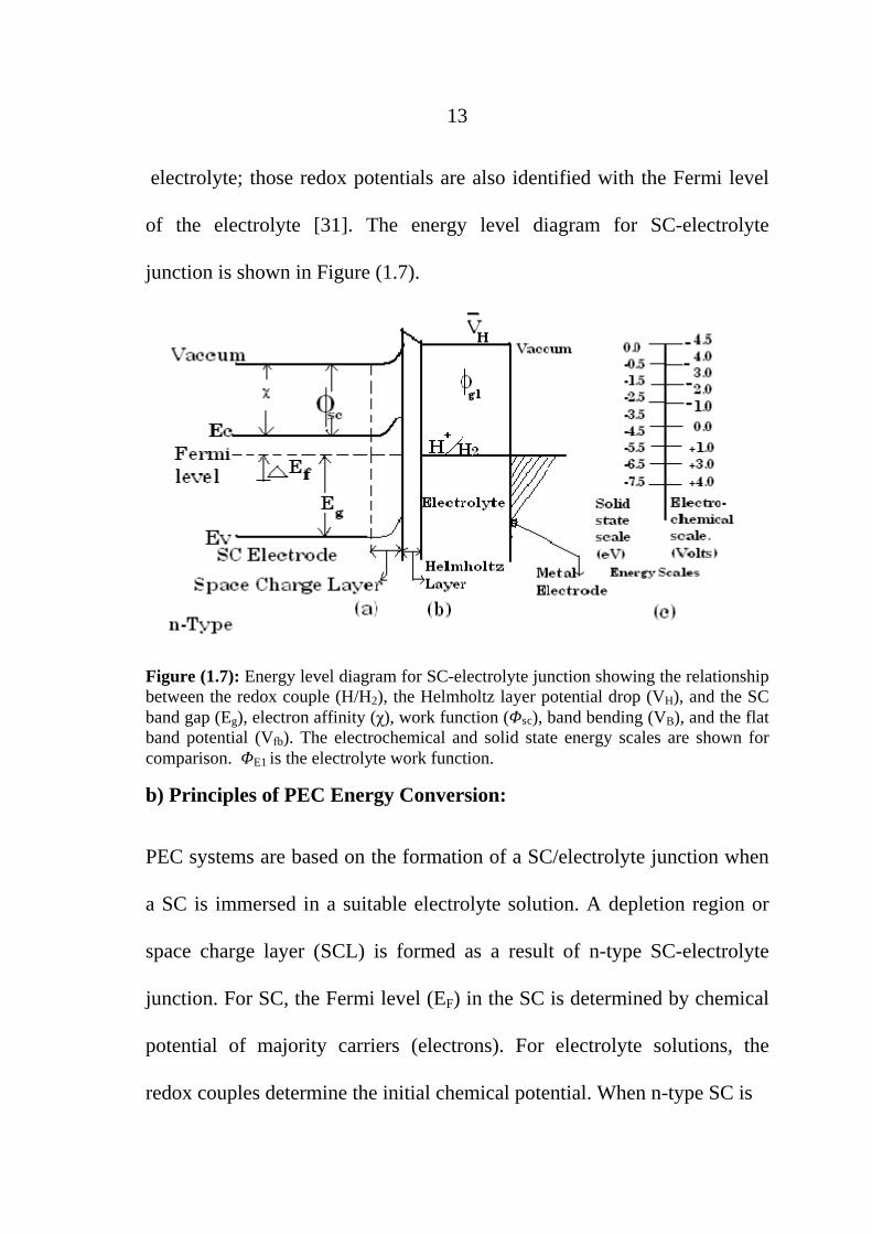
electrolyte; those redox potentials are also identified with the Fermi level
of the electrolyte [31]. The energy level diagram for SC-electrolyte
junction is shown in Figure (1.7).
Figure (1.7): Energy level diagram for SC-electrolyte junction showing the relationship between the redox couple (H/H2), the Helmholtz layer potential drop (VH), and the SC band gap (Eg), electron affinity ( ), work function ( sc), band bending (VB), and the flat band potential (Vfb). The electrochemical and solid state energy scales are shown for comparison. E1 is the electrolyte work function.
b) Principles of PEC Energy Conversion:
PEC systems are based on the formation of a SC/electrolyte junction when
a SC is immersed in a suitable electrolyte solution. A depletion region or
space charge layer (SCL) is formed as a result of n-type SC-electrolyte
junction. For SC, the Fermi level (EF) in the SC is determined by chemical
potential of majority carriers (electrons). For electrolyte solutions, the
redox couples determine the initial chemical potential. When n-type SC is

14
brought into contact with an electrolyte solution, the following energetics
will be exhibited. Before equilibrium the EF will remain above Eredox.
Electrons will therefore flow down to Eredox. As a result, EF will be lowered.
The electrons flow will continue until the equilibrium is established. At
equilibrium, EF and Eredox will match up. Consider an n-type SC and a
counter electrode in contact with the same electrolyte containing a redox
couple. The two electrodes are externally connected to each other with a
variable series load resistance R (0 < R< ); this type of PEC cell is called
regenerative cell, as shown in Figure (1.4-a ). At equilibrium the Fermi
level of the SC and the redox potential of the solution are adjusted in the
same level [32]. When the SC is illuminated the Fermi level of the SC will
Figure (1.8): Energy level diagram regenerative cell at:
equilibrium and (b) during illumination.

15
rise. The counter electrode Fermi level will also rise, depending on the
value of R. The rise of Fermi level depends on the rate of charge transfer at
the metal counter electrode. At R = 0 the electrodes are short
circuited
(sc) to each other, and they will have the same Fermi level. The excited
electrons will move through R to the counter electrode and reduce the ions
in the electrolyte as shown in Figure (1.4-b) [33].
1.11 Dark Current:
In the dark, at equilibrium, there exists a potential barrier between the
surface and the bulk of the electrode. The band bending in both valence and
conduction bands (VB) represents this potential. Occurrence of dark
current is due to electron transfer from the n-type SC conduction band to
the electrolyte across the interface. To achieve this, a negative potential
E) must be applied, to provide electrons with enough energy to
overcome this barrier, consequently no SCL will appear (flat band) [34].
Figure (1.9): Dark and photo currents observed in an n- SC/electrolyte PEC cell.

16
1.12 Photo Current:
When light absorption generates population of excited holes and electrons,
in n-type SC, the majority carrier concentration changes relatively little and
the minority carrier concentration is greatly enhanced. Hence photocurrents
are greatest when minority carriers dominate the electrode response. Photo
generated minority carriers (holes) migrate across the SC electrolyte
interface, with an oxidizing power to oxidize a red form of the redox
couple, and affect both photocurrent and photo potential:
h+ + red ox+ [35-36].
As an initial approximation photo effect switches on as the wave length of
the incident light ( ) decreases below the threshold wavelength ( g). With
shorter than g the electrode is relatively insensitive to light. A useful
relation between g and Eg [37] is : g =
Where g has units of nanometers, and Eg has units of (eV). The
dependence of photocurrent and photo potential on excitation wavelength
gives information about band gap energy and nature of optical transition
(direct or indirect). Recombination is another important phenomenon of
photo-effects in the PEC. Recombination can occur directly with the
electron descending from the conduction band to the hole edge at the

17
valance band edge, or indirectly via intermediate energy levels (bulk or
surface states) [38]. Recombination reduces the magnitude of photo effect,
and consequently lowers the power and the efficiency of PEC cell. When n-
type SC electrode is biased relatively positive of flat band VB the dark
currents are very low, due to blocking effect of the SCL. Upon the
irradiation of the SC through the electrolyte with light ( shorter than g ),
large anodic photocurrents appear. These photocurrents arise from the flux
of holes (minority carrier ) arriving at the surface . The generated electron
hole pairs in the SCL are separated by the electric field in the SCL.
Electron hole pairs, generated beyond the SCL, depends on the energy
distribution of the incident photons, the absorption coefficient of the SC,
the diffusion distance of the excited holes and electrons, and the
recombination rates [39]. As the applied potential approaches VB the space
charge layer thickness decreases. Recombination rates increase because the
holes and electrons are no longer being separated by the electric field. The
photocurrent drops sharply and merge with the dark current near VB. At
applied potential equals negative of VB, the electrode is no longer blocking
, and the dark current increases dramatically, with small anodic
photocurrent sometimes observed [40].

18
1.13 Perturbations of the Ideal Model of PEC Systems :
SC electrode behavior is not as ideal as discussed in the preceding section.
A number of phenomena occur that add a complication to the ideal model
i) Corrosion :
Rapid change in the surface composition results when the SC crystal
becomes in contact with the aqueous electrolytes. The photo- generated
holes and electrons are generally characterized by strong oxidation and
reduction potentials, respectively. Instead of being injected into the
electrolyte to drive redox reactions they cause SC surface corrosion [41].
Generally an oxide layer forms and causes SC surface decomposition. The
oxides include pH sensitivity of VB electrode surface. When current flows
across the solid liquid interface, the surface can undergo further
alteration. The most severe changes result when holes oxidizing
equivalents arrive at the surface. Thus n-type SC,s are particularly
susceptible to photo-corrosion. Both soluble and insoluble products may be
formed. The insoluble products build upon the surface, and may block
current flow [42].
19
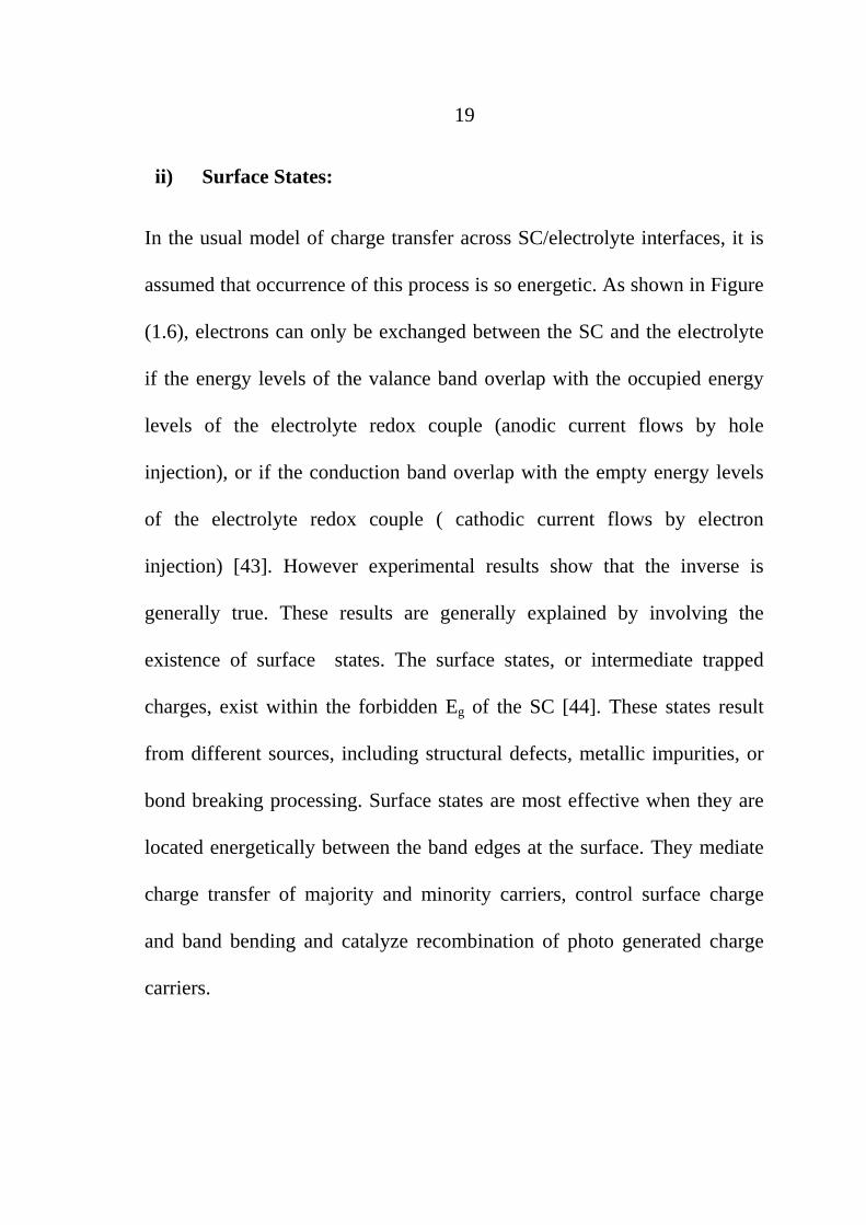
ii) Surface States:
In the usual model of charge transfer across SC/electrolyte interfaces, it is
assumed that occurrence of this process is so energetic. As shown in Figure
(1.6), electrons can only be exchanged between the SC and the electrolyte
if the energy levels of the valance band overlap with the occupied energy
levels of the electrolyte redox couple (anodic current flows by hole
injection), or if the conduction band overlap with the empty energy levels
of the electrolyte redox couple ( cathodic current flows by electron
injection) [43]. However experimental results show that the inverse is
generally true. These results are generally explained by involving the
existence of surface states. The surface states, or intermediate trapped
charges, exist within the forbidden Eg of the SC [44]. These states result
from different sources, including structural defects, metallic impurities, or
bond breaking processing. Surface states are most effective when they are
located energetically between the band edges at the surface. They mediate
charge transfer of majority and minority carriers, control surface charge
and band bending and catalyze recombination of photo generated charge
carriers.

20
Figure (1.10): Isoenergetic charge transfer of hole from n-type SC to
occupied state of electrolyte redox couple. Redox energy levels
have a distribution due to solvent-ion interactions.
The existence of surface states lowers the resulting photocurrent density.
Surface states may be classified as intrinsic or extrinsic [45]. Intrinsic states
arise from the abrupt termination of the crystal lattice at the electrode
surface. The dangling bonds in the crystal will dangle long in an
electrolyte. The new chemical entity formed by reaction with a solution
spieces may then behave as a surface state. Extrinsic states are created
when a new phase is formed at the interface, or when the electroactive
species (of the redox couple) adsorb to the electrode surface [46]. They are,
in principle, removable when the surface is renewed. Consider an n-type
SC in contact with an electrolyte containing an (ox) species, the standard
potential for the reduction of (ox) is more positive than VB Figure (1.7-a).

21
Surface states can provide an alternative path; the electrons tunnel through
the SCL to the surface states and then transfer to the (ox) spieces. The holes
in the valance band are captured by surface states in the band gap, which
then oxidize the red molecules, Figure (1.7-b).
The surface states overlap more effectively with the higher red energy
levels. The arrival of holes at the surface may create surface states [47].
Figure (1.11): Mediation of charge transfer by surface state at n-type SC.
a) Majority carrier injection through the barrier produced by band bending.
b) Photo-generated minority carrier injection via surface state.
iii) Doping Instability
If an electrode is biased in the depletion layer, very strong electric fields
are present in it. The field can act on charged donor and acceptor doping
species, causing them to migrate slowly in the crystal lattice. After

22
several hours or days of use, the doping density becomes inhomogeneous
near the electrode surface [48].
1.14 Types of Solar Cells:
a) Mono-Crystalline Electrodes:
They are the most developed and prevalent type in use today. These include
single crystal and polycrystalline silicon which is either grown or cast from
molten silicon and later sliced into desired cell size. These wafers are then
assembled onto a flat surface and covered with a protective tempered glass
surface. Single crystal silicon cells have the highest average efficiency
for converting solar energy into useful electricity. Polycrystalline silicon
cells, though a bit less efficient, are less expensive to manufacture [49].
b) Thin Films or Amorphous Electrodes:
They are inherently cheaper to produce than crystalline silicon but are not
efficient. They are produced by depositing a thin layer of photovoltaic
material onto a substrate like glass or metal. This material can be
encapsulated in building materials such as shingles to readily building-
integrated photovoltaic systems. Solar roofing materials allow PV to be
used in some circumstances where glass covered solar panels would not be
23
permitted or would be impractical. Solar shingles and roofing material tend
to be a bit more expensive than crystalline solar modules per quantity of
power produced [50].
1.15 Advantages and Disadvantages of PEC Cells:
There are several advantages of PEC cells for solar energy conversion over
PV devices:
(a) Energy can be stored in PEC devices in the form of conventional fuel.
(b) PEC cells do not contain solid-solid junctions and easy to fabricate.
(c) No problems occur in PEC cells due to thermal expansion as in PV
solid- solid junctions.
(d) No antireflection coatings are required in PEC cells [51].
The disadvantages of PEC cells are:
a) The absorption of light by the electrolyte solutions, b) Reflection
losses from the cell, and c) The unstability of the electrode. All these
lower the efficiencies in PEC cells [52].
1.16 Types of SC Materials for PEC Cells
The absorber material of SC in solar cell should be with acceptable price.
The following requirements should be fulfilled:

24
1) The band gap of the SC should be suitable for using maximum part
of solar spectrum.
) The efficiency of the cell should be high which depends upon
conductivity, diffusion length, band gap, surface state, etc.
The diffusion length is a measure of how far the doping density has
propagated in the substrate by diffusion in time t [53].
3) The electrode must be stable against corrosion when placed in redox
couple [54].
The most SC,s used in solar cells: are (Ge and Si), III-V compound (GaP,
InP, GaAs), II-compound (CdSe, CdS, CdTe), Transition metal di-
chalcogenides (MoSO2 and ZrS2), Oxide semiconductors (TiO2, WO3 and
ZnO), Zinc phosphides (Zn3P2), and Ternary compounds (CuInS2 and
CdIn2Se4) [55].

25
1.17 Earlier Studies on CdSe:
A number of techniques are employed in the formation of high quality thin
films such as, chemical vapor deposition, molecular beam epitaxial, pulsed
laser, evaporation and sputtering. Chemical bath deposition ( CBD) and
electro-deposition techniques are belonging to these alternative methods
that could also produce high quality films of chalcogenied materials. Effect
of many parameters on characteristics of CdSe thin films deposited by
CBD, were studied by G. Sarfa [56]. The variation of CdSe crystallite size
with annealing temperature is shown in Figure (1.8) [57].
Figure (1.12): Plot of CdSe crystallite size vs. annealing temperature
of CdSe thin films deposited by CBD technique [57].

26
The thickness evolution with time of the deposited layer is shown in Figure
(1.9). Annealing of thin films of CdSe has been studied by V. M. Garcia
[58]. Controlling the size of nanocrystals of CdSe was achieved by
changing the intensity of light illumination of growing film. The
nanocrystals radii were found between 1.9-10 nm.
Figure (1.13): Variation of CdSe film thickness with deposition time[59].
The effect of deposition parameters on the optical and electrical properties
of nanocrystalline CdSe was reported by Charita Mehta and coworkers
[60]. Analysis of optical absorption data to find the band gap has been
reported in the literature [61-64]. Other workers studied the improvement
of the prepared films by modification of the CBD preparation procedure.
The characteristics of the prepared films were investigated by measuring
their optical properties, structural morphology and chemical composition

27
[65]. The effect of parameters such as bath composition, deposition
temperature, pH of the solution, speed of the rotation and the specificity of
complexing agent on growth process was studied [66]. Scanning electron
microscopy (SEM) is a technique to study microstructure of thin film
Figure (1.10), (a) and (b) shows the SEM micrographs of as-deposited and
annealed at 673 K of CdSe thin films.
Figure (1.14): SEM of CdSe thin films (a) as-deposited and
(b) annealed at 673 K [67].
From SEM studies, it is observed that the as deposited CdSe films are
nanocrystalline, homogeneous without cracks or holes and well covered to
the glass substrate.

28
Despite that, to our knowledge there are many important studies that have
not been conducted on CdSe thin films. Examples of such studies are:
1) Deposition of CdSe thin films onto FTO glass by CBD.
2) The PEC study of CdSe films on FTO, prepared by CBD.
3) Effect of cooling rate on CBD made CdSe films, on FTO, on its
characteristics.
4) Surface modification of CdSe film electrodes, prepared by CBD
onto FTO.
1.18: Major Theme of This Study:
The major themes of this study are:
1) Preparing CdSe thin films deposited onto FTO glass by CBD.
2) Trying to use CdSe films deposited onto FTO/glass substrates as
electrodes in light to-electricity conversions under PEC
conductions.
3) Trying to enhance CdSe thin film electrode efficiency and stability
by controlling cooling rate of pre-annealed samples.

29
4) Coating the CdSe thin film electrodes with electroactive
metalloporphyrine complex embedded in polysiloxane polymer matrices
and investigate the effect on their PEC characteristics.
5) In parallel to PEC characteristics, effect of treatment on other
properties such as absorption spectra and photoluminescence emission
spectra will also investigated.

30
Chapter Two
Experimental Work
2.1 Materials
2.1.1 Chemicals and Solvents
Starting materials, such as Se, S, K3Fe(CN)6, K4Fe(CN)6, LiClO4, KOH,
CdCl2.2H2O, Na2SO3, Na2S, were purchased from Aldrich, HCl was
purchased from Frutarom, and methanol from Riedel-DeHa n.
2.1.2. Preparation and Characterization of MnP:
The tetra(-4-pyridy1)porphyrinatomanganese(III)sulfate (MnP) complex,
Figure (2.1), was prepared from H2TPyP (81.7 mg, 0.132 mmol) was
vigorously refluxed with excess manganese (II) sulfate (1.53g, 0.91 mmol)
in N, N-dimethylformamide, DMF, (60 ml) for 10h. The solution was
concentrated by evaporating DMF under reduced pressure. Air was passed
through the reaction mixture to oxidize Mn2+ to Mn3+. The reaction mixture
was then ion-chromatographed over activated neutral alumina using DMF
as eluant. Eluate fractions with the characteristic absorption bands at 462,
569 and 620 nm, [68], were stored in the dark [69].

31
Figure (2.1): MnP polymer [70]
The mixture contained complexes of both the MnII and the MnIII , as
depicted from the electronic absorption spectra in the visible region,
Figures (2.2-2.5).
Figure (2.2): The electronic absorption spectra in
UV/ visible region for MnP solution in methanol [71].
Figure (2.3): The electronic absorption spectra in the UV/visible
region for MnP embedded into a polysiloxane polymer solid matrix [72].

32
Figure (2.4): The electronic absorption spectra in the UV/visible Region for MnP embedded into a polysiloxane polymer solid matrix
after annealing at 150
for 30 min. under N2 atmosphere [ 73].
Figure (2.5): The electronic absorption spectra in the UV/visible region for solid polysiloxane membrane [74].
2.1.3 Etching Process
The prepared electrodes of CdSe to be etched were treated by dilute HCl
(10 ) solution. The electrode was immersed in the dilute solution of HCl
for about 5 seconds and then rinsed with distilled water and methanol then
dried with nitrogen. The above procedure was for obtaining a shiny film
surface.

33
2.1.4 Preparation of CdSe Thin Films
Chemical bath deposition technique was adopted for the preparation of the
cadmium selenide thin films. The deposition of thin films was on glass
plates covered by Fluorine-doped Tin Oxide (FTO) thin film. The
experimental arrangement is shown in Figure (2.6). It consists of a
chemical bath of Na2SO3 and Se [75]. Ordinarily, selenium is not soluble in
water. In order to create selenium ions in the form of sodium selenosulphite
(Na2SeSO3), selenium powder was mixed with sodium sulphite solution
and heated to 900C for about 9 to15 hours. The resulting Na2SeSO3
becomes the source of Se-2, while the source of Cd+2 is the cadmium
chloride (CdCl2.2H2O). Ammonia was used as a comlexing agent. To
prepare 300 ml of Na2SeSO3 solution, 60 gm of Na2SO3was added to 300
ml of distilled water, then 6 gm of Se powder was added to the solution.
After stirring for 15 hours at 900C, fresh Na2SeSO3 solution is filtered. In
another beaker, 30 gm of CdCl2.2H2O was added to 300 ml of distilled
water, then 25
NH3 solution was added to the solution with constant
stirring until milky turbid Cd(OH)2. Further addition of excess ammonia
dissolved turbidity and made solution clear. To this mixture, 300ml of
freshly prepared Na2SeSO3 was added slowly with constant stirring [76].
34
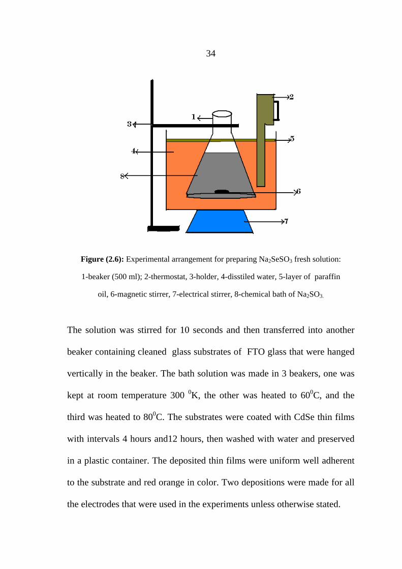
Figure (2.6): Experimental arrangement for preparing Na2SeSO3 fresh solution:
1-beaker (500 ml); 2-thermostat, 3-holder, 4-disstiled water, 5-layer of paraffin
oil, 6-magnetic stirrer, 7-electrical stirrer, 8-chemical bath of Na2SO3.
The solution was stirred for 10 seconds and then transferred into another
beaker containing cleaned glass substrates of FTO glass that were hanged
vertically in the beaker. The bath solution was made in 3 beakers, one was
kept at room temperature 300 0K, the other was heated to 600C, and the
third was heated to 800C. The substrates were coated with CdSe thin films
with intervals 4 hours and12 hours, then washed with water and preserved
in a plastic container. The deposited thin films were uniform well adherent
to the substrate and red orange in color. Two depositions were made for all
the electrodes that were used in the experiments unless otherwise stated.

35
2.1.5 Annealing Process
Annealing was conducted using a thermo stated horizontal tube furnace.
The prepared CdSe film substrates were inserted in the middle of a long
Pyrex cylinder. The heat was raised to the desired temperature (100,150,
200, 250, 300, 350) 0C, under air pressure. The sample was kept at that
temperature for 20 min before being allowed to cool. The annealing system
was shown in Figure (2.7).
Figure (2.7): The annealing system
2.1.6 Cooling Process
a) Quenching (Fast Cooling)
The furnace was switched off. The heated system (Pyrex cylinder and film
substrate) was taken from the furnace left to cool under air from the desired
temperature to room temperature within about 3 minutes.
36
b) Slow Cooling Process:
After 20 min of heating at desired annealing temperature, the oven
temperature was lowered by 50 0C. After the reading temperature reached
the setting temperature, the oven temperature was lowered by 500C, again.
This procedure was repeated until room temperature was reached, through
step wise process, with 500C lowering in each step. Rate of cooling was
100 0C per hour on the average.
2.2 Equipment
2.2.1 Measuring Devices
The measurements of current voltage data were performed using a
computer controlled Princeton Applied Research (PAR) Model 263A
potentiostat. Light intensity was measured with Lutron LX 102 light
meter. The light meter, which measures the luminance in lux units, was
calibrated against a Kipp and Zonen CM11 pyranometer. UV absorption
spectra were measured on a Shimadzu UV-1601 spectrophotometer. PL
emission spectra were measured on a Perkin Elmer LS50B Luminescence
spectrometer Figure (2.8). PL spectra of films of CdSe on FTO glass where
directly measured using excitation wavelength 250 nm.

37
Figure (2.8): Schematic diagram showing measurements of the PL emission spectra
using Perkin Elmer, luminescence spectrometer LS50B.
2.2.2 PEC Cell
The prepared CdSe film electrode was incorporated as a working electrode
into a three electrode one-compartment photoelectrochemical cell, with a
platinum counter electrode and reference saturated calomel electrode, SCE,
Figure (2.9). Two types of electrolyte solutions were used in this work.
The first was: 0.1M of LiClO4, 0.05 M of K3Fe(CN)6 and 0.05 M of
K4Fe(CN)6. The second was: 0.1 M of (Na2S, S, KOH), all in distilled
water. In each case high purity nitrogen (99.999%) was bubbled through
the solution for at least 5 minutes before each experiment, and was kept to
bubble over the solution during the experiment to minimize contamination
with air.

38
Figure (2.9): Three electrode photoelectrochemical cell (PEC).
2.2.3 Light Source
For illumination 50 watt Xenon lamp was used, with a housing and a
concentrating lens. This lamp has an intense converge of wide spectral
range between (450-800) nm with a high stability. The lamp was placed at
a certain distance from the working electrode. The illumination power on
the electrode was about 0.0212 W. cm-2.
2.3 PEC Measurements
2.3.1 Current Density Potential Plots
Current density (J-V) plots were measured using the PEC cell shown in
Figure (2.8), at room temperature. Nitrogen atmosphere was kept above the

39
solution. The photocurrent measurements were done using a 50 watt
Xenon lamp; but the dark current ones were done under complete dark
using thick blanket cover. The measurements of current voltage data were
performed using a computer controlled Princeton Applied Research (PAR)
Model 263A Potentiostat/Galvanostat. The measured current (I) was
converted into current density (J), by dividing the current I by the area of
the illuminated electrode.
2.3.2 Stability Testing
Using the same PEC, short circuit current density (Isc) values were
measured over a range of time periods. Short circuit current density(Jsc)
were calculated by dividing values of Isc by electrode area (cm2). The
light was maintained during the measurements on the electrode, with
steady illumination (0.0212)W.cm-2, and under 0.00 V bias, at room
temperature. Effect of electrode annealing and cooling rate were studied.
2.4 UV/Visible Absorption Spectra Measurements
UV absorption spectra were measured for substrates annealed at different
temperatures. Some of the electrodes were quenched, others were slowly
cooled, and one was not annealed. A Shimadzu UV-1601
spectrophotometer was used for absorbance measurements. Gas

40
Chromatography/Mass Spectrometry analysis was conducted on a
Shimadzu GCMS-QP 5000.
2.5 Photoluminescence (PL) Emission Spectra
Photoluminescence emission spectra were measured for different
substrates:
a) For substrates annealed at different temperatures (100, 200, 350) 0C,
slowly cooled and one not annealed, all prepared at room temperature.
b) For substrates annealed at (100, 200, 350)0C, quenched and one not
annealed, all prepared at room temperature.
All the measurements were made with excitation 250nm. A cut off filter
(shorter than 500 nm removed) was used between the sample and the
detector.
2.6 Coating The Electrodes With a Polymer
In order to enhance CdSe film contact with FTO, the glass/FTO electrodes
were gently polished with fine glass paper. This was to allow better contact
between CdSe films with FTO.
Covering the electrodes with a polymer was conducted as follows: A
dilute solution, of commercial RTV made polysiloxane paste in acetic acid,
was prepared by dissolving 0.01 mg of the paste in 20.0 ml of

41
dichloromethane. Similarly, an MnP solution was prepared by dissolving
(0.01 mg, 1.38 × 10 5 mol) in 1.0 ml methanol. The MnP/polysiloxane
stock solution was prepared by adding the MnP solution to the polysiloxane
solution in a 1:4 (V/V) ratio, respectively. Then 0.1 ml of the
MnP/polysiloxane stock solution, containing 4.0 × 10 5 g polysiloxane and
2.0 × 10 4 g MnP, were coated onto the preached CdSe polished surface.
The substrate was immersed in the solution for 4 seconds. The organic
solvent mixture, dichloromethane/methanol, was then allowed to evaporate
off, leaving a transparent thin layer of MnP/polymer matrix on the surface
of electrode. With thicker films than 4 m, the polymer matrix worked as
insulator and allowed no current to be measured. All SC electrodes were
coated using thickness about 4 m. In control experiments, CdSe surfaces
were modified with a thin polysiloxane film and MnP. The modified
electrode was further annealed, after fabrication, at 1000C for 30 min under
nitrogen. The system was then left to cool at room temperature under N2
[77].

42
Methyltriacetoxysilane
Tetra-4 pyridylporphyrinatomanganese(III) complex.
Figure (2.10): Compounds of the polymer used for coating the CdSe thin films.
2.7 Measuring the Thickness of CdSe Layer
The thickness of the layer was measured by two ways:
1) By optical microscopic measurement which gave approximately less
than 20 m thickness.
2) By a micrometer which was ( 10 m).

43
Chapter Three
Results
General Remarks
Chemical bath deposition technique was used in this work to prepare thin
films of CdSe onto glass substrates. The prepared films were treated by
annealing at different temperatures, (100,150, 200, 250, 300, 350) 0C under
air. Two different methods were used to cool the annealed films to room
( 25 0C) temperature; quenching or slow cooling. Effects of annealing and
cooling rate on UV/Visible absorption spectra of the prepared thin films
were measured. Treated and untreated films were studied as electrodes in
PEC system. The main objective was to see optimal conditions that yield
highest electrode efficiency and stability under irradiation. Two redox
couple systems were tested in the PEC measurements. In order to enhance
efficiency and stability of the CdSe electrodes, they were coated with
MnP/polysiloxane polymer matrices. The treated wafers were then used as
PEC electrodes for light to-electricity conversion. The treatment affected
dark J V plots, photo J V plots, SC efficiency and stability.
3.1 Enhancement Studies of Uncoated CdSe Film Electrodes
As reported by [78], thick matrices of MnP/polysiloxane more than 4 m
showed bad J-V plots for current readings. Therefore, thin matrices, about
4 m thick were made to lower the resistance. Figures (3.17-30) show that

44
annealing and then coating the surface of CdSe by MnP/polysiloxane
matrix enhanced the J-V plots for both dark current and photo current.
These two processes also enhanced the stability and efficiency of CdSe thin
wafers.
3.1.1 UV/Visible Absorption Spectra:
Figure (3.1) shows the UV/Visible spectra for the untreated CdSe film.
Figure (3.2) shows absorption spectra measured for pre-annealed CdSe thin
films at 1000C, quenched and slowly cooled samples. The Figures indicate
that pre-annealing CdSe films gives better absorption spectra with well
defined sharp absorption bands. This indicates that pre-annealing, at 100oC,
enhances physical properties of CdSe mictocrystals, despite cooling rate.
The slope at right side in Figure (3.1) is not good.
Figure (3.1): UV/Visible absorption spectra, for nonannealed CdSe thin film.
45
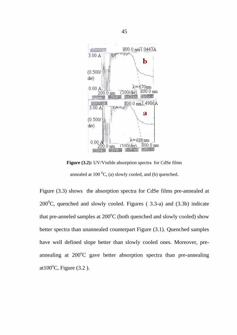
Figure (3.2): UV/Visible absorption spectra for CdSe films
annealed at 100 0C, (a) slowly cooled, and (b) quenched.
Figure (3.3) shows the absorption spectra for CdSe films pre-annealed at
2000C, quenched and slowly cooled. Figures ( 3.3-a) and (3.3b) indicate
that pre-anneled samples at 200oC (both quenched and slowly cooled) show
better spectra than unannealed counterpart Figure (3.1). Quenched samples
have well defined slope better than slowly cooled ones. Moreover, pre-
annealing at 200oC gave better absorption spectra than pre-annealing
at100oC, Figure (3.2 ).

46
Figure (3.3): UV Absorption Spectra, CdSe annealed at 200 0C,
(a) slowly cooled, and (b) quenched.
Figure (3.4 ) indicates that UV-absorption spectra for CdSe electrodes, pre-
annealed at 3500C did not show singificant enhancement compared to un-
annealed counterpart. The Figures show that annealing at 200oC gives
samples with best absorption spectra.

47
Figure (3.4): UV-Absorption Spectra for CdSe electrode, annealed
at 350 0C, (a) slowly cooled, and (b) quenched.
The band gaps for CdSe films were calculated from UV-spectra as shown
in Table (3.1). A line which is extrapolated to the slope at right side of each
spectrum, has an intersection with the x-axis. This intersection gives .
Then: Eg = 1240/ This is done for each value of Eg. Annealing showed
lowering in band gap value, from 2.0 to 1.7 eV measured for CdSe films
deposited onto FTO glass surfaces here. Literature showed lowering from
2.3 to 1.8 eV by annealing CdSe deposited onto glass substrates [79].

48
Table (3.1): Band gap values, for CdSe thin films, measured from UV/Visible spectra.
Band gap Eg
(eV) deposited
onto glass [70].
Band gap Eg (eV). Prepared CdSe thin
film.
2.3 2.0 Non-annealed
2.0 1.85 100 C (quenched)
- 1.83 100 C (slowly cooled)
1.8 1.91 200 C (quenched)
- 1.88 200 C (slowly cooled)
1.7 1.80 350 C (quenched)
350
(slowly cooled)
1.94 -
Figures (3.2 )
(3.4 ) show that cooling rate affects UV/Visible absorption
spectra for CdSe films. In each annealing temperature, the quenched
samples showed better spectra with more defined absorption.
3.1.2 Photoluminescence Emission Spectra:
Figure (3.5) shows the PL emission spectra for untreated CdSe film as in
Figure (3.5-d) spectrum. PL spectra for annealed (quenched) CdSe films at

49
temperatures 100 , 200
and 350 , are shown in curves (c, a and b) in
Figure (3.5) respectively. The spectra in Figure (3.5) indicate that pre-
annealing CdSe films gives higher emission intensity than the non annealed
films. The sample annealed at 200 has the best spectrum with highest
emission intensity. This indicates that pre-annealing enhances physical
properties of CdSe mictocrystals, despite cooling rate. Figures (3.5 ) and
(3.6 ) show that cooling rate affects PL emission spectra for CdSe films.
For the sample annealed at 200 , the slow cooling is better than the
quenched one. For other annealing temperatures, the quenched samples
showed better spectra with higher defined emission intensity.
Figure (3.5): quenched thin films, prepared at room temperature.
50
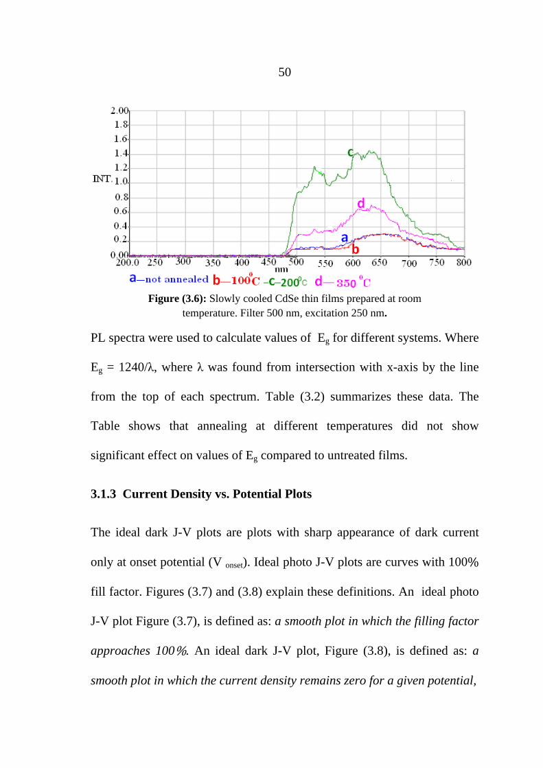
Figure (3.6): Slowly cooled CdSe thin films prepared at room temperature. Filter 500 nm, excitation 250 nm.
PL spectra were used to calculate values of Eg for different systems. Where
Eg = 1240/ , where was found from intersection with x-axis by the line
from the top of each spectrum. Table (3.2) summarizes these data. The
Table shows that annealing at different temperatures did not show
significant effect on values of Eg compared to untreated films.
3.1.3 Current Density vs. Potential Plots
The ideal dark J-V plots are plots with sharp appearance of dark current
only at onset potential (V onset). Ideal photo J-V plots are curves with 100
fill factor. Figures (3.7) and (3.8) explain these definitions. An ideal photo
J-V plot Figure (3.7), is defined as: a smooth plot in which the filling factor
approaches 100 . An ideal dark J-V plot, Figure (3.8), is defined as: a
smooth plot in which the current density remains zero for a given potential,

51
and suddenly it drops negative at the onset potential (V onset).
Table (3.2): Band gap values, for CdSe thin films, calculated from PL emission spectra.
Prepared CdSe thin film Band gap Eg (eV)
Non-annealed 1.90
100
(quenched) 1.89
100
(slowly cooled) 1.88
200
(quenched) 1.94
200
(slowly cooled) 1.97
350
(quenched) 1.88
350
(slowly cooled) 1.97
Figure (3.7): Ideal photo J-V plot for SC. Figure (3.8): Ideal dark J-V plot for SC.

52
3.1.4 The Effect of Redox Couple
a) Dark J-V Plots for CdSe Electrode
The dark J-V plots for CdSe electrodes were obtained in a redox couple
which consists of [LiClO4, K3Fe(CN)6, K4Fe(CN)6]. Measurements were
performed using unheated electrodes, annealed electrodes at different
temperatures, quenched electrodes and slowly cooled ones. Film deposition
was conducted at room temperature. The CdSe films were broken down in
the solution of the redox couple. All electrodes showed poor dark J-V plots.
Figures (3.9)-(3.10) are presented only as examples to show such poor
plots.
Figure (3.9): Dark J-V plot for CdSe electrode, annealed at 100
and quenched, in redox solution of 0.1M LiClO4, 0.05M of K3Fe(CN)6, K4Fe(CN)6.

53
Figure (3.10): Dark current J-V plot for not-annealed
CdSe electrode in redox solution of
0.1 M LiClO4, 0.05 M of K3Fe(CN)6, K4Fe(CN)6.
b) Photo J-V Plots for CdSe Electrode
Many measurements were performed for nonannealed and annealed CdSe
thin films at different temperatures and cooled either by quenching or
slow cooling. All measurements for photo J-V plots of CdSe thin films
gave so poor results and resembled conductor behavior. No
semiconductor behavior was observed. Experiment were conducted in the
redox couple system described earlier. Wafers were spoiled, and pieces of
them peeled off in the redox couple solution. Figures (3.11)-(3. 12) show
examples of some of poor J-V plots.

54
Figure ( 3.11 ): Photo J-V plot for not annealed CdSe electrode in redox couple
solution 0.1 M LiClO4, 0.05 M K3Fe(CN)6 and K4Fe(CN)6.
Figure (3.12 ): Photo J-V plot for CdSe electrode, annealed at 4000 C,
in redox couple solution 0.1 M LiClO4, 0.05 M of K3Fe(CN)6 and K4Fe(CN)6.
When another redox couple was used, the results for nonannealed,
annealed, (quenched or slowly cooled) CdSe thin films were all poor. The
redox couple used was 0.1M of each: S, Na2S, KOH. Examples of poor

55
results obtained are shown in Figures (3.13) and (3.14).
Figure (3.13): Dark J-V plot for CdSe electrode annealed at 3500C, quenched in 0.1 M (S, Na2S, KOH).
Figure (3.14): Photo J-V plot: not annealed, two depositions,
in redox couple 0.1 M of ( KOH, S, Na2S ).

56
Figure (3.15) shows pictures of a number of CdSe /FTO/glass electrodes
taken after use in PEC experiments. CdSe peeling off is obvious as
complete removal of CdSe films was observed.
(a) (b) (c) (d)
.Figure (3.15): Spoiled electrodes due to the broken down of the CdSe wafer in both
redox couples used. a) Not annealed. b) Quenched from 1500C
c) Slowly cooled from 2000C d) Quenched from 4000C.
In order to improve contact between CdSe films and FTO, the FTO surface
was roughed by fine sand paper, prior to CdSe film deposition. The
resulting CdSe/FTO/glass electrode showed some enhancement, and
semiconductor behavior was observed, Figure (3.16). However, no
significant enhancement was observed, and further modification is needed
to be made.

57
Figure ( 3.16): Photo J-V plots for CdSe film electrode, annealed to 3500C,
quenched in redox couple 0.1 M (KOH, S, Na2S). The FTO/glass
was treated with sand paper prior to CdSe deposition.
3. 2 Effect of Coating CdSe Thin Films with Mn/Polysiloxane:
Both electrode efficiency and stability of n-GeAs were significantly
enhanced by coating the electrodes with porphyrinatomanganese (III and
II) couple, MnP, embedded inside polysiloxane matrices [80-82]. To
improve adherence of CdSe film, FTO was roughed by fine paper before
CdSe deposition, and small enhancement in J-V plots were obtained.
To obtain more enhancement, the electrodes were coated with
porphyrinatomanganese (III and II) couple, MnP, embedded inside
polysiloxane polymer matrices. The treatment affected dark J V plots,
photo J V plots, SC efficiency and stability, under PEC conditions.

58
a) Dark J-V Plots with Polymer
Coating with porphyrinatomanganese, MnP, embedded inside polysiloxane
matrices enhances dark current J-V plots for nonannealed electrodes.
MnP/polysiloxane-modified electrodes showed better dark J V plots than
uncoated electrodes. The modified electrodes did not peel out in the
solution of the redox couple. Figure (3.17) shows that the dark current J-V
plots for MnP/polysiloxane modified electrodes show typical diode
behaviors in the dark. Pre-annealing of the MnP/polysiloxane modified
electrodes at 100 , 200 , 250 , 300 , 350
enhance J-V plots in the
dark. These are shown in Figures (3.18-23). Note that CdSe film pre-
annealing was conducted before coating with MnP/polysiloxane matrix.
After coating with MnP/polysiloxane matrix, each electrode was annealed
for 30 minutes, then dried under N2 atmosphere.

59
Figure ( 3.17 ): Dark J-V plots for MnP/polysiloxane coated CdSe electrodes, (a)
unannealed, the others are annealed at 1000C,
b) slow cooling, c) quenched.
Figure (3.18): Dark J-V plots for MnP/polysiloxane coated CdSe
electrodes, (a) unannealed, the others are annealed at 150 ,
(b) slowly cooled, (c) quenched.

60
Figure ( 3.19): Dark current J-V plots for MnP/polysiloxane
coated CdSe electrodes (a) unannealed, the others are annealed at 2000 C,
(b) slowly cooled, (c) quenched.
Figure ( 3.20): Dark J-V plots for MnP/polysiloxane
coated CdSe electrodes (a) unannealed, the others are annealed at 2500C,
(b) slowly cooled, (c) quenched.

61
Figure ( 3.21): Dark J-V plots for MnP/polysiloxane coated CdSe electrodes, (a) unannealed, the others are annealed at 3000C,
(b) slowly cooled, (c) quenched.
Figure (3.22): Dark J-V plots for MnP/polysiloxane coated CdSe electrodes (a) unannealed, the others are annealed at 3500C, b) slow
cooling, (c) quenched.

62
Figure (3.23): Dark J-V plots for MnP/polysiloxane
coated CdSe electrodes: (a) un annealed, others are
quenched from: b) 1000C,
c) 1500C, d) 2000C, e) 2500C,f) 3000C, g) 350 0C.
Figures (3.17) through (3.23) summarize results of dark J-V plots
MnP/polysiloxane coated CdSe electrodes.Figures (3.17)- (3.23) indicate
that quenched CdSe electrodes, from different temperatures showed better
or similar dark-current J-V plots than slowly cooled electrodes. Figure
(3.17) shows that slowly cooled and unannealed electrode has aproxematly
the same dark J-V plot. Quenched electrpde from 100
is better than the
slowly cooled and unannealed ones. Figure (3.18) shows that quenched
electrode from 150
is better than slowly cooled, which in turn is better
than unannealed one. At temperatures 200 , 250
and 350 , dark J-V
plots for quenched electrodes are better or similar to slowly cooled
63
electrodes. Figure (3.23) shows that the dark J-V plot quality was in the
order: 200
250
300
350
150
100 .
b) Photo J-V Plots for MnP/polysolixane Coated CdSe Electrodes:
Figures (3. 24-3.28) show that photo J V plots measured for
MnP/polysiloxane-coated SC electrodes were improved by preannealing
compared to untreated electrodes. Significant J-V plot enhancement was
observed by annealing. Treated electrodes are better than the untreated
ones as observed from J-V plot shape, fill factor and value of short circuit
current. In addition to photocurrent J-V enhancement by coating with
MnP/polysiloxane, further enhancement can be achieved by preannealing
the CdSe thin films. Figures (3.24) through (3.28) indicate that
preannealing of CdSe film electrodes followed by MnP/polysiloxane
polymer coating, significantly enhances photo J-V plots. Moreover, cooling
rate of preannealed CdSe, affects photo J-V plots for MnP/polysiloxane
coated electrodes. Figures (3.24) through (3.28) summarize these findings.

64
Figure (3.24 ): Photo J-V plots for MnP/polysiloxe coated CdSe electrodes, (a) unannealed,the others are annealed at 1500 C
, (b) slowly cooled and (c) quenched .
Figure ( 3.25): Photo J-V plots for MnP/polysiloxane
coated CdSe electrodes (a) unannealed, the others are annealed at 2000 C,
(b) slowly cooled (c) quenched.

65
Figure (3.26): Photo J-V plots for MnP/polysiloxane coated CdSe electrodes, (a) unannealed, the others are annealed at 2500C.
(b) slowly cooled, (c) Quenched.
Figure (3.27): Photo J-V plots for MnP/polysiloxane coated CdSe electrodes (a) unannealed, the others are annealed to 300 0C,
, (b) slowly cooled, (c) quenched.

66
Figure (3.28): Photo JV plots for MnP/polysiloxane coated CdSe electrodes (a) unannealed, the others are annealed at 3500C
b) slowly cooled, (c) quenched.
In Figure (3.25), the electrode quenched from 2000C gives the best
efficiency in comparison with other electrodes. Figure (3.25) shows that the
electrode quenched from 2000C is better than the slowly cooled electrode.
Figures (3.24-28) also show that quenched electrodes have better or similar
photo J-V plots than slowly cooled counter parts. Among the CdSe
electrodes, coated with MnP/polysiloxane, prequenched from different
temperatures, the photo J-V plot quality was in the order: 2000C 2500C
3000C 3500C 1500C unannealed.

67
Figure (3.29): Photo J-V plots for MnP/polysiloxane coated
CdSe electrodes quenched from (a) unannealed, (b) 1500C,
(c) 2000C (d) 2500C, (e) 3000C (f) 3500C.
Figure (3.30): Photo J-V plots for MnP/polysiloxane coated CdSe
electrodes slowly cooled from: (a) unannealed, (b) 1500C, (c) 2000C,
(d) 2500C, (e) 3000C, ( f) 350 .

68
Coating with MnP/polysiloxane, protected the CdSe film from peeling out.
Figure ( 3.31) shows pictures of different films after exposure to PEC
conditions.
Figure (3.31): Some electrodes after coating MnP/polysiloxane, and after using in PEC. a) Pre-Annealed at 150 , b) Annealed at 200 ,
c) Annealed at 250 , d) Annealed at 300 .
Comparing coated electrodes in Figure (3.31) with that in Figure (3.15), we
see that the coated ones are not broken down in the redox couple.
c) Electrode Stability
The stability of the MnP/polysiloxane coated CdSe electrode, under PEC
conditions, was studied. Values of short circuit current density (Jsc) were
measured over a range of periods of time, while keeping the electrode
under steady illumination (0.0212Wcm 2) and under a 0.00 V bias vs. SCE.
Plots of values of Jsc vs. time were constructed as shown in Figures
(3.32-34).
69
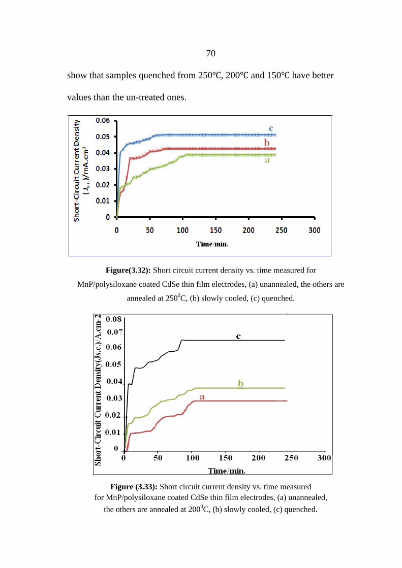
d) Effect of Annealing on Electrode Stability:
Effect of preannealing on MnP/polysiloxane covered CdSe film stability
has been studied using redox couple which is 0.1 M of (S, Na2S, KOH)
under illumination. Plots of I s.c .vs. time have been constructed for
untreated electrodes and pre-heated/pre-cooled ones from 2500C using slow
and rapid cooling. Figures (3.32-34) show these results. In each plot, the Js.c
. starts with very small values, and increases with time until a steady value
was reached. This demonstrate the stability of CdSe thin films under PEC
conditions for as long as 250 min. It is clear that the pre-heated electrodes
gave higher Js.c .values than untreated ones. Figure (3.32) shows that the
electrode pre-annealed at 250 has better Js.c .value than unheated one.
Figure (3.33) shows that electrodes annealed at 200
have better Js.c.values
that the un annealed one. Figure (3.34) shows that quenched electrode from
150
has better values than the slowly cooled one. Among different
temperatures used, the 200
was the optimal annealing temperature. For
quenched samples, values of Js.c .varied in the order: 200
250
150
un annealed.
e) Effect of Rate of Cooling on Electrode Stability:
Effect of cooling rate on stability of MnP/polysiloxane coated CdSe
electrodes under PEC conditions was studied. Figures (3.32-34)
70
show that samples quenched from 250 , 200
and 150
have better
values than the un-treated ones.
Figure(3.32): Short circuit current density vs. time measured for
MnP/polysiloxane coated CdSe thin film electrodes, (a) unannealed, the others are
annealed at 2500C, (b) slowly cooled, (c) quenched.
Figure (3.33): Short circuit current density vs. time measured for MnP/polysiloxane coated CdSe thin film electrodes, (a) unannealed,
the others are annealed at 2000C, (b) slowly cooled, (c) quenched.

71
Figure (3.34): Short circuit current density vs. time measured
for MnP/polysiloxane coated CdSe thin film electrodes, (a) unannealed,
annealed at 1500C, (b) slowly cooled, (c) quenched.
Figure (3.33 a and b) shows that the electrode quenched from 2000C (3.33-
a) has higher Js.c. values than slowly cooled electrode. This result is
consistent with previous results. Figure (3.34 a and b) shows similar result
for 150 . The CdSe thin film quenched from 200
gives the best value,
followed by the one quenched from 250
, and the one quenched from
150 ,the slow cooled sample from 250
respectively.
f) Cell Efficiency Studies:
MnP/polysiloxane modification of CdSe thin films enhances the light-to-
electricity conversion efficiency. Table (3.3) shows the data of
Efficiency ( ), open circuit potential (Vo.c.), short circuit current density

72
(Js.c. ) and fill factor (FF ) for different electrodes. The Table shows the
different PEC characteristics for pre-heated electrodes are higher than for
non-heated ones. The Table also shows that the Js.c. and efficiency values
for quenched electrodes are higher than those for slowly cooled ones,
except for electrode heated at 250
which has the same values for
quenched and slowly cooled ones. The best value of efficiency is that for
electrode quenched from 200 . For slowly cooled ones the best efficiency
is for 250 200 is still higher
Open circuit potential and fill factor for slowly cooled electrodes are higher
than or equal for quenched electrodes, as shown in Table (3.3).
Among different electrodes, the slowly cooled electrode from 200
showed highest FF value.

73
Table (3.3): Values of efficiency ( ), open circuit voltage (Vo.c.), current density( Js.c.)
and for fill factor (FF) for MnP/polysiloxane coated CdSe film.
*All measurements were conducted in aqueous (KOH, S, H2S) at 25 C.
** ( ] 100 .
***FF=[(maximum observed power)/Is.c. Vo.c.] 100 .
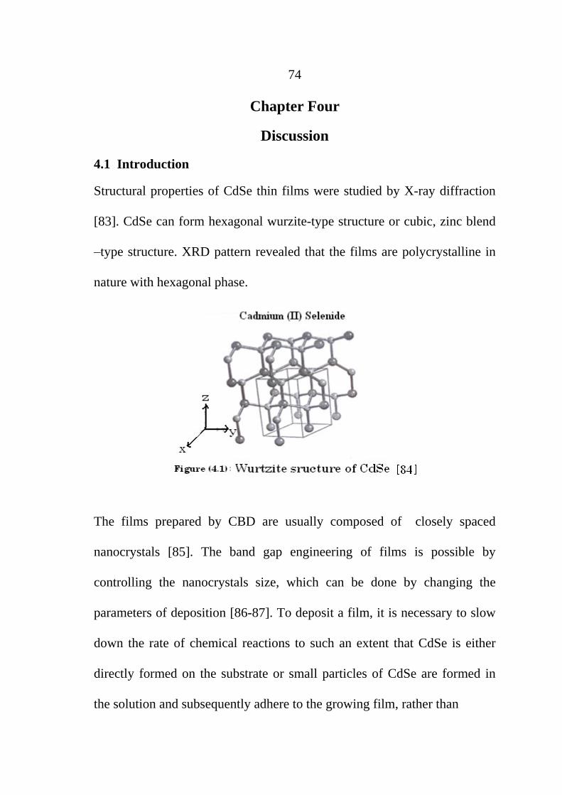
74
Chapter Four
Discussion
4.1 Introduction
Structural properties of CdSe thin films were studied by X-ray diffraction
[83]. CdSe can form hexagonal wurzite-type structure or cubic, zinc blend
type structure. XRD pattern revealed that the films are polycrystalline in
nature with hexagonal phase.
The films prepared by CBD are usually composed of closely spaced
nanocrystals [85]. The band gap engineering of films is possible by
controlling the nanocrystals size, which can be done by changing the
parameters of deposition [86-87]. To deposit a film, it is necessary to slow
down the rate of chemical reactions to such an extent that CdSe is either
directly formed on the substrate or small particles of CdSe are formed in
the solution and subsequently adhere to the growing film, rather than

75
aggregate into larger particles in the solution and precipitate out. In CBD,
this rate control is accomplished by a slow generation of Se-2 ions in the
deposition (e.g., by alkaline hydrolysis of sodium selenosulphite
(Na2SeSO3) [88]. Some authors distinguish between two regimes for the
formation of CdSe films. One by ion deposition mechanism, where CdSe is
grown by ionic reaction between Cd+2 and Se-2, while, the other by cluster
deposition mechanism, where CdSe is formed by conversion of Cd(OH)2 in
the deposition solution by selenide ion. Both mechanisms may in principle
occur currently. Their relative importance is affected by the concentration
in the deposition solution, the solution pH, temperature, etc [89]. This leads
to a large number of free parameters that can be adjusted in the procedure
of CBD. The deposition parameters are usually optimized to obtain
secularly reflecting films with good adherence to the substrate [90-92]. By
changing the deposition parameters, one can control the size of
nanocrystals and consequently the band gap energy of the film. This opens
a range of application possibilities. The influence of light illumination of
solution during chemical deposition of CdSe NC,s was observed by Hodes
[93].

76
4.2 Effect of Annealing and Rate of Cooling on Electronic Absorption
Spectra
In Figures (3.1-3.4), annealed electrodes at 100 0C and 2000C have better
values than the un annealed electrode. The unannealed electrode has better
value than the electrode heated at 3500C. Quenched electrodes have better
values than slowly cooled ones. Annealed electrode at 2000C, has the best
spectra for quenching and slow cooling samples. This is due to surface
enhancement of CdSe thin films. Table (3.1) shows the variation of the
band gap "Eg". As the annealing temperature was increased, the crystallite
size of CdSe thin film was increased resulting in narrower band gap. This is
seen in Tables (3.1) and (3.2)[94]. Therefore, annealing the films exhibits
strong red shift in their optical spectra due to localization of charges in
individual nanocrystals. There is no significant change in band gap due to
structural phase transform of CdSe from metastable cubic to stable
hexagonal, as previous workers reported [95]. The shift in Eg ( 0.3eV) and
the variation of grain size of CdSe crystallite from 30A0 to 40A0 has been
observed when the temperature of the bath varies from 260C to 800C. These
changes are attributed to the quantum size effect in nanocrystalline
semiconducting films. CdSe is not stable, there is no need to heat it at high
temperatures [96].

77
4.3 Effect of Annealing on Photoluminescence Spectra
We used optical absorption and photoluminescence (PL) spectroscopy to
characterize the films. The typical absorption and PL spectra are
demonstrated in Figures (3.5-3.6).
a) Quenched CdSe Electrodes
Figure (3.5) shows that there are differences in the spectra, depending on
the annealing temperature. The best value is for 2000C, which parallels of
electronic absorption spectra and J-V plots for both photo and dark current.
There is no significant change in band gap due to structural phase
transform of CdSe from metastable cubic to stable hexagonal, as previous
workers reported [97].
b) Slowly Cooled CdSe Electrodes
Figure (3.6) indicates that slow cooling depends on annealing temperature.
The best value is for 2000C then for 3500C. No great difference between
slow cooling from 1000C and un annealed electrode was observed. This
indicates that highest enhancement occurs by annealing at 2000C. At higher
temperatures, some damage may occur at the film, by oxidization or
increased imperfection [98].

78
4.4 Effect of Coating Thin Films with a Layer of Polymer
In Figures (3.9-3.14), both dark J-V plots and photo J-V plots were poor.
No difference appears between dark and photo J-V plots, the reason was
the damage that occurred to the wafer layer in the redox couple solution.
Pictures of the damaged wafers are shown in Figure (3.15). When the redox
couple was changed, and a solution of 0.1M of [Na2S, S , KOH] was used,
the same poor behavior was obtained as shown in Figures (3.13-3.14). For
enhancement of the J-V plots, an electrode was treated carefully with
smooth glass papers after etching process prior to thin film deposition. The
layer was a little quite well adherent to the substrate, as shown in Figure
(3.16). For a better enhancement the electrodes were covered by a layer of
MnP/polysiloxane matrix as shown in Figure (2.9). In this study the effects
of preannealing, rate of cooling, and MnP/polysiloxane modification on
electrode stability and efficiency were studied. Consistent with earlier
reports [99-100] preannealing of SC wafers enhanced the photocurrent and
dark current J V plots. Cooling rates of the preheated wafers also affected
the J V plots. Modification with MnP/polysiloxane improved the J V
plots, efficiency and stability of CdSe electrodes. Combining the three
processes of heating, cooling rate and MnP modification showed rather
remarkable enhancement in electrode efficiency. The effects of SC wafer
79
preheating and of cooling rate on quality of dark and photo J-V plots have
been demonstrated in earlier reports [101-102]. Preheating and cooling rate
processes affect the efficiency of CdSe electrode and its J-V plots.
Quenching showed higher efficiency than slow cooling. Preheating and
cooling rate of CdSe wafers improves the crystal in many ways. Surface
roughness and crystal defects are lowered by treatment [103-110]. Such
improvements in crystal quality would yield enhancement in electrode J V
plots and efficiency. Modification with MnP/polysiloxane matrices further
enhanced the CdSe electrode efficiency under PEC conditions. Earlier
work indicated enhancement in dark and photo J V plots by coating with
MnP/polysiloxane matrices on single crystals of GeAs. Consequently,
enhancing the electrode conversion efficiency [111-116]. The MnP behaves
as a charge transfer catalyst between the SC surface and the solution redox
couple. This process would thus enhance the current across the solid/liquid
interface. It also speeds up the release of holes from the SC valence band
edge [117-118]. Combining the three techniques together gives the best
results in terms of J V plot quality, electrode stability and efficiency. Table
(3.3) indicates that electrodes coated with MnP, after preheating and
quenching from 200 C gives the best conversion efficiency ( 1.06 ).
Preheating and quenching enhance the SC wafer in terms of crystal quality,

80
defect reduction and surface roughness exclusion. MnP behaves as
additional redox couple that acts as charge transfer catalyst to speed up
release of holes from valence band and protect the SC surface from photo
degradation, and less recombination rate.
4.5 Effect of Annealing on CdSe Film Characteristics
Annealing of SC wafers is reported to enhance their characteristics, such as
crystal structure, and optical absorption increases with increase in
annealing temperatures. This may be due to increase in crystalline size,
decrease in defects and change in color from red orange, to dark brown.
Literature reported that room temperature electrical resistivity for CdSe
thin films (3.25 105 .cm) decreased to (1.17 103 .cm) after annealing to
temperature 673 K [119]. The decrease in resistivity after annealing is due
to increase in crystalline size of CdSe thin films, and better sintering
between crystallites. This is in turn increase electron mobility as will be
described.
4.5.1 Effect of Annealing on Dark J-V Plots
When J-V plots were measured in dark, for annealed and un annealed
electrodes, better values were obtained for annealed ones. The degree of
improvement depends on the annealing temperature and on rate of cooling.
The samples annealed at 2000C have better J-V plots.

81
Figures (3.17-3.22) indicate that J-V plots are improved by annealing at
350, 300, 250, 200, 150, 100 0C. The enhancement in dark J-V plots is due
to increase in grain size and enhancement of film structure by annealing.
The carrier mobility is enhanced within the crystallite. The heat treatment
increases the adherence of the films to their substrates. Annealing
eliminates disorder in crystallites. Moreover, sintering between different
crystallites is improved by annealing. These effects combined give higher
carrier mobility within the thin film.
4.5.2 Effect of Annealing on Photo J-V Plots
Figures (3.24-3.28) show that annealing CdSe thin films improves the
photo J-V plots. The degree of enhancement depends on the degree of
annealing temperature and on the cooling rate. The effect of annealing is
better for 2000C and 2500C. Quenched and slowly cooled samples from
200, 250 0C give better photo J-V plots than other samples. Annealing of
CdSe samples improves crystallite quality of the films by removing random
strain, and consequently decreasing resistivity and reducing surface states.
For temperatures above 2500C, the enhancement of the films was found to
decrease as shown in Figure (3.29). This could be due to high oxidization
ratio of nanoparticles. Increase of imperfections may also occur.
Consequently resistance of FTO/ glass may also increase at high

82
temperatures.
4.5.3 Effect of Annealing on Film Stability
Plots of Jsc vs time have better values for annealed samples than untreated
ones. Preheating enhances the Jsc values. As mentioned previously, the
heating process enhances the surface of the sample, so it improves the
stability of thin films. This is due to increased size and removal of defects
in the deposited films as shown in Figures (3.32-3.34). In addition, there is
an increase in minority carrier diffusion to electrolyte solution in PEC.
4.6 Effect of Cooling Rate on CdSe Film PEC Characteristics
a) Dark J-V Plots
As in Figures (3.17-3.22), the quenched samples have better J-V plots than
slow cooled ones. Samples annealed at 2000C are the best. Quenching
improves the composition and the surface of the sample. By cooling,
metastable atoms try to move again to their stable positions. No great
difference noticed between slow cooling and quenching processes. This is
due to improvement of CdSe film crystallinity, and therefore enhancement
of dark current density.
b) Photo J-V Plots:
Figures (3.24-3.28) show that quenched samples have better J-V plots than

83
slowly cooled. The best J-V plot is for a quenched sample from 2000C. No
great difference is noticed between the quenched J-V plots and the slow
cooled ones, at any of the annealing temperatures.
c) Film Stability
Figures (3.32-3.34) indicate that Js.c. vs. time plots are better for quenched
electrodes. The best Jsc value was observed for the sample quenched from
2000C. Quenching enhances the film surface and improves the stability of
the electrodes.
4.7 Effect of Cooling Rate on Cell Efficiency
Cooling rate affected the CdSe electrode conversion efficiency. Preheating
enhanced electrode efficiency. Quenching CdSe thin films from 150 ,
200 , 250 , 300
and 350
shows better efficiency and higher fill
factor than slow cooling. The values of fill factor and conversion
efficiency, are better for quenched electrodes than for slowly cooled ones,
as shown in Table (3.3). Quenched electrode from 200
has the best
conversion efficiency (1.06 ) compared to the slowly cooled one which is
(0.43 ). Thus quenching of heated CdSe thin films improves their
crystallinity by affecting their dislocation density and structural defect
concentration.

84
Conclusions
1) Thin films of CdSe onto FTO/glass substrates have been prepared by
CBD for the first time.
2) The CdSe thin films showed enhancement in their electronic
absorption and photoluminescence spectra by annealing and controlled
cooling rate.
3) The naked CdSe films did not exhibit useful PEC behaviors.
4) Roughing FTO surface, prior to CdSe deposition slightly enhanced
its PEC characteristics.
5) Coating the CdSe films with metalloporphyrine (MnII/MnIII P) ions,
imbedded inside polysiloxane matrices, significantly enhanced their PEC
characteristics {open circuit voltage Vo.c., short circuit current density Js.c.,
fill factor FF, efficiency and stability }
6) Preannealing of CdSe, electrodes followed by MnP/polysiloxane
coating gave further enhancement in their PEC characteristics.
7) Cooling rate of preannealed CdSe electrodes with MnP/polysiloxane
affected their PEC characteristics.
85
Suggestions for Future Works
For future work, we recommend doing the following:
1) Use preheating and rate of cooling techniques to improve other thin
films as CdZnSe.
2) Prepare CdSe thin films by other techniques such as electro
deposition, and modify them as described here.
3) Try to coat the CdSe wafers by other types of polymers and
electroactive species.
4) Study the rate of cooling on CdSe thin films prepared at low
temperatures.
5) Study the effect of light intensity and dark on the chemical bath
solution and their effects quality of thin films.

86
References
[1] M. Lacascico, "Application of Semiconductor Nanocrystals to
Photovoltaic Energy Conversion Devices",
www.evident.com. Aug. (2002).
[2] E. Norvell, "Cadmium Selenide Semiconducting Nanorods Vertically Aligned to Conductive Substrate for Solar Cell Application", California Polytechnic State University,
San UIS obi spo.
[3] Y. Anderson, " Semiconductor-Electrolyte PV Cells employing CdSe and CdTe "Anderson Y.G. L.B. 8 Sep. (2005).
[4] Y. G. Chai, "Single Crystal CdSe Solar Cell", Electron Devices, IEEE Transactions on , (1977) Volume 24 P. 492-496.
[5] S. Cimen, "Solar Materials",www. no slab. Boun.edu.tr./solar cell.pdf, (2005).
[6] Boyd. "Quantum dot recipe may lead to cheaper Solar Panels", Rice University, (2007), 348-678 rice University.
[7] M. Simurda a, P. Nemec, P. Formanek, I. Nemec c, Y. Ne mcova, P. Maly, "Morphology of CdSe films prepared by chemical bath deposition:
The role of substrate". Thin Solid Films 511
512 (2006), p 71
75
[8] M. Behboudnia and Y. Azizianekalandaragh, "Synthesis and
characterization of CdSe semiconductor nanoparticles by ultrasonic irradiation", Materials Science and Engineering: B, Volume 138, March 2007, Pages 65-68.
[9] S.S. Kale, C.D. Lokhande, "Thickness-dependent properties of chemically deposited CdSe thin films". Materials Chemistry and Physics 62 (2000).
[10] C. Vargas-Hern ndez*, V. C. Lara, J. E. Vallejo, J. F. Jurado, and O. Giraldo, " XPS, SEM and XRD investigations of CdSe films prepared by chemical bath deposition", phys. stat. sol. No. 9, 1897 1901 (2005).

87
[11] C.D. Lokhande1, Eun-Ho Lee, Kwang-Deog Jung, Oh-Shim Joo,
"Ammonia-free chemical bath method for deposition of microcrystalline
cadmium selenide films", Materials Chemistry and Physics 91 (2005) 200 204. [12] E. Lifshitz , I. Dag, I. Litvin, G. Hodes, S. Gorer, R. Reisfeld, M. Zelner, H. Minti, "Optical properties of CdSe nanoparticle films prepared by chemical deposition and sol gel methods", Chemical Physics Letters 288_1998.188 196.
[13] Q. Dai, Y. Song, D. Li, H. Chen, S. Kan, B. Zou, Y. Wang, Y. Deng, Y. Hou, S. Yu, L. Chen, B. Liu, G. Zou," Temperature dependence of band gap in CdSe nanocrystals. This function is practically applicable to any particle size and temperature", Chemical Physics Letters 439 (2007) 65 68. [14] H. Y. Si, Z. H. Sun, H. L. Zhang. "Photoelectrochemical response from CdSe-sensitized anodic oxidation TiO2 nanotubes". Colloids and Surfaces A: Physicochem. Eng. Aspects xxx (2007). [15] M. E. Van Hulle, " Space charge region in thin AgBr films" ,Surface Science, Volume 58, 1976, p 605- 608. [16] L.Hollman, J. P. Hallais and J. C. Price, in "Current Topics in Materials and Science", E. Kaldis, North Holland Publ. Co. Vol.5, ed. (1980), p. 1.
[17] A. Floyd, "Electronic Devices", Electronic Devices Fourth Edition, pp 78-90.
[18] K. W. Frese, Jr., in "Semiconductor Electrodes", ed. H. Finklea, Elsevier, Amsterdam, (1988), p. 373.
[19] K. S. V. Santhanam, in "Photoelectrochemical Solar Cells", ed. KS. V. Santhanam and M. Sharon, Elsevier, Amsterdam, Oxford, N. Y. Tokyo, (1988), pp. 1-14.
[20] K. Rajesh war, p. Singh, and j. DuBow, "Energy conversion in photoelectrochemical system-a review", Electrochim.Acta,23 (1978)1118.
[21] P. Calza, C. Minero, A. Hiskia, E. Papacostantinou and E. Pelizzetti, "Photolytic and photo catalytic deco potion of promomethanes in irradiated aqueous solutions", Appl. Catal. B, 21 (1999) 191- 202.
[22] S. Chandra, in "Photoelectrochemical Solar Cells ", Gordon and Breach Science Publishers, New York, (1986), pp. 88-103.
88
[23] See ref. [17] p.99.
[24] S., Searles, D. L. Pulfreu, "analysis of SCR recombination", Trans. Electron Devices (USA), Volume 41, Number 4,in HBT,s P. 476-833 (1994).
[25] http://www.eia.doe.gov./kids/energyfacts/sources/renewable /solar.html, 12/4/2008.
[26] See ref. [17] p.81-82.
[27] M. Graetzel, "Photovoltaics Quantum dots promise next-generation Solar Cells", Nature414, (2001), 338.
[28] http://en. Wikipedia./wiki/photovoltaics, 12/4/2008.
[29] http://www.absak. Com/basic/solar power html, 12/4/2008.
[30] K. Rajesh war, p. Singh, and J. DuBow, "Energy conversion in Photoelectrochemical systems- a review", Electrochim. Acta, 23 (1978) 1118.
[31] A. J. Nozik, "Photo electrochemistry": Application to Solar Energy Conversion, 29 (1978) p (189-192).
[32] B. Finnstr m, in "Solar Energy Photochemical Processes Available for Energy Conversion", vol. 14, eds. S. Clae ssonand B. Holmstr m, National Swedish. Board for Energy Source Development (1982), p. (56-64).
[33] H. O. Fink lea, in "Semiconductor Electrodes", ed., Elsevier, Amsterdam, (1988), p. 10.
[34] See ref. [33], pp.18-22.
[35] See ref., [33], p. 7.
[36] H. Gerischerm,"Photovoltaic and Photo electrochemistry Solar Energy Conversion". Ed., F. Cordon, W. P. Gomes, and W. Dekeyser, Plenum Publishing Corporation, New York, (1980), pp. 246-253.
[37] V. Aroutiounian, S. Petrosyanand A. Khachatryan, "Solar Energy" Materials and Solar Cells Volume 89, (2005), Pages 165-173.
[38] R. Memming, in "Comprehensive Treating of Electrochemistry",Vol.7, eds. B. E. Conway, et al., Plenum Publishing Corporation, New York, (1983), pp. 540-544.

89
[39] H. Tachikawa, L. R. Faulker, in "Laboratory Technique in Electro analytical Chemistry", eds. P. T. Kissinger and W. R. Heinemann, Markel Dekker, Inc., New York, (1984) pp. 647-648.
[40] See ref. [32] pp. 67-70.
[41] H. Gerischerm, "The rule of semiconductor structure and surface properties in photoelectrochemical processes" ,J. Electronical Chem., 150 (1983) 553-569.
[42] See ref. [32] pp. 32-38.
[43] S. M. Sze, "Physics of Semiconductor Devices", John Wiley and Sons, Inc. New York, (1981), pp. 380.
[44] A. J. Nozik. In " Photovoltaic and photoelectrochemical Solar Energy Conversion", eds. F. Cordon, W. P. Gomes, and W. Dekeyser, Plenum, Publishing Corporation, New York, (1980), pp. 280-281.
[45] S. A. Rangel, "Hydrogen Extended defect Interactions in Hetroepetaxial InP Materials and Devices", Solid State Electronics, 41 (1997) p. 359-380.
[46] See ref. [43] p. 381.
[47] L. E. Katz, "VISI Technology", ed. S. M. Sze, McGraw Hill Book Company, New York, (1983), pp. 154-156.
[48] N. S. Lewis, "Frontier of Research in Electrochemical Solar Energy Conversion", J. electorally Chem., 508 (2001), p. 1-10.
[49] See ref.[4] p. 499.
[50] S. Berkekey, "Nanocrystals CdSe Solar cell", Research News, Berkekey Lab. Lyuu Yarris, (5b), 20 oct.( 2005).
[51] S. E. Shaheen, D. S. Ginley, and G. E. Jabbour, "Organic-Based Photovoltaics: Toward Low-Cost Power Generation", MRS Bulletin, 30, (2005), p. 10.
[52] See ref. [30] p. 192-222.

90
[53] http://en.wikipedia.org/wiki/Fick's_law_of_diffusion, 5/7/2009.
[54] S. Soundeswaran, O.S. Kumar and R. Dhanasekaran,"Effect of Ammonium Sulphate on CBD of CdS Thin Films" Materials Letters, 58 (2004) 2381-2385.
[55] A. Lukinskas, I Savickaja, "Regularities of Electrochemical Formation of CdSe Films on Ti surface". Dep. Of Met. Electrochemistry, Institute Chemistry, LT- 2600 Viluia, Lithuania.
[56] G. Safra and O. Gesti, "TEM study of CdSe prepared by the selenization of thin layers". Research Institute for Technical Physics and Materials Science, HAS, Budapest, Hungary, (2005).
[57] D. D. Eya, Ph. D. "Optical Properties and Appl. Of CdSe Thin Films Prepared by CBD Technology". The Pacific Journal of Science and Technology, Volume 7. No. 1, (2006).
[58] V. M. Garcia, M.T. Nair P.K. Nair and Zingaro, "Preparation of highly photosensitive CdSe thin films by CBD", Semiconductor Science and Technology, 3,March (1996) .p. 427-423.
[59] P. Nemec, D. Mikes, J. Rohovec, E. Uhlirova, F. Trojanek, P. Maly. "L:ight controlled growth of CdSe NC films prepared by CBD" , Material Science and Engineering, p. 69-70 (2000) 500-504.
[60] C. Mehta, J. M. Abbas, G. S. Saini, S. K. Tripathi. "Effect of deposition parameters on the optical and electrical properties of nanocrystalline CdSe thin films". Chalcogenides Letters Vol. 4, (2007), p. 133-138.
[61] S. S. Kale and C. D. Lokhande, "Thickness-dependent properties of chemically deposited CdSe thin films". Materials Chemistry and Physics, V. 62,( 2000), p.103-108.
[62] P. P. Hankare, S. D. Delekar, Asabe, P. A. Chate, Bhuse, A. S. Khmane, K. M. Garadkar and B. D. Sarwade. "Synthesis of CdSe thin films at low-temp. by simple Chemical route and their Characterization", Journal of Physics and Chemistry of Solids, V.67, (2006), p. 2506-2511.

91
[63] S. Erat and H. Metin, "Structural and Optical Properties of CdSe Films Prepared by CBD", AIP Conf. Proc. V. 899, (2007), p. 249-250.
[64] M. S. Sung, Y. B. Lee, Y. S. Kim, y. Rhyim, J. C. Kim, I. B. Kim, Y. D. Kim, "Preparation and Characterization of CdSe Nanoparticles, Ultrasonic Irradiation", Journal of Nano Research, ICCST/7: 7th
International Conference, (2009).
[65] P. Nemec, M. Simurda, I. Nemec, D. Spinzl, D. Fomanek and P. Maly." Highly luminescent CdSe nanocrystalline films prepared by chemical bath deposition". Journal of Crystal Growth, V.292, (2006), p. 78-86.
[66] See ref. [62] p. 2511.
[67] R. B. Kale, C. D. Lokhande," Influence of air annealing on the structural, optical and electrical properties of chemically deposited CdSe nanocrystallites", Applied Surface Science, 223 (2004), p. 343-351.
[68] H. S. Hilal, C. Kim and A. F. Schreiner, "Preparation and Characterization of Tetra(-4-pyridyl) porphyrinatomanganese Cation Supported Covalently on Poly(siloxane)", J. Mol. Catal, 64 (1991) 133; "Preparation and Characterization of Poly(siloxane)-Supported Metalloporphyrine: The Effect of the Support on the Electronic Absorption Spectra", Inorg. Chem. Acta, 189 (1991) L141.
[69] N. Kobayashi, H. Seiki, T. Osa, "Catalytic Electro reduction of Molecular Oxygen using [5, 10, 15, 20-tetrakis-(1-methylpyridinium-4-yl) porphinato] manganese", Chem. Lett. (1985) 1917.
[70] M. M. Masoud, "Surface Modification of n-GaAs Semiconductor with Metalloporphyrine/Polysiloxane Matrices, Effect of Modification on: Band Edge Position, Short Circuit Current and Surface Stability in Aqueous photoelectrochemstry" (Unpublished master's thesis). An-Najah National University, Nablus, Palestine, (2001) p. 34.
[71] See ref. [70] p. 35.
[72] See ref. [70] p. 35.
[73] See ref. [70] p. 36.
92
[74] See ref. [70] p.36.
[75] R. Tenne, G. Hodes, "Improved Efficiency of CdSe Photo anodes by PEC Etching", App. Phys. Lett., 37 (1980) p. 420-430.
[76] See ref. [67] p. 344.
[77] B. Pejova and I. Grozdanov, "Manifestation of three dimensional confinement in the optical spectra of CdSe quantum dots in thin film form", Material Letters V. 58, (2004) , p. 666-671.
[78] See ref. [70] p. 46.
[79] See ref. [67] p. 347.
[80] H.S. Hilal, S.K. Salih, I.A. Saadeddin, G. Campet, "Effect of cooling rate on n-GaAs electrode photoelectrochemical characteristics", Act. Pass. Electron. Comp. 25 (2003) p. 1-12. [81] H.S. Hilal, M. Masoud, S. Shakhshir, N. Jisrawi, J. Electroanal."Surface Modification of n-GaAs SC with MnP/polysiloxane Matrices, Effect of Modification on :Band Edge Position, Short Circuit Current and Surface Stability in Aqueous PEC" Chem. 527 (2002) p. 47 55. [82] H.S. Hilal, M. Masoud, S. Shakhshir, N. Jisrawi," Surface modification of n-GaAs semiconductor with metalloporphyrine/polysiloxane matrices effect of modification on band-edge position, short circuit current and surface stability in aqueous photoelectrochemstry", Act. Pass. Electron. Comp. 26 (2003) 11 21. [83] See ref. [67] p. 345.
[84] S. H. Jeedigunta, P. Spagnol, J. Bumgarner, A. Kumar, "Electrical contacts to nitrogen incorporated nanocrystalline diamond films" , Diamond and Related Materials, V. 17, ( 2004), p. 39.
[85] See ref. [59] p. 503.
[86] See ref. [60] p. 137.
[87] See ref. [61] p. 105.
[88] C. D. Lokhande, "Electrosynthesis of CdSe Films on Nickel substrate", Institute of science and technology, P.O. box 131, Republic of Korea, ( 2004).

93
[89] C. M. Shen, X. G. Zhang and H. L. Li" Influence of different deposition potentials on morphology and structure of CdSe films", Applied Surface Science, V.240, ( 2005), p. 34-41.
[90] R. A. Boudreau and R. D. Rauh," CBD of thin film CdSe for PEC cells", Electrochemical Society, Journal, V. 130, (1983), p. 513-516.
[91] D. P. Padiyan, A. Marikani and K. R. Murali," Influence of thickness and substrate temperature on electrical and photoelectrical properties of vacuum-deposited CdSe thin films", Materials Chemistry and Physics, V. 78, ( 2003), p. 51-58.
[92] S. K. Sharma, L. Kumar, S. Kumar, T. P. Sharma, "Dependence of band gap on deposition parameters in CdSe sintered films", Chalcogenide Letters V. 5, ( 2008), p. 73-78.
[93] G. Hodes, A. Albu-Yaran, F. Decher, P. Matsuke, "Influence of Light Illumination During Chemical Deposition of CdSe NC,S", Phys. Rev. , p. 36, (1987) 4215.
[94] See ref. [67] p. 348.
[95] See ref. [62] p. 2509. [96] See ref. [63] p. 249-250. [97] See ref. [62] p. 2510. [98] See ref. [63] p. 249-250. [99] See ref. [80] p.46. [100] See ref. [81] p.51. [101] D. Y. Chae, K. W. Seo, S. S. Lee, S. H. Yoon and I. W. Shim, "ZnSe thin films grown by MOCVD method using new single-source precursors", Bull Korean Chem. Soc. V. 27, (2006), p. 762-764.
[102] F. I. Ezema, R. U. Osuji, "Band gap shift and optical characterization of CBD CdSSe thin on annealing, "Chalcogenide Letters, V. 4, (2007), p. 69-75.
[103] E. U. Masumdar, L.P. Deshmukh, "Photoelectrochemical properties of CdSe:Sb thin film based solar cell, influence of electrode thickness", J. Phys. (2003), p. 271-278. [104] S. Claesson, B. Holmstrom, "Solar Energy Photochemical Processes

94
Available for Energy Conversion", Swedish, (1983), p. 200 210. [105] V.D. Das, J. Sathyanarayanan, L. Damodare, "Enhancement of n-GaAs characteristics", Surf. Coat. Technol. 94 95 (1997) 669 671.
[106] See ref. [82].p. 11-23. [107] See ref. 80, p. 55.
[108] R. Singh, M. Fakhruddin, K.F. Poole, "Rapid thermal processing s semiconductor manufacturing for the 21st century", Appl. Surf. Sci. 168 (2000) 198 203.
[109] A. Claverie, B. Colombeau, G.B. Assayag, C. Bonafos, F. Cristiano,
B. Mauduit, "Epitaxial growth of semiconductors on SrTiO3 substrates", Mater. Sci. Semicond. Proc. 3 (2000) 269 277. [110] See ref. [105], p. 669 671. [111] H. Fujioka, J. Ohta, H. Katada, T. Ikida, Y. Noguchi, M. Oshima, " Enhancement of n-GaAs characteristics by combined heating, cooling rate and metalloporphyrine modification techniques", J. Cryst. Growth 229 (2001) 137 141.
[112] A. Ndiaye and I. Youm, "Effect of post-deposition processing on micro structural thin films grown from solution", Eur. Phy. J. (2003), p. 75-82. [113] Y. Nishijima, K. Makajima, K. Ostubo, H. Ishikama, "InGaAs single crystal with a uniform composition the growth direction grown on InGaAs seed using the multicomponent zone growth method", J. Cryst. Growth 208 (2000) 171 178. [114 ] U. Pal, S. Munoz, L. Pardo, R. Silva, J.M. Gracia, "Effect of laser annealing on the distribution of defect levels in CdSe films", Thin Solid Films, V. 381, (2001), p. 155-159. [115] See ref. [80] p. 38. [116] See ref. [81] p. 54. [117] H.O. Finklea, in H.O. Finklea (Ed.)," Semiconductor Electrodes", Elsevier, Amsterdam, (1988), p. 373. [118] See ref. [67] p. 348. [119] See ref.[67] p. 348.

.
. .
CdSe
(FTO) (CBD) .
.)°°°
°°°(
(Band gap Eg).
.
FTO .
.CdSe
.
.
.

.
. .
.
2009

This document was created with Win2PDF available at http://www.win2pdf.com.The unregistered version of Win2PDF is for evaluation or non-commercial use only.This page will not be added after purchasing Win2PDF.