modelling and compensating for clock skew...
TRANSCRIPT

Modelling and Compensating for Clock Skew Variability in FPGAs
Pete Sedcole, Justin S. Wong and Peter Y. K. Cheung
Department of Electrical & Electronic Engineering, Imperial College LondonSouth Kensington campus, London SW7 2AZ, UK
{pete.sedcole,justin.s.wong02,p.cheung}@imperial.ac.uk
AbstractAs integrated circuits are scaled down it becomes difficult
to maintain uniformity in process parameters across eachindividual die. To avoid significant performance loss throughpessimistic over-design new design strategies are requiredthat are cognisant of within-die performance variability. Thispaper examines the effect of process variability on the clockresources in FPGA devices. A model of variation in clock skewin FPGA clock networks is presented. Techniques for reducingthe impact of variations on the performance of implementeddesigns are proposed and analysed, demonstrating that skewvariation can be reduced by 70% or more through a combina-tion of phase adjustment and clock rerouting. Measurementson a Virtex-5 FPGA validate the feasibility and benefits of theproposed compensation strategies.
1. IntroductionThe fabrication of integrated circuits involves processes and
materials that cannot be perfectly controlled. Manufacturingvariations result in devices where performance and powerconsumption varies, both between dice and, more recently,between circuit elements within a single die. This variabilityis expected to increase as transistor sizes are scaled down [1].
Field-Programmable Gate Arrays (FPGAs), often on thecutting edge of technology scaling, are susceptible to pro-cess and material variations, possibly more than other high-performance integrated circuits. Unlike ASICs, the criticalpaths of the circuit the FPGA implements is not knownuntil after fabrication, which results in particularly pessimisticcircuit timing.
Since variability cannot be eliminated by improving thefabrication process, new design techniques are required thatare aware of and manage the variability. In our previous work,we reported on measurements of logic and routing variationin FPGAs using both ring oscillators [2] and an improved at-speed testing method [3]. We have also developed techniquesfor quantifying the variability in clock skew within FPGAs [4],which indicated that clock skew variability is comparable tologic path delay variability.
With the knowledge gained from the experimental work in[4], this paper proposes a model to predict the effect of within-die parameter variations on FPGA clock networks. Because ofthe flexibility required in the clock routing within an FPGA,the structure of the clock network is substantively different toan ASIC clock tree, and is affected differently by variability.
The model predicts the variation in the clock skew betweenany two register locations. An accurate model of the clockskew variation is beneficial, as it allows timing tools to reducethe required guard-band for the skew.
Furthermore, we propose post-configuration compensationtechniques to reduce the impact of clock skew variability,enabling more aggressive timing to be achieved. These areanalysed using the clock skew variation model. The feasibilityof the techniques is demonstrated by experimental measure-ments from a Xilinx Virtex-5 FPGA.
2. Background2.1 Related work
The study of the effect of process variability on clock treeshas been previously examined in ASIC devices. This includework employing Monte Carlo simulations [5], [6] as well asapproaches based on canonical or numerical analysis of theclassical H-tree clock structure [7], [8].
Unlike an FPGA clock network, which is fixed (althoughprogrammable), in ASICs the clock tree design and routingcan be optimised to the application before fabrication. Byincluding awareness of variability into the optimisation pro-cess, the impact of variation can be reduced. For example,Venkataraman, Sze and Hu have investigated skew schedulingand clock routing incorporating variability awareness [9].Rajaram and Pan describe a technique for reducing skewvariation by inserting cross-links in the clock tree [10].
Skew variation may be corrected post-fabrication by usingactive de-skewing techniques, commonly employing elementsin the clock tree with adjustable delays [11], [12], [13]. Thistechnique has recently been investigated for FPGAs [14], [15].
The only published work to date on FPGA clock variabilityis our previous report on the measurement of skew variabil-ity [4]. An in-depth analysis of the impact of variability onFPGA clock trees is so far lacking in the literature.
2.2 FPGA clock trees
The clock network in an integrated circuit is generallydesigned to manage the skew between any two points in thedevice. A design with zero nominal skew can be achieved byemploying the well-known H-tree structure. An FPGA clocknetwork must balance the minimal-skew requirement withsufficient flexibility to implement the clocking requirements ofmany different circuits. Inevitability, providing this flexibility
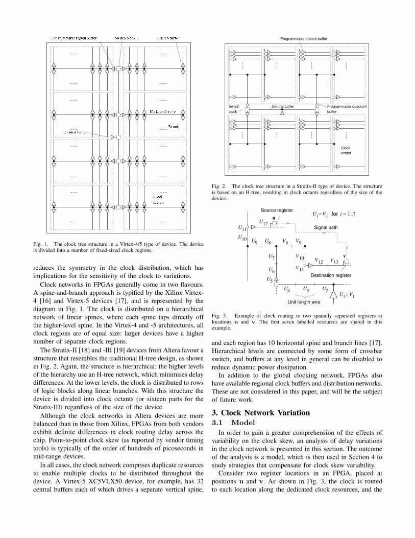
Fig. 1. The clock tree structure in a Virtex-4/5 type of device. The deviceis divided into a number of fixed-sized clock regions.
reduces the symmetry in the clock distribution, which hasimplications for the sensitivity of the clock to variations.
Clock networks in FPGAs generally come in two flavours.A spine-and-branch approach is typified by the Xilinx Virtex-4 [16] and Virtex-5 devices [17], and is represented by thediagram in Fig. 1. The clock is distributed on a hierarchicalnetwork of linear spines, where each spine taps directly offthe higher-level spine. In the Virtex-4 and -5 architectures, allclock regions are of equal size: larger devices have a highernumber of separate clock regions.
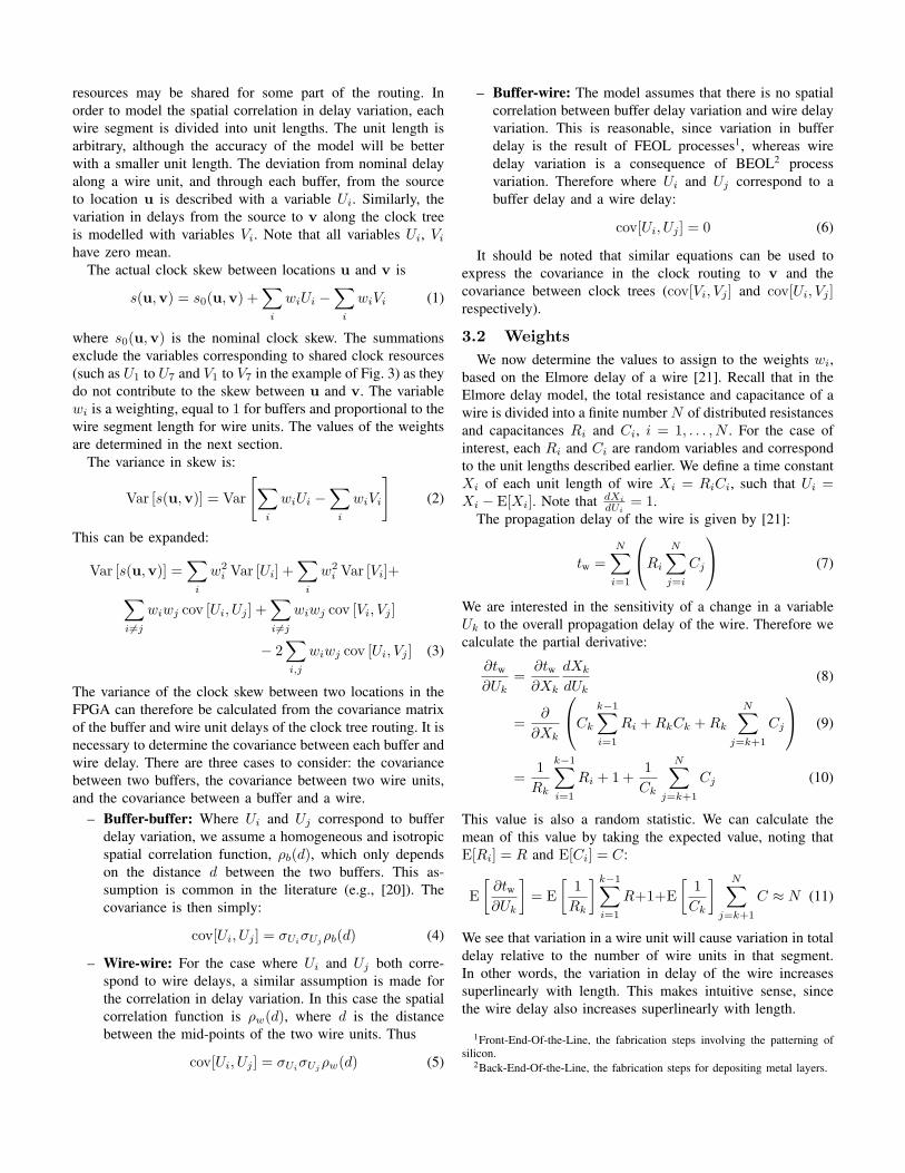
The Stratix-II [18] and -III [19] devices from Altera favour astructure that resembles the traditional H-tree design, as shownin Fig. 2. Again, the structure is hierarchical: the higher levelsof the hierarchy use an H-tree network, which minimises delaydifferences. At the lower levels, the clock is distributed to rowsof logic blocks along linear branches. With this structure thedevice is divided into clock octants (or sixteen parts for theStratix-III) regardless of the size of the device.
Although the clock networks in Altera devices are morebalanced than in those from Xilinx, FPGAs from both vendorsexhibit definite differences in clock routing delay across thechip. Point-to-point clock skew (as reported by vendor timingtools) is typically of the order of hundreds of picoseconds inmid-range devices.
In all cases, the clock network comprises duplicate resourcesto enable multiple clocks to be distributed throughout thedevice. A Virtex-5 XC5VLX50 device, for example, has 32central buffers each of which drives a separate vertical spine,
Programmable branch buffer
Switch
block
Central buffer Programmable quadrant
buffer
octant
Clock
Fig. 2. The clock tree structure in a Stratix-II type of device. The structureis based on an H-tree, resulting in clock octants regardless of the size of thedevice.
U8
U9
U10
V8V
9
V10
U2
U3
U4
U1V
1=
u
V13
V12
U12
U7
U6
U5
V11
U11
=Vi
Ui
= 1..7for i
v
Source register
Destination register
Unit length wire
Signal path
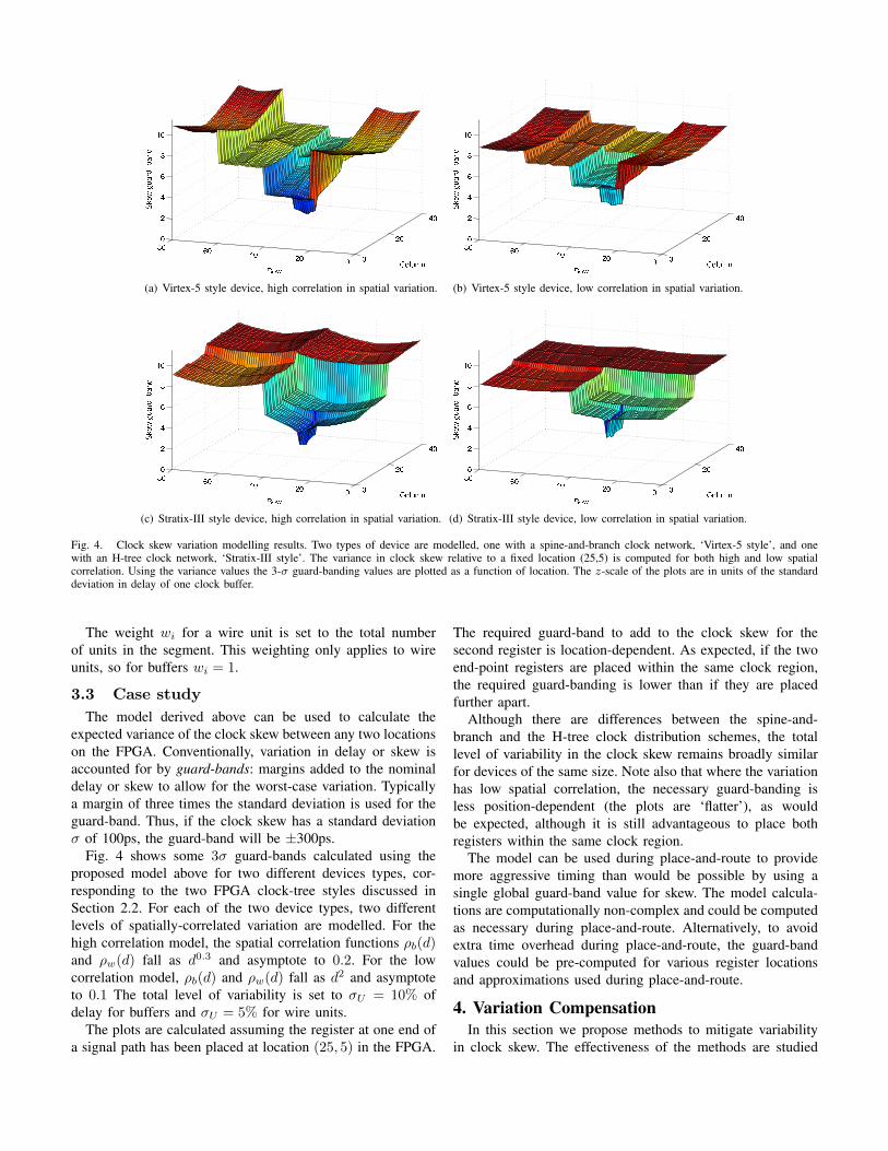
Fig. 3. Example of clock routing to two spatially separated registers atlocations u and v. The first seven labelled resources are shared in thisexample.
and each region has 10 horizontal spine and branch lines [17].Hierarchical levels are connected by some form of crossbarswitch, and buffers at any level in general can be disabled toreduce dynamic power dissipation.
In addition to the global clocking network, FPGAs alsohave available regional clock buffers and distribution networks.These are not considered in this paper, and will be the subjectof future work.
3. Clock Network Variation3.1 Model
In order to gain a greater comprehension of the effects ofvariability on the clock skew, an analysis of delay variationsin the clock network is presented in this section. The outcomeof the analysis is a model, which is then used in Section 4 tostudy strategies that compensate for clock skew variability.
Consider two register locations in an FPGA, placed atpositions u and v. As shown in Fig. 3, the clock is routedto each location along the dedicated clock resources, and the
resources may be shared for some part of the routing. Inorder to model the spatial correlation in delay variation, eachwire segment is divided into unit lengths. The unit length isarbitrary, although the accuracy of the model will be betterwith a smaller unit length. The deviation from nominal delayalong a wire unit, and through each buffer, from the sourceto location u is described with a variable Ui. Similarly, thevariation in delays from the source to v along the clock treeis modelled with variables Vi. Note that all variables Ui, Vi
have zero mean.The actual clock skew between locations u and v is
s(u,v) = s0(u,v) +∑
i
wiUi −∑
i
wiVi (1)
where s0(u,v) is the nominal clock skew. The summationsexclude the variables corresponding to shared clock resources(such as U1 to U7 and V1 to V7 in the example of Fig. 3) as theydo not contribute to the skew between u and v. The variablewi is a weighting, equal to 1 for buffers and proportional to thewire segment length for wire units. The values of the weightsare determined in the next section.
The variance in skew is:
Var [s(u,v)] = Var
[∑i
wiUi −∑
i
wiVi
](2)
This can be expanded:
Var [s(u,v)] =∑
i
w2i Var [Ui] +
∑i
w2i Var [Vi]+∑
i 6=j
wiwj cov [Ui, Uj ] +∑i 6=j
wiwj cov [Vi, Vj ]
− 2∑i,j
wiwj cov [Ui, Vj ] (3)
The variance of the clock skew between two locations in theFPGA can therefore be calculated from the covariance matrixof the buffer and wire unit delays of the clock tree routing. It isnecessary to determine the covariance between each buffer andwire delay. There are three cases to consider: the covariancebetween two buffers, the covariance between two wire units,and the covariance between a buffer and a wire.
– Buffer-buffer: Where Ui and Uj correspond to bufferdelay variation, we assume a homogeneous and isotropicspatial correlation function, ρb(d), which only dependson the distance d between the two buffers. This as-sumption is common in the literature (e.g., [20]). Thecovariance is then simply:
cov[Ui, Uj ] = σUiσUj ρb(d) (4)
– Wire-wire: For the case where Ui and Uj both corre-spond to wire delays, a similar assumption is made forthe correlation in delay variation. In this case the spatialcorrelation function is ρw(d), where d is the distancebetween the mid-points of the two wire units. Thus
cov[Ui, Uj ] = σUiσUj
ρw(d) (5)
– Buffer-wire: The model assumes that there is no spatialcorrelation between buffer delay variation and wire delayvariation. This is reasonable, since variation in bufferdelay is the result of FEOL processes1, whereas wiredelay variation is a consequence of BEOL2 processvariation. Therefore where Ui and Uj correspond to abuffer delay and a wire delay:
cov[Ui, Uj ] = 0 (6)
It should be noted that similar equations can be used toexpress the covariance in the clock routing to v and thecovariance between clock trees (cov[Vi, Vj ] and cov[Ui, Vj ]respectively).
3.2 WeightsWe now determine the values to assign to the weights wi,
based on the Elmore delay of a wire [21]. Recall that in theElmore delay model, the total resistance and capacitance of awire is divided into a finite number N of distributed resistancesand capacitances Ri and Ci, i = 1, . . . , N . For the case ofinterest, each Ri and Ci are random variables and correspondto the unit lengths described earlier. We define a time constantXi of each unit length of wire Xi = RiCi, such that Ui =Xi − E[Xi]. Note that dXi
dUi= 1.
The propagation delay of the wire is given by [21]:
tw =N∑
i=1
Ri
N∑j=i
Cj
(7)
We are interested in the sensitivity of a change in a variableUk to the overall propagation delay of the wire. Therefore wecalculate the partial derivative:
∂tw
∂Uk=
∂tw
∂Xk
dXk
dUk(8)
=∂
∂Xk
Ck
k−1∑i=1
Ri + RkCk + Rk
N∑j=k+1
Cj
(9)
=1
Rk
k−1∑i=1
Ri + 1 +1
Ck
N∑j=k+1
Cj (10)
This value is also a random statistic. We can calculate themean of this value by taking the expected value, noting thatE[Ri] = R and E[Ci] = C:
E[
∂tw
∂Uk
]= E
[1
Rk
] k−1∑i=1
R+1+E[
1Ck
] N∑j=k+1
C ≈ N (11)
We see that variation in a wire unit will cause variation in totaldelay relative to the number of wire units in that segment.In other words, the variation in delay of the wire increasessuperlinearly with length. This makes intuitive sense, sincethe wire delay also increases superlinearly with length.
1Front-End-Of-the-Line, the fabrication steps involving the patterning ofsilicon.
2Back-End-Of-the-Line, the fabrication steps for depositing metal layers.
(a) Virtex-5 style device, high correlation in spatial variation. (b) Virtex-5 style device, low correlation in spatial variation.
(c) Stratix-III style device, high correlation in spatial variation. (d) Stratix-III style device, low correlation in spatial variation.
Fig. 4. Clock skew variation modelling results. Two types of device are modelled, one with a spine-and-branch clock network, ‘Virtex-5 style’, and onewith an H-tree clock network, ‘Stratix-III style’. The variance in clock skew relative to a fixed location (25,5) is computed for both high and low spatialcorrelation. Using the variance values the 3-σ guard-banding values are plotted as a function of location. The z-scale of the plots are in units of the standarddeviation in delay of one clock buffer.
The weight wi for a wire unit is set to the total numberof units in the segment. This weighting only applies to wireunits, so for buffers wi = 1.
3.3 Case studyThe model derived above can be used to calculate the
expected variance of the clock skew between any two locationson the FPGA. Conventionally, variation in delay or skew isaccounted for by guard-bands: margins added to the nominaldelay or skew to allow for the worst-case variation. Typicallya margin of three times the standard deviation is used for theguard-band. Thus, if the clock skew has a standard deviationσ of 100ps, the guard-band will be ±300ps.
Fig. 4 shows some 3σ guard-bands calculated using theproposed model above for two different devices types, cor-responding to the two FPGA clock-tree styles discussed inSection 2.2. For each of the two device types, two differentlevels of spatially-correlated variation are modelled. For thehigh correlation model, the spatial correlation functions ρb(d)and ρw(d) fall as d0.3 and asymptote to 0.2. For the lowcorrelation model, ρb(d) and ρw(d) fall as d2 and asymptoteto 0.1 The total level of variability is set to σU = 10% ofdelay for buffers and σU = 5% for wire units.
The plots are calculated assuming the register at one end ofa signal path has been placed at location (25, 5) in the FPGA.
The required guard-band to add to the clock skew for thesecond register is location-dependent. As expected, if the twoend-point registers are placed within the same clock region,the required guard-banding is lower than if they are placedfurther apart.
Although there are differences between the spine-and-branch and the H-tree clock distribution schemes, the totallevel of variability in the clock skew remains broadly similarfor devices of the same size. Note also that where the variationhas low spatial correlation, the necessary guard-banding isless position-dependent (the plots are ‘flatter’), as wouldbe expected, although it is still advantageous to place bothregisters within the same clock region.
The model can be used during place-and-route to providemore aggressive timing than would be possible by using asingle global guard-band value for skew. The model calcula-tions are computationally non-complex and could be computedas necessary during place-and-route. Alternatively, to avoidextra time overhead during place-and-route, the guard-bandvalues could be pre-computed for various register locationsand approximations used during place-and-route.
4. Variation CompensationIn this section we propose methods to mitigate variability
in clock skew. The effectiveness of the methods are studied
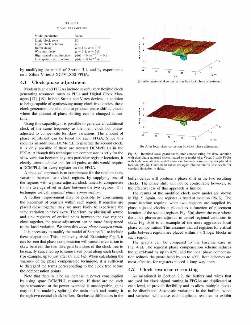
TABLE IMODEL PARAMETERS
Model parameter ValueLogic block rows 80Logic block columns 40Buffer delay µ = 1.0, σ = 10%Wire unit delay µ = 0.1, σ = 5%High spatial corr. function ρ(d) = 0.3d−0.3 + 0.2Low spatial corr. function ρ(d) = 0.1d−2 + 0.1
by modifying the model of Section 3.1, and by experimentson a Xilinx Virtex-5 XC5VLX50 FPGA.
4.1 Clock phase adjustmentModern high-end FPGAs include several very flexible clock
generating resources, such as PLLs and Digital Clock Man-agers [17], [19]. In both Stratix and Virtex devices, in additionto being capable of synthesizing many clock frequencies, theseclock generators are also able to produce phase-shifted clockswhere the amount of phase-shifting can be changed at run-time.
Using this capability, it is possible to generate an additionalclock of the same frequency as the main clock but phase-adjusted to compensate for skew variations. The amount ofphase adjustment can be tuned for each FPGA. Since thisrequires an additional DCM/PLL to generate the second clock,it is only possible if there are unused DCMs/PLLs in theFPGA. Although this technique can compensate exactly for theskew variation between any two particular register locations, itclearly cannot achieve this for all paths, as this would requirea DCM/PLL for every register on the FPGA.
A practical approach is to compensate for the random skewvariation between two clock regions, by supplying one ofthe regions with a phase-adjusted clock tuned to compensatefor the average offset in skew between the two regions. Thistechnique we call regional phase compensation.
A further improvement may be possible by constrainingthe placement of registers within each region. If registers areplaced close together they are more likely to experience thesame variation in clock skew. Therefore, by placing all sourceand sink registers of critical paths between the two regionsclose together, the phase adjustment can be more finely tunedto the local variation. We term this local phase compensation.
It is necessary to modify the model of Section 3.1 to includethese adaptations. This is relatively trivial. Examining Fig. 3, itcan be seen that phase compensation will cause the variation inskew between the two divergent branches of the clock tree tobe exactly cancelled up to some fixed point along each branch(for example, up to just after U9 and V9). When calculating thevariance of the phase compensated technique, it is sufficientto disregard the terms corresponding to the clock tree beforethe compensation points.
Note that there will be an increase in power consumptionby using spare DCM/PLL resources. If there are no suchspare resources, or the power overhead is unacceptable, gainsmay still be made by splitting the main clock and routing itthrough two central clock buffers. Stochastic differences in the
(a) After regional skew correction by clock phase adjustment.
(b) After local skew correction by clock phase adjustment.
Fig. 5. Required skew guard-bands after compensating for skew variationwith dual phase-adjusted clocks, based on a model of a Virtex-5 style FPGAwith high correlation in spatial variation. Assumes a source register placed atlocation (25, 5). Guard-band values are again plotted relative to clock bufferstandard deviation in delay.
buffer delays will produce a phase shift in the two resultingclocks. The phase shift will not be controllable however, sothe effectiveness of this approach is limited.
The results of the modified clock skew model are shownin Fig. 5. Again, one register is fixed at location (25, 5). Theguard-banding required when two registers are supplied byphase-adjusted clocks is plotted as a function of placementlocation of the second register. Fig. 5(a) shows the case wherethe clock phases are adjusted to cancel regional variations inskew. Fig. 5(b) is an example of the more aggressive localphase compensation. This assumes that all registers for criticalpaths between regions are placed within 3× 3 logic blocks ineach region.
The graphs can be compared to the baseline case inFig. 4(a). The regional phase compensation scheme reducesthe guard-band by up to 42%, and the local phase compensa-tion reduces the guard-band by up to 49%. Both schemes aremost effective for registers placed a long way apart.
4.2 Clock resource re-routingAs mentioned in Section 2.2, the buffers and wires that
are used for clock signal routing in FPGAs are duplicated ateach level, to provide flexibility and to allow multiple clocksto be distributed. Stochastic variations in the buffers, wiresand switches will cause each duplicate resource to exhibit

different delays. It is possible to use these differences, givena particular FPGA and one clock net of interest, by selectinga clock routing which gives the most optimal clock skew.
As an example, consider the Virtex-5 FPGA from Xilinx. Inthis device there are 10 nominally identical horizontal clockspines per region. At each register there is a multiplexer whichdetermines which clock spine is connected to the clock inputof the register. The clock signal can be routed on all 10 clocklines simultaneously, and the ‘best’ signal selected at eachregister by reconfiguring the multiplexer.
The ‘best’ or most optimal signal may be the signal with theclosest to nominal skew. Alternatively, a clock signal with adeviation in skew could be selected to compensate for reducedslack caused by path delay variations.
Nominal skew objective: By choosing the signal with theclosest-to-nominal skew, the skew variance will be reducedand therefore the required guard-band will also be smaller. Toinclude this in the model, we need to quantify the effect ofselection on the skew variance. Firstly, note that the duplicatedclock resources are physically close together, so will exhibitthe same correlated delay variation. The difference in skew ofN duplicated resources is therefore a stochastic quantity ofzero mean, which we will denote by the random variable Xi,i = 1, . . . , N .
Assuming that Xi is approximately normally distributedwith variance σ2, its probability density can be described by
P(−x < Xi < x) = erf(
x√2σ
)(12)
where erf(x) is the error function. Let us label the value ofXi which is closest to zero by Y . It is straightforward to showthat:
fY (x) = P(Y = x)
=N√2πσ
exp(−x2
2σ2
) [1− erf
(|x|√2σ
)]N−1
(13)
The variance of Y is defined as Var[Y ] =∫∞−∞ x2fY (x)dx
which, while not possible to solve analytically, can be com-puted numerically. For N = 10, the variance Var[Y ] =0.024704× σ2.
This is applied to the model of (3) by scaling the varianceterms corresponding to the duplicated resources. The covari-ance terms remain the same.
Positive skew objective: For a given register, instead ofselecting the clock routing that gives the most nominal skew,one may choose to select the routing that gives the mostpositive skew. This will yield the most slack for paths thatend at that register, although at the expense of slack for pathsoriginating at the register. In this case, we select the maximumvalue of Xi, which is the order statistic X〈N〉. The variancevalues in the model of (3) will be replaced by Var[X〈N〉], andthe guard-band will be reduced by E[X〈N〉]. Order statisticshave been extensively studied; mean and variance tables arereadily available, such as in [22].
(a) Nominal skew objective.
(b) Most positive skew objective.
Fig. 6. Guard-bands after compensating for skew by clock phase adjustmentsand clock re-routing, for a high amount of spatially correlated delay.
Results from the modified models for the clock resource re-routing strategies are plotted in Fig. 6. Both models assumethat regional differences in phase are compensated for by theclock phase adjustment described above, and then the best of10 available regional clock trees are used to route the clocksignal. The graphs should therefore be compared to Fig. 5(a).
By choosing the resources which give the nearest to nominalskew, the guard-band can be reduced by an additional 10%to 40% over regional phase compensation alone. The benefitis greatest when the two registers are placed close together.The most positive skew objective yields improvements of 30%to 90% additional reduction in guard-band compared withregional phase compensation.
The results in Fig. 5(a) and Fig. 5(b) are based on a highlevel of spatial correlation. The model has also been usedto investigate the situation where the delay variation is morestochastic. The results are broadly similar. The guard-bandresult for the clock resource re-routing for nominal skew isshown in Fig. 7 as an example. Compared to the highlycorrelated variation case of Fig. 6(a) the method offers lessof an improvement for closely-spaced registers, and overallthe guard-band has less locational dependence, as would beexpected.
4.3 Experimental resultsIn order to validate the feasibility of the proposed skew
variability compensation techniques, experiments have been

Fig. 7. Guard-band after compensating for skew by clock phase adjustmentsand clock re-routing. The model assumes low spatial correlation in delayvariation and the clock re-routing targets nominal skew.
4 possible central
buffer locations
’Down’ paths
x16
’Up’ paths
x16
4
9
9 possible regional buffers
Phase
adjust
Clock
generation
Launch
Test path Test path
Launch
Capture
Capture
Fig. 8. A simplified diagram of the test circuitry used in the Virtex-5experiment. Two clock regions (‘top’ and ‘bottom’) are supplied with separateclocks. The phase offset between the clocks can be adjusted dynamically. Atotal of 32 paths connect the two regions, 16 in either direction.
performed on a Xilinx Virtex-5 XC5VLX50-1 FPGA. Theseare designed to determine whether or not it is possible tochange the clock phase for a region to compensate for skewvariation, and if different parallel clock resources do actuallyexhibit different delays.
A simplified diagram of the test circuitry used is shown inFig. 8. Two clock regions in the FPGA were supplied withseparate clocks of the same frequency, where the phase offsetbetween the two clocks can be adjusted dynamically. Thephase adjustment was achieved using the Virtex embeddedDigital Clock Managers [17]. Thirty-two paths were placedand routed in the FPGA between the two clock regions, 16in each direction. Paths originating in the lower of the tworegions are termed ‘up paths’, the others ‘down paths’.
The ‘observable delay’ of each path was able to be ac-curately measured using the method reported in [3]. Theobserved delay of the path in reality is the sum of the pathpropagation delay and the clock skew between the start and theend registers of the path. An additional 192 paths were placedand routed in other regions of the FPGA, and were used forcalibrating the measurements for environmental changes.
The experiment involved measuring the observable delayof the 32 test paths for different clock phase offsets, andwhen different clock resources were used to route the clock of
Fig. 9. Empirical measurements and post-calibration values of observedpath delay for all 32 paths (16 ‘up’ and 16 ‘down’) under test. Each path ismeasured 36 times, each time with a different combination of central bufferlocation and regional clock routing.
the top-most region. Since the paths under test are invariant,any change in observed delay is therefore actually caused bychanges in clock skew.
The raw measured path delays for all 36 combinations ofclock routing are plotted in the left half of Fig. 9. It can beseen that changing the resources the clock is routed on causes achange in measured delay of up to ±50ps. This is significantwhen compared to the variation in LUT delay, which has astandard deviation of approximately 11ps in this device [4].The mean measured path delay is 3705ps. Note that there isa difference in the ensemble measurements of the ‘up’ paths(3807ps) compared to the ‘down’ paths (3603ps). There arealso differences in delays between paths within the ‘up’ groupand within the ‘down’ group. These differences are partiallydue to process variability and partially due to differences inthe placement and routing of each path.
Since we are interested in compensating for clock skewvariation, it is necessary to calibrate the initial data-set toproduce a set of values where the the effect of other sources ofvariation in the delay have been removed. The measurementswere first calibrated to remove expected differences in delayusing the path and skew timing reported by the vendor timingtools. The resulting values for the delay of each path were thenshifted towards the mean to counteract the variance introducedby the LUT in each path. The resulting post-calibrated values,plotted in the right half of Fig. 9, are somewhat artificial butrealistic.
The effect of different experiments are summarised inFig. 10. The graph shows the timing offset (degradation)of the slowest path for a given test, relative to the case ofnil variation. Nil variation is estimated as the mean of allcalibrated delays. In order to gain an insight into how thedegree of connectivity between regions affects the results,three bars are shown in each experiment: the case where theregions are connected by just one path in each direction, aswell as for four paths and sixteen paths. To give a meaningfulsense of scale to the results, standard deviations of LUT delay,σL, are also plotted on the graph.
Using the initial assignment of clock resources and no phase
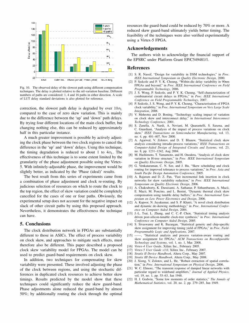
Fig. 10. The observed delay of the slowest path using different compensationtechniques. The delay is plotted relative to the nil-variation baseline. Differentnumbers of paths are considered: 1, 4 and 16 paths in either direction. A scaleof LUT delay standard deviations is also plotted for reference.
correction, the slowest path delay is degraded by over 10σLcompared to the case of zero skew variation. This is mainlydue to the difference between the ‘up’ and ‘down’ path delays.By trying four different locations of the main clock buffer, butchanging nothing else, this can be reduced by approximatelyhalf in this particular instance.
A much greater improvement is possible by actively adjust-ing the clock phase between the two clock regions to cancel thedifference in the ‘up’ and ‘down’ delays. Using this technique,the timing degradation is reduced to about 1 to 4σL. Theeffectiveness of this technique is to some extent limited by thegranularity of the phase adjustment possible using the Virtex-5. With infinitely-adjustable phase, the improvement would beslightly better, as indicated by the ‘Phase (ideal)’ results.
The best result from this series of experiments came froma combination of phase adjustment and clock re-routing. Byjudicious selection of resources on which to route the clock tothe top region, the effect of skew variation could be completelycancelled for the cases of one or four paths. Obviously, theexperimental setup does not account for the negative impact onslack of other circuit paths by using this proposed approach.Nevertheless, it demonstrates the effectiveness the techniquecan have.
5. ConclusionsThe clock distribution network in FPGAs are substantially
different to those in ASICs. The effect of process variabilityon clock skew, and approaches to mitigate such effects, musttherefore also be different. This paper described a proposedclock skew variability model for FPGAs. The model can beused to predict guard-band requirements on clock skew.
In addition, two techniques for compensating for skewvariability were presented. These involved adjusting the phaseof the clock between regions, and using the stochastic dif-ferences in duplicated clock resources to achieve better skewtimings. Results predicted by the model show that thesetechniques could significantly reduce the skew guard-band.Phase adjustments alone reduced the guard-band by almost50%; by additionally routing the clock through the optimal
resources the guard-band could be reduced by 70% or more. Areduced skew guard-band ultimately yields better timing. Thefeasibility of the techniques were also verified experimentallyusing a Virtex-5 FPGA.
AcknowledgementsThe authors wish to acknowledge the financial support of
the EPSRC under Platform Grant EP/C549481/1.
References[1] S. R. Nassif, “Design for variability in DSM technologies,” in Proc.
IEEE International Symposium on Quality Electronic Design, 2000.[2] P. Sedcole and P. Y. K. Cheung, “Within-die delay variability in 90nm
FPGAs and beyond,” in Proc. IEEE International Conference on FieldProgrammable Technology, 2006.
[3] J. S. Wong, P. Sedcole, and P. Y. K. Cheung, “Self-characterization ofcombinatorial circuit delays in FPGAs,” in Proc. IEEE InternationalConference on Field Programmable Technology, 2007.
[4] P. Sedcole, J. S. Wong, and P. Y. K. Cheung, “Characterisation of FPGAclock variability,” in Proc. International Symposium on Very Large ScaleIntegration, 2008.
[5] V. Mehrotra and D. Boning, “Technology scaling impact of variationon clock skew and interconnect delay,” in International InterconnectTechnology Conference, 2001.
[6] S. Zanella, A. Nardi, A. Neviani, M. Quarantelli, S. Saxena, andC. Guardiani, “Analysis of the impact of process variations on clockskew,” IEEE Transactions on Semiconductor Manufacturing, vol. 13,no. 4, pp. 401–407, Nov 2000.
[7] A. Agarwal, V. Zolotov, and D. T. Blaauw, “Statistical clock skewanalysis considering intradie-process variations,” IEEE Transactions onComputer-Aided Design of Integrated Circuits and Systems, vol. 23,no. 8, pp. 1231–1242, Aug 2004.
[8] M. Hashimoto, T. Yamamoto, and H. Onodera, “Analysis of clock skewvariation in H-tree structure,” in Proc. IEEE International Symposiumon Quality Electronic Design, 2005.
[9] G. Venkataraman, C. N. Sze, and J. Hu, “Skew scheduling and clockrouting for improved tolerance to process variations,” in Proc. Asia andSouth Pacific Design Automation Conference, 2005.
[10] A. Rajaram and D. Z. Pan, “Fast incremental link insertion in clocknetworks for skew variability reduction,” in Proc. IEEE InternationalSymposium on Quality Electronic Design, 2006.
[11] A. Chakraborty, K. Duraisami, A. Sathanur, P. Sithambaram, A. Macii,E. Macii, M. Poncino, and L. Benini, “Dynamic thermal clock skewcompensation using tunable delay buffers,” in Proc. International Sym-posium on Low Power Electronics and Design, 2006.
[12] A. Kapoor, N. Jayakumar, and S. P. Khatri, “A novel clock distributionand dynamic de-skewing methodology,” in Proc. International Confer-ence on Computer Aided Design, 2004.
[13] J.-L. Tsai, L. Zhang, and C. C.-P. Chen, “Statistical timing analysisdriven post-silicon-tunable clock-tree synthesis,” in Proc. InternationalConference on Computer Aided Design, 2005.
[14] S. Sivaswamy and K. Bazargan, “Statistical generic and chip-specificskew assignment for improving timing yield of FPGAs,” in Proc. Field-Programmable Logic and Applications, 2007.
[15] ——, “Statistical analysis and process variation-aware routing andskew assignment for FPGAs,” ACM Transactions on ReconfigurableTechnology and Systems, vol. 1, no. 1, Mar. 2008.
[16] Virtex-4 User Guide, Xilinx Inc., February 2005.[17] Virtex-5 User Guide v3.0, Xilinx Inc., February 2007.[18] Stratix II Device Handbook, Altera Corp., May 2007.[19] Stratix III Device Handbook, Altera Corp., May 2008.[20] J. Xiong, V. Zolotov, and L. He, “Robust extraction of spatial correla-
tion,” in Proc. International Symposium on Physical Design, 2006.[21] W. C. Elmore, “The transient response of damped linear networks with
particular regard to wideband amplifiers,” Journal of Applied Physics,vol. 19, no. 1, pp. 55–63, Jan 1948.
[22] H. J. Godwin, “Some low moments of order statistics,” The Annals ofMathematical Statistics, vol. 20, no. 2, pp. 279–285, Jun 1949.