modeling of transistor self-heating for circuit simulation
TRANSCRIPT

MODELING OF TRANSISTOR SELF-HEATINGFOR CIRCUIT SIMULATION
By
DAVID T. ZWEIDINGER
A DISSERTATION PRESENTED TO THE GRADUATE SCHOOLOF THE UNIVERSITY OF FLORIDA IN PARTIAL FULFILLMENT
OF THE REQUIREMENTS FOR THE DEGREE OFDOCTOR OF PHILOSOPHY
UNIVERSITY OF FLORIDA
1997

ACKNOWLEDGMENTS
I would like to thank Dr. Robert Fox for his patience, the
Semiconductor Research Corporation for the financial support, the many
people of Harris Semiconductor for their assistance and encouragement,
Jon Brodsky for his long hours simulating heat-flow, and finally my
parents for doing it all before me and reminding me why it was worth the
work.
ii

TABLE OF CONTENTS
page
ACKNOWLEDGMENTS ii
ABSTRACT v
CHAPTERS
1 INTRODUCTION 1
2 BACKGROUND 4
The SPICE Gummel-Poon Model 4Thermal Impedance Modeling 6Self-Heating Models 10
3 MODELING FOR CIRCUIT SIMULATION 15
An Overview of SPICE 15Formulation of the Self-Heating Model 17Implicit Temperature Approach 18
Thermal Impedance Modeling 19The DC Solution 20AC Modifications 27Advantages and Limitations 28
Explicit Temperature Node Approach 29The DC Solution 29Implementation Options 32SPICE Code Modification
' '
'
' 34Advantages and Limitations 39
Convergence 40
4 SELF-HEATING IN CIRCUITS 44
Self-Heating Effects 44Simulation Examples 4gConvergence Comparison 57
iii

iv
5 MEASUREMENT OF MODEL PARAMETERS 60
Measurement of the Thermal Impedance 60Temperature Coefficient Measurement 62
Thermal Impedance Measurement 67
Thermal Impedance Model and SPICE 72Self-heating and Model Parameter Extraction 75
6 SELF-HEATING FOR SOISPICE 83
Self-Heating Implementation 85The SOI MOSFET Model 85Specifying Self-Heating 86Computing the Derivatives 87Computing the Power Dissipation 88Local Temperature Update of Parameters 88Loading the Jacobian 90Convergence Issues 92
Initial Simulation Results 93Conclusion 97
7 CONCLUSION 98
APPENDLX A 101
APPENDIX B 115
APPENDLX C 127
APPENDIX D 140
BIBLIOGRAPHY 148
BIOGRAPHICAL SKETCH 153

Abstract of Dissertation Presented to the Graduate Schoolof the University of Florida in Partial Fulfillment of theRequirements for the Degree of Doctor of Philosophy
MODELING OF TRANSISTOR SELF-HEATINGFOR CIRCUIT SIMULATION
By
David T. Zweidinger
August 1997
Chairman: Robert M. FoxMajor Department: Electrical and Computer Engineering
Semiconductor devices consume power during operation. This power
is dissipated mostly in the form of heat that increases the temperature of
the device. This effect is known as self-heating. For bipolar transistors,
BJTs, and silicon-on-insulator metal-oxide-semiconductor field-effect
transistors, SOI MOSFETs, self-heating can significantly change device
performance. Circuit designers need an easy way to quantify the
performance changes from self-heating, within the compact models used
in today's circuit simulators.
A historical review of other attempts at modeling self-heating in
circuit simulators is shown. Two approaches to including self-heating
effects for bipolar transistors in the popular circuit simulator SPICE are
presented. One approach uses an implicit temperature and transcendental
equations to correct for self-heating in the device model. The other
v

approach uses an explicit temperature and an electrical subcircuit
analogy for power generation and thermal dissipation to model self-
heating. Techniques for assessing self-heating effects in hand calculations
are shown, and example simulations with self-heating in common dc, ac,
and transient circuits are shown. Reduced amplifier gain and thermal
mismatching are common self-heating effects.
A new method for extracting the thermal impedance of bipolar
transistors is derived, and results are shown for transistors of several
different geometries. The effects of self-heating on the extraction of the
Gummel-Poon model parameters are explored using long-time
measurements and the modified SPICE in the optimization process.
The implementation of self-heating in the physics-based SOISPICE
model for SOI MOSFETs is shown. Common circuit examples are
simulated showing the effects of self-heating. For analog circuits, the
negative temperature coefficient of drain current can cause problems for
biasing and amplifier gains. For digital circuits, self-heating is a function
of frequency and is not significant.
vi
CHAPTER 1
INTRODUCTION
In present circuit simulators, temperature is primarily modeled
globally. Only a single temperature is used for all of the circuit elements,
and the circuit is simulated isothermally at that temperature. This
approach ignores self-heating, the local increase in temperature from the
power dissipation of a device. The operating point of a device defines its
power generation, and the geometries and materials affect how the power
is dissipated as heat. The isothermal simplification is inaccurate
considering that most circuits have many elements of different
geometries, operating under different bias, and dissipating different
amounts of power. The result is a performance change of the circuit
because of all of elements operating at different temperatures. These
performance changes from self-heating are significant for many circuits.
Semiconductor devices are especially sensitive to their operating
temperature. One device that is particularly sensitive is the bipolar
junction transistor (BJT). In BJTs the dominant sensitivity arises from
the exponential dependence of the carrier concentration on temperature.
Only a few degrees Kelvin of temperature change will cause significant
changes in the carrier concentration. The BJT terminal currents are a
function of the carrier concentration, and hence are greatly affected by
1

2
small temperature changes. Some temperature dependent mechanisms
that are weaker than the carrier concentration are the carrier mobility
and recombination lifetimes which become significant when large
temperature changes occur on the order of tens of degrees Kelvin. These
two mechanisms are important to silicon-on-insulator metal-oxide-silicon
field-effect transistors, SOI MOSFETs. Self-heating can cause failure of
heterojunction bipolar transistors (HBT) where the large negative
temperature coefficients cause currents to drop to zero in relatively low-
power operation [Gao89]. Including these effects in the compact BJT and
SOI MOSFET models used in circuit simulation is important for
improving accuracy in some circuits.
The importance of self-heating has become more evident with
changes in technology. The continued shrinking of geometries, and the
resulting increase in current densities and restriction of heat flow, tend to
increase the thermal impedance and raise device operating temperatures.
The thermal impedance is the temperature increase for a given power
dissipation. The trend toward the use of silicon dioxide, Si02 , for isolation
makes self-heating more important, because the decreased thermal
conductivity of Si02 compared to silicon creates a barrier to heat flow and
greatly increases the thermal impedance of the device.
Finite element-based simulators are available that can simulate a
BJT under dc and ac conditions with self-heating [Lia94], but these are
extremely slow for analysis and design of circuits with multiple devices.

3
What circuit designers need is a compact modeling simulator that includes
self-heating. SPICE, with its Gummel-Poon model, is a popular circuit
simulator. The temperature dependencies of all the parameters are
implemented in the code for simulation of circuits at different global
temperatures. The goal is to implement self-heating in the model by
incorporating the temperature dependencies and the device thermal
impedance and power dissipation to allow each device to be simulated at
its own local temperature.
The following chapters are organized to give a understanding of the
motivations for this work and the solutions reached for incorporating self-
heating into circuit simulation. Chapter Two a historical view of thermal
impedance modeling and self-heating simulation. Chapter Three describes
two ways to incorporate self-heating into SPICE. Chapter Four focuses on
circuit analysis in the presence of self-heating and shows some example
simulations. Chapter Five shows a new extraction method for measuring
thermal parameters of BJTs, in particular the thermal impedance. The
effects of self-heating on model parameter extraction are also examined.
Chapter Six shows the implementation of a self-heating model for SOI
MOSFETs, with some simulation examples included. Finally, Chapter
Seven summarizes the information and insights presented.

CHAPTER 2BACKGROUND
This chapter presents an overview of previous work in modeling
self-heating. First, the BJT device model equations used as the framework
for self-heating simulation are reviewed. Following this is an investigation
of thermal impedance modeling. Finally, an examination of previous
attempts to model self-heating in BJTs will show the need for
improvement.
The SPICE Gummel-Poon Model
The dominant model for use in simulating bipolar transistors in
circuits was introduced in 1970 [Gum70]. This integral charge-control
model was incorporated into the circuit simulator SPICE, developed at the
University of California at Berkeley. Most circuit simulators in use today
have a core based on SPICE and its Gummel-Poon BJT model. Therefore,
SPICE was the obvious platform for the study of self-heating in BJTs and
circuits. The communication of self-heating modeling is helped by the
common use of SPICE based simulators in industry. What follows is a
short overview of the SPICE Gummel-Poon model that will form the basis
for most of the discussion in the chapters to come.
The following is the Gummel-Poon model for an npn BJT. The base
current (IB ) is composed of four current elements,
4

5
lB " IBF + IBE + IBR + IBC (2.1)
where Igp is the forward diffusion current that results from back-injected holes
across the base-emitter junction, given by
NFVT- 1 (2.2)
where Ig is the saturation current, (3p- is the forward dc current gain, Np is the
forward current emission coefficient, and VT is the thermal voltage. The non-
ideal base-emitter current results from recombination in the quasi-neutral
base, and is given by:
(Vbe
\NEVT
- 1 (2.3)
where IgE is the base-emitter leakage saturation current and NE is the leakage
emission coefficient. Similarly, the dual for the reverse-bias case exists. IBR is
the reverse diffusion current given by:
(VBCNRVT
BR(3R
- 1 (2.4)
where (3R is the reverse dc current gain and NR is the reverse current emission
coefficient. Finally the non-ideal base-collector current is
!BC ~ JSC
nc
NCVT- 1 (2.5)

6
where Igc is the base-collector leakage saturation current and Nq is the
leakage emission coefficient.
The collector current is given by
T - —c QB
NFVT- e
NRVT_IBR _IBC (2.6)
where Qb is the base charge factor that accounts for base-width modulation
and high-injection conditions. The base charge factor is
Qb = T^V17^ (2.7)
where
Q. = Xbc_XbevI
VAF VAR.
(2.8)
and
fVfiE
A
O - -5§
KF
NFVT- 1
(Vbc
A
+Lsc
KR
NRVT- 1 (2.9)
The parameters and are the forward and reverse early voltages, and
Ikf and Irr are the forward and reverse knee currents or corners for beta high
current roll-off.
Thermal Impedance Modeling
As a device heats from its power dissipation, its operating point
shifts causing the power dissipation to change. This circular mechanism
of heating is called thermal feedback. There are several thermal feedback

7
mechanisms in integrated circuits, which can usually be considered
separately [Mei77, Fox91c]. One mechanism is the rise in the overall chip
temperature due to the total power dissipated on the chip. This
temperature rise is controlled by the chip-to-package and package-to-
ambient thermal impedances. This global heating operates over a long
time scale (milliseconds to minutes), and couples all of the devices on a
chip. Global heating can generally be reduced by careful packaging and
heat-sinking, and is accounted for in circuit simulation by simulating at
multiple temperatures. Global heating is important to recognize in
parameter extraction, where long thermal settling times cause the
isothermal assumption to become inaccurate.
For large-area devices, or those dissipating large power, there can be
direct coupling between the heat dissipated in one device and the
temperature of other devices. This mechanism is strongly affected by the
circuit layout. For example, thermal coupling in an operational amplifier
from the output stage back to the input can profoundly affect the circuit's
gain characteristics, although careful layout exploiting symmetry can
mitigate these effects [Fuk76].
Direct heating of a transistor by its own power dissipation cannot be
eliminated through packaging, scaling, or layout. This mechanism can
cause substantial errors in modeling even without high power dissipation.
As shown by Joy and Schlig, for modest power dissipation, the
temperature rise is mostly confined within the transistor itself [Joy70].

8
Thus this effect can be simulated only by allowing each transistor to be
modeled at its own temperature, controlled by its thermal spreading
impedance and power dissipation. The thermal spreading impedance,
which controls the temperature rise, can be predicted from the transistor's
geometry [Lee92, Bro93, and Zwe95b].
The thermal impedance model derived by Fox and Lee [Fox91b] is
the frequency-domain equivalent of the time-domain derivation shown by
Joy and Schlig [Joy70], and is based on the same assumptions. All of the
heat is assumed to be generated uniformly in the rectangular volume of
the collector space-charge region (SCR). The analysis assumes an
adiabatic plane at the surface of the transistor created by an image of the
SCR heat-source placed above the surface. This approach assumes there is
little heat lost through the top of the BJT and the heat is removed
predominately by the conduction of the body of the semiconductor. For
isolation technologies where Si02 is used between devices, this may not be
a good assumption [Dav92, Bro97a]. In the time domain, the response to a
point impulse of heat, measured a distance r away in a uniform medium, is
where K is the thermal conductivity and k is the thermal diffusivity. The
Laplace transform of (2.10) gives the thermal impedance
For s = 0 ,this equation gives the thermal resistance RTH for the point source.
(2.10)
(2.11)

An expression for RpH at any point r' = (x', y', z') in the semiconductor due to
the heat generated in the collector SCR can be derived by integrating Rj^ over
the collector SCR and its image source. For a rectangular vertical BJT the
integral is
R^W.L.D.H.O =^jJ^^ +J^fififf] ,2.12)
where r = J(x - x')2 + (y - y') 2 + (z - z')
2, W and L are the width and length of
the emitter, D is the collector-base junction depth, and H is the SCR width. The
result in (2.12) can be numerically approximated by [Fox91a, Fox91b]:
RTH = -=L (2.13)4nKVWL • f j
• f2
where
f^d.h) = (0.058d + 0.14)h + 0.34d + 0.28, (2.14)
f2(a) = 0.98 + 0.043a - 6.9 • 10"4a 2 + 3.9 • 10"6a3 , (2.15)
d = -^L, (2.16)
Wa = -,a>l, (2.17)
„ =^(VcB^)AqNEp!)
NEPI is the epitaxial doping density in atoms/cm3,VCB is the collector-base
junction voltage and <|>bl is the collector-junction built-in potential. This
expression was found experimentally to approximate RTH well for a wide
10
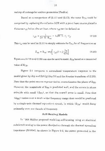
variety of rectangular emitter geometries [Fox91a].
Based on a comparison of (2.11) and (2.13), the same Rth could be
computed by replacing the collector SCR with a point heat source placed a
distance reff below the emitter, where re^-can be denned as
r<« = 2FTri^
= 2^- f '- f2-
(219)
This reft-can be used in (2.11) to simply estimate for Z<th for all frequencies as
(2.20)
Equations (2.19) and (2.20) can also be used to model ZTH based on a measured
value of Rth-
Figure 2-1 compares a normalized temperature response to the
model given by Joy and Schlig [Joy70] and the Fourier transform of (2.20).
Note that the point-source representation overestimates the phase of Zth-
However, the magnitude of Zjh is predicted well, and the errors in phase
coincide with small I
Z
TH I , so that the overall error is small. Note that
I
Z
TH I varies over a much wider frequency range than would be predicted
by a single-pole thermal equivalent circuit, in which I
Z
TH I would decay
primarily over one decade of frequency.
Self-Heating Models
In 1964 Miiller proposed modeling self-heating using an electrical
subcircuit analog to the power dissipation through the thermal spreading
impedance [Mul64]. As shown in Figure 2-2, the power generated in the

11
device flows as a current through an impedance, establishing a potential
equivalent to the change in temperature. Only a single RC pole is shown,
Time (s)
Figure 2-1 Normalized temperature response to a 1 W powerstep for a 7xl0[im npn BJT, using the model in[Joy70] and the inverse Fourier transform of thefrequency response of (2.20) [Fox93b].
Figure 2-2 Example of thermal subcircuit used to model self-
heating.

but electrical networks representing multiple poles could be constructed
to better model the distributed nature of the thermal spreading impedance
[Mul64].
An early attempt at computer simulation of self-heating effects was
done by Latif and Bryant [Lat81]. In this work a simple, single time-
constant, thermal subcircuit was implemented into the Ebers-Moll BJT
model [Ebe54]. They used a linear network solver (WATAND) to simulate
dc and transient effects of second breakdown in power BJTs. Later, this
work was extended to include the more accurate Gummel-Poon model in
the same solver for a study of self-heating effects on current mirrors
[Mun91]. These two works failed to include the effects of self-heating in
the ac analysis.
A single-pole thermal subcircuit was used to model temperature in
SPICE by Vogelsong and Brzezinski [Vog89]. Results from a few circuit
simulations were presented. Again, only dc and transient analysis were
implemented, ignoring the important ac analysis. Their approach to
computing the power dissipation included heat sources other than the
base-collector junction which all have different thermal impedances that
were not modeled. The algorithms they used to implement self-heating are
vague.
In all of the above implementations, values used for the thermal
impedance are empirical. The impedance value used is the one that makes
the simulation fit the data best. This approach can neglect the coupling of

13
self-heating effects to other effects in the device behavior. Most of the
implementations used only a single-pole network which poorly models the
distributed nature of the thermal impedance. Finally, all of the simulators
above require a voltage source in the thermal network to represent the
ambient temperature. Repeating a simulation at a different ambient
temperature would require modification of all of the thermal networks in
the circuit.
The underlying physics of the heat flow either within the transistor
or between transistors is often neglected in the above works. Heat-flow
analysis shows that except for rather high-power transistors, temperature
gradients are mostly confined within the transistor itself [Joy70]. Usually
adjacent devices are thermally coupled through the device-to-chip-to-
package spreading impedances, that have very long time constants, rather
than device-to-device impedances [Lee92]. The heat coupling effects can
usually be ignored. Where the heating of adjacent devices cannot be
ignored is in multi-fingered emitter BJTs and HBTs. The close proximity
of each finger causes a strong thermal coupling. For example, for a three
finger BJT driven with a constant current, the middle finger is heated by
the two outside fingers causing its current to increase and the others to
decrease. This effect can degrade the performance of multi-fingered
emitter devices.
The improved implementation shown in the next chapter includes
dc, transient, and ac analyses. It allows flexibility in formation of the

14
thermal impedance network, so that the self impedance and impedance to
adjacent devices or emitter fingers can be modeled accurately.

CHAPTER 3MODELING FOR CIRCUIT SIMULATION
Because of the deficiencies of previous attempts to include self-
heating in circuit simulation, a more complete self-heating
implementation was needed. The first priority was to create a simulator
that could model the ac effects of self-heating. The frequency domain had
been mostly ignored for analog circuits. The first implementation filled
this void using an implicit local temperature approach. In the implicit
temperature approach the BJT model is reduced to a two-port y-parameter
equivalent model. The y-parameters are then modified by self-heating,
and the modified y-parameters are converted back to the original model
form. Unfortunately, this implementation made transient analysis very
difficult, so another implementation using an explicit temperature and
thermal subcircuit was done. A thermal subcircuit represents the power
dissipation, heat flow, and temperature rise. This requires a thermal
impedance network with some inherent limitations, but does allow
transient analysis, unlike the implicit node approach. Both of these
approaches are described in this chapter.
An Overview of SPICE
To understand the implementations, it is important to understand
first the organization and function of SPICE. The circuit simulation
15

16
program can be broken down into four pieces: pre-processing, dc and
transient solution, ac analysis, and post-processing.
The pre-processing section is responsible for reading the circuit
description file and loading the information into the data structure. This
processing includes building a instance matrix of all the circuit elements
to preserve the connectivity information, and associating any parameter
values and models that go with each instance. The data structure for the
Jacobian matrix, voltage and current vectors, and state variables is then
built. Any processing of model parameters is done, and the global
temperature dependences are updated for the selected temperature of the
simulation.
The dc and transient section of SPICE loads the Jacobian matrix
with the circuit conductances and branch currents, and solves the
resulting linear equations for the node voltages. For nonlinear elements
an iterative Newton-Raphson method is employed. The device models are
used in routines to compute the next guess for the conductances, currents,
and voltages associated with each device. During transient analysis the
energy of storage elements is integrated for each time step, and reduced
to an equivalent conductance and current for the matrix load.
The ac analysis section uses the real part of the Jacobian from the
solution in the dc analysis, and computes the complex part of the matrix
for reactive elements at a given frequency. Perturbation of a node voltage

or branch current gives the small-signal response at the linearized
operating point.
Finally, the post-processing routines gather the simulation results
and prints or plots the data. The results can include device operating point
information, sweep data from ac, dc, and transient analyses, and
simulation statistics.
Formulation of the Self-Heating Model
The derivation of the both modeling approaches shown here starts
the same way, with the expression for the small-signal collector current.
For the current into the collector including self-heating
31i„ =C 5VBE
Tiixed^
T.fixed
vcb
+ap
CP (3.1)
where the power is
P = Vce + icVCE + IB vbe + i
bVBE- <3 - 2)
Expanding the power term in (3.1) and reducing the partial derivatives to
conductances results in
<*lC 3TJc = «oEvce + SmEvbe + «uEvcb + 5f
' 3pP (3.3)
where the E subscript denotes electrical-only. Substitution of the thermal
resistance gives
lc = S0Evce + gmEvbe + guE
vcb
+af
RTHP- (3 -4)

18
The last partial is substituted using the definition of the fractional
temperature coefficient given by
dlmDm = (l/TJ-J? (3.5)
where m is c or b for the collector or base current. The resulting substitution
gives
iC = SoEvce + SmEvbe + ^Ev
cb+ ^(^THP • <3 '6 >
Equation (3.6) marks the point of divergence of the two
implementation approaches. Solving for ic gives a ratio with temperature
represented implicitly as done by Miiller [Mul64]. This is the basis of the
implicit temperature approach [Zwe92]. If the last term in (3.6) is
represented using temperature for the thermal resistance and power
product, a new matrix node is needed. This is the basis for the explicit
temperature approach.
Implicit Temperature Approach
This is the simplest modification to make to the SPICE source code.
The only changes needed are the addition of the new model parameters
and modification of the device model routine. There are no new model
matrix elements or state variables that would require changes to the
device matrix. Detailed FORTRAN code modifications to SPICE2G.6 for
this approach can be found in Appendix A.
19
Thermal Impedance Modeling
In this approach the thermal impedance is computed for each
iteration of the device solution. New model parameters to describe the
geometry of the BJT are added to implement the thermal impedance
equations discussed in the last chapter. These parameters are: the length
and width of the emitter, the depth of the collector-base metallurgical
junction, and the collector doping concentration. They are added to the list
of values available on the BJT model line. From these four parameters and
the collector-base bias voltage the effective thermal resistance is
computed from equations (2.13) through (2.18) for each iteration in the dc
solution.
For the ac analysis, the effective heat source radius, re^, is computed
from the thermal resistance computed in the dc solution or given in the
model line. Then (2.20) is used to compute the thermal impedance at each
frequency. The thermal impedance can also be computed from the thermal
resistance and capacitance by addition of the thermal capacitance to the
model line. This allows a simple single-pole model to describe the thermal
impedance.
A hierarchy was formed to manage these three models. The first
option is the lowest level where RrH and CTH (thermal capacitance) must
be supplied and are used in the dc and ac analyses. The next option is used
when only RTH is supplied. In this case, the given RTH is used in the dc
solution, and ZTH is computed from reff for each frequency in the ac

20
analysis. The last option uses the geometry information and the predictive
model to compute Rp^ for the dc solution and ZTH for the ac analysis.
The DC Solution
The following is a brief description of the changes made to the
routine that computes the dc solution for the BJT.
Including the temperature dependence
A first step to all approaches to modeling self-heating is to copy all
temperature dependences to the inside of the Newton-Raphson loop.
Normally in SPICE the model parameters are updated for temperature
once before each simulation is begun, allowing circuits to be sequentially
simulated at different global temperatures. By moving the parameter
dependences inside the Newton-Raphson loop, the temperature-
dependent parameters for each transistor are updated for its local
temperature in each iteration. The dependent-parameter temperature
functions are described below.
The thermal voltage is implicitly temperature dependent:
VT = kT/q where k is Boltzman's constant and q is the electron charge.
The temperature dependence of the dc current gain parameters stem from
the dependence of the junction barrier height on temperature, and are
given as
(3.7)
and

21
T \XTBPr = Pro[^ (3.8)
where T0 is the original model parameter temperature and XTB is the |3
temperature factor. The following current parameters dependences result
mostly from the strong temperature dependence of the carrier concentration:
Is
= Iso -e'a'"°
, (3.9)
factln
IsEO nfise =—^br e
.(3.10)
(T/T0 )
A1M
and
factln
!SC = ^TB-e . (3.11)hco Nc
(T/T0 )
The exponential factor in the above equations is
EG EG ^ T ,(T
factln = -2- - + XTI • In -J- (3.12)vT0 VT \J{
where XTI is saturation current temperature factor and
T2
EG " EG0 ~ EGAP ' fTr (31 3)1 + ^AP
is the semiconductor energy gap. Values for the arguments in (3.13) are shown
in Table 3-1 for common substrate materials. The SPICE BJT model assumes
the energy gap is constant and uses a single parameter in the model line
to assign a value. This has not changed for this implementation. Equation
(3.13) is added to the temperature equations for the explicit node approach

22
Material EG0 (eV) EGAP (eV/K) TGAp(K)
bihcon 1.167.02xlO"
4 1108
Germanium 0.674.56xl0~
4 210
Gallium Arsenide 1.525.41X10"
4 204
Table 3-1 Energy gap temperature modelingparameter values for common device
materials.
to fix this deficiency in SPICE. New model parameters to assign values for
the coefficients were also added to the model line.
Computing the temperature
The temperature is not represented in the Jacobian in this
approach. Instead, it is computed in each iteration from the thermal
resistance and the power dissipation, T = P • RTH - The power is computed
in each iteration of the Newton-Raphson loop from the dissipation in the
base-collector and base-emitter space-charge regions, P = IqVq + Ib^b
Note this is the real power dissipation, and does not include any reactive
power that may be present in a transient simulation. The thermal
resistance is either provided by the user or computed from the geometry
using equations (2.13) to (2.18).
Modifying the Jacobian
In the dc analyses the hybrid-rc parameters are converted into two-
port y-parameters using
YllE = Sn + Su (3-14)
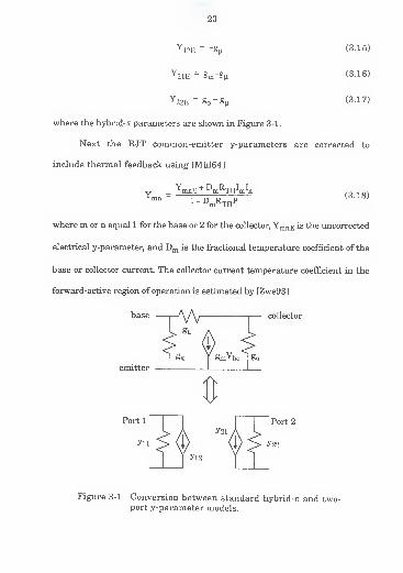
23
Y 12E = Si
Y21E - Sm-g^
(3.15)
(3.16)
(3.17)Y22E = So + gp
where the hybrid-rc parameters are shown in Figure 3-1.
Next the BJT common-emitter y-parameters are corrected to
include thermal feedback using [Miil64]
mn1 " DmRTHP
(3.18)
where m or n equal 1 for the base or 2 for the collector, YmnE is the uncorrected
electrical y-parameter, and Dm is the fractional temperature coefficient of the
base or collector current. The collector current temperature coefficient in the
forward-active region of operation is estimated by [Zwe93]
base -^VV collector
emitter
So
/As
yi2
Figure 3-1 Conversion between standard hybrid-rc and two-port y-parameter models.

24
DC = fl1-1, (3.19)
where
fl
=XTI + qEG/kT - qVBE/kTNp
(3.20)
For the base current temperature coefficient in same region the expression is
DB =BE
f2
vBEqNE ~ kTNE
- XTB + 1bf
VBE<1
(
v
2 kTNF-XTB
i A
/(IBT) (3.21)
where
EGqf2 = XTI+
kT(3.22)
The thermally corrected y-parameters are then converted back to the hybrid-n
form using the following ordered equations:
SH = "Y12
&n = Yll -«n
«m = Y21+«n
(3.23)
(3.24)
(3.25)
g0 = Y22"^ (3-26)
The hybrid-K parameters are then loaded into the admittance matrix. Again,
the advantage here is that no new matrix elements are needed in the Jacobian
to compute the self-heating effects.

25
Flow control
The flowchart of the dc solution routine with self-heating is shown
in Figure 3-2. First, the voltages from the Jacobian matrix solution are
loaded, and the currents are linearly predicted using the conductances,
the change in node voltages from the previous iteration, and the previous
iteration currents. Using these predicted values of current and the node
voltages, the power is computed, followed by the temperature using Rth-
(If the predictive R^h model is used then the value for RrH comes from the
previous iteration.)
Next, the convergence of the currents, voltages, and temperature is
checked. The predicted currents and the node voltages are compared to the
values of the previous iteration, and if each comparison is within its
specified tolerance, the device has converged. If the convergence check
succeeds then the state-variables are saved, the BJT is marked as
converged and the model routine is exited. If the convergence criteria are
not met then the predicted temperature is used to update the parameter
temperature dependences and the currents are computed from the model
equations described in Chapter 2.
With the currents computed from the model, the power, RrH , the
temperature, and the fractional temperature coefficients are computed.
The convergence is checked again for the new current values against the
predicted values computed earlier. If the convergence check succeeds then
the state variables are saved and the BJT is marked as converged. If it

26
Loop begin
Load voltages frommatrix solution
Compute currentpredictions
1
Compute t(
from last
imperatureiteration
r
Check convergenceof predictions against -
last iteration ~l
Recompute temperaturedependences
Compute currentsfrom model
0buu
>doO
Compute temperatureand impedance
Solve linear
equations
z
Load Jacobian
z
Transform back to
hybrid-n
ICorrect for self-heating
A
Transform hybrid-Kto y-parameters
A
Save state variables
i
Check convergence- of currents against
predictions
k
1Save state variables
Done
Figure 3-2 Flowchart of the dc solution for the implicit nodeself-heating approach.

27
fails the state-variables are saved and the matrix load begins. The BJT
conductance values are transformed into y-parameters using (3.14) to
(3.17), corrected for self-heating using (3.18), and converted back to
hybrid-7i form using (3.23) to (3.26). The modified conductances are then
loaded into the Jacobian. After all the BJTs in the circuit have been
processed and loaded into the Jacobian, the linear equation solver is
invoked to generate a new voltage solutions. SPICE continues to iterate
until all the nonlinear devices converge, or a maximum iteration count is
reached.
AC Modifications
For the ac analysis the small-signal power is computed from (3.2).
The hybrid-;: model is transformed into complex y-parameters as follows:
Y 11E = Sn +gn + jw (Cxcb + Cbe
+ Cbc) (3.27)
Y12E = -gn + jw (Cxcb + Cbc ) <328>
Y21E = «m"«n + j(xSm " o>Cbc ) (3.29)
Y22E = So + Sn + j^'Cbc (3 -30)
where Cbe and Cbc are the base-emitter and base-collector capacitances
respectively, xgm is the excess phase term, Cxcb is a base-emitter
transcapacitor controlled by the base-collector voltage, and the other terms are
standard hybrid-rc parameters shown earlier.
The complex form of (3.18) where ZTH is substituted for is used
to modify the y-parameters to include self-heating. The fractional

28
temperature coefficients used are from the dc solution. The thermal
impedance is computed from and C^h given by the user or predicted
from the Rth computed in the dc solution.
The real parts of the y-parameters are transformed back to the real
parts of the hybrid-n model much as in the dc analysis. To transform the
imaginary parts, first (3.30) is solved for C^. Then Cxcb and xgm are solved
from (3.28) and (3.29). Finally, C be is solved from (3.27). After
transforming the modified y-parameters back to the original parameter
set, the Jacobian is loaded and the matrix is solved for the current
frequency.
Advantages and Limitations
This implementation is easy to use; with only a few new model
parameters the user can model self-heating. The changes to the original
SPICE source code are minimal as well, making the model easy to support.
The bias- and frequency-dependent thermal impedance model makes for
smooth, accurate dc and ac simulations.
The self-heating model in this implementation is only valid in the
forward-active region of operation. The most significant self-heating
occurs in the forward-active region, where the collector-base junction has
a large reverse-bias voltage and the high collector current create large
power dissipation. The forward-active region is also the most common
region for analog applications where self-heating has the greatest effect on

29
circuit behavior. It is for these reasons that this implementation has
focused on this region.
The greatest drawback to this implicit temperature approach is the
inability to do transient simulations. SPICE is ill-equipped to solve the
problem for this modeling approach, and this is the ultimate reason why
the explicit thermal node method was implemented.
Explicit Temperature Node Approach
In the previous approach, the temperature was computed implicitly
in each iteration using the voltage and currents of each iterate, and then
modifying the existing internal conductances. In the following approach,
temperature is represented explicitly by the addition of new elements to
the device model, and a thermal subcircuit to model heat flow. A new row
and column was added to the Jacobian along with new state variables for
temperature and power dissipation. The dc, ac and transient analyses can
be all implemented using this thermal node approach. Detailed FORTRAN
code modifications to SPICE2G.6 for this approach can be found in
Appendix B.
The DC Solution
The following is a brief description of the changes made to the
routine that computes the dc solution for the BJT. Starting where the
derivation of (3.6) left off, the new matrix elements are derived. If the
substitutions of collector thermal transconductance, gTC= ICDC , and
temperature,

30
T = RTH P, (3.31)
are made in (3.6) then 1^ becomes
ic = Sovce + Smvbe
+ Vcb + STCT •
(332)
A similar approach used for the base current results in the expression
[b = gnvbe- Vcb + STBT (333)
where gTB = IBDB is the base thermal transconductance. Using the electrical
analogy for (3.31) results in modeling the temperature as a voltage and the
power as a current. To include the power in the Jacobian, it must also be
represented as a linear function of voltages and conductances. Substituting
(3.32) and (3.33) into the expression for power in (3.2) gives the following:
P = (Sovce + gmvbe + Vcb + STCT )VCE < 3 -34 >
+(«n
vbe "Vcb + STBT)VBE + ^ce + Vbe
Using the above equations (3.31) through (3.34) the intrinsic BJT
element stamp is formed:
8m + So + Sn -gH "Sin "So STC
"gn s^ + gn -gn gTB
- gm - gc -sn (gm + gG + g„) (- gTC - gTB )
-1
vb
iC+ i
b
T P
(3.35)
gpb -gpc - gpb RTH +gpt
where gpc = vce(gm + gQ + g^) is the collector power term, gpb
= vbe(gn
-gjl
) is
the base power term, and gpt = vbegTB + v
cegTC is the temperature power
term.

31
The device temperature change is computed at the new device node
by a controlled current source equivalent to the device power dissipation
in series with the effective thermal impedance as shown in Figure 3-3. The
ambient or global temperature of the circuit is represented by ground, and
the TA node in the figure is grounded for most cases.
The power dissipated in the transistor flows through the thermal
impedance producing the effective temperature change of the device. The
base and collector currents are then modified by the new thermal
transconductance elements and the temperature. The thermal resistance
is the sum of the resistances in the thermal impedance network, shown
A/YR,
'gTB AT Srn Vbe So
e
Cthi
IE
CTH2
Figure 3-3 BJT internal large-signal circuit model showingnew temperature node and thermal impedanceladder network.

32
here divided into three poles. Normally the thermal impedance network is
connected to ground at the point TA , but it can be coupled to other devices
through an additional network representing the impedance between BJTs.
Implementation Options
Two choices affected the selection of an implementation strategy.
The first choice was how to implement the thermal impedance subcircuit.
The second choice was how to compute the temperature derivatives.
One way to implement the thermal subcircuit is similar to the
implicit node approach above and would entail coding the subcircuit inside
of SPICE. This requires the BJT matrix size to increase by a row and
column for each new node in the impedance network. For maximum
accuracy this could require as many as five new nodes, which would almost
double the size of the BJT matrix. The topology of the impedance network
would also have to be chosen in advance. The form of the ladder network
shown in Figure 3-3 or the distributed form shown in Figure 3-4 could be
used. Once implemented in the code, whichever topology is chosen cannot
be changed by the user. The advantages of the internal approach are its
Rthi RTH2
MrTH1 'TH2 yTH3
TA
Figure 3-4 Distributed form of the thermal impedancesubcircuit.

33
transparency to the user and the ability to use the bias-dependent dc and
ac impedance model implemented in the implicit node approach.
The other way to implement the thermal subcircuit is to leave it to
the user to specify the thermal impedance network in the circuit
description file just like any other circuit elements. With this approach the
flexibility to use any topography is retained. Computing the thermal
impedance is a task well suited for pre-processing using the SPICE input
processing routines. The biggest advantage to this approach is that
relatively few changes are needed to the BJT matrix and SPICE data
structures, making the implementation much simpler.
The temperature derivatives can be computed analytically or
numerically. When this work began the main interest was in self-heating
effects on dc and ac simulations in the forward-active region where the
effects are greatest. An analytical solution of the temperature derivatives
was practical when considering only the forward-active region, and made
for an elegant implementation in the implicit node approach. However, a
problem arose when a device passed through operating regions where the
derivatives were incorrect. The simple problem of implementing a single
region became complex when analytical expressions for other regions had
to be implemented. A numerical approach to computing the temperature
derivatives improves the problem of regional boundaries. The numerical
derivatives are computed using

34
— *—- (3.36)dT T-T
where x is any temperature dependent variable at the temperature T and x' is
the value of that variable at temperature T a small increment above T. To
implement the numerical derivatives requires each variable, in this case the
collector and base currents, to be computed twice, once at each temperature.
This takes about the same amount of computation as the direct analytical
approach because of the complexity ofthe analytical expressions (see equations
(3.19M3.21)) compared to those of the currents.
SPICE Code Modification
This section details the implementation. While many different
approaches have been tried over the course of this work, only the final
version is covered here. In this implementation the best trade-offs for
efficiency, flexibility, and convergence have been made. The thermal
impedance is described externally in the SPICE input file, and the
derivatives of the collector and base currents with respect to temperature
are computed numerically.
Since the thermal impedance implemented externally to the BJT
model, there are no new model parameters. Only one new device matrix
node has been added for the temperature and four new state variables:
temperature, power dissipation, and the derivatives of the collector and
base currents with respect to temperature. The modifications to the
SPICE data structure are relatively small, but are complicated to realize

35
because of the complexity of the SPICE data structure. Fifteen
subroutines were modified and one new routine added to incorporate the
changes needed for self-heating, but not all of these are discussed here for
the sake of brevity. For more details, see Appendix B.
The format of the BJT device input line was changed to include the
external thermal node. The new BJT line is as follows:
Qxxxx nc nb ne [ns [nt]] model [area] [initial conditions]
where the items in brackets are optional. The substrate node number (ns) and
the temperature node number (nt) are both optional. The substrate node must
always be given if the temperature node is used or differentiating between
them when only one is specified would be impossible. An example circuit
description with self-heating is shown in Figure 3-5 where the substrate node
has been grounded. If the thermal node is not specified the node is assumed
grounded and the standard isothermal model is used.
Once the preprocessing routines were modified to recognize the
thermal node, build the new device matrix row and column, and add the
new state variables, the work of modifying the device model routine for dc
and transient analyses could begin. Note that the temperature state
VCE 1 0 DC 5
VBE 2 0 DC 0.8
Ql 1 2 0 0 3 NPNMODEL
RTH 3 0 500
Figure 3-5 Sample modified BJT circuit description forSPICE with a thermal resistance of 500 K/W.

36
variable stores the change in temperature above the circuit ambient, and
is converted to the absolute temperature only where needed in the model.
Unless otherwise stated, the temperature referred to in the following is
the temperature change.
In the device initialization phase, the temperature is set to zero. No
power has been computed so no temperature change can exist. Next in the
linear extrapolation section the equation for predicting the power is added
and temperature is added to the current prediction equations:
P = P + |ICAVCE |
+ |IBAVBE|(3.37)
where P is the predicted power and P is the power from the previous iteration,
lC = IC + (gm + 8o)AVBE-(So + gm)AVBC + gTCAT ' <3 -38>
and
lB = lB + SnAVBE -§nAVBC + STBAT (3.39)
Next the initial convergence check is changed to include the
temperature. The absolute tolerance on the temperature multiplies the
conversion factor of 100 K/V and the tolerance of the junction voltages.
With only a unity conversion factor, using the default voltage tolerances
would require the temperature to be accurate to 50 uK for convergence.
This is more precision than is needed and discourages convergence.
Scaling the tolerance to 5 mK provides enough accuracy and improves the
robustness of convergence. The power does not need to be included in the

37
check, because it is a linear function of currents and voltages and will
converge when they do.
Similar to the implicit node approach, the temperature update
equations were moved inside the model routine. The model parameters are
adjusted for local changes in temperature in each iteration. After the
initial convergence check and any junction voltage step-size limiting, the
temperature dependences are inserted. A loop is formed around the
temperature-update equations, so they can be used in computing the
numerical derivatives of the currents with respect to temperature. (See
the flowchart in Figure 3-6.) The temperature in augmented by 0.1 K, the
model parameters are adjusted for temperature, and the currents are
computed from the model equations. At this point the high-temperature
current values are temporarily stored and the 0.1 K is subtracted back
from the temperature to return to the original value. The loop returns to
the temperature update and then recomputes the currents for the proper
temperature. The loop is exited and the current derivatives, gTC and gTB ,
are computed using the approximation of (3.36). The choice of 0.1 K for the
temperature change was arrived at empirically; it results in enough
change in the currents so the numerical problem of subtracting two close
numbers of finite precision does not occur, and it is small enough to
preserve accuracy in the approximation.
The power dissipation must be computed before any changes from
reactive currents in the transient analysis can change the base and

38
Loop begin
Load voltages frommatrix solution
Compute currentpredictions
Compute powerprediction
1Check convergence
of predictions againstlast iteration
Save state variables Done
Start derivativeloop
Add delta
temperature
Correct parametersfor temperature
Subtract deltatemperature
Computederivatives
1
Compute currentsfrom model One
time
* Save currents
Check convergenceof currents against
predictions
Save state variables Load Jacobian Solve linearequations
Figure 3-6 Flow chart of BJT model routine.

39
collector current value. The changes in current from reactive elements in
the transient analysis are not real and do not contribute to real power
dissipation. Such charging currents must be dissipated in the device
parasitic resistances to generate temperature changes. Since the reactive
elements of the thermal impedance are denned externally, no changes are
needed to the transient analysis section of the routine.
SPICE includes a second convergence check after the transient
section to compare the currents newly computed from the model to the
predicted currents. As noted previously, it is not necessary to check the
power; the temperature will not change within the model routine. The
state variables are saved and the Jacobian loaded as shown in (3.34) and
(3.35).
The changes to the ac analysis routine are minimal. In addition to
the normal matrix load, the temperature row and column are loaded with
the small-signal equivalent of the dc matrix load.
Advantages and Limitations
Many of the advantages and limitations to the external thermal
impedance approach have already been mentioned, but is worth restating
them. The advantages are many. Since the thermal impedance is
implemented outside the BJT model, any topology or number of time
constants can be used for the thermal equivalent circuit. No new model
parameters and only a few new state variables are required; an internal
thermal impedance would have many of each. The temperature

40
derivatives are computed numerically, improving continuity across
operating region boundaries with little or no additional computational
overhead. Transient analysis is possible where it was not in the implicit
node approach. The biggest limitation is that the thermal impedance is
fixed. Neither bias nor temperature dependences are implemented, and
the smooth frequency-domain solution of (2.20) is unworkable in the
small-signal analysis. Versions of SPICE allowing nonlinear equations in
user-defined controlled sources would make it possible to overcome this
limitation.
Convergence
Self-heating makes convergence harder to reach. The most common
problem with convergence is thermal runaway. SPICE sets the junction
voltages to large values on the first iteration to ensure the devices are on.
With the large forward biases the model equations compute large currents.
After the first matrix solution, the returned node voltages tend to be quite
large. These factors combine to over-predict the power dissipated in the
device, causing an over-prediction of the temperature. The over-predicted
temperature in the second iteration can cause the temperature-dependent
parameters to become large and cause the computed currents to increase
enough to cause the temperature to increase even more. The temperature
and current will grow geometrically until a numerical overflow occurs,
usually after only a few iterations.

41
Sometimes a variation of this thermal runaway occurs where the
simulated temperature becomes high in an iteration and the model
overcompensates causing a negative temperature change, then positive
again, oscillating with increasing magnitude with similar results as
before.
Two controls have been put in place to minimize these problems: a
hard limit that ensures that only positive temperature changes and a
method in which the initial temperature-iteration is skipped. Theses
enhancements were made to both implementations to improve the
likelihood of convergence by preventing the thermal runaway condition.
For the iteration-skipping method, the thermal resistance is always
held to zero on the first iteration. This is done by checking the
initialization flag and skipping the power computations when the flag is
set. The zero power from the first iteration results in zero temperature
change for the second iteration. The BJT currents and voltages usually
settle into the solution region by this time, and the inclusion of self-
heating is a much smaller perturbation on the solution. The resulting
temperature computed from the power at this point will be closer to the
actual value for the BJT, and subsequent iterations usually converge. The
BJT model effectively executes two isothermal iterations before the self-
heating is turned on.
To stop the oscillation a hard temperature limit was added at zero
degrees local temperature change that prevents negative temperature

42
changes. If the model computes a negative temperature change at the
beginning of any iteration the temperature change is set to zero for the
remainder of that iteration. This allows the model to recover from the
oscillation before it becomes a problem, and it prevents endothermic
solutions not supported by the Gummel-Poon model.
A third method could be used to constrain runaway conditions in
nonlinear equation solutions: step-size limiting. This method limits the
amount a solution element (for example: V35;) can change in a single
iteration. This method can work for temperature in the self-heating model,
but the best value to use for the maximum step size is difficult to
determine and varies greatly from device to device and circuit to circuit. A
step size that is too small can slow down convergence noticeably and one
that is too large may only slow down runaway but not prevent it. For the
BJT model this approach for convergence control gives little return for the
computational investment compared to the other two implemented
methods, so it is not used in this implementation. It could be useful,
however, for special cases, especially if the user had control of the
temperature step-size for each transistor.
Results of convergence comparisons between the original isothermal
model and the explicit thermal node approach are shown in the next
chapter. Such comparisons provide only general estimates of the costs of
using self-heating, since convergence in SPICE has seemingly random
behavior for large circuits. For example, modifications to the input such as

43
changing the order in which the elements are listed can affect
convergence.

CHAPTER 4SELF-HEATING IN CIRCUITS
Self-Heating Effects
An easy way to understand self-heating effects in circuits is through
the effects on BJT small-signal parameters [Miil64, Mill70]. Assume that
with self-heating neglected the common-emitter g-parameters are given
by
8llB=l/^E (4.1) g 12E = 0 (4.2)
S21E = 8mE (4 - 3 ) &22E = 1/roE (4.4)
Using the partial derivatives in Chapter 3, when self-heating is considered, the
small-signal collector current becomes
• _ g21Evbe + g22Evce + gcgraMjg vbe + Icvce>
(4 g)1 - DCRTHP
assuming that ic/i
bs IC/IB . Similarly, the base current is
j . gllEvbe + gl2Evce + ^B^TH^B^B vbe + ^cc) /AC ,b I^bW (4 - 6)
Thus the g-parameters, corrected for self-heating, can be expressed as
&HE + PbRth 1!(a j\ 8i2B^Pb^thVc
g11 1-DBRTHPgl2 1-DBRTHP (4.8)
44

45
«21=
(4.9)S22 = §22E + Pc^H 1^
1 - DCRTHP(4.10)
The denominators in (4.7) - (4.10) become significant as the power
approaches the critical values Pc = 1/DCRTH or PB = 1/DBRTH where
plots of Ic and I3 versus the port voltages have infinite slopes. These limits
are related to the onset of second breakdown. In most analog circuits the
power dissipation is kept much less than or PB , so that the effects of
the denominator are negligible except in circuits requiring great precision.
Note that as values for RpH rise, the power required to cause errors
decreases.
Now consider g21 . The electrical-only transconductance g2\E *s
approximately gmE = IC/VT . If the denominator in (4.9) is close to unity,
then the value of g2i, corrected for self-heating, is approximately
821^! + dbrthiBVt)- Similarly, the electrical-only input conductance is
She = 1/rnE = Ib /vt» so that 811 = 1/r*= She* 1 + Dbrth ibvt)- For any
reasonable conditions, the term DBRTHIBVT is very small, so these two
parameters are only affected by the corrections in the denominators,
which require substantial power dissipation approaching PB .
The situation is different for the other two g-parameters. A simple
model for the electrical output conductance is g22E = l/roE= IC/VA ,
where VA is the Early voltage. From (4.10), for P «
P
c ,
S22 = «22e( 1 +dcrth icva)> where the second term in the parentheses can
be thought of as a figure of merit giving the fractional error in the output

46
conductance caused by self-heating for low power. This term can be
substantial even for very modest currents.
Neglecting self-heating, the effects of changes in VCE on IB , and thus
Sl2E» are verv small in forward-active operation; typically g12g can be
neglected in circuit analysis. However, including self-heating and
assuming the denominator in (4.8) to be near unity, this parameter is
much larger in magnitude and positive:
812 = DbRthVc = «22EDBRTHICVA/ P<> (4.11)
This effect is exploited in the next chapter to extract the thermal impedance of
the BJT.
Simulation Examples
The repercussions of the above results for circuit designers are
evident in a variety of circuit types. The following examines the effects of
self-heating on some common circuits. The SPICE circuit descriptions for
all the circuits shown are provided in Appendix D. All the simulations
used the explicit thermal node simulator with thermal impedance
subcircuits.
The most common analog circuit is the common-emitter amplifier
configuration where the emitter and base impedances are typically small
and output (collector) load is large, comparable to r0. Here self-heating can
significantly raise the input resistance and decrease the output resistance.
The result is a greatly reduced gain at low to moderate frequencies where
self-heating predominates. This effect is illustrated in Figure 4-1

47
[Fox93b]. This common-emitter amplifier circuit was originally published
by Lee using the implicit temperature simulator developed in this work
[Lee92]. The rest of the circuits are new examples of self-heating effects
on circuits.
The larger 741 op-amp circuit shown in Figure 4-2 is a common two-
stage amplifier circuit with a low current, low gain differential input stage
and a high current, high gain stage [Gra84]. The dc transfer
7K I>—i i i inn 1—i i i miii 1—i i 1 1
1
iii 1—i i i ii iii i iii i nn 1 iii m il
i
1 1—I'll i i i i m i 1 iii i mi i1 '
102103 104 105 106 107 108
Frequency (Hz)
Figure 4-1 Simulated voltage gain vs. frequency forcommon-emitter amplifier with and without self-
heating. Note that the dc gain is halved by self-heating.

48
characteristics of a 741 op-amp circuit are shown in Figure 4-3 both with
and without self-heating. The self-heating curve shows a significant
nonlinear distortion. This distortion causes a 10% shift in offset voltage
and a large reduction in gain. The greater distortion at low output voltage
Figure 4-2 Schematic for the 741 operational amplifiercircuit. Resistance values are as given by Greyand Meyer [Gra84]

49
indicates the PNP current-mirror in the second amplifying stage, which
has no emitter degeneration, has a much reduced output resistance due to
self-heating.
For the 741 op-amp, the first stage is operated at such a low current
that self-heating effects are minimal. The second stage is operated at
higher currents, and is driven from the low output impedance of an
emitter follower, so there is an error in the dc gain due to self-heating. This
is shown in Figure 4-4. When Miller compensation is applied around the
-15 1 1 ' 1 1 1 » 1 l
0 1 2
Input Voltage (mV)
Figure 4-3 Simulation of dc transfer characteristics of a 741op-amp with and without self-heating.

50
second stage, the dominant pole frequency is also shifted by self-heating.
However, the negative feedback through the compensation capacitor
swamps out the positive thermal feedback above the dominant pole
frequency, so there is little thermal effect on the phase margin.
Some large-signal circuits where precise Vgg matching is important
can be affected by self-heating when the collector-emitter voltages of the
matched BJTs differ. The BJT with the higher Vqe has greater power
100
Frequency (Hz)
Figure 4-4 Simulation of a 741 op-amp open-loop voltagegain with and without self-heating showing theeffects of compensation.

51
dissipation, causing its VgE to decrease to suppress the increase in
collector current. These dc effects were demonstrated for current mirrors
by Munro and Ye [Mun91], and for current reference circuits by Fox and
Lee [Fox93b]. When these circuits are used in switching applications the
VBE shifts settle over long time periods as the BJTs heat and cool.
Consider the pin-driver circuit shown in Figure 4-5. The function of
this circuit is to transfer a voltage level at low-current, high impedance
circuit to a high-current, low-impedance circuit (or package pin). Going
from VIN to Vqut the signal increases two diode drops through Q 1 and Q2
Q3
VOUT
Figure 4-5 Simplified pin-driver circuit.

52
then decreases two diode drops through Q4 and Q2 . If all of the transistors
are matched the output follows the input.
Transistors Q3 and Q2 are diode-connected and do not dissipate
much power. Q± and Q4 can have large collector-base voltages and can
dissipate significant power. Figure 4-6 shows the temperature transients
of Qi and Q4 . For this simulation, the supply voltages Vcc and Vee were
10 V and -10 V, the current sources Ixand I2 were 1 mA and 10 mA, and
50 I—
—
1—
1—'—i—'—i—i—i—i—i—i—i—i—|—I—i—i—I—|—i—i—I—
r
Time ((is)
Figure 4-6 Simulated temperature transients ofQ: and Q4 of
the pin-driver circuit for and 18 V input pulse.
53
the input voltage pulse switched from 2 V to 18 V. The temperature swing
of Q4 is much larger than that of
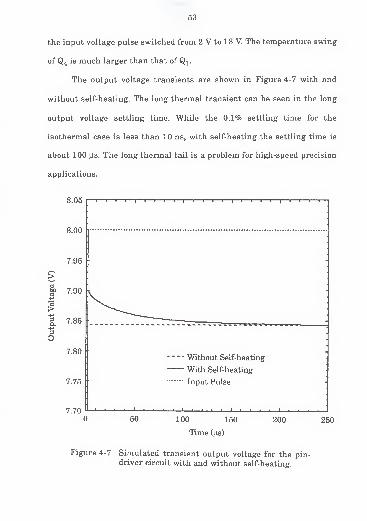
The output voltage transients are shown in Figure 4-7 with and
without self-heating. The long thermal transient can be seen in the long
output voltage settling time. While the 0.1% settling time for the
isothermal case is less than 10 ns, with self-heating the settling time is
about 100 \is. The long thermal tail is a problem for high-speed precision
applications.
8.05
8.00
7.95
7.80
7.75
7.70
T 1
Without Self-heating
With Self-heating
Input Pulse
i J 1 1 i i L _i L
0 50 100 150
Time (|is)
200 250
Figure 4-7 Simulated transient output voltage for the pin-driver circuit with and without self-heating.

54
Another application of self-heating in circuit design is thermal
coupling of transistors that are near each other. The distance for a device
to be considered near to another in thermal terms depends on the circuit.
Fukahori and Grey showed that for a operational amplifier the input
transistors could be affected by the heat generated in high-current output
transistors if they are located close to the input transistors [Fuk76]. They
showed that careful layout that located the output stage away from the
input stage could cure this problem. The general rule in these cases is to
lay out high-power elements of the circuit away from the sensitive
subcircuits of a design.
For the case of multiple-emitter BJTs the above rule does not apply.
These devices are used in high-frequency applications primarily because
of the reduced parasitics from the shorter intrinsic base region and
reduced current crowding of the thinner emitter fingers. To simulate a
multi-emitter BJT with self-heating, it can be separated into multiple
devices, one for each finger. This method was developed in collaboration
with Brodsky [Bro97b]. A schematic for a three-finger BJT is shown in
Figure 4-8. The fingers are thermally coupled by current-controlled
voltage sources (H-sources in SPICE). Each finger's thermal subcircuit
includes an H-source for each of the other fingers. An H-source is
controlled by the power flowing in another thermal subcircuit multiplied
by the thermal resistance between the two fingers.

55
Figure 4-9 shows the result of a dc simulation of the three-finger
BJT. The middle finger is heated more than its neighbors because of its
close proximity to both of the side fingers. It carries more of the base
current and contributes more to the total collector current. The result is a
reduced output impedance over the non-thermal simulation of about 70%
for this example.
Figure 4-8 Schematic for simulating a three-finger-emitterBJT, and the three coupled thermal subcircuits.

56
The simulation of circuits with self-heating adds to the accuracy of
many designs, but is not necessary for all circuits. To further increase the
reliability of simulation results, more accurate model parameters are
needed, including thermal impedance parameters. A technique for
extracting the thermal impedance for BJTs is introduced in the next
chapter. The effects of self-heating on the Gummel-Poon parameter
extraction are also examined.
15.0 I1
1 1 1 1 1 1 1 1
0.0 1 1 1 1 1 — 1 i i •
0.0 2.0 4.0 6.0 8.0 10.0
Collector-Emitter Voltage (V)
Figure 4-9 Contribution of the middle and side fingers to thetotal collector current of a three-finger emitterBJT

67
Convergence Comparison
The simulation statistics for each of the above circuits were
collected for the self-heating and isothermal cases. The results of a three
run average are shown in Table 4-1. The statistics for the multi-finger
Table 4-1 Circuit simulation statistics.
Circuit
Operating-point
Normal/Self-heating
number/time (s)
AcNormal/Self-heating
number/time (s)
Transient
Normal/Self-heating
number/time (s)
Common-emitter NPN
5/0.03 6/0.03 46/0.07 46/0.12
741 Op-amp 15/0.45 15/0.95 46/1.08 46/1.92
Pin-driver 8/0.07 9/0.12 710/2.70 856/5.85
transistor are omitted, because there is not an isothermal equivalent
circuit for comparison. These statistics are reported by the ACCT option
in SPICE the reports on execution times and iterations for each analysis.
The circuits were simulated on a Sun Microsystems, SPARCstation 10
with 64 MB of memory. The computer, at the time of simulation, was only
running the FVWM window manager and common UNIX daemons, so the
simulation time for each circuit was relatively unaffected by resource
demands by other processes. The quality of the computer isolation was
shown to be effective, since each of the averaged simulations returned the
same result.
It is clear that simulations using self-heating have a greater cost in
computation time. For the case of the single-BJT common-emitter circuit
difference in the operating-point solution times is lost in the accuracy of

58
the measurement, but the self-heating circuit needed an extra iteration
implying the need for greater computation time. The ac analysis used 71
percent more time because of the added elements of the thermal
impedance subcircuit. Because of the linear nature of the ac analysis, the
number of iterations is always exactly the same as the number frequency
points computed.
For the 741 op-amp, the iteration count for the operating-point
solution is surprisingly the same, but there is a 111 percent increase in
computation time for self-heating. It is important not to infer too much
from these results, because the bias used for each case was different due
to the shift in operating-point caused by self-heating. A small bias change
for this class of circuits will almost always have an effect on convergence
independent of self-heating. The additional time is due to not only the
added circuit elements but the increase computation need in the BJT
model for self-heating. The ac solution took 78 percent longer, which is
consistent with the common-emitter circuit results.
The pin-driver circuit's initial operating-point solution required one
more iteration and 71 percent greater time per iteration for self-heating.
The effects of self-heating on transient iterations and computation time
are expressed in the time-step control. The SPICE algorithm to compute
the time-step in the transient analysis increases the size of the time step
each iteration until convergence is not reached and then "backs up" to try
a smaller time-step. For the isothermal simulation, there are practically

59
no changes in the output for the majority of the analysis time. SPICE can
take large time-steps and complete the simulation with fewer iterations.
For the self-heating case the long thermal tail requires smaller time-steps
and a greater number of iterations. The time per iteration increased 80
percent.
To keep the added overhead of self-heating to a minimum, it is
important to use the insight provided in the first part of this chapter to
choose the devices most affected for simulating with self-heating. This
mixed approach also can improve convergence behavior over using self-
heating for every BJT in the circuit.
This chapter has used models for thermal impedance for simulation.
In the next chapter, the technique used for extraction of the thermal
impedance is presented. It was shown here that self-heating changes
device performance. The next chapter shows how self-heating can affect
the extraction of the Gummel-Poon model parameters.

CHAPTER 5MEASUREMENT OF MODEL PARAMETERS
This chapter describes methods for extracting model parameters for
use in self-heating circuit simulation. First, a two-part, dc and ac method
for extracting the thermal spreading impedance is shown. The results can
be used to either verify an impedance model or to directly extract the
impedance network for each device [Zwe95a, Zwe96]. Second, the effects
of self-heating on Gummel-Poon dc model parameter extraction are
examined. Self-heating causes errors in certain high-current parameters
if they are extracted under nominally isothermal conditions unless self-
heating is accounted for in the optimization phase [Dav88].
Measurement of the Thermal Impedance
Two components must be characterized for an accurate model: the
thermal spreading impedance (temperature response to a change in
dissipated power), and the temperature dependence of the current-voltage
relationships of the transistor. At first glance measuring the temperature
dependence of the currents appears straightforward; the ambient
temperature is varied by a known amount and the resulting changes in the
terminal currents are measured. Actually the situation is more
complicated because the actual device temperature rises above the
ambient by an unknown amount as a result of self-heating. This unknown
60

61
temperature change can be significant compared to the ambient
temperature change, especially in high-current regions. This chapter
describes a way to overcome this problem, and a way to use the results to
extract the thermal impedance from transient response.
Measurement of the base current response is treated as the
thermometer in the techniques described here. An underlying assumption
of these measurements is that collector-base conductance from the
modulation of the base recombination current is negligible compared to
the effect of self-heating on the total base current. If operation is in the
forward-active region where significant impact-ionization can be avoided,
any change in base current resulting from a change in collector-base
voltage with constant base-emitter voltage is dominated by self-heating.
Characterization of the thermal impedance requires two steps. The first
step involves finding the fractional temperature coefficients: the fractional
change in base or collector current for a unit change in the transistor
temperature with fixed base-emitter voltage. We find this information by
sweeping the dc collector voltage of the transistor at different ambient
temperatures and then cancelling the self-heating. The second step is to
find the thermal impedance from the base current response to a collector
voltage step. Using the temperature coefficient results from the first part,
the base-current response is converted to a temperature response. After
normalizing the transient temperature response by the dissipated power,
the thermal impedance model can be fitted to the waveform.

62
Temperature Coefficient Measurement
In this part of the measurement cycle the goal is to calibrate the
base-current thermometer by measuring the change in current caused by
a change in temperature with fixed base voltage. When the temperature is
increased the collector current and the power increase, causing the local
temperature to increase considerably because of self-heating. An error
arises whenever self-heating contributes significantly to the device
temperature (at moderate to high current levels). Transient
measurements, to be discussed in the next section, are typically made in
these regions, and there needs to be a way to characterize the base current
dependence on temperature in the presence of self-heating. The total
temperature change of a BJT, including self-heating, is given as
AT = RTHAP + ATA = RTH(ICAVC + AICVC ) + ATA (5.1)
where AT is the total temperature change at the emitter, ATA is the ambient
temperature change, and Rrpn is the thermal resistance. Separately measuring
the change in base current caused by a change in ambient temperature and
then by a change in power gives two equations that allow cancellation of the
self-heating from the temperature coefficients. The power is controlled by
varying the collector voltage in the forward-active region where base-collector
conductance is negligible and avoiding regions where impact ionization is
significant.
When changing the ambient temperature with the collector voltage,
Vc ,constant, (5.1) gives a net temperature change of

63
atIavc
= osATa + rthvcaic (5.2)
where
AIC= ^AT = DC ICAT (5.3)
is the change in collector current due to a change in temperature. Substituting
into (5.2) and solving for AT gives
ATAAT
Iavc= o = TT5^v-
c-
(5 - 4)
When is held constant and Vq is varied, (5.1) reduces to
atIat, = o
= RjhC^c + AIcvc) (5.5)
where
AIc=af
AT +aV~
AVc = DcIcAT+ v^c <5 - 6 >
C A
and VA is the Early voltage. Substituting into (5.5) and solving for AT gives
ICRTH AVCATk = 0= 1-DCRTH I
A
CVC •
(5 ' 7)
Notice that the denominators of(5.4) and (5.7) are the same. Combining (3), (5)
and the base-current dependence given by
aiB aiBAIB = ar
AT +av^
AVC :sDB IB(ATA + RTHVCAIc) (5.8)
where the second term is the base-collector conductance (assumed to be
negligible), results in the following ratio:

64
(AIB/AVC )
ATA = 0
(AIfi/ATA )
= ICRTH (1 + VC/VA ). (5.9)
AVc = 0
This can be solved for R^h if VA is known or is much greater than V^. It is
important to note that the thermal resistance found here is an effective value,
and includes the thermal impedance of the package and die. While this is not
an exact value for the intrinsic thermal resistance, it is a good estimate for
extremely low frequencies.
Once Rth is known, (5.8) can be solved for the fractional
temperature coefficient of base current:
Note that this rather complicated procedure is not needed at moderate to low
currents, where self-heating does not need to be cancelled.
The following is a description of the measurement setup and
algorithm. The transistor is connected in common-emitter configuration
inside an oven or on a probe station thermal chuck. It is important to have
stable, accurate ambient temperature control during the measurement,
because the voltage sweep takes a long time and errors in the ambient
temperature significantly affect the accuracy of the results.
The algorithm for the measurement is simple, though very time-
consuming. First, set the ambient temperature and allow it to settle
completely, chose a base voltage for the region of interest (moderate to
ATA + RTHVCAIC(5.10)
AVc = 0

65
high current region), and sweep the collector voltage in the forward-active
region where a noticeable, linear increase in IB can be seen (avoiding any
fall-off due to impact-ionization). Use a very long delay time between
measured points; about 30-60 s typically works well. This allows the self-
heating of the transistor to settle before making the measurement at each
point. Execute the sweep, measuring 1q, Ib> and Vce f°r each Vbe of
interest. Change the temperature and repeat the voltage sweeps done
before (from experience, a temperature step of less than 10 °C is
recommended to avoid errors caused by the strongly nonlinear dependence
of current on temperature). Take the average current changes with respect
to collector voltage and ambient temperature. Using a geometric mean
helps compensate for the non-linearity of the data. Use (5.9) and (5.10)
above to compute the fractional temperature coefficients at each base
voltage value.
Figure 5-1 shows a plot of the temperature coefficients versus base
voltage for an NPN Harris UHF transistor with a 3x50 |im2 emitter. The
UHF process yields high-frequency, dielectrically isolated, vertical
transistors [Dav92]. The collector voltage was swept from 2-4 V while the
base voltage was varied from 700-850 mV in 5 mV intervals using a
Hewlet-Packard 4145A Semiconductor Parameter Analyzer. External
computer control was used to run the HP 4145A, because only short
durations are available for the voltage steps using the integrated
controller. The automation of the experiment also helped reduce human

66
errors and total measurement time by integrating setup, measurement,
and data collection into a single routine. The ambient temperature was
controlled using a Delta Design Model 111 Thermal Chamber;
temperatures used were 25 and 33 °C.
This measurement has errors that are dominated by oven-
temperature accuracy, non-linearity of the data, and effects of base and
emitter resistances. The thermal chamber has a published repeatability
t 1 1 11
1 1 1 11 1 1 1 r
0.70 0.75 0.80 0.85
Base Voltage (V)
Figure 5-1 Harris 3x50^im UHFN3 bipolar transistorfractional temperature coefficients of base andcollector currents versus base-emitter voltagemeasured with and without correcting for self-
heating.

67
accuracy of 0.5 °C and a relative error of 0.1 °C. The absolute error is not
as important for the temperature coefficient measurement as the relative
error since the change in temperature is used in the computations.
Because the measurements shown here were repeatable with an error
consistent with the 0.1 °C, the published errors can be believed. The
emitter and base resistances cause a slight error in the intrinsic VBE for
high currents. When AIC is 1 mA the intrinsic AVBE is reduced by 2 mV.
The total error for the experiment is approximately 1 0 percent.
Thermal Impedance Measurement
The objective of this part of the measurement cycle is to measure the
normalized thermal response to a step in power. This is done by converting
the base current response into a temperature response using the
temperature coefficients extracted above. Solving the fractional
temperature coefficient definition for the change in temperature gives
where Iq is the median value of the base current for the transient. At this point
the signal represents the thermal transient for the power step applied, and it
must be normalized for a unit power step. This is done by dividing the AT(t)
signal by the power of the step:
AT(t) =IB (t) - IB (0)
rBDB(5.11)
AT (0 = AT(t)(5.12)norm AICVC + AVCIC
where the denominator term is the magnitude of the power step.

68
The setup for this measurement is similar to the temperature
coefficient common-emitter configuration with a collector voltage step
applied instead of a slow voltage sweep. The setup is shown in Figure 5-2,
where the BJT in the center is the test device being probed on a wafer. The
current-to-voltage converter transforms the base current into a voltage
waveform for the oscilloscope. With the base voltage held constant, the
base current is
V<) = (Vqut - vbe)/rf (5.13)
where is the feedback resistance. Unfortunately, the intrinsic base-emitter
voltage is not constant because of the parasitic base and emitter resistances.
Since the change is small compared to the thermal voltage, a linear correction
is suitable:
WO =VQUT ~ VBE
RF -RB -(1 + P)RE(5.14)
where Rg and R^ are estimated base and emitter resistances and (3 is the large-
signal current gain.
RS=50Q
Vc Pulse
Generator
^3-RF=51(K>
<u
MlcoaCO
Figure 5-2 Schematic for the transient responsemeasurement.

69
There are important practical trade-offs in choosing the feedback
resistor value. The most important is the gain versus bandwidth trade-off.
Gain must be large because the signals of interest are typically very small,
yet a wide bandwidth of about 100 MHz must maintained to resolve the
earliest part of the transient response. In our measurements, an amplifier
with gain-bandwidth of 1 GHz was used with RF = 510 Q and RscOPE =
50Q for a loop gain of about 1 0 and a bandwidth of 1 00 MHz. The "sponges"
shown in Figure 5-2 are high-frequency sinks that absorb the energy at
frequencies beyond those ofinterest in the thermal measurement; they are
required to keep the UHF transistors from oscillating. The sponges also
help absorb some of reflected power from the unmatched impedances of the
pulse generator and BJT collector. The device under test was probed on-
wafer using one meter, 50 Q. co-axial cables.
The following is a description of the method used to make the step-
response measurement. First, a value of base voltage was selected to give
a current large enough that the collector voltage step created enough
power to get a measurable change in base current for a square wave
collector voltage of 2-5 V. The best frequency to use for the square wave
depends on the transistor; the response must settle before the end of each
half cycle. Much of the response occurs in the first 50 us, but it continues
until about 1 ms, after which package heating dominates. Because of the
distributed nature of the response, the op-amp output was recorded using
three overlapping time windows of increasing size to capture with high

70
resolution the fast beginning of the response while keeping the number of
data points to a minimum for the long tail. Next, the pulse generator was
set to dc output and an ammeter was connected in series with the collector
to measure the collector current at the pulse maximum and minimum
values. The op-amp output is also measured at this time to compute the
base current from (5.14). From this data the (3 of the transistor is
determined, so that the transient base current can be converted into a
collector current for computation of the power step magnitude. The base
current minimum and maximum in this dc measurement differ from the
values in the transient because of the difference in mean power being
dissipated. Using (5.11) and (5.12), the normalized temperature response
can be computed. Figure 5-3 shows the normalized temperature responses
for a range of geometries.
Figure 5-4 shows the thermal resistance of the same transistors
versus emitter width. Estimated errors for the measurement are also
shown. These errors are primarily from three sources: errors in the
extracted fractional temperature coefficient, the variance of (3 over the
range of collector voltage, and the absolute error of the measured base
current.
The absolute error of the base current seriously limits accuracy for
small transistors that operate at low currents where it is difficult to get a
large enough change in IB to be seen over the noise of the measurement
equipment. This does not mean that thermal effects in these transistors

71
are insignificant. In the setup used here the limit for dc collector current
is approximately 1 mA. For a small transistor biased at 1 mA undergoing
a 5 mW power step with an RTH of 500 K/W, an approximately 15%
increase in IB occurs. However, this change is seen as only 1 mV at the op-
amp output. This signal is hard to resolve with a oscilloscope with a 1 mV/
division minimum resolution. Add to that a typical 2 mV of noise
superimposed on this signal, and it becomes very difficult to resolve the
transient even with averaging.
400
350
300
« 250
8 200
BUH8 150
N—E 100coZ
50
01
—i ii
G—03x30—B3x50
3—03x70
A—A3x90<—<3xll0
V—V3xl70|>—£>3x210
i i 1 1 11
1
i i—i i 1 1 1
1
-5010- 10
-610"5
Time [s]
10" 10-3
Figure 5-3 Normalized temperature response versus time ofthe UHF transistor for seven different emitterwidths.

72
Thermal Impedance Model and SPICE
The above results must be compressed into a manageable model for
use in circuit simulation. Using the version of SPICE modified to include
a temperature (AT) terminal described in the previous chapter, the
thermal impedance can be incorporated into precision circuit simulation
of dc, ac and transient. To convert the measured step-response data to an
equivalent RC-ladder model, the program TIPP was used to provide
SPICE with calculated values for the thermal resistance and thermal
capacitance components needed for the thermal equivalent circuit [Bro93].
TIPP can handle up to five poles for the thermal-impedance model, and
input can come from either measured transient data (AT vs. time as found
400
0 1—1—1—1—1—1—•—1—~——'—————i———.—.—i . , . -J0 50 100 150 200 250
Emitter Width [|!m]
Figure 5-4 Thermal resistance versus emitter width for theUHF transistor with emitter length of 3 (im

73
here) or a predictive physical model [Joy70]. Figure 5-5 shows the
normalized temperature response for a 3x70 |im2 transistor and the
resulting three-pole and single-pole fits. The three-pole fit is good, and
generally is the best trade-off between accuracy and complexity for
precision applications. For some situations the single-pole model is
sufficient.
Many issues must be considered when deciding whether to use
measurement or a physics-based predictive model for determining the
thermal impedance in a process. Typically, manufacturers extract model
parameters for each transistor in a process from measurement. The
Time [s]
Figure 5-5 Comparison of normalized temperature responsefor one and two pole fits and measured data of theUHF 3x70 |im transistor

74
extraction is automated and can be done fairly quickly. If the
measurement of the thermal impedance is included in the extraction, the
time spent on each transistor is greatly increased.
Consider just the calibration step of extracting the current
temperature coefficients. Estimating that each data point takes 30 s and
that the minimal of two Vqe values per Vg^ (which could case large errors)
for two temperatures, gives a minimum of 2 minutes per VBE . Add to that
the time for the change of temperature of approximately 10 min and the
time to find the correct operating region for the measurement. This takes
about 30 min per transistor before the transient measurement has been
made.
Considering the time that would be required to measure parameters
for every BJT geometry, development of a model for thermal impedance
dependent on process parameters that scales with transistor geometry
would be preferable. Such a model should use physics as much as possible
but exclusively. The trade-off here is the accuracy. A physical model cannot
include all effects and still yield results quickly. For each neglected effect
the accuracy usually decreases. For some structures the assumptions
needed to solve the heat-flow equations may not allow enough accuracy to
be useful. For these structures the loss of accuracy in the physics can
usually be corrected by using empiricism and the information from
measuring only a few transistors. In the case of a vertical, junction-
isolated, rectangular emitter BJT good predictive physics-based models

75
exist (such as the one described in Chapter 2). For the wafer-bonded UHF
transistors measured here, a scalable thermal model is difficult to develop
due to the large process variation of the oxide depth that greatly affects
the thermal impedance. For thin SOI technologies where the isolation
depth and thickness are well-controlled, physical modeling seems simple
until the increased importance of heat-flow out the contacts and wires is
considered. Extraction of thermal impedance for some transistors in a
process will always be needed either to validate a model or to tune some
empirical parameters. A reasonable goal is to avoid spending needlessly
long times measuring every BJT in a process.
Self-heating and Model Parameter Extraction
When standard parameter-extraction procedures are used to find
parameters such as Early voltage and knee current, the data typically
include some self-heating effects. When these parameters are used in a
model with self-heating, the self-heating effects are overrepresented. For
accurate modeling, the parameter extraction procedures themselves must
be modified to separate thermal and electrical effects. This section
describes a process to accurately extract these high-current parameters.
Most of the SPICE Gummel-Poon model parameters are normally
extracted in low-power regions where self-heating effects can be ignored.
Three parameters, however, are usually extracted in high-power regions
where self-heating can be important. These are the knee current, the
Early voltage, and the parasitic base resistance (RB ). IKF and RB are

76
extracted from a Gummel plot at high current, usually with a significant
base-collector voltage to avoid quasi-saturation, so that power dissipation
may not be negligible. VA is extracted from the slope of a collector current
versus collector-emitter voltage plot, which is very sensitive to the power
dissipation of the measured device. It is tempting to try pulse
measurements to avoid self-heating-induced problems by measuring the
device before it can heat up. Unfortunately, because the thermal response
in scaled devices has time constants on the order of nanoseconds, it is very
difficult to measure a BJT in electrical steady-state before significant self-
heating begins. In the approach presented here, the device is allowed to
reach thermal steady state before data is recorded.
For comparison, a normal isothermal extraction not accounting for
self-heating was done first. The model parameters were extracted and
optimized in the normal way for a packaged 1.6 x 5 (|im)2
,junction
isolated, NPN transistor obtained from Analog Devices [Get78]. All
measurements were made using a temperature-controlled oven to supply
a constant ambient temperature. The data for the characteristic curves
shown in Figure 5-6 were measured from a 0-3 V sweep of the collector-
emitter voltage with the base voltage held constant at 0.8, 0.85, and 0.9 V.
Each point is the average of 16 measurements made after holding the bias
for 20 seconds so the temperature could stabilize. The same delay-and-
measure technique was used to record the Gummel plots used in the
extraction. For the Gummel plots the base-emitter voltage was swept from

77
0.5-1.1 V with the collector-base voltage held constant at 0.5 V to avoid
quasi-saturation. Note that it would not be uncommon to use a V^b of 1 V,
doubling the power dissipation seen here.
After the device Gummel plots and characteristic plots were
measured at several temperatures, the initial parameter set was extracted
using the curve-fitting techniques described by Getreu [Get78]. The
exception to this was the base and emitter resistances were extracted
using the method described by Ning and Tang [Nin84]. This is an adequate
4.0 i» » ' i
ii i < ' i ' i » i
0 0 1 1 ' ' 1 1 1 I I 1 -i_ 1
' 0.0 1.0 2.0 3.0
Collector-Emitter Voltage (V)
Figure 5-6 Characteristic curves resulting from a normalmodel parameter extraction.

78
method for getting values for these parasitic parameters when ac methods
are unavailable. The extraction was for only the parameters needed for
simulation of the forward-active and saturation regions; the reverse
modes of operation were ignored because of their infrequent use in circuit
design and the obvious extension from the forward modes examined here.
Next the model parameters were tuned using nonlinear
optimization, the extracted data, and the output of SPICE simulations of
the measurement using the parameters. Most of the parameters required
only small corrections with the exception of the Early Voltage. Results of
the optimization are shown in Figure 5-6. This simulation result is a poor
fit to the measured data especially at high currents where the effects of
self-heating can be seen in the increased slope of the Iq versus V^e curve.
One way to correct for such self-heating errors is to measure the
thermal resistance and use it with the self heating model in SPICE. The
extracted effective thermal resistance using (5.9) was 800 K/W. To
complete the self-heating model, the SPICE thermal parameters XTI and
XTB were also extracted using the measured data over many
temperatures. The resulting fits to the data are shown in Figure 5-7 and
Figure 5-8. When self-heating is added to the simulation using the same
model parameters, as shown in Figure 5-9, the conductance modeling is
improved but the accuracy of the current modeling is not. It is not enough
to simply include self-heating after an isothermal extraction.

79
The model parameters were optimized once more, this time
including self-heating in the model. The Early voltage was not optimized;
the value computed from (5.9) during the thermal resistance extraction
was used instead. The results are shown in Figure 5-10. The fit to the data
is much improved with good agreement in both slope and magnitude of the
collector current.
The model parameter optimization including self-heating only
affected three parameters significantly: VA , and Rb- The value of Ij^p
10 12 -i—i—i—i | i—i—i—i | i i i—i—|—
r
™i 1 1 V
20
_i i i i_
O Measured Data— Model
J L.
30 40 50 60
Temperature (°C)
70 80
Figure 5-7 Resulting model fit for extraction of XTI from theIg versus temperature data.

80
in this optimization was 40% lower than that found in the isothermal
extraction. Self-heating increases the collector current in the isothermal
extraction, so the electrical value of knee-current is overestimated. A 50%
increase in the electrical value VA results from taking into account the
increased slope of the characteristic curves due to self-heating. Finally, a
25% decrease in the base resistance is likely caused by temperature
dependence of the current gain. Although the change in base resistance
1 80i
—
'——i i
i—i—i—i—i—i—i—i—i—i—i—i—i—i—i—i—i—i—i—i—i—i—i—i—i
—
O
14020 30 40 50
Temperature (°C)
j i , L
70 80
Figure 5-8 Resulting model fit for extraction ofXTB from theversus temperature data.
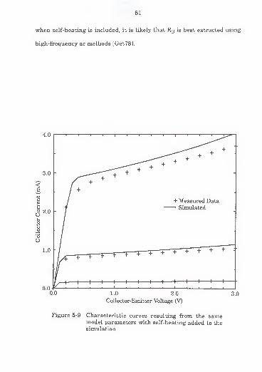
81
when self-heating is included, it is likely that RB is best extracted using
high-frequency ac methods [Get78].
Collector-Emitter Voltage (V)
Figure 5-9 Characteristic curves resulting from the samemodel parameters with self-heating added to thesimulation.

82
Figure 5-10 Characteristic curves resulting from including
self-heating in the extraction process.

CHAPTER 6SELF-HEATING FOR SOISPICE
SOISPICE is a simulation tool developed at the University of
Florida to do physics-based modeling of silicon-on-insulator metal-oxide-
silicon field-effect transistors, SOI MOSFETs, for circuit simulation
[Fos96, Suh95, Yeh95]. The basic structure for these devices is shown in
Figure 6-1. There are two variations of this device, differing in the
thickness of the body layer. In one case the body layer is thick enough so
that in normal saturation region operation the depletion region does not
reach the bottom of the body, and in the other case the body is thin enough
for the depletion region to reach the bottom. These structures are called
either partially depleted, PD, or fully depleted, FD, SOI MOSFETs.
Source Gate Drain
Back Gate / Substrate
I ISilicon Q Silicon Dioxide Q Polysilicon
Figure 6-1 Basic structure of a SOIMOSFET with Si02insulating layer.
83

84
The SOI MOSFET device is surrounded on all sides with an
insulating layer, usually Si02 , that forms a barrier to heat flow. SOI
devices tend to get much hotter than their bulk-silicon counterparts,
because the heat is trapped in the small silicon island the device is built
in [Goo95]. The dominant temperature-dependent effect on MOSFET
current is the carrier mobility, which is a much weaker function of
temperature than the dominant effect (carrier concentration) on BJT
current. For comparable thermal impedances and power dissipations, self-
heating can be ignored in a bulk MOSFET when it cannot in a BJT.
Because of the insulation layer surrounding a SOI MOSFET, the thermal
impedance can be one or two orders of magnitude greater than that of a
comparable geometry bulk device. This increase in thermal impedance
causes generation of much greater temperatures within the SOI MOSFET,
and even the weak temperature dependencies of the transistor become
significant.
Self-Heating Implementation
The following shows how the self-heating model was implemented
into SOISPICE, and then some simple circuit simulation examples are
shown. The implementation has many similarities to the BJT approach,
but some major differences exist. Some of the differences result from the
organization of SOISPICE. Other differences were requested by
SOISPICE users, who preferred a single-pole thermal impedance,
implemented internally, without additional input-file circuit elements, as

85
was done in the BJT implementation. The organization of the SOI
MOSFET model allows all of the current and voltage derivatives to be
easily computed numerically. This numerical approach was a necessity,
because few of the physical model equations have closed-form solutions for
their derivatives. The following discussion will focus on these features
that were unique to the SOISPICE self-heating implementation. The
details of the SOI MOSFET electrical modeling are still under
development and are beyond the scope of this work, so they will be ignored
when possible. Detailed FORTRAN code modifications to SOISPICE for
this self-heating model can be found in Appendix C.
The SOI MOSFET Model
For reference, the schematic for the SOI MOSFET model is shown
in Figure 6-2. The model has many current sources, but most are reactive
and dissipate no real power. The dominant sources of real power are the
channel current, IcH , and the parasitic BJT current, Igj-p The other real
current sources, IRQtand Iqj are orders of magnitude smaller and do not
contribute significantly to the power dissipation. Other sources of power
dissipation include the parasitic resistances, specifically the drain and
source resistances. These may not always be negligible in computing the
total power dissipation, but a problem arises with the thermal impedance
modeling if they are included. The thermal impedance modeling assumes
the power is generated in the channel region under the gate, and not in
the large adjacent source and drain regions. However, since this
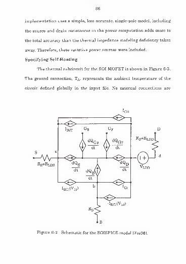
86
implementation uses a simple, less accurate, single-pole model, including
the source and drain resistances in the power computation adds more to
the total accuracy than the thermal impedance modeling deficiency takes
away. Therefore, these resistive power sources were included.
Specifying Self-Heating
The thermal subcircuit for the SOI MOFET is shown in Figure 6-3.
The ground connection, TA,represents the ambient temperature of the
circuit defined globally in the input file. No external connections are
!ch
Figure 6-2 Schematic for the SOISPICE model [Fos96].

87
allowed to the thermal circuit in this implementation so the device
description line becomes:
Zxxxx nd ngf ns ngb [nb] [BJT] model RTH= CTH= L= W= ...
where RTH and CTH are two new device-line parameters that describe the
thermal subcircuit. Ifthe parameter RTH is not specified on the device fine, the
thermal subcircuit is not generated, and the standard isothermal model is
used. Since there are no external connections to the thermal subcircuit and the
ground node is already defined, only one new node is needed to define the
temperature in the self-heating model, so only one new row and column are
added to the device matrix.
Computing the Derivatives
SOISPICE computes all of the current and charge derivatives with
respect to node voltages numerically. The currents are computed from the
model equations once at the bias point of the current iteration. For each
node voltage the model is recomputed with a perturbation, and a finite-
difference approximation to the derivative with respect the node voltage
is computed. For self-heating this process is extended to include another
Source
Figure 6-3 The thermal subcircuit added to theSOIMOSFET model for simulating self-heating.

88
perturbation computation for the temperature, and the power is added to
the list of currents. For this process to have the desired results, the model
equations must include a power computation and the equations for the
model parameter temperature dependence.
Computing the Power Dissipation
The equation used for the power dissipation is
p = I^h + ^jtIVcIs + ^ch + ^jtI^Rd + Rs + Rldd + Rlds)' <6-D
where Iqh is the channel current, Ibjt is the parasitic BJT collector current,
and Rg are the drain and source resistances, and Rldd Rlds are the
low doped drain and source region resistances. The other modeled currents
that are not included in this power dissipation computation, the thermal
generation and impact-ionization currents, flow in regions away from the
channel and are an order ofmagnitude smaller than the two included currents.
Local Temperature Update of Parameters
The second task of including the temperature dependence of the
model parameters is achieved using a new subroutine. This subroutine
contains all of the SOI MOSFET temperature equations found in the
global temperature update routines. These equations have been optimized
to reduce computation time. The parameters affected are shown in Table
6-1 with a short description of each one. These dependencies were
implemented for the SOISPICE global temperature model by Glen Workman
[Wor96]. Equations for both the partially depleted and fully depleted
devices are included in the subroutine. A flag is used to select between

89
Table 6-1 List of model parameters with temperature
dependence.
Pq i*o rn of o»<X ciL CtHlC lei
Name
XNIN Intrinsic carrier density
EGFET Silicon energy gap
VTT Local Thermal Voltage
XMULDSJ LDD carrier mobility
XMUBH Minority carrier mobility in high-doped body
UO Zero field electron mobility
VSAT Carrier saturated drift velocity
WKF Front-gate work function difference
WKB Back-gate work function difference
VFBF Front-gate flat-band voltage
VFBB Back-gate flat-band voltage
JRO Body-source junction recombination current coefficient
ALPHA Impact-ionization parameter a0
TAUG Carrier lifetime in lightly doped region
VBI Source to bulk built-in potential
PHIB Twice Fermi potential ofbody
RLDD LDD sheet resistivity
BETA P
FSAT fsat
equations that the PD and FD devices do not have in common. The result
is that only one routine must be modified if the temperature equations are
modified in the future. As was the case in the BJT self-heating
implementation, the thermal voltage must be treated with special care.
This parameter is defined globally for all devices in SPICE, and a local
90
value (shown as VTT in Table 6-1) must be denned for the model
equations.
Loading the Jacobian
The loading of the self-heating elements into the Jacobian matrix is
done methodically. The current derivatives with respect to temperature
are loaded in the new temperature column at the rows corresponding to
the current branch nodes with the sign indicating direction of flow. The
power derivatives with respect to voltage are loaded in the temperature
row at the columns corresponding to the two nodes that comprise each
voltage. The thermal conductance is loaded at the temperature diagonal
element. The terms associated with the thermal capacitance are not
loaded at this point, but instead are handled during preprocessing. The
Jacobian matrix load for the ac analysis is implemented in nearly the same
way, using complex variables for the reactive elements instead of the
current-conductance pairs of the transient analysis. The simplified
flowchart of how the thermal model implementation works is shown in
Figure 6-4.
SOISPICE already has the capability to deal with linear capacitors.
It is a burden on the programer to implement all of the state variables and
computations to provide for the thermal capacitance inside the SOI
MOSFET routines. By developing a way to trick SOISPICE into believing
that the thermal capacitance is the same as any other capacitance,
SOISPICE processes the thermal capacitance with all of the other circuit

91
linear capacitor elements. This is done by adding a feature to the
SOISPICE FIND subroutine. The last argument of the subroutine call,
IFORCE, is used either to return the location of a device in memory or
create space in memory and store a device there. The latter option checks
whether the device has an unique name and returns an error if it does not.
A third option was added that stores the device without checking the name
uniqueness. Using this option the thermal capacitors are all added to the
READIN
MODCHK
TMPUPD
INFDFET
Decode device line including RTH and CTH
Check if thermal model is needed.1 . If so, generate thermal subcircuit.
1FIND Add CTH to the list
of circuit capacitors.
Update model parameters for ambienttemperature.
Start Newton loop
1NFDID
Compute derivatives for theJacobian including temperature.
1NFDMOD
Evaluate model at localtemperature.
SOITMP
Done
New routine to updatemodel parameters forlocal temperature
Figure 6-4 Flowchart of SIOSPICE execution showingprocessing done for self-heating.
92
bottom of the normal capacitor list with the proper connections to their
thermal subcircuits, all having the same name to avoid possible name
collisions with the regular circuit capacitors. SOISPICE then processes
the thermal capacitors like any other linear capacitor in the circuit
without adding more code to the SOI MOSFET model routines.
This approach also improves efficiency. Since any computations
added to the model routines are executed twice per iteration to compute
the partial derivatives, excluding the computations associated with
thermal capacitance from the model routines reduces computational
overhead.
Convergence Issues
Because of floating-body effects and other complex SOI MOSFET
effects, convergence control and initial conditions must be set with care
even without self-heating to achieve convergence of some circuits. Self-
heating tends to degrade the robustness of convergence, but this is
expected any time the dimension of the Jacobian is increased as it is for
self-heating. The difficulty of estimating the extent of the degradation is
exacerbated by the convergence behavior of the isothermal model, which
was being refined concurrently with the self-heating implementation.
Either the technique of skipping the first Newton iteration as used in the
BJT implementation or a traditional temperature step-size limiting
algorithm could be incorporated to enhance convergence.

93
Simulation Results
Three example circuits were simulated to illustrate some of the
effects of self-heating. The first is a dc simulation to generate the
characteristic curves. The common-source configuration is used with the
source-drain voltage swept from 0 to 3 V for three different gate voltages.
The results for the floating body case are shown in Figure 6-5.
5.0
Drain-Source Voltage (V)
Figure 6-5 DC-sweep simulation for an n-channel, floating-
body, PD, SOI MOSFET with 0.2 urn length and10 um width. VDS was swept from 0 to 3 V for VGof 1, 1.5 and 2 V. The thermal resistance was 5kW/K

94
The second is a step-response test of a single n-channel, PD, SOI
MOSFET. Again, the common-source configuration is used with the gate
biased for the saturation region. The drain voltage is then pulsed. The
resulting drain current response is shown in Figure 6-6. Unlike the BJT
behavior, the current decreases from the effects of self-heating. The
dominant temperature-dependent carrier mobility decreases with
temperature and the drain current along with it. Other than the obvious
4.5 I
>1 >
11
1 11
1
Self-heating
No Self-heating
J
JQ 3.5
3.00.0 0.1 0.2 0.3 0.4
Time ((is)
0.5
Figure 6-6 Transient current response to a drain voltagestep for a common-source, n-channel, 0.2x1 Oum,PD, SOI MOSFET. Vg=2V Vds=2-3V Rth=5kW/K

95
biasing errors that can result, this negative temperature coefficient can
cause hysteresis in the dc transfer characteristic when the thermal
resistance-drain current product reaches a critical value [Fox93a].
The third example demonstrates that self-heating is not a
significant problem for complementary MOS logic circuits; the primary
application for SOI MOSFETs currently. The circuit for a clocked
complementary SOI MOSFET inverter is shown in Figure 6-7. Figure 6-8
shows the output voltage waveform and the temperature waveform of the
n-channel device. Notice that the temperature increases in steps
synchronized with the switching of the inverter. The only time a
complementary gate dissipates significant power is during switching. This
is shown as a steep step in the temperature waveform, and a slow cooling
until the next transition. The simulation shows the temperature
Figure 6-7 Complementary inverter circuit used for dynamicpower dissipation example. ViN is pulsed from 0-
3 V at a frequency of 40 MHz and VDD is 3 V.

96
approaching a steady-state value. The final value of the temperature is a
function of the total dynamic power dissipation for the inverter:
,2
PD =cL(vDD )
(6.2)
where CL is the load capacitance, VDD is the gate bias voltage, and t is the
period of the clocking signal. For the inverter used here,
,2
_ 0.5pF(3V) =25 ns
(6.3)
4.0
> 3.0
sr+^i—
i
2.0
1.0
fo 0.0 u
& 0.6
u8
I
1.0
Time ((is)
Figure 6-8 Inverter output (top) and temperature change(bottom).

97
Since Pq is the total power for the inverter, half of the power is dissipated in
each transistor. Multiplying half the result of (6.3) by the thermal resistance of
5 kK/W gives about 0.5 K increase in temperature, which is consistent with the
simulation steady-state temperature. Such a temperature increase is too small
to significantly affect the circuit performance, which is highly typical of self-
heating in CMOS digital circuits. This is not to say that thermal effects cannot
be important in digital circuits. The heat generated must ultimately leave the
package, and for large, dense circuits the thermal impedance of the die-to-
package-to-ambient is important for reliability, since it controls the rise in
average temperature. However, self-heating is usually insignificant, since the
instantaneous device temperature does not follow the instantaneous power
dissipation.
Conclusion
A self-heating implementation was shown for the SOI MOSFET
models in SOISPICE. A single-pole thermal subcircuit was added to model
the power dissipation through the thermal impedance of the device. Three
example simulations were shown. The step response showed how the
negative temperature coefficient of the current affects biasing and other
analog applications. The inverter simulation demonstrated CMOS logic
circuitry where the contribution of self-heating to the device temperature
is insignificant. The greatest impact of self-heating in SOI MOSFET
circuits will likely be on analog circuits and in parameter extraction.

CHAPTER 7
CONCLUSION
An extensive study of self-heating modeling and effects has been
presented here. A historical look at self-heating for circuit simulation
showed some continuing deficiencies in modeling. The quality of the
modeling has been improved by this work in several areas. Three
implementations of self-heating in the popular circuit simulator SPICE
were shown: two for BJTs and one for PD and FD, SOI MOSFETs. Circuit
effects of self-heating were examined for dc, ac, and transient analysis. A
new measurement technique for extraction of thermal parameters was
presented.
The two approaches to implementing self-heating in the Gummel-
Poon, BJT model each had their advantages. The implicit temperature
approach did not require any changes to the Jacobian matrix. This
approach works well for dc and ac analyses, allowing physically accurate
modeling of the thermal impedance. The inability of this implementation
to simulate transient analyses necessitated finding a different approach
that could. The second approach enabled transient analysis by treating
the power dissipation as an electrical analog. The power and thermal
impedance formed a thermal subcircuit that allowed explicit computation
of a temperature increase. The thermal subcircuit required extending the
98

99
device matrix to include the explicit temperature node. Because the
thermal impedance is modeled with an RC network, a trade-off between
accuracy and complexity was required. The circuit application determines
the level of accuracy needed.
The last implementation for the SOISPICE models PD and FD, SOI
MOSFETs used a single-pole thermal subcircuit model to model self-
heating. The simplicity of the thermal model is reflected in its easy use,
requiring only two new parameters on the device line. A numerical
approach to computing the derivatives for all of the elements of the
Jacobian made the addition the matrix node for temperature easier than
the previous implementations for BJTs.
An examination of the effects of self-heating on circuit performance
was presented that included techniques for analyzing these effects in hand
calculations. Simulations of a common-emitter amplifier showed the ac
and dc effects on open-loop gain and the transfer function distortion for
BJTs. The pin-driver circuit demonstrated how long thermal settling
times can occur in switching applications. The SOI MOSFET simulations
showed that care must be used in analog circuits and that digital
applications are not directly affected by self-heating.
A new measurement technique for extracting the thermal
impedance of BJTs was shown. The two-step procedure used a dc
calibration step to extract the current temperature coefficients, and a
high- speed measurement of the base current step response to extract the

100
temperature waveform. The results of the first step are then used to scale
the base current into temperature. After normalizing for power, the
temperature response is fitted with a multiple-pole model for use in the
thermal subcircuit.
The effects of self-heating on Gummel-Poon model parameter
extraction was examined by including the self-heating model in the
optimization simulation. The Early voltage, knee current, and base
resistance were shown to be the parameters affected most by self-heating.
Self-heating is a potentially important effect that all circuit
designers should be conscious of in their designs. It can have devastating
effects on some precision circuits if not accounted for before
manufacturing. Self-heating is not an important factor in every circuit, so
designers should use discretion when using it in simulation. There are
penalties in simulation time and convergence if self-heating is applied
carelessly.

APPENDIX ASPICE 2G.6 CODE CHANGES FOR MODELING OF SELF-HEATING
USING THE IMPICIT TEMPERATURE APPROACH
The following is a summary of the changes made to SPICE 2G.6 to
implement self-heating in the BJT model. The local temperature of each
device is computed for each iteration as a function of the power dissipation
in the collector-base space-charge region (SCR). Temperature is not
treated as a state variable, and does not require addition of a new row and
column in the circuit matrix for each BJT.
Data structure expansion for new model parameters
The SPICE data structure must be expanded to include the new
model parameters, state variables, and device variables necessary for the
thermal model. A subset of the following six new model parameters are
needed to specify the thermal model shown in Table A-l.
Table A-l Added model paramters.
RTH Thermal resistance
CTH Thermal capacitance
NEPI Epi-layer doping concentration
LTH Emitter length
WTH Emitter width
DTH Collector-base junction depth
101

102
RTH and CTH combine for the single-pole model for the thermal impedance,
ZTH, or ZTH can be computed from RTH using a frequency-domain model for
a point heat source. The last four parameters can be used to predict RTH from
the device bias, doping, and geometry, or RTH can be supplied directely. To
simplifiy future modifications, eight new model parameter positions were
created, with the two extra parameters left undefined.
Two variables were added to the state vector shown in Table A-2.
Table A-2 State-varaiables.
TEMPO Device local temperature change
RTHO Device thermal resistance
Since these are computed "on the fly" it is helpful to know what their values
were in the previous iteration, especially in dc sweeps.
Six variables were added to the device shown in Table A-3.
Table A-3 Device variables.
GPIE electrical-only base-emitter conductance
GMUE electrical-only base-collector conductance.
GME electrical-only base-collector transconductance.
GOE electrical-only collector-emitter conductance.
TCB temperature coefficient of base current.
TCC temperature coefficient of collector current.
These operating-point values are used in the ac analysis.

103
Changes to the Preprocessing and Postprocessing Routines
First the data structure must be expanded to include the
parameters described above: eight model-card variables, two state
variables, and six device variables.
Subroutine ADDELT
This routine adds an element and defines the size of linked-list
arrays for computation of offsets. Add six device variables and eight model
variables.
DATALVAL(12) = 4 LVAL(12) = 10LVAL(22) = 55-* LVAL(22) = 63
Subroutine ALTER.f
This routine changes the elements or device parameters for multiple
SPICE runs. Add six device variables and eight model variables.
DATALVAL(1 2) = 4- LVAL(1 2) = 1
0
LVAL(22) = 55 -» LVAL(22) = 63
Subroutine DCOP.f
This routine prints out operating-point information. The following
changes allow thermal resistance and local temperature to be printed in
response to the .OP command.
DIMENSION2 CCS(1 2), CBX(1 2), RX(1 2),TEMP(1 2), RTH(1 2)
DATA ATEMP, ARTH / 4HTEMR 3HRTH /
Change BJT section to:
BETADC(KNTR)=CC(KNTR)/DSIGN(DMAX1 (DABS(CB(KNTR)),1 OD-20),

104
1 CB(KNTR))TEMP(KNTR)=VALUE(LOCT+1 9)
RTH(KNTR)=VALUE(LOCT+20)IF (MODEDC.NE.1 ) GO TO 325
IF (VALUE(LOCT+20) EQ. 0.0D0) GO TO 355WRITE (IOFILE.AFMT2) ATEMP,(TEMP(I),I=1,KNTR)
WRITE (IOFILE.AFMT2) ARTH,(RTH(I),I=1 ,KNTR)
355 IF (MODEDC.NE.1) GO TO 360
These thermal variables are printed only if a thermal model is used.
Subroutine FIND.f
This routine presets storage for each input element. Add six device
variables and eight model variables.
DATALVAL(1 2) = 4 -+ LVAL(1 2) = 1
0
LVAL(22) = 55 -+ LVAL(22) = 63
Subroutine MATPTR.f
This routine builds the sparse matrix. The offset for the LXI state-
vector is increased by two (to make room for RTHO and TEMPO). In the
section for the BJT matrix setup:
NXTRM=NXTRM+19-> NXTRM=NXTRM+21
Subroutine MODCHK.f
This routine preprocesses device model parameters and prints out a
device summary. Add the eight new model variables, their names, and
their default values.
DIMENSIONAMPAR(115) -+ AMPAR(123)DEFVAL(115) - DEFVAL(123)IFMT(115)-> IFMT(123)
IVCHK(115)-> IVCHK(123)

105
IPAR holds the model parameter offset for each device type. Since
the BJT is the second device in the list, the third and greater offsets must
be increased by eight.
DATAIPAR / 0, 1 4, 60, 72, 1 1
5
1 -* IPAR / 0, 1 4, 68, 80, 1 23, /
AMPAR / ...
7 6HXTI, 6HKF, 6HAF, 6HFC, 6HRTH, 6HCTH, 6HNEPI,8 6HLTH, 6HWTH, 6HDTH, 6H0, 6H0, ... /
DEFVAL holds the default values, and the new model parameters
are set to zero.
DEFVAL/...
3 ...
4 1.11 DO, 3.0D0, 0.0D0, 1 0D0, 0.5D0, 8*0.0D01 .../
IFMT holds the output format controls.
IFMT/...
2 ...
2 1, 1, 2, 0, 0, 0, 0, 2, 1,1,2, 1, 1, 2, 2, 2, 4, 4, 4, 4, 4, 4, 0, 0,
IVCHK defines whether the parameter can be negative.
IVCHK/...
2 ...
2 0,0,0,0,0,0,0,0,0,0,0,0,0,-1 ,0,0,0, 0, 0, 0, 0, 0, 0, 0, 0,
3 .../
SPICE requires several computed model parameters to be stored at
the end of the model parameter list; the thermal parameters are inserted
before these. Change all BJT model-variable references (LOCV + x) where
x is greater than 46 to (LOCV + x + 8), e. g.
VALUE(LOCV+50)=FC*PC VALUE(LOCV+58)=FC*PC

106
Subroutine READIN.f
This routine processes element and device model definitions. Add
the eight new model variables.
DIMENSIONAMPAR(115) -> AMPAR(123)
DATAIPAR / 0, 1 4, 60, 72, 1 1 5, / -* IPAR / 0, 1 4, 68, 80, 1 23 /
AMPAR/...
7 6HXTI, 6HKF, 6HAF, 6HFC, 6HRTH, 6HCTH, 6HLTH8 6HWTH, 6HDTH, 6H0, 6H0, ... /
Subroutine BJT.f
This routine performs the initialization, matrix load, voltage
limiting, and determines the operating point currents and derivatives for
the dc and transient analyses.
Add thermal resistance and temperature to the state-vector.
DIMENSION ...
2 ... CEXBC(1), GEQCBOO), TEMPO(1), RTHO(1)EQUIVALENCE ...
6 ... (GEQCBO(1 ),VALUE(1 9)),
7 0"EMPO(1), VALUE(20)), (RTHO(1 ), VALUE(21 )),
DC model parameters section
Additional needed variables.
XJRB=VALUE(LOCM+1 7)*AREAC...THERMAL MODEL PARAMETERS
PC=VALUE(LOCM+30)XTB=VALUE(LOCM+41)XTB=VALUE(LOCM+41)EG=VALUE(LOCM+42)XTI=VALUE(LOCM+43)RTH=VALUE(LOCM+47)ONEPI=VALUE(LOCM+49)OLTH=VALUE(LOCM+50)WTH=VALUE(LOCM+51)DTH=VALUE(LOCM+52)

107
VTT=VT (so Vt can vary with each device's temperature)
Change VALUE(LOCM + x) where x > 46 to VALUE(LOCM + x + 8),
e. g.
VCRIT=VALUE(LOCM+54) -» VCRIT=VALUE(LOCM+62)
Thermal model flag setup
A multi-valued flag, ITHERM, to direct control for different thermal
models is created with the values shown in Table A-4.
Table A-4 Key to thermal model flag: ITHERM
1 Thermal model using RTH.
2 Thermal model using predictive model (Nepi, L, W, D).
3 No thermal model.
4 Invalid region and thermal model using RTH.
5 Invalid region and predictive thermal mode.
6 Invalid region and no thermal model.
Note that ITHERM is augmented by three when the current is non-positive
(CCHAT <= 0 or CC <= 0). The thermal model is not valid and should be
avoided in these cases. After DC MODEL PARAMETERS and before
INITIALIZATION insert:
ITHERM=3IF (RTH.NE.0.0D0) ITHERM=1IF (ONEPI.NE.0.0D0) ITHERM=2
Device temperature, thermal resistance, and initial current
The nominal temperature is referenced as
VALUE(ITEMPS+ITEMNO)+CTOK in Kelvin. It is always the current

108
ambient temperature whether it is the default temperature, .TEMP value,
or TNOM value. In the DC MODEL PARAMETERS section:
TNOM = VALUE(ITEMPS+ITEMNO)+CTOK
At INITIALIZATION (INITF = 2) after line 25 insert:
IF(ITHERM.EQ.3) GO TO 300TEMPO(LXO+LOCT) = TNOMIF(ITHERM.EQ.I) RTHO(LX0+LOCT)=RTHIF(ITHERM.GTI) RTHO(LX0+LOCT)=0.0D0
This initializes the temperature to TNOM on the first iteration.
THAT is the temperature predicted for the current iteration. Ideally
this is computed from CCHAT, CBHAT, RTH, VBE, VBC, and TNOM, but
CCHAT and CBHAT are not always valid. In the cases when the predicted
currents are not available, the temperature at the end of the previous
iteration is used for THAT.
Near line 50 (INITF=4):
IF(ITHERM.EQ.3) GO TO 21
0
THAT=TEMPO(LX0+LOCT)REGION=CCO(LX0+LOCT)IF(REGION.LE.O.ODO) ITHERM=ITHERM+3GO TO 210
At end of COMPUTE NEW NONLINEAR BRANCH VOLTAGES
section:
REGION=CCHATCBHAT= ...
IF(REGION.LE.O.ODO) ITHERM=ITHERM+3IF(ITHERM.LT3) THAT=RTHO(LX0+LOCT)
*(DABS((VBE-VBC)*CCHAT)+DABS(VBE'CBHAT))+TNOM

109
Flow control
To prevent the first convergence check when a thermal model is in
use, the first line in BYPASS IF SOLUTION HAS NOT CHANGED section
is changed to:
IF (INITF.EQ.6.0R.ITHERM.NE.3.0R.n"HERM.NE.6) GO TO 200
This avoids premature convergence in dc sweeps.
Update of temperature-dependent variables
Temperature dependent model parameters IS, ISE, ISC, BF, BR, and
VT are recomputed to reflect the local temperature.
The following statements were added after the LIMIT NONLINEAR
BRANCH VOLTAGES section:
C. THERMAL MODEL TEMPERATURE UPDATE21 0 IF(ITHERM.GT2) GO TO 300
RATIO=THAT/TNOMRATLOG=DLOG(RATIO)DTEMP=RATIO-1.0D0VTT=BOLTZ*THAT/CHARGEFACTLN=DTEMP*EGA/TT+XTI*RATLOGFACTOR=DEXP(FACTLN)CSAT=CSAT*FACTORBFACTR=DEXP(XTB*RATLOG)BFM=BFM*BFACTRBRM=BRM*BFACTRC2=C2*DEXP(FACTLNA/ALUE(LOCM+7))/BFACTRC4=C4*DEXP(FACTLN/VALUE(LOCM+13))/BFACTR
These equations are the same as those in the temperature update
routine, TMPUPD.f.
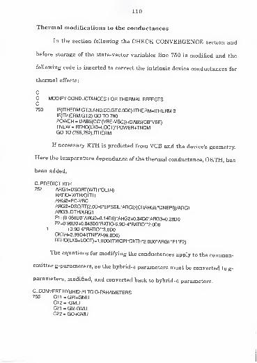
110
Thermal modifications to the conductances
In the section following the CHECK CONVERGENCE section and
before storage of the state-vector variables line 750 is modified and the
following code is inserted to correct the intrinsic device conductances for
thermal effects:
CC MODIFY CONDUCTANCES FOR THERMAL EFFECTSC750 IF(ITHERM.GT3.AND.CC.GT0.0D0) ITHERM=ITHERM-3
IF(ITHERM.GT2) GO TO 780POWER = DABS(CC*(VBE-VBC))+DABS(CB*VBE)TNEW = RTHO(LX0+LOCT)*POWER+TNOMGO TO (755,752), ITHERM
If necessary RTH is predicted from VCB and the device's geometry.
Here the temperature dependance of the thermal conductance, OKTH, has
been added,
C.PREDICT RTH752 ARG1 =DSQRT(WTH*OLTH)
RATIO=WTH/OLTHARG2=PC-VBCARG2=DSQRT(2.0D-6*EPSSIL*ARG2/(CHARGE*ONEPI))/ARG1ARG3=DTH/ARG1F1 =(0.058D0*ARG3+0.1 4D0)*ARG2+O.34D0*ARG3+O 28D0F2=0.98D0+0.043D0*RATIO-6.9D-4*RATIO"2 0D0
1 +3.9D-6*RATIO**3.0D0
OKTH=2.99D4/(TNEW-99.0D0)RTHO(LX0+LOCT)=1 .ODO/(TWOPI*OKTH*2.0DO*ARG1 *F1 *F2)
The equations for modifying the conductances apply to the common-
emitter g-parameters, so the hybrid-n parameters must be converted to g-
parameters, modified, and converted back to hybrid-n parameters.
C.CONVERT HYBRID-PI TO G-PARAMETERS755 G11=GPI4GMU
G12 = -GMUG21 = GM-GMUG22 = GO+GMU

Ill
TNEW is the temperature computed from the actual currents, not
the linearly predicted ones, TCB is the temperature coefficient of base
current with VBE held constant, and TCC is the temperature coefficient of
collector current with VBE held constant.
C.COMPUTE TEMPERATURE COEF.TIBE1 = (XTI+(EG-VBE/VALUE(LOCM+3))/VTT)ARG1 = BFM*CBEN/VALUE(LOCM+7)ARG2 = ARG1*(XTI-VALUE(LOCM+7)*XTB-VBE/VTT)TCB = ((TIBE1-XTB)*CBE-ARG2)/(TNEW*BFM*CB)TCC = TIBE1*(1 ODO-CC*OIK*Q1/DSQRT(1.0D044.0DO*CBE*OIK))/TNEW
Since the same equations hold in the ac analysis for the complex Y-
parameters, the unmodified values are saved. These electrical-only values
will be corrected in the ac matrix load routine, ACLOAD.f.
C..SAVE FOR AC ANALYSISVALUE(LOCV+4)=GPIVALUE(LOCV+5)=GMUVALUE(LOCV+€)=GMVALUE(LOCV+7)=GOVALUE(LOCV-fS)=TCBVALUE(LOCV+9)=TCC
Next the g-parameters are modified and converted back to hybrid-Ti
form.
CADJUST FOR THERMAL EFFECTSARGC = TCC * RTHO(LX0+LOCT)ARGB = TCB * RTHO(LX0+LOCT)DENC = 1 .0D0 - ARGC * POWERDENB = 1 .0D0 - ARGB * POWERGNUM1 1 = ARGB * CB * CBGNUM21 = CB * CCGNUM12 = ARGB *GNUM21GNUM21 = ARGC *GNUM21GNUM22 = ARGC * CC * CCG1 1 =(G1 1 +GNUM1 1 )/DENBG1 2=(G1 2+GNUM1 2)/DENBG21 =(G21 +GNUM21 )/DENCG22=(G22+GNUM22)/DENC
C.CONVERT BACK TO HYBRID-PI PARAMETERS 7GPI = G11 +G12GMU = -G12

112
GM = G21 -G12G0 = G22+G12
Changes for AC analysis
Changes to the ac analysis simulation code are similar to the
corrections to the conductances in the dc analysis. The only difference is
the conductances become complex admittances and the thermal resistance
becomes a complex thermal impedance, ZTH. The thermal impedance is
computed from the single-pole model ifCTH is specified on the model card.
Otherwise ZTH is computed from RTH using the point heat-source model.
Routine ACLOAD.f
The following code adds two new temperature dependancies: OKTH
is the thermal conductivity of silicon and OKAPPA is the thermal
diffusivity of silicon. Simple relations were used to approximate the
measured data for these variables [May67].
In the BJT section, check for a non-zero RTH in the state-vector and
for positive collector current.
GEPR=VALUE(LOCM+1 9)*AREAC.THERMAL MODEL
CC=VALUE(LOCT+2)RTH=VALUE(LOCT+20)IF(RTH.EQ.O.ODO.OR.CC.LE.O.ODO) GO TO 262CB=VALUE(LOCT+3)POWER=DABS(CC*(VALUE(LOCT)-VALUE(LOCT+1)))
+DABS(CB*VALUE(LOCT))TEMP=VALUE(LOCT+1 9)GPI=VALUE(LOCV+4)GMU=VALUE(LOCV+5)GM=VALUE(L0CV+6)GO=VALUE(LOCV+7)TCB=VALUE(LOCV+8)TCC=VALUE(LOCV+9)GO TO 263

113
If no thermal model,
262 GPI=...
Excess phase and imaginary parts of admittances,
263 XGM=...
270 GX=...
Modify admittances
C..THERMAL MODIFICATIONS TO ADMITTANCESIF(RTH.EQ.O.ODO.OR.CCLE.O.ODO) GO TO 280
C.CONVERT TO COMMON-EMITTER Y-PARAMETERSY1 1 =CMPLX(GPI-fGMU,XCMCB+XCPI+XCMU)Y12=CMPLX(-GMU,XCMCB+XCMU)Y21 =CMPLX(GM-GMU,XGM-XCMU)Y22=CMPLX(GO+GMU,XCMU)
Single-pole model,
IF (VALUE(LOCM+48).EQ.0.0D0) GO TO 273ZTH=CMPLX(RTH,VALUE(LOCM+48))GO TO 275
Computed from RTH using the temperature dependance of the
thermal conductance and diffusivity, OKAPPA [Nis80].
C.COMPUTE ZTH FROM RTH273 OKTH=2.99D2/(TEMP-99.0D0)
OKAPPA=OKTH*(TEMP-99.0D0)/(2.33D0*(TEMP-159.0D0))ARG1 =DSQRT(OMEGA/(2*OKAPPA))REFF=1 .0D0/(2.0D0*TWOPrOKTH*RTH)PHS=-REFF*ARG1OMAG=RTH*DEXP(PHS)ZTH=CMPLX(OMAG*DCOS(PHS),OMAG*DSIN(PHS))
Correct electrical-only admittances for self-heating,
C.MODIFY275 DENB=1 0D0/(1 .0D0-TCB*POWER*ZTH)
DENC=1 0D0/(1 0D0-TCC*POWER*ZTH)ARG1=CC*CBY1 1 =(Y1 1 +TCB*ZTH*CB*CB)*DENBY1 2=(Y1 2+TCB*ZTH*ARG1 )*DENBY21 =(Y21 +TCC*ZTH*ARG1 )*DENCY22=(Y22+TCC*ZTH*CC*CC)*DENC
C.CONVERT BACK TO HYBRID-PIGPI=REAL(Y1 1 )+REAL(Y1 2)GMU=-REAL(Y1 2)
GM=REAL(Y21 )-REAL(Y1 2)

114
GO=REAL(Y22)+REAL(Y1 2)
XGM=AIMAG(Y21 )+AIMAG(Y22)XCPI=AIMAG(Y1 1 )-AIMAG(Y1 2)
XCMU=AIMAG(Y22)XCMBC=AIMAG(Y1 2)-AIMAG(Y22)
Stuff into matrix as usual,
280 LOCY=LYNL+NODPLC(LOC+24) ...
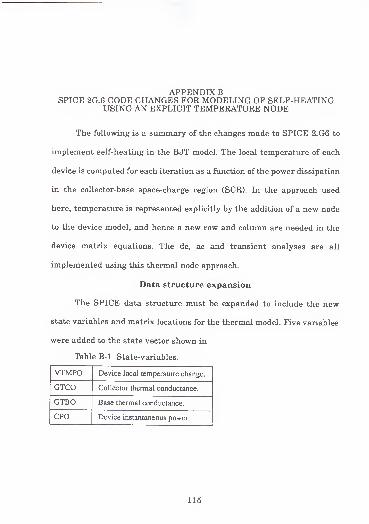
APPENDIX BSPICE 2G.6 CODE CHANGES FOR MODELING OF SELF-HEATING
USING AN EXPLICIT TEMPERATURE NODE
The following is a summary of the changes made to SPICE 2.G6 to
implement self-heating in the BJT model. The local temperature of each
device is computed for each iteration as a function of the power dissipation
in the collector-base space-charge region (SCR). In the approach used
here, temperature is represented explicitly by the addition of a new node
to the device model, and hence a new row and column are needed in the
device matrix equations. The dc, ac and transient analyses are all
implemented using this thermal node approach.
Data structure expansion
The SPICE data structure must be expanded to include the new
state variables and matrix locations for the thermal model. Five variables
were added to the state vector shown in
Table B-l State-variables.
VTMPO Device local temperature change.
GTCO Collector thermal conductance.
GTBO Base thermal conductance.
CPO Device instantaneous power.
115

116
Note: if more than a single-pole model is desired to model the
thermal response then an additional energy and energy-current state-
variable will be needed for each additional pole.
Subroutine Modifications
What follows is a quick description of the changes needed to each
routine to implement the thermal model. First the data structure must be
expanded to include the parameters described above. This includes eight
matrix locations and four state variables.
ADDELT
This routine adds an element and defines the size of linked-list
arrays for computation of offsets. Add eightelements to the matrix and one
variable to the device.
DATALNOD(12) = 38 LNOD(12) = 46LVAL(12) - 4 -* LVAL(12) = 5NNODS(12) = 4 -+ NNODS(12) = 5
ALTER
This routine changes the elements or device parameters for multiple
SPICE runs. Add eight elements to the matrix and one variable to the
device.
DATALNOD(12) = 38 LNOD(12) = 46LVAL(1 2) = 4 -+ LVAL(12) = 5
ELPRNT
In statement 300 change:
NODPLC(LOC+36) -» NODPLC(LOC+44)

117
ERRCHK
Add an external node to the BJT device line:
DATA NNODS(12) -4~+ NNODS(12) = 5
FIND
This routine presets storage for each input element. Add eight
elements to the matrix and one variable to the device.
DATALNOD(12) = 38 -* LNOD(12) = 46
LVAL(12) -4~* LVAL(12) = 5
MATLOC
In statement 830:
NODPLC(LOC+36) ~+ N0DPLC(L0C+44)
Then add new elements to matrix:
NODET=NODPLC(LOC436)
NODPLC(LOC+37)=INDXX(NODE4,NODET)NODPLC(LOC+38)=INDXX(NODE5,NODET)NODPLC(LOC+39)=INDXX(NODE6,NODET)NODPLC(LOC440)=INDXX(NODET,NODE4)NODPLC(LOC+41 )=INDXX(NODET,NODE5)NODPLC(LOC442)=INDXX(NODET,NODE6)NODPLC(LOC+43)=INDXX(NODET,NODET)
NODET is the external thermal node.
MATPTR
This routine builds the sparse matrix and it is here that the new
nodes are added.
In statement 530 change:
NODPLC(LOC+36) -» NODPLC(LOC+44)

118
Then add the new nodes and elements to the matrix:
NODET=NODPLC(LOC+36)CALL RESERV(NODE4,NODET)CALL RESERV(NODE5,NODET)CALL RESERV(NODE6,NODET)CALL RESERV(NODET,NODE4)CALL RESERV(NODET,NODE5)CALL RESERV(NODET,NODE6)CALL RESERV(NODET.NODET)
The offset for the LXI state-vector is increased by 4 (to make room
for state variables). In the section for the BJT matrix setup:
NXTRM=NXTRM+1 9 — NXTRM=NXTRM+23
MODCHK
This routine preprocesses device model parameters and prints out a
device summary. In statement 710 change:
NODPLC(LOC+36) -» N0DPLC(L0C+44)
then move the reference to the new external node:
NODPLC(LOC+36)=NODPLC(LOC+6)
READIN
This routine processes element and device model definitions.
DATAL2NOD(12) =36 -* L2NOD(12) =44
To read the external thermal node, above statement 306 change:
GO TO 308 GO TO 307
then after 306 add:
307 IF(NODPLC(ICODE+6).NE.0) GO TO 308IFLD=7
IF (NODPLC(LOC+L2NOD(ID)).NE.O) GO TO 309NODPLC(LOC-f€)=VALUE(IFIELD+6)GO TO 308
309 NODPLC(LOC+€)=0308 CONTINUE (no change)

119
The thermal node is temporarily placed in LOC+6 for reference in
TOPCHK and is moved to LOC+36 in the MODCHK routine
TOPCHK
Add external thermal node reference:
DATA NNODS(12) = 5
TRUNC
In statement 80 change:
NODPLC(LOC+36) -» N0DPLC(L0C444)
Changes for DC analysis
The following are changes needed for operating-point and dc-sweep
analysis. Here we have created a mirror BJT routine that is executed in
the event of a thermal analysis. This eliminates all of the "if thermal then
do this" statements that would otherwise be needed in the original BJT
routine. A drawback is the extra maintenance of a new model routine.
BJT
This routine performs the initialization, matrix load, voltage
limiting, and determines the operating point currents and derivatives for
the dc and transient analyses.
In the case of a thermal transistor branch to thermal version after
LOCM assignment:
IF (VALUE(LOC+36).NE.1 ) THENCALL BJTT(LOC)LOC=NODPLC(LOC)GO TO 10
ENDIF

120
BJTT
This routine performs the initialization, matrix load, voltage
limiting, and determines the operating-point currents and derivatives for
the dc and transient analyses for thermal transistors.
Add thermal resistance, temperature, thermal conductance, and
power current to the state-vector.
DIMENSION ...
3 VTMPO(1 ), GTCO(1 ), GTBO(1 ), CPO(1
)
EQUIVALENCE ...
7 (VTMPO(1 ),VALUE(20)). (GTCO(1 ),VALUE(21 )), (GTBO(1 ),VALUE(22)),
8 (CPO(1),VALUE(23))
then add the new node:
NODET=NODPLC(LOC+36)
Set the power to zero:
CP=0.0D0
In the DC model parameters section some additional variables need
to be denned:
PC=VALUE(LOCM+30)XTB=VALUE(LOCM+41)EG=VALUE(LOCM-f42)XTI=VALUE(LOCM+43)VTT=VT (so Vt can vary with each device's temperature)
TNOM=VALUE(ITEMPS+ITEMNO)+CTOK
Note: The nominal temperature is referenced as
VALUE(ITEMPS+ITEMNO)+CTOK in Kelvin. It is always the current
ambient temperature whether it is the default temperature, .TEMP value,
or TNOM value.

121
Initialize temperature flag (used to indicate wether device is in the
proper region of operation for thermal iteration):
NOTMP=. FALSE.
Initialization section
After statement 25 (INITF = 2) insert:
VTMP=0.0D0
This initializes the temperature to the ambient.
If the device is off there is no power dissipated. After statement 40
(INITF = 3) insert:
VTMP=0.0D0
After statement 50 (INITF=4):
VTMP=VTMPO(LX0+LOCT)IF (VBC.GT.0.0D0) NOTMP=.TRUE.
After statement 60 (INITF=5):
VTMP=VTMPO(LX1 +LOCT)IF (VBC.GT.0.0D0) NOTMP=.TRUE.
After statement 70 (INITF=6):
IF (VBC.GT.0.0D0) NOTMP=.TRUE.VTMPO(LX0+LOCT)=vTMPO(LX1 +LOCT)vTMP=(1.0D0+XFACT)*VTMPO(LX1+LOCT) - XFACT*VTMPO(LX2+LOCT)GTCO(LX0+LOCT)=GTCO(LX1 +LOCT)GTBO(LX0+LOCT)=GTBO(LX1 +LOCT)
After statement 100 (INITF=1), normal iteration:
IF (VBC.GT.0.0D0) NOTMP=.TRUE.VTMP=VALUE(LVNIM1 +NODET))
and after statement 110:
DELVTMP=VTMP-VTMPO(LX0+LOCT)CCHAT=CCO(LX0+LOCT)+(GMO(LX0+LOCT)+GOO(LX0+LOCT))*DELVBE

122
1 -(GOO(LX0+LOCT)+GMUO(LX0+LOCT))*DELVBC4GTCO(LX0+LOCT)*DELVTMPCBHAT=CBO{LX0+LOCT)+GPIO(LX0+LOCT)*DELVBE4GMUO(LX0+LOCT)*DELVBC
1 4GTBO(LX0+LOCT)*DELVTMP
If not forward active, set power to zero:
IF (NOTMP) THENCPHAT=0.0D0ELSECPHAT=CPO(LX0+LOCT)+DABS(CCO(LX0+LOCT)*DELVCE)
1 +DABS(CBO(LX0+LOCT)*DELVBE)ENDIF
Add a convergence check for the temperature in the last position of
the BYPASS IF SOLUTION HAS NOT CHANGED section:
TOL=RELTOL*DMAX1 (DABS(VTMP),DABS{VTMPO(LX0+LOCT)))+VNTOL*1 D2IF (DABS(DELVTMP).GE.TOL) GO TO 200
This avoids premature convergence in dc sweeps before the
temperature has settled. After this add the lines:
VTMP=VTMPO(LX0+LOCT)GTC=GTCO(LX0+LOCT)GTB=GTBO(LX0+LOCT)CP=CPO(LX0+LOCT)
Update of temperature-dependent variables
Temperature-dependent model parameters IS, ISE, ISC, BF, BR,
EG, and VT are recomputed to reflect the local temperature increase. The
following statements were added after the LIMIT NONLINEAR BRANCH
VOLTAGES section:
210 CONTINUEIF (VTMP.LTO.ODO) THEN
VTMP=0.0D0NOTMP=.TRUE.
ELSELOOPTMP=.TRUE.DELTMP=1 D-1
ODELTMP=1D1VTMP=VTMP+DELTMP
ENDIF220 CONTINUE

123
DTEMP=VTMP/TNOMRATI0=DTEMP+1 .ODO
RATLOG=DLOG(RATIO)TLOC=TNOM+VTMPVTT=BOLTZ*(TLOC)/CHARGEEG=EGO-(EGAP*TLOC*TLOC)/(TLOC+TGAP)FACTLN=DTEMP*EGA/TT+XTI*RATLOGFACTOR=DEXP(FACTLN)CSAT=VALUE(LOCM+1 )*AREA*FACTORBFACTR=DEXP(XTB*RATLOG)BFM=VALUE(LOCM+2)*BFACTRBRM=VALUE(LOCM+8)*BFACTRC2=VALUE(LOCM+€)*AREA*DEXP(FACTLhWALUE(LOCM+7))/BFACTRC4=VALUE(LOCM+12)*AREA*DEXP(FACTLNA/ALUE(LOCM+13))/BFACTR
These equations are equivalent to those in the temperature update
routine, TMPUPD. Note: VTT is the new thermal voltage, and VT should
be replaced by it throughout this subroutine.
Computation of the new conductance and current terms
The thermal model is valid only in the forward-active region, so
should only be computed in this case. If the device is not in the forward-
active region then temperature coefficients will be zero. The thermal
transconductance is computed in the DETERMINE DC INCREMENTAL
CONDUCTANCES section before statement 440:
IF (NOTMP) THENCP=0.0D0GTB=0.0D0GTC=0.0D0
ELSE IF (LOOPTMP) THENCPHI=DABS(VCE*CC)+DABS(VBE*CB)CCHI=CCCBHI=CBCC=0.0D0LOOPTMP=. FALSE.VTMP=VTMP-DELTMPGOTO 220
ELSECP=DABS(VCE*CC)+DABS(VBE*CB)GTC=(CCHI-CC)*ODELTMPGTB=(CBHI-CB)*ODELTMP

124
ENDIF
Check convergence
After statement 700, add a convergence check for power:
TOL=RELTOL*1 .0D3*DMAX1 (DABS(CPHAT),DABS(CP))+ABSTOLIF (DABS(CPHAT-CP).LE.TOL) GO TO 780
Load the matrix
Save the state vector information:
VTMPO(LX0+LOCT)=VTMPGTCO(LX0+LOCT)=GTCGTBO(LX0+LOCT)=GTBCPO(LX0+LOCT)=CP
Compute and store the currents:
900 CEQBE=TYPE*(CC+CB-VBE*(GM4GO-fGPI)+VBC*(GO-GEQCB)1 -VTMP*(GTC+GTB))
CEQBC=TYPE*(-CC+VBE*(GM4GO)-VBC*(GMU4GO)+VTMP*GTC)... (to the end of section)
IF(.NOT.NOTMP) THENVALUE(LVN+NODET)=VALUE(LVN+NODET)+{CP-VCE*(VCE*GO+VBE*GM
1 +vTMP*GTC*TYPE)-VBE*(VBE*GPI+VTMP*GTB*TYPE))ENDIF
Stuff the conductance matrix:
950 ... (to the end of normal load)
LOCY=LVN+NODPLC(LOC+37)VALUE(LOCY)=VALUE(LOCY)+GTC*TYPELOCY=LVN+NODPLC(LOC+38)VALUE(L0CY)=VALUE(L0CY)4GTB*TYPELOCY=LVN+NODPLC(LOC+39)VALUE(LOCY)=VALUE(LOCY) - (GTC+GTBJTYPELOCY=LVN+NODPLC(LOC+40)VALUE(LOCY)=VALUE(LOCY)-VCE*GO*TYPELOCY=LVN+NODPLC(LOC+41
)
VALUE(LOCY)=VALUE(LOCY)-(VCE*GM+VBE*GPI)*TYPELOCY=LVN+NODPLC(LOC+42)VALUE(LOCY)=VALUE(LOCY)+(VCE*(GM4GO)+VBE*GPI)*TYPELOCY=LVN+NODPLC(LOC+43)VALUE(LOCY)=VALUE(LOCY)-(GTC*VCE4GTB*VBE)*TYPE
1000 RETURNEND

125
Output of operating-point information
DCOP
This routine prints out operating-point information. The following
changes allow thermal resistance, local temperature increase, and
thermal conductance to be printed in response to the .OP command.
DIMENSION2 CCS(12), CBX(12), RX(12),DTMP(12), GTC(12), GTB(12)
DATA ADTMR GTMP / 5HDELT, 3HGTC, 4HGTB /
Change BJT section:
In statement 320 and in the statement after 360 change:
NODPLC(LOC+36) — NODPLC(LOC-f44)
then add:
BETADC(KNTR)=CC(KNTR)/DSIGN(DMAX1 (DABS(CB(KNTR)),1 .OD-20),
1 CB(KNTR))DTMP(KNTR)=VALUE(LOCT+1 9)
GTC(KNTR)=VALUE(LOCT+20)GTB(KNTR)=VALUE(LOCT+21
)
IF (MODEDC.NE.1) GO TO 325
IF (VALUE(LOCT+19) .EQ. 0.0D0) GO TO 355WRITE (IOFILE.AFMT2) ADTMP,(DTMP(I),I=1,KNTR)WRITE (IOFILE.AFMT2) AGTC,(GTC(I),I=1,KNTR)WRITE (IOFILE.AFMT2) AGTB,(GTB(I),I=1 ,KNTR)
355 IF (MODEDC.NE.1) GO TO 360
These thermal variables are printed only if a thermal model is used.
Changes for AC analysis
Changes to the ac analysis simulation code are similar to the
corrections to the change in the dc analysis.

126
ACLOAD
In the BJT section, change the end of linked-list check:
260 IF ((LOC.EQ.O).OR.(NODPLC(LOC+44).NE.O)) GO TO 300
After the other admittance terms have been loaded the following
code is added for the thermal model:
IF(NODPLC(LOC+36).NE.1) THENGTC=VALUE(LOCT+20)GTB=VALUE(LOCT+21)VBE=VALUE(LOCT)VCE=VALUE(LOCT)-VALUE(LOCT+1
)
CC=VALUE(LOCT+2)LOCY=LYNL+NODPLC(LOC+37)VALUE(LOCY)=VALUE(LOCY)4GTCLOCY=LYNL+NODPLC(LOC+38)VALUE(LOCY)=VALUE(LOCY)+GTBLOCY=LYNL+NODPLC(LOC+39)VALUE(LOCY)=VALUE(LOCY)-(GTC4GTB)LOCY=LYNL+NODPLC(LOC+40)VALUE(LOCY)=VALUE(LOCY)-VCE*(GO+GMU)-CCL0CY=LYNL+N0DPLC(L0C+41
)
VALUE(LOCY)=VALUE(LOCY)-VCE*(GM-GMU)-VBE*GPI-CBLOCY=LYNL+NODPLC(LOC+42)VALUE(LOCY)=VALUE(LOCY)+VCE*(GM+GO)+VBE*GPI+CC+CBLOCY=LYNL+NODPLC(LOC+43)VALUE(LOCY)=VALUE(LOCY)-GTC*VCE-GTB*VBEENDIF
Table B-2 Offsets for BJT matrix elements.
LOC c B E c b e s ^extC 24 10
B 25 34 11
E 26 12
c 13 35 27 14 15 32 37
b 16 17 28 18 38
e 19 20 21 29 39
s 33 31TAext 40 41 42 43
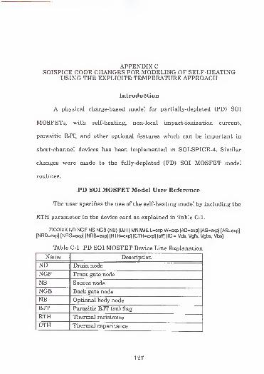
APPENDIX CSOISPICE CODE CHANGES FOR MODELING OF SELF-HEATING
USING THE EXPLICITE TEMPERATURE APPROACH
Introduction
A physical charge-based model for partially-depleted (PD) SOI
MOSFETs, with self-heating, non-local impact-ionization current,
parasitic BJT, and other optional features which can be important in
short-channel devices has been implemented in SOI-SPICE-4. Similar
changes were made to the fully-depleted (FD) SOI MOSFET model
routines.
PD SOI MOSFET Model User Reference
The user specifies the use of the self-heating model by including the
RTH parameter in the device card as explained in Table C-l.
ZXXXXX ND NGF NS NGB (NB) (BJT) MNAME L=exp W=exp [AD=exp] [AS=exp] [AB=exp][NRD=exp] [NRS=exp] [NRB=exp] [RTH=exp] [CTH=exp] [off] [IC = Vds, Vgfs, Vgbs, Vbs]
Table C-l PD SOI MOSFET Device Line Explanation
Name Description
ND Drain node
NGF Front gate node
NS Source node
NGB Back gate node
NB Optional body node
BJT Parasitic BJT (on) flag
RTH Thermal resistance
CTH Thermal capacitance
127

128
PD SOI MOSFET Model Implementation
The following figure shows how current and voltage are used as
duals to power dissipation and temperature. The power of the device is
applied as a current that generates a voltage as it flows through the
thermal impedance, RTH and CTH, that is equivalent to the change in
temperature of the device. The increase in temperature is used to update
the device model parameters each iteration. If the parameter RTH is not
specified on the device line, the above thermal subcircuit is not generated,
and the standard isothermal model is used. The changes in SPICE2G.6
files made to implement self-heating in the PD SOI MOSFET model are
marked with "Cdtz" comments in the Fortran source code. The
implementations required changes to 17 subroutines and the addition of
one new routine, all described below.
Subroutines ADDELT and ALTER
In these routines the matrix size defined by LNOD(16) was
increased by 1 2 for the new admittance matrix elements.
Subroutine FIND
This routine checks for repeated element names and allocates
memory for unique elements. The matrix size defined by LNOD(16) was
increased by 12 for the new admittance matrix elements. Also, the
IFORCE argument value of two is added to bypass the repeated name
check. This is needed to allocate memory for the thermal capacitance,

129
since all thermal capacitors have the same name. This is explained in the
MODCHK section.
Subroutine READIN
This routine decodes the input deck. First L2NOD(16) is increased
by 12 for thermal elements of the admittance matrix. The device line
parameters RTH and CTH were added to the list.
Subroutine MODCHK
This routine processes the model parameters. In the NFD section
where the parasitic resistances are added, check for RTH, add the
temperature node to the matrix, and add the CTH capacitor if needed.
IF (VALUE(LOCV+25).NE.0.0D0) THENNUMNOD=NUMNOD+1NODPLC(LOC+47)=NUMNODVALUE(LCX)V+25)=1.0D0/VALUE(LOCV+25)IF (VALUE(LOCV+26).NE.0.0D0) THENCALL FIND(ACGATOR,2,LOCTH,2)LOCvTH=NODPLC(LOCTH+1
)
NODPLC(LOCTH+2)=NUMNODNODPLC(LOCTH+3)=1VALUE(LOCVTH+1 )=VALUE(LOCV+26)NODPLC(LOCTH+4)=1
ENDIFELSE
NODPLC(LOC+47)=1ENDIF
All the thermal capacitors are added to the normal capacitor list
with the name GATOR; this name was chosen arbitrarily. FIND is forced
to bypass the name-checking by the 2 in the call (see above).

130
Subroutines MATPTR and MATLOC
These routines reserve memory for the linked list. The thermal
matrix elements and state variables are added as shown in the linked list
provided at the end of this document.
Subroutine NFDFET
This subroutine, by calling NFDID and NFDEC, performs the
initialization, matrix-load operations, and voltage-iterate limiting, and
determine the operating-point currents and charges and their respective
derivatives for the PD SOI MOSFET device. The following is a description
of the thermal changes relating to self-heating.
Make a new common block for thermal arguments (used for FD
devices also):
COMMON /TMPARG/ GMTMRGIITMRGIRTMP.GITTMP.GPWFiTMP.GPWRGF.GPWRDS,& GPWRGB.GPWRBY.GD.GS
Extend dimension and equivalence for the thermal state-variables. Get
temperature node (this will be a flag for temperature modeling).
NTMP=NODPLC(LOC447)
Variables VTMP (temperature change) and CPWR (power
dissipation) are treated the same as any other voltages and currents. The
temperature change is limited to positive values. Add thermal arguments
to NFDID call for normal and inverse modes:
CALL NFDID(VGFS,VDS,VGBS,VBS,LOC,QD,QGF,QS,QGB,QBY&
& CBD,CBGB,CBS,CDGB,CSGB,CGBD,VTMP,CPWR,CPWRTMP& CGFTMPCDTMPCGBTMP.CBYTMPCSTMP)

131
In the transient analysis, add thermal parameters to NFDEC call
and include in tranconductance computations for normal and inverse
modes:
CALL NFDEC(VGFD,VGFS,VGFB,VGBD>VGBS,VGBB,XNQFF,XNQFB,
&& CDTMP.CSTMP.CGFTMP.CGBTMP.CBYTMRGCDTMP.GCSTMRGCGFTMR& GCGBTMRGCBYTMP)GCGFS=-(GCGFGF+GCGFD+GCGFB+GCGFTMP)GCDS=-(GCDGF+GCDD-fGCDB+GCDGB4GCDTMP)GCBS=-(GCBGF+GCBD+GCBB+GCBGB+GCBYTMP)GCGBS=-(GCGBB+GCGBD+GCGBGB+GCGBTMP)GCSS=-(GCSGF+GCSD-tGCSB+GCSGB+GCSTMP)
Conditionally compute current-vector element for power and add
temperature parameters to other vector elements for normal and inverse
modes, and load power element of current vector. Also check if drain and
source resistances need updating:
IF (NTMP.NE.1) THENVALUE(LVN+NTMP)=VALUE(LVN+NTMP)+CPWREQIF (VTMPGT.O.ODO) THENGDPFM3DGSPR=GSENDIF
ENDIF
Load thermal elements of the admittance matrix.
Subroutine NFDID
This subroutine, by calling NFDMOD, numerically calculates the
derivatives of the operating-point currents and charges for both the
forward and inverse modes of operation of the NFD/SOI device. The same
changes to the common block and subroutine arguments done for NFDFET
are repeated here. An additional call to NFDMOD is made to find the
temperature derivatives.

132
Subroutine NFDEC
This subroutine calculates the transcapacitance terms used in
transient and AC analysis from the intrinsic and extrinsic components of
charge in the NFD/SOI device. Thermal transient conductance terms are
also computed in this routine.
Subroutine NFDMOD
This subroutine, the primary model routine, calculates the channel
transport, impact-ionization, junction leakage, and if requested the
parasitic bipolar transistor currents of the PD SOI MOSFET for the given
internal device voltages, as well as the intrinsic charge components that
define the charging currents. After the model parameters are loaded and
before any computations are made, SOITMP is called to update the
temperature dependent parameters for the local temperature. The local
thermal voltage VTT is substituted everywhere the global thermal voltage
VT was used.
It is important to assign the model parameter values to local
variables before the SOITMP call and not to directly access the model
parameter values (e.g. VALUE(LOCM+?)) in subsequent calculations.
Otherwise these model parameters would not reflect changes in local
temperature, which could cause inaccurate results.

133
Subroutine SOITMP
This subroutine updates all of the temperature dependent
parameters for each device on each iteration. It is called by the NFDMOD
routine. The parameters affected are shown in Table C-2.
Table C-2 Temperature dependent parameters.
NAME Description
XNIN Intrinsic carrier density
EGFET Silicon energy gap
VTT Local Thermal Voltage
YMT TT r»C2 T LDD carrier mobility
YMT TRT-T Minority earner mobility in high-doped
body
uo Zero field electron mobility
VSAT Carrier saturated drift velocity
WKF Front-gate work function difference
WKB Back-gate work function difference
VFBF Front-gate flatband voltage
VFBB Back-gate flatband voltage
JRO Body-source junction recombinationcurrent coefficient
ALPHA Impact-ionization parameter a0TAUG Carrier lifetime in lightly doped region
VBI Source to bulk built-in potential
PHIB Twice fermi potential of body
RLDD LDD sheet resistivity
BETA b
FSAT fsat
GD Drain parasitic resistance
GS Source parasitic resistance
These are the same dependencies used in TMPUPD implemented by
Glen Workman [Wor96]. If temperature dependencies are changed or
added to TMPUPD, corresponding changes must also be made to SOITMP.

134
Subroutine DCOP
This routine generates the output for the operating point. If self-
heating is modeled for a device, the change in temperature, power
dissipated, and relevant conductance and capacitance terms are printed.
Subroutine ACLOAD
This routine loads the complex admittance matrix for the ac
analysis. If there is a device with self-heating, the thermal elements of the
matrix are loaded. See description of NFDFET routine.
Data Structures
The data structures for the PD SOI MOSFET device (ID=16) and
model (ID=26), and for the print (ID=41) and plot (ID=42) are given in
Table C-3 for SOI-SPICE-4.3i. All other linked lists remain the same as in
the original SPICE2G.6.
Table C-3 Offsets for PD SOI MOSFET matrix elements.
LOC D Gf S Gb B d s b TD 38 13
Gf 39 14 15 16 49
S 40 17
Gb 41 18 19 20 50
B 42 21
d 22 23 24 43 25 26 51
s 27 28 29 30 44 31 52
b 32 33 34 35 36 45 53
T 54 55 56 57 58 48

135
PD SOI MOSFET Transistor (ID=16)
U 1 : subckt info
i +nn: next pointer LOCV +00:
~U 1•
i nrvLUvV +nrTUZ 1 lvJ +n9-
: ngf +ni-+Uo.+(\A'U4 nelib +(14-
+U5 nyu +n^-+UO.
+UO nhriQ +nA-
+fl7+U/ nap +n7-
+UO nsp +nA-+UO.
nbp +no-
+ 1 n1 1 icxjtri poimer + in-+ IU.
4-11 UIT + i i•
+ 19+ 1 z + 19-
4-1 7T1 O tna,nap; + 1 *+ lo.
+ 1/1 + 1 /!•
+ 1CT IO + Tv+ 1
A
T1
0
t'nof nhn^viyMiup/ + 1 A-T 1 0.
+ 17V1 'b
,I IdfJJ + 17-
+ lft' 1 o wiyujiup; + 1 ft-
+ 10 f'nnh ncr^• ingu.nsp/ ^ i y.
+9n uigD.nDp; +9n-+ZU.+91 vnD.nDp; +91 •+z l
.
+99 map,na; +ZZ.+91+ZO . (nap.ngf) +23:
+Z4 (nap.ngo) +z4:
+Z5 inap.nsp; i Of .
+OA+ZO (nap.nDp; +ZO.+97 uisp.nyT; +97-
+9A vnsp,nsj +9A-+ZO.+90 insp.ngo; +90-+ZT.
inspjiup;+^1
+^9 fnKn norf\inup,ngi;
+13 /nhn n/"ir™^Uiup,nyu;+\4To4 (nup.nD; +4o:+m Wiup,n<jp; +4y:
(nDp.nsp) i en.+50:+17-
LXI Onset +51:4. OQ+«Jo. ina,na) +52:+io- (ngf.ngf) +53:T4U. (ns.ns) +54:
+41: (ngb.ngb) +55:+42: (nb.nb) +56:+43: (ndp.ndp) +57:
+44: (nsp.nsp) +58:
+45: (nbp.nbp)+46: body mode (0 for float.)
device namechannel length L
channel width WIC - vds
IC - vgfs
IC - vgbsIC - vbs
DEVMODADASABGD (NRD)
GS (NRS)
GB (NRB)
BETA (MODCHK)FSAT (MODCHK)DICEFAC (MODCHK)XLMODFAC (MODCHK)RLDD (MODCHK)COVLGFDCOVLGFSCOVLGFB<unused><unused>COVLGBBRTH
CTH<unused><unused><unused>
nt
(nt.nf)
(ngf.nt)
(ngb.nt)
(ndp.nt)
(nsp.nt)
(nbp.nt)
(nt.ngO
(nt.ngb)
(nt.ndp)
(nt.nsp)
(nt.nbp)
136
PD SOI MOSFET Model (ID=26)
-01: subcktinfo
+00: next pointer LOCM +00: model name+01: LOCM +01: VFBF+02: model tvDe +02: VFBB
+03: TOXF+04: TOXB+05: WKF+06: WKB+07: NQFF+08: NQFB+09: NSUB+ 10: NGATE+ 11: FNK+12: FNA+13: TF
+14: TB
+15: THALO+ 16: NBL+ 17: NBH+ 18: NHALO+ 19: UO+20: THETA+21: VSAT+22: TPG+23: TPS
+24: NLDS+25: NDS+26: LLDS
+27: HDD+28: LDIFF
+29: ZETA
+30: ETA+31: LMOD+32: ALPHA+33: BETA+34: BFACT+35- CGFDO+36- CGFSO+37: CGFBO+38: RD+39: RS
+40: RB+46: JRO +41: TAUO+47: M +42: DL+48: VJMIN +43: DW+49: unavailable +44: RHOSD+50: FVBJT +45: RHOB
State Variable Table (PD SOI MOSFET Model)Lxi+00: vbso(VBS)
+01: vbdo(VBD)+02: vgfso(VGFS)

137
+03 : vgfdo(VGFD)+04 : vgbso (VGBS)+05 : vdso (VDS)
+06 : cicho(ICH)+07 : ciro OR)
+08 : cigto (IGT)
+09 : cigioOGI)+ 10 : cbjto(IBJT)
+ 11 : gidgfso (GDGF)+ 12 : giddso(GDO)+ 13 : gidbso (GDB)+ 14 : giigfso (GGIGF)+ 15 : giidso (GGID)+ 16 : giibso (GGIB)+ 17 : girbso GRB)+ 18 : qdo(QD)+ 19 : cqdo (IQD)
+20 : qgfo (QGF)+21 : cqgfo (IQGF)
+22 : qso (OS)
+23 : cqso (IQS)
+24 : qgbo (QGB)+25 : cqgbo (IQGB)+26 qbo(QB) +49 : vtwo+27 : cqbo (IQB) +50 : vdsato+28 cdgfo +51 : vdsato+29 cddo +52 : leffo
+30 cdbo +53 cgbdo+31 cdso +54 cdgbo+32 cgfgfo +55 csgbo+33 cgfdo +56 qno+34 cgfbo +57 vtmpo (temperature)
+35 cgfso +58 cpwro (power)+36 csgfo +59 gmtmpo+37 csdo +60 giitmpo+38 csbo +61 girtmpo+39 csso +62 cgttmpo+40 cgbgbo +63 cdtmpo+41 cgbbo +64 cstmpo+42 cgbso +65 cgbtmpo+43 cbgfo +66 cbytmpo+44 cbdo +67 gpwrtmpo+45 cbgbo +68 gpwrgfo+46 cbbo +69 gpwrdso+47 cbso +70 gpwrgbo+48. vtso +71 gpwrbyo
Comments (PD SOI MOSFET Model):
"Model Type" is +1 for NNFDSOI and -1 for PNFDSOI.
The following preprocessing is performed in subroutine MODCHK:
Location: Stored Term:

138
LOCM+NZPARAM+l
LOCM+NZPARAM+2
LOCM+NZPARAM+3LOCM+NZPARAM+4
LOCM+NZPARAM+5LOCM+NZPARAM+6LOCM+NZPARAM+7LOCM+NZPARAM+8LOCM+NZPARAM+9LOCM+NZPARAM+10LOCM+NZPARAM+l 1
LOCM+NZPARAM+l 2
LOCM+NZPARAM+l 3
LOCM+NZPARAM+14
LOCM+NZPARAM+l 5
LOCM+NZPARAM+l 6
LOCM+NZPARAM+l 7
LOCM+NZPARAM+l 8
LOCM+NZPARAM+l 9
VBI (S-B built-in potential)
CB=EPSSIL/TB
COXF=EPSOX/TOXF
COXB=EPSOX/TOXB
QB=-CHARGE*TB*NBL
PHIB=2"VT-DLOG(NBL/NI)
TLDD=TF-THALO
XALPHA=l+CB/COXF
XLC=TB( CB/(2*COXF*XALPHA)) l/2
<unused>
<unused>
<unused>
XMUBH (minority-carrier mobility
in high-doped body)
<unused>
(unused>
ESLOPE=CHARGE*NLDS/EPSSIL
TAUG=2*TAUO/(l +NBL/NO)
XMOBFAC1 =THETA*COXF/(2*EPSSIL)
XBFACT=BFACT"XMOBFACl /
(2-XALPHA)
Note: NZPARAM=50 for current number of input parameters.
Additional COMMON blocks:
COMMON /NFDARG/ CICH.CIR.CIGT.CIGI.CBJT.GIDGFS.GIDDS.GIDBS,
GIIGFS,GIIDS,GIIBS,GIRBS,VTS,VTW,XLEFF,VDSAT
COMMON /TMPARG/ GMTMRGIITMRGIRTMRGITTMRGPWRTMP,GPWRGF.GPWRDS.GPWRGB.GPWRBY

139
Output Variables (IP=41.42)
-01 subckt info
LOC+00 next pointer LOCV +00: Element Name+01 LOCV +01: Device Name+02 Device ID / LOC +02: Oper Var Name+03 KOFF (LOCT/LOCV offset)
+04 ISEQ
+05 type=9+06 KLOC (KLOCT/KLOCV offset)
+07 ISTATE (S=0, P=l)
Comments:For ID=41,42 and type (NODPLC(LOC+5)) = 0, 1, and 2-8, the definitions
of the variables remain as defined in the "Program Reference for SPICE2".

APPENDIX DSPICE CIRCUIT DESCRIPTIONS USED FOR SIMULATION
EXAMPLES
Single BJT Common-Emitter Amplifier
This is a single NPN common-emitter amplifier circuit with an open-
circuit load used to generate Figure 4-1.. Dc operating point and ac
analyses are executed.
COMMON-EMITTER AMPLIFIER CIRCUITVBE 2 0 .82 AC 1
VCE 1 0 5
LT1 3 1GQ1 3 2 0 0 4H3X50NXZTH 4 0 ZTH*Three-pole Model
.SUBCKT ZTH 1 4RTH1 1 2 92.4
CTH1 1 2 1 .02u
RTH2 2 3 142.8
CTH2 2 3 0.187U
RTH3 3 4 44.8
CTH3 3 4 55.6n
.ENDS*
.MODEL H3X50N NPN (IS=1 .875E-16 XTI=3 EG=1.16 VAF=60 VAR=4.5+ BF=146.1 ISE=1.875E-19 NE=1.4 IKF=7.5E-2 XTB=2 BR=10+ ISC=1.875E-14 NC=1.8 IKR=7.5E-2 RC=29.4 CJC=2.818E-13+ MJC=0.24 VJC=0.97 FC=0.5 CJE=3.9E-13 MJE=0.51 VJE=0.872+ TR=4E-9TF=17.85E-12 ITF=1 .155 XTF=78.81 VTF=10 PTF=0+ XCJC=0.1756 CJS=1.689E-13 VJS=0.75 MJS=0 RE=1.333 RB=35.18+ RBM=0 KF=0 AF=1 EGAP=7.02E-4 TGAP=1 108)'Simulation Section
.OPTIONS NUMDGT=7 LIMPTS=2000 RELTOL=1 e-5 ITL1=1000 ITL2=1000
.WIDTH OUT=80
.OP
.AC DEC 5 1 1G
.PRINT AC V(3)
.END
140

141
741 Operational Amplifier Circuit
This is the 741 operational amplifier found in Grey and Meyer
[Gra84]. The schematic in shown in Figure 4-2, and the simulation results
and shown in Figures 4-3 and 4-4. Dc operating point, dc transfer and ac
analyses are executed.
SELF-HEATING 741 OP-AMP CIRCUITVCC 1 0 DC 15
VEE6 0DC-15VI1 8 0DC0VI2 9 0 DC .835M AC 1
R1 1561KR2 16 61KR3 14 6 50KR4 5 6 5KR5 2 3 39KR6 24 25 27
R7 25 26 22
R8 20 6100R9 19 6 50KR10 22 23 40KCC1317.65PQ1 7 8 10 6 51 H3x50N02 7 9 11 6 52 H3x50NQ3 12 4 101 53 H3x50PQ4 13 411 1 54H3x50PQ5 12 1415 6 55H3x50NO6 13 14 16 6 56 H3x50NQ7 1 12 14 6 57H3x50NQ8 7 7 1 1 58 H3x50PQ9 4 7 1 1 59 H3x50PQ104 3 5 660H3X50NQ1 1 3 3 6 6 61 H3x50NQ1222 1 1 62 H3x50PQ13A21 2 1 1 63 H3x50P .25
Q13B17 2 1 1 64H3x50P.75Q141 21 24 6 65 H3x50NQ161 13 19 6 66 H3x50NQ17 17 19 20 6 67 H3x50NQ18 21 22 23 6 68 H3x50NQ1 9 21 21 22 6 69 H3x50N020 6 23 26 1 70 H3x50PQ23A6 17 23 1 73 H3x50PXZTH1 51 0 ZTHXZTH2 52 0 ZTHXZTH3 53 0 ZTHXZTH4 54 0 ZTH

142
741 op-amp circuit continued.
XZTH5 55 0 ZTHXZTH6 56 0 ZTHXZTH7 57 0 ZTHXZTH8 58 0 ZTHXZTH9 59 0 ZTHXZTH10 60 0 ZTHXZTH1 1 61 0 ZTHXZTH12 62 0 ZTHXZTH13 63 0 ZTHXZTH14 64 0 ZTHXZTH15 65 0 ZTHXZTH16 66 0 ZTHXZTH17 67 0 ZTHXZTH18 68 0 ZTHXZTH19 69 0 ZTHXZTH20 70 0 ZTHXZTH23 73 0 ZTH*Three-pole Model
.SUBCKT ZTH 1 4RTH1 1 2 92.4
CTH1 1 2 1 .02u
RTH2 2 3 142.8
CTH2 2 3 0.187U
RTH3 3 4 44.8
CTH3 3 4 55.6n
.ENDS*
.MODEL H3X50N NPN (IS=1.875E-16 XTI=3 EG=1.16 VAF=60 VAR=4.5+ BF=146.1 ISE=1.875E-19 NE=1.4 IKF=7.5E-2 XTB=2 BR=10+ ISC=1.875E-14 NC=1.8 IKR=7.5E-2 RC=29.4 CJC=2.818E-13+ MJC=0.24 VJC=0.97 FC=0.5 CJE=3.9E-13 MJE=0.51 VJE=0.872+ TR=4E-9 TF=17.85E-12 ITF=1.155 XTF=78.81 VTF=10 PTF=0+ XCJC=0.1756 CJS=1.689E-13 VJS=0.75 MJS=0 RE=1.333 RB=35.18+ RBM=0 KF=0 AF=1 EGAP=7.02E-4 TGAP=1108)*
.MODEL H3X50P PNP (IS=1.02E-16 XTI=3 EG=1.16 VAF=30 VAR=4.5+ BF=70.11 ISE=1.02E-19 NE=1.4 IKF=7.5E-2 XTB=2 BR=7+ ISC=1.02E-14 NC=1.8 IKR=7.5E-2 RC=38 CJC=4.27E-13+ MJC=0.3 VJC=1 .23 FC=0.5 CJE=4.8E-13 MJE=0.57 VJE=0.88+ TR=4E-9 TF=33.91E-12 ITF=0.7127 XTF=45.14 VTF=10 PTF=0+ XCJC=0.1756 CJS=1.689E-13 VJS=0.75 MJS=0 RE=1.333 RB=37.4+ RBM=0 KF=0 AF=1 EGAP=7.02E-4TGAP=1108)•Simulation Section
.OPTIONS NUMDGT=7 TNOM=25 ACCTOP.DC VI2 0 3m 10u.AC DEC 5 1 100meg.PRINT DC V(25)
.PRINT AC VM(25)END

143
Pin-Driver Transient
This is the pin-driver circuit to demonstrate the transient effects of
self-heating. The schematic for this circuit is shown in Figure 4-5, and the
results are shown in Figures 4-6 and 4-7.
•THERMAL PIN-DRIVER CIRCUITVIN 3 2 5 pulse (2 18 1u 5n 5n 500u 1000u)
Q1 2 341 10 H3X50PQ2 7761 11 H3X50PQ3 5 5 42 12 H3X50NQ41 5 62 13H3X50N11 1 5 DC 1m12 7 2 DC 10mVEE 2 0 DC -10
VCC1 0DC10XZTH1 10 0ZTHXZTH2 11 OZTHXZTH3 12 0 ZTHXZTH4 13 0 ZTHThree-pole Model
SUBCKT ZTH 1
4
RTH1 1 2 92.4
CTH1 1 2 1.02u
RTH2 2 3142.8
CTH2 2 3 0.187u
RTH3 3 4 44.8
CTH3 3 4 55.6n
.ENDS
.MODEL H3X50N NPN (IS=1.875E-16 XTI=3 EG=1.16 VAF=60 VAR=4.5+ BF=146.1 ISE=1.875E-19 NE=1.4 IKF=7.5E-2 XTB=2 BR=10+ ISC=1.875E-14 NC=1.8 IKR=7.5E-2 RC=29.4 CJC=2.818E-13+ MJC=0.24 VJC=0.97 FC=0.5 CJE=3.9E-13 MJE=0.51 VJE=0.872+ TR=4E-9TF=17.85E-12 ITF=1.155 XTF=78.81 VTF=10 PTF=0+ XCJC=0.1756 CJS=1.689E-13 VJS=0.75 MJS=0 RE=0 RB=35.18+ RBM=0 KF=0 AF=1 EGAP=7.02E-4 TGAP=1108)*
MODEL H3X50P PNP (IS=1.02E-16 XTI=3 EG=1.16 VAF=30 VAR=4.5+ BF=70.11 ISE=1.02E-19 NE=1.4 IKF=7.5E-2 XTB=2 BR=7+ ISC=1 02E-1 4 NC=1 .8 IKR=7.5E-2 RC=38 CJC=4.27E-1
3
+ MJC=0.3 VJC=1 .23 FC=0.5 CJE=4.8E-13 MJE=0.57 VJE=0.88+ TR=4E-9TF=33.91E-12 ITF=0.7127 XTF=45.14 VTF=10 PTF=0+ XCJC=0.1756 CJS=1.689E-13 VJS=0.75 MJS=0 RE=0 RB=37.4+ RBM=0 KF=0 AF=1 EGAP=7.02E-4 TGAP=1 108)•Simulation Section
OPTIONS LIMPTS=2000 RELTOL=1 E-4 METHOD=GEAR.TRAN 1 U 250U.PRINT TRAN V(3) V(7) V(10) V(13)
END

144
Thermal Coupling of Three-Finger Emitter
This is the three-finger emitter circuit to demonstrate the thermal
coupling effects that are now possible to simulate. The schematic for this
circuit is shown in Figure 4-8, and the results are shown in Figure 4-9.
THREE FINGER NPN UHF 3X50UM DC TESTIB 01 .15M AC 1
VCE 2 0 5
QNPN1 2 1 0 0 4 H3X50NQNPN2 2 1 0 0 8 H3X50NQNPN3 2 1 0 0 12 H3X50NRTH1 4 5 280HTH12 5 6 VTH2 100
HTH13 6 7 VTH3 20
VTH1 7 0 0
RTH2 8 9 280
HTH23 910VTH1 100
HTH21 1011 VTH3100VTH2 110 0
RTH3 12 13 280
HTH31 1314VTH1 20
HTH32 1415 VTH2 100
VTH3 15 0 0*
.MODEL H3X50N NPN (IS=1 .875E-16 XTI=3 EG=1.16 VAF=60 VAR=4.5
+ BF=146.1 ISE=1.875E-19 NE=1.4 IKF=7.5E-2 XTB=2 BR=10+ ISC=1.875E-14 NC=1.8 IKR=7.5E-2 RC=29.4 CJC=2.818E-13+ MJC=0.24 VJC=0.97 FC=0.5 CJE=3.9E-13 MJE=0.51 VJE=0.872
+ TR=4E-9TF=17.85E-12 ITF=1.155 XTF=78.81 VTF=10 PTF=0+ XCJC=0.1756 CJS=1.689E-13 VJS=0.75 MJS=0 RE=1.333 RB=35.18+ RBM=0 KF=0 AF=1 EGAP=7.02E-4 TGAP=1 108)
'Simulation Section
.OPTIONS NUMDGT=7 LIMPTS=2000 RELTOL=1 e-5 ITL1=1000 ITI_2=1000
.WIDTH OLTT=80
.DC VCE .1 10 0.05
.PRINT DC &(QNPN1,IC) &(QNPN2,IC)
.END

145
SOI MOSFET Characteristic Curves
This is a single n-channel partially-depleted SOI MOSFET circuit
for generating the characteristic curves with and without self-heating.
The results for this circuit are shown in Figure 6-5.
PD SOIMOSFET characteristic curves with self-heating
*voltage source
VCC 5 0 DC 2.5
VGB1 3 0 0
VGF1 11 0 DC 2
'current detection
VDUM1 5 21 0
VDUM2 5 22 0
ZN1 21 11 0 3 BJT MODN L=0.2E-6 W=10E-6 AD=10P AS=10P RTH=K CTH=5PZN2 22 11 0 3 BJT MODN L=0.2E-6 W=10E-6 AD=10P AS=10P*
MODEL MODN NNFDSOI (insert model here)
'Simulation Section
.DC VCC 0 3 0.1 VGF1 1 2 .5
.PRINT DC l(VDUM1) l(VDUM2)
.OPTION LIMPTS=2000 METHOD=GEAR ITL1=500 ITL2=200 RELTOL=1 E-5
.END

146
SOI MOSFET Step Response
This is a single n-channel partially-depleted SOI MOSFET circuit
for generating the transient step-response with and without self-heating.
The results and schematic for this circuit are shown in Figure 6-6.
PD SOIMOSFET step response
'Voltage source
VDD5 0 2.5
VGF11 0 PULSE (2 310N10N10N50N120N)VGB 4 0 0
•first stage:
ZN1 5 11 0 40 BJT MODN L=0.2E-6 W=10E-6 AD=10P AS=10P RTH=8K CTH=115PZN2 5 11 0 40 BJT MODN L=0.2E-6 W=10E-6 AD=10P AS=10P*
.MODEL MODN NNFDSOI (insert model here)
"Simulation Section
TRAN 10N 5U'.PRINT TRAN V(21) V(22)
'.PRINT TRAN V(22)
PRINT TRAN &(ZN1 ,TEMP) V(1 1)
.OPTION LIMPTS=2000 METHOD=GEAR ITL1=500 ITL2=200 RELTOL=1 e-4
.END

147
SOI MOSFET Inverter Switching
This is a complementary partially-depleted SOI MOSFET inverter
circuit for generating the transient switching waveforms with and without
self-heating. The schematic for the circuit is shown in Figure 6-7, and the
results are shown in Figure 6-8.
PD SOI MOSFET Inverter circuit
VON 1 0 PULSE 0 3 2N 5N 5N 50N 1 00NVDD903VGB1 20 0 0
'Inverter
* without RTH and CTH*ZN0 2 1 0 20 BJT MODN L=.2E-6 W=1 1 6E-6 AD-7.54P AS=12.6P IC=0,0,0,0.9
*ZP0 2 1 9 20 BJT MODP L=.2E-6 W=15.7E-6 AD=10.2P AS=23.6P IC=0,0,0,-0.9* with RTH and CTHZNO 2 1 0 20 BJT MODN L=.2E-6 W=11.6E-6 AD=7.54P AS=12.6P+ RTH=7.1 431 E-f03 CTH= 9.7547E-1 1 IC=0,0,0,0.9
ZPO 2 1 9 20 BJT MODP L=.2E-6 W=15.7E-6 AD=10.2P AS=23.6P+ RTH=5.71 34E+03 CTH= 1 .3202E-1 0 10=0,0,0,-0.9
CLOAD 2 0 5p*
.MODEL MODN NNFDSOI (insert model here)
.MODEL MODP PNFDSOI (insert model here)
•Simulation Section
TRAN 10N 2U.PRINT TRAN V(2) &(ZN0,TEMP).OPTION ACCT NODE OPTS LIST LIMTIM=50 METHOD=GEAR+ PIVTOL=1E-30
+ GMIN=1 00E-1 6 RELTOL=1 00E-03 ABSTOL=1 .00E-1
2
+ VNTOL=1 .00E-06 TRTOL=7.00E+O0+ ITL1 =1 00E+O2 fTL2=1 00E+O2 ITL3=4.00E+00 ITL4=2.50E-fO2
+ ITL5=0.00E+O0 LVLTIM=2.OOE40O TNOM=+2.50E+01 LIMPTS=99999+ CHGTOL=1 .OOE-20
.END
BIBLIOGRAPHY
[Bro93] J. S. Brodsky, D. T. Zweidinger, and R. M. Fox, "Physics-based
multiple-pole models for BJT self-heating", Proc. IEEE BipolarCircuits and Technology Meeting, pp. 249-252, 1993.
[Bro97a] J. S. Brodsky, R. M. Fox, D. T. Zweidinger, and S. Veeraraghavan,"Physics-based dynamic self-heating model for SOI MOSFETs,"to be published in IEEE Transactions on Electron Devices, vol.
44, no. 6, June 1997.
[Bro97b] J. S. Brodsky, Phvsics-based thermal impedance model for thesimulation of self-heating in semiconductor devices and circuits.
Ph.D. Dissertation, University of Florida, Gainesville, 1997.
[Dav92] C. Davis, G. Bajor, J. Butler, T Crandell, J. Delgado, T. Jung, Y.
Khajeh-Noori, B. Lomenick, V. Milam, H. Nicolay, S. Richmondand T. Rivoli, "UHF-1 : A high speed complementary bipolar
analog process on SOI", Proc. IEEE Bipolar Circuits andTechnology Meeting, pp. 260-261, 1992.
[Dav88] W. F. Davis and M. L. Lidke, "The effect of thermal feedbackwithin the bipolar transistor on Gummel-Poon model accuracy,"Motorola Internal Report, May 27, 1988.
[Den89] R. T. Dennison and K. M. Walter, "Local thermal effects in highperformance bipolar circuits/devices," Proc. IEEE BipolarCircuits and Technology Meeting, pp. 164-167, 1989.
[Ebe54] J. J. Ebers and J. L. Moll, "Large-signal behavior ofjunctiontransistors," Proc. IRE, vol. 42, pp. 1761-1772, Dec. 1954.
[Fos96] J. G. Fossum, R. M. Fox and D. T. Zweidinger, "SOISPICE-4 (Ver.
4.4) Silicon-On-Insulator MOSFET SPICE with Self-Heating,"Programmer's Reference Manual, University of FloridaDepartment of Electrical and Computer Engineering, Oct. 1996.
[Fox91a] R. M. Fox and S.-G. Lee, "Predictive modeling of themal effectsin BJTs," Proc. IEEE Bipolar Circuits and Technology Meeting,pp. 89-92, Sept. 1991.
148

149
[Fox91b] R. M. Fox and S.-G. Lee, "Scalable small-signal model for BJTself-heating," IEEE Electron Device Letters, vol. 12, no. 12, pp.
649-651, Dec. 1991.
[Fox91c] R. M. Fox and S.-G. Lee, "Thermal parameter extraction for
bipolar circuit modeling", Electronics Letters, vol. 27, no. 19, pp.
1719-1720, 1991.
[Fox93a] R. M. Fox and J. S. Brodsky, "Effects of self-heating-induced
negative output conductance in SOI circuits," SOI Conf. '93, Oct.
1993,
[Fox93b] R. M. Fox, S.-G. Lee, and D. T. Zweidinger, "The effects of BJTself-heating on circuit behavior", IEEE J. Solid-State Circuits,
vol. 28, no. 6, pp. 678-685, June 1993.
[Fuk76] K. Fukahori and R R. Gray, "Computer simulation of integrated
circuits in the presence of electrothermal interaction," IEEE J.
Solid-State Circuits, vol. SC-11, pp. 834-846, Dec. 1976.
[Gan92] P. Ganci, et al., "Self-heating in high-performance bipolar
transistors fabricated on SOI substrates," Technical Digest IEEEInternational Electron Devices Meeting, pp. 417-420, 1992.
[Gao89] G.-B. Gao, M.-Z. Wang, X. Gui, and H. Morkoc, "Thermal designstudies of high-power heterojunction bipolar transistors", IEEETrans. Electron Devices, vol. 36, no. 5, pp. 854-863, May 1989.
[Get78] I.E. Getreu, Modeling the Bipolar Transistor. Elsevier Scientific,
New York, 1978.
[Goo95] K. E. Goodson, M. I. Flik, L. T. Su and D. A. Antoniadis,"Prediction and Measurement of Temperature Fields in Silicon-
On- Insulator Electronic Circuits," ASME Journal of HeatTransfer, vol. 117, pp. 574-581, August 1995.
[Gra84] P. R. Gray and R. G. Meyer, Analysis and Design of AnalogIntegrated Circuits . Third Edition, John Wiley & Sons, Inc., NewYork, 1993.
[Gum70] H. K. Gummel and H. C. Poon, "An integral charge control modelof bipolar transistors", The Bell System Technical Journal, pp.827-851, May-June 1970.

150
[Joy70] R. C. Joy and E. S. Schlig, "Thermal properties of very fast
transistors," IEEE Trans. Electron Devices, vol. ED-17, no. 8, pp.
586-594, Aug. 1970.
[Lat81] M. Latif and P. R. Bryant, "Multiple equilibrium points and their
significance in the second breakdown of bipolar transistors",
IEEE J. Solid-State Circuits, vol. SC-16, pp. 8-15, Feb. 1981.
[Lee89] C. C. Lee, A. L. Palisoc, and Y. J. Min, "Thermal analysis of
integrated circuit devices and packages,"IEEE Trans, onComponents, Hybrids, and Manufacturing Technology, vol. 12,
pp. 701-709, Dec. 1989.
[Lee92] S.-G. Lee, Predictive modeling of high-current output resistance
and thermal effects in bipolar junction transistors . Ph.Ddissertation, University of Florida, Gainesville FL, Aug. 1992.
[Lee95] T. -Y. Lee and R. M. Fox, "Extraction of thermal resistance for
fully-depleted SOI MOSFET's," in Proceedings IEEEInternational SOI Conference, pp. 78-79, October 1995.
[Lia94] M. Liang and M. E. Law, "Influence of lattice self-heating andhot-carrier transport on device performance," IEEE Trans.Electron Devices, vol. 41, no. 12, pp. 2391-2398, Dec. 1994.
[May67] P. D. Maycock, "Thermal conductivity of silicon, germanium, III-
V compounds, and III-V alloys," Solid-State Electronics, vol.10,
pp. 161-168, 1967.
[McA92] C. C. McAndrew, "A complete and consistent electrical/
thermal HBT model," Proc. IEEE Bipolar Circuits andTechnology, pp. 200-203, Oct. 1992.
[Mei77] G. Meijer, "The current dependency of the output conductance of
voltage-driven bipolar transistors," IEEE J. Solid-State Circuits,
pp. 428-429, Aug. 1977.
[Mun91] P. C. Munro and F.-Q. Ye, "Simulating the current mirror with aself-heating BJT model," IEEE J. Solid-State Circuits, pp. 1321-1324, Sept. 1991.
[Miil64] O. Muller, "Internal thermal feedback in four-poles especially intransistors," Proc. IEEE, vol. 52, pp. 924-930, Aug. 1964.

151
[Miil70] O. Muller and J. Pest, "Thermal feedback in power semiconductor
devices," IEEE Trans. Electron Devices, vol. ED-17, pp. 770- 782,
Sept., 1970.
[Nin84] T. Ning and D. Tang, "Method of determining the emitter andbase resistance of bipolar transistors", IEEE Trans. Electron
Devices., vol. ED-31, pp. 409-412, 1984.
[Oet76] F. F. Oettinger, D. L. Blackburn, and S. Rubin, "Thermalcharacterization of power transistors," IEEE Trans. Electron
Devices, vol. ED-23, pp. 831-838, Aug. 1976.
[Rei92] M. Reisch, "Self-heating in BJT circuit parameter extraction,"
Solid-State Electronics, vol. 35, no. 5, pp. 677-679, May 1992.
[Sof94] J. W. Sofia, "Analysis of thermal transient data with synthesized
dynamic models for semiconductor devices", Proc. Tenth IEEESemi-Therm, pp. 78-85, Aug. 1994.
[Suh95] D. Suh, Modeling of Non-Fully Depleted Silicon-on-Insulator
MOSFETs, and Applications to High-Performance/Low PowerULSI Design . Ph.D. Dissertation, University of Florida,
Gainesville, 1995.
[Sze81] S. M. Sze, Physics of Semiconductor Devices . Second Edition,
Wiley, New York, 1981.
[Sze88] V. Szekely and T. Van Bien, "Fine structure of heat flow path in
semiconductor devices: a measurement and identification
method", Solid-State Electronics, vol. 31, no. 9, pp. 1363-1368,Sept. 1988.
[Vog89] R. S. Vogelsong and C. Brzezinski, "Extending SPICE for
electrothermal simulation, Proc. IEEE Custom Integrated
Circuits Conf., pp. 21.4.1-21.4.4, May 1989.
[Yeh95] P. C. Yeh and J. G. Fossum, "Physical subthreshold MOSFETmodeling applied to viable design of deep-submicron fully
depleted SOI low-voltage CMOS technology," IEEE Trans.Electron Devices, vol. 42, p. 1605, Sept. 1995.
[Wor96] G. O. Workman, S. Krishnan, J. G. Fossum, M. M. Pelella, "DCand transient temperature dependences in SOISPICE PD andFD MOSFET models," Proc. TECHCON 96, Aug. 1996.
152
[Zwe92] D. T. Zweidinger, S.-G. Lee, and R. M. Fox, "Compact modeling of
BJT self-heating in SPICE," Proceedings of NUPAD IV, pp. 219-
223, May 1992.
[Zwe93] D. T. Zweidinger, S.-G. Lee, and R. M. Fox, "Compact modeling of
BJT self-heating in SPICE," IEEE Trans. Computer-Aided
Design, pp. 1368-1375, Sept. 1993.
[Zwe95a] D. T. Zweidinger, R. M. Fox, S.-G. Lee, and T. Jung, "Extraction
of thermal parameters for bipolar circuit simulation," Proc. IEEEBipolar/BiCMOS Circuits and Technology Meeting, Oct. 1995.
[Zwe95b] D. T. Zweidinger, J. S. Brodsky, and R. M. Fox, "A physical
thermal resistance model for vertical BJTs on SOI," IEEEInternational SOI Conf., Oct. 1995.
[Zwe96] D. T. Zweidinger, R. M. Fox, J. S. Brodsky, T. Jung, and S.-G. Lee
"Thermal impedance extraction for bipolar transistors," IEEETransactions on Electron Devices, vol. 43, no. 2, pp. 342-346, Feb.
1996.

BIOGRAPHICAL SKETCH
David Todd Zweidinger received the BSEE degree in 1990,
specializing in computer engineering, from the University of Florida. He
later received the Master of Science degree in electrical engineering in
1993 from the University of Florida for his thesis work on digital
electronics and digital signal processing. He is currently completing the
Ph.D degree in 1997 at the University of Florida studying thermal effects
in semiconductor compact modeling. He is employed at Harris
Semiconductor where he is continuing work on improving circuit
simulation.
153

I certify that I have read this study and that in my opinion it
conforms to acceptable standards of scholarly presentation and is fully
adequate, in scope and quality, as a thesis for the degree of Doctor of
Philosophy.
Robert M. Fox, ChairmanAssociate Professor of Electrical and
Computer Engineering
I certify that I have read this study and that in my opinion it
conforms to acceptable standards of scholarly presentation and is fully
adequate, in scope and quality, as a thesis for the degree of Doctor of
Philosophy.
William R. Eisenstadt
Associate Professor of Electrical andComputer Engineering
I certify that I have read this study and that in my opinion it
conforms to acceptable standards of scholarly presentation and is fully
adequate, in scope and quality, as a thesis for the degree of Doctor of
Philosophy. .
41 LMark E. LawProfessor of Electrical and Computer
Engineering
I certify that I have read this study and that in my opinion it
conforms to acceptable standards of scholarly presentation and is fully
adequate, in scope and quality, as a thesis for the degree of Doctor of
Philosophy.
J$T Peterson
Associate Professor of Mechanical
Engineering

This dissertation was submitted to the Graduate Faculty of the
College of Engineering and to the Graduate School and was accepted as
partial fulfillment of the requirements for the degree of Doctor of
Philosophy.
August 1997Winfred M. Phillips
Dean, College of Engineering
Karen A. HolbrookDean, Graduate School