modeling circuits with arbitrary topologies and active
TRANSCRIPT

Modeling Circuits with Arbitrary Topologies and Active LinearMultiports using Wave Digital Filters
Werner, K. J., Bernardini, A., Smith, J., & Sarti, A. (2018). Modeling Circuits with Arbitrary Topologies and ActiveLinear Multiports using Wave Digital Filters. IEEE Transactions on Circuits and Systems I: Regular Papers,65(12), 4233-4246. https://doi.org/10.1109/TCSI.2018.2837912
Published in:IEEE Transactions on Circuits and Systems I: Regular Papers
Document Version:Peer reviewed version
Queen's University Belfast - Research Portal:Link to publication record in Queen's University Belfast Research Portal
Publisher rights© 2018 IEEE.This work is made available online in accordance with the publisher’s policies. Please refer to any applicable terms of use of the publisher.
General rightsCopyright for the publications made accessible via the Queen's University Belfast Research Portal is retained by the author(s) and / or othercopyright owners and it is a condition of accessing these publications that users recognise and abide by the legal requirements associatedwith these rights.
Take down policyThe Research Portal is Queen's institutional repository that provides access to Queen's research output. Every effort has been made toensure that content in the Research Portal does not infringe any person's rights, or applicable UK laws. If you discover content in theResearch Portal that you believe breaches copyright or violates any law, please contact [email protected].
Download date:19. Jan. 2022

IEEE TRANSACTIONS ON CIRCUITS AND SYSTEMS—I: REGULAR PAPERS 1
Modeling Circuits with Arbitrary Topologies andActive Linear Multiports using Wave Digital Filters
Kurt James Werner, Member, IEEE, Alberto Bernardini, Student Member, IEEE,Julius O. Smith III, Member, IEEE, and Augusto Sarti, Senior Member, IEEE
Abstract—The Wave Digital Filter (WDF) technique derivesdigital filters from analog prototypes which classically havebeen restricted to passive circuits with series/parallel topologies.Since most audio circuits contain active elements (e.g., op-amps) and complex topologies, WDFs have only had limiteduse in Virtual Analog modeling. In this article we extend theWDF approach to accommodate the unbounded class of non-series/parallel junctions which may absorb linear multiports. Wepresent four Modified-Nodal-Analysis-based scattering matrixderivations for these junctions, using parametric waves withvoltage, power, and current waves as particular cases. Threederivations afford implementations whose cost in multiplies arelower than multiplying by the scattering matrix. Negative portresistances may be needed in WDF modeling of active circuits,restricting the WDF to voltage or current waves. We proposetwo techniques for localizing this restriction. Case studies on theBaxandall tone circuit and a “Frequency Booster” guitar pedaldemonstrate the proposed techniques in action.
Index Terms—Wave Digital Filters, Virtual Analog, PhysicalModeling, Circuit Simulation, Active Circuits, Scattering.
I. INTRODUCTION
WAVE Digital Filters (WDFs) [1] are digital filterswith structures based on analog reference circuits or
other lumped systems (e.g. mechanical or acoustical [2], [3])whose simulation parameters are based directly on the physicalreference system quantities. Alfred Fettweis invented WDFsin the early 1970s [4], [5]; he and others brought the fieldto a high level of maturity by the mid 1980s [1]. The keyWDF concepts are computability and passivity. As their signalvariables, WDFs use wave quantities that are linear combi-nations of port voltages and currents from classical networktheory [6], parametrized by port resistances. By choosinga proper discretization (classically, the bilinear transform)for reactances (capacitors, inductors), the reference circuit’spassivity is preserved in the WDF. For fixed-point implemen-tation, the scattering behavior of 3-port “adaptors” [7] canbe implemented with incremental passivity, i.e., where anynumerical error corresponds to a small loss of energy [8].Early WDF theory covered ladder and lattice filters [9], [10]with topologies composed entirely of 3-port series/parallel
K. J. Werner is with the Sonic Arts Research Centre (SARC), School ofArts, English and Languages, Queen’s University Belfast; 4 Cloreen Park,Belfast BT9 5HN, U.K. (e-mail: [email protected]).
A. Bernardini and A. Sarti are with the Dipartimento di Elettronica, Infor-mazione e Bioingegneria (DEIB), Politecnico di Milano; Piazza L. Da Vinci32, 20133 Milano, Italy (e-mail: [alberto.bernardini, augusto.sarti]@polimi.it)
J. O. Smith III is with the Center for Computer Research in Musicand Acoustics (CCRMA), Stanford University; 660 Lomita Drive, Stanford,California 94305, USA (e-mail: [email protected])
Manuscript received. . . ; revised. . . .
connections (Fig. 1a–1b), whose good sensitivities translatedto good numerical properties (accuracy and dynamic range)in the WDF [1], [8]. For comprehensive reviews of WDFprinciples, the reader is directed to, e.g., [1], [2].
The music technology community began to engage withWDFs in 1987, when Smith noted the connection to hisDigital Waveguide Filters, which use wave variables, scatteringjunctions, and delay lines to model acoustic propagation [11].Starting in the 1990s, Sarti et al. advanced WDF theory, ap-plying it in particular to modeling acoustic systems [12]–[14].Building on work by Fettweis and Nitsche [15], Bilbao usedWDFs to model acoustical distributed systems [16]. Later,WDFs were adopted in Virtual Analog (VA) research. VAmodeling recreates analog musical effects (amplifiers, effectpedals, etc.) and instruments (synthesizers, drum machines,etc.) in the digital domain. Early VA WDF models includetube amps [17], simple guitar circuits [18], and ad hoc modelsof envelope followers and oscillators [2].
The primary goal of VA is real-time transient simulationof audio circuits with any possible control setting (poten-tiometers, etc.). WDFs are well-aligned with this goal, sincethey are simulations parametrized by component values, whoseexplicit computation has an efficient, fixed cost. Furthermore,WDFs typically have a fixed time step (although variable-stepextensions exist [19], [20]), matching the convention of audiosignal processing. Mainstream circuit simulation packages likeSPICE [21] inherently perform variable time step transientsimulations out of real time using global iterative solvers,making them a poor match to the needs of VA.
Unfortunately WDF modeling has had limitations in VA.Most audio circuits contain components (e.g. op-amps, con-trolled sources, nullors [22], [23], multiple nonlinearities) andtopologies (e.g. feedback, bridges [24]) that have not beensystematized in WDF modeling. Here we review and point outlimitations of traditional WDF structures. An overview of thisarticle and how it helps to address these limitations follows.
A. WDF Global Structure
The global structure of a standard WDF is a rooted treewith adaptors and one-ports as nodes and port connections asedges. Classical series/parallel structures can be described bya Binary Connection Tree (BCT) [2], [14]. More generally weconsider Connection Trees (CT) [25]. Every WDF element inthe CT must be adapted, i.e., its upwards-facing (towards theroot of the CT) port resistance must be chosen so that thereflected wave at that port does not depend instantaneously on

IEEE TRANSACTIONS ON CIRCUITS AND SYSTEMS—I: REGULAR PAPERS 2
(a) Series. (b) Parallel.
−+µv
−v+
(c) Absorbed VCVS.
Fig. 1. Three examples of 3-port junctions.
the incident wave at that port. The only exception is the rootelement, which by definition has no upwards-facing port.
CTs for simple circuits can be found by inspection, butin general an automatable approach is better. For passiveand reciprocal circuits, Franken et al. proposed systematicgeneration of WDF CTs based on the SPQR tree fromgraph theory [26], representing classical 3-port series (S) andparallel (P) connections, R-type rigid connections, and one-port circuit elements (Q). There are an unbounded numberof R-type connections, some that are “pure” junctions (wireinterconnections between port terminals) and some that involveabsorbed nonenergic (passive and reciprocal) elements. Forexamples of this procedure, see the case studies (§IV).
B. Scattering of Reciprocal Junctions
To model R-type connections as adaptors in a WDF CT,a procedure is needed for implementing their scattering be-havior. For pure junctions (e.g. Figs. 1a–1b) or junctions withabsorbed reciprocal elements (e.g. transformers), the methodof Martens and Meerkotter [27] can be used. This methodrepresents a reciprocal multiport on the graph-theoretic linksand twigs basis and uses the orthogonality of the circuit andcutset matrices to derive voltage wave scattering behavior.This has been used for particular network synthesis reciprocalmultiports sections including bridged-T [27], twin-T [28],Brune / Darlington C, and Darlington D [29]. A techniquefor efficient implementation is proposed in [30].
This approach has two major restrictions. First, it is onlyvalid for reciprocal junctions. Unfortunately non-reciprocaland active circuits are ubiquitous in audio, where circuitsare often designed around active elements such as controlledsources, op-amps, operational transconductance amplifiers, etc.Additionally, the method is restricted to voltage waves.
C. Scattering of Non-Reciprocal Junctions
For circuits with non-reciprocal junctions, we apply the CTgeneration procedure of [26], treating these junctions identi-cally to reciprocal junctions. This yields R-type junctions withabsorbed active and non-reciprocal two-ports. An example isshown in Fig. 1c. To create a WDF model, the scatteringbehavior of these junctions must be derived. However, sincenon-reciprocal junctions do not have orthogonal circuit andcutset matrices, the method of [27] cannot be used.
A very general approach to finding a scattering matrix ofjunctions with complicated topologies and absorbed active el-ements was first proposed by Werner et al. in [31] and detailedfurther in [25]. This solution represents the incident waveat each port of a junction by a Thevenin equivalent, solves
port currents using Modified Nodal Analysis [32], and formsreflected waves from the incident waves and port currents. Thisgreatly expanded the class of circuits that could be modeledwith WDFs. Audio circuits that were previously intractableusing WDFs, including the op-amp-based tone stage fromthe Ibanez Tube Screamer [25], simplified analog drum ma-chine voices [33], the Hammond Organ vibrato/chorus [34],[35], op-amp-based Sallen–Key filters [36], [37], operational-transconductance-amplifier-based state variable filters [38],and filters based around linearized emitter followers [39] havebeen modeled using this approach.
This approach has two restrictions. First, the method is againonly formulated in terms of voltage waves. Second, the methodis expensive to compute—for an N -port R-type adaptor,the scattering costs N2 multiplies per sample. Since R-typemultiports have no upper bound on size, the cost can becomeprohibitive, especially for VA where real-time implementationis important. Classical series and parallel adaptors have real-izations with far fewer than N2 multiplies [1], suggesting thatsomething similar should be possible for R-type adaptors.
D. Overview
In this article, we expand the class of circuits that may bemodeled using Wave Digital Filter principles to include activecircuits with any topology, involving any number of linearmultiports that may be active and non-reciprocal. This is ac-complished by first pointing out that the SPQR decompositionof Franken et al. (claimed to exclude active elements [26]) mayindeed be applied to circuits with active elements.
Second, we develop a family of scattering matrix equationsfor R-type multiports, accommodating a generalized class ofwaves which includes voltage, current, and power waves asparticular cases. Four forms arise from combining two waysof representing incident waves and two approaches to solvingfor reflected waves and yield identical scattering matrices.
Third, by exploiting the form of these equations, the scat-tering relationship can be implemented without calculating thescattering matrix. Three forms usually have a reduced per-sample implementation cost in multiplies compared to matrixmultiplication. This extends and generalizes the approachof [25] which was restricted to voltage waves and had noprovisions for reducing the implementation cost of an N -portscattering operation below the nominal N2 multiplies.
Finally, we address negative port resistances which mayarise while adapting active multiports. Negative port resis-tances cause complex signal values that are not physicallymeaningful in a transient simulation, meaning that they por-tions of a WDF structure with negative port resistancesare restricted to voltage or current waves. We propose twotechniques for localizing this restriction: A two-port thatallows WDF structures with different wave definitions to beinterfaced, and an extension to the R-type adaptor derivationthat allows each port to have its own wave definition.
Baxandall tone circuit and a Frequency Booster guitar pedalcase studies demonstrate the proposed method in action.
The rest of the article is organized as follows. In §IIthe proposed method is developed. Two approaches to WDF

IEEE TRANSACTIONS ON CIRCUITS AND SYSTEMS—I: REGULAR PAPERS 3
i
i
+v−
(a) One port.
i RThe.−+
vT
he.
+v−
(b) Thevenin equivalent.
i RN
or.
iNor.
+v−
(c) Norton equivalent.
Fig. 2. One port and The./Nor. equivalents representing attached circuits.
structures with multiple wave types are presented in §III. Thetwo case studies are detailed in §IV. §V concludes.
II. SCATTERING OF ACTIVE JUNCTIONS
Here, we propose methods for deriving the scattering behav-ior of junctions with any number of absorbed multiports, whichmay be active and non-reciprocal. We first define the types ofjunctions and waves that are considered. The incident waves(inputs) to the junction are represented by Thevenin/Nortonequivalents, the junction’s behavior is solved using ModifiedNodal Analysis, and the reflected waves (outputs) are formed,yielding a family of four scattering matrix equations. Alterna-tive scattering implementations are proposed, which are oftenless expensive than a simple multiply by the scattering matrix.
A. Junction Definition
Each junction has a number of ports, which are two-terminalconnections to the junction with a positive and a negativeterminal. Each port (Fig. 2a) is characterized by a voltage vacross it and a current i through it. By convention, i is definedas the current flowing into the positive terminal and is equalto the current flowing out of the negative terminal.
“Pure” (e.g. series or parallel) junctions are composedentirely of wire interconnections between their port terminals.A multiport junction may also involve internal two-ports,e.g., transformers, controlled sources, and nullors. This occurswhen there is an external connection between the two portsof a multiport. Since many audio circuits are designed aroundfeedback principles, this situation is extremely common.
In this article, we consider the wide class of junctions withN > 0 ports and any number of absorbed linear two-portelectrical elements, which may be active and non-reciprocal.
B. Wave Definitions
The standard way to represent the behavior of multiportjunctions is through a matrix relationship between their portcurrents and voltages. However, attempting to build a discrete-time simulation of a circuit by connecting many of theserepresentations together will invariably cause instantaneousdependencies called “delay-free loops,” making explicit com-putation impossible. For this reason, the WDF approach tocircuit modeling adopts the use of wave variables.
In WDFs, voltage, power, and current waves are the mostcommon. Voltage waves are usually used [1] and power waveshave useful properties [16], [40]. The definitions are
a(v) = v +Ri
b(v) = v −Ri,a(p) = v/
√R+√Ri
b(p) = v/√R−√Ri
,a(i) = v/R+ i
b(i) = v/R− i
where v, i ∈ R are the port voltage and current, a, b ∈ Rare the incident and reflected waves, and R ∈ R\0 is theport resistance. The superscripts (v), (p), (i) denote wavetype (voltage, power, current) and are usually dropped forcompactness. Although R ∈ R>0 is usually assumed due tothe important role of passivity in traditional WDFs, negativeport resistances may arise in adapting active junctions ornegative impedances Energetic considerations for negative portresistances are given in [41].
To unify the traditional wave definitions, we introduce anew parametric wave definition and its inverse
a(ρ) = Rρ−1v +Rρi
b(ρ) = Rρ−1v −Rρi←→ v = R1−ρ(a(ρ) + b(ρ))/2
i = R−ρ(a(ρ) − b(ρ))/2(1)
where the parameter ρ ∈ R defines the wave type. In the caseof a vector of N ports, this relationship is given by
a(ρ) = Rρ−1v +Rρi
b(ρ) = Rρ−1v −Rρi←→ v = R1−ρ(a(ρ) + b(ρ))/2
i = R−ρ(a(ρ) − b(ρ))/2(2)
with vector port quantities v, i,a,b ∈ RN×1 and a diagonalmatrix of port resistances R = diag([R1, R2, . . . , RN ]). Inthis article we will deal with the particular values of ρcorresponding to the traditional wave definitions
ρ =
1 voltage waves1/2 power waves0 current waves
.
New versions of traditional WDF elements can be derivedby plugging (1) or (2) into the constitutive equations foran electrical element and solving for the reflected wave(s).A catalog is given in [39]; here we only point out a fewproperties. First, ρ never affects port adaptation criteria, whichdepend on matching the incremental resistance of an electricalelement, discretized companion model of a reactance, oradaptor. For linear immittances, v and i in (1) are proportionalto Rρ and cancel out so that ρ does not affect the signal flow.For current or voltage sources, ρ acts as an input scaling.For multiports, ρ changes the scattering matrix dramaticallybecause the Rρ terms for different ports will not cancel out.
Traditionally, all ports in each junction and even the entireWDF have used the same wave definition. In §III, we introducetechniques for accommodating multiple wave types within oneWDF, allowing a greater degree of simulation flexibility.
C. Representing InputsTo derive the scattering behavior of a general R-type
adaptor, we represent the incident wave at each port as aThevenin (The.) or Norton (Nor.) equivalent circuit (Figs. 2b–2c) which comprises an ideal source and a resistor.
The component values of these “instantaneous port equiva-lents” can be found by rewriting (1) to solve for v or i
v = R1−ρa−Ri (3) i = R−ρa−R−1v (4)and recognizing that these describe Kirchhoff’s Voltage Law(KVL) around the open port of a The. equivalent with RThe. =R and vThe. = R1−ρa or Kirchhoff’s Current Law (KCL) atone terminal of a Nor. equivalent with RNor. = R and iNor. =R−ρa. The incident wave only affects the source; the wavedefinition is also embedded in the resistance’s value.

IEEE TRANSACTIONS ON CIRCUITS AND SYSTEMS—I: REGULAR PAPERS 4
TABLE IMODIFIED NODAL ANALYSIS STAMPS FOR ONE-PORT AND TWO-PORT ELEMENTS RELEVANT TO THE PROPOSED METHOD.
resistor voltage source current source short nullator norator nullor
VCVS VCCS CCVS CCCS transformer gyrator
elem
ent
eqns
.st
amp
elem
ent
eqns
.st
amp
R=
1/G
i0
β
α
+vαβ
−
Gvαβ = i
+G −G−G +G
[ ]α βαβ
i0
−+ e
β
α
+vαβ
−
vαβ = e
0 0 +10 0 −1
+1 −1 0
[ ]α β i0αβ
vαβ
00
+e
[ ]s
αβ
vαβ
j
i0
β
α
+vαβ
−
i = −j
+j−j[ ]s
αβ
i0
β
α
+vαβ
−
vαβ = 0
0 0 +10 0 −1
+1 −1 0
[ ]α β i0αβ
vαβ
i0
β
α
+vαβ
−
i = vαβ = 0
0 00 0
+1 −1
[ ]α βαβ
vαβ
i0
β
α
+vαβ
−
i0 , vαβ arbitrary
0 0 +10 0 −1
[ ]α β i0αβ
i0
β
α
+vαβ
−
i1
δ
γ
+vγδ
−
i0 = vαβ = 0i1 , vγδ arbitrary
0 0 0 0 00 0 0 0 00 0 0 0 +10 0 0 0 −1
+1 −1 0 0 0
[ ]α β γ δ i1αβγ
δvαβ
i0
β
α
+vαβ
−−+
i1
δ
γ
+vγδ
−
+
v
−
µv
vγδ − µvαβ = 0
0 0 0 0 00 0 0 0 00 0 0 0 +10 0 0 0 −1
−µ +µ +1 −1 0
[ ]α β γ δ i1αβγ
δvαβ
i0
β
α
+vαβ
−
i1
δ
γ
+vγδ
−
+
v
−
gv
i1 = gvαβ
0 0 0 00 0 0 0
+g −g 0 0−g +g 0 0
[ ]α β γ δαβγ
δ
i0
β
α
+vαβ
−−+
i1
δ
γ
+vγδ
−
ri0
vγδ − ri0 = 0
0 0 0 0 +1 00 0 0 0 −1 00 0 0 0 0 +10 0 0 0 0 −1
+1 −1 0 0 0 00 0 +1 −1 −r 0
α β γ δ i0 i1αβγ
δvαβvγδ
i0
β
α
+vαβ
−
i1
δ
γ
+vγδ
−
Ai0
i1 = Ai0
0 0 0 0 +10 0 0 0 −10 0 0 0 +A0 0 0 0 −A
+1 −1 0 0 0
α β γ δ i0αβγ
δvαβ
n : 1 i1i0
β
α
+vαβ
−δ
γ
+vγδ
−
vαβ − nvγδ = 0
i1 − ni0 = 0
0 0 0 0 +10 0 0 0 −10 0 0 0 +n0 0 0 0 −n
+1 −1 −n +n 0
α β γ δ i0αβγ
δvαβ
−→r i1i0
β
α
+vαβ
−δ
γ
+vγδ
−
vαβ/r + i1 = 0
vγδ/r − i0 = 0
0 0 0 0 +1 00 0 0 0 −1 00 0 0 0 0 +10 0 0 0 0 −1
+1−1 0 0 0 +r0 0 +1−1−r 0
α β γ δ i0 i1αβγ
δvαβvγδ
D. Solving Circuit
By attaching The./Nor. equivalents representing each inci-dent wave to the R-type junction, we can consider it entirelyin the Kirchhoff domain. Now, the response of the junction tothe incident waves can be found using a standard Kirchhoff-domain formalism: Modified Nodal Analysis (MNA) [32].MNA sets up the equations governing a circuit in the form
KCL:extra:
[Y BC D
]︸ ︷︷ ︸
X
[vnjb
]︸︷︷ ︸
q
=
[ises
]︸︷︷︸
s
−→ Xq = s (5)
where vn is a vector of node voltages, is is a vector ofcontributions from independent current sources, and es is avector of independent voltage sources and zeros. The toppartition represents KCL at each circuit node and Y representsthe admittances of electrical elements with immittance repre-sentations. The bottom partition defines other elements (e.g.voltage sources, controlled sources, nullors, etc.) that requiredefining extra currents jb. Those extra currents influence KCLat each node through B, and their relationship to node voltagesand each other are defined through C and D.
MNA systems can be written by hand, but for conveniencethey are usully populated using a “stamp” procedure where theinfluence of each electrical element is read from a table andadded into the system automatically (5). Independent sourcesstamp into the source vector s; the rest stamp into X. Each“extra” element is given its own row and column in the system.Stamps, symbols, and constitutive equations for relevant one-and two-port elements are given in Tab. I [42]. In each stamp,row and column indices correspond to circuit nodes of thesame name. Stamp partitions align with partitions in (5).
TABLE IIMNA AND PORT INCIDENCE STAMPS FOR THE. AND NOR. EQUIVALENTS.
Thevenin Norton (Type 1) Norton (Type 2)
port
equi
v.X
s>A> p
R−+
R1−
ρa
jγ
α β
+
v
−
+G −G 0 0−G +G 0 +10 0 0 −10 +1 −1 0
[ ]α β γ jαβγ
vol.
0 0 0 R1−ρa[ ]α β γ j
+1 −1[ ]vαγα γ
R
R−ρa
γ
α
+
v
−
+G −G−G +G
[ ]α γαγ
−R−ρa +R−ρa[ ]α γ
+1 −1[ ]vαγα γ
R
j
R−ρa
γ
α
β
+
v
−
+G −G 0 0−G +G 0 +10 0 0 −10 +1 −1 0
[ ]α β γ jαβγ
short
+R−ρa −R−ρa 0 0[ ]α β γ j
+1 −1[ ]vαγα γ
By combining multiple stamps, we create compound stampsrepresenting Thevenin/Norton equivalents (Tab. II). We definethe Thevenin stamp by combining a resistor stamp and avoltage source stamp. We define two versions of the Nortonstamp: Norton Type 1 which combines resistor, current source,and short circuit stamps and Norton Type 2 which combinesonly a resistor stamps and current source stamp. The stampinto X for the Thevenin and first type of Norton source areidentical. Note that the port currents are defined with respectto the junction, not to the Thevenin/Norton equivalents.
Now we partition the matrices and vectors of (5) further,defining n+1 as the number of nodes (n > 0) in the junction,N > 0 as the number of ports, and m ≥ 0 as the numberof “extra” rows/columns. For our application, we split vn intotwo parts: vn,1 ∈ R(n+1)×1 which represents nodes that are“internal” to the R-type junction and vn,2 ∈ RN×1 which

IEEE TRANSACTIONS ON CIRCUITS AND SYSTEMS—I: REGULAR PAPERS 5
represents “extra” nodes that are only part of the The. or Nor.(Type 1) equivalents attached to each port. At the same timejb is partitioned into two parts: jb,1 ∈ RN×1 which representscurrents (through voltage sources or shorts) involved in theThe. or Nor. (Type 1) equivalents attached to each port andjb,2 ∈ Rm×1 which represents any extra currents needed fornon-immittance multiports (controlled sources, etc.) inside ofthe junction. These partition the MNA system (5) asY11 Y12 B11 B12
Y21 Y22 B21 B22
C11 C12 D11 D12
C21 C22 D21 D22
vn,1vn,2jb,1jb,2
=
is,1is,2es,1es,2
, (6)
partitioning is into is,1 ∈ R(n+1)×1 and is,2 ∈ RN×1, esinto es,1 ∈ RN×1 and es,2 ∈ Rm×1, and Y, B, C, D intofour partitions each. Since independent voltage sources onlyoccur in The. equivalents, es,2 = 0m×1, where 0 is a zeromatrix. Since independent current sources only occur in Nor.equivalents, whose stamps only contribute currents to KCL at“internal” nodes vn,1, is,2 = 0N×1. On account of the formof the The./Nor. stamps (Tab. II), es,1 and is,1 are factored as
es,1 = R1−ρa (7) is,1 = ApR−ρa (8)
where Ap ∈ −1, 0,+1(n+1)×N is a “port incidence matrix”loosely related to the incidence matrix used in the tableauformalism [42]. Each entry in Ap is zero except for a single+1 and −1 in each column corresponding to the positive andnegative terminals of a The./Nor. equivalent.
Since independent voltage sources and shorts are one-ports,D11 = 0N×N and D12 = D>21 = 0N×m. The only non-immittance elements that can interact with the “extra” nodesvn,2 are (Thevenin) voltage sources and (Norton, Type 1)shorts contained within jb,1; therefore B22 = C22 = 0N×m.
The nodes vn,1 may be ordered in any fashion. When The.or Nor. (type 1) equivalents are used, ordering the nodes vn,2in the same order as the ports will make X more orderlyby causing B21 = C12 = IN×N and Y22 = G = R−1,where I is the identity matrix. B11 = C>11 ∈ −1, 0(n+1)×N
is a negative permutation matrix, i.e., each column has asingle −1 representing the negative terminal of an independentvoltage source (The.) or short circuit (Nor. Type 1). Y11 ∈R(n+1)×(n+1), Y12 ∈ R(n+1)×N , and Y21 ∈ RN×(n+1), andY22 ∈ RN×N encode admittance relationships between nodevoltages. B12 ∈ R(n+1)×m, C21 ∈ Rm×m, and D22 ∈ Rm×mencode relationships imposed by multiport elements (exceptVCCSs, which contribute to Y11) inside the junction.
There are two particular forms of X, one (X0) for the casethat Nor. equivalents (Type 2) are used to represent incidentwaves and node voltages are used to solve the scatteringrelationship and one (X1) for the other three cases
X0 =
[Y11 B12
C21 D22
], X1 =
Y11 Y12 B11 B12
Y21 G I 0C11 I 0 0C21 0 0 D22
. (9)
Twelve partitions (Y12, Y21, Y22, B11, B21, B22, C11, C12,C22, D11, D12, and D21) are missing from X0 because, forNor. Type 2 equivalents, there are no “external nodes” (vn,2and is,2 do not exist) and there are no explicit shorts or The.currents (jb,1 and es,1 do not exist).
Likewise, we have three different forms of the source vectors, one (s1) when Thevenin equivalents are used, one (s2) forNorton Type 1, and one (s0) for Norton Type 2
Cur./Vol.+The. : s1 = [0 0 I 0 ]>R1−ρa (10)
Cur.+Nor. : s2 = [ I 0 0 0 ]>ApR−ρa (11)
Vol.+Nor. : s0 = [ I 0 ]>ApR−ρa . (12)
The MNA system (6) needs to be solved by inverting thematrix X. However by construction X is not full rank since (6)includes KCL equations for all n + 1 node voltages, butcircuits have only n independent KCL constraints [42]. Thisis resolved by removing the influence of one circuit node(it does not matter which one) called the “datum node” dfrom all equations. This essentially sets vd = 0, or treats itas ground. Put another way, it solves all other node voltageswith respect to vd. Although the actual ground node is oftenset as the datum node, the circuit’s ground node will notnecessarily be part of any particular R-type topology. Fornotational reasons, we require removing an “internal” node,whose voltage vd ∈ vn,1. Mathematically, removing the datumnode removes a node voltage from vn,1, ignores the influenceof current sources that would contribute to KCL at that node,and removes a row and column from X. This operation on Xamounts to removing a row and column from Y11; a row fromY12, B11, and B12; and a column from Y21, C11, and C21.The incidence matrix Ap also must have the appropriate rowremoved. Versions of variables with the influence of the datumnode removed are indicated with a tilde overhead, e.g. vn,1 orAp. The datum-node-less system is solved by q = X
−1s.
E. Forming Outputs
Recall from (2) that b is a linear combination of portvoltages and currents. Knowing q allows us to find b byeliminating either v or i in (2)
b = a− 2Rρi (13) b = 2Rρ−1v − a , (14)
leaving the task of finding i or v from q. i can be found fromjb,1 which represents the currents through Thevenin voltagesources or Norton (Type 1) short circuits. v can be foundfrom vn using the port incidence matrix Ap:
Cur.+The. : i = −jb,1 (15)
Cur.+Nor. : i = R−ρa− jb,1 (16)
Vol.+The./Nor. : v = Apvn,1 . (17)
The current vectors jb,1 or node voltage vector vn are foundsimply by selecting the appropriate entries from q
Cur.+The./Nor. : jb,1 = [0 0 I 0 ] q (18)
Vol.+The./Nor. : vn = [ I 0 0 0 ] q . (19)
F. Scattering Matrices
Combining the two options for representing incident waves(The./Nor. equivalent circuits, §II-C) with the two options forforming reflected waves ( (13) with (15) or (16), and (18); or

IEEE TRANSACTIONS ON CIRCUITS AND SYSTEMS—I: REGULAR PAPERS 6
TABLE IIISCATTERING FOR EACH COMBINATION OF PORT EQUIVALENT AND SOLUTION BASES PLUS VECTOR AND MATRIX SIZES AND COST IN MULTIPLIES.
bases cost, ρ =
solve equivalent scattering equation eqn. fixed cost 1 0 else
Current Thevenin bN×1
= 2RN2
ρ[ 0N×n
0N2
IN2
0N×m
] X−11
(n+2N+m)2[ 0N×n
0N2
IN2
0N×m
]>RN2
1−ρ aN×1
+ aN×1
(24) N2 N N 2N
Current Norton bN×1
= 2RN2
ρ[ 0N×n
0N2
IN2
0N×m
] X−11
(n+2N+m)2[ In2
0n×N
0n×N
0n×m
]>Apn×N
RN2
−ρ aN×1
− aN×1
(25) N × n 0 2N 2N
Voltage Thevenin bN×1
= 2RN2
ρ−1A>p
N×n[ In2
0n×N
0n×N
0n×m
] X−11
(n+2N+m)2[ 0N×n
0N2
IN2
0N×m
]>RN2
1−ρ aN×1
− aN×1
(26) N × n 2N 0 2N
Voltage Norton bN×1
= 2RN2
ρ−1A>p
N×n[ In2
0n×m
] X−10
(n+m)2[ In2
0n×m
]>Apn×N
RN2
−ρ aN×1
− aN×1
(27) n2 N N 2N
(14), (17), and (19) ) yields four different equations for thescattering matrix S ∈ RN×N of an R-type junction:
S = 2Rρ [0 0 I 0 ] X−11 [0 0 I 0 ]>R1−ρ + I (20)
S = 2Rρ [0 0 I 0 ] X−11 [ I 0 0 0 ]>ApR
−ρ − I (21)
S = 2Rρ−1A>p [ I 0 0 0 ] X
−11 [0 0 I 0 ]>R1−ρ − I (22)
S = 2Rρ−1A>p [ I 0 ] X
−10 [ I 0 ]>ApR
−ρ − I (23)
where S solves the relationship b = Sa. The first, (20) is ageneralization of the equation seen previously, e.g. in [25].R-type adaptors with scattering matrix S are suitable for
use in WDF CTs where, as with other adaptors, they have oneparent above and N−1 children below. To create a computablestructure, the upwards-facing port must be rendered reflection-free (“adapted”) by choosing its port resistance so that thecorresponding diagonal entry of S is set to zero.
G. Alternative Implementation of Scattering
Calculating b = Sa might be expensive since it costs N2
multiplies. However, in order to compute b, forming S is notactually necessary (similar to [43]). Instead, (20)–(23) and thescattering definition are combined to form (24)–(27). Tab. IIIshows each equation, its solution bases (port Currents/Voltagesand The./Nor. equivalents), the size of each matrix and vector,and the upper bound on its cost in multiplies.
“Cost” here means the number of multiplications needed toimplement a scattering operation assuming that all matriceshave been computed ahead of time. It is calculated by addingthe “fixed cost” column from Tab. III to the appropriate columnfrom “cost, ρ =” also from Tab. III. The ρ-dependent costcomes from two diagonal-matrix-vector multiplications by Rraised to a power. Since R0 = I, one or both of these diagonal-matrix-vector multiplies sometimes has no cost, depending onρ. The fixed cost comes from a matrix-vector multiplicationby X0 or X1 surrounded by matrixes partitioned into 0 andI matrices. This cost is the product of the dimensions of thetwo I matrices. Since Ap ∈ −1, 0,+1, multiplications byAp involve some sign inversions, but no scalar multiplications.The leading scalar, 2, can be embedded into one of the R orX matrices, so it does not contribute any additional multiplies.
For (24)–(27), costs less than N2 should be considered;otherwise the scattering should be implemented in the standard
fashion. We discard (24), whose cost is greater than N2 byconstruction, retaining (25)–(27) which will in many cases costless than N2. Typically, n < N , so (27) will typically be themost economical implementation of the scattering relationship.
Analyzing the computational cost of these scattering op-erations for time-varying circuits where some matrices mayneed to be recomputed on the fly is beyond the scope of thisarticle. However, we briefly mention that X0 is smaller thanX1 by construction and should be cheaper to invert, potentiallyleading to a preference for (27) for time-varying circuits.
III. STRUCTURES WITH MULTIPLE WAVE TYPES
When active junctions present a negative incremental resis-tance [23], [44] at their upwards-facing port, the WDF adaptorof that junction will need to be adapted by a negative portresistance. In this case, values of ρ other than 1 or 0 in the Rexponents of (20)–(23) or (24)–(27) cause complex scatteringcoefficients and signal values that are not physically mean-ingful in a transient simulation, restricting the simulation tovoltage and current waves. We propose two different remediesthat localize this restriction to only a portion of the simulation.
A. Wave Converter Two-Port
A first approach involves defining a new WDF two-port(Fig. 3) that interfaces between two WDF simulations withdifferent wave definitions (ρ1 and ρ2). We start with a simpleport connection (i.e., a two-port parallel connection, Fig. 3a):
v1 = v2 (28) i1 = −i2 (29)
Plugging the parametric wave definition (1) into (28)–(29),collecting the results into a matrix equation, and solving for[ b1 b2 ]
> yields the scattering relationship[b1b2
]=
−R1−R2
R1+R2
2Rρ11 R
1−ρ22
R1+R2
2R1−ρ11 R
ρ22
R1+R2
R1−R2
R1+R2
[a1a2
](30)
whose signal flow is shown in Fig. 3c. The upwards-facingport (port 1) of this wave converter can be adapted by choosingits port resistance R1 to zero out the diagonal entries of thescattering matrix. Setting R1 = R2, yields[
b1b2
]=
[0 Rρ1−ρ22
Rρ2−ρ12 0
] [a1a2
], (31)

IEEE TRANSACTIONS ON CIRCUITS AND SYSTEMS—I: REGULAR PAPERS 7
i2i1
−v2
+
−v1
+
(a) Kirchhoff domain.
ρ 1ρ 2
b1
a1
a2
b2
(b) WDF block.
+
+
a2
b2
b1
a1
−R1−R2R1+R2
2Rρ11 R
1−ρ22
R1+R2
2R1−ρ11 R
ρ22
R1+R2
R1−R2R1+R2
(c) Unadapted signal flow.
a2
b2
b1
a1
Rρ1−ρ22
Rρ2−ρ12
(d) Adapted signal flow.
Fig. 3. Two-port wave converter definition.
whose signal flow is shown in Fig. 3d. When ρ1 = ρ2 this isa standard parallel connection between ports.
An example application of the wave converter two-port isshown in the Frequency Booster case study (§IV-B).
B. Hybrid-Wave Junction
Wave converter two-ports can interface parts of a WDFwith different parametric wave definitions. Here we proposean alternate approach that allows multiple wave types tocoexist within one adaptor. We now assume that each portk ∈ 1 · · ·N in an adaptor is parametrized by an independentwave parameter ρk, i.e., the N -port adaptor is parametrizedby a vector ρ = [ ρ1, ρ2, · · · , ρN ]>. The scattering matrixequations (20)–(23) or scattering implementations (24)–(27)are affected in the following way. Each port resistance matrixraised to a power (Rx) is replaced by an “diagonal element-wise power” R(x) = diag([Rx1
1 , Rx22 , · · · , RxNN ]), giving
Rρ 7→ R(ρ) = diag([Rρ11 , Rρ22 , · · · , RρNN ])
R1−ρ 7→ R(1−ρ) = diag([R1−ρ11 , R1−ρ2
2 , · · · , R1−ρNN ])
Rρ−1 7→ R(ρ−1) = diag([Rρ1−11 , Rρ2−12 , · · · , RρN−1N ])
R−ρ 7→ R(−ρ) = diag([R−ρ11 , R−ρ22 , · · · , R−ρNN ]) .
Note that all of these replacements relate to source scaling inrepresenting incident waves by The./Nor. equivalents, or to theformation of reflected waves. The resistance terms that showup in X0 and X1 relate to the Thevenin or Norton resistancesof the equivalents; since this does not depend on the waveparametrization these values do not need to be altered.
As an example, this approach is useful when an activeR-type adaptor’s upwards-facing port must be adapted bya negative port resistance but the algorithm designer preferspower waves. The R-type adaptor’s upwards-facing port canbe defined with, e.g., voltage waves (ρ = 1), and its otherports (as well as everything below it) can be defined withpower waves (ρ = 1/2). This localizes the prohibition onpower waves to only a single port and possibly other WDFelements between that port and the root of the tree.
An example application of a hybrid-wave R-type adaptor isshown in the Frequency Booster case study (§IV-B).
IV. CASE STUDIES
Here, we apply the proposed method to case studies ontwo audio circuits: the classic Baxandall tone control and a“Frequency Booster” guitar pedal. In each case we detail howto form a graph from the reference circuit, perform a searchfor split components on the graph to form an SPQR tree, andderive a WDF adaptor structure isomorphic to the SPQR tree.Revealing the internals of each adaptor makes the relationshipbetween the WDF structures and the reference circuits clear.This analysis reveals anR-type topology in the WDF structureof each case study. In each, the scattering matrix for the R-type adaptor is derived using the proposed method (§II) andadapted by choosing the correct port resistance for its upwards-facing port. This yields computable WDF simulations whichclosely match the behavior of their analog reference circuits.In all cases a sampling rate of 48 kHz is used.
A. Baxandall Tone Control
The Baxandall tone control [45] is an early parametricaudio filter that allows continuous control of bass and treblelevels [46] and is common in hi-fi receivers, guitar amps,and other audio effects [47], [48]. The schematic of a version(adding a large load resistor RL to [49, p. 2-49]) is shown inFig. 4a. The input is an ideal voltage source vin and the outputis the voltage across RL. The circuit comprises 5 capacitors(Ca · · ·Ce), 6 resistors (Ra · · ·Re and RL), and two center-tapped potentiometers PB (parametrized by a bass control B)and PT (parametrized by a treble control T ). Fig. 4a showshow the potentiometers may be further broken down into pairsof resistors P+
B = PB,max(B) and P−B = PB,max(1 − B),respectively P+
T = PT,max(T ) and P−T = PT,max(1− T ).1) WDF Model: A graph representing the circuit is shown
in Fig. 4c. Circuit nodes correspond to graph nodes a · · · iand electrical components correspond to graph edges 1 · · · 16;component values and mappings to graph edges are given inFig. 4b. Using the graph separation algorithm of [26] yields adecomposition into 5 series (S1 · · · S5), 5 parallel (P1 · · · P5),and 1 rigid connection (R1). Using the notation of [26], thisis shown in Fig. 4d. Designating vin (edge 1) as the root, thegraph decomposition yields an SPQR tree (Fig. 4e) isomorphicto a WDF adaptor structure (Fig. 4f) retaining the topology ofthe reference circuit (Fig. 4g). The series/parallel adaptors andone-ports are implemented using classical WDF techniques,the capacitors are discretized using the bilinear transform [1],and power waves (ρ = 1/2) are used. R1’s scattering isimplemented using the proposed method. As with other WDFadaptors, its upward-facing (towards S1) port resistance ischosen to make that port reflection-free. By setting
RF =(RA(RB +RC)+RBRC)(RD +RE)+ (RA +RB)RDRE
RA(RB +RC +RD)+RB(RC +RE)+RC(RD +RE)+RDRE
port F is adapted (SFF set to 0).2) Discussion: The model is characterized for a variety of
bass and treble control settings B, T ∈ ]0, 1[ in Fig. 5. Asa practical measure, B and T cannot be set all the way totheir extremal values, since this would cause port resistancesof zero (a non-invertible wave definition) in the WDF model.
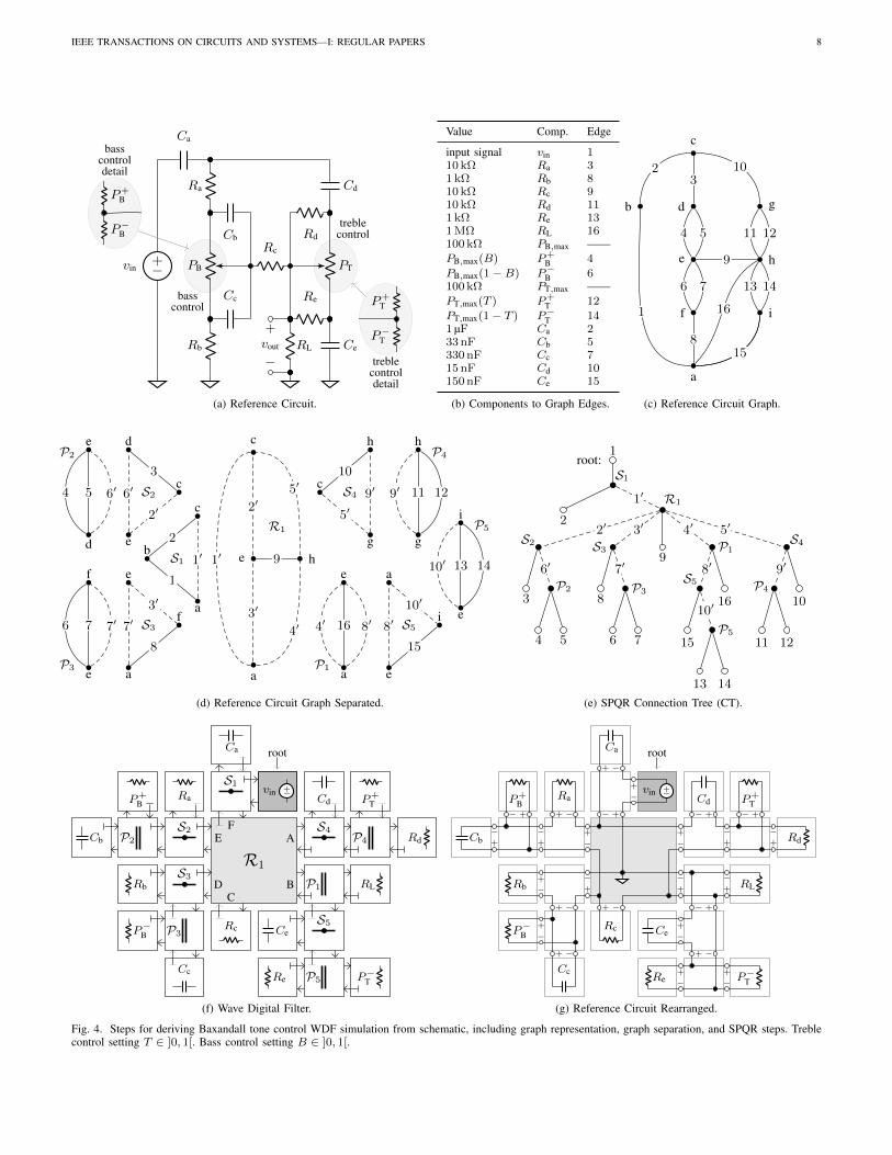
IEEE TRANSACTIONS ON CIRCUITS AND SYSTEMS—I: REGULAR PAPERS 8
basscontrol
treblecontrol
−+vin
Ca
Cd
PT
Ce
Ra
PB
Rb
Cc
Cb
Re
RdRc
RL
+vout
−
basscontroldetail
treblecontroldetail
P+B
P−B
P+T
P−T
(a) Reference Circuit.
Value Comp. Edge
input signal vin 110 kΩ Ra 31 kΩ Rb 810 kΩ Rc 910 kΩ Rd 111 kΩ Re 131 MΩ RL 16100 kΩ PB,max ——PB,max(B) P+
B 4
PB,max(1−B) P−B 6
100 kΩ PT,max ——PT,max(T ) P+
T 12
PT,max(1− T ) P−T 14
1 µF Ca 233 nF Cb 5330 nF Cc 715 nF Cd 10150 nF Ce 15
(b) Components to Graph Edges.
a
b
c
d
e
f
g
h
i1
8
16
15
23
10
4 5
6 7
9
11 12
13 14
15
(c) Reference Circuit Graph.
a
c
e h9
R1
1′
2′
3′
4′
5′
b
c
a
S1
1
1′2
c
d
e
S2
2′6′
3
f
e
a
S3
8
7′3′
c
h
g
S4
5′9′
10
i
a
e
S5
15
8′10′
e
aP1
4′ 16 8′
e
d
P2
4 5 6′
f
eP3
6 7 7′
h
g
P4
9′ 11 12
i
e
P5
10′ 13 14
(d) Reference Circuit Graph Separated.
6′
2′
7′
3′
10′
8′
4′
9′
5′
1′
1
2
3
4 5 6 7
8
9
10
11 12
13 14
15
16
S1
S2 S3S4
S5
P1
P2 P3 P4
P5
R1
root:
(e) SPQR Connection Tree (CT).
Ca
−+vin
Rd
CdRa
Cb
Rc
Rb
Cc
P+B
P−B
P+T
RL
P−TRe
Ce
root
R1
S1
S2
S3
S4
S5
P1
P2
P3
P4
P5
A
BC
D
EF
(f) Wave Digital Filter.
Ca
−+vin
Rd
CdRa
Cb
Rc
RLRb
Cc
P+B
P−B
P+T
Ce
Re P−T
−+
+
−
+
−
−+
−+
+
−
+
−
+
−
+
−
−+
+
−
+
−
−+
−+
−+
+ − + −
+ − + − − +
− + + − − + − + − +
+ −root
(g) Reference Circuit Rearranged.
Fig. 4. Steps for deriving Baxandall tone control WDF simulation from schematic, including graph representation, graph separation, and SPQR steps. Treblecontrol setting T ∈ ]0, 1[. Bass control setting B ∈ ]0, 1[.

IEEE TRANSACTIONS ON CIRCUITS AND SYSTEMS—I: REGULAR PAPERS 9
Frequency (Hz)
Mag
nit
ud
e (V
/dB
)P
has
e (r
adia
ns)
(a) Varying bass control B.
Frequency (Hz)
(b) Varying treble control T .
Fig. 5. Magnitude |H| and phase ∠H responses of Baxandall tone control.
TABLE IVQUANTITIES, CASE STUDY R-TYPE ADAPTOR IMPLEMENTATIONS
Number of variable Baxandall tone Frequency Booster
Ports N 6 8(Non-datum) nodes n 3 5Extra MNA variables m 0 1
Figs. 5a–5b show frequency responses H = Vout/Vin forvarious bass control settings B ∈ ]0, 1[ (treble control fixedat T = 0.1) and various treble control settings T ∈ ]0, 1[(bass control fixed at B = 0.1). The WDF model’s frequencyresponses are found by taking the Discrete Fourier Transformof measured unit-amplitude impulse responses. Dashed linesshowing the analog response calculated using SPICE [21]and solid lines showing the WDF response have excellentagreement. The only visible distortions are the expected high-frequency warping from the bilinear transform [50]. TheBaxandall tone control has weakly parametric controls. For in-stance, the bass control B primarily affects a bass “shelf” levelbut also affects the cutoff frequency, ripple in the transitionband, shape of the shelf corners, etc. Control parametrizationis an important part of VA [51]; by modeling the circuitusing WDFs we obtain this parametrization as a byproductof properly modeling the reference circuit’s dynamics.
Relevant quantities for analyzing R1’s implementation costin multiplies are shown in Tab. IV. The costs of (24)–(27)(from Tab. III) are shown for various wave types and comparedagainst nominal scattering matrix multiplication (20)–(23)and the method of Martens and Meerkotter [27] in Tab. V.The minimum implementation cost for each wave type isdarkly highlighted and bolded, and any implementation thatis cheaper than the nominal is lightly highlighted. For ρ 6= 1,using (27) (Nor.+Vol.) minimizes the number of multiplies,reducing the cost compared to the nominal by about 58.3% or41.7%, depending on the wave type. For voltage waves (ρ =1), Martens and Meerkotter has the lowest implementationcost. This is the case in general for voltage-wave simulationsof passive reciprocal circuits. However, while the method ofMartens and Meerkotter cannot be used at all for other wavetypes, our proposed approach suffers no such restrictions.
TABLE VNO. OF MULTIPLIES, CASE STUDY R-TYPE ADAPTOR IMPLEMENTATIONS
Baxandall tone Frequency Booster
basis ρ = ρ =
eq. sol. equiv. 1 0 else 1 0 else hybrid
(24) Cur. The. 42 42 48 72 72 80 79(25) Cur. Nor. 30 18 30 56 40 56 54(26) Vol. The. 18 30 30 40 56 56 56(27) Vol. Nor. 15 15 21 33 33 41 40
(20)–(23) nominal S 36 36 36 64 64 64 64
Martens & Meerkotter 9 —– —– —– —– —– —–
B. Frequency Booster Pedal
The schematic of an op-amp based “Frequency Booster”guitar pedal circuit is shown in Fig. 6a. It is based on adesign by Anderton [52] (possibly via Hutchins [53], [54])with additional biasing circuitry [54]. This circuit allows theuser to add a parametric boost around one of five centerfrequencies. The circuit is essentially a type-16 Sallen–Keyfilter [55] with an extra dc coupling capacitor (Cz), extrabiasing (R0, Ra, Rd, Ca, and Vb), and an extra high pass (Rgand Cd) on the output. The amplifier (op-amp, Re, Rf, andCc) is not frequency-independent as in the traditional Sallen–Key design, but has a first-order high pass cutoff around 3 Hz.The input is an ideal voltage source vin and the output is thevoltage across Rg. The circuit comprises 5 capacitors (Cz andCa · · ·Ce), 7 resistors (R0, Ra, and Rc · · ·Rh), a potentiometer(Rb) controlling the boost amount, an op-amp, and a battery(dc ideal voltage source Vb). The op-amp is configured innegative feedback and modeled as ideal using a nullor [33].
1) WDF Model: A graph representing the circuit is shownin Fig. 6c. Circuit nodes correspond to graph nodes a · · · kand electrical components correspond to graph edges 1 · · · 16;component values and mappings to graph edges are given inFig. 6b. The unlabeled gray graph edges connected to nodes a,f, g, j are a replacement graph representing the op-amp (nullor)and keep this two-port contained inside a single junction (thesame technique used for transformers in [26]). Using the graphseparation algorithm of [26] yields a decomposition (Fig. 6d)into 5 series (S1 · · · S5), 3 parallel (P1 · · · P3), and 1 rigidconnection (R1). Designating vin (edge 1) as the root, thegraph decomposition yields an SPQR tree (Fig. 6e) isomorphicto a WDF adaptor structure (Fig. 6f) retaining the topologyof the reference circuit (Fig. 6g). The series/parallel adaptorsand one-ports of Fig. 6f are implemented using classical WDFtechniques. The scattering behavior of R1 is derived using theproposed technique of this article and shown here in depth.R1 involves an absorbed nullor and has six nodes 0 – 5
(Fig. 7a). Port voltages and currents for the 8 ports A · · ·Hare labeled. Thevenin (Fig. 7b) or Norton (Fig. 7c) equiva-lents represent the incident waves aA · · · aH. Using Theveninequivalents, eight additional nodes 6 – 13 are added to thecircuit. Using Norton Type 1 equivalents, the same is true butthe extra nodes define shorts with currents jA · · · jH. UsingNorton Type 2 equivalents, these shorts are omitted.
Matrices X0, X1, and Ap (Tab. VI) are formed by using

IEEE TRANSACTIONS ON CIRCUITS AND SYSTEMS—I: REGULAR PAPERS 10
op-amp
−
+
nullormodel ofop-amp
−
+
Vb
R0
CaRa
Rd
Cz
−+vin
Cb Ce
Rh
Cc Re Rf
Cd
Rg
RbRc
+vout
−
v+
v−
(a) Reference Circuit.
Value Comp. Edge
input signal vin 1100 kΩ Ra 410 kΩ Rb,max ——Rb,max (Q) Rb 135.6 kΩ Rc 141 MΩ Rd 610 kΩ Re 1110 kΩ Rf 12100 kΩ Rg 1610 kΩ Rh 79 V, 100 kΩ Vb, R0 32.2 µF Cz 210 µF Ca 5(C) Cb 810 µF Cc 102.2 µF Cd 15(C) Ce 9
(b) Graph Edges.
a
b
cd
e
f
g
h
i
j
k
4 53
6
2 8 9
7
15
13
16
1
10
11
14
12
(c) Reference Circuit Graph.
a
ce
f
g
j
a
jj
h
e
k
a
i
g
a
d
c
a
c
a
ba
b
a
c
b4′
8 9
7
2′
3′
1′
12
2′
1′
15
16
14
13
3′10
11
5′1
2
7′6′
6
5′ 4′6′5 7′8′
4 8′3 S2 S3
S1 S4
S5
P3P2
P1
R1
(d) Reference Circuit Graph Separated.
8′
7′
6′
3′ 2′ 1′
4′
5′
1
2
3 4
5
6 7 8 9
10 11
12
13 1415 16
S1
S2
S3 S4 S5
P1
P2
P3
R1
root:
(e) SPQR Connection Tree (CT).− +
vin
Cz
Ca
Ra
Rb
Rc
Cb
Rd
Cc
Re
Rf
Cd
Rg
Ce
Rh R1
P1
P2 P3
S1
S2 S3
S4
S5
A
BC D
E
FG
H
VbR0
root
(f) Wave Digital Filter.
− +
vin
Cz
Ca
Ra
Rb
Rc
Cb
Rd
Cc
Re
Rf
Cd
Rg
Ce
Rh
−+
−+
+
−−+
+
−
+
−
+
−−+
+
−
+
−+
−+
−
+ −
− ++ −
+ −
+ − − + + −
+ −− + − +
+ −
− +
VbR0
root
v+v−
(g) Reference Circuit Rearranged.
Fig. 6. Steps for deriving Frequency Booster WDF simulation from schematic, including graph representation, graph separation, and SPQR steps. Qualityfactor “Q” control setting Q ∈ ]0, 1]. Capacitor pair value C ∈ 0.22, 0.1, 0.02, 0.01, 0.005 µF.

IEEE TRANSACTIONS ON CIRCUITS AND SYSTEMS—I: REGULAR PAPERS 11
iH
iA
iB
iE
iF
iC iD
iG
−
+
−
+
+
−
+
−
−
+
− + − +
+ −
vH
vA
vB vE
vF
vC vD
vG
0
1
2
3
4
5
(a) R1 port definitions.
−+
−+
−+
−+
−+
− + − +
−+
gH
gA
gB
gE
gF
gC gD
gG
RH
RA
RB
RE
RF
RC
RD
RG
jH
jA
jB
jE
jF
jC jD
jG
iH
iA
iB
iE
iF
iC iD
iG
−
+
−
+
+
−
+
−
−
+
− + − +
+ −
vH
vA
vB vE
vF
vC vD
vG
0
1
2
3
4
5
13
6
7
8 9
10
11
12
gx = R1−ρx ax
(b) R1 + Thevenin equivalents.
RH
RA
RB
RE
RF
RC RD
RG
gH
gA
gB
gE
gF
gC gD
gG
jH
jA
jB
jE
jF
jC jD
jG
iH
iA
iB
iE
iF
iC iD
iG
−
+
−
+
+
−
+
−
−
+
− + − +
+ −
vH
vA
vB vE
vF
vC vD
vG
0
1
2
3
4
5
13
6
7
8 9
10
11
12
gx = R−ρx ax
(c) R1 + Norton equivalents.
Fig. 7. R-type junction definition for Frequency Booster and two versions of instantaneous port equivalents.
the Thevenin and Norton equivalent stamps from Tab. II andthe nullor stamp from Tab. I. As an example, the stampscorresponding to port A are highlighted in light gray and thestamps corresponding to the nullor are highlighted in darkgray. Although we have chosen to model the op-amp witha nullor, consider modeling it with a VCVS as a thoughtexperiment [33]. The procedure would be identical althoughthe VCVS stamp from Tab. I would replace the nullor stamp.
In forming X0 or X1 and Ap from X0 or X1 and Ap, any“internal” node 0 – 5 may be selected as the datum node aslong as it is removed consistently from all matrices. As withother WDF adaptors, the upwards-facing port resistance RH ischosen to adapt port H (i.e., to set SHH = 0). This is done by
RH =RB(RARD −RCRG)− (RA +RB +RC)RERG
(RA +RB +RC)RD.
2) Discussion: The model’s frequency response H =Vout/Vin is characterized for a variety of boost and centerfrequency settings in Fig. 8, where nominal center frequencies(Cb and Ce values) for each setting are shown with verticallines. Rb cannot go to zero, i.e., Q ∈ ]0, 1]. For the curves inFig. 8, there is excellent agreement between the analog andWDF responses. The only visible error is high frequency bilin-ear transform warping. The boost control is weakly parametric;increasing the boost also alters the center frequency.
Since the Frequency Booster is an active circuit, it ispossible that adaptation requires negative port resistances.Indeed, given the circuit values in Fig. 6b, that is the casefor the upward-facing ports of R1, P3, and S2: the threeadaptors between the nullor and the root of the tree (vin). If thesame wave definition is used in the entire WDF structure, thepresence of negative port resistances would disallow the use ofany wave type except voltage and current waves. An exampleof two strategies for localizing this restriction are shown inFig. 9. On account of the negative port resistances, P3, S2,
Cz, and vin all use voltage waves (ρ = 1). To interface thisto a power waves (ρ = 1/2) part of the simulation, a waveconverter is used between S1 and P3. R1 is treated using the“hybrid-wave junction” technique so that most of its ports canuse power waves. Ports A · · ·G use power waves and port Huses voltage waves; R1 is parametrized by the vector
ρ = [ ρA, · · · , ρG, ρH ]> = [ 1/2, · · · , 1/2, 1 ]> . (32)
In this way, the majority of the adaptors and one-ports in theWDF structure, including most of R1, can use power-wavesdespite the presence of negative port resistances.
Relevant quantities for analyzing R1’s implementation costin multiplies are shown in Tab. IV. The cost (from Tab. III)of (24)–(27) are shown for various wave types and comparedagainst the nominal scattering matrix multiplication (20)–(23) in Tab. V. The column “ρ = else” is shown only togive a more complete sense of the computational impact ofthe wave parametrization; the negative port restrictions placesome restrictions on wave definitions. The hybrid parametriza-tion (32) can be used when power waves are preferred. Theuse of (27) (Nor.+Vol.) minimizes the number of multipliesneeded, reducing the cost compared to the nominal scatteringmatrix multiplication by about 48.4% if voltage or currentwaves are used or 37.5% if (32) is used.
V. CONCLUSION
In this article, we expanded the class of circuits that canbe modeled using the Wave Digital Filter approach to includeactive and non-reciprocal circuits. Beyond accomodating all ofthe topological ways that linear two-ports can be embeddedin a circuit, this enables WDF modeling of circuits involvingthe important nullor element. Since the two-port scatteringbehavior of the nullor is undefined [22], they would previouslyhave been intractable in a WDF simulation.

IEEE TRANSACTIONS ON CIRCUITS AND SYSTEMS—I: REGULAR PAPERS 12
TABLE VIFREQUENCY BOOSTER R-TYPE ADAPTOR MATRICES X0 , X1 , AND AP WITH CORRRESPONDING CASES LABELLED.
MNA system matrix X1, for Vol.+The., Cur.+The., or Cur.+Nor. (Type 1) cases
GF +GH 0 0 0 0 0 0 0 0 0 0 −GF 0 −GH 0 0 0 0 0 0 −1 0 −10 GA 0 0 0 0 −GA 0 0 0 0 0 0 0 0 −1 0 0 0 0 0 −1 00 0 GB 0 0 0 0 −GB 0 0 0 0 0 0 0 0 −1 0 −1 0 0 0 00 0 0 GC 0 0 0 0 −GC 0 0 0 0 0 −1 0 0 0 0 0 0 0 00 0 0 0 GG 0 0 0 0 0 0 0 −GG 0 0 0 0 −1 0 0 0 0 00 0 0 0 0 GD +GE 0 0 0 −GD −GE 0 0 0 0 0 0 0 0 −1 0 0 +10 −GA 0 0 0 0 GA 0 0 0 0 0 0 0 +1 0 0 0 0 0 0 0 00 0 −GB 0 0 0 0 GB 0 0 0 0 0 0 0 +1 0 0 0 0 0 0 00 0 0 −GC 0 0 0 0 GC 0 0 0 0 0 0 0 +1 0 0 0 0 0 00 0 0 0 0 −GD 0 0 0 GD 0 0 0 0 0 0 0 +1 0 0 0 0 00 0 0 0 0 −GE 0 0 0 0 GE 0 0 0 0 0 0 0 +1 0 0 0 0
−GF 0 0 0 0 0 0 0 0 0 0 GF 0 0 0 0 0 0 0 +1 0 0 00 0 0 0 −GG 0 0 0 0 0 0 0 GG 0 0 0 0 0 0 0 +1 0 0
−GH 0 0 0 0 0 0 0 0 0 0 0 0 GH 0 0 0 0 0 0 0 +1 00 0 0 −1 0 0 +1 0 0 0 0 0 0 0 0 0 0 0 0 0 0 0 00 −1 0 0 0 0 0 +1 0 0 0 0 0 0 0 0 0 0 0 0 0 0 00 0 −1 0 0 0 0 0 +1 0 0 0 0 0 0 0 0 0 0 0 0 0 00 0 0 0 −1 0 0 0 0 +1 0 0 0 0 0 0 0 0 0 0 0 0 00 0 −1 0 0 0 0 0 0 0 +1 0 0 0 0 0 0 0 0 0 0 0 00 0 0 0 0 −1 0 0 0 0 0 +1 0 0 0 0 0 0 0 0 0 0 0
−1 0 0 0 0 0 0 0 0 0 0 0 +1 0 0 0 0 0 0 0 0 0 00 −1 0 0 0 0 0 0 0 0 0 0 0 +1 0 0 0 0 0 0 0 0 00 0 0 +1 −1 0 0 0 0 0 0 0 0 0 0 0 0 0 0 0 0 0 0
0 1 2 3 4 5 6 7 8 9 10 11 12 13 A B C D E F G H inor
internal node voltages, vn,1 port-related ( β stamp) node voltages, vn,2 Thevenin source or short currents, jb,1 jb,2
012345678910
1112
13ABCDEFGH
vnull
KC
L,i
nt.n
odes
KC
L,p
ort
node
sT
he.s
ourc
e/
shor
tde
f.
MNA system matrix X0, for Vol.+Nor. (Type 2) case port incidence matrix, Ap
GF +GH +G −GH 0 0 −GG −GF −1−GH GA +GB +GH −GB −GA 0 0 0
0 −GB GB +GC +GE −GC 0 −GE 00 −GA −GC GA +GC 0 0 0
−GG 0 0 0 GD +GG −GD 0−GF 0 −GE 0 −GD GD +GE +GF +1
0 0 0 +1 −1 0 0
0 1 2 3 4 5 inor
internal node voltages, vn,1 jb,2
0123
45
vnull
KC
L,i
nt.n
odes
0 0 0 0 0 +1 −1 +1+1 −1 0 0 0 0 0 −1
0 +1 −1 0 −1 0 0 0−1 0 +1 0 0 0 0 0
0 0 0 −1 0 0 +1 00 0 0 +1 +1 −1 0 0
A B C D E F G H
ports
0
12
345in
tern
alno
des
Ph
ase
(rad
ian
s)
Frequency (Hz)
Mag
nit
ud
e (V
/dB
)
Fig. 8. Magnitude |H| and phase ∠H responses of Frequency Booster pedal.
First, a known technique [26] was shown to yield WDFstructures involving R-type adaptors for circuits with ac-tive linear elements. Second, four parametric-wave scatteringequations were developed for the unbounded class of R-typejunctions. Third, three of these equations were shown to haveimplementation costs in multiplies that are usually cheaperthan the cost of an N × N matrix multiply, with one (27)usually being the cheapest. Finally, wave converter two-portsand hybrid-wave junctions were introduced to enable multiple
wave types to coexist, localizing restrictions on wave type.The proposed methods do not introduce any loss of accuracy
using infinite precision arithmetic. Although we have notexperienced any numerical issues in practice, the proposedmethods for R-type adaptor scattering do not enjoy the sameguarantee of pseudo-passivity as the classical basic WDFadaptors [1], [8]. Future work could investigate this detail.
The findings of this article have implications for WDFmodeling of nonlinear circuits, which is a major topic [2],[12], [14], [17], [18], [43], [56]–[67]. In [68], Werner et al.showed one approach that groups all nonlinearities at theroot of a tree and interfaces them to the rest of the circuitusing an R-type adaptor. The local implicit relationship thatis created is resolved using, e.g., table lookup [68] or Newton–Raphson iteration [69]. This in theory enables systematic WDFsimulation of circuits with any number of nonlinearities whichwere previously out of scope for WDF modeling, includingthe Electro-Harmonix Big Muff Pi [68], transistor [69] andtriode [70] amplifiers, the Fender 5F6-A preamplifier [71], theKorg MS-50 VCF [72], relaxation oscillators [20], previouslyintractable types of diode clippers [73], and the Bass Drumcircuit from the Roland TR-808 [39]. It also admits extensionsfor circuits with certain topological properties [73]. Futurework should focus on incorporating the findings of this articleinto simulations of active, nonlinear circuits.

IEEE TRANSACTIONS ON CIRCUITS AND SYSTEMS—I: REGULAR PAPERS 13
11/211/2
− +
vin
Cz
Ca
Ra
Rb
Rc
Cb
Rd
Cc
Re
Rf
Cd
Rg
Ce
Rh
R1
hybrid-waveadaptor
P1
P2 P3
S1
S2 S3
S4
S5
waveconverter
A
BC D
E
FG
H
VbR0
root
voltage waves
power waves
multiple waves
Fig. 9. Freq. Booster WDF with hybrid-wave adaptor and wave converter.
REFERENCES
[1] A. Fettweis, “Wave digital filters: Theory and practice,” Proc. IEEE,vol. 74, no. 2, pp. 270–327, Feb. 1986.
[2] G. De Sanctis and A. Sarti, “Virtual analog modeling in the wave-digitaldomain,” IEEE Trans. Audio, Speech, Language Process., vol. 18, no. 4,pp. 715–727, May 2010.
[3] J. O. Smith, Physical Audio Signal Processing. W3K Publishing, 2010.[4] A. Fettweis, “Some principles of designing digital filters imitating
classical filter structures,” IEEE Trans. Circuit Theory, vol. 18, no. 2,pp. 314–316, Mar. 1971.
[5] ——, “Digital filters structures related to classical filter networks,” Arch.Elek. Ubertragung., vol. 25, pp. 79–89, Feb. 1971.
[6] V. Belevitch, Classical Network Theory. San Francisco, CA: Holden-Day, 1968.
[7] A. Fettweis and K. Meerkotter, “On adaptors for wave digital filters,”IEEE Trans. Acoust., Speech, Signal Process., vol. 23, no. 6, pp. 516–525, Dec. 1975.
[8] A. Fettweis, “Pseudo-passivity, sensitivity, and stability of wave digitalfilters,” IEEE Trans. Circuit Theory, vol. 19, no. 6, pp. 668–673, Nov.1972.
[9] A. Sedlmeyer and A. Fettweis, “Digital filter with true ladder configu-ration,” Circuit Theory Appl., vol. 1, pp. 5–10, 1973.
[10] A. Fettweis, H. Levin, and A. Sedlmeyer, “Wave digital lattice filters,”Circuit Theory Appl., vol. 2, pp. 203–211, 1974.
[11] J. O. Smith III, “Waveguide filter tutorial,” in Proc. Int. Comput. MusicConf., Champaign-Urbana, IL, Aug. 1987, pp. 9–16.
[12] A. Sarti and G. De Poli, “Toward nonlinear wave digital filters,” IEEETrans. Signal Process., vol. 47, no. 6, pp. 1654–1668, June 1999.
[13] F. Pedersini, A. Sarti, and S. Tubaro, “Object-based sound synthesisfor virtual environments using musical acoustics,” IEEE Signal Process.Mag., vol. 17, no. 6, pp. 37–51, Nov. 2000.
[14] A. Sarti and G. De Sanctis, “Systematic methods for the implementationof nonlinear wave-digital structures,” IEEE Trans. Circuits Syst. I, Reg.Papers, vol. 56, no. 2, pp. 460–472, Feb. 2009.
[15] A. Fettweis and G. Nitsche, “Numerical integration of partial differentialequations by means of multidimensional wave digital filters,” in Proc.IEEE Int. Symp. Circuits Syst., New Orleans, LA, May 1990, pp. 954–957.
[16] S. Bilbao, Wave and Scattering Methods for Numerical Simulation. NewYork, NY: Wiley, 2004.
[17] M. Karjalainen and J. Pakarinen, “Wave digital simulation of a vacuum-tube amplifier,” in IEEE Int. Conf. Acoust., Speech, Signal Process.,Toulouse, France, May 2006, pp. 153–156.
[18] D. T.-M. Yeh, “Digital implementation of musical distortion circuits byanalysis and simulation,” Ph.D. diss., Stanford Univ., CA, June 2009.
[19] D. Franken and K. Ochs, “Automatic step-size control in wave digitalsimulation using passive numerical integration methods,” Int. J. Electron.Commun., vol. 58, pp. 391–401, 2004.
[20] M. J. Olsen, K. J. Werner, and F. G. Germain, “Network variablepreserving step-size control in wave digital filters,” in Proc. 20th Int.Conf. Digital Audio Effects, Edinburgh, UK, Sept. 2017, pp. 200–207.
[21] A. Vladimirescu, The SPICE Book. New York, NY: Wiley, 1994.
[22] H. J. Carlin, “Singular network elements,” IEEE Trans. Circuit Theory,vol. 11, no. 1, pp. 67–72, Mar. 1964.
[23] L. T. Bruton, RC-Active Circuits: Theory and Design. EnglewoodCliffs, NJ: Prentice-Hall, 1980.
[24] M. Karjalainen, “Efficient realization of wave digital components forphysical modeling and sound synthesis,” IEEE Trans. Audio, Speech,Language Process., vol. 16, no. 5, pp. 947–956, July 2008.
[25] K. J. Werner, J. O. Smith III, and J. S. Abel, “Wave digital filter adaptorsfor arbitrary topologies and multiport linear elements,” in Proc. 18th Int.Conf. Digital Audio Effects, Trondheim, Norway, Nov. 2015, pp. 379–386.
[26] D. Franken, J. Ochs, and K. Ochs, “Generation of wave digital structuresfor networks containing multiport elements,” IEEE Trans. Circuits Syst.I, Reg. Papers, vol. 52, no. 3, pp. 586–596, Mar. 2005.
[27] G. O. Martens and K. Meerkotter, “On N-port adaptors for wave digitalfilters with application to a bridged-tee filter,” in Proc. IEEE Int. Symp.Circuits Syst., Munich, Germany, Apr. 1976, pp. 514–517.
[28] H. H. Le, “Wave digital adaptors for Brune, Darlington C and D, andtwin-T sections,” Ph.D. diss., Univ. Manitoba, Winnipeg, Canada, 1977.
[29] G. O. Martens and H. H. Le, “Wave digital adaptors for reciprocalsecond-order sections,” IEEE Trans. Circuits Syst., vol. 25, no. 12, pp.1077–1083, Dec. 1978.
[30] K. Meerkotter and D. Franken, “Digital realization of connection net-works by voltage-wave two-port adaptors,” Arch. Elek. Ubertragung.,vol. 50, no. 6, pp. 362–367, 1996.
[31] K. J. Werner, V. Nangia, J. O. Smith III, and J. S. Abel, “A generaland explicit formulation for wave digital filters with multiple/multiportnonlinearities and complicated topologies,” in Proc. IEEE Work. Appl.Signal Process. Audio Acoust., New Paltz, NY, Oct. 2015.
[32] C.-W. Ho, A. E. Ruehli, and P. A. Brennan, “The modified nodalapproach to network analysis,” IEEE Trans. Circuits Syst., vol. 22, no. 6,pp. 504–509, June 1975.
[33] K. J. Werner, W. R. Dunkel, M. Rest, M. J. Olsen, and J. O. Smith III,“Wave digital filter modeling of circuits with operational amplifiers,” inProc. Eur. Signal Process. Conf., Budapest, Hungary, Aug. 2016, pp.1033–1037.
[34] K. J. Werner, W. R. Dunkel, and F. G. Germain, “A computational modelof the Hammond organ vibrato/chorus using wave digital filters,” inProc. 19th Int. Conf. Digital Audio Effects, Brno, Czech Republic, Sept.2016, pp. 271–278.
[35] F. G. Germain and K. J. Werner, “Optimizing differentiated discretizationfor audio circuits beyond driving point transfer functions,” in Proc. IEEEWork. Appl. Signal Process. Audio Acoust., New Paltz, NY, Oct. 2017.
[36] O. Bogason, “Digitizing analog circuits containing op amps using wavedigital filters,” Online Blog, URL: http://obogason.com/emulating-op-amp-circuits-using-wdf-theory/, Mar. 20 2016.
[37] M. Verasani, A. Bernardini, and A. Sarti, “Modeling Sallen-Key audiofilters in the wave digital domain,” in Proc. IEEE Int. Conf. Acoust.,Speech Signal Process., New Orleans, LA, Mar. 2017, pp. 431–435.
[38] O. Bogason and K. J. Werner, “Modeling circuits with operationaltransconductance amplifiers using wave digital filters,” in Proc. 20th Int.Conf. Digital Audio Effects, Edinburgh, UK, Sept. 2017, pp. 130–137.
[39] K. J. Werner, “Virtual analog modeling of audio circuitry using wavedigital filters,” Ph.D. diss., Stanford Univ., CA, Dec. 2016.
[40] G. Kubin, “Wave digital filters: Voltage, current, or power waves?” inIEEE Int. Conf. Acoust., Speech, Signal Process., Tampa, FL, Apr. 1985,pp. 69–72.
[41] S. D’Angelo and V. Valimaki, “Wave-digital polarity and current invert-ers and their application to virtual analog audio processing,” in IEEEInt. Conf. Acoust., Speech Signal Process., Kyoto, Japan, Mar. 2012.
[42] J. Vlach and K. Singhal, Computer Methods for Circuit Analysis andDesign. New York, NY: Van Nostrand Reinhold Company, 1983.
[43] A. Bernardini, P. Maffezzoni, L. Daniel, and A. Sarti, “Wave-basedanalysis of large nonlinear photovoltaic arrays,” IEEE Trans. CircuitsSyst. I, Reg. Papers, vol. 65, no. 4, pp. 1363–1376, Apr. 2018.
[44] I. M. Gottlieb, Practical Oscillator Handbook. Oxford, UK: Newnes,1997.
[45] P. J. Baxandall, “Negative-feedback tone control,” Wireless World, pp.402–405, Oct. 1952.
[46] V. Valimaki and J. D. Reiss, “All about audio equalization: Solutionsand frontiers,” Appl. Sci., vol. 6, no. 5, 2016, article #129.
[47] D. Self, Small Signal Audio Design. Oxford, UK: Focal Press, 2010.[48] V. Valimaki, S. Bilbao, J. O. Smith III, J. S. Abel, J. Pakarinen, and
D. Berners, “Virtual analog effects,” in DAFx: Digital Audio Effects,2nd ed., U. Zolzer, Ed. West Sussex, UK: Wiley, 2011, ch. 12, pp.473–522.

IEEE TRANSACTIONS ON CIRCUITS AND SYSTEMS—I: REGULAR PAPERS 14
[49] M. Giles, Ed., Audio/Radio Handbook. Santa Clara, CA: NationalSemiconductor Corp., 1980.
[50] F. G. Germain and K. J. Werner, “Design principles for lumped modeldiscretisation using Mobius transforms,” in Proc. 18th Int. Conf. DigitalAudio Effects, Trondheim, Norway, Nov. 2015, pp. 371–378.
[51] D. T.-M. Yeh and J. O. Smith III, “Discretization of the ’59 FenderBassman tone stack,” in Proc. 9th Int. Conf. Digital Audio Effects,Montreal, Canada, Sept. 2006, pp. 1–5.
[52] C. Anderton, Projects for Guitarists. San Francisco, CA: MillerFreeman Books, 1995, Project 10: The Frequency Booster.
[53] B. Hutchins, “A simple mid-range booster,” Electronotes ApplicationNotes, vol. AN-215, May 1981.
[54] J. Orman, “Anderton frequency booster,” Online Blog, URL:http://www.muzique.com/news/frequency-booster/, Nov. 2010.
[55] R. P. Sallen and E. L. Key, “A practical method of designing RC activefilters,” IRE Trans. Circuit Theory, vol. 2, no. 1, pp. 74–85, Mar. 1955.
[56] K. Meerkotter and R. Scholz, “Digital simulation of nonlinear circuits bywave digital filter principles,” in IEEE Int. Symp. Circuits Syst., Portland,OR, May 1989, pp. 720–723.
[57] S. Petrausch and R. Rabenstein, “Wave digital filters with multiplenonlinearities,” in Proc. Eur. Signal Process. Conf., Vienna, Austria,Sept. 2004, pp. 77–80.
[58] R. C. D. Paiva, S. D’Angelo, J. Pakarinen, and V. Valimaki, “Emulationof operational amplifiers and diodes in audio distortion circuits,” IEEETrans. Circuits Syst. II, Exp. Briefs, vol. 59, no. 10, pp. 688–692, Oct.2012.
[59] K. J. Werner, V. Nangia, A. Bernardini, J. O. Smith III, and A. Sarti, “Animproved and generalized diode clipper model for wave digital filters,”in Proc. 139th Conv. Audio Eng. Soc., New York, NY, Oct. 2015, conv.paper. #9360.
[60] T. Schwerdtfeger and A. Kummert, “A multidimensional approach towave digital filters with multiple nonlinearities,” in Proc. Eur. SignalProcess. Conf., Lisbon, Portugal, Sept. 2014, pp. 2405–2409.
[61] ——, “Newton’s method for modularity-preserving multidimensionalwave digital filters,” in Proc. IEEE Int. Work. Multidimensional Syst.,Vila Real, Portugal, Sept. 2015.
[62] A. Bernardini, K. J. Werner, A. Sarti, and J. O. Smith III, “Modelingnonlinear wave digital elements using the Lambert function,” IEEETrans. Circuits Syst. I, Reg. Papers, vol. 63, no. 8, pp. 1231–1242, Aug.2016.
[63] O. B. Bogason, “Modeling audio circuits containing typical nonlinearcomponents with wave digital filters,” Master’s thesis, McGill Univ.,Montreal, Canada, Apr. 2018.
[64] A. Bernardini and A. Sarti, “Biparametric wave digital filters,” IEEETrans. Circuits Syst. I, Reg. Papers, vol. 64, no. 7, pp. 1826–1838, July2017.
[65] ——, “Dynamic adaptation of instantaneous nonlinear bipoles in wavedigital networks,” in Proc. Eur. Signal Process. Conf., Budapest, Hun-gary, Aug. 2016, pp. 1038–1042.
[66] ——, “Canonical piecewise-linear representation of curves in the wavedigital domain,” in Proc. Eur. Signal Process. Conf., Kos, Greece, Aug.2017, pp. 1125–1129.
[67] A. Bernardini, K. J. Werner, P. Maffezzoni, , and A. Sarti, “Wave digitalmodeling of the diode-based ring modulator,” in Proc. 144nd Conv.Audio Eng. Soc., Milan, Italy, May 2018, conv. paper #10015.
[68] K. J. Werner, V. Nangia, J. O. Smith III, and J. S. Abel, “Resolvingwave digital filters with multiple/multiport nonlinearities,” in Proc. 18thInt. Conf. Digital Audio Effects, Trondheim, Norway, Nov. 2015, pp.387–394.
[69] M. J. Olsen, K. J. Werner, and J. O. Smith III, “Resolving groupednonlinearities in wave digital filters using iterative techniques,” in Proc.19th Int. Conf. Digital Audio Effects, Brno, Czech Republic, Sept. 2016,pp. 279–286.
[70] M. Rest, W. R. Dunkel, K. J. Werner, and J. O. Smith III, “RT-WDF—amodular wave digital filter library with support for arbitrary topologiesand multiple nonlinearities,” in Proc. 19th Int. Conf. Digital AudioEffects, Brno, Czech Republic, Sept. 2016, pp. 287–294.
[71] W. R. Dunkel, M. Rest, K. J. Werner, M. J. Olsen, and J. O. Smith III,“The Fender Bassman 5F6-A family of preamplifier circuits—a wavedigital filter case study,” in Proc. 19th Int. Conf. Digital Audio Effects,Brno, Czech Republic, Sept. 2016, pp. 263–270.
[72] M. Rest, J. D. Parker, and K. J. Werner, “WDF modeling of a KorgMS-50 based non-linear diode bridge VCF,” in Proc. 20th Int. Conf.Digital Audio Effects, Edinburgh, UK, Sept. 2017, pp. 145–151.
[73] K. J. Werner, M. J. Olsen, M. Rest, and J. D. Parker, “Root variablechoice in grouped wave digital filters,” in Proc. 20th Int. Conf. DigitalAudio Effects, Edinburgh, UK, Sept. 2017, pp. 176–183.
Kurt James Werner (S’14–M’17) received hisB.S. (2011) in General Engineering (with a sec-ondary field in Acoustics) and B.Music in The-ory and Composition, both from the University ofIllinois at Urbana-Champaign (UIUC). He earneda Ph.D. (2017) in Computer-Based Music Theoryand Acoustics from Stanford University’s Center forComputer Research in Music and Acoustics. He is aLecturer in Audio at the Sonic Arts Research Centre(SARC) of Queen’s University Belfast, where hejoined the faculty of Arts, Humanities and Social
Sciences and the School of Arts, English and Languages in 2017. His researchfocuses on theoretical aspects of wave digital filters, virtual analog modeling,computer modeling of circuit-bent instruments, sound synthesis, and thehistory of music technology. Dr. Werner is a member of the Audio EngineeringSociety (AES) and the International Computer Music Association (ICMA). Hehas been awarded best student paper awards from the IEEE WASPAA (2015)and (as second author) AES (2017). As co-author he was also awarded bestpaper no. 3 (DAFx, 2016) and a best paper honorable mention (DAFx, 2015).
Alberto Bernardini (S’16) received his B.S. fromthe University of Bologna, Italy, in 2012; and hisM.S. degree (cum laude) from the Politecnico diMilano, Italy, in 2015, both in Computer Engineer-ing. He is currently a Ph.D. candidate in Informa-tion Engineering at the Dipartimento di Elettronica,Informazione and Bioingegneria of the Politecnicodi Milano, Italy. His main research interests areaudio signal processing and modeling of nonlinearsystems.
Julius Orion Smith III (M’76) received theB.S.E.E. degree from Rice University, Houston, TX,in 1975 (control, circuits, and communication). Hereceived the M.S. and Ph.D. degrees in E.E. fromStanford University, Stanford, CA, in 1978 and1983, respectively. His Ph.D. research was devotedto improved methods for digital filter design andsystem identification applied to music and audiosystems. From 1975 to 1977, he worked in theSignal Processing Department at ESL, Sunnyvale,CA, on systems for digital communications. From
1982 to 1986, he was with the Adaptive Systems Department at SystemsControl Technology, Palo Alto, CA, where he worked in the areas of adaptivefiltering and spectral estimation. From 1986 to 1991, he was employed atNeXT Computer, Inc., responsible for sound, music, and signal processingsoftware for the NeXT computer workstation. After NeXT, he became anAssociate Professor at the Center for Computer Research in Music andAcoustics (CCRMA) at Stanford, teaching courses and pursuing researchrelated to signal processing techniques applied to music and audio systems.Continuing this work, he is presently Professor of Music and (by courtesy)Electrical Engineering at Stanford University. For more information, seehttp://ccrma.stanford.edu/∼jos/.
Augusto Sarti (M’04–SM’13) received his M.S. andhis Ph.D. in Electronics and Information Engineer-ing from the University of Padua, Italy, in 1988 and1993, respectively. In 1993, he joined the faculty ofthe Politecnico di Milano, Italy, where he is currentlya full professor. In 2013, he also joined the Uni-versity of California, Davis. His research interestsare in the area of multimedia signal processing,with particular focus on sound analysis, synthesisand processing; computational acoustics; and musicprocessing. He coauthored over 250 scientific publi-
cations on international journals and congresses as well as numerous patentsin the multimedia signal processing area. He coordinates the activities ofthe Musical Acoustics Lab and of the Sound and Music Computing Labof the Politecnico di Milano. He has been the promoter/coordinator and/orcontributor to numerous (20+) European projects. He is an active memberof the IEEE TC on Audio and Acoustics Signal Processing, and is in theEditorial Board of the IEEE.