modeling and simulation of variations in nano-cmos … · modeling and simulation of variations in...
TRANSCRIPT

Modeling and Simulation of Variations in Nano-CMOS Design
by
Yun Ye
A Dissertation Presented in Partial Fulfillment of the Requirements for the Degree
Doctor of Philosophy
Approved April 2011 by the Graduate Supervisory Committee:
Yu Cao, Chair Hongbin Yu
Hongjiang Song Lawrence Clark
ARIZONA STATE UNIVERSITY
May 2011

i
ABSTRACT
CMOS technology is expected to enter the 10nm regime for future integrated
circuits (IC). Such aggressive scaling leads to vastly increased variability, posing a
grand challenge to robust IC design. Variations in CMOS are often divided into two
types: intrinsic variations and process-induced variations. Intrinsic variations are
limited by fundamental physics. They are inherent to CMOS structure, considered as
one of the ultimate barriers to the continual scaling of CMOS devices. In this work
the three primary intrinsic variations sources are studied, including random dopant
fluctuation (RDF), line-edge roughness (LER) and oxide thickness fluctuation (OTF).
The research is focused on the modeling and simulation of those variations and their
scaling trends. Besides the three variations, a time dependent variation source,
Random Telegraph Noise (RTN) is also studied. Different from the other three
variations, RTN does not contribute much to the total variation amount, but
aggregate the worst case of Vth variations in CMOS. In this work a TCAD based
simulation study on RTN is presented, and a new SPICE based simulation method
for RTN is proposed for time domain circuit analysis. Process-induced variations
arise from the imperfection in silicon fabrication, and vary from foundries to
foundries. In this work the layout dependent Vth shift due to Rapid-Thermal
Annealing (RTA) are investigated. In this work, we develop joint thermal/TCAD
simulation and compact modeling tools to analyze performance variability under
various layout pattern densities and RTA conditions. Moreover, we propose a suite

ii
of compact models that bridge the underlying RTA process with device parameter
change for efficient design optimization.

iii
DEDICATION
This thesis is dedicated to my parents and my wife.

iv
ACKNOWLEDGMENTS
First and foremost I would like to thank my advisor, Professor Yu (Kevin) Cao. He
has been supportive since the days I began working in Nanoscale Integration and
MOdeling (NIMO) group. Ever since, Kevin has supported me not only by
providing a research assistantship with 30 days paid vacation per year, but also
academically and emotionally through the rough road to finish this thesis. Thanks to
him I had the opportunity to do researches on this topic, and to present my work to
other professions. He helped me come up with the thesis topic and guided me over
almost my whole Ph.D. study.
I am grateful to Dr. Hongbin Yu, Dr. Hongjiang Song, Dr. Lawrence Clark and Dr.
Chaitali Chaitali Chakrabarti for agreeing to be on my committee and for their time
and efforts in reviewing my work.
I would like to thank Dr. Sani Nassif and Dr. Frank Liu for their constructive
discussions and suggestions on this research work.
Dozens of people have helped and taught me immensely at the NIMO group.
Thanks Chi-Chao Wang for his valuable contribution to this work. We have three
papers collaborated with each other. Min Chen, Wei Zhao and Wenping Wang are
students before me, mentors in many ways. I would like to thank all other members
in NIMO: Jyothi Bhaskarr Velamala, Varsha Balakrishnan, Saurabh Sinha, Jia Ni, Rui
Zheng, Ketul Sutaria, and Venkatesa Ravi. You were a pleasure to work with.
Lastly, thank Student Recreation Complex.

v

vi
TABLE OF CONTENTS
Page
Chps. 1 INTRODUCTION ...................................................................................................... 1
Chps. 2 SIMULATION AND MODELING OF CMOS INTRINSIC
VARIATIONS ............................................................................................................... 6
2.1 Overview of Intrinsic Variations .......................................................................... 6
2.1.1 Random Dopant Fluctuation ........................................................... 6
2.1.2 Line Edge Roughness ....................................................................... 8
2.1.3 Oxide Thickness Fluctuations ....................................................... 10
2.1.4 Random Telegraph Noise .............................................................. 11
2.2 SPICE Based Statistical Simulation of Threshold Variation under Random
Dopant Fluctuation and Line-Edge Roughness. .................................................... 13
2.2.1 Introduction ..................................................................................... 13
2.2.2 Gate-Slicing Method ....................................................................... 16
2.2.3 Validation with Silicon Data .......................................................... 25
2.2.4 Interaction with Non-Rectangular Gate and Reverse Narrow
Width Effects .......................................................................................................... 28
2.2.5 Predictive Modeling of Threshold Variation ............................... 31
2.2.6 2-D Slicing Method for RDF ......................................................... 36
2.2.7 Summary ........................................................................................... 43

vii
2.3 Predictive Modeling of Fundamental CMOS Variations under Random
Geometry and Charge Fluctuations .......................................................................... 44
2.3.1 Introduction ..................................................................................... 44
2.3.2 Atomistic Simulation of Fundamental Variations ...................... 45
2.3.3. Predictive Modeling of Random Vth Variations ......................... 49
2.3.4 Minimization and Projection of Vth Variability ........................... 56
2.3.5 Summary ........................................................................................... 58
2.4 Simulation of Random Telegraph Noise with 2-Stage Equivalent Circuit . 58
2.4.1 Introduction ..................................................................................... 58
2.4.2 RTN Physics in Light of Scaling ................................................... 61
2.4.3 Two Stage L-Shaped Circuit for RTN Simulation ...................... 63
2.4.4 Design Benchmarks ........................................................................ 72
2.4.5 Summary ........................................................................................... 75
Chps. 3 VARIABILITY ANALYSIS UNDER LAYOUT DEPENDENT RAPID
THERMAL ANNEALING PROCESS ................................................................. 76
3.1 Introduction ............................................................................................................ 76
3.2 Thermal Simulation of Pattern Dependent RTA Process ............................. 80
3.3 Compact Modeling of Performance Variability ............................................... 84
3.4 Impact on Circuit Performance Variability ....................................................... 93
3.5 Summary................................................................................................................. 94
Chps. 4 CONCLUSION .......................................................................................................... 95

viii
4.2 Future Work ........................................................................................................... 95
4.2.1 Modeling and simulation of the interaction between RTN and
NBTI ........................................................................................................................ 95
4.2.2 Deep understanding of RDF and LER induced statistical
variability .................................................................................................................. 96
REFERENCES .......................................................................................................................... 97

1
Chapter 1 INTRODUCTION
CMOS scaling is advancing towards 10nm regime [1]. Such aggressive scaling
inevitably leads to vastly increased variability, posing a grand challenge to future robust
IC design. Based on the underlying mechanisms, variations in CMOS can be divided
into intrinsic variations and manufacturing-induced variations. The manufacturing
induced variations arise from the imperfection in the fabrication process, and vary
from foundries to foundries. Moreover, it exhibits the strong dependence on layout
patterns, such as layout-dependent stress effect. The process-induced variations could
be reduced or eliminated by a better control of the process. On the other hand,
intrinsic variations are limited by fundamental physics. They are inherent to CMOS
structure, considered as one of the ultimate bottlenecks during the scaling of CMOS.
The primary intrinsic variations include random dopant fluctuation (RDF), random
telegraph noise (RTN), line-edge roughness (LER) and oxide thickness fluctuation
(OTF). Those variation sources greatly impact all aspects of circuit performance and
pose a grand challenge to future robust circuit design.
Random dopant fluctuation and random telegraph noise result from the charge
fluctuation at the atom level. Among all the intrinsic variations RDF has been
considered as the most significant variation source in device scaling since 70s [2]. RDF
is caused by the random discrete placement of dopant atoms that follow a Poisson
distribution in the channel region [3]. As the device size scales down, the total number
of channel dopants decrease, resulting in an elevated variation of dopant numbers, and

2
significantly impacting threshold voltage (Vth). RDF can be slightly reduced by channel
engineering such as retrograde doping or delta doping [4], yet the general trend of
RDF goes up in CMOS scaling. RTN is attributed to the capture and emission of
charged carriers in a single oxide trap [5]. The trapped charge affects the electrostatic
and transport properties in the channel, causing additional Vth shift. The magnitude of
the Vth shift due to RTN depends on oxide capacitance, and meanwhile affected by
RDF. It follows a lognormal distribution [6]. Therefore, as feature size keeps scaling,
the impact of RTN induced Vth variation is of increasing importance. However due to
the small appearance probability of large amplitude RTN, the amount of variation
CMOS is not significantly affected. The main impact of RTN on CMOS is on the
worst case Vth shift and the performance in time domain.
In addition to the charge-based fluctuation, variations also arise from the physical
randomness of geometry in a scaled device. For example, line-edge roughness and
oxide thickness fluctuation result in significant variations in the scaled devices. LER is
the random distortion of the gate edge, which is inherent to gate material and the
etching process. Although the etching technology has been improved, the trend of
LER induced Vth variation does not scale accordingly. The impact of LER on Vth
variation is mainly contributed by the fluctuation of channel length in the gate width
direction, which is also called gate line-width roughness (LWR) [7]. LER is perhaps the
second significant variations in CMOS [3]. The channel length fluctuation combined
with severe short channel effect contributes to a large Vth variability. OTF is induced

3
by the atom level surface roughness of the Si-SiO2 interface [8]. Such a surface
roughness causes the fluctuation of gate voltage drop across oxide layer, and further
results in Vth variation. This effect becomes pronounced during the scaling because the
height of the atomic layer at oxide surface does not scale with the oxide thickness.
Therefore, the average fluctuation becomes larger as the area of gate oxide scales.
Figure 1.1 shows the four kinds of variations
Figure 1.1 The primary variation sources at the atom level: (a) Doping for
a device with RDF. (b) Top view of a channel with LER gate. (c) 3D view of oxide layer with surface roughness. (d) Impact on electrostatic
potential of a trap in untrapped/trapped state.
(c)
(b)
S D
(d)
Carrier trapped
Carrier untrapped
S D
S D
((c))
(a) (b)
(c) (d)

4
In this work, we first develop such a methodology for SPICE simulation of RDF and
LER, which are the most significant variations sources in CMOS. Given gate geometry,
we propose to split a non-uniform device into slices, which have an appropriate slice
width (d). Each slice is then modeled as a sub-transistor with correct assignment of
narrow-width and short-channel effect. Such a representation maps a nonuniform
transistor into an array of transistors which can easily be implemented in SPICE. It
well captures the statistical characteristics of a transistor under RDF and LER with
sufficient simulation efficiency. Moreover the interaction with Non-Rectangular Gate
effect, which is a systematic variation arise from gate edge distortion, is studied. The
compact model is derived based on the simulation results. With the proposed method
a projection from 65nm to 22nm technology node is projected.
As CMOS devices continuing scaled down, OTF and RTN becomes profound
eventually. To incorporate those variations together, an atom-level TCAD simulation
is performed to develop the compact models and to explore the scaling trend. From
the simulation we find that the Vth variability due to those variation sources is
independent to each other. The RTN induced Vth variability contribute only a little to
the total variation amount but make large impact on the worst-case Vth variability. With
the TCAD simulation result and the understanding of fundamental physics, a new set
of predictive compact models are developed to capture the intrinsic Vth variability.
Moreover, the predictive model suggests the trend of Vth variations in scaling, and
possible minimization method.

5
Difference with other three variation sources, RTN is a time dependent effect. To
determine its impact on circuit performance and optimize the design, it is essential to
physically model RTN effect and embed it into the standard simulation environment.
In this work, a new simulation method of time domain RTN effect is proposed to
benchmark important digital circuits. The method can correctly reproduce RTN. It is
compatible with SPICE, and is easy for implementation.
There are many manufacturing induced variations sources such as Stress, Rapid
Thermal Annealing (RTA), and etc. In this work the layout dependent RTA is studied.
We develop joint thermal/TCAD simulation and compact modeling tools to analyze
performance variability under various layout pattern densities and RTA conditions.
With the new simulation capability, we recognize two major variation mechanisms
under RTA: the change of effective channel length (Leff) induced by lateral dopant
diffusion, and the fluctuation of equivalent oxide thickness (EOT) due to incomplete
dopant activation. We perform device simulations to quantify transistor performance
shift due to Leff and EOT variations. Moreover, we propose a suite of compact models
that bridge the underlying RTA process with device parameter change for efficient
design optimization.
The paper is organized as the following. Section 2 presents the simulation and
modeling work of intrinsic CMOS variations. In section 3, the variability analysis of
layout dependent RTA process is presented. Section 4 proposes the future work.
Section 5 concludes this work.

6
Chapter 2 SIMULATION AND MODELING OF CMOS INTRINSIC
VARIATIONS
In this section we present the simulation and modeling work on CMOS intrinsic
variations. Section 2.1 present an overview of the four major intrinsic variations.
Section 2.2 introduces a simulation method considering RDF, LER and NRG effect,
and the compact modeling of those variations. Section 2.3 present the TCAD
simulation and modeling for more deeply scaled devices. In section 2.4 a new SPICE
based simulation method is proposed to reproduce RTN.
2.1 Overview of Intrinsic Variations
2.1.1 Random Dopant Fluctuation
RDF is caused by the random placement of the dopant atoms that follow a Poisson
distribution in the channel region. This effect has been predicted as the one of the
fundamental challenges to device performance control since early seventies [3][15].
The scaling trend of the RDF effect is shown in Fig. 2.1.1, using the nominal device
parameters projected by PTM [16]. As the device size scales down, the total number
of channel dopants decreases as shown in Fig. 2.1.1; such a decrease results in an
dramatic increase in threshold variation [17]. To better understand this effect, [2], [18]
and [19] characterized the statistical variations from regular transistor array; 2D and
3D simulations were further applied to investigate the dependence of RDF induced
variation on transistor parameters [20][21][22]. From the measurement data and
simulations, analytical models are proposed to quantify the RDF effect in

7
[4][9][17][23]. Moreover, 3D atomistic simulation was adopted in order to achieve a
high accuracy in extremely scaled CMOS devices [24][25][26]. However, these works
only considered an ideal rectangular gate shape, while recent devices have suffered
from the increasingly severe distortion of gate edge.
The RDF induced Vth variations are classified into body RDF and source/drain
(S/D) RDF. The body RDF, which is induced by fluctuation of substrate body
dopants, is the commonly studied one, and has been regarded as the dominant
variation source in device scaling. Different from body RDF, S/D RDF, which arise
from source/drain dopants, does not contribute to gate voltage drop. As the device
size scales to sub 25nm regime, the fluctuation of S/D dopants leads to fluctuation
of effective channel length [26] and overlap capacitance [3]. Our study indicates that
Figure 2.1.1 The scaling trend of Vth variance due to RDF, following
the prediction by PTM [1][16].
0 20 40 60 80 100 1200
10
20
30
0
100
200
300
400
500
�Vth
(mV)
Leff (nm)
32nm
45nm
65nm
90nm 130nm180nm 250nm
W/L ratio: 1
Number of Dopants in Channel Region

8
S/D RDF is the secondary effect compared to body RDF, which will be mentioned
in Section 2.3. An interesting phenomenon in CMOS is that RDF induced Vth
variability in NMOS is 1.58 time larger than the theoretical value as well as the
variability PMOS [9][23]. The source of this mismatch is yet not very clear. The most
possible reason may be the clustering of boron in NMOS channel region [27][28].
This phenomenon is taken into account in the modeling part of this work.
2.1.2 Line Edge Roughness
LER is the distortion of gate shape along channel width direction as shown in Fig. 1.1
This variation is mainly induced by gate etching, as well as the tools used in lithography
process [29][30][31][32][33]. The arising concern to LER comes from the fact that its
variance does not scale accordingly with the technology; the improvement in the
lithography process does not effectively reduce such an intrinsic variation either, as
shown in Fig. 2.1.2 [1][26]. Some emerging techniques, such as self-aligned double
Figure 2.1.2. The amplitude of line-edge roughness under various lithography technologies [26].
80 120 160 200 240
5
10
15
3��o
f LER
(nm
)
Line Width (nm)
i-line EUV e-beam

9
patterning, is able to reduce the 1σ LER down to the range of <1nm. Nevertheless, the
LER is still a big problem as device scaled into sub-22nm region [41][42][43].
Numerical simulations and silicon data further indicate that the LER effect
significantly increases the leakage and threshold variations [32][33][34][35]. It interacts
with RDF, profoundly impacting all aspects of circuit performance, especially in the
design of SRAM cells which are extremely sensitive to Vth mismatch [38][39][40].
Figure 2.1.3(a) is a demonstration of printed lines with LER [25]. The detected edge
shows low frequency and high frequency component as Fig. 2.1.3(b) shows. Low
frequency LER, which is shown in red line in Fig. 2.1.3(b), has longer autocorrelation
length and larger variation amplitude, and may result in big impact on device
performance. While the high frequency part of LER, which has very small amplitude,
can be ignored. The high frequency LER is shown as the fuzzy like blue curve in Fig.
2.1.3(b). In our study we mainly focus on the low frequency LER.
Figure 2.1.3. (a) Printed lines with LER. (b) Demonstration of high frequency and low frequency component of LER.[26]
(a) (b)

10
2.1.3 Oxide Thickness Fluctuations
The OTF arise from the atomic scale roughness at the Si-SiO interface [44]. OTF
leads to the geometric fluctuation of the average oxide thickness, and further affect
gate voltage drop across the oxide layer. Similarly to LER, OTF is attracting more
attention due to the surface roughness does not scale accordingly with the thickness
of dielectric. The fluctuation magnitude of oxide surface roughness typically is the
height of one silicon atom layer, which is 2.71Å [46]. Figure 2.1.4 is a demonstration
of the cross-section view of a MOS. In the plot the one layer atomic scale fluctuation
can be find at both Gate/Oxide surface and Oxide/Si surface. The fluctuations from
both surfaces together contribute to the total fluctuation of the oxide thickness. Such
a variation is independent with the nominal oxide thickness. As the gate dielectric
thickness is approaching sub-1nm regime [16][25], the variations of the variability
due to OTF could be severe. The OTF variation is also dependent on the
autocorrelation of the oxide surface. A larger autocorrelation length will lead to
larger variations.
Figure 2.1.4. A demonstration of OTF[46]

11
2.1.4 Random Telegraph Noise
Random Telegraph Noise (RTN) is attracting more attention in recent years. The
reason is that the device variations due to RTN increase drastically as device shrinks.
Recent studies show that the variation of RTN grows more rapidly than Random
Dopant Fluctuation (RDF) induced variation. The RTN variation level at 3σ may
dominate the device variation under 22nm node [47].
Figure 2.1.5. Origin and the PSD of 1/f noise and RTN. The upper plots
show large device case, and the lower plots show small device case.
Gate Oxide
Substrate S D
trap
Gate
Oxide
Substrate S D
traps
1 10 100 1k 10k100k
Frequency (Hz)
PSD
(a.u
.)
Frequency (Hz)
1 10 100 1k 10k100k
PSD
(a.u
.)
�VEmission
�V
(a
.u.)
Time (a.u.)
Capture
Figure 2.1.6. RTN waveform in time domain (NMOS)

12
RTN is induced by the charge trapping/de-trapping in the oxide layer as shown in
Fig. 2.1.5. The upper plots exhibit the case of large devices. In large devices there are
many oxide traps. Each trap gives a Lorenztian shaped power spectral density (PSD),
and the cut-off frequency depends on the distance to the Si-SiO2 interface. The sum
of the PSDs from all the traps shows a 1/f shape as Fig. 2.1.5 demonstrates. The
emerging CMOS technology has scaled down to sub-50nm regime. In this scale there
are only a few traps in a transistor. As a result the PSD of trapping/de-trapping
induced noise is no longer a 1/f shape but Lorenztian shape. In time domain, 1/f
noise is continuous and has Gaussian distributed amplitude [48], while RTN has
discrete levels and discontinuous waveform (Fig. 2.1.6). RTN is particularly
important in digital design because of the extra small transistor size. Previous studies
on RTN mainly focus on the frequency domain. However the time domain behavior
is more important to the small cell circuit such as SRAM.
RTN of drain/source current has been commonly observed in small devices [47][48].
It is also well established that RTN can be modeled by the gate bias change as Fig.
2.1.6 shows [49]. The magnitude of single trap induced Vth shift is inverse dependent
on the channel area. Because of the dependence, the magnitude of single trap RTN
sharply goes up as device shrinks. In recent studies for 22nm tech node, RTN
induced threshold voltage (Vth) variation at 2σ level can reach 50mV~100mV [47],
leading to severe impact on the operation point of the design, particularly in low
power designs.

13
2.2 SPICE Based Statistical Simulation of Threshold Variation under Random
Dopant Fluctuation and Line-Edge Roughness.
2.2.1 Introduction
Random Dopant Fluctuation (RDF) and Line-Edge Roughness (LER) are two
variations that attracted most attentions. RDF has been considered as the major barrier
of the CMOS scaling. The researches on RDF started from 70s. LER then come to
researcher’s sight as device scales into sub-100nm regime. The threshold voltage (Vth)
of a nanoscale transistor is severely affected by RDF and LER.
Traditional method to quantify these random variations relied on TCAD simulation
and compact models in circuit analysis [17][18][19][20][21][22][23][34][35][36][37]. But
such methods become incorrect as the minimum feature size of a transistor is
approaching the characteristic length of these atom-level effects. Instead, 3D Monte-
Figure 2.2.1. LER increases the variation of Vth, in addition to RDF.
Results are predicted from SPICE simulation using 65nm PTM [16].
100 1000
5
10
15
20
25
30
35
40
45
� V th
(mV)
Transistor Width W (nm)
With LER: σL = 3nm
Without LER: σL = 0nm
With LER: σL = 1.5nm
14
Carlo atomistic simulations become necessary in order to achieve adequate accuracy.
For example, [22] and [26] demonstrated the need for and accuracy of atomistic
simulations in the prediction of transistor variations under RDF and LER. However
atomistic simulation is not efficient for statistical circuit analysis, such as the
optimization of SRAM cells, since it is too computationally expensive to integrate it in
circuit-level analysis and statistical optimization. To alleviate this problem, we need a
methodology that enables the compact modeling and SPICE simulation of these
random variations with sufficient efficiency, accuracy, and scalability in transistor
topology. This modeling and simulation methodology should keep the physicality of
atomistic simulation, correctly represent the statistical characteristics, and capture the
interaction between RDF and LER in the prediction of threshold voltage changes.
We develop such a methodology [40] based on the understanding of the underlying
physics, particularly the principles of atomistic simulations and short-channel device
physics. Although RDF and LER are caused by different manufacturing processes,
both effects change the output current of a transistor by modifying the threshold
voltage [16][50][51]; they further interact with each other, resulting in a significant
increase in leakage current [52], and leading to additional Vth variation. Based on our
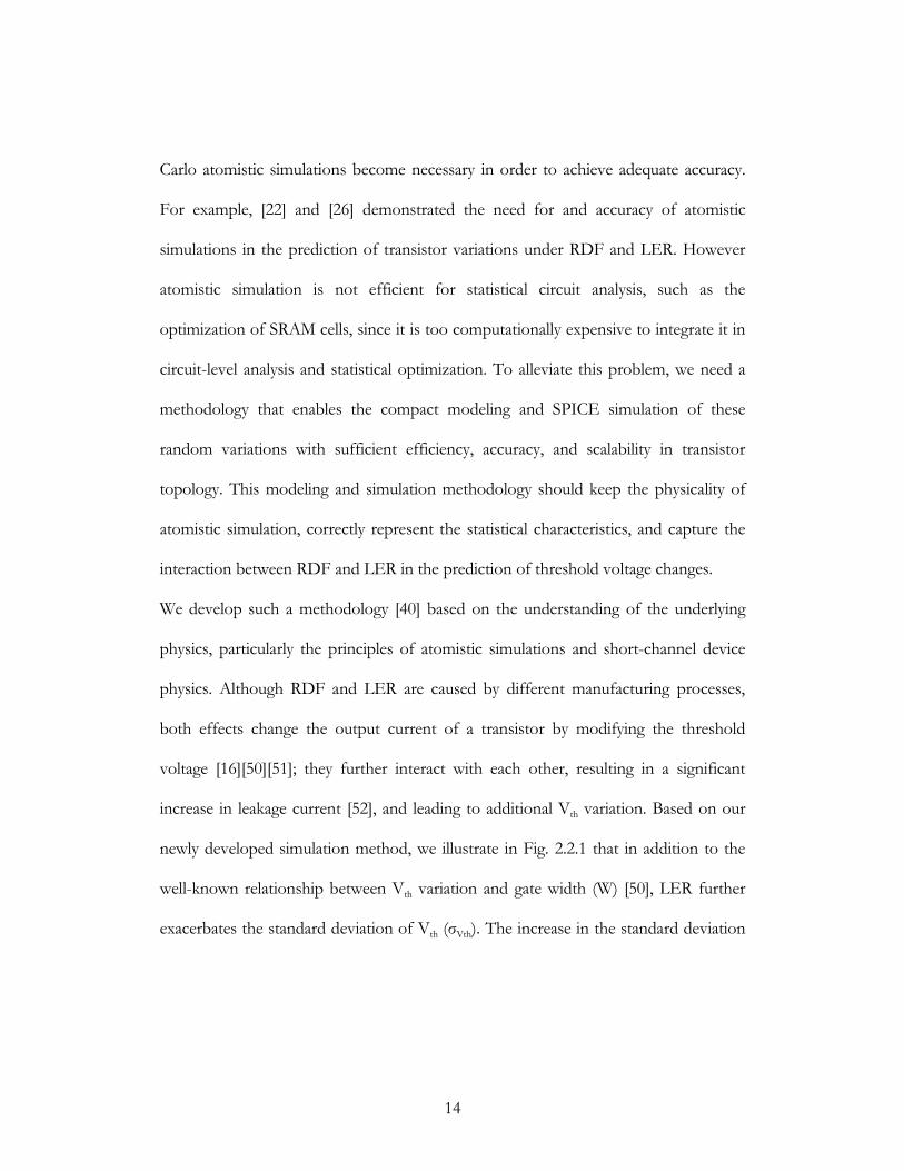
newly developed simulation method, we illustrate in Fig. 2.2.1 that in addition to the
well-known relationship between Vth variation and gate width (W) [50], LER further
exacerbates the standard deviation of Vth (σVth). The increase in the standard deviation

15
of Vth is more pronounced when the transistor width is small, which is the typical
condition in SRAM design.
We systematically validate the proposed method with available atomistic simulation
results under various conditions, including different amount of LER variations and
various transistor sizes. This part is organized as follows: Section 2.2.2 presents the
new gate slicing method, as well as the theoretical background from atomistic
simulation and device physics, identifying the appropriate slice width and transistor
operating region for gate slicing and Vth extraction, respectively. As verified with
atomistic simulations, the new SPICE simulation method is shown to accurately
predict the variability of saturation current (Ion), leakage (Ioff), and Vth. Based on the
method, we investigate the interaction of RDF and LER on Vth variation in Section
2.2.3 and show that while the high spatial-frequency component of LER only slightly
affects the mean value of Ioff, low frequency LER has a significant impact on both the
average and the distribution of the leakage and Vth. We propose a compact model to
directly calculate σVth from RDF and LER and further illustrate the interaction with
NRG and RNWE. Finally, we project the trend of Vth variation toward future
technology generations.

16
2.2.2 Gate-Slicing Method
In this section, we present the theoretical background and the flow of the proposed
method. The practicality and limitations of gate slicing are explained from the
physical principles. To handle the random effects of RDF and LER and predict Vth
variation from a given gate geometry, we split a non-uniform device into slices,
which have an appropriate slice width (d) that is larger than the correlation length of
RDF, but small enough to track the low frequency LER. Each slice is then modeled
as a sub-transistor with correct assignment of narrow-width and short-channel
effects, as shown in Fig. 2.2.2 [52][53]. Such a representation maps a non-uniform
transistor into a column of transistors which can easily be implemented in SPICE. It
well captures the statistical characteristics of a transistor under RDF and LER with
sufficient simulation efficiency.
After splitting the original non-uniform transistor into a column of rectangular ones,
the gate slicing method assigns different Vth values to different slices, and then sum the
drive current from each slice to analyze the total output characteristics. In order to
Figure 2.2.2. The flow to divide a non-uniform gate into slices. Each
slice has a unique Vthi and Li due to RDF and LER.
d

17
perform the linear superposition of currents, it requires that the drive current should
be a linear function of Vth. We satisfy this condition by extracting Vth from the strong-
inversion region, rather than the sub-threshold region. Because of the pronounced
velocity saturation effect, the output current in the strong-inversion region is a linear
function to Vth [16]. Therefore, it provides a correct mathematical basis to partition the
channel dopant under RDF, and then linearly superpose them together to monitor the
overall change in Vth. Combining this approach with the Equivalent Gate length (EGL)
model that describes the nominal device behavior under non-rectangular gate effect
[53], we are able to predict the amount of Vth variation under any given transistor
characteristics (e.g., non-rectangular gate, reverse narrow-width effect, etc.). The
section below further discusses the limitations of the new method in details.
Limitation on parallel slicing
By partitioning the non-uniform gate into parallel slices along the source-to-drain
direction (Fig. 2.2.2), the first underlying assumption is that the current in each slice
maintains the same direction from source to drain, i.e., there is no significant
distortion of the electrical field along the channel direction. Otherwise, there would
be a pronounced amount of current across the slice boundary and the slicing method
is not able to provide a correct prediction under LER [52][54]. To validate this
assumption, a 3D TCAD simulation using Sentaurus [55] is performed in Fig. 2.2.3,
with a typical 65nm device (gate length at 41nm and gate width at 50nm). From the
simulated result, the direction of the current density is not severely affected under

18
the LER effect. The current deviated to the width direction is much smaller than the
primary current along the channel direction and thus, can be ignored in the analysis.
With the aggressive scaling of both channel length and channel width, more
physical effects, such as DIBL and the fringe field from the gate edge, will affect the
channel region. The distortion of the electric field may be exacerbated in the extreme
case. If the current along the width direction becomes comparable to the current
along channel direction, then the gate slicing method has to be corrected.
Limitation on slice width
Even if the assumption of parallel slicing is true, there are still fundamental
limitations on slice width in this approach, especially when we consider the effect of
random dopant fluctuations, which usually requires atomistic simulation to provide
sufficient accuracy:
Figure 2.2.3. Simulated current density of a 65nm gate under severe LER (Vds=Vgs=1.1V).
Sou
rce
Dra
in
19
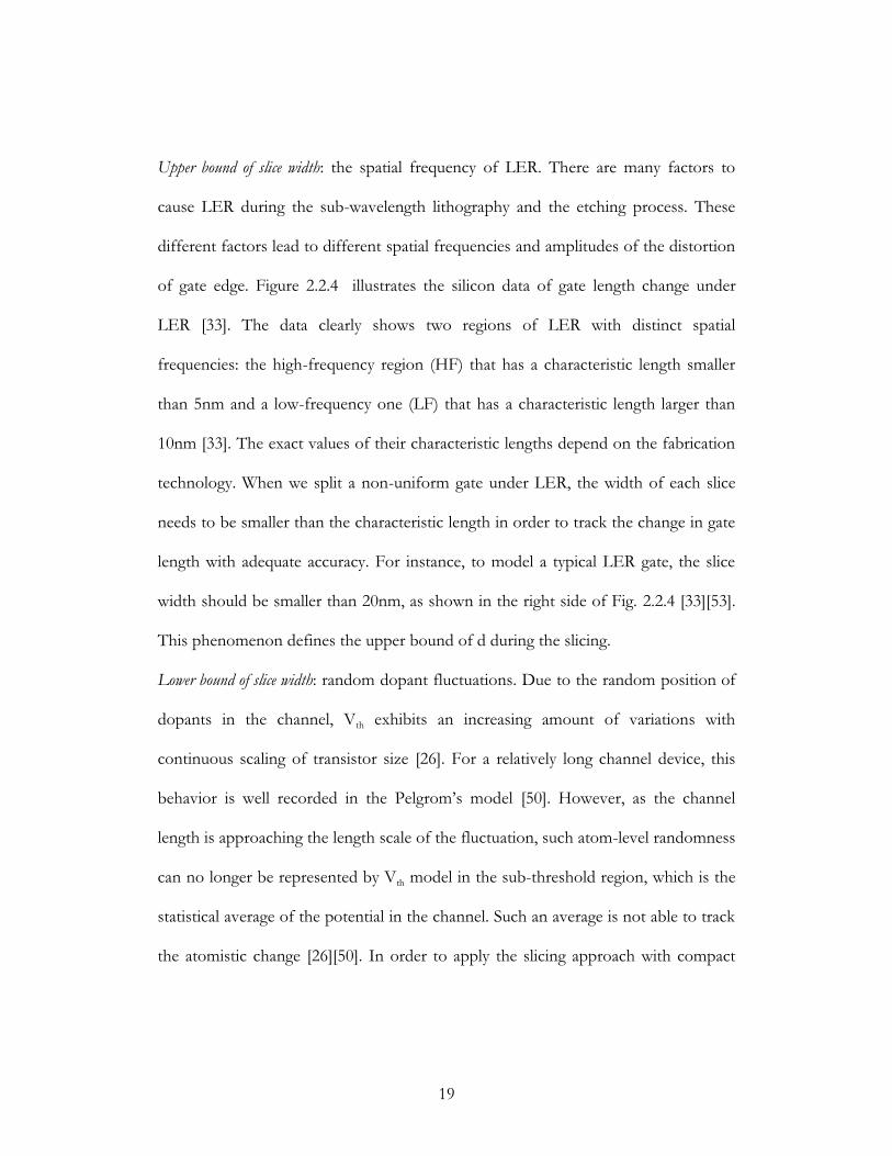
Upper bound of slice width: the spatial frequency of LER. There are many factors to
cause LER during the sub-wavelength lithography and the etching process. These
different factors lead to different spatial frequencies and amplitudes of the distortion
of gate edge. Figure 2.2.4 illustrates the silicon data of gate length change under
LER [33]. The data clearly shows two regions of LER with distinct spatial
frequencies: the high-frequency region (HF) that has a characteristic length smaller
than 5nm and a low-frequency one (LF) that has a characteristic length larger than
10nm [33]. The exact values of their characteristic lengths depend on the fabrication
technology. When we split a non-uniform gate under LER, the width of each slice
needs to be smaller than the characteristic length in order to track the change in gate
length with adequate accuracy. For instance, to model a typical LER gate, the slice
width should be smaller than 20nm, as shown in the right side of Fig. 2.2.4 [33][53].
This phenomenon defines the upper bound of d during the slicing.
Lower bound of slice width: random dopant fluctuations. Due to the random position of
dopants in the channel, Vth exhibits an increasing amount of variations with
continuous scaling of transistor size [26]. For a relatively long channel device, this
behavior is well recorded in the Pelgrom’s model [50]. However, as the channel
length is approaching the length scale of the fluctuation, such atom-level randomness
can no longer be represented by Vth model in the sub-threshold region, which is the
statistical average of the potential in the channel. Such an average is not able to track
the atomistic change [26][50]. In order to apply the slicing approach with compact

20
Vth-based device model, the slice width must be larger than the correlation length of
random channel potential near the threshold. This length is typically around several
nanometers, depending on the doping concentration [14]. The left side of Fig. 2.2.4
shows this lower bound of d during the slicing. If d is smaller than the correlation
length, then Vth model is not a correct representation of the statistical device
behavior under the RDF effect, particularly for the sub-threshold current [26].
Considering these two limits, Fig. 2.2.4 illustrates the appropriate region of d where
the slicing approach is applicable. Only when d satisfies both limits (i.e., the middle
region in Fig. 2.2.4), the partition of a single LER transistor is meaningful in physics
to predict the current in all regions. Note that the lower region, which is limited by
RDF, usually overlaps with that of the HF component of LER. Therefore, the slicing
method may work well for RDF and LF LER, but not RDF and HF LER. Since the
Si dataError! Reference
Limited by LER
Limited by RDF
HF LER
LF LER
1 10 1000.0
0.5
1.0
1.5
2.0
2.5
3.0
3.5
� L of L
ER (n
m)
Gate Slice Width d (nm)
Figure 2.2.4. The appropriate selection of slice width under both effects of RDF and LER [33].

21
L distribution under LER approximately follows the Gaussian function [33][53], we
use the correlation length of LER (Wc) as the slice width in the experiments
[56][57][58].
With the limitation, the slicing method is only valid in the case that the correlation
length of LER is larger than the correlation length of random potential due to RDF.
If people improve the etching process to reduce the LER correlation length, the
method to track LER shape should be revised.
Limitation on operation region
After appropriately slicing the gate with a non-rectangular shape, we can describe the
characteristic of each slice using compact device model. The summation of all the
slices provides the behavior of the original LER gate. For the nominal condition,
each slice has different Vth from the deterministic effects of narrow-width and DIBL.
They lead to the increase in the leakage current and the reduction in the effective
gate length. The changes of Ion and Ioff under these effects are well captured through
the Equivalent Gate Length (EGL) model [53], i.e., a smaller Lmin for Ioff and a larger
Lmax for Ion. In this work, we follow the same modeling approach to formulate the
nominal transistor model.
However, the situation becomes much more complicated when we incorporate
statistical variation due to random dopant fluctuation into each slice. Since Ioff is an
exponential function of Vth (Fig. 2.2.5), which is very non-linear, the linear
superposition of Ioff from each slice is not applicable and thus, the mean and
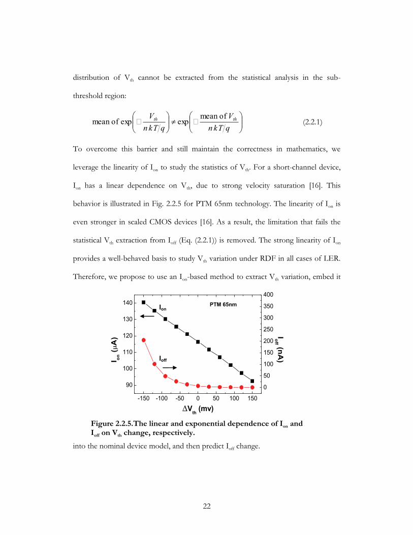
22
distribution of Vth cannot be extracted from the statistical analysis in the sub-
threshold region:
���
�
�� ��
�
�
��
qkTnV
qkTnV thth ofmean
expexp ofmean (2.2.1)
To overcome this barrier and still maintain the correctness in mathematics, we
leverage the linearity of Ion to study the statistics of Vth. For a short-channel device,
Ion has a linear dependence on Vth, due to strong velocity saturation [16]. This
behavior is illustrated in Fig. 2.2.5 for PTM 65nm technology. The linearity of Ion is
even stronger in scaled CMOS devices [16]. As a result, the limitation that fails the
statistical Vth extraction from Ioff (Eq. (2.2.1)) is removed. The strong linearity of Ion
provides a well-behaved basis to study Vth variation under RDF in all cases of LER.
Therefore, we propose to use an Ion-based method to extract Vth variation, embed it
into the nominal device model, and then predict Ioff change.
Figure 2.2.5.The linear and exponential dependence of Ion and Ioff on Vth change, respectively.
-150 -100 -50 0 50 100 150
90
100
110
120
130
140
�Vth (mv)
I on (�
A)
0
50
100
150
200
250
300
350
400
Ioff (nA)
Ion
Ioff
PTM 65nm

23
Finally, we should note that the inaccuracy of Ioff-based extraction method also
depends on the size of the transistor: the smaller the slice is, the larger Vth variation
will be; the error caused by the non-linearity (Eq. (2.2.1)) is then more pronounced.
On the other hand, if the slice size is large enough, then the difference in Vth among
slices becomes smaller and the Ioff-based modeling error is reduced.
Saturation Current (Ion)-Based Method
Based on the discussion above on the limitations of gate slicing method, we propose
Figure 2.2.6. The flow to generate a single device model for statistical analysis of a LER gate.
Statistical single transistor model by integrating new σVth and EGL models
Extraction of Vth variation from Ion
A non-rectangular gate shape with σL due to LER and σVth due to RDF
Equivalent Gate Length model for nominal I-V characteristics
Gate slicing at appropriate slice width
Assignment of random Vth to each slice depending on its W, L, and σVth

24
the saturation current (Ion) based method to investigate the interaction of RDF and
LER induced variations in circuit simulation.
Figure 2.2.6 summarizes this flow that supports the development of a single device
model for statistical analysis under RDF and LER. The method starts from the
distorted gate shape with LER. With the given shape, the statistical channel length
variations and the correlation length of the gate edge is extracted for circuit
simulation. Then we divide it into slices with a suitable width, following the guidance
in Fig. 2.2.4. Next, the model of EGL is produced for the nominal case under the
non-uniform gate [53]. To investigate the interaction with RDF on Vth variation, we
assign Vth to each slice as a statistical variable. While its mean value is determined by
the width and length of the slice (i.e., RNWE and DIBL effect) [53], its standard
deviation also depends on the size of the slice [22][50][51]:
WLthV1
�� (2.2.2)
The exact value of σVth due to RDF is technology dependent [3]. From the
summation of Ion, we finally extract the variation of the threshold voltage of the
entire transistor under LER and RDF. Since the length of each slice is different
under LER, such non-linear relation between σVth and L (Eq. (2.2.2)) leads to an
increase in Vth variation of the entire transistor, as demonstrated in Fig. 2.2.1. With
the extracted threshold voltage variation, we apply the Equivalent Gate Length
model [53] for the sub-threshold region to obtain the Ioff variations, with the
validated assumption that the sub-threshold slope can be treated as a constant for
25
typical LER variation in the nanometer regime [34]. The outcome is a single device
model with EGL and a new σVth, which supports efficient statistical performance
analysis for any given LER and RDF.
2.2.3 Validation with Silicon Data
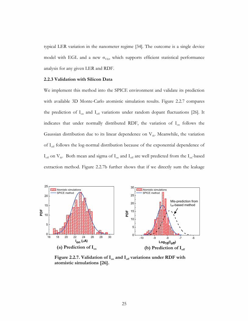
We implement this method into the SPICE environment and validate its prediction
with available 3D Monte-Carlo atomistic simulation results. Figure 2.2.7 compares
the prediction of Ion and Ioff variations under random dopant fluctuations [26]. It
indicates that under normally distributed RDF, the variation of Ion follows the
Gaussian distribution due to its linear dependence on Vth. Meanwhile, the variation
of Ioff follows the log-normal distribution because of the exponential dependence of
Ioff on Vth. Both mean and sigma of Ion and Ioff are well predicted from the Ion-based
extraction method. Figure 2.2.7b further shows that if we directly sum the leakage
16 18 20 22 24 26 28 300
5
10
15
20
25
Atomistic simulations SPICE method
Ion (�A)
Figure 2.2.7. Validation of Ion and Ioff variations under RDF with atomistic simulations [26].
(a) Prediction of Ion (b) Prediction of Ioff
-10 -9 -8 -7 -60
5
10
15
20
25
30
Atomistic simulations SPICE method
Log10(Ioff)
Mis-prediction from Ioff-based method

26
current from every slice to estimate Vth variation, it results in a significant error, as
indicated by Eq. (2.2.1).
In addition to the verification of the Ion-based method under RDF, Fig. 2.2.8
evaluates the prediction of σVth under different conditions of gate length variations
due to LER, assuming a uniform channel doping concentration (i.e., no RDF) [26].
Two devices are studied, with both gate width at 50nm, and gate length at 30nm and
50nm, respectively. The correlation length of the LER effect (Wc) is 20nm [26]. For
the low-frequency component of LER, the increase of σL results in a larger amount
of threshold variation, due to the interaction between σVth and L, as shown in Eq.
(2.2.2). This interaction is more pronounced when gate length is shorter, in which
case the threshold voltage of each slice is more strongly coupled with L through
DIBL effect [53].
As shown in Fig. 2.2.8, for a gate with the width of 50nm and the physical length of
30nm, which is typical for a SRAM transistor at the 65nm node, threshold variance
can be more than 20mV, purely due to the LER effect. Meanwhile, the nominal
Figure 2.2.9. Validation of σVth under both RDF and LER effects [26].
20 40 60 80 1000.0
0.1
0.2
0.3
0.4
0.5
LER only (�L=2nm)
RDF only
� log 10
(I off)
Effective Channel Length (nm)
Atomistic results SPICE results
RDF+LER
Figure 2.2.8. Validation of σVthunder LER .
0 1 2 3
0
5
10
15
20
�
Vth
(mV
)
�L (nm)
Atomistic simulations SPICE method
L=30nm
L=50nm
W=50nm

27
leakage current may increase by more than 15x due to LER at the same condition
[53]. Combining the information together, such effect will be a dominant factor to
impact the leakage and circuit stability at the worst case corner. Therefore, it is
crucial to incorporate accurate and efficient modeling capability into circuit
optimization, in order to mitigate the impact of LER. Our proposed approach
captures this complicated dependence very well, as compared to time-consuming
atomistic simulations. It is also ready to be integrated with circuit design tools. While
LER has a pronounced effect on Vth variation, the high-frequency component of
LER only has a marginal interaction with Vth variation. Since its spatial frequency is
quite high, its impact is averaged out across the slice [26]. Instead, it mainly affects
the mean value of Ioff, which has been well modeled in the EGL model[53].
Finally Fig. 2.2.9 verifies the prediction of threshold variation in the presence of both
RDF and LER effects. The variation of Vth is evaluated through the distribution of
Ioff, which is very sensitive to Vth change due to its exponential dependence. Three
sets of experiments are carried out: LER only with σL at 2nm, RDF with a
rectangular gate (i.e., no LER), and RDF with the LER shape. Again, gate width is
fixed at 50nm. Since Vth depends on L through the DIBL effect [16][53]:
���
����
'exp0 l
LVVV dsthth (2.2.3)
where Vth0 is a function of channel doping, the change of Vth due to L variation and
RDF can be derived as:

28
''
exp0 lL
lLVVV dsthth
���
��
������ (2.2.4)
Therefore, the total variation of Vth follows the relationship below, as long as σL and
RDF are independent:
222LERRDFtotal ��� �� (2.2.5)
where σRDF, σLER, σtotal are Vth variations due to RDF only, LER only, and the total
amount, respectively. The contributions of LER and RDF are independent to the
statistics of Vth. The relationship is well verified with atomistic simulations, as shown
in Fig. 2.2.9.
Figure 2.2.9 indicates that when L is large, RDF is the dominant factor in threshold
variation. As gate length decreases, the importance of LER rapidly increases in the
calculation of Vth variation. Again, the main reason is the strong DIBL effect, which
is an exponential function of L, as shown in Eq. (2.2.3). Overall, our Ion-based
simulation method provides excellent predictions of Vth variation under all situations,
as compared to 3D Monte-Carlo atomistic simulation results. It significantly
enhances the simulation efficiency, with fully compatibility to circuit simulators.
2.2.4 Interaction with Non-Rectangular Gate and Reverse Narrow Width
Effects
The Ion-based gate slicing method is general to study different types of gate distortion,
including the non-rectangular gate (NRG) effect due to sub-wavelength lithography
[53]. This section investigates the variations under NRG and RNWE effects at 65nm.

29
Different from statistical LER and RDF effects, NRG is relatively deterministic: the
gate shape under NRG can be predicted from the layout and lithography
specification. In reality, systematic NRG and random LER effects exist together in
the post fabrication process, as shown in Fig. 2.2.10. They change the nominal Ion
and Ioff values, as well their variations; the exact shift depends on the shape,
especially when RNWE is pronounced.
The RNWE effect non-uniformly reduces the threshold voltage in different locations:
the closer a gate slice is to the gate end, the larger Vth drop is. Such non-uniformity
along the width direction interacts with NRG and varies the output current
[52][53][54]. For instance, when the minimum channel length is close to the gate
extension, the threshold drop due to DIBL will strength the drop due to RNWE,
leading to the worst leakage increase; on the other hand, if the maximum channel
length locates closely the gate end, then DIBL and RNWE compensate each other
Figure 2.2.10. The illustration of NRG plus LER in a gate.
(a) Ideal layout (b) NRG (c) NRG plus

30
on Vth change. Figure 2.2.11a shows these two representative conditions of gate
shape distortion, in which both shapes have the same nominal L and the same
magnitude of NRG and LER; but one is convex and the other is concave and thus,
they are different in RNWE.
Based on the RNWE model [52][53] and the new Ion-based method, the impact of
NRG and RNWE on Vth variation is investigated in the presence of LER and RDF.
Figure 2.2.11 shows Vth variations under various LER amplitudes and spatial
frequencies, covering three types of transistors, i.e., an ideal rectangular gate and two
NRG shapes in Fig. 2.2.11a. While NRG and RNWE significantly affect the nominal
value of Ioff [53][52], σVth is relatively insensitive to RNWE, since RNWE only shifts
Figure 2.2.11. Threshold variation under NRG and RNWE.
(a) Two representative gate distortions under NRG
Shape 1 S Shape 2 D S D
Gate Gate
(b) Vth variation under various LER spatial frequencies
(c) Vth variation under various amount of LER
0 5 10 15 205
10
15
20
� Vth
(mV)
W/Wc
w/o NRG w/ NRG: shape 1 w/ NRG: shape 2
�L=1.5nmNRG magnitude:Leff_max=31.7nm, Leff_min=17.3nm
0.0 0.5 1.0 1.5 2.0
0
5
10
15
W/Wc=10NRG magnitude:Leff_max=31.7nm, Leff_min=17.3nm
� V th
(mV)
�L (nm)
w/ NRG w/ NRG shape 1 w/ NRG shape 2
31
the mean value of Vth, but does not induce any variations. Figure 2.2.11 confirms this
result as there is no difference in σVth between shape 1 and shape 2. On the other
hand, the magnitude of NRG impacts both DIBL and σVth (Eq. (2.2.2)). Therefore,
it interacts with LER on Vth variation, although the exact NRG shape does not
matter because of the insensitivity to RNWE.
2.2.5 Predictive Modeling of Threshold Variation
Based on the underlying physical mechanisms, we successfully develop the SPICE
simulation method from gate slicing to the extraction of Vth variation in the strong
inversion region. In this section, we further propose a compact model that directly
predicts Vth variation from RDF and LER. This model updates traditional Pelgrom’s
model with additional consideration of the LER effect. Using this model, we
extrapolate the variation of Vth towards future technology nodes, helping shed light
on robust circuit design with scaled CMOS technology.
Modeling of Threshold Variation
For traditional long-channel device, Vth mismatch is mainly induced by random
effects, such as the dopant fluctuation. This consideration is the basis for the well
known Pelgrom’s model and other Vth variation models, in which σVth is inversely
proportional to the square root of the transistor size [3][22][50].However, as shown
in Figs. 2.2.9, the impact of LER on Vth variation becomes pronounced with further
scaling of L, and can no longer be ignored in the calculation of threshold mismatch.

32
These two effects superpose each other in the statistical property of Vth, as shown in
Fig. 2.2.9 and Eq. (2.2.5).
As presented in [22][50][51], random dopant fluctuations induce the deviation of Vth
as a linear function of (WL)-0.5. For a larger transistor, the random distribution of
dopants is averaged out in the modeling of Vth. Akin to this effect, the random
distribution of gate length under LER also leads to a linear function of W-0.5, and
since the longer gate width is, the more the length distortion is averaged out. On the
other hand, due to the DIBL effect, LER induced Vth variation has an exponential
dependence on L (Eq. (2.2.4)). Therefore, we derive the following formula based on
Eqs. (2.2.2), (2.2.4) and (2.2.5):
� �2
2
2212
'2exp' Lcdd
total WW
lLlVC
WLC �� ���� (2.2.6)
Figure 2.2.12. The contour of Vth variation at 65nm. 0
0.51
1.52
05
10
1520
0
5
10
15
20
25
σL W/Wc
�Vt
h (m
V)

33
where Wc is the correlation length of LER, and C1, C2 and l’ are technology
dependent coefficients. The coefficient l’ is the characteristic length of DIBL effect,
and it can be extracted from equations from BSIM parameter lt0 and DSUB. For
example, for 45nm technology, C1 is around 10-18V2·m2, C2 is around 1.5, and l’ is
around 10nm. The first term describes conventional Pelgrom’s model under RDF.
The second term is designated to the variation due to LER. The exponential
dependence on L is demonstrated in Fig. 2.2.9. Figure 2.2.12 demonstrates the
dependence of threshold variation on channel length variation and the correlation
length of LER; Fig. 2.2.13 further verifies Eq. (2.2.6) at different gate width. Our
model accurately captures the superposition of these two statistical components, as
well as the inverse square root dependence on W. Traditional model only considers
the RDF effect and thus, significantly underestimates the total amount of Vth
variation, as shown in Fig. 2.2.13. Note that due to the exponential dependence on L
of the second term in Eq. (2.2.6), the impact of LER diminishes at long gate length
(Fig. 2.2.9). Yet the second term rapidly affects threshold variation for a device with
short gate length and width. For instance, at W=50nm, it has a comparable influence
as that of RDF. Therefore, its role cannot be neglected, particularly when we design
the circuits with minimum size transistors in scaled technologies.

34
Projection to Future Technology Nodes
With solid verifications with atomistic and SPICE simulations, the proposed
compact model offers a scalable tool to explore threshold variation under LER and
RDF effects. As shown in Fig. 2.2.9 and 2.2.11, this approach has the right sensitivity
to the transistor definition, as well as the amount of variations. In this section, we
extrapolate these models to future technology generations [16], with the goal to gain
early stage insights to robust design under increased variations.
Continuous scaling exacerbates both RDF and LER effects, as shown in Figs. 2.2.1
and 2.2.2. With the scaling of transistor size, the total number of dopants in the
channel significant reduces [75]. As a consequence, the amount of random RDF
effect becomes more significant (Fig. 2.2.1). For line-edge roughness, the
improvement is limited by the etching process, rather than the lithography process
[26][34]. The emerging etching technology may reduce 3σ of LER amplitude down
Figure 2.2.13. Validation of predictive modeling
with SPICE simulation using gate slicing method.
100 1000
10
20
30
�V
th
(mV
)
Gate Width W (nm)
SPICE simulationsModel
LER only
RDF only
LER+RDF
σL =2nm

35
to ~2nm [41][42][59][60] and the correlation length around 10~20nm [59][60]. Yet
such improvements still lag behind the scaling rate of nominal channel length.
Therefore, the sensitivity of device performance to LER dramatically increases at
recent technology nodes. Finally, the situation of NRG is not optimistic due to the
difficulty in photo-lithography. The distortion in gate length is expected to increase
[57][61], even though lithography recipes and layout techniques, such as regular
layout fabrics, may help improve the situation [57].
Using the new method, we project the amount of threshold variation, under possible
scenarios of RDF and LER. The nominal model file is adopted from PTM [16]. In
this projection, new technology advances, such as high-k and metal gate, are not
considered. Other potential variation sources, such as RDF induced mobility
variation [62], have not been included. Upon the availability of atomistic simulation
tools and experimental data, our SPICE-based method is extendable to those
additional factors. Table 2.2.1 summarizes the results for various LER parameters of
Table 2.2.1. Projection of threshold variation in traditional bulk CMOS devices
LER parameters Total σVth (mV)
Wc (nm) σL (nm) 65nm (Vds=1.1V)
45nm (Vds=1V)
32nm (Vds=0.9V)
22nm (Vds=0.8V)
5 0 19.4 27.5 37.9 55.7
0.5 19.5 27.8 38.9 57.9
1 19.9 28.8 42.1 63.7
10 0 19.4 27.5 37.9 55.7
0.5 19.6 28.1 40.0 59.9
1 20.3 29.9 45.8 71.3 W/L=2

36
Wc and σL. Even under the same amount of LER, the variation of the threshold
voltage keeps increasing due to the aggressive scaling of the feature size and the
exacerbation of short-channel effects. As the trend goes, future design will suffer a
dramatic amount of random Vth variation, leading to severe degradation in circuit
matching property, memory stability, and the leakage control. While the
improvement of process technology will continue, its effectiveness may be limited in
the future; therefore, innovative circuit design and optimization techniques are
critical to overcome these barriers.
2.2.6 2-D Slicing Method for RDF
As the device size continuous scales down. Compared to the device feature size, the
correlation length of LER and RDF is becoming more severe. Usually to simulate
such variations, 2-D or 3-D TCAD simulation is required. However, TCAD is time
consuming, inflexible, and difficult to calibrate, while SPICE based model is more
reliable and easier to calibrate. To increase the flexibility of the gate slicing method, it
is desired to extend the gate slicing method to two dimensional. On the other hand,
the 1-D gate slicing method we discussed in last chapter has limitations. For example,
the width of each slice cannot be two small; the modeling of RDF is not based on
potential profile so the method can only based on strong inversion region. If we can
extend the 1-D slicing method to 2-D, then we are able to model random potential
profile due to RDF, and we will not be limited by slice width and operating region.
The basic idea of the 2-D gate slicing is demonstrated in fig. 2.2.14. In this method

37
the start point is a square mesh of the MOS channel. In a turned on MOS transistor,
the square mesh is modeled by a black box with current coming in or going out
through four edges. Then in order to model the black box a 4-terminal unit in
SPICE is proposed as in fig. 2.2.14, inspired by the modeling method for substrate
noise[63]. The unit is built up with 4 simplified MOS transistors. They have a
common node connected, with other four nodes modeling the four direction current
Figure. 2.2.14. Demonstration of 2-D gate slicing method

38
in/out. To model RDF the surface potential of each mesh is calculated according to
the dopants distribution and the position of the mesh. Then with MONTE CARLO
simulations, we are able to investigate the Vth variation induced by RDF.
To model the transistor in a 4-terminal unit, a simplified BSIM IV model for DC
Channel charge and sub-threshold
swing models
Long channel Vth model Bulk charge model
Unified mobility model
Velocity saturation model
Simplified DC IV
model for MOS mesh
Figure 2.2.15. Demonstration of (a) Simplified BSIM IV model for
DC simulation and (b) Modeling of DIBL effect
(a)
(b)
Gate
Source Drain
� �� �'sinh
'sinh)( / lLlyVyV DS��
y

39
simulation is introduced in the experiments. Only the first order effects are taken
into account for the simplified mesh. The simplified transistor consists of channel
charge and sub-threshold swing models, the unified mobility model, and the
threshold voltage model without short channel/DIBL and Narrow width effect. To
model the behavior in saturation region the velocity saturation is incorporated by
introducing saturation voltage vdsat. If the voltage induced by drain bias is larger than
vdsat, then the mesh change saturation region. Because the voltage across channel
area increases monotonically along the source-to-drain direction, the saturation point
can be automatically solved by the circuit simulator. Inside the saturation region the
voltage and voltage drop is much larger than other region. To the first order we
model this part by setting the electrical field a constant larger value than the
saturation point.
In this work Verilog-A is used to build the mesh for simulation. To model the short
channel effect (SCE) and drain induced barrier lowering (DIBL) effect, the following
equation is incorporated:
� �� �'sinh
'sinh)( / lLlyVyV DS�� (2.2.7)
40
where ∆V(y) is the surface potential change along the channel, VS/D is the voltage on
source/drain side, including built-in voltage, l’ is characteristic length of DIBL, and L
is channel length. DIBL effect cannot be modeled inside the mesh itself. We model
the impact on each mesh by assigning the surface potential change according to its
position. Figure 2.2.15 demonstrates the simplified BSIM model and the modeling
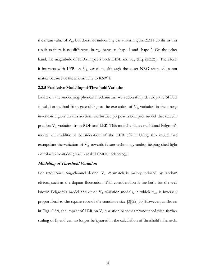
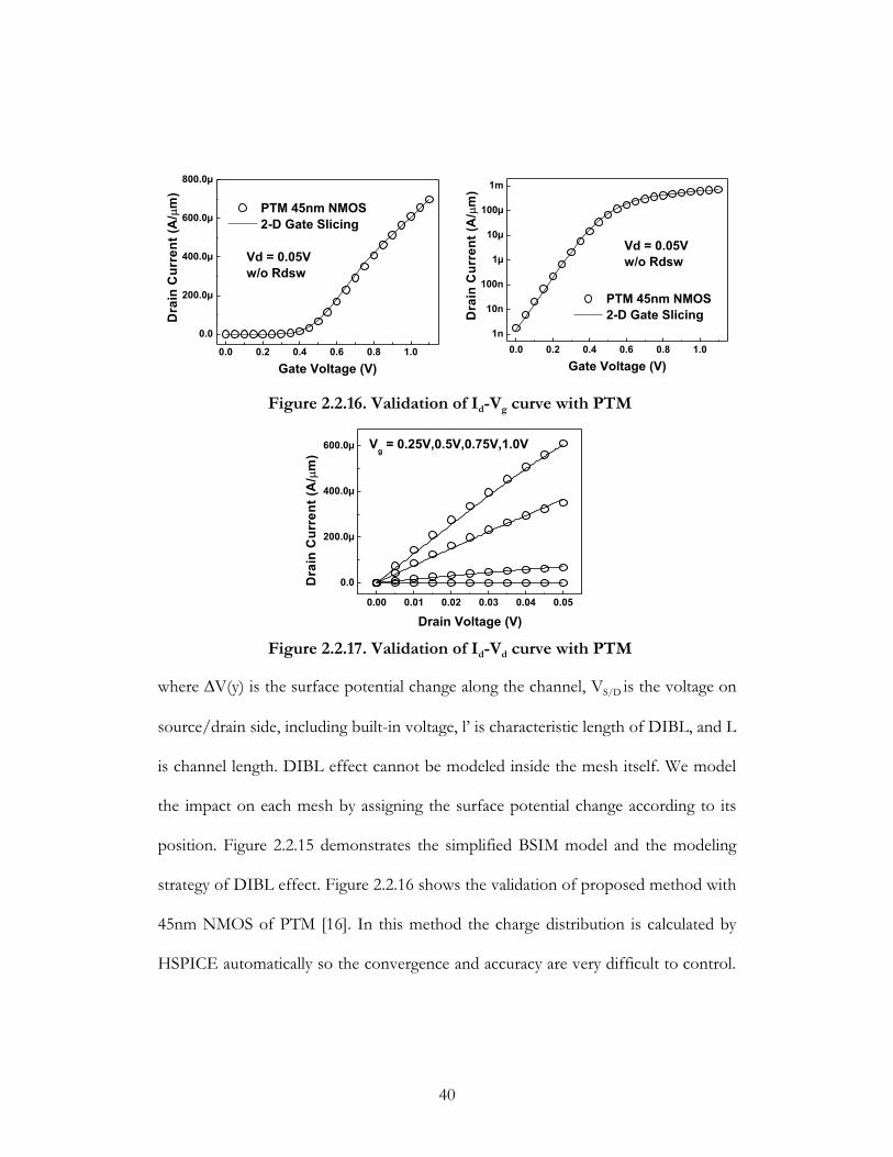
strategy of DIBL effect. Figure 2.2.16 shows the validation of proposed method with
45nm NMOS of PTM [16]. In this method the charge distribution is calculated by
HSPICE automatically so the convergence and accuracy are very difficult to control.
0.0 0.2 0.4 0.6 0.8 1.0
0.0
200.0μ
400.0μ
600.0μ
800.0μ
PTM 45nm NMOS 2-D Gate Slicing
Dra
in C
urre
nt (A
/�m
)
Gate Voltage (V)
Vd = 0.05Vw/o Rdsw
0.0 0.2 0.4 0.6 0.8 1.01n
10n
100n
1μ
10μ
100μ
1m
PTM 45nm NMOS 2-D Gate SlicingD
rain
Cur
rent
(A/�
m)
Gate Voltage (V)
Vd = 0.05Vw/o Rdsw
Figure 2.2.16. Validation of Id-Vg curve with PTM
Figure 2.2.17. Validation of Id-Vd curve with PTM
0.00 0.01 0.02 0.03 0.04 0.05
0.0
200.0μ
400.0μ
600.0μ
Dra
in C
urre
nt (A
/�m
)
Drain Voltage (V)
Vg = 0.25V,0.5V,0.75V,1.0V
41
However the low drain voltage region can achieve good accuracy. In fig. 2.2.17 the
Id-Vd curves under low drain voltage and various gate biases are validated with PTM
data.
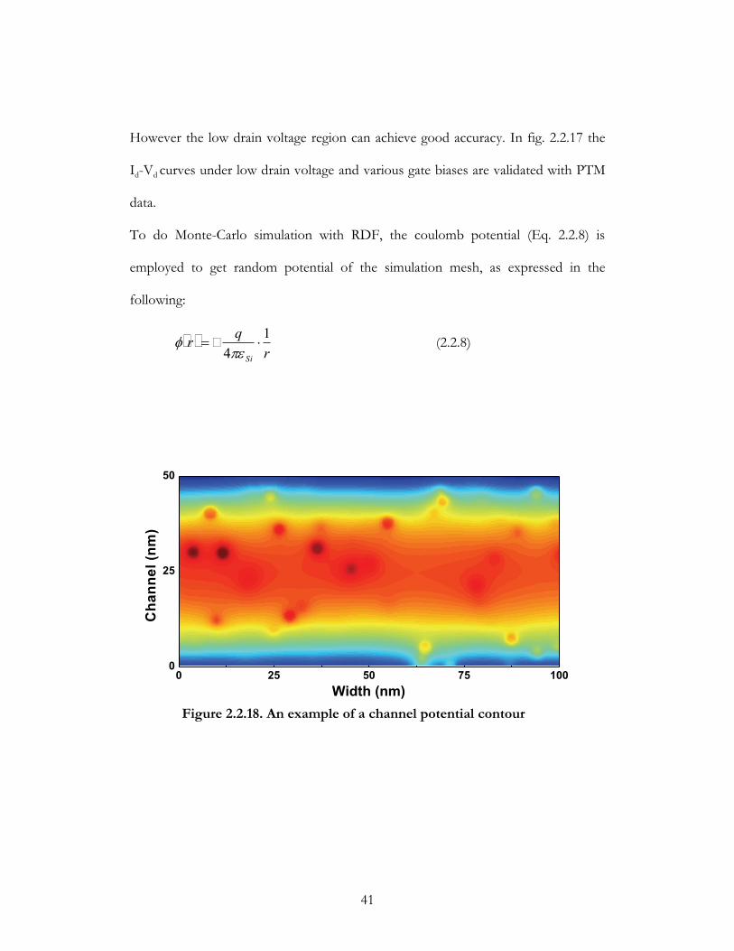
To do Monte-Carlo simulation with RDF, the coulomb potential (Eq. 2.2.8) is
employed to get random potential of the simulation mesh, as expressed in the
following:
� �r
qrSi
14
�����
� (2.2.8)
Figure 2.2.18. An example of a channel potential contour
0 25 50 75 1000
25
50
Cha
nnel
(nm
)
Width (nm)

42
where r is the distance to the center of atom. The coulomb potential can be splited
into short range and long range. Short range potential accounts for scattering, while
long rage part contributes to channel potential. Due to the singularity of the
expression, usually people do not take into account the short range part to calculate
channel potential. In this work, an empirical cut [26] is made to incorporate the long
range coulomb potential in the simulation. Note that at this stage the mobility
fluctuation due to RDF is not included. Figure 2.2.18 demonstrates an example of an
extracted potential fluctuation due to RDF in channel area. By simply change BSIM
parameter φs according to channel potential distribution we simulated the IV
variability with the proposed 2-D SPICE based simulation method. Figure 2.2.19
Figure 2.2.19. Simulated Id-Vg curves and corresponding Vth of 350 samples
0.0 0.2 0.4 0.6 0.8 1.01p
10p
100p
1n
10n
100n
1μ
10μD
rain
Cur
rent
(A)
Gate Voltage (V)
W=20nmL=17.5nmUniform DopingNch = 3.24e18cm-3
0.0 0.2 0.4 0.6 0.8 1.00.0
5.0μ
10.0μ
15.0μ
W=20nmL=17.5nmUniform DopingNch = 3.24e18cm-3
Dra
in C
urre
nt (A
)
Gate Voltage (V)
300 350 400 450 5000
10
20
30
40
50
60
Cou
nt
Vth (mV)
� = 378.2mV� = 34.5mV
350 400 450 500 550 6000
10
20
30
40
50
60
Cou
nt
Vth(intercept) (mV)
� = 489mV� = 38.5mV

43
shows the simulated Id-Vg curves and corresponding Vth distributions with 350
iterations.
2.2.7 Summary
Random variation in the threshold voltage is prominent in scaled CMOS technology
and severely affects circuit stability as well as performance distribution. The main
contributors include random dopant fluctuations, line-edge roughness, and other
non-idealities. Instead of using 3D Monte-Carlo atomistic simulations, we propose
an efficient simulation method in the SPICE environment that accurately captures
the impact of RDF and LER on Vth variation. The development of the new method
is based on the physical understanding of the underlying principles. In our method, a
non-uniform gate is first divided into appropriate slices; then threshold variation is
assigned and extracted from the strong-inversion region, with the benefit from the
linear dependence of Ion on Vth. The method significantly alleviates the computation
cost, providing sufficient fidelity to atomistic simulations and scalability to process
and design conditions. Based on this method, we further incorporate the impact of
LER into traditional Pelgrom’s model, identifying the exponential dependence on
gate length. With continuous scaling towards the 22nm node, the effect of RDF and
LER on Vth variations becomes even more critical for future robust design
exploration. Our method and compact model provide a physical and efficient tool
for statistical circuit performance analysis and optimization. In the end the early
exploration to extend the proposed gate slicing method from one dimensional to two

44
dimensional is presented. The proposed 2-D SPICE based slicing method works well
in low drain current region. More efforts are needed to improve this method to work
in all operating region and to capture the RDF induced mobility fluctuations.
2.3 Predictive Modeling of Fundamental CMOS Variations under Random
Geometry and Charge Fluctuations
2.3.1 Introduction
As CMOS continue scales into sub-20nm regime, besides RDF and LER, OTF and
RTN come to people’s sight due to its increasing impact on transistors. In this work,
atom-level TCAD simulations incorporating the four intrinsic variations are performed.
With the assistance of long range potential based equivalent charge density model [64],
RDF effect is simulated in commercial TCAD device simulator [55]. RTN, which is
from the trapping-detrapping of electron/hole, can be modeled as the occupation of a
single charge near the Si-SiO2 interface. Moreover, the geometric roughness of LER
and OTF are generated by Inverse Fourier Transform (IFT) from power spectrum
[36][44], which are further implemented into device simulator. Figure 1 shows the four
Preparation of Atomistic Simulation
Customized TCAD simulation under RDF, LER, OTF, and RTN
Predictive Modeling of Vth variations
Performance Projection and Optimization
Figure 2.3.1. The simulation and modeling flow

45
variation sources and their simulation setup. With the TCAD simulation result and the
understanding of fundamental physics, a new set of predictive compact models are
developed to capture the intrinsic Vth variability. Moreover, the predictive model
suggests the trend of Vth variations in scaling, and possible minimization method.
Figure 2.3.1 concludes the modeling approach in this work.
2.3.2 Atomistic Simulation of Fundamental Variations
Simulation Setup
The Monte Carlo simulations with 200 p-type MOSFETs are performed in this work.
The nominal simulation is calibrated with 22nm Predictive Technology Model (PTM)
[16]. The gate width is set to be 15nm. Moreover, to suppress the RDF as well as drain
induced barrier lowering (DIBL) effect, a retrograde doping profile is applied. For
RDF, both channel and source/drain dopants are taken into account. To simulate
discrete dopants in silicon body, an equivalent doping density profile is applied [64]:
32
3
)()sin(
2)(
rkrkqkr
c
cc
�� � (7)
where kc is the inverse of screening length, and r is the distance to the center of atom.
The gate edge profile of LER is generated by using IFT. To track the trend of
advanced technology, the correlation length of LER (Wc) is set as 10nm [42] and
standard deviation (σLER) equals 0.5nm [1][42]. The correlation length (λ) of oxide
surface roughness is 2nm [13], and the height of one Silicon atom layer (ΔH) is set to
be 2.71Å [13][44] for Si-SiO2 interface. RTN is usually studied in both time and

46
frequency domain. However, for a large scale circuit, such as SRAM, the statistical Vth
fluctuation due to RTN is also important because its lognormal distribution may
0 200 400 600 800 1000
Device No.200: 1 trap
Device No.2: 2 traps
Trap
Sta
te
Time (s)
Device No.1: 1 trap t High Level: OccupiedLow Level: Empty
Figure 2.3.2. Example of trap state in a CMOS
Figure 2.3.3. Simulated Id-Vg curves of 200 P-MOSFETs.
|Vds|= 0.05V, Gate Width = 15nm.
-0.8 -0.6 -0.4 -0.2 0.01E-13
1E-12
1E-11
1E-10
1E-9
1E-8
1E-7
1E-6
-0.8 -0.6 -0.4 -0.2 0.01E-13
1E-12
1E-11
1E-10
1E-9
1E-8
1E-7
1E-6
-0.8 -0.6 -0.4 -0.2 0.01E-13
1E-12
1E-11
1E-10
1E-9
1E-8
1E-7
1E-6
-0.8 -0.6 -0.4 -0.2 0.01E-13
1E-12
1E-11
1E-10
1E-9
1E-8
1E-7
1E-6
I ds (A
/15n
m)
Vgs (V)
Calibrated with PTM 22nm HP PMOS [11]Vds = 0.05VRDF only
Vgs (V)
LER only
I ds (A
/15n
m)
Vgs (V)
OTF only
Vgs (V)
RDF+LER+OTF

47
dominate the worse case of device performance.
In the time domain RTN effect due to a single trap is a Poisson process as Fig. 2.3.2
shows. To simulate the impact of RTN, we first model the characteristics of carrier
trapping-detrapping behavior by external codes, which give the trap distribution, as
well as the energy state for each trap. Then at any time point t from the simulated trap
state, the occupied trap is modeled by assigning a charge near the interface in device
simulation. Figure 2.3.2 shows examples of trap state in devices at time domain.
Different In the simulation, we assume a uniform distributed trap density, and uniform
distributed trap energy level around Ef [49]. The trap density is set to be 4e11 cm-2eV-1
[65]. Because RTN induced Vth variation is coupled with RDF, in the experiments, the
Vth variation solely induced by RTN is extracted from the same set of simulation with
and without random distributed traps.
Vth Variation
RDF LER OTF RTN0
10
20
30
40
�
Vth
(m
V)
S/D RDF only Body RDF only|Vds| = 0.05V
RDF+LER RDF+OTF LER+OTF Total0
20
40
�
Vth
(m
V)
TCAD Eq. (2)
(a)
(b)
Figure 2.3.4. (a) Simulated result of single source induced Vth
variation. (b) Vth variation due to combined sources.

48
200 devices are simulated in each experiment. Figure 2.3.3 shows the simulated Id-Vg
curves under various intrinsic variations. From first order we consider that σVth due to
each variation source are independent, and then we have the total σVth is
approximately a summation of each variation source as Eq. (8) shows.
2)(,
2)(,
2)(,
2)(,
2)(, RTNthOTFthLERthRDFthtotalth VVVVV ����� ���� (8)
Figure 2.3.4 summarizes the simulation result. From the simulation results, RDF is still
the major variation source. Note that RDF is contributed by both channel dopants and
source/drain dopants, and the fluctuation of body dopant is a major part in RDF
effect as Fig. 2.3.4 shows. LER induced variability is not that significant due to the
advanced etching technique as well as the retrograde doping with high peak
concentration, while OTF is the second important variation contributor. Moreover,
the contribution of RTN to total σVth is marginal. However, the lognormal distribution
Figure 2.3.5. Simulated ΔVth distribution and CDF due to a single occupied trap.
10 20 30 40 50 60 700.10.5
2103050709098
99.5
�Vth (mV)
CD
F (%
)
10 20 30 40 50 60 700
10
20
30
40
Cou
nt
�Vth (mV)
Worst case

49
of RTN induced Vth shift may be a problem for high-yield design. Figure 2.3.5 shows
the distribution and CDF of a single trap induced Vth shift, and it suggests that the
RTN induced large Vth shift may dominant the worse case of threshold voltage.
2.3.3. Predictive Modeling of Random Vth Variations
Based on the customized 3-D atomistic simulation result, in this section a new suite
of scalable models is derived. From first principles, the amount of Vth variation is
modeled in respect of Nch and toxe. The σVth due to RTN is not taken into account in
total Vth variation amplitude (Fig. 2.3.4). Because the RTN main dominant the worse
case of Vth variation, the distribution function of RTN induced Vth shift is included.
RDF
The RDF induced Vth variations are classified into body RDF and source/drain (S/D)
RDF. The body RDF, which is induced by fluctuation of substrate body dopants, is
the commonly studied one, and has been regarded as the dominant variation source in
device scaling. In our simulation of 22nm technology, the σVth due to body RDF is
35.2 mV, which is indeed the dominant one among all variations (Fig. 2.3.4). Different
from body RDF, S/D RDF, which arise from source/drain dopants, does not
contribute to gate voltage drop. As the device size scales to sub 25nm regime, the
fluctuation of S/D dopants leads to fluctuation of effective channel length [23] and
overlap capacitance [3]. From simulation results S/D RDF is a secondary factor that
contributes to Vth variation.
The Vth variation due to body RDF is expressed as the following equation [10]:

50
2.13
��WLWN
CqV depch
INVth�
(9)
where W, L, Nch, Wdep are the channel width, channel length, effective channel doping
(Nch) and depletion width respectively. In this model the non-uniformity along lateral
directions and fluctuation of Wdep are ignored, so there is a correction factor of 1.2.
Expanding the Wdep term and ignoring the second order terms, we have a more
explicit expression:
41
1)(2
3 ���
�
��
qNt
WLqCV chSi
ox
oxeRDFth
��
� (10)
where C1 is a fitting parameter accounts for surface potential and the correction term,
toxe, εSi, εox, and q are the equivalent oxide thickness, permittivity of Silicon, permittivity
of oxide layer, and elementary charge respectively. Equation (10) suggests that the
RDF induced Vth variation is proportional to toxe and Nch0.25. Figure 2.3.6 shows the
Figure 2.3.6. Nch and tox dependence of RDF induced σVth.
2x10¹⁹ 1x10¹⁹ 0
0
10
20
30
40
50
60
0.5 1.00
10
20
30
40
50
60
�Vth
(mV)
Model TCAD
|Vds| = 0.05VW = 15nmL = 13nm
Nsub (cm-3)
�Vth
(mV)
tox (nm)

51
simulated result compared with Eq. (10).
LER
To the first order, the nominal Vth shift due to short channel effect can be expressed
as in Eq. (11) and (6) [10]:
� �� � 1'cosh
221
���
���lLVV
V dssbith
� (11)
41
2' ��
�
�
���
ch
sSi
ox
oxeSi
qNt
l��
���
(12)
where Vbi is the built-in voltage of the source/drain junction, and η is a parameter to
model the average depletion width along channel. LER results in a fluctuation of
channel length. Assuming the two edges of gate are uncorrelated, the channel length
fluctuation due to LER is calculated by using the following equation [7]:
LERWW
Lc
�� ��
�/1
2 (13)
where σLER and Wc is the standard deviation and autocorrelation length gate edge
respectively. Equation (13) suggests that for a scaled device, the device feature size is
comparable or smaller than the spatial period of random gate edge, causing less
sensitivity of channel length variation to the device size. Differentiate Eq. (11), and
substitute Eq. (13), yields the following expression:
� � � �� �� �
LERWWlLl
lLVCV
c
dsLERth �� �
��
��
/12
1'cosh'2'sinh
22
)( (14)

52
41
32
' ���
�
���
ch
Si
ox
oxeSi
qNt
Cl�
��
(15)
where C2 is a fitting parameter in term of the voltage, which associated with junction
built-in voltage induced short channel effect. C3 is a fitting parameter associated with
surface potential, with the unit of V0.25. Figure 2.3.7 shows the comparison of model
and TCAD simulated results.
Figure 2.3.7. (a) Nch and tox dependence of LER induced σVth
(b) Vds dependence of LER induced σVth.
6.0x10¹⁸ 4.0x10¹⁸
16
18
20
22
24
26
0.8 1.0 1.2 1.4 1.6
20
25
30
35
40
45
TCAD MODEL
|Vds| = 0.8VW = 15nmL = 13nm
�Vth
(mV)
Nsub (cm-3)
�V th
(mV)
tox (nm)
0.0 0.2 0.4 0.6 0.8 1.0
16
18
20
22
TCAD Model
|Vds| = 0.8VW = 15nmL = 13nm
�Vth
(mV)
Vds (V)(b)
(a)
(b)

53
OTF
Similar to LER, OTF leads to the geometric fluctuation of the average oxide
thickness, and further affect gate voltage drop across the oxide layer. From the first
principle, Vth is expressed as the following:
sSichox
oxesFBth qNt
VV ���
� 2��� (16)
The oxide thickness is dependent on surface roughness between Silicon and Silicon
dioxide. The maximum fluctuation magnitude of oxide surface roughness is the
height of one silicon atom layer (ΔH) = 2.71Å. The correlation length (λ) of oxide
surface, which is typically from 1 to 3nm [23], is much smaller than gate length. With
the assumption that the two oxide surfaces are uncorrelated the sigma of oxide
thickness fluctuation is expressed in Eq. (17):
WLBHtox 2
�� �� (17)
Figure 2.3.8. Nch and tox dependence of OTF induced σVth.
0.8 1.0 1.20
10
20
30
40
2x10¹⁹ 1x10¹⁹ 00
5
10
15
20
25
�V
th (m
V)
tox (nm)
�V
th (m
V)
TCAD Model
|Vds| = 0.05VW = 15nmL = 13nm
Nsub (cm-3)

54
where λ denotes the correlation length of oxide surface roughness, and B is a fitting
parameter. Moreover, from Eqs. (16) and (17), the sigma of OTF induced Vth
variation is derived in Eq. (18):
HWL
qNCV
ox
Sichth ��
24�
��
� (18)
where C4 is a fitting parameter in terms of V0.5. Figure 2.3.8 validates this result.
From Fig. 2.3.8, OTF induced Vth is independent of oxide thickness. Moreover, the
dependence OTF induced Vth variation on Nch is more sensitive than RDF induced
variation, which suggest that as channel doping increasing in future CMOS device,
the trend of OTF induced Vth variation may be worse and dominate the variations of
device performance.
RTN
The interaction among RTN on RDF, LER, and OTF effects is investigated through
atomistic simulations in this sub-section. The structure used to determine the effects
of RDF, LER, and OTF are simulated with and without a single occupied trap in Si-
SiO2 interface. Figure 2.3.9 summarizes the comparison of Vth variation between
untrapped and trapped state of a single trap. From the plot, the impact of one
trapped carrier on σVth seems to be marginal. Therefore we assume that the Vth
variations due to the other three effects are independent on RTN.
The number of traps in a device follows the Poisson distribution with mean value
NtWL, where Nt is the trap density around Ef. Assume P is the average probability

55
that a trap is occupied, then the average trapped carrier number in a device is PNtWL,
and the probability density function of occupied trap number is:
� �...2,1,0
!)( ��
�
xxeWLPN
xfWLPNx
tt
(19)
A trapped carrier interacts with RDF effect will result in different amount of Vth shift.
The Vth shift due to single trapped carrier is expressed as [6]:
� �� � ��
�
�
��
���
kTCCVVqt
WLqV
oxd
thth
ox
oxeth 1
'exp
� (20)
where k is the Boltzmann constant, Cd is the depletion layer capacitance, and Vth’ is the
equivalent threshold voltage of the channel region that impacted by a trapped carrier.
From first order, Vth’ is induced by RDF, so according to Eq. (17) its variation is
proportional to toxe·Nch0.25. Regarding to Eq. (20), the ΔVth due to RTN of a single trap
is a lognormal random variable, which follows:
���
�
����
�
��� 4
1
5lognormal)( ,ln choxeox
oxeRTNth NtC
tWLqfV
� (21)
where C5 is a fitting parameter with the unit of V·cm-0.25, and flognormal is the lognormal
distribution function:
� �22
ln
lognormal 21),( �
�
����
��
�x
ex
f (22)
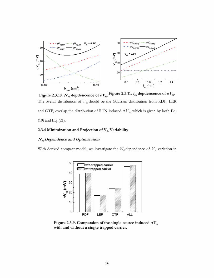
56
The overall distribution of Vth should be the Gaussian distribution from RDF, LER
and OTF, overlap the distribution of RTN induced ΔVth, which is given by both Eq.
(19) and Eq. (21).
2.3.4 Minimization and Projection of Vth Variability
Nch Dependence and Optimization
With derived compact model, we investigate the Nch dependence of Vth variation in
Figure 2.3.9. Comparsion of the single source induced σVth
with and without a single trapped carrier.
RDF LER OTF ALL0
10
20
30
40
50
�Vth
(mV)
w/o trapped carrier w/ trapped carrier
Figure 2.3.10. Nch depdencence of σVth.
1E18 1E19
20
40
60
�Vth
(mV)
Nsub (cm-3)
�Vth(RDF) �Vth(LER)
�Vth(OTF) �Vth(total)
Vds = 0.8V
Figure 2.3.11. tox depdencence of σVth.
0.6 0.8 1.0 1.2 1.4
20
40
60
80
Vds = 0.8V
�Vth(RDF) �Vth(LER)
�Vth(OTF) �Vth(total)
�Vth
(mV)
tox (nm)

57
Fig. 2.3.10. In the plot the Vth variation first decrease with Nch, because at low doping,
LER dominant the σVth. As the Nch continue increasing, the increasing in Vth
variation suggests that RDF and OTF dominates σVth in high doping region. From
the Nch dependence, the minimum σVth is found to around 2e18 cm-3. This fact
indicates that Nch optimization may be a possible method to minimize Vth variations.
Effect of tox Tunning
The tox dependence is shown in Fig. 2.3.11. Apparently, the Vth increase as the tox
increase. σVth is very sensitive to tox. So the strategy to reduce tox will be very effective
for suppressing threshold variation.
Scaling Trend of Vth Variation
Based on PTM HP model, a projection of Vth variation is illustrated in Fig. 2.3.12.
From Fig. 2.3.12, we observe that if there is little improvement in the etching process,
the LER induced Vth variation may approach the RDF induced Vth variation in
Figure 2.3.12. The trend of σVth in device scaling.
12nm 16nm 22nm 32nm 45nm0
20
40
60
80
�Vth
(mV
)
Technology Node
�Vth(RDF)
�Vth(LER)
�Vth(OTF)
�Vth(total)
Based on PTM [11]W/L = 2 with �-doping

58
future nodes. On the other hand, due to the square-root dependence of Nch, OTF
induced Vth variation shows a faster increasing rate during the scaling, and may
dominate the variability in future.
2.3.5 Summary
In this work, random Vth variation under RDF, LER, OTF and RTN is studied by
using 3-D atomistic simulation with commercial TCAD device simulator. With the
simulated result, a suite of scalable and predictive compact models are proposed.
Furthermore, possible solutions to minimize Vth variations are discussed, and a
projection of Vth variation in advanced technology nodes is obtained from the
modeling results.
2.4 Simulation of Random Telegraph Noise with 2-Stage Equivalent Circuit
2.4.1 Introduction
Random Telegraph Noise (RTN) is attracting more attention in recent years. The
reason is that the device variations due to RTN increase drastically as device shrinks.
Recent studies show that the variation of RTN grows more rapidly than Random
Dopant Fluctuation (RDF) induced variation. The RTN variation level at 3σ may
dominate the device variation under 22nm node [1].

59
RTN is induced by the charge trapping/de-trapping in the oxide layer [66] as shown in
Fig. 2.1.5.The upper plots exhibits the case of large devices. In large devices there are
many oxide traps. Each trap gives a Lorenztian shaped power spectral density (PSD),
and the cut-off frequency depends on the distance to the Si-SiO2 interface. The sum of
the PSDs from all the traps shows a 1/f shape as Fig. 2.1.5 demonstrates. The
emerging CMOS technology has scaled down to sub-50nm regime. In this scale there
are only a few traps in a transistor. As a result the PSD of trapping/de-trapping
induced noise is no longer a 1/f shape but Lorenztian shape. In time domain, 1/f
Figure 2.4.1. (a) PSD of 1/f noise by traditional simulation method [67]. (b)
The waveform generated by a single white noise-RC unit compared with RTN waveform. (c) SRAM read failure probability predicted by L-shaped
circuit method and traditional white noise-RC unit method.
�V
(a.u
.)
Time (a.u.)
White noise-RC unit
�V
(a.u
.)
Time (a.u.)
RTN
1 10 100 1k 10k 100kFrequency (Hz)
Noi
se P
SD (a
.u.) Tranditional white noise-RC unit
based method for 1/f noise [5]
0.4 0.5 0.6 0.7 0.8 0.9
0
25
50
75
100
Failu
re P
roba
bilit
y (%
)
Supply Voltage (V)
White noise-RC unit from Tranditional method [5]
L-element Method with �e/�c=1/1 L-element Method with �e/�c=3/1
SRAM based on 32nm PTM [12]
(a)
(b)
(c)

60
noise is continuous and has Gaussian distributed amplitude [48], while RTN has
discrete levels and discontinuous waveform. RTN is particularly important in digital
design because of the extra small transistor size.
RTN of drain/source current has been commonly observed in small devices
[1][48][66]. It is also well established that RTN can be modeled by the gate bias change
[49]. In recent studies, RTN induced threshold voltage (Vth) variation at 2σ level can
reach 50mV~100mV [1], leading to severe impact on the operation point of the design,
particularly in low power designs. In this case the importance of noise simulation in
frequency domain diminishes, while the analysis in time domain becomes necessary.
Traditional method to model 1/f noise in large devices adopts a set of RC units in
series to filter white noise [67]. In this method, each RC filter is connected with a white
noise source. Such a white noise-RC unit generates a noise with Lorenztian shaped
PSD. By serially connecting these white noise-RC units, the PSD dependence on
frequency is modeled proportional to 1/f, as illustrated in Figure 2.4.1(a). The short
dash represents the PSD of each white noise-RC unit. This method is efficient to be
integrated with ideal components in commercial circuit simulators. Moreover, this
approach provides a smooth transition from frequency domain to time domain
waveform. Nevertheless, as the downscaling of the MOS device, the 1/f shape is not
adequate any more. To model RTN, which has a Lorenztian shaped PSD, we first
think about the single RC unit because it can produce the same PSD with RTN. But
the waveform generated from a single white noise-RC unit cannot accurately describe

61
the RTN in time domain since it cannot give a discrete level waveform, as shown in
Fig. 2.4.1(b). Such a difference will lead to different impacts on circuits. For example in
Fig. 2.4.1(c) we perform a simulation of reading a 32nm SRAM cell for 100000 times,
and record the failure times of reading. The simulations are performed under white
noise-RC unit generated waveform and RTN (the red curve with τe / τc=1) waveform
respectively. The simulated results are obviously different as Fig. 33(c) illustrates.
In this work, discrete RTN signals are successfully reproduced by introducing white
noise source passing through 2-stage L-shaped circuits. This new method is
compatible with SPICE. The waveform produced by this method is validated in both
frequency and time domain. With the assistance of the new simulation, the impact on
a SRAM design and a 5-stage ring oscillator are investigated. Moreover, a
comparison between the proposed sub circuit and the traditional RC model are
comprehensively studied
2.4.2 RTN Physics in Light of Scaling
As demonstrated in Fig. 2.1.5, RTN is originated from the trapping/de-trapping in
oxide traps. An example of single trap induced RTN waveform in NMOS is illustrated
in Fig. 2.1.6. The low level of RTN corresponds to the emission state of trap, and the
time in emission state represents the emission time τe. Accordingly the high level
corresponds to the capture state, and τc represents the capture time. Both emission and
capture time follow exponential distribution [68]. The ratio of mean emission time to
mean capture time, τe / τc, has a exponential dependence on the difference between

62
trap energy level and Fermi level, therefore exponentially depends on gate bias [69].
Thus the τe / τc does not have strong correlation to device scaling. Under a given bias
condition, τe / τc follows a lognormal distribution, and the typical value is from 10-
1~101 [70]. With τe and τc, the time constant of RTN, τ0, is defined as the following [69]:
ce
ce
�����
��
�0 (2.4.1)
And the cut-off frequency of the PSD is expressed as:
021��
�cf (2.4.2)
τ0 exponentially depends on the distance from the trap to channel surface [66]. A
large τ0 value indicates that the trap is far from channel surface. The typical value of
τ0 ranges from 10-5~102s [68][69]. τ0 is also not obviously correlated to CMOS scaling.
Form eq. (2.4.1) & (2.4.2), we see another need for time domain simulation: the RTN
with different τe / τc may have the same PSD in frequency domain, though their
waveform are quite different, and will result in different impacts on circuit as Fig.
2.4.1(c) shows.
The difference between the two discrete levels, δV, is the magnitude of single trap
induced RTN. Interacting with RDF effect, δV follows a lognormal distribution with
median at [6]:
WLCqVox
�� (2.4.3)

63
where q is the elementary charge, Cox is the unit area capacitance, W and L are channel
width and channel length respectively. Because of the dependence on the channel area
(WL), the magnitude of single trap RTN sharply goes up as device shrinks.
Overall the major difference of RTN between the large device and the small device are
concluded in two aspects: 1. Waveform. In time domain the waveform changes from
the continuous to discrete as device down scales. In frequency domain the Lorenztian
shaped PSD substitute the 1/f shape. 2. In large device the noise from many oxide
traps contributes to part of 1/f noise. The contribution from a single trap can be
ignored due to the large WL term in eq. (2.4.3). Whereas in small device the δV from
single device is much larger than the background noise, and dominate the time domain
voltage/current fluctuations.
2.4.3 Two Stage L-Shaped Circuit for RTN Simulation
As discussed in previous sections, due to the need of time domain simulation and the
inadequacy of the traditional method, a new time domain circuit simulation for small
devices is strongly desired. In this section, we present a new method, which is called
L-shaped circuit for time domain RTN simulation.
L-Shaped Circuit Structure

64
The basic idea of the L-shaped circuit is to apply an ideal comparator to regulate the
noise output from a single white noise-RC unit. The structure is shown in Fig. 2.4.2.
The white noise is modeled as a random piecewise linear function with Gaussian
distributed amplitude [67]. Note that the connection of RC (parallel/series) depends
on the type of noise source (current/voltage). In this paper, we take current noise
source and parallel connected RC unit circuits as examples. Since comparator detects
the zero crossings and output two discrete levels, so all the zero crossings in the
waveform at node 1 are kept at node 2. Then the waveforms at these two nodes have
Figure 2.4.2. Basic structure of L-shaped circuit
�V
(a.u
.)
Time (a.u.)Node 1
�V
(a.u
.)
Node 2
100m 1 10 100 1k 10k
Node 2 LorenztianN
oise
PSD
(a.u
.)
Frequency (Hz)
RC=1ms
Figure 2.4.3. High frequency mismatch of 1-stage L-shaped circuit due to the
small fluctuation near zero.
Comparator
R C Node 1
Node 2
Time
2 1
Comparator 1 2
Comparator 3
βC R βC R
Figure 2.4.4. Two stage L-shaped circuit 1 10 100 1k 10k
PSD
(a.u
.)
Frequency (Hz)
Node 3 Lorenztian
RC=1ms
Figure 2.4.5. PSD of simulated waveform

65
similar autocorrelations and thus have similar PSDs. The output at node 2 is
analyzed and compared with Lorenztian shape in Fig. 2.4.3(a). From Fig. 2.4.3(a), we
see that the cut-off frequency is correctly modeled at 1/2πRC. But in high frequency
part, a mismatch is observed that the PSD does not show 1/f2 dependence. To
explain the mismatch, an example is demonstrated in Fig. 2.4.3(b). At node 1, the
part in red circle indicates many zero crossings due to small fluctuations near the
threshold of comparator. These fluctuations have much higher frequency than the
cutoff frequency, and have much smaller amplitude than low frequency part.
However they are detected and outputted at node 2. The compare function
equivalently amplifies these small fluctuations and result in a high frequency
mismatch.
To fix the problem we added one more L-shaped circuit with the same RC product
as the first stage as illustrated in Fig. 2.4.4. The idea of this approach is to filter out
very short pulses at node 2, meanwhile it does not bring in new cut-off frequency
from RC unit. Nevertheless, filtering out short pulses equivalently increases the mean
capture/emission time, and therefore lower the cut-off frequency. To tune the cut-
off frequency back, we introduce a fitting coefficient β for the capacitor at all stages
as shown in Fig. 2.4.4. If the simulation accuracy is high enough, the ratio of
removed short pulses to the RC value should be a constant so β will be a constant
works for all cut-off frequency. In our experiments, β is around 0.67. Figure 2.4.5
validates the simulated PSD from the two stage L-shaped circuit with Lorenztian

66
shape. Figure 2.4.6 illustrated the simulated capture/emission time distribution. The
simulation setup for Fig. 2.4.7 is that τe = τc = 2ms. From the simulated result and
the exponential fit, we can see that though most parts follow the exponential
distribution, there is still a minor error in short capture/emission time. In the L-
shaped circuit method the minor error is ignored. This is the first approximation in
the simulation.
RTN Time Constant Modeling
From the discussion in last section, the time constant of simulated RTN follows the
RC unit. So it is expressed as:
RC�0� (2.4.4)
Note that the C in eq. (2.4.4) is the value before multiplying β.
With the correct τ0 the next step is to model the emission/capture time constant
ratio τe/τc. First we look at an amplitude distribution of waveform at node 2, which is
0.0 2.5m 5.0m 7.5m0
50
100
150
200
�c (s)0.0 2.5m 5.0m 7.5m
0
50
100
150
200
�e=2ms
�e (s)
Simulation Exponential fit
�c=2ms
Figure 2.4.6. Distribution of τc and τe
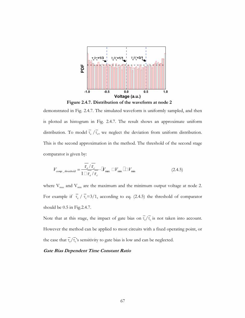
67
demonstrated in Fig. 2.4.7. The simulated waveform is uniformly sampled, and then
is plotted as histogram in Fig. 2.4.7. The result shows an approximate uniform
distribution. To model τe /τc, we neglect the deviation from uniform distribution.
This is the second approximation in the method. The threshold of the second stage
comparator is given by:
� � minminmax_ /1/ VVVV
ce
cethresholdcomp ���
��
����
(2.4.5)
where Vmax and Vmin are the maximum and the minimum output voltage at node 2.
For example if τe / τc=3/1, according to eq. (2.4.5) the threshold of comparator
should be 0.5 in Fig.2.4.7.
Note that at this stage, the impact of gate bias on τe/τc is not taken into account.
However the method can be applied to most circuits with a fixed operating point, or
the case that τe/τc’s sensitivity to gate bias is low and can be neglected.
Gate Bias Dependent Time Constant Ratio
-1.0 -0.5 0.0 0.5 1.0
Voltage (a.u.)
�e/�c=1/3 �e/�c=1/1 �e/�c=3/1
Figure 2.4.7. Distribution of the waveform at node 2

68
RTN time constant ratio not only depends on the trap itself but also depends on the
gate bias of the transistor. In researches people find that the time constant ratio
exponentially depends on the gate voltage [5][68][70]. To model this phenomenon a
sub-circuit structure is proposed in fig. 2.4.8(a). In fig. 2.4.8(a) a voltage controlled
voltage source (VCVS) is introduced to detect the gate voltage change in time
domain. By using the expression in circuit simulator (HSPICE), the exponential
gate V1=f(gate) (exp function)
Figure 2.4.8(a). VCVS to incorporate gate bias dependence.
0.00 0.02 0.04 0.06 0.08 0.100.2
0.4
0.6
0.8
1.0
0.00 0.02 0.04 0.06 0.08 0.10
Gat
e Vo
ltage
(V)
Time (s)
RTN
(a.u
.)
Time (s)
Figure 2.4.8(b). An example of RTN under sinusoidal gate voltage.

69
dependence is incorporated in the sub-circuit to generate RTN. Figure 2.4.8(b) is a
RTN waveform under a sinusoidal signal at gate. In the figure we see that the time
constant ratio clearly changes with the gate bias.
To test the impact of gate bias dependence on RO, the following structure in fig.
2.4.9 is proposed in experiments. In the structure, suppose the p/n ratio is β. Then
we tune the p/n ratio of all the even stages (red) to kβ, and the p/n ratio of all the
odd stages (blue) to β/k. Subsequently the period of high level is:
dhtkn+ �
��
� �11 (2.4.6)
And the period of low level is:
� �� � dltkn+ 11 � (2.4.7)
where n is the number of total stages, tdh, tdl are high level per stage delay and low
level per stage delay respectively. So the high-to-low period ratio is given below:
� � dl
dh
tt
kn+kn+
=γ ��
�
11
11 (2.4.8)
thus the duty cycle is expressed as the following:
1
CycleDuty +γγ
� (2.4.9)
With such a structure, we then add RTN to one of the NMOS in the first stage. The
experiments are under duty cycle of 20% and 80%, so the effective gate bias are
different and should result in different time constant ratio. The results are

70
demonstrated in fig. 2.4.10 and we can see that the phase noise spectrum has two
peaks with different values.
RTN Magnitude Modeling
In time domain the magnitude of RTN is modeled by assigning δV as the two levels
difference of the second stage comparator. The δV can also be extracted from PSD.
The PSD of RTN is expressed as [69]:
� �20
20
2
2114)(
������
fVfS
ecRTN ��
� (2.4.10)
Assume the given PSD is
� �20
0 211)(
��fSfS
��� (2.4.11)
Figure 2.4.9. Test RO structure with non-symmetrical duty cycle.
8.0M 12.0M 16.0M 20.0M 24.0M1E-14
1E-13
1E-12
1E-11
1E-10
1E-9
1E-8
1E-7
PSD
(V2 /H
z)
Frequency (Hz)
�e/�c=1/4
8.0M 12.0M 16.0M 20.0M 24.0M1E-14
1E-13
1E-12
1E-11
1E-10
1E-9
1E-8
1E-7
PSD
(V2 /H
z)
Frequency (Hz)
�e/�c=4/1
Figure 2.4.10. PSD of RO under different duty cycle.
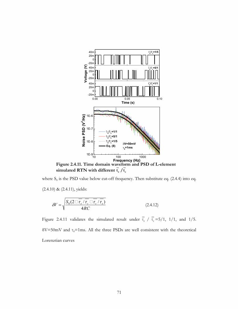
71
where S0 is the PSD value below cut-off frequency. Then substitute eq. (2.4.4) into eq.
(2.4.10) & (2.4.11), yields:
RCSV ecce
4)//2(0 ����
���
� (2.4.12)
Figure 2.4.11 validates the simulated result under τe / τc =5/1, 1/1, and 1/5.
δV=50mV and τ0=1ms. All the three PSDs are well consistent with the theoretical
Lorenztian curves
10 100 10001E-9
1E-8
1E-7
1E-6
Noi
se P
SD (V
2 /Hz)
Frequency (Hz)
�e/�c=1/1 �e/�c=5/1 �e/�c=1/5 Eq. (8)
�V=50mV�0=1ms
0.00 0.05 0.10-20m
020m40m
-20m0
20m40m
-20m0
20m40m
Time (s)
Volta
ge (V
)�e/�c=1/1
�e/�c=5/1
�e/�c=1/5
Figure 2.4.11. Time domain waveform and PSD of L-element
simulated RTN with different τe /τc

72
2.4.4 Design Benchmarks
This section studies the impact of RTN on SRAM and Ring Oscillator by using the
proposed L-shaped circuit. The differences between L-shaped circuit and traditional
RC unit are also investigated for the benchmark circuits.
Impact on SRAM
SRAM design is strongly constrained by size requirement so the transistors in the cell
can be ultra small, leading to huge RTN. Figure 2.4.1(c) is an example illustrating the
impact on SRAM. The simulated SRAM cell is based on 32nm Predictive
Technology Model [16]. The width to length ratio (W/L) of drive transistors and
load transistors are both 1/1, and the cell ratio is 1.2. An L-shaped circuit based
RTN generation block is adopted in one of the drive transistors. The magnitude of
RTN is 70mV, τ0=1ms, and τe /τc=1. To simplify the case, we assume that the trap is
close to the Si-SiO2 interface, such that the impact of gate bias on τe /τc can be
ignored [69]. In the simulation 100000 reads operations are performed in 1s, and the
failure times are recorded as nfailure. To compare the L-shaped circuit method with
traditional method, a white noise-RC unit noise source with the same PSD is also
simulated. The failure probabilities of SRAM cell are calculated by nfailure / 100000,
and are plotted in Fig. 2.4.1(c). From Fig. 2.4.1(c) first we see that different from the
continuous change of failure probability by traditional method, the RTN simulated
by L-shaped circuit shows a two-step shape. Moreover, the read failure probability is
a function of τe /τc. For example in Fig. 2.4.1(c) the mid level of simulated result with
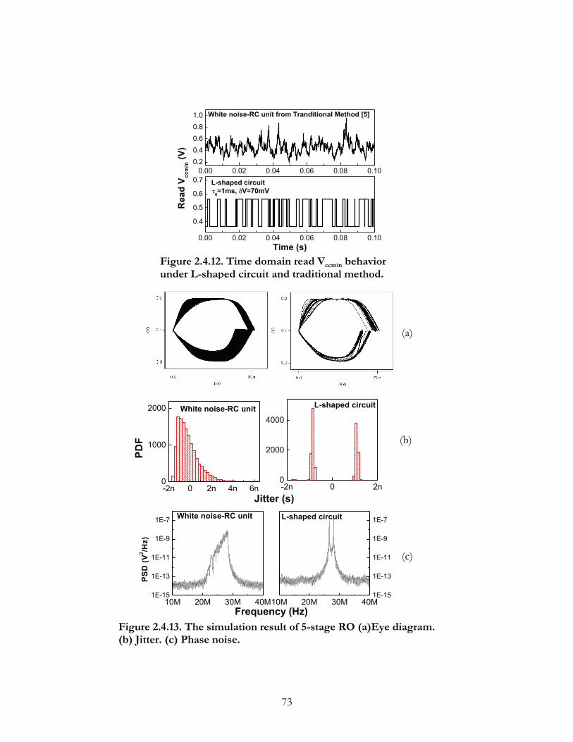
73
Figure 2.4.12. Time domain read Vccmin behavior
under L-shaped circuit and traditional method.
0.00 0.02 0.04 0.06 0.08 0.10
0.4
0.5
0.6
0.7
Time (s)
0.00 0.02 0.04 0.06 0.08 0.100.20.40.60.81.0
L-shaped circuit
Rea
d V
ccm
in (V
)�0=1ms, �V=70mV
White noise-RC unit from Tranditional Method [5]
-2n 0 2n0
2000
4000
Jitter (s)
L-shaped circuit
-2n 0 2n 4n 6n0
1000
2000
White noise-RC unit
10M 20M 30M 40M1E-15
1E-13
1E-11
1E-9
1E-7
PSD
(V2 /H
z)
White noise-RC unit
10M 20M 30M 40M1E-15
1E-13
1E-11
1E-9
1E-7
Frequency (Hz)
L-shaped circuit
Figure 2.4.13. The simulation result of 5-stage RO (a)Eye diagram.
(b) Jitter. (c) Phase noise.
(a)
(b)
(c)

74
and for τe /τc=3, 1/(1+τe /τc)=25%. The simulation results well validate this.
Besides the read failure probability, read Vccmin is also a very sensitive parameter to
RTN. In the simulation, we first sample the threshold voltage shift due to RTN at a
specific time point, and then Vccmin is detected by sweeping Vcc under the sampled Vth
shift. Figure 2.4.12 demonstrates the simulated read Vccmin vs. time of the 32nm
SRAM design under L-shaped circuit and traditional method. ~200mV shift due to a
70mV RTN is observed. Also with traditional method a prediction error arise as the
plot shows.
Impact on Ring Oscillator (RO)
The simulations of 5-stage RO with 4 fan-outs at each stage are performed in this
section. The RO is a low power example under Vdd=0.2V. The simulated RO is
based on 22nm PTM [16]. RTN is with τe /τc=1, τ0=10us, and δV=50mV. The width
of NMOS and PMOS are 15nm and 30nm respectively. The nominal frequency of
this RO is 27.36 MHz (T = 36.55ns).
To compare the differences between L-shaped circuit and traditional method, both
cases are studied. The simulation results are presented in Fig. 2.4.13. Figure 2.4.13(a)
is the eye diagram under different simulation method. We clearly see a discrete
waveform in L-shaped circuit simulated result from Fig. 2.4.13(a), whereas this is not
observed in traditional method simulated result. The differences between the two
methods are also presented in Fig. 2.4.13(b) of jitter distribution and Fig. 42(c) of
phase noise. The jitter distribution should be discrete because the discrete level of
75
RTN gives discrete operation point of RO, which is mis-predicted by traditional
method as Fig. 2.4.13 (b) shows. The jitter variation range is ~5% predicted by L-
shaped circuit, while the range simulated by white noise-RC unit is ~16%. The phase
noises under two methods are also different. L-shaped circuit simulated result with
RTN contributes two peak values near the nominal frequency as demonstrated in Fig.
2.4.13(c).
2.4.5 Summary
In this work a new method is proposed to meet the needs of time domain RTN
simulation for digital circuits with scaled CMOS technology. The method can
correctly reproduce RTN waveform, and is comprehensively validated in both
frequency and time domain. Assisted by the new method, the impacts of RTN on
SRAM and low power RO are studied, and the advantages compared to traditional
noise simulation are investigated.

76
Chapter 3 VARIABILITY ANALYSIS UNDER LAYOUT DEPENDENT
RAPID THERMAL ANNEALING PROCESS
3.1 Introduction
The aggressive scaling of CMOS devices significantly improves the performance, but
also leads to many undesirable effects. One of the most profound impacts is short-
channel effects, such as Drain Induced Barrier Lowering (DIBL) that sharply reduces
threshold voltage at shorter channel length and leads to a dramatic increase in the
leakage. To mitigate short-channel effects in scaled CMOS devices, advanced
fabrication technology has to adopt rapid-thermal annealing (RTA) process in order
to achieve ultra-shallow junction in the source/drain region. Different from
traditional thermal annealing, the RTA process applies a much shorter pulse (e.g.,
Lamp RTA [71] or Laser Annealing [73][75]) to heat the silicon substrate to a much
higher temperature (e.g., 4ms annealing at 1250oC) [72], such that dopants in the
source/drain and gate regions receive sufficient energy to be activated, but only have
the minimal period of time for the diffusion.
The RTA process is a must for nanoscale CMOS fabrication, achieving ultra-shallow
junction depth and low source/drain/gate resistance. On the other hand, one
distinct property of RTA is that the entire silicon substrate does not reach thermal
equilibrium due to the extremely short heating period. During this period, the exact
amount of energy and thus, the annealing temperature, depends on the reflectivity of
the silicon substrate: the reflectivity of the gate is usually lower than that of the
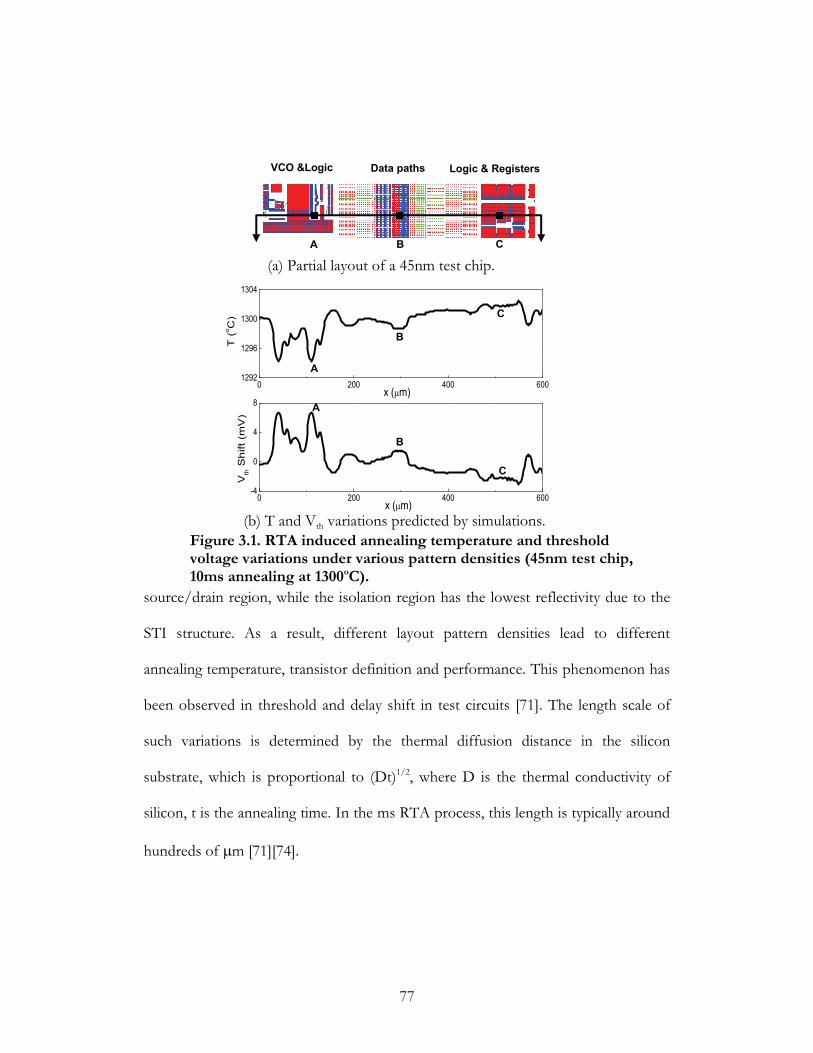
77
source/drain region, while the isolation region has the lowest reflectivity due to the
STI structure. As a result, different layout pattern densities lead to different
annealing temperature, transistor definition and performance. This phenomenon has
been observed in threshold and delay shift in test circuits [71]. The length scale of
such variations is determined by the thermal diffusion distance in the silicon
substrate, which is proportional to (Dt)1/2, where D is the thermal conductivity of
silicon, t is the annealing time. In the ms RTA process, this length is typically around
hundreds of �m [71][74].
Figure 3.1. RTA induced annealing temperature and threshold voltage variations under various pattern densities (45nm test chip,
10ms annealing at 1300oC).
B
A
C
(a) Partial layout of a 45nm test chip.
VCO &Logic Data paths
A B C
(b) T and Vth variations predicted by simulations.
Logic & Registers
B
A
C
0 200 400 6001292
1296
1300
1304
0 200 400 600-4
0
4
8
T (
oC
)
x (�m)
Vth S
hift
(m
V)
x (�m)
78
With such a thermal diffusion length, different silicon regions will have their own
annealing temperatures, depending on local layout pattern. The fluctuation in T
significantly affects transistor performance, such as Ion/Ioff ratio and Vth [73][75][76].
As an example, Fig. 3.1 illustrates the layout of a realistic 45nm test chip. Due to the
layout style, various components have a pronounced difference in pattern density
(Fig. 3.1a). With the proposed thermal simulation tool, Fig. 3.1b illustrates the
fluctuation in the annealing temperature, which directly induces Vth variation by
more than 30mV. The largest difference is observed close to the boundary of
different components, such Points A and C, where the non-uniformity of circuit
layout reaches the maximum.
To minimize the variations, improvements in both process technology and physical
design are necessary. In this work we develop a set of simulation and modeling
capability, as shown in Fig. 3.2, to bridge the understanding of the underlying physics
and circuit analysis under RTA, including (1) Transient thermal simulation to predict
the dependence of the annealing temperature on layout pattern density; (2) Process
simulation and modeling to analyze the primary impacts on equivalent gate oxide
thickness and effective channel length; and (3) Device simulation and compact
models to predict the change of device and circuit performance.
Using thermal simulation codes, we first obtain an appropriate simulation window to
define the pattern density. This helps us efficiently track the temperature profile in a
large scale layout. Then we investigate two independent variation mechanisms under

79
RTA, i.e., dopant activation and lateral source/drain diffusion. These two effects
further influence several important device parameters, including EOT, Vth, and Leff.
Based on TCAD simulation, we propose a set of analytical models that directly
predict these parameter changes from RTA conditions and PD. The new models will
enable efficient layout optimization in order to reduce the systematic variation due to
RTA.
We systematically validate the method with TCAD tools and published silicon data
under various conditions, including different annealing time, annealing temperature,
and doping in devices. This part is organized as follows: Section 3.2 presents the
theoretical background and the development of thermal simulation capability. It
defines an appropriate window size to extract pattern density under different RTA
conditions. Section 3.3 integrates process and device simulations to analyze dopant
activation lateral junction diffusion. Base on TCAD simulation results, we further
develop compact models to predict the change of threshold voltage and other device
Figure 3.2. The flow of joint thermal/TCAD simulation and compact modeling to investigate the RTA process.
RTA Simulation (Code developed)
Activated Dopant Concentration (Nact)
Device Simulation (Medici)
Pattern Dependent Annealing Temperature
Threshold Voltage (Vth), Gate Resistance (Rs) and IV Characteristics
Equivalent Gate Oxide Thickness
(EOT)
Process Simulation (Tsuprem4)
Effective Channel Length (Leff)
TCAD Simulation Compact Modeling

80
parameters. Finally we apply the new models to benchmark the variability of circuit
delay and leakage due to pattern-dependent RTA at 45nm node.
3.2 Thermal Simulation of Pattern Dependent RTA Process
In this section, we present the theoretical background and the code development of
RTA thermal simulation. The study is performed with a representative 45nm
technology. We use the equivalent emissivity in our thermal simulation in order to
simplify the simulation. To further improve the simulation efficiency, we study the
maximum window size that can be used to define local pattern density, as well as its
dependence on RTA conditions.
Thermal Simulation
In a typical RTA process, the energy source, such as the lamp or laser, emits energy
to the surface of the substrate. On the chip surface, different structures, e.g., gate,
source/drain, and STI, have different emissivity [75][76] and thus, they absorb
Figure 3.3. Layout thermal simulation. (a) simulation structure; (b) power profile in the experiment.
(a) (b)
Energy beam
0.0
0.2
0.4
0.6
0.8
1.0
Nor
mal
ized
Pow
er
Annealing Time Emissivity~0.43
Emissivity~0.5
Experiment Setup: Effective Annealing Time (teff): 1ms~1s Preheat Temperature: 650oC Peak Surface Temperature (T): 1250oC~1300oC
Si Substrate
Gate

81
different amount of energy during the annealing. This is the origin that induces non-
uniform temperatures within a die.
In order to investigate the interaction between pattern density and the annealing
temperature, we develop transient thermal simulation on the cross section of the
chip. Figure 3.3a illustrates the structure in thermal simulation. The initial condition
of the full wafer is usually at a constant preheat temperature, e.g., 650oC [71]. A
typical power profile of the annealing process is shown in Fig. 3.3b. Finite
Difference Method (FDM) is applied to solve the initial value problem (IVP). Such a
method is accurate, but not efficient enough if the chip size is large. To speed up the
simulation in mm scale, we introduce the concept of the equivalent emissivity for the
surface of the chip. The equivalent emissivity (�eq) is defined as the weighted average
of the emissivity of each layout pattern within a simulation window, depending on
the area density. The equivalent emissivity is given as the following:
� ���
��n
iwindowiieq AA
1�� (3.1)
where εi refers to the emissivity of a pattern, Ai is the area of the pattern in the
window, and Agrid is the total area of the simulation window. When the simulation
window is much smaller than the thermal diffusion distance, e.g. 1�m, a single value
of �eq is a sufficient representation of the thermal characteristics within the
simulation grid. For the vertical direction, since the active regions of study are much
thinner than the wafer thickness (usually around hundreds of μm), we treat the cross

82
section of wafer as a homogenous material. Overall, the process of radiation heating
based RTA has a much shorter ramp rate than traditional conduction based
annealing process. The entire chip area does not reach thermal equilibrium during
the annealing period [71].
Simulation Window Size
Using the newly developed thermal simulation tool, we are able to investigate the
thermal conduction and temperature distribution inside the substrate. However,
there is still a limitation on the window size we select to define the equivalent
emissivity (Eq. 3.1) and calculate the pattern density. The window size is preferred to
be large for fast simulation, but it should be small enough to track the change of the
temperature profile for an accurate performance prediction.
Figure 3.4. The search of the maximum window size during thermal simulation of the RTA process.
0 50 100 150 2001298
1300
1302
1304
1306
Window Size = 6�mTmax error~0.2oC
T (o C
)
X Direction (�m)
20ms RTA @ 1300oC
Window Size = 22.4�mTmax error~0.6oC

83
To identify the appropriate window size, we simulate a sample 45nm design with
various sizes of the simulation window. Within each window size, the emissivity of
different patterns is averaged to the equivalent emissivity. Figure 3.4 shows the
results from several representative window sizes using 20 ms RTA at 1300oC. The
maximum temperature error is defined as the maximum difference as compared to
the result from the minimum window size (100nm). Under a larger window size, the
components with higher spatial frequency are filtered out and therefore, the
simulation error increases. To guarantee sufficient accuracy in device performance
prediction, we define the threshold window size when the maximum T error reaches
0.6oC, which corresponds to 0.8mV Vth shift in this 45nm technology. In the sample
case, the appropriate window size is 22.4�m. The exact value depends on the RTA
conditions, such as the annealing time and T.
Figure 3.5 illustrates the window size dependence on annealing temperature and time
through thermal simulations. The criteria of post-annealing Vth shift is 1.1mV. The
Figure 3.5. Simulation window sizes under different RTA
conditions at 45nm node.
1250 1275 1300
20
30
40
50
Win
dow
Siz
e to
Def
ine
Equi
vale
nt E
mis
sivi
ty (�
m)
Annealing Temperature (oC)
10ms20ms40ms0.1s

84
window size can be approximated as a linear function of T. It is also proportional to
t1/2 due to the thermal diffusion process [77]. Therefore, we express the overall
dependence as:
� �� �22/1
121 BtBATALwindow ����� � (3.2)
where t refers to the annealing time, and A1, A2, B1, B2 are fitting parameters. Within
the simulation window, the pattern density and the equivalent emissivity are averaged
for fast thermal simulation, in order to predict the value of the annealing temperature
for further model calculations. Through this method, the simulation efficiency is
high enough to support chip-scale thermal simulations.
3.3 Compact Modeling of Performance Variability
There are two primary mechanisms that affect the threshold voltage in the RTA
process (Fig. 3.6). The first one is dopant activation in the gate. We propose compact
models to connect the annealing condition with dopant activation rate, equivalent
oxide thickness and threshold voltage. The second factor is effective channel length
defined by lateral thermal diffusion in the source/drain region. Due to the DIBL
effect, Vth is highly sensitive to the change of Leff. We describe the impact of the two
mechanisms in compact models and validate them against TCAD simulations and
published silicon data.
Dopant Activation
One major purpose of the RTA process is to electrically activate the dopants in the
gate and source/drain regions. Depending of the activation rate, the polysilicon gate

85
will have a finite doping level. When a suitable gate voltage is applied, it leads to the
depletion close to the interface between the gate and the dielectric. This depletion is
equivalent to the increase in oxide thickness and results in threshold voltage change.
The concept of equivalent oxide thickness (EOT) is usually used to describe the
phenomenon. The EOT is given as the following:
oxoxSipoly tWEOT ��� �� / (3.3)
Figure 3.7. Dopant activation rate depends on RTA conditions and is limited by solid solubility (2.2E20 at 1200oC and 1.4E20 at 1300oC).
1000 1200 1400 1600
6.0x10¹⁹
8.0x10¹⁹
1.0x10²⁰
1.2x10²⁰
1.4x10²⁰
10-5 10-3 10-1 1015.0x1019
1.0x10²⁰
1.5x10²⁰
2.0x10²⁰
2.5x10²⁰
Nac
t (cm
-3)
Tgate (oC)
Ngate=2E20 Ngate=3E20 Ngate=4E20
Solid SolublilityLimit above 1300oC: 1.4E20
Ngate=1E20 Ngate=1.5E20 Ngate=3E20 Model Fit
Solid Solubility Limit at 1200oC: 2.2E20
Nac
t (cm
-3)
Effective Annealing Time (s)
Figure 3.6. Two mechanisms affect device parameters in RTA process: dopant activation and lateral diffusion.
Dopant Activation and Poly-Depletion p y p
Lateral S/D Diffusion

86
where the Wpoly is the depletion width in polysilicon gate, tox is the gate oxide thickness,
εSi and εox are dielectric constant for silicon and oxide respectively. If tox is large
enough, the impact of poly-depletion can be ignored. However as technology scaling
continues, the oxide thickness is as thin as 1nm and thus, the variation in poly-
depletion can no longer be neglected.
In the RTA process, the dopants may not be completely activated due to the short
time, even though T is high. Therefore the depletion width, which is inversely
proportional to the square root of activated dopant concentration, becomes larger.
The increase in EOT further leads to larger Vth after the annealing.
Here we employ a simple model to connect the activated dopant concentration (Nact)
to the RTA process [78]:
�/maxminmax )( efftact eNNNN ����� (3.4)
1/
0
���� TkEae�� (3.5)
where Nmax refers to the maximum concentration of activated dopants; Nmin is the
minimum activated doping concentration, which refers to the activated doping
concentration before the annealing; τ refers to the activation time constant, which is
defined at the time that 50% dopants activated; teff is the effective annealing time such
that the activation rate is equivalent to that of the simulated temperature profile [78].
Their values are usually available from RTA process parameters. Figure 3.7 shows
the matching between analytical models and TCAD simulation results.

87
With active doping concentration, we are able to compute the change of EOT. In
order to achieve the same I-V characteristics, the electric field in the oxide-channel
surface should be constant, i.e., the electric field in the interface of the gate and the
dielectric is a constant. Since the electrical field is proportional to Wpoly�Nact, we
Figure 3.8. EOT has linear dependence on 1/Nact.
0.0 2.0x10⁻²⁰ 4.0x10-200.0
0.5
1.0
1.5
2.0
Tsuprem4 simulation Model
EO
T in
Pol
y-G
ate
(nm
)
1/Nact (cm3)
tpoly = a / Nact
Figure 3.9. The dependence of ∆Xj on the RTA process.
600 400 200 00
20
40
60
1200 1400 0
20
40
60
80
Junc
tion
Mov
e (n
m)
Annealing Time (ms)
Tgate=1250oC
Tgate=1300oC
Tsuprem4Model J
unct
ion
Mov
e (n
m)
Tgate (oC)
Dose=5E15 Dose=4E15 Dose=3E15
teff = 60ms

88
obtain Wpoly~1/Nact. We can express the EOT dependence as:
actoxpolyox NatttEOT /���� (3.6)
where a is a fitting parameter. Figure 3.8 validates the equation as compared to
TCAD simulations, which are extracted from the C-V characteristics [78]. By
integrating Eqs. 34-36, we are able to analytically predict the change of EOT from a
given RTA.
Effective Channel Length
A side effect of the annealing process is the lateral diffusion that changes the value of
effective channel length (Fig. 3.6). In RTA process the variation in temperature may
result in channel length variation in nm scale. Although the diffusion of source/drain
is relatively small and has a marginal impact on the junction depth, Leff, which has a
nominal value around 30nm at 45nm node, is very sensitive to the lateral junction
change. Even with the change of several nanometers, threshold voltage is
dramatically different, due to the exponential dependence of Leff through the DIBL
effect. We investigated the sensitivity of the junction change on annealing conditions
by performing Tsuprem4 conditions and extracting compact models, as shown in Fig.
3.9. As a characteristic of the diffusion process, the junction change is dependent on
(Dt)1/2, where D is the diffusion coefficient, and t is the annealing time. We apply a
polynomial equation to fit the dependence on the annealing temperature as the
following:
� � 0b
j TTaX ��� (3.7)

89
where ΔXj is the junction change after the annealing, T0 is a reference temperature
where the junction move is zero in a typical RTA process and a, b are a fitting
parameters.
The TCAD simulations further confirms that the junction change is relatively
insensitive to the doping level, as shown in the right figure in Fig. 3.9. Based on
Fick’s Law, the junction move has a square root dependence on the annealing time.
Extracted from our simulation, the dependence is described as:
00 )( DtttDX j ���� (3.8)
The parameter t0 is the equivalent time before RTA to account for the preheat and
other conditions, as well as to approximate the junction as an ideal abrupt shape for
model derivation. Fig. 3.9 evaluates the model with Tsuprem4 results under various
temperatures and the annealing time.
Figure 3.10. The shift of Vth due to RTA, as a compound of
changes in EOT and effect channel length.
23 24 25 26 27
200
300
400
500
30 25 20 15 10
200
300
400
500
EOT=2.0nm
|Vth
| (m
V)
EOT=1.2nm
EOT=2.8nm
Leff (nm)
|Vth
| (m
V)
EOT (A)
Leff=22.5nm Leff=24.5nm Leff=26.5nm
A typical 65nm MOS

90
Impact on Threshold Voltage
With the models of Leff and EOT variations, we further investigate the impact on
device parameter by performing device simulations. The typical variation of the RTA
annealing temperature in a 45nm design ranges from several oC to tens of oC. Such a
change results in the junction move within 2nm and the variation in Leff smaller than
4nm. In this small range of variations, the shift of Vth is approximately linear to Leff,
even though the DIBL effect is an exponential function of Leff. Figure 3.10 illustrates
the matching between models and TCAD simulations. Within the reasonable range
of EOT, we are also able to expand Vth as a linear function of EOT. We propose the
following model for the threshold dependence on Leff and EOT:
� � oxeffrefth tLBAVV ����� (3.9)
Thermal Annealing
Dopant Activation )/),(exp()(),( maxminmax �tTtNNNtTN effact �����
� �� �dttTTkEtt
aeff �� ���0
11 )('exp
S/D Lateral Diffusion (to define Leff) � �000 )()(),( DtttDTTatTX b
j ����� ),(2),(
0tTXLtTL jeffeff ����
Device Parameters
),(/),( tTNaTTTtTEOT actoxpolyox ���� � � ),(),(),( tTEOTtTLbaVtTV effrefth �����
TTtTVtTV thth ��!!�� /),(),(
Table 3.1. Compact models to predict Vth variation of a device under the RTA
process. T is predicted by thermal simulations with a given layout pattern.

91
where the A, B, Vref are fitting parameters.
Table II summarizes the entire set of models to calculate Vth variation from the
effective annealing temperature and time, which are predicted from thermal
simulation on a given layout with the appropriate window size. Based on these
results, a physical designer will be able to efficiently diagnose and optimize layout
pattern density to reduce performance variability. Figure 3.11 shows an example of
Vth variation induced by the RTA for a 65nm technology. As shown in Fig. 53, the
curve is not monotonic. This is because the threshold change is induced by both Leff
change and EOT change. While the Leff change is proportional to t1/2 and Tb, the
shift of EOT shift rate is only pronounced when the activation rate is larger than
50%, as shown in Fig. 3.7. Such differences lead to the behavior in Fig. 3.11 that is
well predicted by the new models.
1000 1100 1200 1300 1400
-4
-3
-2
-1
0
Model TCAD
Vth
Shi
ft (m
V/o C
)
Annealing Temperature (oC)
65nm Technology
10ms60ms240ms
Figure 3.11. The dependence of threshold shift on the annealing temperature and time.

92
Validation with Silicon Data
We implement the models in SPICE simulator and validate its prediction with
available published silicon data. Figure 3.12 shows the Vth shift vs. the sheet
resistance of the gate, which is an index of the activation rate in polysilicon [75]. The
silicon data are under different RTA annealing ramp rate, which is equivalent to
different effective annealing time (Eq. 3.4). Furthermore, we evaluate the newly
developed models the other set of 45nm silicon data. Figure 55 shows that at higher
annealing temperature, Ion/Ioff can be improved by ~10%, benefiting from higher
Figure 3.12. Compact models accurately predict the change of Vth and gate resistance under various RTA conditions.
Figure 3.13. Higher annealing temperature improves Ion/Ioff.
0 5 10 150
10
20
30
40
50
60
Model
T=1200oC
V th S
hift
(mV)
Gate Sheet Resistance (% delta)
Slowest Ramp Rate Intermediate Ramp Rate Highest Ramp Rate
teff=60msteff=73.2msteff=87.6ms
65nm Silicon [1](PMOS)
1.00 1.04 1.08 1.12 1.16 1.20
1.2
1.5
1.8 Model
I off (a
.u.)
Ion (a.u.)
45nm Silicon [2](NMOS)
1200oC
1020oC 1145oC

93
dopant activation rate and therefore, thinner poly-depletion thickness in EOT. In
both cases, our model well matches the published data using the same RTA
conditions.
3.4 Impact on Circuit Performance Variability
With the capabilities of compact modeling and circuit analysis, we benchmark the
change of circuit performance change under different layout pattern densities. The
Figure 3.14. Within-die variation of the leakage
at different sampling points in Fig. 43.
Figure 3.15. Within-die variation of RO frequency
in the 45nm design in Fig. 43.
0.8 0.9 1.0 1.1
50n
100n
150n
I off (A
/�m
)
Vdd (V)
Point C Point B Point A
20% shift
10ms RTA @ 1300oC (NMOS)
1301.7 oC1298.7 oC1294.5 oC
0.6 0.7 0.8 0.9 1.0-2.0
-1.5
-1.0
-0.5
0.0
0.5
1.0
RO
Fre
quen
cy (%
)
Vdd (V)
Point C Point B Point A
1301.7oC1298.7oC1294.5oC
10ms RTA @ 1300oC

94
patterns are taken from the 45nm layout as shown in Fig. 3.1. We simulate the
leakage current and the frequency of identical 11-stage ring oscillators at three
representative locations, Point A, B, and C in Fig. 3.1. Depending on their unique
pattern density, the annealing temperature is generated from thermal simulation and
used for model calculation of Vth shift. Other technology specifications are from
PTM 45nm technology [16]. Figs. 3.14 and 3.15 highlight the simulation results.
About 20% variation in the leakage and 3% variation in the frequency are observed
due to the non-uniformity in the layout. The leakage current becomes larger at the
position with higher emissivity and thus, lower T. Within the increasing tight budget
in power and timing, such an amount of variations need to be effectively reduced by
joint process and design efforts.
3.5 Summary
In this work, we develop the capabilities of thermal simulation and compact models
to analyze within-die variability due to pattern-dependent RTA process. The thermal
simulation tool predicts the annealing temperature from the layout pattern. The new
compact models further capture two major variations sources, EOT and Leff, during
the RTA, and calculate the shift of device parameters. The results are validated with
TCAD simulations and silicon data at 45nm and 65nm generations. They effectively
close the gap between the process knowledge and circuit simulation in order to
minimize transistor and circuit performance variability due to systematic RTA effects.

95
Chapter 4 CONCLUSION
In this work the intrinsic and manufacturing induced variations in CMOS are studied.
A SPICE based gate slicing method to simulate RDF and LER is presented. For
deeply scaled CMOS, an atomistic TCAD simulation is performed to study RDF,
LER, OTF and RTN all together. The compact models are proposed for those
variations, to predict the future trend. Moreover, the time domain simulation of
RTN is developed. In manufacturing induced variations, the Vth shift under layout
dependent RTA is studied. The change of effective oxide thickness and effective
channel length are finding to be the two main reasons account for the Vth variability.
Corresponding compact model suites are developed for future technology projection.
4.2 Future Work
4.2.1 Modeling and simulation of the interaction between RTN and NBTI
The compact model for RTN is an important future work. Traditional models follow
the theory that RTN is originated only from oxide traps, and the time constant is
dependent on the distance and the material of dielectric layer. While recent research
[81] indicates that interface traps may be another source of RTN. The traditional
models for RTN cannot give a correct prediction of the time constant then.
Moreover in recent research people find that RTN and NBTI are closely related [82].
Modeling and simulation on interaction between RTN and NBTI may help people to
fully understand the two phenomenons.
96
4.2.2 Deep understanding of RDF and LER induced statistical variability
In section 3 our study states that the Vth variation due to OTF will exceed the RDF
induced Vth variation. However this case happens under the assumption that people
keeps using Silicon dioxide as the material of dielectric layer. With the application of
high-k materials, the OTF induced variability is significantly suppressed. In the future
generations RDF and LER are still the main variation sources in CMOS. As device
scales continuous shrink, more additional effects come up, such as the non-Gaussian
Vth distribution [80], RDF induced mobility variations, and the Vth mismatch in
different operating region due to RDF. New efficient, flexible and reliable simulation
methods are desired. 2-D SPICE based slicing method may be a good candidate with
more improvement. New models are also needed for those effects with the support
from TCAD tools.

97
REFERENCES
[1] International Technology Roadmap for Semiconductors, 2008 (available at http://public.itrs.net).
[2] B. Hoeneisen and C. A. Mead, “Fundamental limitations in microelectronics—I. MOS technology,” Solid-State Electron., vol. 15, p. 819, 1972.
[3] K. Bernstein, et al., “High-performance CMOS variability in the 65-nm regime and beyond,” IBM J. Res. & Dev., vol. 50, no. 4/5, pp. 433-449, Jul./Sep., 2006.
[4] Hon-Sum Philip Wong, Yuan Taur, David J. Frank, Discrete random dopant distribution effects in nanometer-scale MOSFETs, Microelectronics and Reliability, Volume 38, Issue 9, September 1998, Pages 1447-1456
[5] N. Tega, et al., “Impact of threshold voltage fluctuation due to random telegraph noise on scaled SRAM,” Proc. IEEE IRPS, 2008, pp. 541-546.
[6] K. Sonoda, K. Ishikawa, T. Eimori, and O. Tsuchiya, “Discrete dopant effects on statistical variation of random telegraph signal magnitude,” IEEE TED, vol. 54, no. 8, pp. 1918-1925, Aug 2002.
[7] A. T. Putra, A. Nishida, S. Kamohara, and T. Hiramoto, “Random Vth variation indueced by gate edge fluctuations in nanoscale MOSFETs,” Silicon Nanoelectronics Workshop, pp. 73-74, 2007.
[8] S.M. Goodnick, D.K. Ferry, and C.W. Wilmsen, “Surface roughness at the Si(100)-SiO2 interface,” Physical Review B, vol. 32, no. 12, pp. 8171-8182, Dec, 1985.
[9] K. Takeuchi, “Channel size dependence of dopant-induced threshold voltage fluctuation,” Symp. VLSI Technology, pp. 72-73, 1998.
[10] Z. H. Liu, et al., “Threshold voltage model for deep-submicrometer MOSFETs,” Electron Devices, IEEE Transactions on, vol.40, no.1, pp.86-95, Jan 1993
[11] T. Ezaki, T. Ikezawa, A. Notsu, K. Tanaka, and M. Hane, “3D MOSFET simulation considering long-range coulomb potential effects for analyzing statistical dopant-induced fluctuations associated with atomistic process simulator,” Proc. SISPAD, 2002, pp. 91-94.
[12] Sentaurus User’s Manual, Synopsys, Inc., Mountain View, CA, v. 2009.6.

98
[13] G. Roy, F. Adamu-Lema, A.R. Brown, S. Roy, and A. Asenov, “Simulation of Combined Sources of Intrinsic Parameter Fluctuations in a ‘real’ 35nm MOSFET,” Proc. ESSDERC, 2005, pp. 337-340.
[14] S. Xiong, and J. Bokor, “Study of gate line edge roughness Effect in 50nm bulk MOSFET devices,” Proc. SPIE, Vol. 4689, 733 (2002)
[15] R. W. Keyes, “Physical limits in digital electronics,” Proc. IEEE, vol. 63, pp. 740–766, 1975.
[16] W. Zhao, Y. Cao, “New generation of predictive technology model for sub-45nm design exploration,” IEEE TED, vol. 53, no. 11, pp. 2816-2823, Nov. 2006. (Available at http://www.eas.asu.edu/~ptm)
[17] T. Hagivaga, K. Yamaguchi, and S. Asai, “Threshold voltage variation in very small MOS transistors due to local dopant fluctuations,” Symp. VLSI Technology, pp. 46–47, 1982.
[18] T. Mizuno, J. Okamura, and A. Toriumi, “Experimental study of threshold voltage fluctuation due to statistical variation of channel dopant number in MOSFETs,” IEEE Trans. Electron Devices, vol. 41, no. 11, pp. 2216–2221, Nov. 1994.
[19] T. Mizuno, “Influence of statistical spatial-nonuniformity of dopant atoms on threshold voltage in a system of many MOSFET’s,” Jpn. J. Appl. Phys., vol. 35, pp. 842–848, 1996.
[20] Y. Taur, et al., “CMOS scaling into the nanometer regime,” Proc. IEEE, vol. 85, no. 4, pp. 486–504, April 1997.
[21] V. K. De, X. Tang, and J. D. Meindl, “Random MOSFET parameter fluctuation limits to gigascale integration (GSI),” Symp. VLSI Technology, pp. 198–199, 1996.
[22] D. J. Frank, Y. Taur, M. Ieong, and H.-S. P. Wong, “Monte Carlo modeling of threshold variation due to dopant fluctuations,” Symp. VLSI Circuits, pp. 171-172, 1999.
[23] K. Takeuchi, T. Fukai, T. Tsunomura, A. T. Putra, A. Nishida, S. Kamohara, and T. Hiramoto, “Understanding random threshold voltage fluctuation by comparing multiple Fabs and technologies,” IEDM, pp. 467–470, 2007.
[24] A. Asenov, “Random dopant induced threshold voltage lowering and fluctuations in sub 0.1 micron MOSFETs: A 3D ‘atomistic’ simulation study,” IEEE Trans. Electron Devices, vol. 45, no. 12, pp. 2505–2513, Dec. 1998.

99
[25] A. Asenov, G. Slavcheva, A. R. Brown, J. H. Davies, and S. Saini, “Increase of the random dopant induced threshold fluctuations and lowering in sub-100 nm MOSFETs due to quantum effects: A 3-D density- gradient simulation study,” IEEE Trans. Electron Devices, vol. 48, no. 4, pp. 722–729, Apr. 2001.
[26] A. Asenov, A. R. Brown, J. H. Davies, S. Kaya, G. Slavcheva, “Simulation of intrinsic parameter fluctuations in decananometer and nanometer-scale MOSFETs,” IEEE Trans. Electron Devices, vol. 50, no. 9, pp. 1837-1852, Sep. 2003.
[27] Tsunomura, Takaaki; Nishida, Akio; Hiramoto, Toshiro, "Analysis of NMOS and PMOS Difference in V_{T} Variation With Large-Scale DMA-TEG," IEEE Transactions on Electron Devices, vol. 56, issue 9, pp. 2073-2080
[28] Takaaki Tsunomura, Fumiko Yano, Akio Nishida and Toshiro Hiramoto, "Possible Origins of Extra Threshold Voltage Variability in N-Type Field-Effect Transistors by Intentionally Changing Process Conditions and Using Takeuchi Plot," Jpn. J. Appl. Phys. 49 (2010) 074104
[29] T. Yamaguchi, H. Namatsu, M. Nagase, K. Yamazaki, and K. Kurihara, “Nanometer-scale linewidth fluctuations caused by polymer aggregates in resist films,” Appl. Phys. Lett., vol. 71, no. 16, pp. 2388-2390, 1997.
[30] T. Yamaguchi, H. Namatsu, M. Nagase, K. Kurihara and Y. Kawai, “Line-edge roughness characterized by polymer aggregates in photoresists,” Proc. SPIE, vol. 3678, no. 1, pp. 617-624, 1999.
[31] D. L. Goldfarb, et al., “Effect of thin-film imaging on line edge roughness transfer to underlayers during etch processes,” Journal of Vacuum Science & Technology B, vol. 22, no.2, pp. 647-653, 2004.
[32] H. Namatsu, M. Nagase, T. Yamaguchi, K. Yamazaki, K. Kurihara, “Influence of edge roughness in resist patterns on etched patterns,” Journal of Vacuum Science & Technology B, vol. 16, no. 6, pp.3315-3321, Nov. 1998.
[33] J. A. Croon, et al., “Line edge roughness: Characterization, mod-eling and impact on device behavior,” IEDM, pp. 307-310, 2002.
[34] S. Kaya, A. R. Brown, A. Asenov, D. Magot, and T. Linton, “Analysis of statistical fluctuations due to line edge roughness in sub 0.1 m MOSFETs,” Simulation of Semiconductor Processes and Devices, Springer, 2001.

100
[35] P. Oldiges, Q. Lin, K. Pertillo, M. Sanchez, M. Ieong, and M. Hargrove, “Modeling line edge roughness effects in sub 100 nm gate length devices,” SISPAD, pp. 131-134, 2000.
[36] S. Xiong and J. Bokor, “A simulation study of gate line edge roughness effects on doping profiles of short-channel mosfet de-vices,” IEEE Trans. Electron Devices, vol. 51, no. 2, pp. 228–232, Feb. 2004.
[37] S.-D. Kim, H. Wada, J. C. S. Woo, “TCAD-based statistical analysis and modeling of gate line-edge roughness effect on nanoscale MOS transistor performance and scaling.” IEEE TSM, vol. 17, no. 2, pp. 192-200, May 2004.
[38] B. Cheng, S. Roy, G. Roy, F. Adamu-Lema, A. Asenov, “Impact of intrinsic parameter fluctuations in decanano MOSFETs on yield and functionality of SRAM cells,” Elsevier Solid-State Electronics, vol. 49, pp. 740-746, 2005.
[39] Y. Nakagome, M. Horiguchi, T. Kawahara, and K. Itoh, “Review and future prospects of low-power RAM circuits,” IBM J. Res. & Dev., vol. 47, no. 5/6, pp. 525-552, Sep./Nov., 2006.
[40] Y. Ye, F. Liu, S. Nassif, Y. Cao, “Statistical modeling and simulation of threshold variation under dopant fluctuations and line-edge roughness,” DAC, pp. 900-905, 2008.
[41] C. Bencher, Y. Chen, H. Dai, W. Montgomery, and L. Huli, “22nm halfpitch patterning by CVD spacer self alignment double patterning (SADP),” Proc. of SPIE, vol. 6924, pp. 69244E.1-69244E.7, 2008.
[42] S. Sardo, et al., “Line edge roughness (LER) reduction strategy for SOI waveguides fabrication,” Microelectronic Engineering, vol. 85, no. 5-6, pp. 1210-1213. May-June 2008.
[43] Paul Zimmerman, “Double patterning lithography: double the trouble or double the fun?” SPIE Newsroom, 20 July 2009
[44] S.M. Goodnick, D.K. Ferry, and C.W. Wilmsen, “Surface roughness at the Si(100)-SiO2 interface,” Physical Review B, vol. 32, no. 12, pp. 8171-8182, Dec, 1985.
[45] Y. Ye, F. Liu, S. R. Nassif, M. Chen, Y. Cao, “Statistical Modeling and Simulation of Threshold Variation under Random Dopant Fluctuations and Line-Edge Roughness”
[46] Asenov, A.; Kaya, S., "Effect of oxide interface roughness on the threshold voltage fluctuations in decanano MOSFETs with ultrathin gate oxides," Simulation of

101
Semiconductor Processes and Devices, 2000. SISPAD 2000. 2000 International Conference on , vol., no., pp.135-138, 2000
[47] N. Tega, H. Miki, Z. Ren, C. P. D’Emic, Y. Zhu, D. J. Frank, J. Cai, M. A. Guillorn, D.-G. Park, W. Haensch and K. Torii, “Reduction of random telegraph noise in High-к / metal-gate stacks for 22 nm generation FETs,” IEDM, 2009.
[48] Y. Yuzhelevski, M. Yuzhelevski and G. Jung, “Random telegraph noise analysis in time domain,” Rev. Sci. Instrum. 71 (4) (2000) 1681–1688.
[49] L. Brusamarello, G. I. Wirth and R. da Silva, “Statistical RTS model for digital circuits, Microelectronics Reliability,” ESREF 2009, pp. 1064-1069.
[50] J. J. M. Pelgrom, A. C. J. Duinmaijer, A. P. G. Welbers, “Matching properties of MOS transistors,” IEEE JSSC, vol. 24, no. 5, pp. 1433-1440, Oct. 1989.
[51] K. Takeuchi, “Channel size dependence of dopant-induced threshold voltage fluctuation,” Symp. VLSI Technology, pp. 72-73, 1998.
[52] P. Gupta, A. Kahng, Y. Kim, S. Shah, D. Sylvester, “Modeling of non-uniform device geometries for post-lithography circuit analysis”, SPIE, vol. 6156, pp. 61560U.1-61560U.10, 2006.
[53] R. Singhal, A. Balijepalli, A. Subramaniam, F. Liu, S. Nassif, Y. Cao, “Modeling and analysis of non-rectangular gate for post-lithography circuit simulation,” DAC, pp. 823-828, 2007.
[54] W. J. Poppe, L. Capodieci, J. Wu, and A. Neureuther, “From poly line to transistor: building BSIM models for non- rectangular transistors,” Proc. SPIE, vol. 6156, pp. 235-243, 2006.
[55] Sentaurus Device User Guide, Version A-2008.09, Sep. 2008.
[56] S.-D. Kim, H. Wada, J. C. S. Woo, “TCAD-based statistical analysis and modeling of gate line-edge roughness effect on nanoscale MOS transistor performance and scaling.” IEEE TSM, vol. 17, no. 2, pp. 192-200, May 2004
[57] A. Subramaniam, R. Singal, Y. Cao, “Design rule optimization of regular layout for leakage reduction in nanoscale design,” ASP-DAC, pp. 474-479, 2008.
[58] J. Wu, J. Chen, K. Liu, “Transistor width dependence of LER degradation to CMOS device characteristics,” SISPAD, pp. 95-98, 2002.

102
[59] P. P. Naulleau, G.Gallatin, “Spatial scaling metrics of mask-induced line-edge roughness,” Journal of Vacuum Science & Technology B , vol. 26, no. 6, pp. 1903-1910, Nov. 2008.
[60] M. Chandhok, et al., “Improvement in linewidth roughness by postprocessing,” Journal of Vacuum Science & Technology B , vol. 26, no. 6, pp. 2265-2270, Nov. 2008.
[61] T. Jhaveri, et al., “Maximization of layout printability/manufacturability by extreme layout regularity,” J. Micro/Nanolitho., MEMS and MOEMS, vol. 6, no. 3, 031011, Jul.-Sep. 2007.
[62] C. Alexander, G. Roy, A. Asenov, “Random-dopant-induced drain current variation in nano-MOSFETs: A three-dimensional self-consistent Monte Carlo simulation study using “ab initio” ionized impurity scattering,” IEEE Trans. Electron Devices, vol. 55, no. 11, pp. 3251–3258, Nov. 2008.
[63] Verghese, N.; Allstot, D.J.; Masui, S.; , "Rapid simulation of substrate coupling effects in mixed-mode ICs ," Custom Integrated Circuits Conference, 1993., Proceedings of the IEEE 1993 , vol., no., pp.18.3.1-18.3.4, 9-12 May 1993
[64] T. Ezaki, T. Ikezawa, A. Notsu, K. Tanaka, and M. Hane, “3D MOSFET simulation considering long-range coulomb potential effects for analyzing statistical dopant-induced fluctuations associated with atomistic process simulator,” Proc. SISPAD, 2002, pp. 91-94.
[65] Jayaraman, R.; Sodini, C.G., "A 1/f noise technique to extract the oxide trap density near the conduction band edge of silicon," Electron Devices, IEEE Transactions on , vol.36, no.9, pp.1773-1782, Sep 1989
[66] T. H. Morshed, M. V. Dunga, J. Zhang, D. D. Lu, A. M. Niknejad and C. Hu, “Compact modeling of flicker noise variability in small size MOSFETs,” IEDM 2009.
[67] T.-H. Lee and G. Cho, “Monte Carlo based time-domain Hspice noise simulation for CSA-CRRC circuit,” Proceedings of the 10th SORMA XII 2003, pp. 328-333.
[68] J. P. Campbell, J. Qin, K. P. Cheung, L. C. Yu, J. S. Suehle, A. Qates, and K. Sheng, “Random telegraph noise in highly scaled nMOSFETs,” IRPS 2009, pp.382-388
[69] S.R. Li, W. McMahon, Y.-L.R. Lu, and Y.-H. Lee, "RTS Noise Characterization in Flash Cells," IEEE EDL , vol.29, no.1, pp.106-108, Jan. 2008

103
[70] N. Tega, “Study on Variability in Transistor Characteristics due to Random Telegraph Noise”, IEEE/ACM CVM 2009
[71] T. Gebel, L. Rebohle, R. Fendler, W. Hentsch, W. Skorupa, M. Voelskow, W. Anwand, R. A. Yankov, “Millisecond Annealing with Flashlamps: Tool and Process Challenges,” RTP, pp. 47-55, 2006.
[72] P. Timans, J. Gelpey, S. McCoy, W. Lerch, S. Paul, “Millisecond Annealing: Past, Present and Future,” Mater. Res. Soc. Symp. Proc. vol. 912, 2006.
[73] M. Bidaud, “High-Activation Laser Anneal Process for the 45nm CMOS Technology Platform,” RTP, pp. 251-256, 2007.
[74] T. Kubo, T. Sukegawa, E. Takii, T. Yamamoto, S. Satoh and M. Kase, “First Quantitative Observation of Local Temperature Fluctuation in Millisecond Annealing,” RTP, pp. 321-326, 2007.
[75] I. Ahsan, et al., “RTA-Driven Intra-Die Variations in Stage Delay, and Parametric Sensitivities for 65nm Technology,” VLSI Symposium on Technology, pp. 170-171, 2006.
[76] E. Granneman, X. Pages, H. Terhorst, K. Verheyden, K. Vanormelingen, E. Rosseel, “Pattern-Dependent Heating of 3D Structures,” Advanced Thermal Processing of Semiconductors, pp. 131-138, 2007.
[77] L. M. Feng, Y. Wang, D. A. Markle, “Minimizing Pattern Dependency in Millisecond Annealing,” International Workshop on Junction Technology, pp. 25-30, 2006.
[78] A. Mokhberi, P. B. Griffin, J. D. Plummer, E. Paton, S. McCoy, K. Elliott, “A Comparative Study of Dopant Activation in Boron, BF2, Arsenic, and Phosphorus Implanted Silicon,” IEEE TED, vol. 49, no. 7, pp. 1183-1191, July 2002.
[79] F. Ootsuka, “An Engineering Method to Extract Equivalent Oxide Thickness and its Extension to Channel Mobility Evaluation,” IEEE TED, vol. 49, no. 12, pp. 2345-2348, Dec. 2002.
[80] Reid, D.; Millar, C.; Roy, G.; Roy, S.; Asenov, A.; , "Statistical enhancement of combined simulations of RDD and LER variability: What can simulation of a 105 sample teach us?," Electron Devices Meeting (IEDM), 2009 IEEE International , vol., no., pp.1-4, 7-9 Dec. 2009
[81] Campbell, J.P.; Qin, J.; Cheungl, K.P.; Yu, L.; Suehlel, J.S.; Oates, A.; Sheng, K.; , "The Origins of Random Telegraph Noise in Highly Scaled SiON nMOSFETs," Integrated

104
Reliability Workshop Final Report, 2008. IRW 2008. IEEE International , vol., no., pp.105-109, 12-16 Oct. 2008.
[82] Tsukamoto, Y.; Seng Oon Toh; Changhwan Shin; Mairena, A.; Tsu-Jae King Liu; Nikolic, B.; , "Analysis of the relationship between random telegraph signal and negative bias temperature instability," Reliability Physics Symposium (IRPS), 2010 IEEE International , vol., no., pp.1117-1121, 2-6 May 2010.