modeling and simulation of high speed interconnects - ncsu coe people
TRANSCRIPT
MODELING AND SIMULATION OF HIGHSPEED INTERCONNECTS
by
BARIBRATA BISWAS
A dissertation submitted to the Graduate Faculty ofNorth Carolina State University
in partial fulfillment of therequirements for the Degree of
Master of Science
Department of Electrical and Computer Engineering
Raleigh, NC1998
APPROVED BY:
W. Liu P. D. Franzon
M. B. SteerChair of Advisory Committee

Abstract
BISWAS, BARIBRATA. Modeling and Simulation of High Speed Intercon-nects. (Under the direction of Michael B. Steer.)
A three dimensional interconnect modeling software (Layout2FastCap)was developed that takes a Layout (CIF) as its input and generates thecapacitance matrix using a multipole accelerated boundary element methodbased numerical solver (FastCap). The software incorporates a new techniquefor simulating the ground plane using image method. A flow (Single NetCapacitance Extraction) was developed to handle larger layouts than thatcan be handled by Layout2FastCap. Experimental characterizations of theinterconnects were also carried out. Results obtained from measurementswere compared with the simulation results. The software Layout2FastCap isavailable by sending email to [email protected].

Biographical Summary
Baribrata Biswas was born in Ichapur, India on June 16, 1974. He re-ceived his B. Tech. degree in Electrical Engineering at the Indian Institute ofTechnology, Kanpur, India in May 1995. While pursuing the B. Tech. degreehe worked as a summer intern at the National Center of Astrophysics, Pune,India (1993) and at the Indian Institute of Science, Bangalore, India (1994).From July 1995 to July 1996 he worked at Cadence Design Systems, Noida,India. He was admitted into the Masters Program at North Carolina StateUniversity in Fall 1996. While working towards his M. S. degree he held aCadence Design Systems’ Fellowship and a Research Assistantship with theElectronics Research Laboratory in the Department of Electrical and Com-puter Engineering. In the summer of 1997 he worked as an intern at CadenceDesign Systems, Cary, North Carolina. His research interests include inter-connect modeling and simulation, analog and digital circuit design and solidstate devices.

Acknowledgments
I wish to thank my advisor Dr. Michael Steer for his guidance and supportduring my graduate studies and Dr. Paul Franzon and Dr. Wentai Liufor serving on my committee. I thank Cadence Design Systems, Inc. forsponsoring the Cadence Design Systems’ Fellowship which supported mygraduate studies.
I like to recognize the assistance of my graduate student colleagues. FirstSteven Lipa and Westerfield Ficken for providing with the measurement data.Alan Glaser for his help to understand the layout of the test chip. CarlosChristoffersen for his help with the CIF parser. I also wish to thank otherpeople in my group, Mete Ozkar, Christofer Hicks, Huan-sheng Hwang andUsman A. Mughal who helped me in numerous other ways. Last, but not theleast, I wish to thank my friends Uday Mudoi and Somshubro Pal Chaudhuryfor their advice and help.

Contents
List of Figures v
List of Tables vii
1 Introduction 11.1 Motivation . . . . . . . . . . . . . . . . . . . . . . . . . . . . . 11.2 Thesis Overview . . . . . . . . . . . . . . . . . . . . . . . . . . 2
2 Literature Review 32.1 Introduction . . . . . . . . . . . . . . . . . . . . . . . . . . . . 32.2 Capacitance Extraction . . . . . . . . . . . . . . . . . . . . . . 42.3 FastCap . . . . . . . . . . . . . . . . . . . . . . . . . . . . . . 52.4 Through Line Deembedding Procedure . . . . . . . . . . . . . 6
3 Capacitance Extraction 83.1 Introduction . . . . . . . . . . . . . . . . . . . . . . . . . . . . 83.2 Layout . . . . . . . . . . . . . . . . . . . . . . . . . . . . . . . 103.3 Caltech Intermediate Format . . . . . . . . . . . . . . . . . . . 133.4 Layout2FastCap . . . . . . . . . . . . . . . . . . . . . . . . . . 13
3.4.1 CIF Parser . . . . . . . . . . . . . . . . . . . . . . . . 143.4.2 Rectangle Generator & Connectivity Extractor . . . . . 173.4.3 Three Dimensional Modeler . . . . . . . . . . . . . . . 223.4.4 Mesher . . . . . . . . . . . . . . . . . . . . . . . . . . . 233.4.5 Limitations of Layout2FastCap . . . . . . . . . . . . . 23
3.5 Modeling of Ground Plane . . . . . . . . . . . . . . . . . . . . 253.5.1 Assumptions . . . . . . . . . . . . . . . . . . . . . . . . 253.5.2 Image Method . . . . . . . . . . . . . . . . . . . . . . . 263.5.3 Single Conductor Over Ground Plane . . . . . . . . . . 273.5.4 Two Conductors Over Ground Plane . . . . . . . . . . 30
iv

3.5.5 Generalization of the solution . . . . . . . . . . . . . . 333.6 Interpretation of the Capacitance Matrix of the CMOS Inverter 343.7 Single Net Capacitance Extraction Flow . . . . . . . . . . . . 35
4 Experimental Results 394.1 Introduction . . . . . . . . . . . . . . . . . . . . . . . . . . . . 394.2 Measurement Methodology . . . . . . . . . . . . . . . . . . . . 394.3 Measurement Setup . . . . . . . . . . . . . . . . . . . . . . . . 414.4 Test Chip . . . . . . . . . . . . . . . . . . . . . . . . . . . . . 424.5 Comparison of Synthesized and Measured Open Circuit in the
Through Line Calibration Technique . . . . . . . . . . . . . . 424.5.1 Synthesis of Open Circuit Reflection Coefficient . . . . 424.5.2 Measurement of Open Circuit Reflection Coefficient . . 444.5.3 Comparison . . . . . . . . . . . . . . . . . . . . . . . . 45
4.6 Measurement Results . . . . . . . . . . . . . . . . . . . . . . . 454.6.1 Dimensional Measurement . . . . . . . . . . . . . . . . 484.6.2 S Parameters and Capacitance Measurements . . . . . 51
5 Conclusion 545.1 Conclusions . . . . . . . . . . . . . . . . . . . . . . . . . . . . 545.2 Future Research . . . . . . . . . . . . . . . . . . . . . . . . . . 55
A Caltech Intermediate Format 60A.1 Syntax . . . . . . . . . . . . . . . . . . . . . . . . . . . . . . . 60
B Layout2FastCap 63B.1 Input Files . . . . . . . . . . . . . . . . . . . . . . . . . . . . . 63
B.1.1 Process Data File . . . . . . . . . . . . . . . . . . . . . 64B.1.2 Layer Mapping File . . . . . . . . . . . . . . . . . . . . 64
B.2 Program Implementation . . . . . . . . . . . . . . . . . . . . . 65B.2.1 Source Files . . . . . . . . . . . . . . . . . . . . . . . . 65B.2.2 Makefile . . . . . . . . . . . . . . . . . . . . . . . . . . 66

List of Figures
3.1 Flow Diagram of Layout2FastCap. . . . . . . . . . . . . . . . 93.2 Layout of a CMOS Inverter. . . . . . . . . . . . . . . . . . . 103.3 Vertical Profile of a two layer metal and a single layer poly
process. The variables 1 to in this figure are explained inAppendix B. . . . . . . . . . . . . . . . . . . . . . . . . . . . 12
3.4 Extraction of routing layers from the layout of the CMOSinverter. . . . . . . . . . . . . . . . . . . . . . . . . . . . . . . 16
3.5 Conversion of a round flash to a square. . . . . . . . . . . . . 163.6 Conversion of a manhattan shaped polygon to rectangles. . . 173.7 Conversion of a wire to rectangles. . . . . . . . . . . . . . . . 183.8 Conversion of Polygon and Wires to rectangles for both metal1
and poly layer: (a) poly; and (b) metal1 . . . . . . . . . . . . 193.9 Generation of a new rectangle from two old rectangles in con-
tact layer that overlap each other. . . . . . . . . . . . . . . . 203.10 Rectangles in a typical interconnect layer. . . . . . . . . . . . 213.11 Discretized three dimensional view of the CMOS inverter: (a)
top view; and (b) bottom view. . . . . . . . . . . . . . . . . . 243.12 Illustration of Image Method: (a) a conductor over a ground
plane; and (b) equivalent configuration with the image of theconductor. . . . . . . . . . . . . . . . . . . . . . . . . . . . . 26
3.13 Two configurations used by FastCap to generate the 2 × 2capacitance matrix for a two body problem. . . . . . . . . . . 27
3.14 Conductor over ground and its equivalent Image Method for-mulation. . . . . . . . . . . . . . . . . . . . . . . . . . . . . . 29
3.15 Two conductors over the ground plane: (a) actual structure;and (b) equivalent Image Method formulation with four con-ductors. . . . . . . . . . . . . . . . . . . . . . . . . . . . . . . 30
3.16 Two conductors over the ground plane. . . . . . . . . . . . . 31
vi

3.17 The four configurations used by FastCap to solve the four bodyproblem. . . . . . . . . . . . . . . . . . . . . . . . . . . . . . 32
3.18 Conversion of a 2n × 2n capacitance matrix resulting fromapplication of the image method to an n × n capacitancematrix. . . . . . . . . . . . . . . . . . . . . . . . . . . . . . . 33
3.19 A section of a victim net with few of its surrounding nets. Thebox defines the region of influence. . . . . . . . . . . . . . . . 36
3.20 Artificial Boundary Charge Correction Scheme. . . . . . . . . 38
4.1 Set-up for microwave measurements : (a) Test set-up using aCascade Microtech probe station, picoprobes from GGB in-dustries and Hewlett Packard Automatic Network Analyzer(ANA) HP8510C. Illustration of Through Line (TL) calibra-tion procedure : (b) Through measurement (c) Line measure-ment. . . . . . . . . . . . . . . . . . . . . . . . . . . . . . . . 40
4.2 Through connection in the Through Line calibration proce-dure: (a) network connection; and (b) signal flow graph withmeasured fixture S parameters of the two port network. . . . 43
4.3 Signal flow graphs: (a) model of the through connection withidentical fixturing; and (b) ideal open circuit placed at fixtureport 2A. . . . . . . . . . . . . . . . . . . . . . . . . . . . . . . 44
4.4 Plan View and cross section view of an open circuit structure. 454.5 Magnitude comparison of measured and synthesized open cir-
cuit for metal1 layer. . . . . . . . . . . . . . . . . . . . . . . 464.6 Magnitude comparison of measured and synthesized open cir-
cuit for metal2 layer. . . . . . . . . . . . . . . . . . . . . . . 464.7 Magnitude comparison of measured and synthesized open cir-
cuit for metal3 layer. . . . . . . . . . . . . . . . . . . . . . . 474.8 Line diagram of a metal line (in metal1 layer). The TiTu
(titanium-tungsten) layer was deposited and then plated withaluminum. . . . . . . . . . . . . . . . . . . . . . . . . . . . . 47
4.9 Scanning Electron Micrograph of the cross-section of a line in(a) metal1; and (b) metal3 layers. . . . . . . . . . . . . . . . 49

List of Tables
4.1 Various Dimensions of the Test Structures. . . . . . . . . . . . 504.2 Various Measured and Simulated Parameters of the Test Struc-
tures. . . . . . . . . . . . . . . . . . . . . . . . . . . . . . . . . 524.3 Various Derived Parameters of the Test Structures. . . . . . . 53
viii

Chapter 1
Introduction
1.1 Motivation
As integrated circuit processing technology marches relentlessly down throughdeep submicron feature sizes, chip performance limitations, such as systemdelay and signal integrity, are coming to be determined more by intercon-nect effects than by active device characteristics [1]. Although, the deviceand wire dimensions are decreasing, the size of the chip is increasing. Thisimplies that the number of interconnects as well as their lengths are increas-ing with each new generation of advanced logic and memory chips. This iscontributing to significant parasitic loading.
Increasing the number of metal layers and changing the aspect ratio ofmetal lines reduces the effect of interconnect capacitance to a certain extent.The upper metal layers (sometimes called ecto layers) have lower capacitanceto the ground because of the shielding effect of lower metal layers (sometimescalled endo layers). Also, the lines in endo layers are narrower and taller i.e.,their vertical height is more than their horizontal width. With less width, thecapacitance to the ground is decreased, but there is an increase in resistancewhich is compensated by increasing the height (the vertical metal dimension).
Other than designing interconnects with lower parasitic loading, effortsare made to characterize them more accurately. Resistance is determinedby the geometry of the line only and does not change depending on thedistribution of the wires in its surroundings. Capacitance is strongly affectedby geometry and the distribution of nearby conductors.
1

CHAPTER 1. INTRODUCTION 2
1.2 Thesis Overview
This thesis describes efforts made to characterize the capacitance of on-chipinterconnects in deep submicron designs. Since, interconnects in high speeddesigns are considered, it is necessary to characterize the capacitance withhigh accuracy because this determines the accuracy of the RC-delay of an in-terconnect. Higher accuracy in the calculation of RC delay of an interconnectallows a designer to achieve higher performance.
Chapter 2 is a review of literature relevant to on-chip capacitance ex-traction methodologies. It describes the techniques of numerical modeling ofinterconnects and measurement procedures for experimental characterizationof interconnects. Chapter 3 describes a tool which facilitates the accurateextraction of interconnect capacitance. It introduces a novel concept of simu-lation of the ground plane. Chapter 4 describes the experimental proceduresand the results obtained from the experimental characterization of intercon-nects on a test chip. Chapter 5 presents conclusion derived from this projectand areas that need further exploration in the future.

Chapter 2
Literature Review
2.1 Introduction
With shrinking device sizes, increasing circuit density and improving tran-sistor performance with each new chip generation, the electrical performanceof on-chip wiring becomes increasingly significant. The growing importanceof VLSI on-chip interconnects has been recognized by the semiconductorindustry and the scientific research community, as indicated by the increas-ing volume of work presented in related conferences and journals [2] [3] [4][5]. The semiconductor industry has proposed significant improvements toULSI interconnect technology in the most recently issued National Technol-ogy Roadmap for Semiconductors [1].
The majority of the recent work can be divided into several categories.The first of these addresses chip fabrication and unit processes: for example,how to increase the number of wiring levels, decrease dimensions, improvereliability and yield, and/or reduce cost through novel tools or processes. [6]describes a process that includes reactive-ion-etched (RIE) aluminum-alloylines, tungsten interlevel studs and chemical-mechanical polishing (CMP) forglobal and local planarization of insulators and metal levels.
There is also a body of recent work devoted to developing new inter-connect materials, such as insulators with lower dielectric constants thanthe industry-standard SiO2 [7] and metals with lower resistivities than thestandard aluminum alloys. An example of this kind of work is reported in[8] which achieves multilevel integration of copper interconnects with a lowdielectric constant polymide.
A third recently emphasized category for VLSI interconnect investigation
3

CHAPTER 2. LITERATURE REVIEW 4
comprises electrical performance modeling and measurements, and examina-tion of the effect of interconnect parasitics on circuits and systems. Refer-ences [4] and [5] contains an extensive and thorough development of suchissues.
This thesis addresses issues related to capacitance extraction of intercon-nects using numerical methods and measurement of interconnect capacitance.In this chapter some background related to these is provided.
2.2 Capacitance Extraction
In the design of very high performance circuits, it is important to know thedelay contributed by the interconnection network. With the present technol-ogy the delay in the interconnection line is because of the resistance and thecapacitance of the line. Calculation of the resistance of an interconnect iseasier than that of the capacitance of an interconnects because the resistanceof an interconnect does not depend on its surroundings. On the other hand,capacitance of an interconnect depends on the surrounding conductors andtheir geometry.
The commercial extraction tools take the approach of rule-based evalua-tion. The commercial tools generally tune themselves to the full field solutionof a bunch of small test structures and generate a look up table. However,they ultimately incur large errors due to their necessity to partition any prob-lem domain into very small pieces and then to reassemble the results applyingthe rules to those several small pieces. In [9] a hierarchical two-dimensionalfield solution technique is suggested for interconnect capacitance extraction.This has higher accuracy than rule-based extractors without losing muchefficiency.
Various numerical techniques have been developed for accurate capaci-tance extraction. They fall into the following three categories: (1) the Finite-Difference Method (FDM) [10], (2) the Finite-Element Method (FEM) [11]and (3) the Boundary-Element Method (BEM) [12, 13, 14, 15, 16]. In [17]these three methods have been compared and it was found that BEM basedmethods are the best for interconnect capacitance extraction.
In both the FDM and the FEM, the external field is discretized. Thisfield, in principle, extends to infinity and can not be truncated easily and sothis leads to a very large matrix to be solved. Although the matrix is sparse,often exhaustive computational resources (time and memory) are required.Spatial solvers [18] only partially alleviate these problems. Alternatively,

CHAPTER 2. LITERATURE REVIEW 5
a technique called Geometry Independent Measured Equation of Invariance(GIMEI) [19] can be used to achieve a much smaller sparse matrix.
On the other hand, in the BEM, only the boundary of the field region isdiscretized. Hence, the 3D problem is effectively reduced to a 2D problem.The resulting matrix is therefore much smaller, but full. Boundary elementmethods are most effective when the medium is regular or in the capacitanceextraction case when the chips have a stratified dielectric structure. To acertain extent, this is usually the case because of planarization.
The BEM matrix must be inverted and without special techniques, thiswould result in O(N3) time complexity, where N is a measure of the size ofthe layout. In [20] a multipole accelerated boundary-element method tech-nique is presented that circumvents the above problem. In this technique,to compute the matrix elements, an elementary solution of the partial differ-ential solution (first order Green’s function) is integrated over each possiblepair of boundary elements. The multipole method hierarchically clustersboundary elements in order to approximate the mutual influence betweenfar away pairs. The clustering also helps with the matrix inversion and asa result the computational complexity is reduced to O(Nm) where m is thenumber of different conductors and N is a measure of the size of the layout.A faster and general version of this algorithm is presented in [21]. A programnamed FastCap [22] was developed which implements this algorithm. In thenext section, the basic concepts of FastCap are discussed. A commercial toolRaphael [23] exists that can use either FEM or BEM to extract interconnectcapacitance.
2.3 FastCap
FastCap is a multipole accelerated boundary-element method based programthat calculates the capacitance between arbitrary shaped conductors in auniform dielectric medium. The algorithm used here is an acceleration ofthe boundary-element technique (as discussed in the previous section) forsolving the integral equation associated with the multiconductor capacitanceextraction problem.
The usual approach to solve Laplace’s equation for three-dimensional ca-pacitance calculations is to apply boundary element technique to the integralform of Laplace’s equation [15] [16]. Consider a system of m ideal conductorsembedded in a uniform lossless dielectric medium. The capacitance of sucha system can then be summarized by an m×m symmetric matrix C , where

CHAPTER 2. LITERATURE REVIEW 6
the j-th column of C has a positive entry Cjj , representing the self capaci-tance of conductor j, and negative entries Cij representing coupling betweenconductors j and i, i = 1, 2, ... m, i 6= j. To determine the j-th columnfor the capacitance matrix, one need to solve for the surface charges on eachconductor produced by raising conductor j to one volt while grounding therest. Then Cij is numerically equal to the charge on conductor i, i = 1,2, ... m. Repeating this procedure m times gives the m columns of C .
In this approach the surfaces or edges of all the conductors are brokeninto small panels and it is assumed that on each panel i, a charge, qi, isuniformly or piecewise linearly distributed. With the known conductor po-tential, FastCap finds the charge qi on each panel. The total charge on agiven conductor is then found by summing up the charges on each panel ofthe conductor. This total charge is the total capacitance of the conductorbecause there is a unit potential difference between the conductors.
FastCap is limited to very simple structures. Complex structures mustbe partitioned by hand and the panels have to be generated manually.
2.4 Through Line Deembedding Procedure
Experimental characterization of interconnect capacitance is generally doneby measuring the capacitances of test structures on a chip. A lot of differentmeasurement techniques are described in the literature [28, 29, 31, 32].
In [29, 30] an area efficient measurement technique was used. It is basedon the through-line (TL) deembedding procedure. In this section the de-tails of through-line deembedding procedure will be discussed and will becompared with the through-reflect-line (TRL) deembedding procedure.
The through-line deembedding procedure is presented in [27]. TL uti-lizes measurements of two lengths of line following approximate open-short-line calibration. TL accounts for the frequency dependent characteristicimpedance of the line and avoids the periodic glitches inherent to the TRLprocedure. TRL related methods of calibration are the most accepted tech-niques for deembedding fixtures in planar microwave measurement systems[33]. TRL has two major shortcomings.
1. The measurement uncertainties that result when the phase delay alongthe line is an integer n × 360o ± 20o resulting in glitches in the deem-beded response of the device under test. These periodic glitches arelargely due to the arbitrary reflection standard. The phase uncertainty

CHAPTER 2. LITERATURE REVIEW 7
is largely removed if the reflection standard is known precisely or oth-erwise removed from TRL calibration.
2. The accuracy depends predominantly on the estimate of the character-istic impedance, ZC , of the line. Estimation of ZC is usually made usingTDR measurements or through careful design of a transmission line tominimize reflection so that ZC approximates the system measurementimpedance Zref .
Through-line deembedding procedure solves the above two problems. Itis implemented in the following three steps.
1. Open-short-load (OSL) calibration is applied to each of the two testports. The OSL calibration need not be precise, the only requirementis that the same reference impedances be presented to the two ports.
2. Through and line measurements are then performed. Because of thesymmetry the through measurement yields the reflection coefficient ofan ideal short or open placed at the fixture reference plane. This elim-inates the need of using an arbitrary reference in the TRL calibrationalgorithm thus removing the major source of phase ambiguity.
3. The frequency dependent characteristic impedance of the line is thendetermined.
The first two steps denote a two-tier calibration procedure. Following theabove three steps yield precise in-situ calibration. Furthermore the glitchesassociated with TRL deembedding are largely eliminated and this is achievedby implementing steps 1 and 2 alone.
Chapter 3
Capacitance Extraction
3.1 Introduction
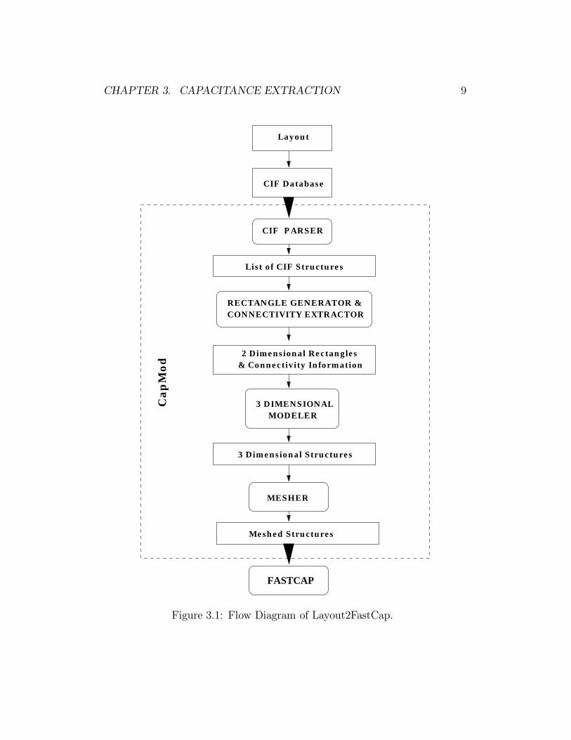
This chapter describes the tool that was developed to model on-chip inter-connects for accurate capacitance extraction. The tool uses as it core enginea boundary element based numerical solver called FastCap (see literaturereview in Chapter 2). As pointed out before it is quite difficult to calculatethe capacitance of a group of arbitrary shaped conductors using FastCap.FastCap does not have a preprocessor that can model arbitrary shaped con-ductors and generate the input files for it. So, a tool was developed for thispurpose and named Layout2FastCap (Conversion of a Layout to FastCapinput format). It provides a frontend for FastCap that makes it possible toextract interconnect capacitance of any arbitrary design.
Layout2FastCap takes as its input a layout stored in Caltech Intermedi-ate Format (CIF) (see Appendix A for details about this format). From theCIF file it extracts the interconnects, generates three dimensional structuresfor all the interconnects, discretizes the surfaces of these three dimensionalstructures and generates files containing panels (see Figure 3.1). Panels arerectangular or triangular in shape and are generated by dividing the sur-faces of the three dimensional interconnects into small parts. Panels arerepresented by the coordinates of their corners. FastCap parses these filescontaining panels and uses boundary element techniques to determine thecapacitance matrix for the system.
Layout2FastCap can handle a small layout with around a dozen intercon-nects. The size of the layout that can be 1 by Layout2FastCap is limitedby the size of the RAM of the computer that is used for executing FastCap.
8
CHAPTER 3. CAPACITANCE EXTRACTION 9
CIF Database
CIF PARSER
FASTCAP
Meshed Structures
Layout
Cap
Mod
List of CIF Structures
& Connectivity Information2 Dimensional Rectangles
MESHER
3 Dimensional Structures
MODELER3 DIMENSIONAL
RECTANGLE GENERATOR & CONNECTIVITY EXTRACTOR
Figure 3.1: Flow Diagram of Layout2FastCap.
CHAPTER 3. CAPACITANCE EXTRACTION 10
This is because with a larger design (layout), FastCap analyzes a larger num-ber of panels which need a larger amount of memory. If RAM space of thecomputer is increased, the problem will be solved to a certain extent but notcompletely. To solve this problem completely, a layout partitioning basedapproach can be adopted. The theory and issues behind this strategy aredescribed in Section 3.7.
In Section 3.2 various aspects of a mask level layout are discussed. Sec-tion 3.3 describes the Caltech Intermediate Format. The implementationof Layout2FastCap is discussed in Section 3.4. The issues involved in themodeling of ground plane are discussed in Section 3.5. Section 3.7 describesthe strategy to handle a bigger layout than that can be handled by Lay-out2FastCap.
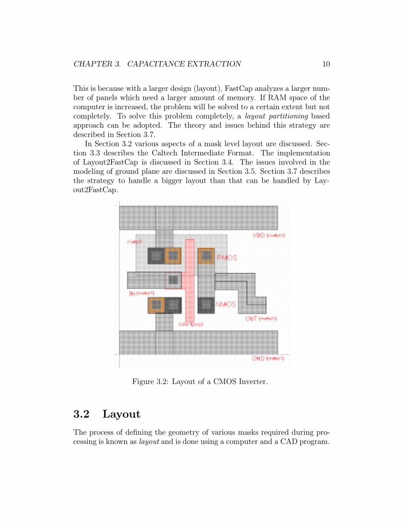
Figure 3.2: Layout of a CMOS Inverter.
3.2 Layout
The process of defining the geometry of various masks required during pro-cessing is known as layout and is done using a computer and a CAD program.
CHAPTER 3. CAPACITANCE EXTRACTION 11
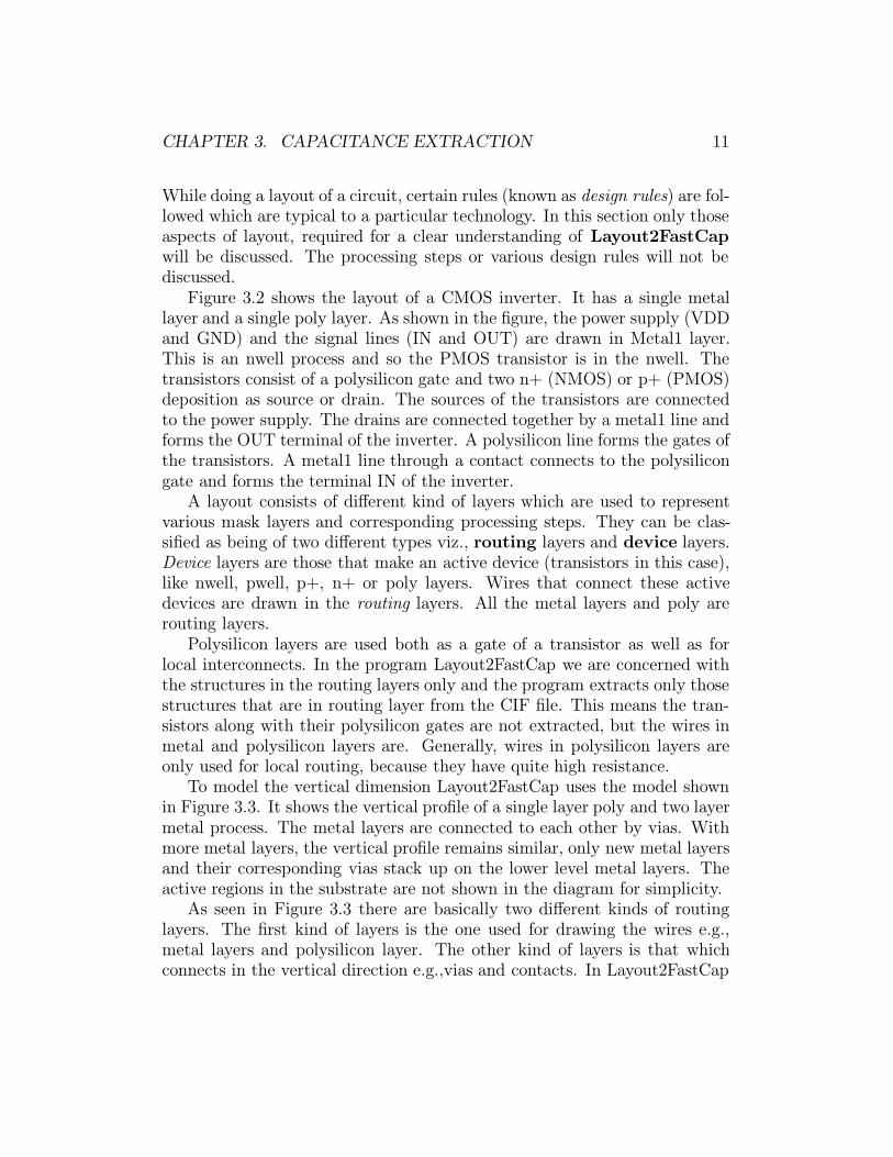
While doing a layout of a circuit, certain rules (known as design rules) are fol-lowed which are typical to a particular technology. In this section only thoseaspects of layout, required for a clear understanding of Layout2FastCapwill be discussed. The processing steps or various design rules will not bediscussed.
Figure 3.2 shows the layout of a CMOS inverter. It has a single metallayer and a single poly layer. As shown in the figure, the power supply (VDDand GND) and the signal lines (IN and OUT) are drawn in Metal1 layer.This is an nwell process and so the PMOS transistor is in the nwell. Thetransistors consist of a polysilicon gate and two n+ (NMOS) or p+ (PMOS)deposition as source or drain. The sources of the transistors are connectedto the power supply. The drains are connected together by a metal1 line andforms the OUT terminal of the inverter. A polysilicon line forms the gates ofthe transistors. A metal1 line through a contact connects to the polysilicongate and forms the terminal IN of the inverter.
A layout consists of different kind of layers which are used to representvarious mask layers and corresponding processing steps. They can be clas-sified as being of two different types viz., routing layers and device layers.Device layers are those that make an active device (transistors in this case),like nwell, pwell, p+, n+ or poly layers. Wires that connect these activedevices are drawn in the routing layers. All the metal layers and poly arerouting layers.
Polysilicon layers are used both as a gate of a transistor as well as forlocal interconnects. In the program Layout2FastCap we are concerned withthe structures in the routing layers only and the program extracts only thosestructures that are in routing layer from the CIF file. This means the tran-sistors along with their polysilicon gates are not extracted, but the wires inmetal and polysilicon layers are. Generally, wires in polysilicon layers areonly used for local routing, because they have quite high resistance.
To model the vertical dimension Layout2FastCap uses the model shownin Figure 3.3. It shows the vertical profile of a single layer poly and two layermetal process. The metal layers are connected to each other by vias. Withmore metal layers, the vertical profile remains similar, only new metal layersand their corresponding vias stack up on the lower level metal layers. Theactive regions in the substrate are not shown in the diagram for simplicity.
As seen in Figure 3.3 there are basically two different kinds of routinglayers. The first kind of layers is the one used for drawing the wires e.g.,metal layers and polysilicon layer. The other kind of layers is that whichconnects in the vertical direction e.g.,vias and contacts. In Layout2FastCap

CHAPTER 3. CAPACITANCE EXTRACTION 12
S U B S T R A T E
FIELD OXIDE
POLYSILICON
CONTACT
METAL1
VIA
METAL2
metal1Oxide
polyOxide
fieldOxide/2
metal2Layer
metal1Layer
polyLayer
Figure 3.3: Vertical Profile of a two layer metal and a single layer polyprocess. The variables 1 to in this figure are explained in Appendix B.
they are named as interconnect and contact layers respectively. From theprocess point of view this differentiation does not make sense because they aremade of the same material. The algorithms in Layout2FastCap differentiatebetween them because they have different characteristics. The structures inthe interconnect layers generally overlap each other. They span a larger areaof the layout and they can be polygons, wires, rectangles or round flashes(see Section 3.3). On the other hand the structures in the contact layers aresmaller in size and they are generally squares. Also they don’t overlap eachother.
The variables that are used to mark the dimensions in Figure 3.3 are theones that are used in the Process Data File. Process Data File is used byLayout2FastCap to build the third dimension of the two dimensional layout.One should be aware of the distances between various layers of metal andpoly and their thicknesses to construct the Process Data File. An exampleof Process Data File is presented in Appendix B.
CHAPTER 3. CAPACITANCE EXTRACTION 13
3.3 Caltech Intermediate Format
In this section only those aspects of Caltech Intermediate Format which arerequired for a good understanding of Layout2FastCap are described. Thedetails of the format are described in Appendix A.
In Caltech Intermediate Format (CIF) four geometric structures aredefined. They are
• Box. This is basically a rectangle and is described by the coordinatesof its center and its length and breadth.
• Polygon. This is described by a set of points which can be joined insuccession to create the polygon.
• Wire. This is described by its width and a set of points. The wire isthen the locus of this set of points within one-half width of the givenpath.
• Round Flash. This is described by the coordinates of its center andits diameter.
CIF also specifies the layer that these structures belong to.As shown in Figure 3.1, the layout should be converted to a CIF file
before it can be used by Layout2FastCap. Almost all the commercial layouteditors can convert a layout which is stored in their internal format to CIF.During the development of this program Cadence Design Systems’ layouteditor Virtuso was used. Using the export command of this layout editorCIF files were generated.
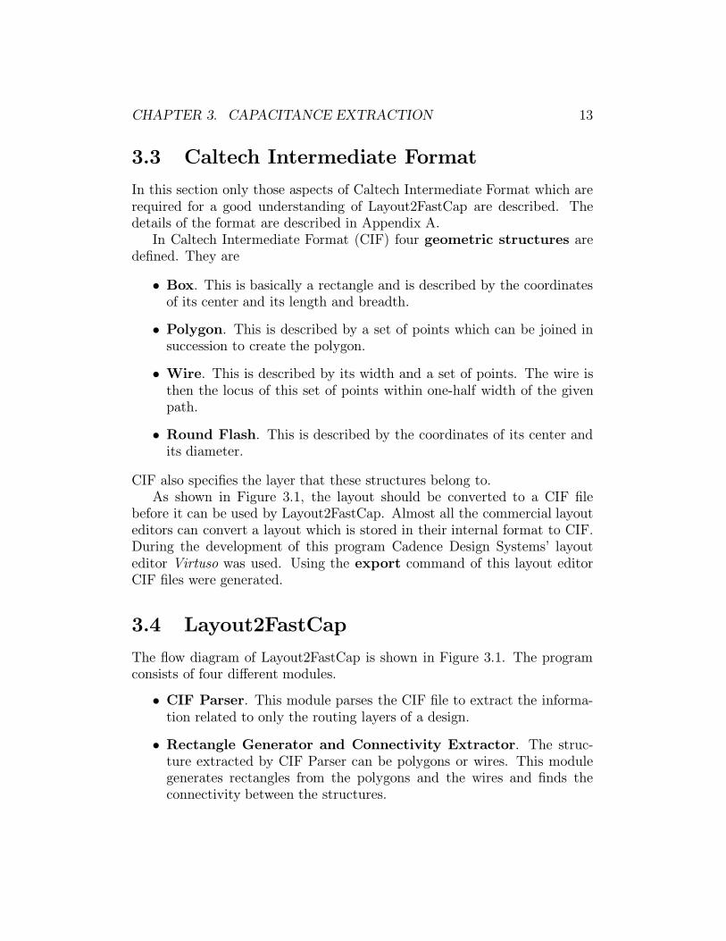
3.4 Layout2FastCap
The flow diagram of Layout2FastCap is shown in Figure 3.1. The programconsists of four different modules.
• CIF Parser. This module parses the CIF file to extract the informa-tion related to only the routing layers of a design.
• Rectangle Generator and Connectivity Extractor. The struc-ture extracted by CIF Parser can be polygons or wires. This modulegenerates rectangles from the polygons and the wires and finds theconnectivity between the structures.

CHAPTER 3. CAPACITANCE EXTRACTION 14
• 3 Dimensional Modeler. This module generates three dimensionalstructures from the two dimensional structures in the layout using theprocess information.
• Mesher. This module discretizes the surfaces of the three dimensionalstructures, so that they can be processed by a boundary element basednumerical solver. Here FastCap is used as the boundary element basednumerical solver.
In the rest of this section, each of these blocks will be considered and theirimplementation details will be discussed. The CMOS inverter of Figure 3.2will be 1 as each of the block is described and it will be shown what is theeffect of each block on the CMOS inverter layout.
3.4.1 CIF Parser
As shown in Figure 3.1 the CIF parser converts a CIF file to the internaldata structures of Layout2FastCap. The CIF file that is generated for theCMOS inverter layout of Figure 3.2 is given below.
(CIF file written on 01-Mar-1998 15:21:38 by CADENCE);DS 1 1 1;9 INV;L MET1;B 3810 570 1905,285;94 OUT 2865,1785;94 IN 645,1785;94 GND 3075,300; 94 VDD 3255,3270;W 400 1300,1800 395,1800;W 400 2510,1770 3075,1770 3075,1200 3340,1200;
P 1890,990 2295,990 2295,2565 1890,2565;94 OUT 2085,1755;P 885,0 1290,0 1290,1005 885,1005;P 690,990 1485,990 1485,1380 690,1380; B 3810 570 1905,3300;P 885,2580 1290,2580 1290,3585 885,3585;P 690,2190 1485,2190 1485,2580 690,2580;L CONT;B 210 210 900,1200;B 210 210 1305,1200;B 210 210 2100,1215; B 210 210 2100,2385;B 210 210 900,2385;B 210 210 1305,2385; B 210 210 1305,1800;L POLY;94 IN 1665,840;P 1800,795 1605,795 1605,1590 1110,1590
1110,1995 1605,1995 1605,2790 1800,2790;L N+;P 1890,990 2295,990 2295,1380 1890,1380;P 1095,990 1500,990 1500,1380 1095,1380;P 690,2190 1095,2190 1095,2580 690,2580;L P+;P 690,990 1095,990 1095,1380 690,1380;
CHAPTER 3. CAPACITANCE EXTRACTION 15
P 1890,2190 2295,2190 2295,2580 1890,2580;P 1095,2190 1500,2190 1500,2580 1095,2580;L NWELL;B 2190 990 1500,2400;DF;C 1;
E
To understand the legend of the above CIF file one should refer to Ap-pendix A where a brief overview of Caltech Intermediate Format is given.The CIF 9 is written using flex and bison which are gnu version of lex andyacc. The parser reads the CIF file to extract the layer and geometry in-formation. It selects only those geometric structures that are in the routinglayers i.e., poly, metal or via layers.
Figure 3.4 shows how the CMOS inverter of Figure 3.2 will look after itis processed by CIF parser. Various geometric structures are labeled in theFigure 3.4. The net in the poly layer is a polygon. There are two wires inmetal1 layer. Rest of the structures in metal1 layer are boxes. There wereno round flashes in the original layout (see Figure 3.2) The conductor namesand number are also labeled in the figure. There are four conductors - IN,VDD, GND and OUT.
It was found that the same layer can be referred by different names inthe technology file for a particular process. As a result the CIF file will havedifferent names for the same layer, e.g. metal1 layer can be referred to asMET1 or METAL1. However, Layout2FastCap uses unique internal namesto label each layer and a Layer Mapping File is provided to map the internalnames in Layout2FastCap to the names in the CIF file. An example of thisLayer Mapping File is given in Appendix B.
Round flash are converted to squares when they are extracted from theCIF file. This is an approximation. The side of the square is equal to thediameter of the round flash. This is illustrated in Figure 3.5.
The parser stores all the extracted geometric structures in three lists.The boxes and round flashes (converted to squares) are stored in one list.The polygons and wires are stored in the other two lists. For each of thesegeometric structure a C language data structure is used to store the informa-tion. Each C language data structure stores the geometry information andlayer information for the boxes, round flashes, polygons and wires. So, thelists are basically the list of structures.

CHAPTER 3. CAPACITANCE EXTRACTION 16
Figure 3.4: Extraction of routing layers from the layout of the CMOS in-verter.
DS
Figure 3.5: Conversion of a round flash to a square.

CHAPTER 3. CAPACITANCE EXTRACTION 17
3.4.2 Rectangle Generator & Connectivity Extractor
The lists returned by the CIF parser are analyzed by the Rectangle Gener-ator & Connectivity Extractor module of Layout2FastCap. It converts thepolygons and wires to rectangles. Boxes are rectangles and the round flasheshave already been converted to rectangles and hence the list of rectangles iskept unchanged.
There is a reason why the polygons and the wires are converted to rect-angles. When we want to mesh a three dimensional structure of a polygonor of a wire, we need to identify the rectangles constituting them. So, in-stead of using separate algorithms for meshing for all the different structures,the polygons and wires are converted to rectangles before hand. This bringsmodularity to the code at an early stage.
The conversion strategies are detailed below.
• Polygons
1
2 3 4 5
6 7sweep
Figure 3.6: Conversion of a manhattan shaped polygon to rectangles.
Layout2FastCap can analyze only manhattan shaped (rectilinear) poly-gons. This kind of polygon is generally used in a layout. Figure 3.6illustrates the idea behind this conversion process. An imaginary line(shown in the diagram as a dotted line) is sweeped from left to right.As this line meets the edges of the polygon, it forms a rectangle. Asshown in Figure 3.6 seven rectangles are formed from the given poly-gon. The smallest width of the rectangle that will be generated by thismethod depends on the grid size of the layout editor.
CHAPTER 3. CAPACITANCE EXTRACTION 18
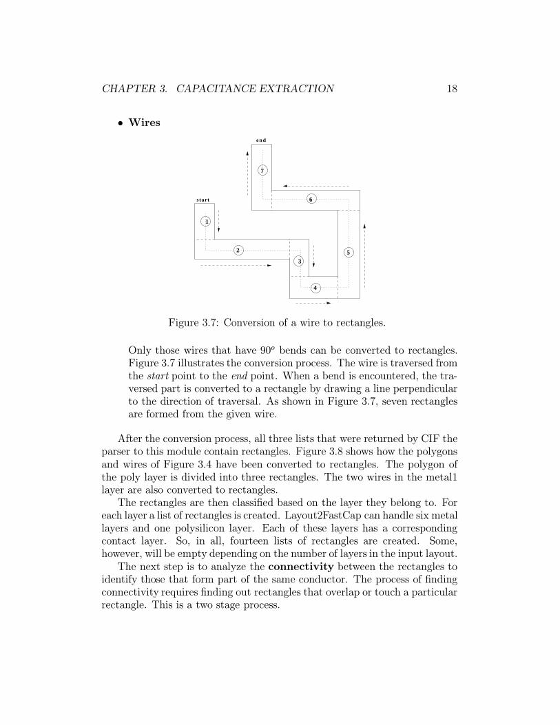
• Wires
start
end
4
5
6
7
1
2
3
Figure 3.7: Conversion of a wire to rectangles.
Only those wires that have 90o bends can be converted to rectangles.Figure 3.7 illustrates the conversion process. The wire is traversed fromthe start point to the end point. When a bend is encountered, the tra-versed part is converted to a rectangle by drawing a line perpendicularto the direction of traversal. As shown in Figure 3.7, seven rectanglesare formed from the given wire.
After the conversion process, all three lists that were returned by CIF theparser to this module contain rectangles. Figure 3.8 shows how the polygonsand wires of Figure 3.4 have been converted to rectangles. The polygon ofthe poly layer is divided into three rectangles. The two wires in the metal1layer are also converted to rectangles.
The rectangles are then classified based on the layer they belong to. Foreach layer a list of rectangles is created. Layout2FastCap can handle six metallayers and one polysilicon layer. Each of these layers has a correspondingcontact layer. So, in all, fourteen lists of rectangles are created. Some,however, will be empty depending on the number of layers in the input layout.
The next step is to analyze the connectivity between the rectangles toidentify those that form part of the same conductor. The process of findingconnectivity requires finding out rectangles that overlap or touch a particularrectangle. This is a two stage process.

CHAPTER 3. CAPACITANCE EXTRACTION 19
As a first step, only those rectangles are analyzed that are in the sameinterconnect or contact layer. Each group of connected rectangles is givena unique number called conductor number and this group comprises aconductor. This type of connectivity is known as intralayer connectivity.
(a)
(b)
Figure 3.8: Conversion of Polygon and Wires to rectangles for both metal1and poly layer: (a) poly; and (b) metal1
The second step is to find the connectivity between the rectangles thatare in adjacent layers. For a given interconnect layer the upper and lowercontact layers are the adjacent layers. The idea here, is to take a particularrectangle in an interconnect layer and find if any rectangle in the adjacentcontact layers touches or overlaps this rectangle. The conductor numbers thatwere assigned in the first step are reassigned in this stage as connectivity isestablished between various interconnect layers. This type of connectivity isknown as interlayer connectivity. These two types of analyses are describedbelow.
• Intralayer Connectivity
As the name suggests, in this process, the connectivity of rectanglesbelonging to the same layer is determined. Interconnect and contactlayers are handled differently.
CHAPTER 3. CAPACITANCE EXTRACTION 20
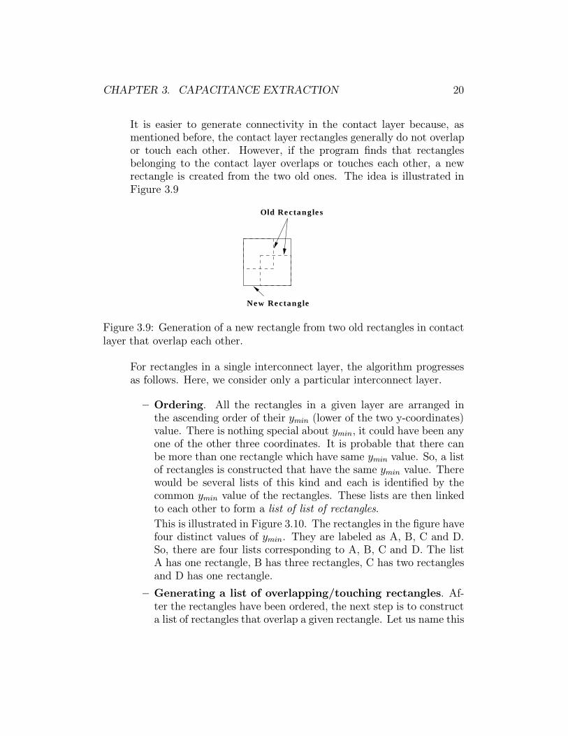
It is easier to generate connectivity in the contact layer because, asmentioned before, the contact layer rectangles generally do not overlapor touch each other. However, if the program finds that rectanglesbelonging to the contact layer overlaps or touches each other, a newrectangle is created from the two old ones. The idea is illustrated inFigure 3.9
Old Rectangles
New Rectangle
Figure 3.9: Generation of a new rectangle from two old rectangles in contactlayer that overlap each other.
For rectangles in a single interconnect layer, the algorithm progressesas follows. Here, we consider only a particular interconnect layer.
– Ordering. All the rectangles in a given layer are arranged inthe ascending order of their ymin (lower of the two y-coordinates)value. There is nothing special about ymin, it could have been anyone of the other three coordinates. It is probable that there canbe more than one rectangle which have same ymin value. So, a listof rectangles is constructed that have the same ymin value. Therewould be several lists of this kind and each is identified by thecommon ymin value of the rectangles. These lists are then linkedto each other to form a list of list of rectangles.
This is illustrated in Figure 3.10. The rectangles in the figure havefour distinct values of ymin. They are labeled as A, B, C and D.So, there are four lists corresponding to A, B, C and D. The listA has one rectangle, B has three rectangles, C has two rectanglesand D has one rectangle.
– Generating a list of overlapping/touching rectangles. Af-ter the rectangles have been ordered, the next step is to constructa list of rectangles that overlap a given rectangle. Let us name this

CHAPTER 3. CAPACITANCE EXTRACTION 21
Y
XA
B
C
D
D1
C2
B3B2B1
A1
C1
Figure 3.10: Rectangles in a typical interconnect layer.
list as OverlapList. The procedure described below is repeatedfor each rectangle of the list of list of rectangles.
From the list of the list of rectangles, consider a particular rect-angle of a particular list. In general, this rectangle may overlap ortouch any other rectangle that is in its list. So, all the rectanglesin its list are checked and those rectangles which overlap or touchthis given rectangle are put in its OverlapList. The rectangles thatare in the lists whose ymin value is less than the ymin value of thecurrent list are not considered. This is because lists are scannedin the ascending order of ymin value. Also, those lists whose yminvalue is more than the ymax (higher of the two y-coordinates of arectangle) of the given rectangle are not considered, because therectangles belonging to those lists won’t overlap or touch the givenrectangle. So, now the remaining lists are considered and all therectangles in these lists are checked with the given rectangle. Therectangles that overlap or touch the given rectangle are put in itsOverlapList.
This idea is illustrated in Figure 3.10. Let the given rectanglebe B2 of list B. In the list B, it overlaps with B1 only and notwith B3. So, B1 is put in the OverlapList of B2. List A is not

CHAPTER 3. CAPACITANCE EXTRACTION 22
considered because its ymin value is less than the ymin value of listB. Also, list D is not considered because its ymin value is more thanthe ymax of rectangle B2. So, the only list that is considered is listC. It is found that only C1 should be added to the OverlapList ofB2.
– Generation of new rectangles. There are various ways a rect-angle can overlap another rectangle as evident from Figure 3.10.All these cases have been implemented in the code. When a rect-angle overlaps another rectangle new rectangles are generated andadded to the ordered list. The old rectangles are removed fromthe ordered list. When a rectangle touches another rectangle newrectangles are not generated but this information is added to theC-structure of the rectangle.
Following the above three steps, intralayer connectivity of rectangles inthe interconnect layer is established.
• Interlayer Connectivity
As the name suggests, in this case, the connectivity between rectanglesbelonging to adjacent layers is determined. A rectangle in an inter-connect layer is considered and those rectangles are searched for inthe upper and lower contact layers that overlap or touches the givenrectangle.
After the connectivity has been established each rectangle has a conductornumber. The highest conductor number indicates the number of conductorsin the design.
3.4.3 Three Dimensional Modeler
After asserting connectivity (using the process information in Process DataFile - see Appendix B), the two dimensional rectangles are converted to threedimensional structures. The process information comes from the technologyand the user has to provide this to Layout2FastCap.
The process information consists of the thickness of various layers (poly,metal1, metal2 etc.,) and the distance between various layers. In other wordsall the variables in Figure 3.3 should be assigned a certain value accordingto the process. This gives the third dimension to all of the two dimensionalstructures.
CHAPTER 3. CAPACITANCE EXTRACTION 23
Layout2FastCap has the option of generating three dimensional structureswith either rectangular or trapezoidal cross section. Trapezoidal cross sectionis a more realistic way of modeling a three dimensional interconnect. Atpresent Layout2FastCap can model trapezoidal cross section only for simplestructures which do not have any bends.
3.4.4 Mesher
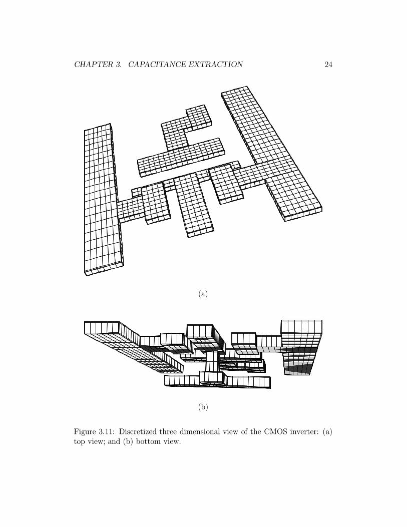
As discussed in Chapter 2, all boundary element based numerical solversrequire that the surfaces of the three dimensional conductors be discretized.Discretization implies that the surfaces are subdivided into small rectanglesor triangles. Layout2FastCap generates rectangular panels. Edges of theconductors are modeled differently. The width of the edge panels is 10% ofthe width of the inner panels. This is because charges accumulate at sharpedges and corners. As a result, there exists a charge gradient from the edge ofthe conductor to the inner part of the conductor. To model this accuratelythe edge panels are made smaller in size. Two views of the meshed threedimensional view of the CMOS inverter is shown in Figure 3.11.
The panel size is a deciding factor for the execution speed and accuracyof FastCap. Smaller panel size results in larger number of panels and henceslower execution of FastCap. Smaller panel size, however, ensures higheraccuracy. The user controls the size of the panels using two variables. Thefirst is the minimum panel size and the second is the maximum numberof panels along a given straight length of a conductor. This optimizes thenumber of panels and maintains a balance between speed and accuracy.
3.4.5 Limitations of Layout2FastCap
Layout2FastCap has several limitations. Some of them can be solved withminor changes in the code, but these were not deemed necessary at this point.The limitations are listed below.
1. The major limitation of Layout2FastCap is that it can 2 only a smalllayout with reasonable accuracy. To solve larger designs a layout par-titioning approach was adopted and is described in Section 3.7.
2. Layout2FastCap can handle only those polygons that are manhattanshaped. Polygons that are not of this shape are rarely used.
CHAPTER 3. CAPACITANCE EXTRACTION 24
(a)
(b)
Figure 3.11: Discretized three dimensional view of the CMOS inverter: (a)top view; and (b) bottom view.

CHAPTER 3. CAPACITANCE EXTRACTION 25
3. The wires that can be handled by Layout2FastCap can have only 90o
bends. Most of the automatic routers draw wires of only this kind. Ina custom design this would be a limitation.
4. Layout2FastCap is hardcoded to handle no more than six metal layers.This restriction is not a limitation for current technology and can beremoved very easily when necessary.
5. Layout2FastCap models the vertical dimension for those processes whichuse planarization. This makes the modeling simpler and at presentmost of the processes use CMP for planarization.
3.5 Modeling of Ground Plane
So far in our discussion we have not talked about the ground plane. Thesubstrate in a chip acts as the ground plane. It is the major source ofcapacitance for the lower level interconnects i.e., the interconnects that arenear to the substrate of the chip. Upper layer interconnects (say metal3 andup) are shielded by the lower layer interconnects. This is one of the primereason why there are long global nets in the upper metal layers. In the restof this section various issues involved in the modeling of ground plane arediscussed. An image method based technique is developed that simulates theground plane as an ideal infinitely large sheet of conductor.
3.5.1 Assumptions
The substrate is not as conducting as the metal1 or even poly layers. So, fewassumptions are required to model the chip substrate as the ground plane. Aspointed out in Chapter 2, FastCap can only analyze ideal conductors embed-ded in a uniform dielectric medium. The conductors analyzed by FastCapare assumed to have infinite conductivity, so that the charges accumulateonly at the surfaces. So, we assume the following while modeling the chipsubstrate as ground plane in FastCap.
• Perfect conductor. This assumption is necessary to simulate the chipsubstrate as a ground plane in FastCap. This is one of the inherentlimitation of FastCap.
• Infinite Sheet. This assumption will allow us to use an ImageMethod [25] (described later in this Section) to simulate the ground

CHAPTER 3. CAPACITANCE EXTRACTION 26
plane. This assumption is quite valid because the size of the layout thatis analyzed by Layout2FastCap is quite small compared to the wholedesign. So, the size of the chip substrate will be much much biggerthan the dimensions of the interconnects in the input layout. So, wecan assume the ground to extend to infinity. Since, it allows us to usethe image method it also speeds up the execution of FastCap.
3.5.2 Image Method
The idea behind the Image Method [25] is illustrated in Figure 3.12. Fig-ure 3.12(a) shows the cross section of a conductor on the ground plane. Theconductor is at a distance D from the ground plane. When 1 volt is applied tothe conductor and the ground plane is at 0 volts let us try to find the chargeon the conductor. The charge on the conductor is the capacitance of theconductor with respect to ground because the potential difference betweenthe conductor and the ground is 1 volt. Classically, this is a difficult problemto solve. An equivalent configuration for this is two conductors separated bya distance 2D in space (see Figure 3.12(b)) with 1 volt applied to the upperconductor and -1 volt applied to the lower conductor. The lower conductoris the image of the upper conductor. If we can solve for electric field for thisequivalent configuration, then it will be valid for the original configuration.
D2D
Image Conductor
ConductorConductor
Real Ground Plane
(b)(a)
Plane of Symmetry
Figure 3.12: Illustration of Image Method: (a) a conductor over a groundplane; and (b) equivalent configuration with the image of the conductor.
Using the idea stated above, FastCap can be used to solve a problemwith interconnects over a ground plane. So, instead of determining the ca-pacitance between an interconnect and ground, the capacitance between an

CHAPTER 3. CAPACITANCE EXTRACTION 27
interconnect and its image will be determined. Since we are solving a differentproblem than the original problem, we need to reinterprate the capacitancematrix generated by FastCap.
3.5.3 Single Conductor Over Ground Plane
To solve a single conductor over ground problem, FastCap solves a two con-ductor problem as illustrated in Figure 3.12. Figure 3.13 shows the twoconfigurations used by FastCap to solve a two body problem. The circlethat includes both the conductors represents infinity i.e., the field lines thatoriginate from one of the conductors, but do not terminate on the other. So,an equivalent amount of charge will be there on this fictitious enclosure.
QA
QAI Q
QB
BI-
-+1V
0V +1V
0V
0V +1VC C
1sC C
1 1
1+1V 0V
1
-Q AR-Q BR
Configuration A Configuration B
1’s
11’11’
1’ 1’
1’ 1’
Plane of Symmetry
Figure 3.13: Two configurations used by FastCap to generate the 2 × 2capacitance matrix for a two body problem.
Here, conductor 1’ is the image of conductor 1. In configuration A, con-ductor 1 is at 1 volt and conductor 1’ is at 0 volts. In this situation, chargeof amount QA is induced on conductor 1 and −QAI and −QAR on conductor1’ and the enclosure respectively. Configuration B is the reciprocal of config-uration A. Here, conductor 1 is at 0 volts and 1 volt is applied to conductor1’. In this situation, charge of amount QB is induced on conductor 1 and−QBI and −QBR on conductor 1’ and the enclosure respectively.
CHAPTER 3. CAPACITANCE EXTRACTION 28
Using the principle of charge neutrality, we obtain:
QA = QAI +QAR
QB = QBI +QBR
(3.1)
Here, QA, QAI , QAR, QB, QBI and QBR are all positive quantities. Thesecharges are related to the capacitances of the capacitance matrix for the twobody problem. The capacitance matrix for two conductors is
C =
[c11 −c11′
−c11′ c1′1′
](3.2)
Here, c11 and c1′1′ are the total capacitance of conductor 1 and 1’ respectively.They are the sum of the coupling capacitance and the self capacitance of theconductors. The self capacitances and coupling capacitances are shown inthe capacitance models of Figure 3.13. Also, c11, c11′ and c1′1′ are all positivequantities. Since unit potential is applied on the conductors, the chargeinduced on them are the capacitances. So, we can relate the charges on theconductors and the capacitances in the capacitance matrix as,
QA = c11
QAI = c11′
QAR = c1s = c11 − c11′
(3.3)
QB = c11′
QBI = c1′1′
QBR = c1′s = c1′1′ − c11′
(3.4)
Now that we have got an idea of how FastCap solves a two body problemand what each entry in the capacitance matrix means, let us get back to theoriginal problem as shown in Figure 3.12. Figure 3.14 shows the problemthat we want to solve. Our aim is to solve the problem in configuration G.Configuration C is the equivalent Image Method formulation of configurationG. So, if we solve the problem in Configuration C, it is the solution of theproblem in configuration G. In configuration G, 1 volt is applied to the con-ductor and the ground plane is at 0 volts. QG amount of charge is inducedon the conductor and an equal and opposite amount of charge is induced onthe ground plane. In the corresponding image method formulation (Config-uration C), the conductor is at 1 volt and its image is at -1 volt. QC amount
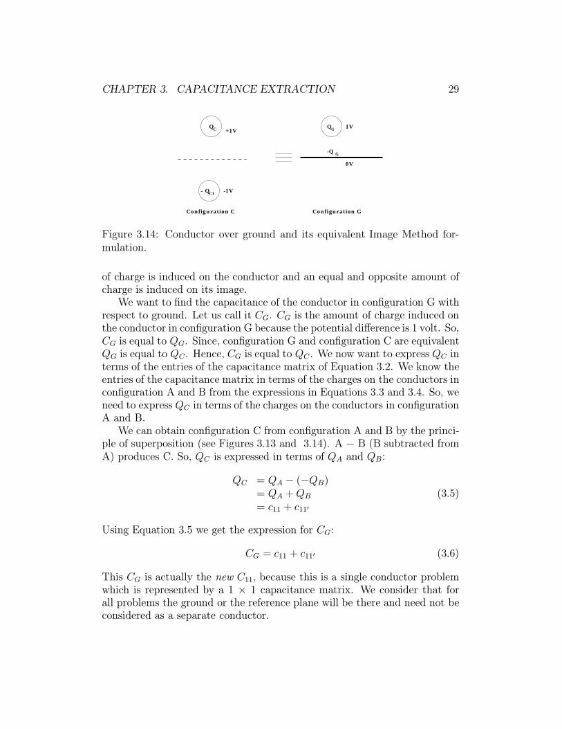
CHAPTER 3. CAPACITANCE EXTRACTION 29
Q
Q
Q
-
+1VC
CI -1V
1VG
-Q G
0V
Configuration C Configuration G
Figure 3.14: Conductor over ground and its equivalent Image Method for-mulation.
of charge is induced on the conductor and an equal and opposite amount ofcharge is induced on its image.
We want to find the capacitance of the conductor in configuration G withrespect to ground. Let us call it CG. CG is the amount of charge induced onthe conductor in configuration G because the potential difference is 1 volt. So,CG is equal to QG. Since, configuration G and configuration C are equivalentQG is equal to QC. Hence, CG is equal to QC. We now want to express QC interms of the entries of the capacitance matrix of Equation 3.2. We know theentries of the capacitance matrix in terms of the charges on the conductors inconfiguration A and B from the expressions in Equations 3.3 and 3.4. So, weneed to express QC in terms of the charges on the conductors in configurationA and B.
We can obtain configuration C from configuration A and B by the princi-ple of superposition (see Figures 3.13 and 3.14). A − B (B subtracted fromA) produces C. So, QC is expressed in terms of QA and QB:
QC = QA − (−QB)= QA +QB
= c11 + c11′
(3.5)
Using Equation 3.5 we get the expression for CG:
CG = c11 + c11′ (3.6)
This CG is actually the new C11, because this is a single conductor problemwhich is represented by a 1 × 1 capacitance matrix. We consider that forall problems the ground or the reference plane will be there and need not beconsidered as a separate conductor.
CHAPTER 3. CAPACITANCE EXTRACTION 30
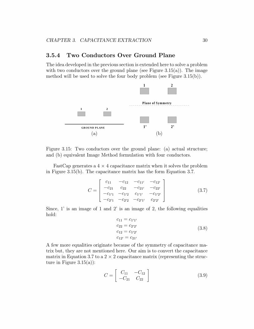
3.5.4 Two Conductors Over Ground Plane
The idea developed in the previous section is extended here to solve a problemwith two conductors over the ground plane (see Figure 3.15(a)). The imagemethod will be used to solve the four body problem (see Figure 3.15(b)).
1 2
GROUND PLANE
1 2
2’1’
Plane of Symmetry
(a) (b)
Figure 3.15: Two conductors over the ground plane: (a) actual structure;and (b) equivalent Image Method formulation with four conductors.
FastCap generates a 4 × 4 capacitance matrix when it solves the problemin Figure 3.15(b). The capacitance matrix has the form Equation 3.7.
C =
c11 −c12 −c11′ −c12′
−c21 c22 −c21′ −c22′
−c1′1 −c1′2 c1′1′ −c1′2′
−c2′1 −c2′2 −c2′1′ c2′2′
(3.7)
Since, 1’ is an image of 1 and 2’ is an image of 2, the following equalitieshold:
c11 = c1′1′
c22 = c2′2′
c12 = c1′2′
c12′ = c21′
(3.8)
A few more equalities originate because of the symmetry of capacitance ma-trix but, they are not mentioned here. Our aim is to convert the capacitancematrix in Equation 3.7 to a 2 × 2 capacitance matrix (representing the struc-ture in Figure 3.15(a)):
C =
[C11 −C12
−C21 C22
](3.9)

CHAPTER 3. CAPACITANCE EXTRACTION 31
We need to find only C11 and C12 (Equation 3.9) in terms of the entries ofthe capacitance matrix of Equation 3.7. This is because C21 is same as C12,and C22 will have the same form of C11 with only the subscripts 1 and 1’replaced by 2 and 2’ respectively.
Consider the configuration in Figure 3.16 where there are two conductorsover ground. A potential of 1 volt is applied to conductor 1, and the groundplane, and the conductor 2 are at 0 volts. This configuration enables thecapacitances C11 and C12 to be related to the charges on the conductor.The corresponding image method formulation is not illustrated, as we haveshown this in the case of the single conductor problem. Here, the imagemethod formulation yields two more conductors below the ground plane.These additional conductors are mirror images of the original conductorsabout the ground plane.
-Q G
-Q 0V1V 2Q1
1 2
0V
Figure 3.16: Two conductors over the ground plane.
Relating the charges in Figure 3.16 and the capacitances in Equation 3.9we have,
Q1 = C11
Q2 = C12(3.10)
In this case, FastCap solves a four body problem and four configurationsare examined by FastCap. Figure 3.17 illustrates the four configurations.The two configurations in Figures 3.17(a) and (b) are only required to deriveexpressions for C11 and C12.
Equation 3.11 relates the charges on the conductor in Figure 3.17 to theentries in the capacitance matrix of Equation 3.7.
Q1A = c11
Q2A = c12
Q1B = c11′
Q2B = c1′2
(3.11)

CHAPTER 3. CAPACITANCE EXTRACTION 32
Now, the superposition principle relates the charges in the two configurationsof Figure 3.17 to the charges in Figure 3.16. It is clear that the image methodversion of Figure 3.16 is equivalent to configuration A − B of Figure 3.17.We obtain the following expressions:
Q1 = Q1A − (−Q1B)= Q1A +Q1B
= c11 + c11′
−Q2 = −Q2A− (−Q2B)Q2 = Q2A −Q2B
= c12 − c1′2
(3.12)
Q
0V
1A
0V
0V2A-Q+1V
Configuration A
1
1’ 2’
2
0V
0V-Q
Configuration B
0V
+1V
1B 2B-Q
1
1’
2
2’
(a) (b)
0V 0V
+1V0V-Q Q1C 2C
21
1’ 2’
Configuration C
0V-Q0V-Q
1
1’
2
2’
Configuration D
1D 2D
0V +1V
(c) (d)
Figure 3.17: The four configurations used by FastCap to solve the four bodyproblem.
Equation 3.10 and Equation 3.11 relate the charges in Equation 3.12 tothe entries of the capacitance matrix of Equation 3.7 and Equation 3.9. From
CHAPTER 3. CAPACITANCE EXTRACTION 33
these equations, we can derive the expression for C11 and C12. C21 and C22
follow from them.C11 = c11 + c11′
C12 = C21 = c12 − c1′2
C22 = c22 + c22′
(3.13)
We have the following 2 × 2 matrix generated from the original 4 × 4 matrix(Equation 3.14).
C =
[c11 + c11′ −(c12 − c1′2)−(c21 − c1′2) c22 + c22′
](3.14)
3.5.5 Generalization of the solution
This idea can be extended to a three conductors over ground plane problemand if we follow the above steps, we will obtain the following 3 × 3 ca-pacitance matrix from the 6 × 6 capacitance matrix generated by FastCap.(Equation 3.15).
C =
(c11 + c11′) −(c12 − c1′2) −(c13 − c1′3)−(c21 − c1′2) (c22 + c22′) −(c23 − c2′3)−(c13 − c1′3) −(c23 − c2′3) (c33 + c33′)
(3.15)
From Equations. 3.14 and 3.15 we can observe a trend which will allow usto generalize the idea to a problem of n conductors over ground plane. Withthe images, FastCap will solve a problem of 2n conductors and will generatea 2n × 2n capacitance matrix. Our aim is to change this to an n × ncapacitance matrix as shown in Figure 3.18.
A B
CM
Dn x n
2n x 2n
Figure 3.18: Conversion of a 2n × 2n capacitance matrix resulting fromapplication of the image method to an n × n capacitance matrix.
For the two conductors over ground plane problem, the A and B matrixof Figure 3.18 can be represented by the Equations. 3.16 and 3.17. The
CHAPTER 3. CAPACITANCE EXTRACTION 34
entries are taken from the capacitance matrix of Equation 3.7.
A =
[c11 −c12
−c21 c22
](3.16)
B =
[−c11′ −c12′
−c21′ −c22′
](3.17)
To obtain the capacitance matrix of Equation 3.14 we need to subtract matrixB from matrix A.
A−B =
[c11 + c11′ −(c12 − c1′2)−(c21 − c1′2) c22 + c22′
](3.18)
The capacitance matrix of Equation 3.18 is exactly same as that of the ca-pacitance matrix of Equation 3.14. This is also observed in case of threeconductors over ground plane problem. Hence, we have the following gener-alized expression (Equation 3.19) for converting the 2n × 2n capacitancematrix of Figure 3.18 to an n × n capacitance matrix.
M = A−B (3.19)
This expression will be used in the next section to interpret the capacitancematrix generated by FastCap for the CMOS inverter.
3.6 Interpretation of the Capacitance Matrix
of the CMOS Inverter
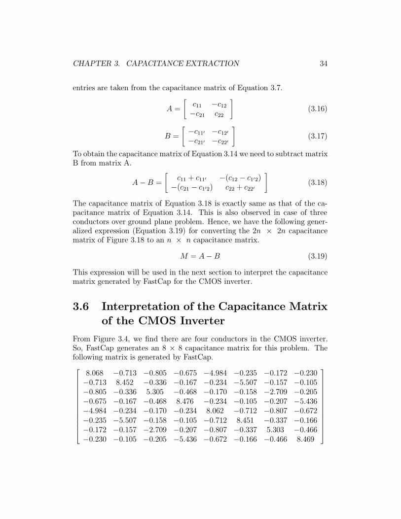
From Figure 3.4, we find there are four conductors in the CMOS inverter.So, FastCap generates an 8 × 8 capacitance matrix for this problem. Thefollowing matrix is generated by FastCap.
8.068 −0.713 −0.805 −0.675 −4.984 −0.235 −0.172 −0.230−0.713 8.452 −0.336 −0.167 −0.234 −5.507 −0.157 −0.105−0.805 −0.336 5.305 −0.468 −0.170 −0.158 −2.709 −0.205−0.675 −0.167 −0.468 8.476 −0.234 −0.105 −0.207 −5.436−4.984 −0.234 −0.170 −0.234 8.062 −0.712 −0.807 −0.672−0.235 −5.507 −0.158 −0.105 −0.712 8.451 −0.337 −0.166−0.172 −0.157 −2.709 −0.207 −0.807 −0.337 5.303 −0.466−0.230 −0.105 −0.205 −5.436 −0.672 −0.166 −0.466 8.469
CHAPTER 3. CAPACITANCE EXTRACTION 35
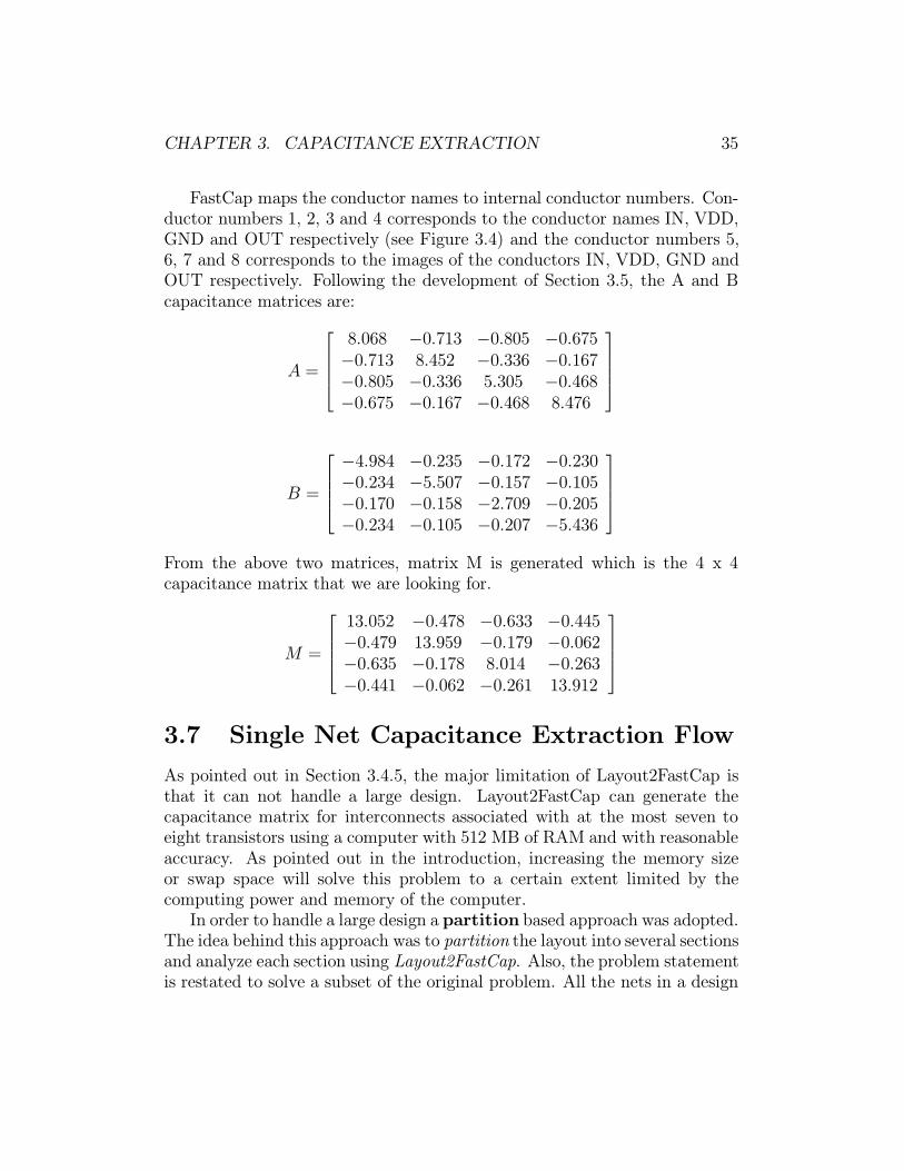
FastCap maps the conductor names to internal conductor numbers. Con-ductor numbers 1, 2, 3 and 4 corresponds to the conductor names IN, VDD,GND and OUT respectively (see Figure 3.4) and the conductor numbers 5,6, 7 and 8 corresponds to the images of the conductors IN, VDD, GND andOUT respectively. Following the development of Section 3.5, the A and Bcapacitance matrices are:
A =
8.068 −0.713 −0.805 −0.675−0.713 8.452 −0.336 −0.167−0.805 −0.336 5.305 −0.468−0.675 −0.167 −0.468 8.476
B =
−4.984 −0.235 −0.172 −0.230−0.234 −5.507 −0.157 −0.105−0.170 −0.158 −2.709 −0.205−0.234 −0.105 −0.207 −5.436
From the above two matrices, matrix M is generated which is the 4 x 4capacitance matrix that we are looking for.
M =
13.052 −0.478 −0.633 −0.445−0.479 13.959 −0.179 −0.062−0.635 −0.178 8.014 −0.263−0.441 −0.062 −0.261 13.912
3.7 Single Net Capacitance Extraction Flow
As pointed out in Section 3.4.5, the major limitation of Layout2FastCap isthat it can not handle a large design. Layout2FastCap can generate thecapacitance matrix for interconnects associated with at the most seven toeight transistors using a computer with 512 MB of RAM and with reasonableaccuracy. As pointed out in the introduction, increasing the memory sizeor swap space will solve this problem to a certain extent limited by thecomputing power and memory of the computer.
In order to handle a large design a partition based approach was adopted.The idea behind this approach was to partition the layout into several sectionsand analyze each section using Layout2FastCap. Also, the problem statementis restated to solve a subset of the original problem. All the nets in a design
CHAPTER 3. CAPACITANCE EXTRACTION 36
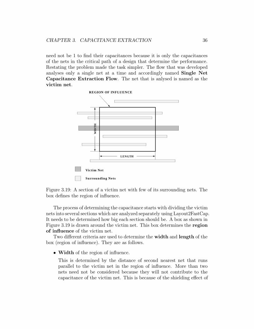
need not be 1 to find their capacitances because it is only the capacitancesof the nets in the critical path of a design that determine the performance.Restating the problem made the task simpler. The flow that was developedanalyses only a single net at a time and accordingly named Single NetCapacitance Extraction Flow. The net that is anlysed is named as thevictim net.
WID
TH
LENGTH
Victim Net
Surrounding Nets
REGION OF INFLUENCE
Figure 3.19: A section of a victim net with few of its surrounding nets. Thebox defines the region of influence.
The process of determining the capacitance starts with dividing the victimnets into several sections which are analyzed separately using Layout2FastCap.It needs to be determined how big each section should be. A box as shown inFigure 3.19 is drawn around the victim net. This box determines the regionof influence of the victim net.
Two different criteria are used to determine the width and length of thebox (region of influence). They are as follows.
• Width of the region of influence.
This is determined by the distance of second nearest net that runsparallel to the victim net in the region of influence. More than twonets need not be considered because they will not contribute to thecapacitance of the victim net. This is because of the shielding effect of
CHAPTER 3. CAPACITANCE EXTRACTION 37
the two nearest conductors. Very few field lines will be there betweenthe victim net and the third nearest net. Only one of the nearest netneed to be considered if the nearest net runs parallel to the victim netalong the complete length of the region of influence. But, this does nothappen very often. So, most of the time it is the distance to the secondnearest net that determines the width.
• Length of the region of influence.
After the width of the box is determined, the length is determined fromthe maximum area that a region of influence can have. The maximumarea is limited by the largest design that Layout2FastCap can handle.This corresponds to the maximum number of panels that FastCap cananalyze which is limited by the memory available in a given computer.Few test runs are needed to identify this number. An Ultra 1 SunSparcstation with 512 MB of RAM can handle somewhere between10 thousands and 20 thousands of panels depending on the relativeposition of the panels. The next thing that needs to be consideredfor determining the maximum area is how dense the meshing will beand what the vertical dimensions are. Using all the above informationthe maximum area is estimated and from there length of the region ofinfluence is determined.
Let us consider Figure 3.19 again. The box as shown in this figure willbe repeated along the length of the wire and conductors inside each boxwill be analyzed by FastCap. The problem that arises because of this is theaccumulation of artificial charges at the edges of the nets where they are cut:FastCap does not know that the net does not end there. The effect of thiswill be an artificial increase in the amount of capacitance. This problem issolved using the Artificial Boundary Charge Correction Scheme. Thescheme is illustrated in Figure 3.20.
The idea behind this scheme is novel but very simple. There are twotypes of boxes in Figure 3.20. These are outer boxes and inner boxes.FastCap (after using Layout2FastCap) calculates the capacitance of all theconductors or charge on all the discretized panels inside the outer boxes. Ascharge accumulates at the edges, there are extra charges at the edge of theconductors where the outer box cuts the conductors. These charges are notreal and they originate because computation is restricted to a subset of thewhole design. To remove these charges, a quite simple approach is devised.Only the panels that are within the inner boxes are considered. As a result
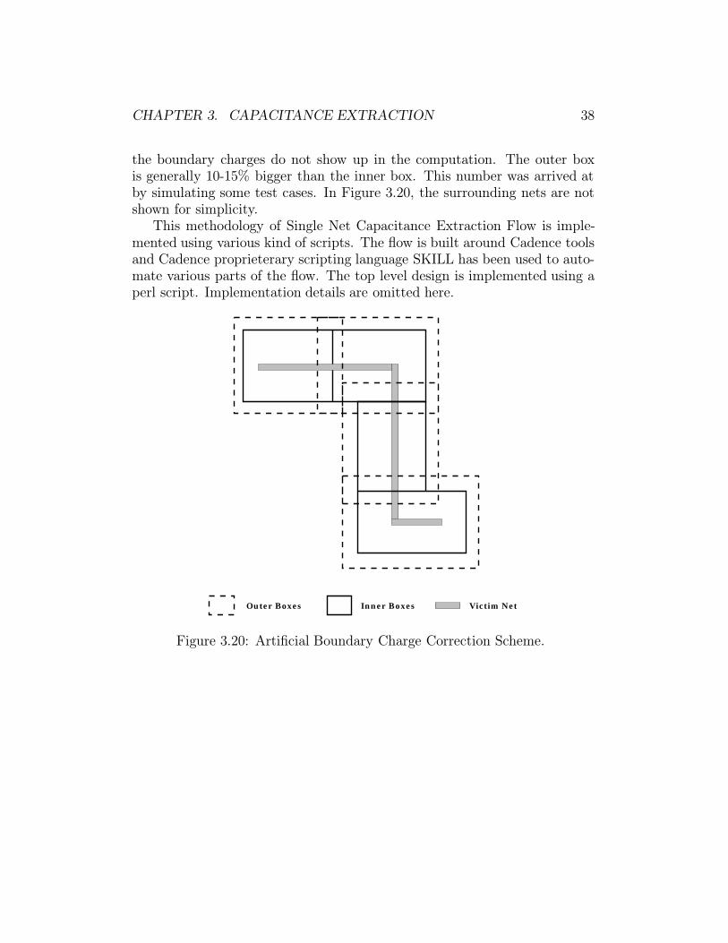
CHAPTER 3. CAPACITANCE EXTRACTION 38
the boundary charges do not show up in the computation. The outer boxis generally 10-15% bigger than the inner box. This number was arrived atby simulating some test cases. In Figure 3.20, the surrounding nets are notshown for simplicity.
This methodology of Single Net Capacitance Extraction Flow is imple-mented using various kind of scripts. The flow is built around Cadence toolsand Cadence proprieterary scripting language SKILL has been used to auto-mate various parts of the flow. The top level design is implemented using aperl script. Implementation details are omitted here.
Victim NetInner BoxesOuter Boxes
Figure 3.20: Artificial Boundary Charge Correction Scheme.

Chapter 4
Experimental Results
4.1 Introduction
The experimental characteristics of on-chip interconnects are of critical im-portance to high speed digital designers and to RF IC designers. In thischapter the experimental characterization of deep submicron interconnectsfabricated using Sematech’s Chemical Mechanical Polishing (CMP) processis discussed. Measurements are available for micron sized interconnects [26].This is in stark contrast to the enormous literature on numerical electro-magnetic modeling of interconnects. This situation is partly because of thesubstantial cost of fabricating chips with the sizable test structures required;the proprietary nature of deep submicron interconnect geometries and met-allurgy; and the measurement uncertainty issues. The measurement uncer-tainty issue is that there is no measurement procedure that will enable allthe four parameters (RLGC) to be independently extracted from microwavemeasurements alone.
4.2 Measurement Methodology
The essential modeling problem is that the effect of the on-chip fixturingneeds to be removed. The on-chip fixturing can have a significant effecton the measurement results and so calibration using standard calibrationsubstrates cannot be used. So, on-chip calibration structures are required forproper calibration.
The two port measurement procedure used here is the Through Line(TL) method [27]. This is an area efficient procedure requiring only two
39

CHAPTER 4. EXPERIMENTAL RESULTS 40
lengths of line with the shorter line designated as the through. The measure-ment procedure is outlined in Figure 4.1.
Automatic Network Analyzer
DeviceUnderTest
HP8510
1. Through Measurement:
2. Line Measurement:
Reference Planes
Mirowave Measurements:
(a)
(b)
(c)
Figure 4.1: Set-up for microwave measurements : (a) Test set-up usinga Cascade Microtech probe station, picoprobes from GGB industries andHewlett Packard Automatic Network Analyzer (ANA) HP8510C. Illustrationof Through Line (TL) calibration procedure : (b) Through measurement (c)Line measurement.
The TL method is similar in concept to the TRL (Through Reflect Line)procedure which uses a measurement with an arbitrary reflection appliedto each port (after the fixture). But, as discussed in Chapter 2 (literaturereview) TRL methods have certain drawbacks which are removed by TL pro-cedures. The TL method uses symmetry, or equivalently that the assumptionthat the two fixtures on port 1 and 2 are identical, to synthesize either anopen or a short at the reference plane. All that is required is that the net-work analyzer first be calibrated using an approximate Open Short Load(OSL) calibration to the ends of the probe tips on a standard calibration
CHAPTER 4. EXPERIMENTAL RESULTS 41
substrate. The symmetry requirements is that the fixture, the contact padsand breakaway, be accurately reproduced. This is also a requirement in allother calibration procedures and so no additional assumptions are imposed.
All measurement procedures requiring a through and a line require adetermination of the low frequency capacitance. Any of a number of tech-niques could be used [28, 29]. Here a 10 MHz LCR meter measurements areused. The details of the through-line calibration procedure is presented inthe literature review section of this report.
An important property of the TL measurement procedure is that the λ/2discontinuities that plague TRL do not occur. This is because the uncertaintyof the reflection standard is eliminated. In the TL procedure only two lengthsof lines are required. However, three lengths of lines were used so that twoexperimental characterizations could be obtained. In all the cases the twosets of measurements compared favorably with each other.
4.3 Measurement Setup
Transmission Line measurements were made using a Cascade Microtech probestation, picoprobes from GGB industries and a Hewlett Packard AutomaticNetwork Analyzer (ANA) HP8510C (see Figure 4.1). In Figure 4.1(a) twoprobes are shown each having three contacts: a signal contact and two groundcontacts. These three contacts end in three probe pads on the chip. Theprobe pads are 50 µm by 50 µm with the outer probe pads connected to thechip ground.
A Conventional capacitance measurement technique was used to measurethe capacitance. The GGB model 40 picoprobes were used which maintaina coaxial line to within 1 mm of the final test fingers. The guard contactsare extensions of the outer conductor of the coaxial line. Sub-picofarad ca-pacitance measurements require a balanced probe system, but the electricalbalance is disturbed at the probe, resulting in a residual capacitance. Theresidual capacitance of the microprobe and the probe pad is approximately70 fF. Capacitance measurements of two lines of different length but other-wise identical were done. The difference of the capacitances of these linesand the length difference were used to determine the capacitance per unitlength.
CHAPTER 4. EXPERIMENTAL RESULTS 42
4.4 Test Chip
The test chip was fabricated in the Sematech 0.1µ process with three metallayers : metal1 (the bottom layer), metal2 (the middle layer) and metal3(the top layer). The chip has metal lines in all the three layers with six dif-ferent widths viz., 0.25µm(V), 0.35µm(T), 0.45µm(S), 0.5µm(M), 0.6µm(X)and 0.7µm(W). Each of these lines are laid out in three different lengthsviz., 400µm(S), 800µm(M) and 6400µm(L). Two lines of different lengths areneeded to perform through-line (TL) measurements. Three different lengthsare drawn for verification purposes. All the lines are 0.5µm thick and thedistance between each metal layer as well as from metal1 layer to highlydoped epi layer is 1.0µm.
4.5 Comparison of Synthesized and Measured
Open Circuit in the Through Line Cali-
bration Technique
The inherent symmetry requirement in TL calibration permits synthesis ofTRL reflection standards. For the symmetrical through connection, we cansynthesize the reflection coefficient with the microstrip ports terminated inideal open or short circuits. On the test chip an open circuit was constructedand the measurement of this open circuit is compared to the synthesizedopen circuit. A similar comparison can also be done for a synthesized shortcircuit and measured short circuit. But, our experience is that a sufficientlygood short cannot be constructed because of via inductance and resistance.
4.5.1 Synthesis of Open Circuit Reflection Coefficient
The open circuit reflection coefficient can be synthesized using the measuredfixture S-parameters of a through. Here, a short line is considered as through.Three lines are chosen in three different metal layers with a width of 0.5µm.As a result of approximate OSL calibration the calibrated fixtures of the testsystem are identical so that in a through connection the embedded DUT(short metal line) is symmetrical.
Figure 4.2(a) shows the two port network with the through connection.It should be noted that because of the symmetry of the fixture ports A andB are identical. They are only named differently. Ports 1A and 1B were

CHAPTER 4. EXPERIMENTAL RESULTS 43
Port 1A Port 2A Port 1BA BPort 2B
(a)
S
S
S
S
CalibratedPort 1A Port 1B
Calibrated
12F
22F
21F
11F
(b)
Figure 4.2: Through connection in the Through Line calibration procedure:(a) network connection; and (b) signal flow graph with measured fixture Sparameters of the two port network.
calibrated in the tier 1 calibration (see literature review in Chapter 2) usingOSL calibration. Figure 4.2(b) shows the signal flow graph with the measuredfixture S-parameters with S11F = S22F and S12F = S21F .
The actual S parameters of the A or B network (Figure 4.2(a)) are δ,αand γ as shown in Figure 4.3. Consider the network in Figure 4.3(a). UsingMason’s rule and simplifying this signal flow graph to a form similar to thatin Figure 4.2(b), we obtain the following equalities:
S11F = δ +α2γ
1− γ2(4.1)
S21F =α2
1− γ2(4.2)
Now, consider the signal flow graph of the A network with the ideal opencircuit placed at fixture port 2A. Using Mason’s rule again, we calculate theopen circuit reflection coefficient as
ρoc = δ +α2
1− γ (4.3)
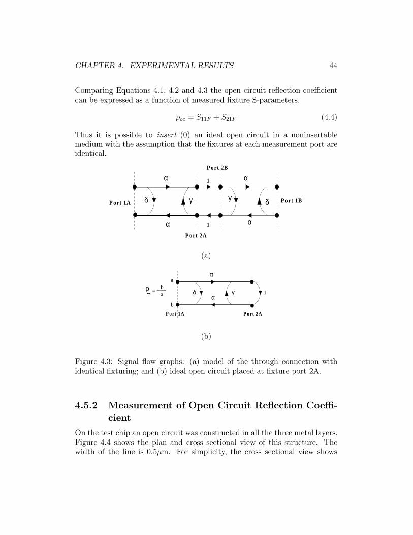
CHAPTER 4. EXPERIMENTAL RESULTS 44
Comparing Equations 4.1, 4.2 and 4.3 the open circuit reflection coefficientcan be expressed as a function of measured fixture S-parameters.
ρoc = S11F + S21F (4.4)
Thus it is possible to insert (0) an ideal open circuit in a noninsertablemedium with the assumption that the fixtures at each measurement port areidentical.
δ
α
γPort 1A
Port 2A
Port 2B
Port 1B
α
α
γ δ
α
1
1
(a)
αδ
α
γ 1
a
b
ρoc =
ba
Port 1A Port 2A
(b)
Figure 4.3: Signal flow graphs: (a) model of the through connection withidentical fixturing; and (b) ideal open circuit placed at fixture port 2A.
4.5.2 Measurement of Open Circuit Reflection Coeffi-cient
On the test chip an open circuit was constructed in all the three metal layers.Figure 4.4 shows the plan and cross sectional view of this structure. Thewidth of the line is 0.5µm. For simplicity, the cross sectional view shows
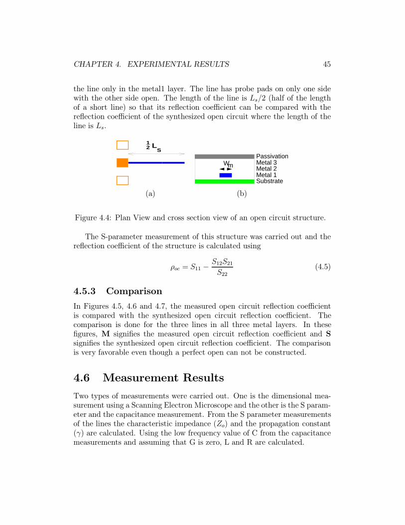
CHAPTER 4. EXPERIMENTAL RESULTS 45
the line only in the metal1 layer. The line has probe pads on only one sidewith the other side open. The length of the line is Ls/2 (half of the lengthof a short line) so that its reflection coefficient can be compared with thereflection coefficient of the synthesized open circuit where the length of theline is Ls.
LS
12
PassivationMetal 3Metal 2Metal 1Substrate
Wm
(a) (b)
Figure 4.4: Plan View and cross section view of an open circuit structure.
The S-parameter measurement of this structure was carried out and thereflection coefficient of the structure is calculated using
ρoc = S11 −S12S21
S22
(4.5)
4.5.3 Comparison
In Figures 4.5, 4.6 and 4.7, the measured open circuit reflection coefficientis compared with the synthesized open circuit reflection coefficient. Thecomparison is done for the three lines in all three metal layers. In thesefigures, M signifies the measured open circuit reflection coefficient and Ssignifies the synthesized open circuit reflection coefficient. The comparisonis very favorable even though a perfect open can not be constructed.
4.6 Measurement Results
Two types of measurements were carried out. One is the dimensional mea-surement using a Scanning Electron Microscope and the other is the S param-eter and the capacitance measurement. From the S parameter measurementsof the lines the characteristic impedance (Zo) and the propagation constant(γ) are calculated. Using the low frequency value of C from the capacitancemeasurements and assuming that G is zero, L and R are calculated.
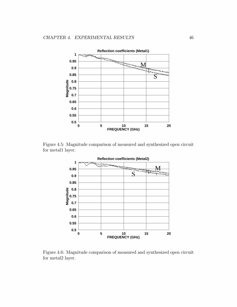
CHAPTER 4. EXPERIMENTAL RESULTS 46
0.5
0.55
0.6
0.65
0.7
0.75
0.8
0.85
0.9
0.95
1
0 5 10 15 20
Mag
nit
ud
e
FREQUENCY (GHz)
Reflection coefficients (Metal1)
M
S
Figure 4.5: Magnitude comparison of measured and synthesized open circuitfor metal1 layer.
0.5
0.55
0.6
0.65
0.7
0.75
0.8
0.85
0.9
0.95
1
0 5 10 15 20
Mag
nit
ud
e
FREQUENCY (GHz)
Reflection coefficients (Metal2)
MS
Figure 4.6: Magnitude comparison of measured and synthesized open circuitfor metal2 layer.

CHAPTER 4. EXPERIMENTAL RESULTS 47
0.5
0.55
0.6
0.65
0.7
0.75
0.8
0.85
0.9
0.95
1
0 5 10 15 20
Mag
nit
ud
e
FREQUENCY (GHz)
Reflection coefficients (Metal3)
MS
Figure 4.7: Magnitude comparison of measured and synthesized open circuitfor metal3 layer.
h
t_Alt_TiTu
Wbot
WtopMetal1
DIELECTRIC(SiO2)
AIR
EPI LAYER
SUBSTRATE
d
Figure 4.8: Line diagram of a metal line (in metal1 layer). The TiTu(titanium-tungsten) layer was deposited and then plated with aluminum.

CHAPTER 4. EXPERIMENTAL RESULTS 48
4.6.1 Dimensional Measurement
Scanning Electron Microscope (SEM) is used to obtain cross-section imagesof all the structures. These images are used to draw the line diagram of aline over a ground plane (highly doped epi layer) (see Figure 4.8).
Figure 4.9 shows SEM images of two metal lines. Figure 4.9(a) shows ametal1 line and Figure 4.9(b) shows a metal3 line. Both the lines in Figure 4.9have drawn lengths of 0.5µm. The SEM images show that the lines havetrapezoidal cross section. Before depositing metal a thin layer of titanium-tungsten layer is deposited. This is shown in Figure 4.8.
Using the SEM images various dimensions of the lines were measured.The measured dimensions along with the drawn dimensions are tabulated inTable 4.1. The symbols in the table refers to Figure 4.8. It can be seen fromthe Table 4.1 that the average width of the lines are not the same as thedrawn width because of process variations.

CHAPTER 4. EXPERIMENTAL RESULTS 49
(a)
(b)
Figure 4.9: Scanning Electron Micrograph of the cross-section of a line in (a)metal1; and (b) metal3 layers.
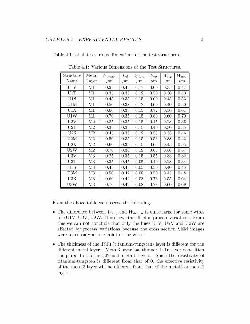
CHAPTER 4. EXPERIMENTAL RESULTS 50
Table 4.1 tabulates various dimensions of the test structures.
Table 4.1: Various Dimensions of the Test Structures.
Structure Metal Wdrawn tAl tT iTu Wbot Wtop Wavg
Name Layer µm µm µm µm µm µm
U1V M1 0.25 0.45 0.17 0.60 0.35 0.47
U1T M1 0.35 0.38 0.12 0.50 0.30 0.40
U1S M1 0.45 0.35 0.15 0.60 0.45 0.53
U1M M1 0.50 0.38 0.12 0.60 0.40 0.50
U1X M1 0.60 0.35 0.15 0.72 0.50 0.61
U1W M1 0.70 0.35 0.15 0.80 0.60 0.70
U2V M2 0.25 0.35 0.15 0.45 0.28 0.36
U2T M2 0.35 0.35 0.15 0.40 0.30 0.35
U2S M2 0.45 0.38 0.12 0.55 0.38 0.46
U2M M2 0.50 0.35 0.15 0.53 0.38 0.42
U2X M2 0.60 0.35 0.15 0.65 0.45 0.55
U2W M2 0.70 0.38 0.12 0.65 0.50 0.57
U3V M3 0.25 0.35 0.15 0.55 0.33 0.32
U3T M3 0.35 0.45 0.05 0.40 0.28 0.34
U3S M3 0.45 0.45 0.05 0.50 0.40 0.45
U3M M3 0.50 0.42 0.08 0.50 0.45 0.48
U3X M3 0.60 0.42 0.08 0.73 0.55 0.64
U3W M3 0.70 0.42 0.08 0.78 0.60 0.69
From the above table we observe the following.
• The difference between Wavg and Wdrawn is quite large for some wireslike U1V, U2V, U2W. This shows the effect of process variations. Fromthis we can not conclude that only the lines U1V, U2V and U2W areaffected by process variations because the cross section SEM imageswere taken only at one point of the wires.
• The thickness of the TiTu (titanium-tungsten) layer is different for thedifferent metal layers. Metal3 layer has thinner TiTu layer depositioncompared to the metal2 and metal1 layers. Since the resistivity oftitanium-tungsten is different from that of 0, the effective resistivityof the metal3 layer will be different from that of the metal2 or metal1layers.

CHAPTER 4. EXPERIMENTAL RESULTS 51
4.6.2 S Parameters and Capacitance Measurements
For the structures in Table 4.1 S parameters and capacitance measurementswere carried out. The measurements are described and results are presentedfor one of the test structure in [30].
Capacitance measurements were done using an LCR meter (HP 4275)at 10 MHz. These measurements are tabulated in Table 4.2. The resultobtained by measurements are also modeled using FastCap with the toolLayout2FastCap described in the previous chapter. Using 0, capacitance wasfound for lines of two different lengths viz., 5µm and 10µm. The capacitanceper unit length is found by taking the difference of the capacitance of theabove two lines and dividing by 5µm (difference in the length of the twolines). Comparing the simulation results with the measurement results itwas found that the lines in metal3 have a good match. Percentage differencein capacitance was found using the following expression.
Cdiff =|CFastCap − C10MHz|
(CFastCap + C10MHz)/2× 100% (4.6)
Using a multimeter, the DC resistance of the structures were also measuredand these are tabulated in Table 4.2.
S parameter measurements were done using the setup shown in Figure 4.1.From the S-parameters measurements the propagation constant and the char-acteristic impedances of the lines are calculated. Propagation constant andcharacteristic impedance at 10 GHz are tabulated in Table 4.3. Using thevalue of C10MHz from Table 4.2 and G = 0, the frequency dependence ofresistances and inductances are derived. The values of resistances and induc-tances extracted at 10 GHz are tabulated in Table 4.3.
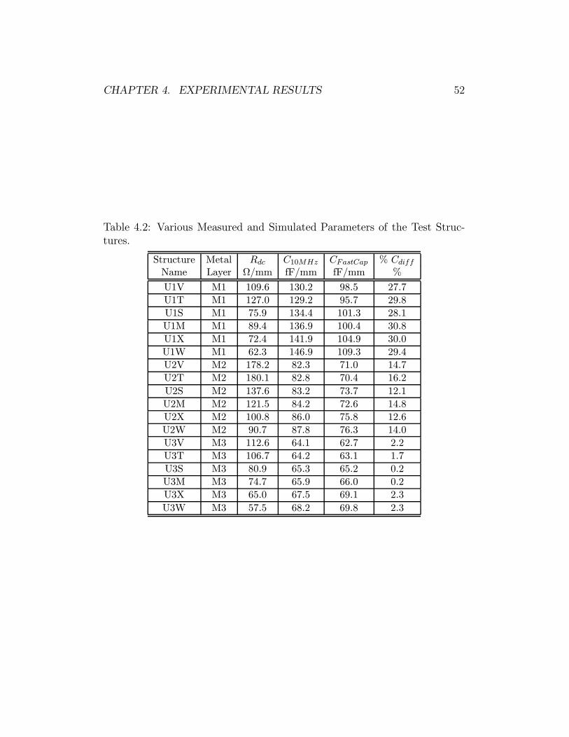
CHAPTER 4. EXPERIMENTAL RESULTS 52
Table 4.2: Various Measured and Simulated Parameters of the Test Struc-tures.
Structure Metal Rdc C10MHz CFastCap % CdiffName Layer Ω/mm fF/mm fF/mm %
U1V M1 109.6 130.2 98.5 27.7
U1T M1 127.0 129.2 95.7 29.8
U1S M1 75.9 134.4 101.3 28.1
U1M M1 89.4 136.9 100.4 30.8
U1X M1 72.4 141.9 104.9 30.0
U1W M1 62.3 146.9 109.3 29.4
U2V M2 178.2 82.3 71.0 14.7
U2T M2 180.1 82.8 70.4 16.2
U2S M2 137.6 83.2 73.7 12.1
U2M M2 121.5 84.2 72.6 14.8
U2X M2 100.8 86.0 75.8 12.6
U2W M2 90.7 87.8 76.3 14.0
U3V M3 112.6 64.1 62.7 2.2
U3T M3 106.7 64.2 63.1 1.7
U3S M3 80.9 65.3 65.2 0.2
U3M M3 74.7 65.9 66.0 0.2
U3X M3 65.0 67.5 69.1 2.3
U3W M3 57.5 68.2 69.8 2.3

CHAPTER 4. EXPERIMENTAL RESULTS 53
Table 4.3: Various Derived Parameters of the Test Structures.
Structure Metal γ(10GHz) Zo(10GHz) R(10 GHz) L(10 GHz)Name Layer 1/m Ω kΩ/m nH/m
U1V M1 997.5 6 66.6 121.7 6 -23.4 88.4 1320.5
U1T M1 1023.9 6 58.9 125.9 6 -31.0 114.0 956.2
U1S M1 1013.0 6 59.3 119.7 6 -30.7 106.5 920.3
U1M M1 999.9 6 59.8 116.0 6 -30.2 100.8 911.1
U1X M1 952.5 6 57.7 106.6 6 -32.3 91.7 692.1
U1W M1 901.8 6 61.7 97.5 6 -28.3 73.4 767.1
U2V M2 923.6 6 55.7 178.3 6 -34.3 153.3 953.6
U2T M2 940.6 6 55.4 180.4 6 -34.5 158.5 961.0
U2S M2 845.1 6 58.1 161.3 6 -31.9 122.3 958.6
U2M M2 794.5 6 59.5 149.9 6 -30.5 104.1 919.3
U2X M2 755.1 6 62.0 139.5 6 -28.0 87.3 937.4
U2W M2 712.8 6 66.9 129.0 6 -23.1 66.4 1010.2
U3V M3 693.7 6 58.0 171.8 6 -32.0 107.2 828.0
U3T M3 678.4 6 58.6 167.7 6 -31.4 101.2 826.9
U3S M3 617.3 6 64.8 150.2 6 -25.2 71.4 938.9
U3M M3 613.1 6 64.9 147.9 6 -25.0 69.6 923.2
U3X M3 587.0 6 64.1 138.1 6 -25.9 63.6 798.0
U3W M3 569.9 6 65.1 132.6 6 -24.9 57.8 773.9

Chapter 5
Conclusion
5.1 Conclusions
A three dimensional interconnect modeling software (Layout2FastCap) wasdeveloped that takes a Layout (CIF) as its input and generates panel files thatare analyzed by FastCap to generate a capacitance matrix. Various issuesrelated to the three dimensional modeling of interconnects were investigatedand the solutions were implemented in the Layout2FastCap software.
A new technique of simulating the ground plane using image method wasalso explored. The method is generalized for a system with n conductors andan infinite ground plane. The result is a simple transformation that convertsthe 2n × 2n capacitance matrix of a system with n conductors and theirimages (2n conductors) to a n × n capacitance matrix of a system with nconductors and an infinite ground plane.
The limitation of Layout2FastCap is that it can handle only a relativelysmall layout. A flow (Single Net Capacitance Extraction flow) was developedto solve this problem. The idea behind this approach is dividing the originallayout into several small manageable parts that can be 1 by Layout2FastCap.A boundary error correction scheme is implemented to take care of the ac-cumulation of artificial charges at the boundary of the conductors.
Capacitance and transmission line measurements were analyzed and theresults compared with the simulation results. A close match was found be-tween the capacitance measurements of the test structures in metal3 layerwith the simulation results of Layout2FastCap.
54

CHAPTER 5. CONCLUSION 55
5.2 Future Research
There are a number of ways in which present work can be expanded. Themeasurement results along with the simulation results from FastCap can beused to develop analytical models for interconnect capacitance. This wouldrequire measurements of smaller capacitance structures using Atomic forceCapacitance Meter (ACM), along with those reported here.
The software Layout2FastCap can also be improved in several ways. Atpresent, Layout2FastCap can model interconnects, with trapezoidal cross-section only for the conductors which do not have any bends. This limi-tation can be removed by developing an algorithm that handle bends withtrapezoidal cross-section. Also, at present Layout2FastCap can model only auniform dielectric medium. It can be enhanced to handle multiple dielectriclayers. Only a stratified dielectric structure needs to be modeled as most pro-cesses use chemical mechanical polishing for planarization. In this case, thedielectric interface needs to be discretized like the surfaces of the conductors.This is because charges will accumulate at the dielectric interface.

Bibliography
[1] The National Technology Roadmap for Semiconductors, SemiconductorIndustry Association, 4300 Stevens Creek Blvd., Suite 271, San Jose,CA 95129, 1994.
[2] S. Y. Oh and K. J. Chang, “2001 Needs for Multi-Level InterconnectTechnology,” Circuits and Devices Magazine, Vol. 11, January 1995, pp.16-21.
[3] P. Felix, “Interconnects for ULSI: State of the art and Future Trends,”Proceedings of the ESSDERC, 1995 pp. 5-14.
[4] H. B. Bakoglu, Circuits, Interconnections and Packaging for VLSI,Addison-Wesley Publishing Co., Reading, MA, 1990.
[5] A. K. Goel, High Speed VLSI Interconnects: Modeling Analysis andSimulation, John Wiley & Sons, Inc., 1994.
[6] C. W. Koburger III et. al., “A Half-Micron CMOS Logic Generation,”IBM Journal of Research and Development, Vol. 39, 1995, pp. 215.
[7] S. P. Jeng, K. Taylor, T. Seha, M. C. Chang, J. Fattaruso andR. H. Havemann, “Highly Porous Interlayer Dielectric for Intercon-nect Capacitance Reduction,” Digest of Technical Papers Symposiumon VLSI Technology, 1995, pp. 61-62.
[8] B. Luther et. al., “Planar Copper Polymide Back End of the Line In-terconnections for ULSI Devices,” Proceedings of the 10th InternationalVLSI Multilevel Interconnection Conference, 1993, pp. 15.
[9] E. A. Dengi and R. A. Rohrer, “Hierarchical 2-D Field Solution forCapacitance Extraction for VLSI Interconnect Modeling,” ProceedingsDesign Automation Conference, 1997, pp. 127-132.
56
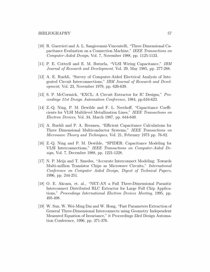
BIBLIOGRAPHY 57
[10] R. Guerrieri and A. L. Sangiovanni-Vincentelli, “Three Dimensional Ca-pacitance Evaluation on a Connection Machine,” IEEE Transactions onComputer-Aided Design, Vol. 7, November 1988, pp. 1125-1133.
[11] P. E. Cottrell and E. M. Buturla, “VLSI Wiring Capacitance,” IBMJournal of Research and Development, Vol. 29, May 1985, pp. 277-288.
[12] A. E. Ruehli, “Survey of Computer-Aided Electrical Analysis of Inte-grated Circuit Interconnections,” IBM Journal of Research and Devel-opment, Vol. 23, November 1979, pp. 626-639.
[13] S. P. McCormick, “EXCL: A Circuit Extractor for IC Designs,” Pro-ceedings 21st Design Automation Conference, 1984, pp.616-623.
[14] Z.-Q. Ning, P. M. Dewilde and F. L. Neerhoff, “Capacitance Coeffi-cients for VLSI Multilevel Metallization Lines,” IEEE Transactions onElectron Devices, Vol. 34, March 1987, pp. 644-649.
[15] A. Ruehli and P. A. Brennen, “Efficient Capacitance Calculations forThree Dimensional Multiconductor Systems,” IEEE Transactions onMicrowave Theory and Techniques, Vol. 21, February 1973 pp. 76-82.
[16] Z.-Q. Ning and P. M. Dewilde, “SPIDER: Capacitance Modeling forVLSI Interconnections,” IEEE Transactions on Computer-Aided De-sign, Vol. 7, December 1988, pp. 1221-1228.
[17] N. P. Meijs and T. Smedes, “Accurate Interconnect Modeling: TowardsMulti-million Transistor Chips as Microwave Circuits,” InternationalConference on Computer Aided Design, Digest of Technical Papers,1996, pp. 244-251.
[18] O. E. Akcasu, et. al., “NET-AN a Full Three-Dimensional ParasiticInterconnect Distributed RLC Extractor for Large Full Chip Applica-tions,” Proceedings International Electron Devices Meeting, 1995, pp.495-498.
[19] W. Sun, W. Wei-Ming Dai and W. Hong, “Fast Parameters Extraction ofGeneral Three-Dimensional Interconnects using Geometry IndependentMeasured Equation of Invariance,” it Proceedings 33rd Design Automa-tion Conference, 1996, pp. 371-376.

BIBLIOGRAPHY 58
[20] K. Nabros and J. White, “FastCap: A Multipole Accelerated 3-D Ca-pacitance Extraction Program,” IEEE Transactions on Computer-AidedDesign, Vol. 10, November 1991, pp. 1447-1459.
[21] K. Nabros, S. Kim and J. White, “Fast Capacitance Extraction of Gen-eral Three-Dimensional Structures,” IEEE Transactions on MicrowaveTheory and Techniques, Vol. 40, July 1992, pp. 1496-1506.
[22] FastCap User’s Guide, J. White, Research Laboratory of Electron-ics, Department of Electrical Engineering and Computer Science, Mas-sachusetts Institute of Technology, Cambridge, MA 02139.
[23] Raphael Interconnect Analysis User’s Manual, Technology Modeling As-sosciates, Inc. Third Floor, 300 Hamilton Avenue, Palo Alto, CA 94301.
[24] C. Mead and L. Conway, Introduction to VLSI Systems, Addison-WesleyPublishing Co., Reading, MA, 1980, pp. 115-127.
[25] D. J. Griffiths, Introduction to Electrodynamics, Prentice-Hall, 1989, pp.121-125.
[26] A. Deutsch, G. V. Kopcsay, C. W. Surovic, B. J. Rubin, L. M. Terman,R. P. Dunne Jr., T. A. Gallo, and R. H. Dennard, “Modeling and Char-acterization of Long On-Chip Interconnections for High-PerformanceMicroprocessors,” IBM Journal of Research and Development, Vol. 39,September 1995, pp. 547-567.
[27] M. B. Steer, S. B. Goldberg, G. Rinne, P. D. Franzon, I. Turlik andJ. S. Kasten, “Introducing the Through-Line Deembedding Procedure,”1992 IEEE MTT-S International Microwave Symposium Digest, June1992, pp. 1455-1458.
[28] S. Lipa, M. B. Steer, A. S. Morris, and P. D. Franzon, “Comparisonof Methods for Determining the Capacitance of Planar TransmissionLines with Application to Multichip Module Characterization,” IEEETrans. on Components Hybrids and Manufacturing Technology, Part B:Advanced Packaging, Vol. 16, May 1993, pp. 247-252.
[29] S. Lipa, M. B. Steer, A. C. Cangellaris and P. D. Franzon, “Experi-mental Characterization of Transmission Lines in Thin-Film MultichipModules,” IEEE Trans. on Components, Packaging, and ManufacturingTechnology — Part A, Vol. 19, March 1996, pp. 122-126.

BIBLIOGRAPHY 59
[30] B. Biswas, A. W. Glaser, S. Lipa, M. B. Steer, P. D. Franzon, D. Griffis,and P. Russell, “Experimental Electrical Characterization of On-ChipInterconnects,” Electrical Performance of Electronic Packaging, October1997, pp. 57-59.
[31] B. W. McGaughy, J. C. Chen, D. Sylvester and C. Hu, “A SimpleMethod for On-Chip, Sub-Femto Farad Interconnect Capacitance Mea-surement,” IEEE Electron Devices Letters, January 1997, pp. 21-23.
[32] P. Nouet and A. Toulouse, “Test Chip for Interconnect CapacitanceModeling in a CMOS Process,” IEEE International Conference on Mi-croelectronic Test Structures, 1996, pp. 61-65.
[33] M. B. Steer, S. B. Goldberg and P. D. Franzon, “Comment on an Accu-rate Measurement Technique for Line Properties, Junction Effects andDielectric and Magnetic Parameters,” IEEE Transactions MicrowaveTheory and Techniques, Vol. 39, February 1992, pp. 410-411.

Appendix A
Caltech Intermediate Format
The Caltech Intermediate Format (CIF) is a means of describing graphicitems (mask features). Its purpose is to serve as a standard machine-readablerepresentation of the layout of an integrated circuit. The file generated usingthis format is a fairly readable text file. CIF files are usually created bycomputer programs from other representations, such as a symbolic layoutlanguage or an interactive design program. The basic idea of the format isto specify every geometric object in the design using ample precision.
A.1 Syntax
A CIF file is composed of a sequence of characters in a limited characterset. The file contains a list of commands, followed by an end marker; thecommands are separated with semicolons. A formal definition of the syntaxis given below.
cifFile = blank [command] semi endcommandblank.
command = primCommand | defDeleteCommand |defStartCommand semi blank[primCommand] semi defFinishCommand.
primCommand = polygonCommand | boxCommand |roundFlashCommand | wireCommand |
layerCommand | callCommand |userExtensionCommand | commentCommand.
polygonCommand = "P" path.
60

APPENDIX A. CALTECH INTERMEDIATE FORMAT 61
boxCommand = "B" integer sep integer sep point[sep point].
roundFlashCommand = "R" integer sep point.wireCommand = "W" integer sep path.layerCommand = "L" blank shortname.
defStartCommand = "D" blank "S" integer [sep integersep integer].
defFinishCommand = "D" blank "F".defDeleteCommand = "D" blank "D" integer.callCommand = "C" integer transformation.userExtensionCommand = digit userText.commentCommand = "(" commentText ")".endcommand = "E".transformation = blank ("T" point | "M" blank "X" |
"M" blank "Y" | "R" point) .path = point sep point.point = sInteger sep sInteger.sInteger = sep ["-"] integerD.integer = sep integerD.integerD = digit digit.shortname = c [c] [c] [c].c = digit | upperChar.
userText = userChar.commentText = commentChar | commentText "("
commentText ")" commentText.semi = blank ";" blank.sep = upperChar | blank.digit = "0" | "1" | "2" | "3" | ... | "8" | "9".upperChar = "A" | "B" | "C" | "D" | ... | "Y" | "Z".blank = any ascii character except digit, upperChar,
"-", "(", ")" or ";".
userChar = any ascii character except ";".commentCahr = any ascii character except "(" or ")".
The fundamental idea of the intermediate form is to describe unambigu-ously the geometry of patterns in a mask level layout. Many of the decisionsin designing the file format were made to avoid ambiguity: floating pointnumbers are avoided and there are no iterative constructs.

APPENDIX A. CALTECH INTERMEDIATE FORMAT 62
A simple file format might include only primitive geometric constructs,such as polygons, boxes, flashes and wires. Unfortunately, the geometricdescription of a chip with hundreds of thousands of rectangles on it wouldrequire an immense file of this sort. Hence, a provision has been made fordefining and calling symbols which reduces the size of the files substantially.
Appendix B
Layout2FastCap
B.1 Input Files
Layout2FastCap uses three input files to generate the panel files as describedin Chapter 3. The input files are
• CIF File. The details of the caltech intermediate format is describedin Appendix A.
• Process Data File. This contains the process information for a partic-ular technology. Layout2FastCap uses this file to generate the threedimensional structures from the two dimensional structures.
• Layer Mapping File. This maps the internal layer names in Lay-out2FastCap to the names used in CIF file.
In this appendix only the Process Data File and the Layer Mapping Filewill be described.
63
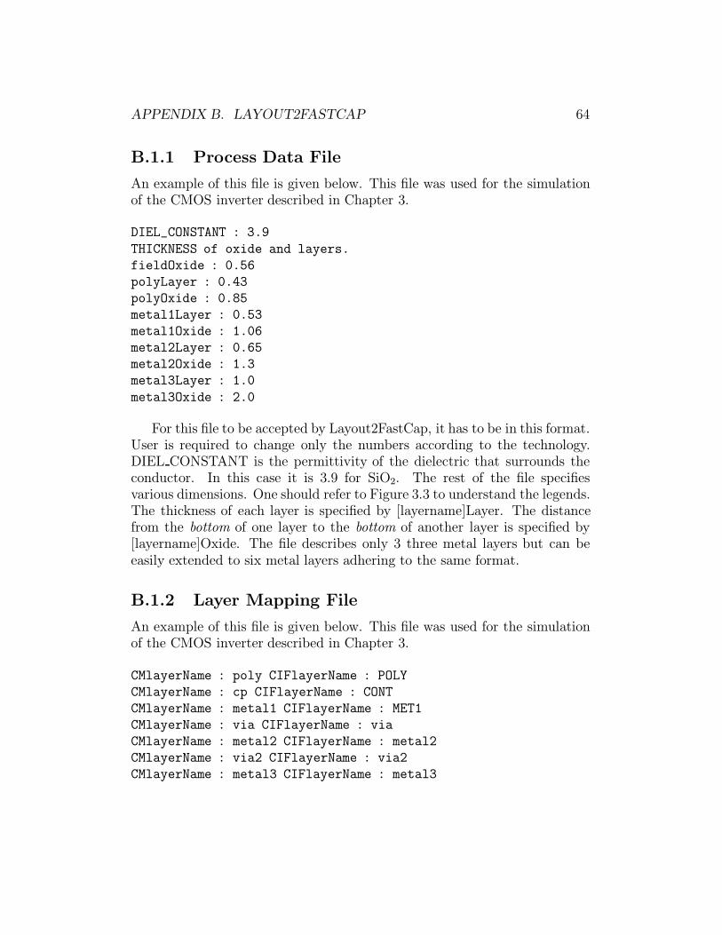
APPENDIX B. LAYOUT2FASTCAP 64
B.1.1 Process Data File
An example of this file is given below. This file was used for the simulationof the CMOS inverter described in Chapter 3.
DIEL_CONSTANT : 3.9
THICKNESS of oxide and layers.fieldOxide : 0.56polyLayer : 0.43polyOxide : 0.85metal1Layer : 0.53metal1Oxide : 1.06metal2Layer : 0.65metal2Oxide : 1.3metal3Layer : 1.0
metal3Oxide : 2.0
For this file to be accepted by Layout2FastCap, it has to be in this format.User is required to change only the numbers according to the technology.DIEL CONSTANT is the permittivity of the dielectric that surrounds theconductor. In this case it is 3.9 for SiO2. The rest of the file specifiesvarious dimensions. One should refer to Figure 3.3 to understand the legends.The thickness of each layer is specified by [layername]Layer. The distancefrom the bottom of one layer to the bottom of another layer is specified by[layername]Oxide. The file describes only 3 three metal layers but can beeasily extended to six metal layers adhering to the same format.
B.1.2 Layer Mapping File
An example of this file is given below. This file was used for the simulationof the CMOS inverter described in Chapter 3.
CMlayerName : poly CIFlayerName : POLYCMlayerName : cp CIFlayerName : CONTCMlayerName : metal1 CIFlayerName : MET1CMlayerName : via CIFlayerName : viaCMlayerName : metal2 CIFlayerName : metal2CMlayerName : via2 CIFlayerName : via2CMlayerName : metal3 CIFlayerName : metal3

APPENDIX B. LAYOUT2FASTCAP 65
Here, CMlayerName are the layer names that are used internally by Lay-out2FastCap and CIFlayerName are the corresponding layer names in theCIF file. The internal layer names (CMlayerName) remains the same al-ways, the user has to change only the CIFlayerName. By using this fileLayout2FastCap is independent of the various naming conventions in thetechnology file.
B.2 Program Implementation
In this section the implementation details of Layout2FastCap are discussed.
B.2.1 Source Files
In this section a brief description of all the source files of Layout2FastCap isgiven.
• CIF parser files.
1. cif parser.lex. This is the lexical analyzer file that parses theinput CIF file and returns tokens to the yacc file.
2. cif parser.y. This is the grammar file that gets tokens from thelex file. If the input CIF file doesn’t obey the grammar it flags anerror, otherwise it stores the information in the data structures.
• Header files.
1. global.h. This header file has the declarations and definitions ofvarious data structures and procedures. It also declares the globalvariables.
2. def.h. This header file defines certain variables that control theexecution of Layout2FastCap.
• .c files.
1. main.c. This is the main C program which calls the parser andthe procedure fcRectGen in fcRectGen.c.
2. fcRectGen.c. This takes as its input the list of polygons, wiresand boxes and generates the meshed interconnects using variousprocedures from other files.

APPENDIX B. LAYOUT2FASTCAP 66
3. fcUtils.c. This file contains miscellaneous procedures that areused by fcRectGen.c. It has procedures to read the layer mappingand process data file, classify rectangles based on layer names andassociate label names with conductors. It also has main proce-dures for generating rectangles from wire and polygons and gen-erating inter and intra layer connectivity.
4. pgon.c. This has the procedure that generates rectangles fromthe polygons.
5. wire.c. This has the procedure that generates rectangles from thewires.
6. fcPrint.c. This has procedures for printing the contents of variouslists. This is for debugging purposes.
7. findOverlap.c. This has procedures that generates inter andintra layer connectivity.
8. newRectGen.c. This has the procedure that generates new rect-angles when two rectangles overlap in the same layer.
9. discretize.c. This generates the three dimensional structure ofthe interconnects and discretizes the surfaces.
10. panelSize.c. This has the procedure that generates the panelsizes for discretize.c.
B.2.2 Makefile
In this section, the makefile for Layout2FastCap is described.
# Makefile for the Layout to FastCap input# translator (Layout2FastCap)## C compilerCC = gcc -g# lex (flex)LEX = /ncsu/gnu/bin/flex
# yacc (bison)YACC = /ncsu/gnu/bin/bison# linker flags, for flex and math libraryLDFLAGS= -lfl -lm#

APPENDIX B. LAYOUT2FASTCAP 67
# object filesOBJS = cif_parser.tab.o lex.yy.o main.o fcRectGen.ofcUtils.o pgon.o wire.o fcPrint.o findOverlap.onewRectGen.o discretize.o panelSize.o#
# *Explicit Rules*.PHONY: clean dep allall: Layout2FastCapLayout2FastCap: $(OBJS)
$(CC) $(OBJS) -o Layout2FastCap $(LDFLAGS)cif_parser.tab.h: cif_parser.tab.c cif_parser.ycif_parser.tab.c: cif_parser.y
$(YACC) -dt cif_parser.ylex.yy.c: cif_parser.lex
$(LEX) cif_parser.lexclean:
-rm *.o *.tab.[ch] lex.yy.c .depend.depend: cif_parser.tab.c lex.yy.c
$(CC) -M $(OBJS:.o=.c) > .depend#include .depend
It uses the gnu C compiler, gnu lex (flex) and gnu yacc (bison). Beforethe make is done, it should be ensured that the above executables are in thepath.