modeling, analysis and mitigation of sub-synchronous
TRANSCRIPT

University of Alberta
Modeling, Analysis and Mitigation of Sub-SynchronousInteractions between Full- and Partial-Scale
Voltage-Source Converters and Power Networks
by
Khaled Mohammad Alawasa
A thesis submitted to the Faculty of Graduate Studies and Research in partialfulfillment of the requirements for the degree of
Doctor of Philosophy
in
Power Engineering and Power Electronics
Department of Electrical & Computer Engineering
c©Khaled Mohammad AlawasaSpring 2014
Edmonton, Alberta
Permission is hereby granted to the University of Alberta Libraries to reproduce single
copies of this thesis and to lend or sell such copies for private, scholarly or scientific
research purposes only. Where the thesis is converted to, or otherwise made available
in digital form, the University of Alberta will advise potential users of the thesis of
these terms.
The author reserves all other publication and other rights in association with the
copyright in the thesis and, except as herein before provided, neither the thesis nor any
substantial portion thereof may be printed or otherwise reproduced in any material
form whatsoever without the author’s prior written permission.

Abstract
Voltage-source converters (VSCs) have gained widespread acceptance in modern
power systems. The stability and dynamics of power systems involving these de-
vices have recently become salient issues. In the small-signal sense, the dynamics
of VSC-based systems is dictated by its incremental output impedance, which is
formed by a combination of ‘passive’ circuit components and ‘active’ control el-
ements. Control elements such as control parameters, control loops, and control
topologies play a significant role in shaping the impedance profile. Depending on
the control schemes and strategies used, VSC-based systems can exhibit differ-
ent incremental impedance dynamics. As the control elements and dynamics are
involved in the impedance structure, the frequency-dependent output impedance
might have a negative real-part (i.e., a negative resistance). In the grid-connected
mode, the negative resistance degrades the system damping and negatively impacts
the stability. In high-voltage networks where high-power VSC-based systems are
usually employed and where sub-synchronous dynamics usually exist, integrating
large VSC-based systems might reduce the overall damping and results in unstable
dynamics.
The objectives of this thesis are to (1) investigate and analyze the output
impedance properties under different control strategies and control functions, (2)
identify and characterize the key contributors to the impedance and sub-synchronous
damping profiles, and (3) propose mitigation techniques to minimize and eliminate
the negative impact associated with integrating VSC-based systems into power sys-
tems. Different VSC configurations are considered in this thesis; in particular, the

full-scale and partial-scale topologies (doubly fed-induction generators) are ad-
dressed. Additionally, the impedance and system damping profiles are studied
under two different control strategies: the standard vector control strategy and
the recently-developed power synchronization control strategy. Furthermore, this
thesis proposes a simple and robust technique for damping the sub-synchronous
resonance in a power system with series-compensated line by using the impedance
reshaping approach

Acknowledgements
First and foremost I would like to express my wholehearted gratitude to Allah,
the Almighty, for enlightening my path and guiding me through each and every
success I have or may reach.
I would like to thank and express my deep appreciation and sincere gratitude to
my supervisor Prof. Yasser A.-R. I. Mohamed, for his inspiring guidance, invalu-
able discussions, continuous encouragement and endless support throughout this
research. It has been an honor and privilege to work under his supervision. His
enthusiasm and attitude are respected and will never be forgotten. Also I would
like to thank my co-supervisor Prof. Wilsun Xu, for his support.
I gratefully acknowledge Mu’tah University, Jordan, for the scholarship and the
financial support provided for this research.
I would like to express my thanks to the examiners committee, Dr. A. Yazdani,
Dr. S. Ali Khajehoddin and Dr. J. Salmon for their valued comments and interests
in my thesis.
I am forever indebted to my parents for all their endless patience, encourage-
ment, prayers and love for my entire life. I owe my deepest gratitude to my beloved
wife, Hend. Without her endless encouragement, support, patience and love, this
work would have never been completed.
Lastly, I would also like to express my gratitude to the love, prayers and support
from my sisters, brothers, aunts and uncles, parents-in-law, teachers and professors,
friends and colleagues.

Contents
1 Introduction 1
1.1 Problem Statement and Research Motivation . . . . . . . . . . . . . 1
1.2 Review of Previous Work . . . . . . . . . . . . . . . . . . . . . . . . 2
1.2.1 Sub-Synchronous Interaction Analysis . . . . . . . . . . . . . 2
1.2.2 Impedance Modeling of Voltage-Source Converters (VSCs) . 4
1.2.3 Sub-Synchronous Interaction between VSCs and Networks . 5
1.2.4 Mitigation of Sub-synchronous Resonance (SSR) . . . . . . . 6
1.2.5 Power Synchronization VSC-based Interaction . . . . . . . . 7
1.2.6 Output Impedance of a Doubly Fed-Induction Generator and
Networks Interaction . . . . . . . . . . . . . . . . . . . . . . 8
1.3 Research Objectives . . . . . . . . . . . . . . . . . . . . . . . . . . 9
1.4 Thesis Contribution and Outline . . . . . . . . . . . . . . . . . . . . 10
2 Derivation and Analysis of the VSC Output Impedance 12
2.1 Definition of the Impedance of VSC . . . . . . . . . . . . . . . . . . 12
2.2 Output Impedance with Inner Current Controller . . . . . . . . . . 13
2.3 Output Impedance with Phase-Locked Loop (PLL) Dynamics . . . 16
2.4 Output Impedance with Outer Loops (Active Component) . . . . . 19
2.4.1 DC-Link Voltage Control . . . . . . . . . . . . . . . . . . . . 19
2.4.2 Active Power Control . . . . . . . . . . . . . . . . . . . . . . 21
2.5 Output Impedance with Outer Loops (Quadrature Component) . . 22
2.5.1 AC Voltage Control Mode . . . . . . . . . . . . . . . . . . . 22
2.5.2 Reactive Power Control Mode . . . . . . . . . . . . . . . . . 23
2.5.3 Unity Power Factor Controller . . . . . . . . . . . . . . . . . 23
2.6 Overall Impedance Model . . . . . . . . . . . . . . . . . . . . . . . 24
2.7 Controller Design Criteria . . . . . . . . . . . . . . . . . . . . . . . 24
3 Impedance Analysis and Dynamic Interaction Assessments 29
3.1 Electrical Damping Analysis Methods . . . . . . . . . . . . . . . . . 29

3.2 System Modeling (Network and Synchronous Machine Models) . . . 31
3.3 IEEE FBM Torsional Analysis . . . . . . . . . . . . . . . . . . . . . 32
3.4 Analysis of Output Impedance of VSC . . . . . . . . . . . . . . . . 32
3.4.1 Analysis of the Internal Impedance . . . . . . . . . . . . . . 32
3.4.2 Output Impedance with All Loop Components . . . . . . . 34
3.4.3 Impact of Phase-Locked Loop (PLL) Dynamics . . . . . . . 35
3.4.4 Impact of AC-Voltage Control Loop . . . . . . . . . . . . . 36
3.5 Sensitivity Studies and Electrical Damping Analyses . . . . . . . . . 37
3.5.1 Electrical damping Profiles . . . . . . . . . . . . . . . . . . . 37
3.5.2 Effect of the Loading Condition of VSC . . . . . . . . . . . . 37
3.5.3 Effect of Reactive Power Injection . . . . . . . . . . . . . . 37
3.5.4 Effect of Operational Control Mode . . . . . . . . . . . . . . 39
3.5.5 Effect of Control Structure . . . . . . . . . . . . . . . . . . . 39
3.5.6 Impact of Switching Frequency . . . . . . . . . . . . . . . . 41
3.5.7 Impact of Closed-Loop System Bandwidth . . . . . . . . . . 42
3.5.8 Time Domain Simulation . . . . . . . . . . . . . . . . . . . 44
3.5.9 Summary and Observations on VSC Output Impedance . . 45
4 Mitigation Techniques via Active Damping Controllers 47
4.1 Active Damping Scheme No. 1 (DC Loop-Based Active Damping
Controller ) . . . . . . . . . . . . . . . . . . . . . . . . . . . . . . . 47
4.1.1 Time-Domain Simulations . . . . . . . . . . . . . . . . . . . 50
4.2 Active Compensation Scheme No.2 (Inner loop Active Impedance
Control) . . . . . . . . . . . . . . . . . . . . . . . . . . . . . . . . . 55
4.3 Active Compensation Scheme No.3 (PLL-Based Active Damping
Controller) . . . . . . . . . . . . . . . . . . . . . . . . . . . . . . . . 59
4.4 Active Compensation Scheme No.4 (Combination of schemes No. 2
and No.3) . . . . . . . . . . . . . . . . . . . . . . . . . . . . . . . . 63
4.4.1 Time-Domain Simulation . . . . . . . . . . . . . . . . . . . . 64
4.5 Experimental Results . . . . . . . . . . . . . . . . . . . . . . . . . . 69
4.6 Summary . . . . . . . . . . . . . . . . . . . . . . . . . . . . . . . . 74
5 Utilization of Output Impedance of VSCs for Sub-synchronous
Resonance Damping 75
5.1 Background . . . . . . . . . . . . . . . . . . . . . . . . . . . . . . . 75
5.2 IEEE SBM Sub-Synchronous Resonance Analyses . . . . . . . . . . 76
5.2.1 Analysis of IEEE Second Benchmark - Base case . . . . . . 76

5.2.2 Analysis of IEEE Second Benchmark with Full-Scale VSC
system . . . . . . . . . . . . . . . . . . . . . . . . . . . . . 77
5.3 VSC Interaction with a Series-Compensated System . . . . . . . . 79
5.4 Analysis and Design of the Proposed SSRD Technique . . . . . . . 79
5.5 Impact of the Proposed Technique on VSC Dynamics . . . . . . . . 83
5.6 Time-Domain Simulation Results . . . . . . . . . . . . . . . . . . . 87
5.7 Summery . . . . . . . . . . . . . . . . . . . . . . . . . . . . . . . . 87
6 VSC Output Impedance under Power Synchronization Contro 91
6.1 Background . . . . . . . . . . . . . . . . . . . . . . . . . . . . . . . 91
6.2 Impedance Derivation with Power Synchronization Controller . . . 92
6.2.1 Grid Dynamic Model . . . . . . . . . . . . . . . . . . . . . . 93
6.2.2 Control Dynamic Model . . . . . . . . . . . . . . . . . . . . 93
6.2.3 Power Synchroniounztion and DC Voltage Loops . . . . . . 94
6.2.4 Voltage/VAr Control Loops . . . . . . . . . . . . . . . . . . 95
6.2.5 Augmented System and Control Dynamics . . . . . . . . . 96
6.3 Control Loops and Control Design . . . . . . . . . . . . . . . . . . 98
6.3.1 Power Synchronization Contol Design . . . . . . . . . . . . 99
6.3.2 DC Control Loop Design . . . . . . . . . . . . . . . . . . . 102
6.3.3 AC Voltage Control Loop . . . . . . . . . . . . . . . . . . . 102
6.4 Analysis of Output Impedance . . . . . . . . . . . . . . . . . . . . 103
6.5 VSC Dynamics and Grid Interaction . . . . . . . . . . . . . . . . . 104
6.5.1 Impedance and System Damping Analysis . . . . . . . . . . 104
6.5.2 Sensitivity Studies . . . . . . . . . . . . . . . . . . . . . . . 105
6.5.3 Time-Domain Simulation . . . . . . . . . . . . . . . . . . . 109
6.6 Comparison Between Vector Current Control and Power Synchro-
nization Control . . . . . . . . . . . . . . . . . . . . . . . . . . . . 111
6.7 Summary . . . . . . . . . . . . . . . . . . . . . . . . . . . . . . . . 113
7 Analysis and Reshaping of the Output Impedance of DFIG 114
7.1 System Modeling and Impedance Derivation . . . . . . . . . . . . . 114
7.1.1 Dynamics of the Grid-Side Converter . . . . . . . . . . . . . 116
7.1.2 DFIG Machine Modeling and Rotor-Side Converter Dynam-
ics . . . . . . . . . . . . . . . . . . . . . . . . . . . . . . . . 116
7.2 Impedance Analysis and Electrical Damping . . . . . . . . . . . . . 121
7.2.1 Base-Case Analysis (DFIG Machine) and Machine Opera-
tional Modes . . . . . . . . . . . . . . . . . . . . . . . . . . 122

7.2.2 Impact of Inner Controller of RSC and GSC Converters . . . 124
7.2.3 Impact of Inner Loop Controller Gains . . . . . . . . . . . . 125
7.2.4 Impact of Outer Loop Controllers . . . . . . . . . . . . . . . 129
7.2.5 Overall Impedance and Damping . . . . . . . . . . . . . . 131
7.3 Proposed Active Damping Compensation . . . . . . . . . . . . . . 133
7.4 Time-Domain Simulation Results . . . . . . . . . . . . . . . . . . . 135
7.5 Summary . . . . . . . . . . . . . . . . . . . . . . . . . . . . . . . . 135
8 Concluding Remarks and Future Work 138
8.1 Thesis Conclusions . . . . . . . . . . . . . . . . . . . . . . . . . . . 138
8.2 Suggestions for Future Work . . . . . . . . . . . . . . . . . . . . . 141
Bibliography 143
A Derivation of Electrical damping 151
B IEEE first benchmark system data 154
C IEEE second benchmark system data 155
D System data 156

List of Tables
2.1 Impedance elements of the outer loop quadrature channel. . . . . . 24
3.1 Torsional Modes of IEEE FBM . . . . . . . . . . . . . . . . . . . . 32
B.1 IEEE FBM Inertia Constants (p.u.) . . . . . . . . . . . . . . . . . 154
C.1 Network parameters (p.u.) . . . . . . . . . . . . . . . . . . . . . . . 155
D.1 VSC parameters . . . . . . . . . . . . . . . . . . . . . . . . . . . . 156
D.2 DFIG Data (p.u) . . . . . . . . . . . . . . . . . . . . . . . . . . . . 156
List of Figures
2.1 Block diagram of a full-scale PWM VSC under the study. . . . . . 14
2.2 Single-line diagram of the grid-side converter. . . . . . . . . . . . . 14
2.3 Control block diagram of the current-controlled VSC system. . . . . 15
2.4 Closed-loop current-controller VSC dynamics model. . . . . . . . . 16
2.5 Block diagram of a synchronous reference-frame dq-PLL. . . . . . . 17
2.6 Typical control structures of the back-to-back VSC system. (a) DC-
link voltage controller (b) Active power controller. . . . . . . . . . . 18
2.7 Energy balance on the dc-link. . . . . . . . . . . . . . . . . . . . . . 19
2.8 Control structures of GSC. (a) DC-bus voltage control. (b) Direct
active power control. . . . . . . . . . . . . . . . . . . . . . . . . . . 20
2.9 Control mode of grid-side converter of VSCs. (a) V -mode, (b) Q-
mode and (c) Unity power factor mode. . . . . . . . . . . . . . . . . 22
2.10 Overall impedance (admittance) structure of a VSC system. . . . . 25
2.11 Loops interactions in a VSC system. . . . . . . . . . . . . . . . . . 25
2.12 Closed loop system of the control structures of the grid-side con-
verter. (a) DC-bus voltage control. (b) Grid power control. . . . . . 27
3.1 Electrical damping state-space model. . . . . . . . . . . . . . . . . . 30
3.2 System under the study (IEEE FBM with a full-scale VSC system). 30
3.3 System representation with VSC equivalent model. . . . . . . . . . 31
3.4 Internal impedance profile. . . . . . . . . . . . . . . . . . . . . . . . 33
3.5 Impact of control parameters on the internal impedance profile (a)
proportional gain {solid: kp=1.0, dashed: kp=1.2, dotted: kp=1.5},(b)
integral gain {solid: ki=0.01, dotted: ki=0.1,: dashed ki=0.5}, and
},(b) feed-forward bandwidth {solid: ωff=0.01, dotted: ωff =0.5,
dashed: ωff =10} . . . . . . . . . . . . . . . . . . . . . . . . . . . . 34
3.6 Output impedance of VSC; circled: Z cc, solid: Z 11, dotted: Z 21,
dashed: Z 22. . . . . . . . . . . . . . . . . . . . . . . . . . . . . . . . 35
3.7 Effect of the PLL on Z 22 : (circled: Zcc), (solid line: P=1.0 p.u),
(dotted line: P= 0). (dashed line: No PLL:). . . . . . . . . . . . . . 36
3.8 Effect of AC voltage controller on output impedance Z 21. (solid
line: with ac-voltage control loop), (dashed line: without ac-voltage
control loop). . . . . . . . . . . . . . . . . . . . . . . . . . . . . . . 36
3.9 (a) Electrical damping (solid: base-case, dashed: current controller,
dotted: with outer loops). (b) Real part of output impedance ele-
ments. . . . . . . . . . . . . . . . . . . . . . . . . . . . . . . . . . . 38
3.10 Effect of the loading condition : Electrical damping and Real-part
of Z11, Z21 and Z22 (solid line : P= 0), (dashed line : P=1.0 p.u. ). 38
3.11 Effect of the injected reactive power on the output impedance and
electrical damping (solid: zero reactive power, dashed: 0.2 p.u. re-
active power) (a) with P= 0 and (b) with P=1.0 p.u. . . . . . . . . 40
3.12 Effect of the control mode on the output impedance and electrical
damping (solid: V mode, dotted: Q mode, dashed: Unity PF mode)
(Z 22 is same in case of unity PF and PV mode). . . . . . . . . . . . 40
3.13 Effect of the control structure on the output impedance and electri-
cal damping (solid: dc-link voltage controller, dashed: power con-
troller). . . . . . . . . . . . . . . . . . . . . . . . . . . . . . . . . . 41
3.14 Impact of switching frequency on output impedance of VSC and
overall electrical damping; P=1 p.u. (solid line: 2 kHz), (dashed
line: 5 kHz, (dotted line: 10 kHz), (dashed-dotted line: 20kHz) . . . 42
3.15 Impact of current-control system bandwidth on output impedance
elements: Zcc, Z 11 and Z 22. . . . . . . . . . . . . . . . . . . . . . . 43
3.16 Impact of outer loops bandwidth on the output impedance; DC-
loop (upper), PLL-loop (lower). (solid line: BW=10%), (dotted
line: BW=15%), (dashed line: BW=20%). . . . . . . . . . . . . . . 44
3.17 Time-domain simulation: (a) No VSC system connected, (b) With
VSC system connected. (c) VSC system tripped at t=20.0 s. . . . . 45
4.1 Proposed active damping scheme no. 1. . . . . . . . . . . . . . . . . 48
4.2 Frequency response of T 1(s) (the contribution of dc-controller to
the admittance). . . . . . . . . . . . . . . . . . . . . . . . . . . . . 49
4.3 Output impedance (solid line: uncompensated), (dotted line: com-
pensated) (a) Z 11, (b) Z 21. . . . . . . . . . . . . . . . . . . . . . . . 51
4.4 Electrical damping. (solid line: uncompensated), (dotted line: com-
pensated). (a) Vdc-UPF scheme, (b)Vdc-V scheme, (c)Vdc-Q scheme. 52

4.5 Time-domain simulation without VSC system connected. . . . . . . 52
4.6 Time-domain simulation with VSC system connected (unity power-
factor mode). . . . . . . . . . . . . . . . . . . . . . . . . . . . . . . 53
4.7 Time-domain simulation with compensated VSC system (unity power
factor mode). . . . . . . . . . . . . . . . . . . . . . . . . . . . . . . 53
4.8 Time-domain simulation with VSC system connected (reactive power
injection-mode). . . . . . . . . . . . . . . . . . . . . . . . . . . . . . 53
4.9 Time-domain simulation with compensated VSC system (reactive
power injection-mode). . . . . . . . . . . . . . . . . . . . . . . . . . 54
4.10 Time-domain simulation with VSC system connected (ac-voltage
control-mode). . . . . . . . . . . . . . . . . . . . . . . . . . . . . . . 54
4.11 Time-domain simulation with compensated VSC system (ac-voltage
control-mode). . . . . . . . . . . . . . . . . . . . . . . . . . . . . . . 54
4.12 Output impedance of current controller(Zcc), with and without ac-
tive impedance control. . . . . . . . . . . . . . . . . . . . . . . . . . 56
4.13 Output impedance of current controller (Zcc), with and without ac-
tive impedance control. . . . . . . . . . . . . . . . . . . . . . . . . . 58
4.14 Output impedance and electrical damping (solid line: uncompen-
sated), (dotted line: compensated), at P=1.0 p.u. . . . . . . . . . . 58
4.15 Electrical damping at different active power levels with the proposed
active-impedance control method. . . . . . . . . . . . . . . . . . . . 59
4.16 Tracking response of closed loop current controller with and with-
out compensation. (dashed: without proposed active impedance
control) (dotted: with proposed active impedance control). . . . . . 60
4.17 Current control performance (a) with proposed active impedance
control (b) without proposed active impedance control . . . . . . . 60
4.18 Small signal model of the proposed PLL-based active damping con-
troller. . . . . . . . . . . . . . . . . . . . . . . . . . . . . . . . . . . 62
4.19 Electrical damping and R22 profiles at P=1.0 p.u. with and without
proposed PLL-based active damping controller. (solid line: uncom-
pensated), (dotted line: compensated) . . . . . . . . . . . . . . . . 62
4.20 Step response of PLL; conventional (solid) and proposed (dotted). . 63

4.21 Real-part of impedance elements with the proposed damping tech-
niques: (a) full-load condition (P= 1.0 p.u.), (b) no-load condition
(P= 0). (solid line: uncompensated), (dashed line: compensated
with internal impedance method ), (dotted line: compensated with
PLL method), (dotted-dashed line: compensated with the combi-
nation). . . . . . . . . . . . . . . . . . . . . . . . . . . . . . . . . . 65
4.22 Electrical damping with the proposed damping techniques : (a)
full-load condition (P= 1.0 p.u.), (b) no-load condition (P= 0).
(solid line: uncompensated), (dotted line: compensated with in-
ternal impedance method ), (dased line: compensated with PLL
method), (dotted-dashed line: compensated with the combination). 66
4.23 Electrical damping with the proposed damping scheme no. 4: (solid
line: P= 1.0 p.u.), (dotted line:P= 0). . . . . . . . . . . . . . . . . 67
4.24 Time-domain simulation results- system without VSC connected. . 67
4.25 Time-domain simulation results with uncompensated VSC system
connected: (a) Mechanical torque T45, (b) Converter current wave-
forms. . . . . . . . . . . . . . . . . . . . . . . . . . . . . . . . . . . 67
4.26 Time-domain simulation results with active impedance compensa-
tion VSC system connected. (a) Mechanical torque,T45 (b) Con-
verter current waveform . . . . . . . . . . . . . . . . . . . . . . . . 68
4.27 Time-domain simulation results with combined compensation scheme
-VSC connected. (a) Mechanical torque,T45 (b) Converter current
waveform. . . . . . . . . . . . . . . . . . . . . . . . . . . . . . . . . 68
4.28 Circuit diagram of system under the experimental test. . . . . . . . 69
4.29 Picture of experimental setup and test components. . . . . . . . . . 69
4.30 Experimental results for unloaded VSC without active damping
compensation. (a) Vd at PCC, (b)d-axis converter current (c) dc-link
voltage. . . . . . . . . . . . . . . . . . . . . . . . . . . . . . . . . . 71
4.31 Experimental results for unloaded VSC with active damping com-
pensation. (a) Vd at PCC, (b)d-axis converter current (c) dc-link
voltage. . . . . . . . . . . . . . . . . . . . . . . . . . . . . . . . . . 72
4.32 Experimental results for loaded VSC with active damping compen-
sation. (a) Vd at PCC, (b)d-axis converter current (c) dc-link voltage. 73
5.1 System under study – IEEE SBM with VSC-interfaced system. . . . 76
5.2 Electrical damping profile of the IEEE SBM.(solid: P=1.0 p.u.),
(dotted: P=0). . . . . . . . . . . . . . . . . . . . . . . . . . . . . . 77

5.3 Dynamic and control model of the studied VSC system: (AC side,
DC side and control systems). . . . . . . . . . . . . . . . . . . . . . 78
5.4 System representation with equivalent model of VSC-based system. 79
5.5 Output admittance(Y 11) of VSC impedance (solid line: PV SC=0),
(dotted line: PV SC=1.0 p.u.) (dashed:Ycc). . . . . . . . . . . . . . . 80
5.6 Output admittance(Y 22) of VSC impedance (solid line: PV SC=0),
(dotted line: PV SC=1.0 p.u.) (dashed: Ycc). . . . . . . . . . . . . . 80
5.7 Electrical damping with SG loading is P=1.0 p.u.: (Solid: base-case-
without VSC), (dotted: with PV SC=1.0 p.u).; (dashed: PV SC= 0)
(C =55%). . . . . . . . . . . . . . . . . . . . . . . . . . . . . . . . . 81
5.8 Electrical damping with SG loading is P=0 p.u.: (Solid: base case-
without VSC), (dotted: with PV SC=1.0 p.u).; (dashed: PV SC= 0)
(C =55%). . . . . . . . . . . . . . . . . . . . . . . . . . . . . . . . . 81
5.9 Proposed SSRD compensation scheme. . . . . . . . . . . . . . . . . 82
5.10 Output admittance (Y 11) with proposed active damping. (dotted:
base case VSC system) (solid: compensated VSC system). . . . . . 83
5.11 Output admittance (Y 22) with proposed active damping: (dotted:
base case VSC system) (solid: compensated VSC system). . . . . . 84
5.12 Electrical damping (C =55%) (dotted: IEEE SBM base case) (solid:
IEEE SBM with proposed compensation). . . . . . . . . . . . . . . 84
5.13 Electrical damping profile. (dotted: IEEE SBM base case) (solid:
IEEE SBM with proposed compensation), under series compensa-
tion levels (a)C =3%, (b)C =30%, (c)C =90%. . . . . . . . . . . . 85
5.14 Tracking response of closed loop current controller with and with-
out compensation, (dashed: without compensator) (dotted: with
compensator). . . . . . . . . . . . . . . . . . . . . . . . . . . . . . . 86
5.15 Disturbance rejection (dashed: base case) (dotted: compensated). . 86
5.16 IEEE SBM base-case time-domain simulation. (without VSC system). 87
5.17 IEEE SBM Time-domain simulation with the proposed SSRD tech-
nique. . . . . . . . . . . . . . . . . . . . . . . . . . . . . . . . . . . 88
5.18 Output voltage of VSC at the point of common coupling. . . . . . . 88
5.19 DC-link voltage of VSC system. . . . . . . . . . . . . . . . . . . . . 89
5.20 Output power of VSC-system. . . . . . . . . . . . . . . . . . . . . . 89
6.1 VSC-based power synchronization control system. . . . . . . . . . . 92
6.2 DC-link voltage and power synchronioztion controls. . . . . . . . . . 94
6.3 Energy balance on the dc-link. . . . . . . . . . . . . . . . . . . . . . 94

6.4 Control modes : (a) AC voltage control block diagram, (b) Reactive
power control. . . . . . . . . . . . . . . . . . . . . . . . . . . . . . . 96
6.5 Signal flow of the power synchronization control system in the dq-
references frame. . . . . . . . . . . . . . . . . . . . . . . . . . . . . 97
6.6 Power synchronization closed-loop system. . . . . . . . . . . . . . . 99
6.7 Frequency response of open loop system, GPSL(s). (solid: without
damping, dashed: with damping). . . . . . . . . . . . . . . . . . . . 100
6.8 Frequency response of closed loop system, FPSL(s). (solid: without
damping, dashed: with damping). . . . . . . . . . . . . . . . . . . . 101
6.9 DC-link voltage closed-loop control system. . . . . . . . . . . . . . . 101
6.10 Block diagram of the ac voltage control dynamics. . . . . . . . . . . 102
6.11 Output impedance of VSC: (solid: full load), (dotted: light-load
(0.1 p.u.)). (a) Z 11, (b) Z 12, (c) Z 21, (d) Z 22 . . . . . . . . . . . . . 103
6.12 System under the study –VSC system connected to the IEEE-FBM. 104
6.13 Electrical damping.(solid: base-case, dotted: with loaded (90%)
VSC, dashed -dotted: half loaded VSC) (dashed: with lightly (10%)
loaded VSC) with PSG=0.1 p.u. . . . . . . . . . . . . . . . . . . . . 105
6.14 Real-part of impedance elements. (solid: base-case), (dotted: with
loadedVSC (90%) ), (dashed -dotted: half loaded VSC) (dashed:
with lightly loaded VSC (10%) ) with PSG=0.1 p.u. . . . . . . . . . 106
6.15 Effect of power synchronization control bandwidth on Electrical
damping (solid: 30 rad/s., dotted: 100 rad/s., dashed; 188 rad/s.) . 106
6.16 Effect of power synchronization control bandwidth on real-part of
impedances; (solid: 30 rad/s., dotted: 100 rad/s., dashed; 188 rad/s.)107
6.17 Effect of AC voltage bandwidth on Electrical damping; (solid: 30
rad/s., dotted: 100 rad/s., dashed; 188 rad/s.) . . . . . . . . . . . . 108
6.18 Effect of the control mode on electrical damping (solid: with PSL,
dashed: with dc controller). . . . . . . . . . . . . . . . . . . . . . . 108
6.19 Effect of the control structure on impedance (solid: with PSL,
dashed: with dc-link controller). . . . . . . . . . . . . . . . . . . . . 108
6.20 Time-domain simulation- with power synchronization control VSC
connected. (solid: with VSC-PSC), (dotted: the base case (without
VSC-PSC). (a) full time window, (b) Zoom window. . . . . . . . . . 110
6.21 Electrical damping profiles (solid: VSC with PSC), (dashed: VSC
with VCC case1 ), (dotted: VSC with VCC case2 ), (dashed-dotted:
VSC with VCC case3 ).(a) Zoom-out window, (b) Zoom-in window. 112
7.1 Schematic diagram of a doubly fed-induction generator. . . . . . . . 115
7.2 Operational modes of a DFIG (a) Super-synchronous (b) Sub-synchronous.115
7.3 Schematic diagram of a DFIG dynamic model with current controllers.116
7.4 DFIG impedance circuit. . . . . . . . . . . . . . . . . . . . . . . . . 118
7.5 Block diagram of DFIG current controlled-based. . . . . . . . . . . 119
7.6 Overall equivalent impedance model of DFIG. . . . . . . . . . . . . 121
7.7 System under the study. IEEE SBM with added DFIG. . . . . . . . 122
7.8 DFIG Phasor-impedance (solid: ωr=0.35 p.u.),(dotted: ωr=0.5 p.u.),
(dashed: ωr=0.95 p.u) (dashed- dotted: 1.05 p.u.). . . . . . . . . . 123
7.9 DFIG dq-impedance (Solid: Zdd and Zqq), (dashed: Zdq) (dotted: Zqd)123
7.10 Electrical damping (solid: base-case-no DFIG), (dotted: 0.35 p.u.),
(dashed: 0.50 p.u.), (circled: 0.95 p.u.), (dashed-dotted: 1.05 p.u.). 124
7.11 Impedance profile (solid: DFIG without controller) (dotted: DFIG
with only RSC controller) (dashed: DFIG with RSC and GSC con-
troller). At ωr=0.75 p.u.), . . . . . . . . . . . . . . . . . . . . . . . 125
7.12 Impact of GSC and RSC controllers on electrical damping; (solid:
DFIG without controller) (dotted: DFIG with only RSC controller)
(dashed: DFIG with RSC and GSC controller). . . . . . . . . . . . 126
7.13 Impact of RSC proportional gain on Electrical damping. (solid: the
original gain) (dotted: 50% of the original gain) (dashed: 10% of
the original gain) (Original kp=1.26). . . . . . . . . . . . . . . . . . 126
7.14 Impact of RSC proportional gain on DFIG impedance. (solid: the
original gain) (dotted: 50% of the original gain) (dashed: 10% of
the original gain). . . . . . . . . . . . . . . . . . . . . . . . . . . . . 127
7.15 Impact of GSC proportional gain on electrical damping. (solid: the
original gain) (dotted: 50% of the original gain) (dashed: 10% of
the original gain). Original kp=1.0. . . . . . . . . . . . . . . . . . . 127
7.16 Impact of GSC proportional gain on GSC admittance (solid: the
original gain) (dotted: 50% of the original gain) (dashed: 10% of
the original gain). Original kp=1.0. . . . . . . . . . . . . . . . . . . 128
7.17 Electrical damping.(solid: with only inner loop),(dotted: Z 11 , dashed:
Z 22). . . . . . . . . . . . . . . . . . . . . . . . . . . . . . . . . . . 129
7.18 Impact of operation mode of DFIG on the Z 11 output impedance.
(dotted: P=-0.3 p.u.), (dashed: P=0.3 p.u.), (dotted-dashed: zero
power). . . . . . . . . . . . . . . . . . . . . . . . . . . . . . . . . . . 130

7.19 Impact of operation mode of DFIG on the Z22 output impedance.
(dotted: P=-0.3 p.u.) (dashed: P=0.3 p.u.), (dotted-dashed: zero
power). . . . . . . . . . . . . . . . . . . . . . . . . . . . . . . . . . . 130
7.20 Impact of operation mode of DFIG on electrical dampin. (Solid:
without outer loop), (dotted: P=-0.3 p.u.) (dashed: P=0.3 p.u.),
(dash-dotted: zero power). . . . . . . . . . . . . . . . . . . . . . . . 131
7.21 Impact of outer loop of RSC on electrical damping (Solid: without
outer loop) (dotted: zero power), (dashed: P=0.5 p.u.). . . . . . . . 132
7.22 Overall impact of DFIG on electrical damping (Solid: DFIG without
controller) (dashed: DFIG with inner loops) (dotted: DFIG with all
loops). . . . . . . . . . . . . . . . . . . . . . . . . . . . . . . . . . . 132
7.23 Proposed active damping compensation scheme. . . . . . . . . . . . 133
7.24 Output admittance with proposed active damping. (solid: compen-
sated), (dotted: uncompensated). . . . . . . . . . . . . . . . . . . . 134
7.25 Electrical damping: (solid: compensated), (dotted: uncompensated),
(ωc=.8, kc=50) . . . . . . . . . . . . . . . . . . . . . . . . . . . . . 135
7.26 Time-domain simulation. Torques response, base-case (without DFIG).136
7.27 Time-domain simulation. Torques response with DFIG. . . . . . . . 136
7.28 Time-domain simulation. Torques response with compensated-DFIG.137
A.1 dq-model of synchronous machine in rotor reference frame. . . . . . 151
A.2 Electrical damping state-space model. . . . . . . . . . . . . . . . . . 153

List of Symbols
θ Angle in electrical degreesC CapacitanceI,i Currentf FrequencyL inductanceV,v voltageKi integral gain (e.g. of current controller)Kp proportional gain (e.g. of current controller)τ time constantζ damping factorC(s) PI-controller, with its Kp and KiCcc(s) PI- Current controller.Cdc(s) PI- DC voltage controllerCPLL(s) PI- PLL controllerFF(s) Feed forward low pass filter“c” Superscript donates convert quantity“s” Superscript donates stator quantity“r” Superscript donates rotor quantity“g” Superscript donates grid quantity“o” Superscript donates initiate valuesY, Yxx Admittance matrix and its elementsZ, Zxx Impedance matrix and its elementsDe(s) Electrical dampingfcc(s) Closed loop transfer function for currentωxx Closed loop bandwidthvdq Direct and quadrature voltage componentsidq Direct and quadrature current componentsωr Rotor speedωs Grid angular frequency

List of Abbreviations
AC Alternating CurrentDC Direct CurrentFACTS Flexible AC Transmission SystemHVDC High Voltage Direct CurrentIGBT Insulated Gate Bipolar TransistorLCC Line Commutated ConverterPWM Pulse Width ModulationPLL Phase-Locked LoopVSC Voltage Source ConverterCSC Current Source ConverterSTATCOM Static-Synchronous CompensatorSSR Sub-Synchronous ResonanceIGE Induction Generator EffectSSTI Sub-Synchronous Torsional InteractionSSCI Sub-Synchronous Control InteractionPV PhotovoltaicPWM Pulse-width modulationpu Per-unitSG Synchronous GeneratorFSWT Full-Scale Wind TurbineDFIG Doubly Fed-Induction GeneratorGSC Grid-Side ConverterRSC Rotor-Side ConverterPCC Point of Common CouplingPI Proportional-IntegralSRF Synchronous Reference FrameMPPT Maximum Power Point TrackingHPF Band-Pass FilterFBM First BenchmarkPSC Power Synchronization ControlPSL Power Synchronization LoopBW BandwidthVCC Vector Current Control
Chapter 1
Introduction
1.1 Problem Statement and Research Motiva-
tion
Stability and dynamics of power systems involving voltage-source converter (VSC)-
based systems have recently become important topics in modern power systems.
The small-signal dynamics of these devices are characterized by their output impedance
(admittance) where a VSC-based system can be modeled as a Norton equivalent
circuit (defined as incremental admittance in parallel with a controlled current
source). Control elements, such as control parameters, loops, and topologies are
the key components in VSCs system and play a significant role in shaping the out-
put impedance/admittance profile. Due to the involvement of the control elements
in the output impedance of VSCs system, it becomes an active component with
frequency-dependent characteristics.
Depending on the various control elements, the real-part of the output impedance
might have negative values (negative resistance). In the grid-connected mode, this
negative resistance may interact with power system elements; for instance, in high-
power VSC applications where the VSC-based system is normally installed in high-
voltage networks, the equivalent negative resistive behavior of VSCs system may
degrade the damping of the overall system and negatively impact the dynamics
and stability of the power system. As a result, integrating VSC-based systems into
power systems may pose many challenges from the stability point of view. Among
the stability topics, and due to the negative dynamics of VSC-based system, the
impact of VSC-based systems on sub-synchronous oscillation and interactions, and
damping characteristics is of a significant importance.
Unlike conventional line-commutated converters, the impact of VSC-based sys-
tems on sub-synchronous oscillation, interactions and damping characteristics is
1
not fully addressed in the current literature. Therefore, it is imperative to analyze
the output impedance, clearly identify and characterize the key contributors to the
impedance profile, and, more importantly, propose simple and efficient mitigation
techniques to minimize or eliminate the negative impact associated with integrat-
ing VSC-based devices into power systems in order to facilitate a stable and secure
integration of VSC-based system into power systems.
Unlike conventional line-commutated converters, the impact of VSC-based sys-
tems on sub-synchronous oscillation, interactions and damping characteristics is
not fully addressed in the current literature. Therefore, it is imperative to analyze
the output impedance, clearly identify and characterize the key contributors to
the impedance profile, and, more importantly, propose simple and efficient mit-
igation techniques to minimize or eliminate the negative impact associated with
integrating VSC-based devices into power systems.
1.2 Review of Previous Work
Pulse-width-modulated (PWM) VSCs are being increasingly used in various ap-
plications in modern power systems such as to integrate renewable resources [1]-
[4], interfacing distributed power generation [5], [6], and high voltage dc (HVDC)
transmission systems application [7], [8]. The dynamic interactions and stability
assessments of modern VSCs and conventional power systems has become im-
portant topics in the current research.With the current trends and the expected
high-penetration level of VSC-based systems, this integration takes place in high-
voltage networks in order to support system integrity. Accordingly, the impact of
such devices on system stability aspects must be assessed as it is the main concern
in power system studies. Among the stability topics, the impact of VSC systems
on sub-synchronous oscillation damping and their interactions with a nearby syn-
chronous generator is an important research topic.
In this section, an overview of the existing analysis methods and approaches
related to the modeling of VSC systems, output impedance of VSC system, and
sub-synchronous grid interaction are presented.
1.2.1 Sub-Synchronous Interaction Analysis
The well-known sub-synchronous resonance (SSR) phenomenon is classified into
two main types [10]-[12] : self-excitation and transient sub-synchronous resonance.
The former is a steady-state dynamics that can be further categorized into the in-
2

duction generator effect (IGE) and torsional interaction (SSTI). The transient SSR
occurs when a large disturbance on the networks induces large torque amplification
on the generator shafts and cause shaft crack and damage.
In the literature, the term “sub-synchronous resonance” is usually used to refer
to sub-synchronous torsional interaction (SSTI). SSTI occurs when the natural
mechanical frequencies of synchronous machines are close to those imposed by the
connecting networks, and the electrical part interchanges energy with the multi-
mass mechanical part (the turbine-generator system). This scenario happens, in
the small-signal sense, when the net damping is lacking, and is manifested as grow-
ing or sustaining sub synchronous oscillation that might lead to shaft fatigue or
damage. Such interactions traditionally occur in a series-compensated line con-
nected to a synchronous generator [12].
In modern power systems, such interactions may also appear when power elec-
tronic interfaced devices, such as HVDCs, exist in the system [9]. In such a case,
interactions might occur when the system net damping is decreased due to the
existence of these devices, so the oscillatory mode(s) might be undamped and lead
to unstable mode(s). The impact of VSCs does not appear to excite the torsional
mode itself, but to affect the net damping; hence, the interaction dynamics occurs
at the sub-synchronous frequencies. The stability requirement of SSTI needs to
guarantee positive net electrical damping at the vicinity of the torsional mode(s).
With the expected high integration of VSC-based devices (such as variable speed
wind turbine and photovoltaic (PV)) in power systems, maintaining a positive
damping in the vicinity of the torsional modes is the main concern.
Different small-signal-based methods have been used to analyze the subsyn-
chronous interaction. This analysis can be classified into (1) analyzing the eigen-
values of the state variables of a given system and (2) using the complex torque
method [13]. Analyzing the mechanical and electrical eigenvalues of state vari-
ables demands a complete system model with a complexity that increases as the
system size increases. The complex torque coefficient method, which comprises
both electrical and mechanical damping, has some limitations and fails to show all
the oscillation modes, and cannot be used to indicate the system stability under all
conditions [14]. Recently, it has been shown that, when power electronic interfaced
devices are connected nearby a synchronous machine, the electrical damping can
be adequately used to judge the stability of each torsional mode [15]-[17]. The
electrical transfer function is described as the ratio between the changes in the
electrical torque and the change in the rotor speed (or rotor angle). The system is
asymptotically stable if the electrical damping is positive for all frequencies and in
3

the vicinity of each open-loop resonance mode. This approach, the latest method
developed for system analysis, is adopted in this thesis to quantify the impact of
the VSC system on the sub-synchronous electrical damping. This criterion is based
on evaluating the real part of the transfer function of the electrical damping (i.e.,
the real-part of Ge(s)) as described by
De(s) = Real {Ge(s)} = Real
{4Te4ω(4δ)
}, (1.1)
where Ge(s)is the electrical transfer function; De(s)is the electrical damping; 4Teis the change in electrical torque, and 4ω(4δ) is the change in the rotor speed (or
the rotor angle).
1.2.2 Impedance Modeling of Voltage-Source Converters(VSCs)
The interaction between VSC-based systems and power systems is characterized
by the output impedance of VSC, which is actively formed by the control strate-
gies and control parameters. Furthermore, impedance analysis of voltage-sourced
converter systems (VSC-based systems) has become important for identifying the
interaction of such devices with the grid [15],[19],[20]. As a result, and due to its
dynamic impedance profile, integrating VSCs into a power system may pose many
challenges from the stability standpoint. The analysis of the output impedance
of power converter has been reported in many publications [15], [19]-[25]. In the
grid-connected mode, the impedance approach has been used for stability analy-
sis [20],[22]. Modeling and analyzing the output admittance of a 6-pulse static-
synchronous compensator (STATCOM) is presented in [19]; however, the devel-
oped analytical model does not account for the effect of the outer loops such as
the dc-link voltage and ac voltage control loops. Further, the results cannot be
generalized to modern pulse-width modulated (PWM) VSCs with high switching
frequencies, and only simulation results are presented.
The analysis of the output impedance of modern PWM VSCs with various ap-
plications has been recently reported in few publications [20]-[22], where modeling
and control of VSCs are conducted in vector current control in a rotating (dq)
reference-frame. In [20], the output impedance is used to study the stability of a
grid-connected VSC by using the Nyquist criterion (as known the impedance ratio
criterion). In [15] , by utilizing the output impedance of VSCs, the interaction be-
tween a full-scale VSC connected nearby a synchronous generator (SG) is studied.
An improved output impedance model which considers the outer loops is reported
4

in [22]. A simple impedance model of a partial VSC in doubly fed-induction gen-
erator (DFIG) is reported in [24].
1.2.3 Sub-Synchronous Interaction between VSCs and Net-works
In modern power systems, sub-synchronous resonance interactions may appear
when conventional line-commutated power electronic interfaced devices, such as
high-voltage dc transmission converters, exist in the system [9]. In such a case,
the interactions might occur when the system net damping is decreased, such
that the oscillatory mode(s) can be undamped, leading to unstable mode(s). The
stability requirement of SSTI is to guarantee a positive net electrical damping
[13],[15],[16] Unlike the impact of conventional line-commutated converters [9], [10],
the impact of VSC system on sub-synchronous oscillations and system damping
and the development of mitigation strategies have not been fully addressed in
the current literature. This because of the use of a simplified current-source-
based model for a VSC system, which has minimum interactions with the grid,
particularly in the sub-synchronous range. However, it has been recently shown
that the dynamics of VSC system can be characterized by its incremental output
impedance and can be accurately modeled as a Norton (or Thevenin) equivalent
circuit [15], [20]. Consequently, synchronous oscillation and resonance, as a steady-
state phenomenon, might be impacted by the impedance profile of a VSC-based
system.
In [15], by utilizing the output impedance of VSCs, the interaction between a
full-scale VSC system connected near a synchronous generator (SG) is studied. The
study indicates that there is a possibility of negative damping due to the negative
resistance and control parameters of the VSC, which may excite a torsional mode
if a system disturbance occurs. However, only the inner current control loop is
considered in the analysis, and the results are somewhat optimistic. An improved
output impedance model with consideration of the outer loops is reported in [22].
However, the developed model is not used to evaluate system damping and study
possible SSTI when the VSC is electrically installed nearby a SG. Also, not all the
possible control modes and control topologies are considered in the study. More
importantly, active damping control solutions to mitigate the negative damping
induced by VSCs have been not yet developed. Therefore, a detailed analyses and
modelling would be beneficial for understanding the impact of the various control
aspects in the impedance profile, and for proposing mitigation solutions for the
5

negative damping induced by VSCs.
To enable a stable and secure integration of VSC-based devices into power sys-
tems, mitigation solutions are essential to eliminate the negative damping induced
by VSCs. The various mitigation damping techniques can be classified as passive
damping and active damping techniques [23],[26],[27]. The former is achieved by
adding a physical resistor in the system. This approach reduces the efficiency of
the system due to the added losses and usually unrealistically high resistance is
needed to yield positive damping. The latter involves modifying the control system
to achieve a certain level of damping without effecting the system’s efficiency and
performance. It should be noted that several active damping solutions have been
proposed to mitigate the possible high-frequency resonance effects associated with
the ac-side filter of VSCs [23],[26],[27]. These compensators are designed to miti-
gate relatively high resonance modes, which yield wide frequency-scale separation
between the converter-controlled dynamics and the resonance modes that will be
affected by the active compensator. In the active mitigation of sub-synchronous
frequencies, the damping controller dynamics fall within the controller dynam-
ics and should be carefully designed to reshape the converter impedance without
having a significant effect on the control performance.
1.2.4 Mitigation of Sub-synchronous Resonance (SSR)
Until now, VSCs have been analyzed mainly in uncompensated power systems;
however, the impact of VSCs on series-compensated lines is not well addressed in
the literature. Series compensation is a simple and effective way to enhance system
loadability and improve system stability. However, it might bring sub-synchronous
resonance (SSR) to the system, so that the electrical oscillation modes interact with
those in the mechanical side, resulting in unstable dynamics [10]-[12].
A wide range of methods and techniques has been proposed and implemented
to mitigate and dampen SSR. Such methods include tripping the generator [10]],
applying a sub-synchronous resonance filter [10], using the excitation control [28]
, employing flexible ac transmission systems (FACTS) [29]-[37], and utilization
of grid-side converter in a DFIG system [38]. In most FACTs applications such
as sub-synchronous resonance dampers, the impact of the added FACTs on the
system is not investigated, and it is assumed that the system remains stable after
the addition of FACTs. As well, most of the developed SSRs damping methods use
the generator and turbine speeds deviation as input signals, so that communication
is required to transmit these signals to the FACTs location. This requirement may
6

affect the reliability of the damping control system. Furthermore, installing a
separate FACTS device for the purpose of only SSR damping is inefficient and
should be incorporated with other basic functions. Therefore, a new simple and
robust sub-synchronous resonance damping (SSRD) technique is proposed in this
thesis. Fundamentally, the proposed damping technique is based on reshaping the
virtual output admittance of the interfacing VSC-based system. The proposed
technique uses the controllability and the flexibility of the grid-side converter of
the already installed full-scale VSC-based system. It could be a HVDC system,
VSC-based wind farms, VSC-based PV farms or STATCOM.
1.2.5 Power Synchronization VSC-based Interaction
Vector current control has become the state-of-the-art controller of the power elec-
tronics and VSC systems due to its advantages over the conventional direct power
control [39] . However, as shown previously, under vector current control, the be-
havior of a VSC-based system has the potential to degrade the system damping,
due to the manifestation of negative resistance in the sub-synchronous frequency
ranges. Even though the vector control is the dominant control system in indus-
tries, it has also limitations when the VSC is connected to a weak grid [40],[41].
The main constraint is the unstable operation of the phase-locked loop (PLL) in
weak grids. A new control topology for eliminating this limitation has been pro-
posed in [41]]. Basically the concept of this control method is extracted from the
conventional synchronous generator control (the Power-Angle control) principle
and is called the ‘power synchronization’ control, which can be considered as a
combination of voltage-angle control and vector current control.
So far, the impedance analyses have been studied where the VSC is modeled and
controlled by using the vector current control in a rotating (dq) reference-frame.
However, the derivation and the analysis of the output impedance of a VSC-based
system under this new control approach and its impact on the sub-synchronous
electrical damping have not been reported in the literature. Motivated by the lack
of impedance models and SSR interaction studies under the power synchronization
control method, this thesis investigates and analyzes the impedance profile and its
impact on system damping.
7

1.2.6 Output Impedance of a Doubly Fed-Induction Gen-erator and Networks Interaction
VSCs have been used in different system applications. One of the main uses is in
variable speed wind turbine (full-scale and partial-scale which is known as doubly
fed-induction generator (DFIG)) when the inherent fast operation and controlla-
bility of power converters is used to extract maximum power from the wind. In
DFIG configurations, VSCs are installed in two different locations: the grid-side
converter (GSC) and the rotor-side converter (RSC). As the stator of a DFIG is
directly connected to the grid, the grid still directly interacts with the machine
dynamics (machine impedance); however, the existence of the RSC might alter
the impedance profile. In addition, the impedance formed by the GSC creates
a parallel impedance path (parallel with the machine impedance and RSC) that
might also potentially change the impedance characteristics.
Sub-synchronous dynamics and grid interaction of DFIG-based wind energy
conversion systems (WECS) have been recently studied in a few publications [42]-
[49]. Several approaches and analysis methods have been used in these studies.
Sub-synchronous resonance between a DFIG-based wind farm and a series compen-
sated transmission line is analyzed by small-signal stability analysis and eigenvalue
analysis in [42]-[44], similar studies using electromagnetic transient analyses and
simulations are conducted in [45],[46] a frequency scanning method, to evaluate the
potential risk of SSR, is used in [48], a reactance crossover-based method to inves-
tigate sub-synchronous control interaction (SSCI) concerns associated with DFIG-
based wind generation resources is reported in [49], and a more recently work uses
the impedance model approach for study SSR is reported in [24],[47]. The use of
control capabilities of DFIG for SSR mitigation of conventional SSR (that occurs
between multi-mass synchronous generators connected to a series compensation
line) has recently been proposed in [38].
So far, the majority of present works focus mainly on the sub-synchronous
control interaction between a DFIG and a series compensated line. However, its
interaction in common power system configurations (i.e., uncompensated line) with
a multi-mass synchronous generator has not been yet reported and investigated.
The existence of VSCs might yield to a negative damping in the sub-synchronous
frequency range. Accordingly, it is essential to examine the impact of a DFIG on
system damping and identify critical scenarios that might lead to system instability.
Unlike the analysis of full-scale VSCs, only simplified analysis of the output
impedance of DFIGs is reported [24]. The main focus of the analysis is the inter-
8

action between the DFIG itself and a series compensated line, however, the impact
of the impedance dynamics on the system damping of a nearby SG is not reported.
The impedance model is developed by using a phasor model which simplifies the
analysis; however, the impedance model considers only the inner loop of the RSC,
while the RSC outer loop is ignored, and the grid-side converter loops and dy-
namics are not considered at all. From the control perspective, the dynamics of
a controlled system is governed by the slower loop performance (i.e., the perfor-
mance of the outer loops); therefore, ignoring the dynamics of the outer loops
may impact the accuracy and quality of the results. Therefore, a complete and
detailed impedance model of a DFIG, including the RSC and GSC, that considers
the overall control loops is essential to correctly study the grid interaction with a
DFIG system.
1.3 Research Objectives
Motivated by the aforementioned gaps in the current literature, this thesis aims
to investigate, identify and mitigate the impact of VSC-based power converters
on sub-synchronous damping and system dynamics. To achieve these goals, the
following subtasks are proposed:
• Develop a complete impedance model of a full-scale VSC-based power con-
verter by considering all possible control modes, control loops and control
topologies within the standard vector control framework.
• Analyze the output impedance properties and electrical damping profile un-
der several system and control conditions; identify the key factors that sig-
nificantly contribute to the negative damping behaviour; and study the im-
pact of the switching frequency and the control system bandwidth on the
impedance profile.
• Propose simple and effective active impedance reshaping techniques to mini-
mize and eliminate the negative impact of VSC system on electrical damping
within sub-synchronous frequencies.
• Propose a new technique for damping the sub-synchronous resonance in
series-compensated lines, based on reshaping the output impedance of the
VSC system.
9
• Investigate the output impedance profile of VSC system under the newly
developed power synchronization control framework; and identify the contri-
bution of the impedance to the system damping.
• Develop a complete impedance model of a DFIG system and analyze the
output impedance features by considering the grid-side converter, rotor-side
converter, and machine dynamics.
1.4 Thesis Contribution and Outline
The main contributions of this thesis and the outlines are as follows:
Chapter Two presents the complete output impedance derivation of full-scale
VSC with vector control strategy. The output impedance has been derived for all
the possible control loops and control modes under the vector control framework.
Chapter Three analyzes the output impedance profile of full-scale VSCs. Sev-
eral sensitivity studies are performed. The impact of several factors such as the
control mode, control structure, switching frequency, and control system band-
width are discussed and presented in this chapter. The main goal of this chapter
is to identify the key contributors to the output impedance profile.
Chapter Four proposes different active damping techniques for minimizing and
mitigating the negative impact associated with adding a VSC system to a power
system. The developed techniques are based on (1) reshaping technique that uses
an internal active damping controller, (2) modifying the dc-link voltage outer loop
dynamics, and (3) modifying the dynamics of the phase-locked loop. Theoretical
analyses and comparative time-domain simulations supported by an experimental
verification are presented to validate the proposed damping method.
Chapter Five proposes a simple technique for sub-synchronous resonance damp-
ing for series compensated lines based on the impedance reshaping approach. The
technique, basically, is an extension of Chapter Four’s active internal damping
controller of the output impedance of the VSC.
Chapter Six analyzes the output impedance of VSCs under the newly developed
power synchronization control scheme. The developed impedance model is then
used to investigate the damping profile.
Chapter Seven analyzes the output impedance profile of a partial VSC (i.e.,
DFIG). The effects of the Machine dynamics, grid-side converter, rotor-side con-
verter, and control parameters are discussed in this chapter.
10

Chapter Eight concludes the thesis and presents suggestions and directions for
future studies.
11
Chapter 2
Derivation and Analysis of theVSC System Output Impedance1
This chapter presents a comprehensive derivation of the output impedance model
of a full-scale VSC-based system under a standard vector-control by considering all
possible control loops, control structures, and control modes. The development of
such a detailed impedance model is essential to facilitate accurate assessments of
VSC system grid interaction dynamics. .
2.1 Definition of the Impedance of VSC
Modern power systems are subjected to wide range of disturbances that create sys-
tem oscillations with low frequencies superimposed on the fundamental component.
These oscillations are usually caused by incremental changes in the system voltage,
current, and frequency and highly depend on system damping characteristics.
A VSC, like most other power electronic device, has a unique small-signal
(v -i) characteristic due to the constant–power control dynamics [50], [51]. This
phenomenon can be simply explained by the following example: considering the
input power to the converter as [22]
v =P
i, (2.1)
under a constant power control, the perturbation of current and voltage obtained
as
vo + ∆v =Po
(io + ∆i), (2.2)
1 This work is publised in IEEE Systems Journal [68].
12

using Taylor series approximation and a small signal perturbation, the above equa-
tion can simplified as
vo + ∆v =Po
(io + ∆i)≈ Po
io
(1− ∆i
io
), (2.3)
∆v = −(Poi2o
)∆i⇒ ∆v
∆i= Z = −
(Poi2o
). (2.4)
From the above analysis the incremental impedance has a negative profile ( negative
resistance) with slope (Po/i2o). As this manifestation is created by the virtue of the
control, the impedance (resistance) profile becomes a function of control system
(control parameters, configuration and functions).
Under this control behaviour, VSC-bases system might exhibits negative incre-
mental input resistance, where a small perturbation in current or voltage lead to
negative incremental resistance seen by the grid. Therefore, the small-signal be-
haviour of VSC system is of interest as it might reduce the power system damping.
Several studies have been reported in the literature to characterize the impedance
profile of a converter-based system through simulation and experimental verifica-
tion [52]-[56].
The dynamics of a VSC system is highly dependent on the control system,
therefore, developing mathematical models and representations that describe and
characterize the incremental (small-signal) impedance(admittance), under different
control topologies, is necessary to provide insights into the relation to the converter
control dynamics. In thesis, the “incremental input/output impedance” or simply
the “input/output impedance” is used to study VSC system interactions with
power networks..
2.2 Output Impedance with Inner Current Con-
troller
Figure 2.1 shows the full-scale PWM VSC topology and control system adopted in
this chapter. An example of this configuration is a full-scale wind turbine (FSWT).
Figure 2.2 shows the schematic diagram of the grid-side converter of a VSC
system. The VSC control system adopted in this chapter is based on the standard
voltage-oriented control in a synchronous frame rotating with the grid voltage
at the point of common coupling (PCC). The current dynamic equations in a
13

Vdc
PWM
inner loop (current
Controller)
(outer loops)DC/AC/VAR
controllers
ref
dcV
PCC
Vg
Filter
dqàabc
abcàdq
PLL
g g
GSC
Vc Power Source (Wind farms)
ref
diref
qi
ZVSC
P
ref
acVrefQ
P
Q
Vdc
Figure 2.1: Block diagram of a full-scale PWM VSC under the study.
GSC
vgvc
igLR
Figure 2.2: Single-line diagram of the grid-side converter.
synchronous frame rotating with the grid voltage are
vcd = −(Rid + Ldiddt
) + (vgd − ωsLigd), (2.5a)
vcq = −(Rid + Ldiqdt
) + (vgq − ωsLigq), (2.5b)
where vcd, vcqvgd, vgq are the active and reactive voltage components at the con-
verter terminal and the grid terminal at the PCC, respectively; id, iq are the direct
and quadrature current components; R and L are the resistance and inductance
of the filter and the step-up transformer; and ωs is the grid angular frequency.
Based on (2.5), the current controller can be designed according to the control
law in (2.6), which includes the decoupling terms and filtered feed-forward voltage
with a bandwidth (ωff ):
14

Ccc(PI)
L
L
ref
di
ref
qi
ref
cdv
ref
cqv cqv
cdv
Co
nve
rte
r cdi
cqi
gdv
RsL
1
L
L
gdv
gqv
AC grid side model
gdi
gqi
Filter
gv
ab
cà
dq
abcàdq
gv
gi
-+
-+
LPF
--
+-+
+--+
+-+
RsL
1Ccc(PI)
LPF
gqv
abcàdq
Figure 2.3: Control block diagram of the current-controlled VSC system.
vcdref = −Ccc(s)(idref + igd) + (v̂gd − ωsLigq), (2.6a)
vcqref = −Ccc(s)(iqref + igq) + (v̂gq − ωsLigd), (2.6b)
where v̂gd/q = ωff/(s+ ωff )vgd/q are the low-pass filtered components of the grid
voltage used for feed-forward control, and Ccc(s) is the proportional-integral (PI)
current controller. The schematic diagram of the current controller is depicted
in Figure 2.3. The grid-voltage feed-forward and decoupling control structure
enhance the current control accuracy against grid voltage-induced disturbances
and cross-coupling dynamics. Modern VSCs employ fast-switching pulse-width-
modulated (PWM) insulated-gate bipolar transistor (IGBT) power modules. With
fast operation of these modern VSCs, the output converter voltage can track its
reference value very quickly and accurately as compared to the power frequency
(i.e., vcd/q = vrefcd/q). Accordingly, the power converter and its PWM module are
considered as a unity gain. By equating (2.5) to (2.6), rearranging and using
small-signal perturbations denoted by “∆”, the resulting current dynamics can be
given by [∆igd∆igq
]=
[fcc(s) 0
0 fcc(s)
] [∆irefd∆irefq
], (2.7)[
∆vgd∆vgq
]=
[Zcc(s) 0
0 Zcc(s)
] [∆igd∆igq
], (2.8)
15

-- ++ i
p
kk
s
ff
ffs
1
Ls R
FF(s)
1/L(s)Ccc(s) Converter(VSC)
Grid Dynamics
Feed forward
ig
vg
Converter Dynamics
iref ++
Figure 2.4: Closed-loop current-controller VSC dynamics model.
where
fcc (s) =kps+ ki
Ls2 + (R + kp)s+ ki,
and
Zcc(s) =Ls3 + (ωffL+ kp) s
2 + (R + ωffkp + ki) s+ ωffkis2
,
and superscript “ref” denotes the reference value.
The first matrix transfer function, given by (2.7), represents the closed-loop
current-control dynamics, whereas (2.8) describes the relationship between the
grid voltage and the grid current (i.e., the output impedance matrix when only
the current controller is considered). Figure 2.4 shows the resulting closed-loop
dynamics of a current-controlled VSC. The output impedance also depends on
the dynamics injected by other outer control loops. A detailed output impedance
model considering the dynamics of the outer loops and phase-lock loop (PLL) is
presented in the next sections.
2.3 Output Impedance with Phase-Locked Loop
(PLL) Dynamics
Phase-locked loops (PLLs) are one of the basic building blocks in modern electronic
systems. PLL-based synchronization techniques are important for operating grid-
interfaced converters in industrial applications. The most popular type of the PLL
techniques in three-phase systems is based on the synchronous reference frame
(SRF-PLL) and also known as dq-PLL [39], [58]. The purpose of the PLL is to
16

+-
+
grid
c
dv
c
qv
0qv
+
s
1bv
cv
c
d gv v
( )PLLC s
ABC
dqc
av
Figure 2.5: Block diagram of a synchronous reference-frame dq-PLL.
extract the grid-voltage angle, which is used for frame transformation and grid
synchronization. Figure 2.5 illustrates the basic structure of a standard dq-PLL
[39]. For stabilizing the operation of the PLL, the initial grid frequency is fed-
forward. The PLL relates the reference d -axis component of the converter voltage
to the grid-voltage. In three-phase applications, the input voltages of the system
are transformed from the abc frame to the rotating reference frame (dq-frame) by
using Park’s transformation. The phase angle using this technique is controlled
by a feedback loop (with a PI-controller with a transfer function CPLL(s)) which
forces the q-component to zero, and the d- component amplitude to be equal to the
grid voltage. By using the standard transformation between the reference frames;
the three phase system, into stationary (αβ-frame), then into rotating dq- reference
frame, the relationship between the dq-grid voltage and dq-converter voltage can
be expressed by
vc = (cos(∆θ)− j sin(∆θ))vg (2.9)
vc= [vcd vcq]−1 and vg= [vgd vgq]
−1,
where ∆θ is the angle difference between the grid and converter frames. The
linearized and and and approximated version of (2.15) is
∆vcq ≈ ∆vgq − vog∆θ and ∆vcd ≈ ∆vgd, (2.10)
where ∆θ is the angle difference between the grid and the converter frames, and
superscript “o” denotes the nominal value. As the control system is conducted in
the dq-frame, the transformation from the grid qd -frame to the converter dq-frame
is governed by (2.10).
In steady-state conditions, both the grid and converter frames are in synchro-
nism; therefore, the angle difference is equal to zero (i.e., ∆θ = 0). However, in
dynamic conditions, the angle difference deviates from zero; this deviation needs to
be considered to observe the impact of the PLL dynamics on the equivalent output
17
ref
dcV
GSC
ref
sP
ref
dcV
GSC
ref
sP
(a) (b)
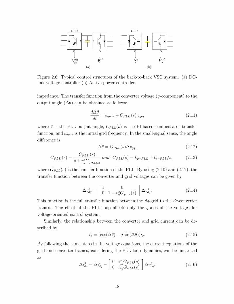
Figure 2.6: Typical control structures of the back-to-back VSC system. (a) DC-link voltage controller (b) Active power controller.
impedance. The transfer function from the converter voltage (q-component) to the
output angle (∆θ) can be obtained as follows:
d∆θ
dt= ωgrid + CPLL (s) vgq, (2.11)
where θ is the PLL output angle, CPLL(s) is the PI-based compensator transfer
function, and ωgrid is the initial grid frequency. In the small-signal sense, the angle
difference is
∆θ = GPLL(s)∆vgq, (2.12)
GPLL (s) =CPLL (s)
s+ vogCPLL(s)
and CPLL(s) = kp−PLL + ki−PLL/s, (2.13)
where GPLL(s) is the transfer function of the PLL. By using (2.10) and (2.12), the
transfer function between the converter and grid voltages can be given by
∆vcdq =
[1 00 1− vogGPLL
(s)
]∆vgdq. (2.14)
This function is the full transfer function between the dq-grid to the dq-converter
frames. The effect of the PLL loop affects only the q-axis of the voltages for
voltage-oriented control system.
Similarly, the relationship between the converter and grid current can be de-
scribed by
ic = (cos(∆θ)− j sin(∆θ))ig. (2.15)
By following the same steps in the voltage equations, the current equations of the
grid and converter frames, considering the PLL loop dynamics, can be linearized
as
∆igdq = ∆icdq +
[0 ioqgGPLL(s)0 iodgGPLL(s)
]∆vgdq. (2.16)
18
VdcPgPsPdc2Pdc1
GridPower source
Figure 2.7: Energy balance on the dc-link.
2.4 Output Impedance with Outer Loops (Ac-
tive Component)
Generally and under vector current control there are two schemes exist for gener-
ating the d -axis component of the reference current. Figure 2.6(a) shows the first
control structure of Back-to-back VSC system, where the GSC control is utilized
to control the dc-link voltage. In this scheme, the remote (machine-side) converter
is used to control the active power (e.g.,variable speed operation in the maximum
power point tracking (MPPT) mode for wind system). The second scheme is shown
in Figure 2.6(b), where the GSC is employed to control the power injection into
the grid, whereas the remote (machine-side) converter is configured to regulate the
dc-link voltage.
2.4.1 DC-Link Voltage Control
The outer dc-link voltage control loop is utilized to generate the reference active
component to the current controller to regulate the dc-link voltage. This reference
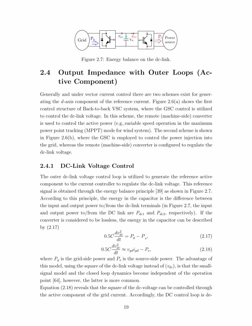
signal is obtained through the energy balance principle [39] as shown in Figure 2.7.
According to this principle, the energy in the capacitor is the difference between
the input and output power to/from the dc-link terminals (in Figure 2.7, the input
and output power to/from the DC link are Pdc1 and Pdc2, respectively). If the
converter is considered to be lossless, the energy in the capacitor can be described
by (2.17)
0.5Cdv2
dc
dt= Pg − P s, (2.17)
0.5Cdv2
dc
dt≈ vgdigd − Ps, (2.18)
where Pg is the grid-side power and Ps is the source-side power. The advantage of
this model, using the square of the dc-link voltage instead of (vdc), is that the small-
signal model and the closed loop dynamics become independent of the operation
point [64], however, the latter is more common.
Equation (2.18) reveals that the square of the dc-voltage can be controlled through
the active component of the grid current. Accordingly, the DC control loop is de-
19

2ref
dcV( )dcC s-
+
2
dcV
ref
di
sPPH
-)(ˆ
1
gvg VHV
gV vH
ref
di-
ref
gP
gP
+ )(sCP
LPF
(a) (b)
LPF
Figure 2.8: Control structures of GSC. (a) DC-bus voltage control. (b) Directactive power control.
signed as shown in Figure 2.8(a), which shows the details of the corresponding
control loops. The dc-link voltage control loop is designed with source-side power
(Ps) feed-forward control, which minimizes the impact of the source dynamics on
the grid-side converter dynamics and improves the dc-link voltage control perfor-
mance. Both the grid voltage and source power might be processed by a low-pass
filter (Hp and Hv ) in Figure 2.8(a) for filtering purposing; however, they have
minimal impact on the impedance profile. Figure 2.8(b) shows the active power
control, which is designed with a simple direct PI–controller (Cp(s)). The equa-
tions of the active and reactive powers of the grid in the dq-frame are represented
as follows:
Pg = vgdigd + vgqigq, (2.19a)
Qg = vgqigd − vgdigq. (2.19b)
In the vector control strategy, the d -voltage component is aligned with the grid
voltage (which yields vgq=0). Therefore, (2.19) can be simplified by
Pg = vgdigd (2.20a)
Qg = −vgdigq. (2.20b)
It is understood from (2.20) that the active power can be controlled by regulating
the direct-current component, and that the reactive power can be controlled by
regulating the quadrature current component. Then, the small-signal models for
the active and reactive power equations in (2.19) with the observation from (2.20)
are
∆P g = ∆vgdiogd + ∆igdv
og + ∆vgqi
ogq, (2.21a)
∆Qg = ∆vgqiogd −∆vgdi
ogq −∆igqv
og . (2.21b)
20
By using (2.8)-(2.21) , the small-signal model, which relates the change in the direct
reference current due to the change in the grid voltage components by considering
the dc-outer loop ( i.e., the contribution of the dc-outer loop in the impedance
prolife), can be obtained as
∆irefd = T1∆vgd + T2∆vgq, (2.22)
where
T1 = −
[po − pofcc(s)Hp(s) +
(vog)2Zcc−1(s)
]Cdc (s)(
vog)2
(sC + Cdcfcc(s))+poHp(s)(vog)2
,
T2 = −Cdc (s)
{Qo(
vog)2
(sC + Cdcfcc (s))
}.
As shown in above, T1 depends on the ctive power injection, whereas T2 depends
on the reactive power injection of the VSC system.
2.4.2 Active Power Control
Another controller in the grid-side converter is the direct power controller shown
in Figure 2.8(b), where the d-axis component of the reference current is generated
by processing the error between the reference power, which is normally obtained
from a lookup table that relates the generator speed to the active output power
for a wind power system, and the grid power [65],[59]. Accordingly, the d -axis
reference current generation dynamics is governed by
irefd = Cp (s)(prefg − pg
), Cp (s) = kp−p + ki−p/s. (2.23)
With prefg = pog, the small-signal version of (2.23) is
∆irefd = −Cp (s) ∆pg. (2.24)
By using (2.7), (2.8) and (2.21), the small-signal model of the reference d -axis
current generation dynamics will be altered under the grid power control mode.
The modified model can be given by
∆irefd = T ′1∆vgd + T ′2∆vgq (2.25)
T ′1 = −Cp(s)
{P o/vog + Zcc
−1(s)vog + P oGPLL(s)
1 + Cp(s)vogfcc(s)
}, T ′2 = Cp(s)
{Qo/vog
1 + Cp(s)vogfcc(s)
}.
21

-
ref
gv
gv
+ ( )VC s
ref
qi-
ref
gQ
gQ
+ )(sCQ 0
ref
qiref
qi
(a) (b) (c)
Figure 2.9: Control mode of grid-side converter of VSCs. (a) V -mode, (b) Q-modeand (c) Unity power factor mode.
2.5 Output Impedance with Outer Loops (Quadra-
ture Component)
Different control modes can be used to control the grid-side converter of the VSCs.
As the grid code are being updated and requires large wind-generation units to
support the system voltage (especially in weak grids) and provide reactive power
support [66]. The effect of these operational modes on the output impedance of the
VSC must be addressed. Besides controlling the dc-link voltage (or active power),
the VSC can be utilized to regulate the ac-voltage (V -mode) at the PCC, control
the injected reactive power (Q-mode), or control the VSC at a unity power factor
(UPF-mode). Figure 2.9 depicts the controller blocks of these control modes.
2.5.1 AC Voltage Control Mode
In this mode, the ac-voltage at PCC is regulated, and the quadrature component of
the reference current is obtained by processing the difference between the measured
grid voltage (at the PCC) and the reference voltage is expressed as
irefq = Cv(s)(vrefg − vg
), Cv(s) = kp−v + ki−v/s. (2.26)
with vrefg = vog , the small-signal version of (2.26) is
∆irefq = −Cv(s)∆vgd. (2.27)
To be consistent in comparing the effect of the control mode, a general form, which
describes the current generation dynamics in the quadrature channel, is given by
∆irefq = F1∆vgd + F2∆vgq (2.28)
F1 = −Cv(s) and F2 = 0.
22

2.5.2 Reactive Power Control Mode
The error between the measured reactive power at the PCC and the desired val-
ues is processed by a PI controller to provide the reference signal for the current
controller. This process can be modeled by
irefq = CQ(s)(Qrefg −Qg
), CQ(s) = kp−Q + ki−Q/s. (2.29)
with Qrefg = Qo
g, the small-signal version of (2.25a) is
∆irefq = −CQ(s)∆Q. (2.30)
Substituting (2.21b) in (2.30) yields
∆irefq = −CQ (s){
∆vgqiogd −∆vgdi
ogq −∆igqv
og
}. (2.31)
After simplifying (2.31), the current generation dynamics in the quadrature
channel with reactive power control can be given by
∆irefq = F ′1∆vgd + F ′2∆vgq (2.32)
where
F′
1 = CQ (s)
{Qo/vog
1− vogCQ (s) f cc (s)
},
F′
2 = CQ (s)
{ po
vog+ Zcc
−1 (s) vog −po
vogGPLL (s)
1− vogCQ (s) f cc (s)
}.
As shown in (2.32), F ′1 depends on the reactive power injection, whereas F ′2
depends on the active power injection of the VSC system.
2.5.3 Unity Power Factor Controller
Operating a VSC at the unity power factor is very common, especially in normal
operation conditions. In this mode, the q-component of the reference current is
set to zero, which can be a special case of (2.32) with F ′1 = F ′2 = 0.
Table2.1 summarizes the impedance elements contribution from the outer loop
reactive components.
23

Table 2.1: Impedance elements of the outer loop quadrature channel.V-mode Q-mode UPF-mode
F 1 −Cv(s) CQ(s){
Qo/vog1−vogCQ(s)f
cc(s)
}0
F 2 0 CQ(s)
{po
vog+Zcc
−1(s)vog−po
vogGPLL(s)
1−vogCQ(s)fcc
(s)
}0
2.6 Overall Impedance Model
Combining all the obtained equations, the resulting expression admittance (impedance)
is shown below. This output impedance expression will be used in the next chapter
to study the impact of each loop on the impedance profile and to indentify the
key contributors in the impedance profile. Figure 2.10 depicts how the control
elements and loops are interconnected to form the output impedance of the VSCs,
and indicates the contribution from each control loop element. Figure 2.11 provides
another representation of how the change/ perturbation in the grid current and
voltage penetrate through the control system, yielding the impedance response.
Z11V SC = vog ∗ Zcc−1 +GPLLpo + vogF2fcc − vog
2GPLLZcc−1)/(A+B)
Z12V SC = −(GPLLQo + vogT 2
fcc)/(A+B)
Z21V SC = −(vogF 1fcc)/(A+B)
Z22V SC = ((vogy + vo
gT
1fcc)/(A+B)
A = Zcc−1{vog − vog
2GPLLZcc−1 +GPLLp
o}
B = GPLLfcc {T1Po − F1Q
o}+ Zcc−1fcc
{vogF 2
+ vogT 1
}+
fcc2{vogF2T1 − vogF1T2
}+GPLLfccZcc
−1T1vog
2.
2.7 Controller Design Criteria
This section provides the general design guidelines of the VSC control parameters
under practical design constraints. The designed parameters are used to assess the
base-line output impedance dynamics and their interactions with the power grid.
The control parameters are designed by using frequency “loop-shaping” techniques
and shown in the following subsections [39].
24
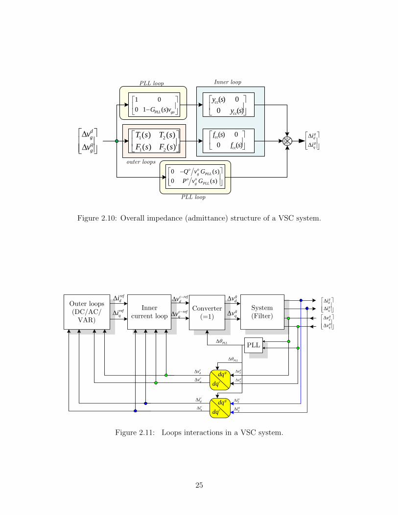
)(0
0)(
sf
sf
cc
cc
)(0
0)(
sy
sy
cc
cc1 0
0 1 ( )PLL goG s v
0 ( )
0 ( )
o o
g PLL
o o
g PLL
Q v G s
P v G s
q
g
d
g
v
v
+++1 2
1 2
( ) ( )
( ) ( )
T s T s
F s F s
Inner loop
outer loops
PLL loop
PLL loop
g
d
g
q
i
i
Figure 2.10: Overall impedance (admittance) structure of a VSC system.
System (Filter)
Converter(=1)
g
d
g
q
i
i
g
d
g
q
v
v
Inner current loop
Outer loops(DC/AC/
VAR)
g
dv
g
qv
ref
di
ref
qi
c ref
dv
c ref
qv
PLL
PLL
g
dv
g
qv
g
di
g
qi
c
dv
c
qv
c
di
c
qi
gdqcdq
gdqcdq
PLL
Figure 2.11: Loops interactions in a VSC system.
25

A 100 MVA (aggregated) VSC-based wind-turbine is connected to the stud-
ied system. The IEEE FBM is adopted to demonstrate the impact of the output
impedance of a VSC on sub-synchronous damping. The parameters of the IEEE
FBM are given in [18] and presented in Appendix B. The switching frequency is
chosen to be 2 kHz (i.e., 33.33 p.u. at 60 Hz base-frequency), which is a typ-
ical switching frequency for modern high-power VSCs. The grid-side R-L filter
(including the connection transformer) parameters are 0.15 p.u. inductance and
0.015 p.u. resistance. The value of the filter inductor is chosen to minimize the
ripple in the injected current and to cope with the short-circuit requirements of
the VSC.
A. Inner Current Control Loop
By choosing the gains for the PI current controller as kp−cc = ωccL ,ki−cc = ωccR,
where ωcc is the bandwidth of the controller, the closed-loop transfer function of
the current controller that is described by (2.7) can be simplified as
f cc(s) =ωcc
s+ ωcc. (2.33)
where f cc(s) is the closed-loop current control dynamics.
The current control loop design criterion is dictated mainly by the filter pa-
rameters and the switching frequency of the converter. The switching frequency
is chosen as 2 kHz. The recommended bandwidth for the current controller is
selected as one-fifth of the switching frequency[67], which yields a bandwidth of
6.67 p.u. based on a 60 Hz power frequency. Accordingly, the current controller
gains can be calculated as kp−cc = 1.0 p.u. and ki−cc = 0.1 p.u. (which is enough
to eliminate the steady state error).
B. Outer Loops (DC/Power, Voltage/Reactive Loops)
To facilitate reliable and stable cascaded control operation, the recommended
bandwidth for the outer controller is at least five times lower than that of the
inner loop [62]. The bandwidth of the dc-voltage control loop is chosen to be
slower than that of the inner loop, with a bandwidth 10% of that of the inner loop
(i.e., BWDC = BW cc/10 ). The dynamics of the current-control loop (fcc(s)) is
much faster than the dynamics of outer loops; therefore, it is reasonable to assume
that fcc(s) = 1 within the bandwidth of the outer loops. The closed loops transfer
function of the dc-link voltage control loop is shown in Figure 2.12(a) and can be
given by
26
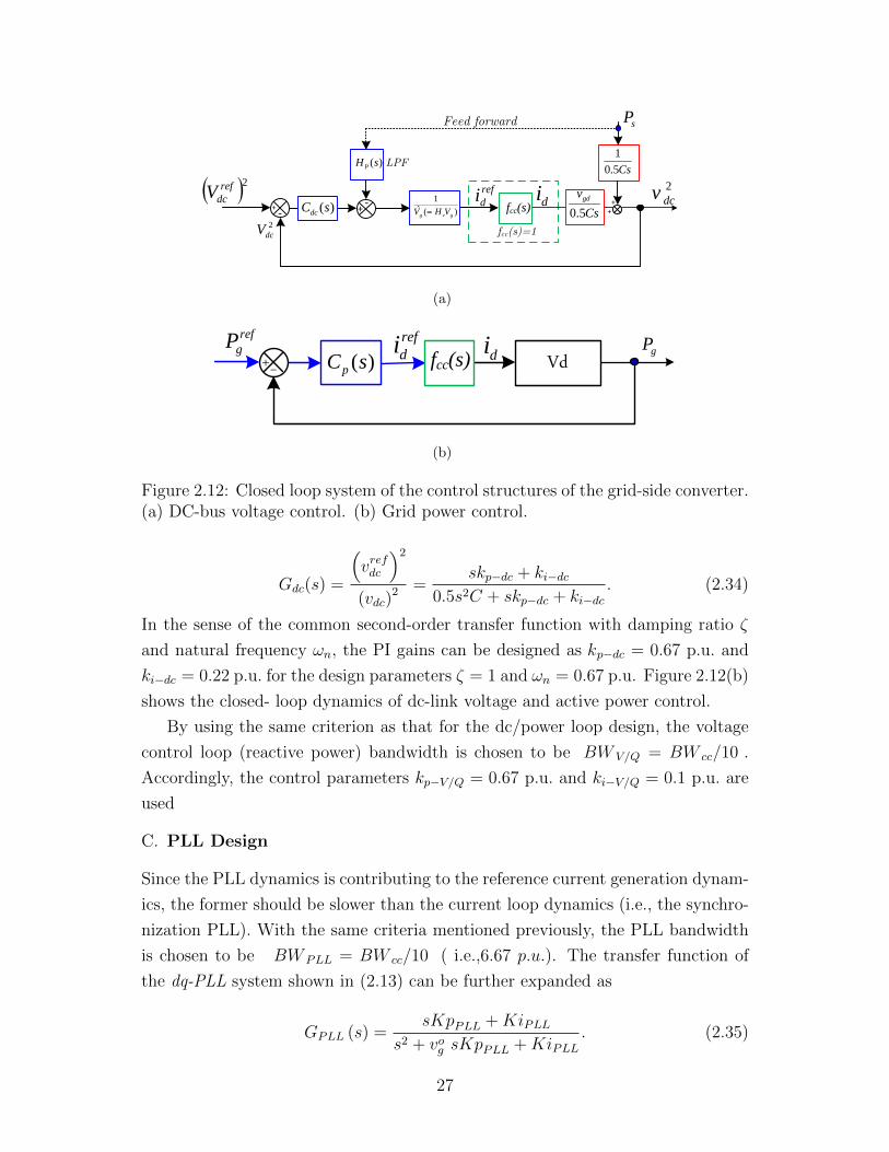
difcc(s) 2ref
dcV( )dcC s-
+
2
dcV
ref
di
( )PH s
-)(ˆ
1
gvg VHV
LPF
Feed forward
2
dcv
sP
+++ 0.5
gdv
Cs
1
0.5Cs
fcc(s)=1
(a)
-
gP+ ( )pC s difcc(s)
ref
diref
gPVd
(b)
Figure 2.12: Closed loop system of the control structures of the grid-side converter.(a) DC-bus voltage control. (b) Grid power control.
Gdc(s) =
(vrefdc
)2
(vdc)2 =
skp−dc + ki−dc0.5s2C + skp−dc + ki−dc
. (2.34)
In the sense of the common second-order transfer function with damping ratio ζ
and natural frequency ωn, the PI gains can be designed as kp−dc = 0.67 p.u. and
ki−dc = 0.22 p.u. for the design parameters ζ = 1 and ωn = 0.67 p.u. Figure 2.12(b)
shows the closed- loop dynamics of dc-link voltage and active power control.
By using the same criterion as that for the dc/power loop design, the voltage
control loop (reactive power) bandwidth is chosen to be BW V/Q = BW cc/10 .
Accordingly, the control parameters kp−V/Q = 0.67 p.u. and ki−V/Q = 0.1 p.u. are
used
C. PLL Design
Since the PLL dynamics is contributing to the reference current generation dynam-
ics, the former should be slower than the current loop dynamics (i.e., the synchro-
nization PLL). With the same criteria mentioned previously, the PLL bandwidth
is chosen to be BW PLL = BW cc/10 ( i.e.,6.67 p.u.). The transfer function of
the dq-PLL system shown in (2.13) can be further expanded as
GPLL (s) =sKpPLL +KiPLL
s2 + vog sKpPLL +KiPLL. (2.35)
27

The transfer function in (2.35) is similar to the standard second-order transfer
function with a natural frequency ωn and damping ratio (ζ). Therefore, the PI
controller gains can be obtained as KiPLL = ω2n and Kp−PLL = 2ζωn. Accordingly,
the control parameters are designed as kp−PLL = 1.34 p.u and ki−PLL = 0.45 p.u.
28

Chapter 3
Impedance Analysis and DynamicInteraction Assessments 2
In this chapter, the output impedance derived in Chapter2 is analyzed and charac-
terized. Furthermore, the output impedance is used to analyze the electrical damp-
ing when a VSC system is installed nearby a multi-mass synchronous generator.
Several aspects are considered: the impact of the inner and outer loops, the effect
of the control structures and modes, the influence of the operating points on the
output impedance, and the electrical damping. The impact of switching frequency
and controller bandwidths is also pointed out.
3.1 Electrical Damping Analysis Methods
The electrical damping approach, as explained in Chapter 1, is adopted to quantify
the impact of VSCs on the sub-synchronous electrical damping characteristics. The
electrical transfer function is described as the ratio between the changes in electrical
torque and the change in rotor speed (or rotor angle). This criterion is based on
evaluating the resistive part of the transfer function of the electrical damping (i.e.,
real-part of Ge(s)) as described by
De(s) = Real {Ge(s)} = Real
{4Te4ω(4δ)
}, (3.1)
where Ge is the electrical transfer function; De is the electrical damping; 4Te is the
change in electrical torque, and 4ω(4δ) is the change in the rotor speed (or the
rotor angle). The electrical transfer function can be extracted from small-signal
models of the synchronous generator and the network components. Figure 3.1
2 This work is publised in IEEE Systems Journal [68].
29

)(sTeD(s)B(s) C(s)
si sv
A(s)
s)(s r
E(s)
Figure 3.1: Electrical damping state-space model..
TZ
Synch. gen Tr. Grid
SZ
Multi-mass mech. sys
Exe Gen HPLPA LPB IP
Full scale VSC systemPCC
Filter Power Source
RL XL
Figure 3.2: System under the study (IEEE FBM with a full-scale VSC system).
shows the small-signal block diagram of the overall system (the synchronous gen-
erator and network components).
Thus, the electrical damping transfer-function model of the overall system is
given by (for calculating the real-part of the function, s is replaced by (jω) )
Ge (s) = 4Te(s)4δ(s) = s(A(s) +D(s)E(s)(I − C(s)E(s))−1B(s))
De(jω) = Re{Ge (jω)},
}(3.2)
where A(s), B(s), C (s), and D(s) are the synchronous generator state-space ma-
trices; and E (s) is the representation of the network, which is the equivalent
impedance seen by the machine terminals. Derivations of these matrices are given
in Appendix A. Figure 3.2 shows the circuit diagram of the studied system. The
IEEE first benchmark (FBM) for sub-synchronous studies is adopted for theoreti-
cal analysis and simulation results. A full-scale VSC is added to interface a power
source (e.g., a full-scale wind farm) to the ac network. In this study, the uncompen-
sated system is considered as a common power system configuration. The impact
of VSCs in a serially-compensated system is discussed in Chapter 5. The main
focus of this Chapter is on sub-synchronous interactions due to the VSC impact
on the system damping. Figure 3.3 shows the representation of the VSC, which
is represented as a Norton equivalent circuit (i.e., current source in parallel with
30

TZ
Synch. gen
Tr.
Grid
Transmision line LXLR
sXsR
()
VSC
Ys
Representation of VSC system
Zeq
ZL=RL+jXL Zs=Rs+jXs
Figure 3.3: System representation with VSC equivalent model.
incremental admittance). The derived output impedance in Chapter 2 is used to
study the overall system damping characteristics and interactions.
The matrix transfer function E (s) in Figure 3.1. is simply the equivalent
impedance reflected to the machine terminals. Therefore, the incremental impedance
of the VSC directly affects E (s) and dictates the interactions between the VSC sys-
tem and the power system. From Figure 3.3, the equivalent impedance is expressed
by
E (s) = Zeq (s) = ZT (s) +ZV SC (s)Zs(s)
ZV SC(s)+Zg(s), (3.3)
where Zg (s) = ZL (s) + Zsys (s) .
3.2 System Modeling (Network and Synchronous
Machine Models)
The synchronous generator used in this study is a typical salient pole synchronous
generator which is normally modeled in the dq rotor-reference frame. In this
model, the field-winding and three damper windings are considered. The general
state-space model of a synchronous machine can be described as shown in [61]
i̇=−L−1 (R+ωN) i−L−1v, (3.4)
where L is the inductance matrix, R is the resistance matrix, N is the speed
voltage matrix, and i and v are the current and voltage matrices.. Appendix A
illustrates the contents of these matrices. The entire power system needs to be
linearized around an operation point. The derivation and linearization process of
this equation is given in Appendix A. Since the analysis is performed in the dq-
synchronous reference-frame, the network-side dynamics need also to be transferred
to the synchronous reference-frame. The resulting impedance matrix of the studied
31

system (Figure 3.3) in the dq-frame can be described as follows:
Zg (s) =
[Zs11(s) Zs12(s)Zs21(s) Zs22(s)
]=
[Rg + sXg −Xg
Xg Rg + sXg
](3.5)
Rg = RL +Rs, Xg = XL +Xs
ZT (s) =
[ZT11(s) ZT12(s)ZT21(s) ZT22(s)
]=
[RT + sXT −Xt
XT RT + sXT
], (3.6)
where XL , Xs , and XT are the line, system, and transformer, reactance respec-
tively; and RL , Rs , and RT are the line, system, and transformer resistance,
respectively .
3.3 IEEE FBM Torsional Analysis
Table 3.1 presents the torsional frequencies for the mechanical system of the studied
system (IEEE FBM). This table shows five modes in the sub-synchronous range
(based on 60 Hz). The main purpose of this chapter is to investigate the impact
of control elements and functions of a full-scale VSC on the electrical damping
around each mode.
Table 3.1: Torsional Modes of IEEE FBMMode 1 2 3 4 5
Frequency [Hz] 15.71 20.21 25.55 32.25 47.46[p.u.] (0.261) (0.337) (0.426) (0.5737) (0.791)
3.4 Analysis of Output Impedance of VSC
This section analyzes the properties and characteristics of the output impedance
and the effect of different control loops on output impedance shaping. In this con-
text, “control mode” indicates the V-mode, Q-mode, or UPF-mode and “control
structure” indicates the dc-link voltage control or active power control.
3.4.1 Analysis of the Internal Impedance
In this thesis, the term “internal impedance” indicates the resulting impedance
when only the inner current controller loop is considered (i.e., Zcc(s)). The output
impedance of a VSC can be simply expressed as
ZV SC = RV SC ± jXV SC . (3.7)
32

0
1
2
3
Mag
nit
ude
(p.u
.)0.2 0.4 0.6 0.8 1 1.2 1.4 1.6 1.8
-180
-135
-90
-45
0
Phas
e (d
eg)
Frequency ([p.u.])
negative resistance region
Figure 3.4: Internal impedance profile.
The positive resistance appears in the Bode plot if the phase angle of the impedance
lies on the first and fourth quarters:
{−90 < θZV SC< 90} → RV SC > 0. (3.8)
By considering only the inner current control loop, the impedance matrix becomes
diagonal [see (2.8)]; this result yields Z11 (s) = Z22 (s) = Zcc (s) and Z12 (s) =
Z21 (s) = 0. Using the control parameters designed in Chapter 2, Figure 3.4
shows the frequency response of the output impedance as a function of the sub-
synchronous frequency. It is worth to mention that the impedance, in this case, is
independent of the injected power level. The appearance of the positive impedance
occurs for (f>0.2 p.u.). For further investigations, an expression of the real-part
can be developed as
Re {Zcc(s)} = kp +R + ωffL−ωffkiω2
. (3.9)
From (3.9) it is understood that a frequency range exists where the negative
resistance (resistance) appears. Then the frequency boundary where the positive
resistance appears is given by
ω >
√ωffki
kp +R + Lωff. (3.10)
Three active components are affecting the internal impedance: the proportional
gain, the integral gain, and the feed-forward bandwidth. Increasing both the in-
tegral gain and feed-forward bandwidth increases the negative resistance, while
increasing the proportional gain increases the positive impedance.
33
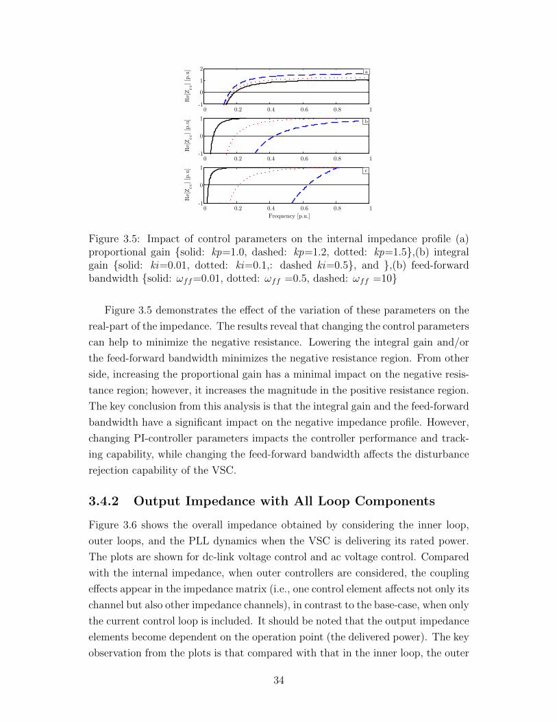
0 0.2 0.4 0.6 0.8 1-1
0
1
2
Re[
Zcc
] [p
.u]
0 0.2 0.4 0.6 0.8 1-1
0
1
Re[
Zcc
] [p
.u]
0 0.2 0.4 0.6 0.8 1-1
0
1
Re[
Zcc
] [p
.u]
Frequency [p.u.]
a
b
c
Figure 3.5: Impact of control parameters on the internal impedance profile (a)proportional gain {solid: kp=1.0, dashed: kp=1.2, dotted: kp=1.5},(b) integralgain {solid: ki=0.01, dotted: ki=0.1,: dashed ki=0.5}, and },(b) feed-forwardbandwidth {solid: ωff=0.01, dotted: ωff =0.5, dashed: ωff =10}
Figure 3.5 demonstrates the effect of the variation of these parameters on the
real-part of the impedance. The results reveal that changing the control parameters
can help to minimize the negative resistance. Lowering the integral gain and/or
the feed-forward bandwidth minimizes the negative resistance region. From other
side, increasing the proportional gain has a minimal impact on the negative resis-
tance region; however, it increases the magnitude in the positive resistance region.
The key conclusion from this analysis is that the integral gain and the feed-forward
bandwidth have a significant impact on the negative impedance profile. However,
changing PI-controller parameters impacts the controller performance and track-
ing capability, while changing the feed-forward bandwidth affects the disturbance
rejection capability of the VSC.
3.4.2 Output Impedance with All Loop Components
Figure 3.6 shows the overall impedance obtained by considering the inner loop,
outer loops, and the PLL dynamics when the VSC is delivering its rated power.
The plots are shown for dc-link voltage control and ac voltage control. Compared
with the internal impedance, when outer controllers are considered, the coupling
effects appear in the impedance matrix (i.e., one control element affects not only its
channel but also other impedance channels), in contrast to the base-case, when only
the current control loop is included. It should be noted that the output impedance
elements become dependent on the operation point (the delivered power). The key
observation from the plots is that compared with that in the inner loop, the outer
34

0
2
4
6
8
10
Mag
nit
ude
(p.u
.)0.2 0.4 0.6 0.8 1 1.2 1.4 1.6 1.8 2
-360
-270
-180
-90
0
Phas
e (d
eg)
Frequency ([p.u.])
negative resistance region
Figure 3.6: Output impedance of VSC; circled: Z cc, solid: Z 11, dotted: Z 21,dashed: Z 22.
loops negatively contribute to the impedance profile where the negative resistance
region is extended. The appearance of positive impedance in Z11 occurs at f =0.70
p.u., and Z 22 has negative resistance in the overall sub-synchronous frequency
range, while Z 21 has a positive impedance only in the low-frequency range (f<0.5.
p.u.).
3.4.3 Impact of Phase-Locked Loop (PLL) Dynamics
By investigating the impedance matrix, the dynamic activity of the PLL is found
to be dependent on the control mode and the operating condition. The plots in
this subsection are obtained, for simplicity, under dc-link voltage control and the
unity power factor mode, so the PLL control loop affects only the Z 22element in the
Z -matrix elements. Figure 3.7 demonstrates the effect of the PLL controller on the
output impedances under three operating conditions: when the VSC is fully loaded,
unloaded, and when no PLL is used. As it can be seen, when the VSC is fully
loaded, the negative resistance appears in the entire sub-synchronous frequency
range. Under the no-load condition, a positive impedance is only achieved at the
very low frequency range ( f<0.1 p.u.). Generally speaking, the impact of the
operational point becomes insignificant at the high-frequency range (f>0.6p.u.).
However, a higher magnitude is obtained under the no-load condition. In the case
of no PLL used, the (Z 22) term converges to the internal impedance (Zcc). The
PLL controller tracks the voltage angle and tries to lock the converter to this angle.
When a system disturbance occurs which is reflected by the voltage variation, the
phase-angle increases and hence reduces the positive impedance of the converter.
35

0
1
2
3
Mag
nit
ude
(p.u
.)0.2 0.4 0.6 0.8 1 1.2 1.4 1.6 1.8 2
-360
-270
-180
-90
0
Phas
e (d
eg)
Frequency ([p.u.])
negative resistance region
Figure 3.7: Effect of the PLL on Z 22 : (circled: Zcc), (solid line: P=1.0 p.u),(dotted line: P= 0). (dashed line: No PLL:).
0
0.5
1
1.5
2
Mag
nit
ude
(p.u
.)
0.2 0.4 0.6 0.8 1 1.2 1.4 1.6 1.8-360
-270
-180
-90
0
Phas
e (d
eg)
Frequency ([p.u.])
negative resistance region
Figure 3.8: Effect of AC voltage controller on output impedance Z 21. (solid line:with ac-voltage control loop), (dashed line: without ac-voltage control loop).
3.4.4 Impact of AC-Voltage Control Loop
The AC-voltage controller affects the Z 21 element in the impedance matrix. Fig-
ure 3.8 shows the Z 21 profile with and without ac-voltage control. When there is
no ac-voltage control, the reactive current reference is set at zero, which is a typical
unity power factor mode (i.e., Z 21=0). Clearly, with the ac-voltage control loop
Z 21 has a negative resistance in the entire sub-synchronous frequency ranges, ex-
cept in the middle-frequency ranges (0.4 < f < 0.6p.u.) where a positive resistance
appears.
36
3.5 Sensitivity Studies and Electrical Damping
Analyses
In this section, the effect of different control modes and structures of the interfacing
VSC system on impedance profile and the overall electrical damping of the studied
system is presented.
3.5.1 Electrical damping Profiles
Figure 3.9 shows the electrical damping of the overall system along with the real-
part of impedance elements of VSC for three cases: without the VSC (base-case),
with the VSC with only inner loops, and with the VSC with all the control loops.
This figure reveals that for the VSC with only inner current control loop, the
electrical damping profile starts improving (for frequency greater than 0.2 p.u.),
because of the appearance of the positive impedance of the VSC. This improvement
starts almost with the same frequency as the real-part of the internal impedance
(Zcc) becomes positive. As the positive resistance of the VSC appears, higher
positive damping is added to the system. The same results are obtained when
the synchronous generator is either not loaded or fully loaded. When the outer
loops are considered, the overall electrical damping is degraded due to the negative
resistance behavior induced by the outer loops (negative resistance appears in most
of impedance elements), which is mainly associated with the PLL dynamics and
the tight-regulation behavior of the VSC.
3.5.2 Effect of the Loading Condition of VSC
Figure 3.10 shows the effect of the loading condition of the VSC on the output
impedance and electrical damping. When the VSC is fully loaded, the real-part
of Z22 becomes completely negative in the entire sub-synchronous range. This
result can be attributed to the impact of the PLL, whereas an improvement in the
positive real-part of Z11 in the low-frequency range is obtained. Similar obser-
vations hold for the real-part of Z21. However, the impact of the initial loading
appears only at the lower-frequency range (f<0.6 p.u.). Generally speaking, worst
case occurs when VSC is fully loaded.
3.5.3 Effect of Reactive Power Injection
Figure 3.11 shows the effect of the reactive power injection by the VSC on the out-
put impedance and electrical damping for an unloaded and fully loaded VSC, re-
37

0 0.2 0.4 0.6 0.8 1−3
−2
−1
0
1
2
3
De
(p.u
.)Frequency [p.u.]
(a)
0 0.2 0.4 0.6 0.8 1−1
0
1
2
Re[
Zcc
] (p.
u.)
0 0.2 0.4 0.6 0.8 1
−5
0
5
Re[
Z11
] (p.
u.)
0 0.2 0.4 0.6 0.8 1
−5
0
5
Re[
Z21
] (p.
u.)
0 0.2 0.4 0.6 0.8 1
−5
0
5
Re[
Z22
] (p.
u.)
Frequency [p.u.]
(b)
Figure 3.9: (a) Electrical damping (solid: base-case, dashed: current controller,dotted: with outer loops). (b) Real part of output impedance elements.
0 0.2 0.4 0.6 0.8 1−5
0
5
De
(p.u
.)
0 0.2 0.4 0.6 0.8 1−5
0
5
Re[
Z11
] (p.
u.)
0 0.2 0.4 0.6 0.8 1−5
0
5
Re[
Z21
] (p.
u.)
0 0.2 0.4 0.6 0.8 1−5
0
5
Re[
Z22
] (p.
u.)
Frequency [p.u.]
Figure 3.10: Effect of the loading condition : Electrical damping and Real-part ofZ11, Z21 and Z22 (solid line : P= 0), (dashed line : P=1.0 p.u. ).
38

spectively. Figure 3.11 reveals that the reactive power injection has a significant im-
pact on the impedance elements. For the unloaded case (P=0 p.u.), when the VSC
works in the STATCOM mode, the reactive power injection affects the impedance
elements; Z 22 becomes completely negative in the entire sub-synchronous range,
whereas an improvement in the real-part of Z11 in the low-frequency range is at-
tained with no significant effect on the high-frequency range. Similar observations
hold for Z21. When the VSC is fully loaded (P=1.0 p.u.) [see Figure 3.11(b)], the
effect of the reactive power injection appears only in the off-diagonal impedance
elements. Generally, the effect of the reactive power disappears at high frequen-
cies (>0.5 p.u.). In conclusion, there is a positive impact on (Z 11 and Z 21) and
a negative impact on (Z 22 and Z 12 ) which cancel each other out and have an
insignificant impact on the damping profile; however, there is little improvement,
under zero reactive power injection, in the overall electrical damping, as it is shown
in the lower traces of Figure 3.11.
3.5.4 Effect of Operational Control Mode
Figure 3.12 shows the effect of the operational control mode (the V -mode, Q-mode
and unity PF mode) on the electrical damping and the output impedance char-
acteristics. The results shown in this figure are obtained when all the generating
units deliver their rated power to the system. Only two components of the output
impedance matrix are affected: Z 21 and Z 22. As Figure 3.12 reveals, when the
VSC operates in the Q-mode, the output impedance becomes more negative at
low frequencies (f<0.5 p.u.) and highly positive at high frequencies (f >0.5 p.u.).
Hence, the electrical damping is improved. The opposite occurs when the VSC is
used to control the voltage at the PCC, because only the d -axis component of the
grid voltage vgd is involved in the output impedance in the V -mode, whereas both
the d - and q-axis components of the grid voltage are involved when the Q-mode
is activated. In other words, the injected perturbed current is more dependent
on the grid voltage when the injected current is used to regulate the grid voltage.
For unity power factor control, the impedance matrix becomes off-diagonal, so the
effect from the other impedance elements is reduced, and the impedance becomes
less sensitive to the frequency and to the number of the loops involved.
3.5.5 Effect of Control Structure
The effect of the control structure is analyzed in this subsection. The analysis
of the output impedance matrix (in Chapter 2)shows that the control structure
39

0 0.2 0.4 0.6 0.8 1−10
−505
Re[
Z11
] (p.
u)
0 0.2 0.4 0.6 0.8 1−5
0
5
Re[
Z12
] (p.
u)
0 0.2 0.4 0.6 0.8 1−5
0
5
Re[
Z21
] (p.
u)
0 0.2 0.4 0.6 0.8 1−15−10
−505
Re[
Z22
] (p.
u)
0 0.2 0.4 0.6 0.8 1−1
012
De
(p.u
)
Frequency [p.u.]
(a)
0 0.2 0.4 0.6 0.8 1−10
−505
Re[
Z11
] (p.
u)
0 0.2 0.4 0.6 0.8 1−5
0
5
Re[
Z12
] (p.
u)
0 0.2 0.4 0.6 0.8 1−5
0
5
Re[
Z21
] (p.
u)
0 0.2 0.4 0.6 0.8 1−15−10
−505
Re[
Z22
] (p.
u)
0 0.2 0.4 0.6 0.8 1−1
012
De
(p.u
)
Frequency [p.u.]
(b)
Figure 3.11: Effect of the injected reactive power on the output impedance andelectrical damping (solid: zero reactive power, dashed: 0.2 p.u. reactive power)(a) with P= 0 and (b) with P=1.0 p.u.
0 0.2 0.4 0.6 0.8 1−5
0
5
De
(p.u
)
0 0.2 0.4 0.6 0.8 1−5
0
5
Re[
Z21
] (p.
u)
0 0.2 0.4 0.6 0.8 1−2
0
2
Re[
Z22
] (p.
u)
Frequency [p.u.]
Figure 3.12: Effect of the control mode on the output impedance and electricaldamping (solid: V mode, dotted: Q mode, dashed: Unity PF mode) (Z 22 is samein case of unity PF and PV mode).
40
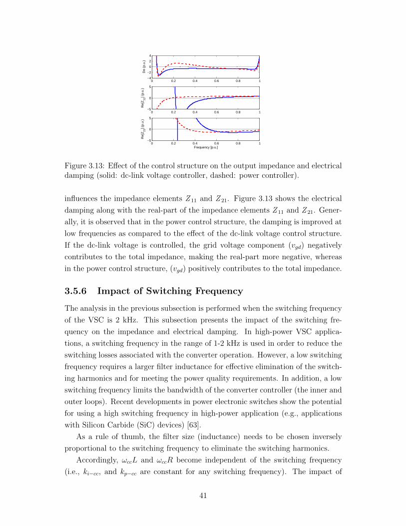
0 0.2 0.4 0.6 0.8 1−4
−2
0
2
4
De
(p.u
.)
0 0.2 0.4 0.6 0.8 1−5
0
5
Re[
Z11
] (p.
u.)
0 0.2 0.4 0.6 0.8 1−5
0
5
Re[
Z21
] (p.
u.)
Frequency [p.u.]
Figure 3.13: Effect of the control structure on the output impedance and electricaldamping (solid: dc-link voltage controller, dashed: power controller).
influences the impedance elements Z 11 and Z 21. Figure 3.13 shows the electrical
damping along with the real-part of the impedance elements Z 11 and Z 21. Gener-
ally, it is observed that in the power control structure, the damping is improved at
low frequencies as compared to the effect of the dc-link voltage control structure.
If the dc-link voltage is controlled, the grid voltage component (vgd) negatively
contributes to the total impedance, making the real-part more negative, whereas
in the power control structure, (vgd) positively contributes to the total impedance.
3.5.6 Impact of Switching Frequency
The analysis in the previous subsection is performed when the switching frequency
of the VSC is 2 kHz. This subsection presents the impact of the switching fre-
quency on the impedance and electrical damping. In high-power VSC applica-
tions, a switching frequency in the range of 1-2 kHz is used in order to reduce the
switching losses associated with the converter operation. However, a low switching
frequency requires a larger filter inductance for effective elimination of the switch-
ing harmonics and for meeting the power quality requirements. In addition, a low
switching frequency limits the bandwidth of the converter controller (the inner and
outer loops). Recent developments in power electronic switches show the potential
for using a high switching frequency in high-power application (e.g., applications
with Silicon Carbide (SiC) devices) [63].
As a rule of thumb, the filter size (inductance) needs to be chosen inversely
proportional to the switching frequency to eliminate the switching harmonics.
Accordingly, ωccL and ωccR become independent of the switching frequency
(i.e., ki−cc, and kp−cc are constant for any switching frequency). The impact of
41
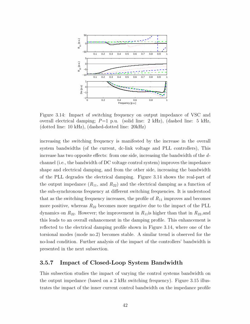
0.1 0.2 0.3 0.4 0.5 0.6 0.7 0.8 0.9 1−50
0
50
R11
(p.
u.)
0.1 0.2 0.3 0.4 0.5 0.6 0.7 0.8 0.9 1−10
−5
0
5
R22
(p.
u.)
0 0.2 0.4 0.6 0.8 1−2
−1
0
1D
e (p
.u)
Frequency [p.u.]
Figure 3.14: Impact of switching frequency on output impedance of VSC andoverall electrical damping; P=1 p.u. (solid line: 2 kHz), (dashed line: 5 kHz,(dotted line: 10 kHz), (dashed-dotted line: 20kHz)
increasing the switching frequency is manifested by the increase in the overall
system bandwidths (of the current, dc-link voltage and PLL controllers), This
increase has two opposite effects: from one side, increasing the bandwidth of the d -
channel (i.e., the bandwidth of DC voltage control system) improves the impedance
shape and electrical damping, and from the other side, increasing the bandwidth
of the PLL degrades the electrical damping. Figure 3.14 shows the real-part of
the output impedance (R11, and R22) and the electrical damping as a function of
the sub-synchronous frequency at different switching frequencies. It is understood
that as the switching frequency increases, the profile of R11 improves and becomes
more positive, whereas R22 becomes more negative due to the impact of the PLL
dynamics on R22. However; the improvement in R11is higher than that in R22,and
this leads to an overall enhancement in the damping profile. This enhancement is
reflected to the electrical damping profile shown in Figure 3.14, where one of the
torsional modes (mode no.2) becomes stable. A similar trend is observed for the
no-load condition. Further analysis of the impact of the controllers’ bandwidth is
presented in the next subsection.
3.5.7 Impact of Closed-Loop System Bandwidth
This subsection studies the impact of varying the control systems bandwidth on
the output impedance (based on a 2 kHz switching frequency). Figure 3.15 illus-
trates the impact of the inner current control bandwidth on the impedance profile
42

0.1 0.2 0.3 0.4 0.5 0.6 0.7 0.8 0.9 1
0
0.5
1
Rcc
(p.
u)
0.1 0.2 0.3 0.4 0.5 0.6 0.7 0.8 0.9 1−10
0
10
R11
(p.
u)
0.1 0.2 0.3 0.4 0.5 0.6 0.7 0.8 0.9 1−10
−5
0
Frequency [p.u.]
R22
(p.
u.)
ωcc
= 10% ωcc
= 15% ωcc
= 20%
Figure 3.15: Impact of current-control system bandwidth on output impedanceelements: Zcc, Z 11 and Z 22.
for three ranges (10, 15, and 20% of the switching frequency) while keeping the
bandwidth of the outer loop as 10%, under the dc-voltage controller and UPF
control scheme. It is clear that fast current control (i.e., the high bandwidth) has
a positive impact on Z 11 in the low-frequency ranges and negative impact in the
high-frequency ranges, and also has a negative impact on Z 22. Therefore, the use of
the higher current bandwidth is recommended to maximize the positive impedance
and minimize the negative interaction at sub-synchronous frequencies. A higher
current controller bandwidth can be achieved at a fixed switching frequency by us-
ing the double switching frequency sampling rate and/or using field-programmable
gate arrays to eliminate the calculation delay associated with digital implementa-
tion.
Figure 3.16 shows the effect of the bandwidth of the outer loops (dc-link voltage
controller and PLL controller) on the impedance profile for three ranges (10, 15,
and 20% of that of the current controller) whereas there is no change in the other
controllers’ bandwidths. The dc-link voltage controller affects only Z 11, whereas
the PLL loop affects only Z 22. It is observed that as the dc-link voltage control
bandwidth increases, the positive resistance at low frequencies increases, whereas
increasing the control bandwidth increases the negative resistance region at the
high-frequency range.It is understood that a fast PLL would increase the area of
the negative resistance. The choice of the bandwidth for the PLL depends on its
application: the bandwidth of a PLL used for synchronization and transformation
43
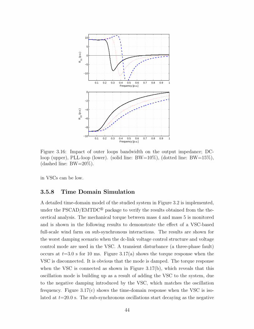
0.1 0.2 0.3 0.4 0.5 0.6 0.7 0.8 0.9 1
−10
−5
0
5
10
Frequency [p.u.]
R11
(p.
u.)
0.1 0.2 0.3 0.4 0.5 0.6 0.7 0.8 0.9 1−10
−8
−6
−4
−2
0
Frequency [p.u.]
R22
(p.
u.)
Figure 3.16: Impact of outer loops bandwidth on the output impedance; DC-loop (upper), PLL-loop (lower). (solid line: BW=10%), (dotted line: BW=15%),(dashed line: BW=20%).
in VSCs can be low.
3.5.8 Time Domain Simulation
A detailed time-domain model of the studied system in Figure 3.2 is implemented,
under the PSCAD/EMTDCr package to verify the results obtained from the the-
oretical analysis. The mechanical torque between mass 4 and mass 5 is monitored
and is shown in the following results to demonstrate the effect of a VSC-based
full-scale wind farm on sub-synchronous interactions. The results are shown for
the worst damping scenario when the dc-link voltage control structure and voltage
control mode are used in the VSC. A transient disturbance (a three-phase fault)
occurs at t=3.0 s for 10 ms. Figure 3.17(a) shows the torque response when the
VSC is disconnected. It is obvious that the mode is damped. The torque response
when the VSC is connected as shown in Figure 3.17(b), which reveals that this
oscillation mode is building up as a result of adding the VSC to the system, due
to the negative damping introduced by the VSC, which matches the oscillation
frequency. Figure 3.17(c) shows the time-domain response when the VSC is iso-
lated at t=20.0 s. The sub-synchronous oscillations start decaying as the negative
44
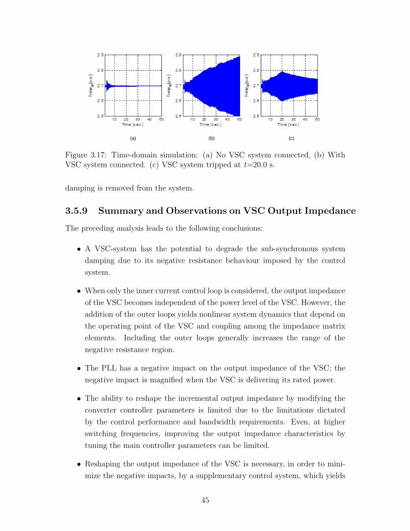
(a) (b) (c)
Figure 3.17: Time-domain simulation: (a) No VSC system connected, (b) WithVSC system connected. (c) VSC system tripped at t=20.0 s.
damping is removed from the system.
3.5.9 Summary and Observations on VSC Output Impedance
The preceding analysis leads to the following conclusions:
• A VSC-system has the potential to degrade the sub-synchronous system
damping due to its negative resistance behaviour imposed by the control
system.
• When only the inner current control loop is considered, the output impedance
of the VSC becomes independent of the power level of the VSC. However, the
addition of the outer loops yields nonlinear system dynamics that depend on
the operating point of the VSC and coupling among the impedance matrix
elements. Including the outer loops generally increases the range of the
negative resistance region.
• The PLL has a negative impact on the output impedance of the VSC; the
negative impact is magnified when the VSC is delivering its rated power.
• The ability to reshape the incremental output impedance by modifying the
converter controller parameters is limited due to the limitations dictated
by the control performance and bandwidth requirements. Even, at higher
switching frequencies, improving the output impedance characteristics by
tuning the main controller parameters can be limited.
• Reshaping the output impedance of the VSC is necessary, in order to mini-
mize the negative impacts, by a supplementary control system, which yields
45

a second-degree-of-freedom to reshape the converter impedance with a min-
imum effect on the closed-loop control performance (the tracking and dis-
turbance rejection). Furthermore, the reshaping technique should be robust
against the variation in the operating point, and, it should also offer a simple
structure and easy tuning process. Motivated by these limitations, this thesis
proposes several reshaping techniques to satisfy the above design objectives.
These techniques are discussed in the following chapter.
46

Chapter 4
Mitigation Techniques via ActiveDamping Controllers 3
Based on the preceding analysis, a remedial action is needed to minimize the neg-
ative resistance introduced by the VSC and avoid possible instability. The use of
the control system parameters to reshape the output impedance of VSC is limited
by the control performance and bandwidth requirements. Therefore, supplementary
compensation techniques are required to minimize the negative impact. Passive
compensation can also be achieved by adding passive elements (e.g., resistors);
however, this approach is impractical in high-power systems application due to
the additional losses and the unrealistically large size of the required damping re-
sistor. Active damping technique involves modifying the control system without
affecting the system efficiency and stability. Accordingly, active damping compen-
sation methods are proposed in this chapter to reshape the output impedance and
minimize the negative resistance region to avoid possible negative sub-synchronous
interactions. In this chapter, three active damping methods are proposed.
4.1 Active Damping Scheme No. 1 (DC Loop-
Based Active Damping Controller )
The structure of the first proposed active compensation is illustrated in Figure 4.1.
Its basic concept is based on using the grid voltage (the direct component) to in-
ject a transient component into the outer dc-voltage control loop. This approach
creates additional active impedance that can be used and controlled to reshape
the overall VSC impedance to increase the overall system damping in the sub-
synchronous frequency range. The active damping signal is generated by process-
3 This work is publised in IEEE Transaction on Power Electronics [69].
47

2ref
dcV-+
2
dcVwP PH
- )(ˆ
1
gvg VHV
gV vH
ref
di
dcC ++
gdv)(sB
Active damping
Figure 4.1: Proposed active damping scheme no. 1.
ing the grid voltage by a band-pass filter (B(s)). The zero-dc-gain of the filter
guarantees that the added damping controller does not yield steady-state errors in
the dc-voltage control loop.
The new transfer function that relates the change in current reference to the
change in the grid voltage with the proposed active damping controller can be
expressed as
∆iref(d−new) = T1∆vgd + T2∆vgq +G(s)∆vgd, (4.1)
G(s) =B(s)Gdc(s)
H(s), (4.2)
where
B(s) =k(2ζωcs)
(s2 + 2sζωc + ω2c ).
Under a unity power factor mode, the dc-loop dynamics impacts the Y 11(s) ele-
ment, which is expressed as
Y11 (s) = ycc (s) −f cc (s)T 1(s) (4.3)
where
T1(s) =
{[po − po + Zcc
−1]Cdc(s)
(sC + Cdc(s))+ po
}.
It is obvious that the worst case scenario occurs under no-load (or light-load),
leading to a simplified expression of the contribution of dc-controller as
T1 =ycc(s)Cdc(s)
(sC + Cdc(s)). (4.4)
48
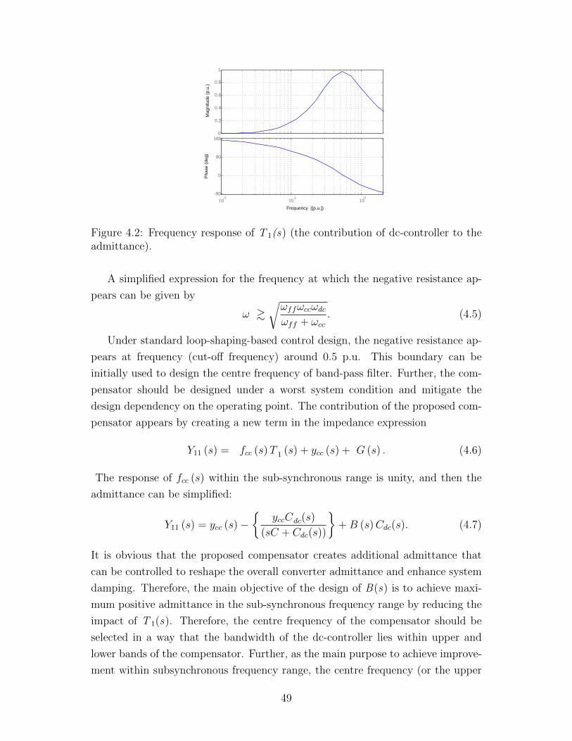
0
0.2
0.4
0.6
0.8
1
Ma
gn
itu
de
(p
.u.)
10-2
10-1
100
-90
0
90
180
Ph
ase
(d
eg
)Frequency ([p.u.])
Figure 4.2: Frequency response of T 1(s) (the contribution of dc-controller to theadmittance).
A simplified expression for the frequency at which the negative resistance ap-
pears can be given by
ω &√ωffωccωdcωff + ωcc
. (4.5)
Under standard loop-shaping-based control design, the negative resistance ap-
pears at frequency (cut-off frequency) around 0.5 p.u. This boundary can be
initially used to design the centre frequency of band-pass filter. Further, the com-
pensator should be designed under a worst system condition and mitigate the
design dependency on the operating point. The contribution of the proposed com-
pensator appears by creating a new term in the impedance expression
Y11 (s) = fcc (s)T 1 (s) + ycc (s) + G (s) . (4.6)
The response of fcc (s) within the sub-synchronous range is unity, and then the
admittance can be simplified:
Y11 (s) = ycc (s)−{
yccCdc(s)
(sC + Cdc(s))
}+B (s)Cdc(s). (4.7)
It is obvious that the proposed compensator creates additional admittance that
can be controlled to reshape the overall converter admittance and enhance system
damping. Therefore, the main objective of the design of B(s) is to achieve maxi-
mum positive admittance in the sub-synchronous frequency range by reducing the
impact of T 1(s). Therefore, the centre frequency of the compensator should be
selected in a way that the bandwidth of the dc-controller lies within upper and
lower bands of the compensator. Further, as the main purpose to achieve improve-
ment within subsynchronous frequency range, the centre frequency (or the upper
49
frequency limit) of compensator should be limited to fundamental frequency ( i.e.,
ωc < ωo ). Figure 4.2 shows the frequency response of T 1(s) (i.e., the contri-
bution of dc-link to the output admittance), where the impact of the dc-link is
maximum at higher frequency.The gain of the compensator k should be limited
to small vaule, as a higher gain tends to make the dc-link voltage more sensitive
to grid disturbance, and negatively impact the control performance. Therefore,
selecting the gain is a trade-off between the damping effect and the impact on
the system dynamic and control performance. Accordingly, using the aforemen-
tioned boundary and to minimize the impact of dc-controller, the following pa-
rameters are used ζ = 1.0, ωc = 0.8 p.u. and k = 0.8 p.u. . By using the modified
impedance(admittance) elements in (4.1), the new overall impedance expression
can be obtained
As the injection point of the active damping is located in the dc-link volt-
age control loop, two impedance elements are affected: Z11, and Z21. Figure 4.3
compares the profiles of Z 11 and Z 21 with and without the compensation. It is ob-
served that the compensation remarkably improves Z 11, and a positive impedance
is achieved in all the sub-synchronous range, whereas without compensation, the
positive impedance occurs only when (f >0.7 p.u.), also the level of the positive
resistance is boosted. The proposed technique also improves the profile of Z 21.
The positive impedance appears when (f >0.8 p.u.), whereas a negative resistance
in all the frequencies appears in the uncompensated case.
To study the effectiveness of the proposed technique on the overall system elec-
trical damping profile, the profiles of the overall electrical damping are obtained
with and without compensation, for the three operational modes: the unity power
factor, V-mode and the Q-mode with a dc-link voltage controller (i.e., Vdc-UPF,
Vdc-V, and Vdc-Q modes), (see Figure 4.4 ). It is clear that the proposed active
compensation improves the electrical damping in the entire sub-synchronous range.
Such improvement is expected as the impedance profile shows a considerable im-
provement under the proposed active damping method.
4.1.1 Time-Domain Simulations
A detailed time-domain model of the studied system in Figure 3.2 is implemented,
under the PSCAD/EMTDCr package to verify the theoretical damping analysis.
The mechanical torque between mass 4 and mass 5 and between the exciter and
generator was monitored and is shown in the following results to demonstrate the
effect of a full-scale VSC-based wind-farm on the sub-synchronous damping and
50

0
5
10
15
20M
agni
tude
(p.
u.)
0.2 0.4 0.6 0.8 1 1.2 1.4 1.6 1.8 2−450
−360
−270
−180
−90
0
Pha
se (
deg)
Frequency ([p.u.])
(a)
0
2
4
6
8
10
Mag
nitu
de (
p.u.
)
0.2 0.4 0.6 0.8 1 1.2 1.4 1.6 1.8 2−225
−180
−135
−90
−45
0
Pha
se (
deg)
Frequency ([p.u.])
(b)
Figure 4.3: Output impedance (solid line: uncompensated), (dotted line: compen-sated) (a) Z 11, (b) Z 21.
51

0 0.1 0.2 0.3 0.4 0.5 0.6 0.7 0.8 0.9 1−2
−1
0
1
2
De
(p.u
.)
Frequency [p.u.]
(a)
0 0.2 0.4 0.6 0.8 1−3
−2
−1
0
1
2
De
(p.u
.)
Frequency [p.u.]
(b)
0 0.1 0.2 0.3 0.4 0.5 0.6 0.7 0.8 0.9 1−3
−2
−1
0
1
2
3
De
(p.u
.)
Frequency [p.u.]
(c)
Figure 4.4: Electrical damping. (solid line: uncompensated), (dotted line: com-pensated). (a) Vdc-UPF scheme, (b)Vdc-V scheme, (c)Vdc-Q scheme.
2 3 4 5 6 7 82.64
2.66
2.68
2.7
2.72
2.74
Tor
que
4−5[p
.u.]
2 3 4 5 6 7 80.196
0.198
0.2
0.202
Time [sec.]
Tor
que
EX
E−
GE
N[p
.u.]
Figure 4.5: Time-domain simulation without VSC system connected.
52

2 3 4 5 6 7 82.64
2.66
2.68
2.7
2.72
2.74
Tor
que
4−5[p
.u.]
2 3 4 5 6 7 80.196
0.198
0.2
0.202
Time [sec.]
Tor
que
EX
E−
GE
N[p
.u.]
Figure 4.6: Time-domain simulation with VSC system connected (unity power-factor mode).
2 3 4 5 6 7 82.64
2.66
2.68
2.7
2.72
2.74
Tor
que
4−5[p
.u.]
2 3 4 5 6 7 80.196
0.198
0.2
0.202
Time [sec.]
Tor
que
EX
E−
GE
N[p
.u.]
Figure 4.7: Time-domain simulation with compensated VSC system (unity powerfactor mode).
2 3 4 5 6 7 82.64
2.66
2.68
2.7
2.72
2.74
Tor
que
4−5[p
.u.]
2 3 4 5 6 7 80.196
0.198
0.2
0.202
Time [sec.]
Tor
que
EX
E−
GE
N[p
.u.]
Figure 4.8: Time-domain simulation with VSC system connected (reactive powerinjection-mode).
53

2 3 4 5 6 7 82.64
2.66
2.68
2.7
2.72
2.74
Tor
que
4−5[p
.u.]
2 3 4 5 6 7 80.196
0.198
0.2
0.202
Time [sec.]
Tor
que
EX
E−
GE
N[p
.u.]
Figure 4.9: Time-domain simulation with compensated VSC system (reactivepower injection-mode).
2 3 4 5 6 7 82.64
2.66
2.68
2.7
2.72
2.74
Tor
que
4−5[p
.u.]
2 3 4 5 6 7 80.196
0.198
0.2
0.202
Time [sec.]
Tor
que
EX
E−
GE
N[p
.u.]
Figure 4.10: Time-domain simulation with VSC system connected (ac-voltagecontrol-mode).
2 3 4 5 6 7 82.64
2.66
2.68
2.7
2.72
2.74
Tor
que
4−5[p
.u.]
2 3 4 5 6 7 80.196
0.198
0.2
0.202
Time [sec.]
Tor
que
EX
E−
GE
N[p
.u.]
Figure 4.11: Time-domain simulation with compensated VSC system (ac-voltagecontrol-mode).
54
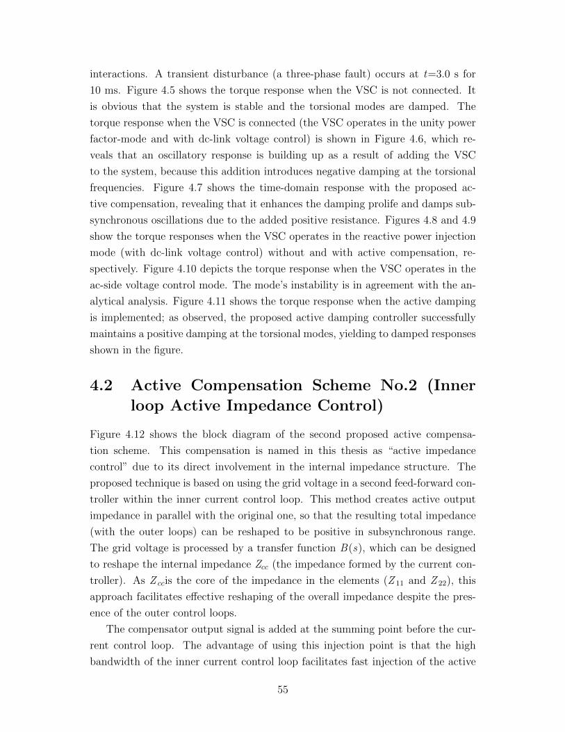
interactions. A transient disturbance (a three-phase fault) occurs at t=3.0 s for
10 ms. Figure 4.5 shows the torque response when the VSC is not connected. It
is obvious that the system is stable and the torsional modes are damped. The
torque response when the VSC is connected (the VSC operates in the unity power
factor-mode and with dc-link voltage control) is shown in Figure 4.6, which re-
veals that an oscillatory response is building up as a result of adding the VSC
to the system, because this addition introduces negative damping at the torsional
frequencies. Figure 4.7 shows the time-domain response with the proposed ac-
tive compensation, revealing that it enhances the damping prolife and damps sub-
synchronous oscillations due to the added positive resistance. Figures 4.8 and 4.9
show the torque responses when the VSC operates in the reactive power injection
mode (with dc-link voltage control) without and with active compensation, re-
spectively. Figure 4.10 depicts the torque response when the VSC operates in the
ac-side voltage control mode. The mode’s instability is in agreement with the an-
alytical analysis. Figure 4.11 shows the torque response when the active damping
is implemented; as observed, the proposed active damping controller successfully
maintains a positive damping at the torsional modes, yielding to damped responses
shown in the figure.
4.2 Active Compensation Scheme No.2 (Inner
loop Active Impedance Control)
Figure 4.12 shows the block diagram of the second proposed active compensa-
tion scheme. This compensation is named in this thesis as “active impedance
control” due to its direct involvement in the internal impedance structure. The
proposed technique is based on using the grid voltage in a second feed-forward con-
troller within the inner current control loop. This method creates active output
impedance in parallel with the original one, so that the resulting total impedance
(with the outer loops) can be reshaped to be positive in subsynchronous range.
The grid voltage is processed by a transfer function B(s), which can be designed
to reshape the internal impedance Zcc (the impedance formed by the current con-
troller). As Z ccis the core of the impedance in the elements (Z 11 and Z 22), this
approach facilitates effective reshaping of the overall impedance despite the pres-
ence of the outer control loops.
The compensator output signal is added at the summing point before the cur-
rent control loop. The advantage of using this injection point is that the high
bandwidth of the inner current control loop facilitates fast injection of the active
55

-- ++ i
p
kk
s
ff
ffs
1
Ls R
FF(s)
1/L(s)Ccc(s) Converter(VSC)
Grid Dynamics
ig
vg
iref ++
( )B s
Active impedance controller
+
Converter Dynamics
Figure 4.12: Output impedance of current controller(Zcc), with and without activeimpedance control.
damping signal, which shapes the converter impedance. The modified transfer
functions of the current controller and internal-impedance with the proposed ac-
tive impedance controller can be expressed as
ig =Ccc(s)
(L(s) + Ccc(s))iref +
[1−H(s) +B(s)Ccc(s)]
[L(s) + Ccc(s)]vg, (4.8)
where
B(s) =k(2ζωcs)
(s2 + 2sζωc + ω2c ). (4.9)
The new impedance expression is given by
ZNewcc =
s(s+ ωff )(s2 + 2sζωc + ω2
c )− sωff + 2skζωc(kps+ ki)(s+ ωff ))
s(s2 + 2sζωc + ω2c )(s+ ωff )(Ls2 + kps+ ki))
.
(4.10)
The selection of the compensator B(s) depends on the dynamics needed to reshape
the output impedance in the presence of the outer loops. Basically, the compen-
sation should operate only in transient conditions without affecting the tracking
performance as demonstrated in (4.8). The compensator B(s) is chosen such that
the negative resistance that appears in the low -frequency region can be either
minimized or eliminated. To meet these design objectives, B(s) can be designed
as a band-pass filter, which yields a zero-dc-gain and facilitates the shaping of the
incremental output impedance around a center frequency. The following guidelines
can be used to design the compensator:
• The effective frequency range of the compensation is only to compensate
the area where the negative resistance exist i.e., ωn <√
ωffkikp+R+Lωff
(cut-off
56

frequency of the negative resistance. ). As a band-pass filter gives the maxi-
mum compensation (and here maximum positive resistance) around its centre
frequency, ωc,(between its upper and lower cutoff frequencies), therefore, in
order to maximize the effect of the compensation,the selection of ωc, should
be limited to cut-off frequency of the negative resistance. (i.e., 0 < ωc ≤ ωn).
It is found that the optimal location is ωc = ωn =√
ωffkikp+R+Lωff
.
• The design parameters for the compensation are also limited by additional
burden added to the disturbance rejection capability of the converter. Com-
pensation with high centre frequency yields a better disturbance rejection
capability. Further, the gain of the compensator should be limited to a small
vaule, as a higher gain tends to increase and make the converter current more
sensitive to the grid disturbance, and negatively impact the disturbance re-
jection capability performance. Therefore, selecting the gain is a trade-off
between the needed damping level and the impact on the converter dynamics
dynamic. Therefore, in order to minimize the impact of proposed damping,
the mid-band gain need to chosen as small as possible.
By following the above design limitations and guidelines, the parameters of B(s)
are chosen as ζ=1, ωc=0.2 p.u.and kc=1 to increase the positive resistance. By
using the modified expressions of internal impedance in (4.9), the overall impedance
and the electrical damping of the system can be obtained.
Figure 4.13 shows the frequency response of the internal impedance Zcc with
and without active compensation at different values of ωc. As this figure reveals,
the output impedance becomes positive in the entire sub-synchronous range. Fig-
ure 4.14 shows the corresponding overall system damping profile along with the re-
sistive parts of the output impedances elements Z 11, Z 22 and Zcc with and without
active compensation. Figure 4.14 reveals also that the internal output resistance
(Rcc) becomes positive in the entire sub-synchronous range, according to the profile
of Z 11 and Z22 (the complete impedance elements with outer loops and PLL) are
improved. For R11, adding the active damping increases the positive region of the
output impedance and brings the positive resistance at lower frequency as it ap-
pears at f=0.5 p.u. instead of at f=0.73 p.u. in the uncompensated case. Similarly
for R22, the positive resistance appears at f=0.65 p.u. as compared to f=0.9p.u.
in the uncompensated case.With this improvement the electrical damping is ob-
tained and shown in the bottom of the figure. The effectiveness of the proposed
active impedance control scheme was tested under different output power levels
of the VSC (i.e., from no-load to full-load conditions). The resulting electrical
57

0
1
2
3
4
5
6
Mag
nitu
de (
p.u.
)
0.2 0.4 0.6 0.8 1 1.2 1.4 1.6 1.8 2−180
−135
−90
−45
0
45
Pha
se (
deg)
Frequency ([p.u.])
Uncomp
ωc=0.3
ωc=0.5
ωc=.75
ωc=1.0
Figure 4.13: Output impedance of current controller (Zcc), with and without activeimpedance control.
0.1 0.2 0.3 0.4 0.5 0.6 0.7 0.8 0.9 1−0.5
0
0.5
1
1.5
Rcc
(p.
u.)
0.1 0.2 0.3 0.4 0.5 0.6 0.7 0.8 0.9 1
−2
0
2
R11
(p.
u.)
0.1 0.2 0.3 0.4 0.5 0.6 0.7 0.8 0.9 1
−2
0
2
Frequency [p.u.]
R22
(p.
.)
0 0.1 0.2 0.3 0.4 0.5 0.6 0.7 0.8 0.9 1−1
−0.5
0
0.5
De(
p.u.
)
Frequency [p.u.]
Figure 4.14: Output impedance and electrical damping (solid line: uncompen-sated), (dotted line: compensated), at P=1.0 p.u.
58
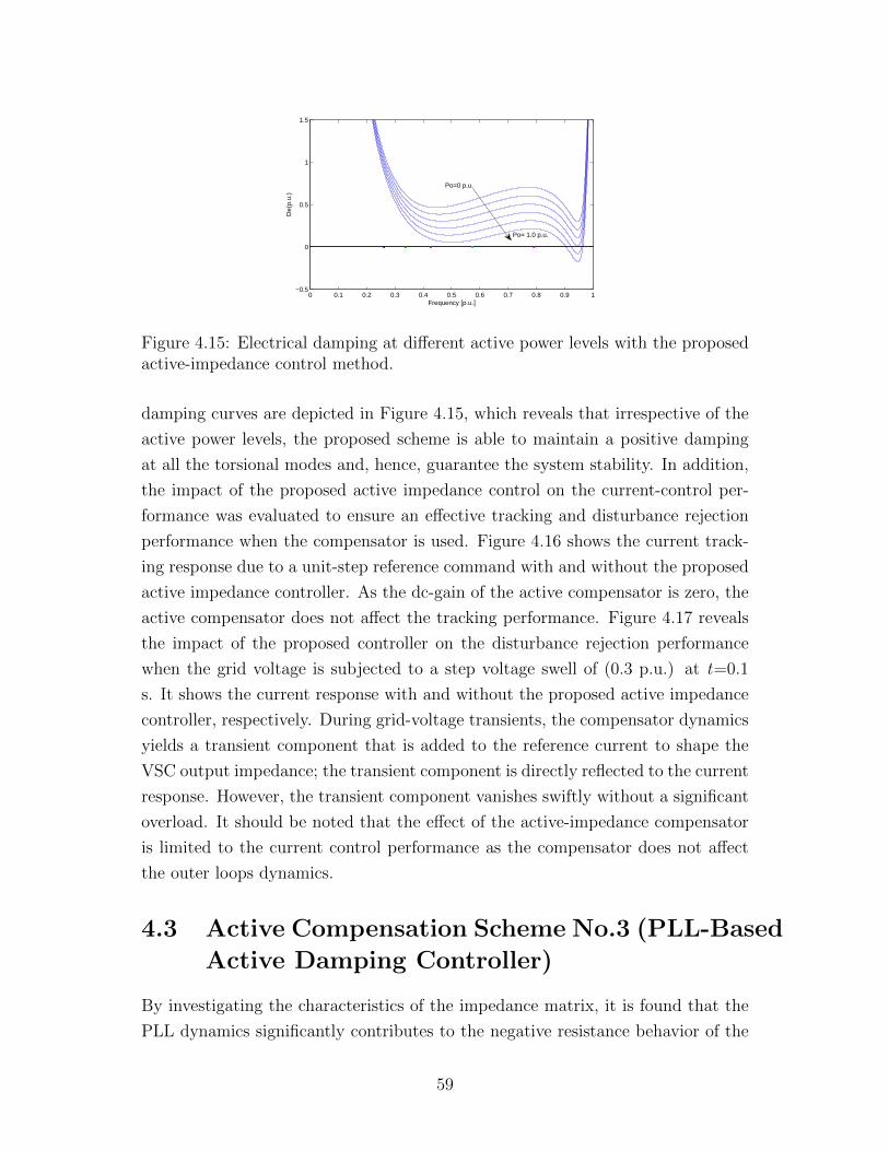
0 0.1 0.2 0.3 0.4 0.5 0.6 0.7 0.8 0.9 1−0.5
0
0.5
1
1.5
De(
p.u.
)
Frequency [p.u.]
Po=0 p.u.
Po= 1.0 p.u.
Figure 4.15: Electrical damping at different active power levels with the proposedactive-impedance control method.
damping curves are depicted in Figure 4.15, which reveals that irrespective of the
active power levels, the proposed scheme is able to maintain a positive damping
at all the torsional modes and, hence, guarantee the system stability. In addition,
the impact of the proposed active impedance control on the current-control per-
formance was evaluated to ensure an effective tracking and disturbance rejection
performance when the compensator is used. Figure 4.16 shows the current track-
ing response due to a unit-step reference command with and without the proposed
active impedance controller. As the dc-gain of the active compensator is zero, the
active compensator does not affect the tracking performance. Figure 4.17 reveals
the impact of the proposed controller on the disturbance rejection performance
when the grid voltage is subjected to a step voltage swell of (0.3 p.u.) at t=0.1
s. It shows the current response with and without the proposed active impedance
controller, respectively. During grid-voltage transients, the compensator dynamics
yields a transient component that is added to the reference current to shape the
VSC output impedance; the transient component is directly reflected to the current
response. However, the transient component vanishes swiftly without a significant
overload. It should be noted that the effect of the active-impedance compensator
is limited to the current control performance as the compensator does not affect
the outer loops dynamics.
4.3 Active Compensation Scheme No.3 (PLL-Based
Active Damping Controller)
By investigating the characteristics of the impedance matrix, it is found that the
PLL dynamics significantly contributes to the negative resistance behavior of the
59

1 1.002 1.004 1.006 1.008 1.010
0.2
0.4
0.6
0.8
1
Time [s]
Cur
rent
ste
p re
spon
se
Figure 4.16: Tracking response of closed loop current controller with and withoutcompensation. (dashed: without proposed active impedance control) (dotted: withproposed active impedance control).
Figure 4.17: Current control performance (a) with proposed active impedancecontrol (b) without proposed active impedance control
60

VSC at sub-synchronous frequencies, especially at the high output power levels of
the VSC. Thus, an improvement in the PLL dynamics can lead to an improvement
in the overall impedance and hence, in the electrical damping. Accordingly, the
output impedance can be actively reshaped by modifying the PLL control loop
dynamics by using an active damping controller within the PLL structure and
bandwidth . The purpose of the active damping controller is to minimize the
effect of the PLL in the high-frequency rang of the sub-synchronous range while
maintaining the desirable tracking characteristics of the PLL. These objectives
can be met by introducing a notch filter within the PLL dynamics to reshape the
loop gain and improve the the converter impedance within the sub-synchronous
frequency range. Figure 4.18 illustrates the small-signal model of the PLL loop
with the proposed active compensation. Using Figure 4.18, the modified closed-
loop PLL dynamics can be given by
GnewPLL(s) =
CPLL(s)
(s+ [ G(s)(1+G(s))
] + vogCPLL(s), (4.11)
where G(s) is a notch filter given by
G(s) = kc(2ζωcs)
(s2 + 2sζωc + ω2c ). (4.12)
The PLL dynamics affects the Y 22 element, which is expressed as
Y22 (s) = ycc (s) (1− GnewPLL(s))− P oGnew
PLL(s). (4.13)
It is clear that the worst case scenario occur under a loaded condition, where under
rated power
→ Y 22 (s) = ycc (s) (1− GnewPLL(s))−Gnew
PLL(s). (4.14)
The basic target of the added compensator is to achieve Re{Y 22 (s)} > 0, however,
this condition cannot be satisfied by compensation. Instead, the design parame-
ters of G(s) can be tuned to reduce the contribution of the PLL to the quadratic
impedance channel and to minimize the negative resistance of Y22.. AS the modi-
fication is implemented within the PLL, the centre frequency should be lower than
that the bandwidth of the PLL. The selection of the parameters is also limited by
the bandwidth and response of PLL. As the loop modification should not violate
the system response. Accordingly, the following parameters are used: ζ=0.707,
ωn=0.055 p.u. and k=1.0
Using the resultant impedance expression with the modified PLL dynamics,
Figure 4.19 shows the electrical damping along with the real-part of Z 22 (R22),
61

-
c+ ˆ
gV
g 1
s-+
-+
( )PLLC s
( )G s
Comp.
Figure 4.18: Small signal model of the proposed PLL-based active damping con-troller.
0 0.2 0.4 0.6 0.8 1−1
0
1
2
De
(p.u
.)
0.1 0.2 0.3 0.4 0.5 0.6 0.7 0.8 0.9 1−1
−0.5
0
0.5
1
Frequency [p.u.]
R22
(p.
u.)
Figure 4.19: Electrical damping and R22 profiles at P=1.0 p.u. with and with-out proposed PLL-based active damping controller. (solid line: uncompensated),(dotted line: compensated)
62
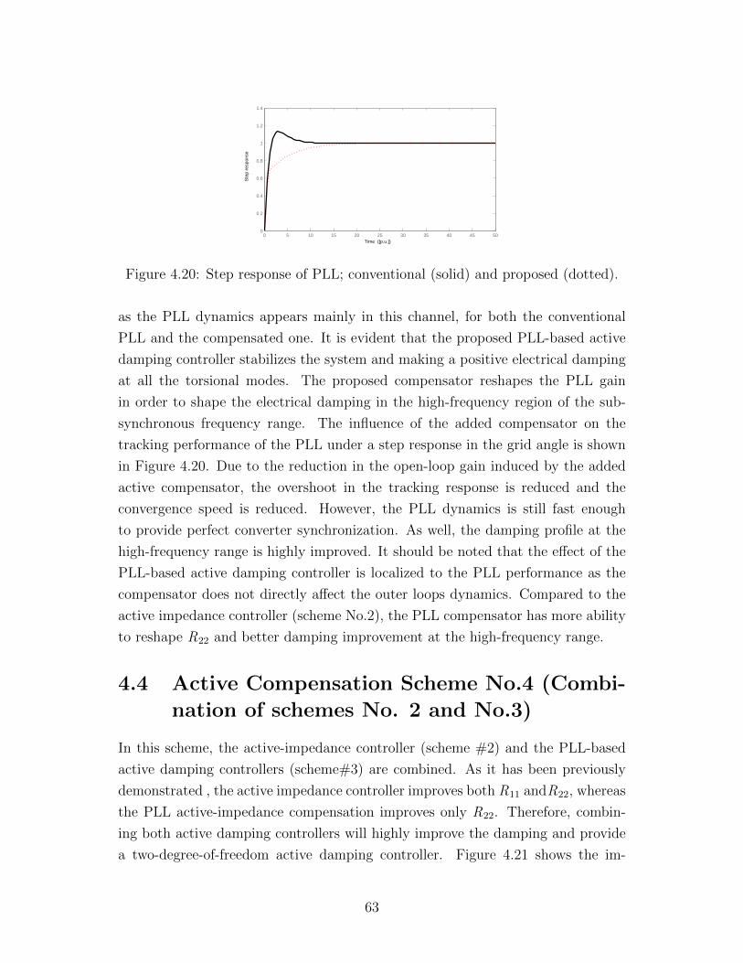
0 5 10 15 20 25 30 35 40 45 500
0.2
0.4
0.6
0.8
1
1.2
1.4
Time ([p.u.])S
tep
resp
onse
Figure 4.20: Step response of PLL; conventional (solid) and proposed (dotted).
as the PLL dynamics appears mainly in this channel, for both the conventional
PLL and the compensated one. It is evident that the proposed PLL-based active
damping controller stabilizes the system and making a positive electrical damping
at all the torsional modes. The proposed compensator reshapes the PLL gain
in order to shape the electrical damping in the high-frequency region of the sub-
synchronous frequency range. The influence of the added compensator on the
tracking performance of the PLL under a step response in the grid angle is shown
in Figure 4.20. Due to the reduction in the open-loop gain induced by the added
active compensator, the overshoot in the tracking response is reduced and the
convergence speed is reduced. However, the PLL dynamics is still fast enough
to provide perfect converter synchronization. As well, the damping profile at the
high-frequency range is highly improved. It should be noted that the effect of the
PLL-based active damping controller is localized to the PLL performance as the
compensator does not directly affect the outer loops dynamics. Compared to the
active impedance controller (scheme No.2), the PLL compensator has more ability
to reshape R22 and better damping improvement at the high-frequency range.
4.4 Active Compensation Scheme No.4 (Combi-
nation of schemes No. 2 and No.3)
In this scheme, the active-impedance controller (scheme #2) and the PLL-based
active damping controllers (scheme#3) are combined. As it has been previously
demonstrated , the active impedance controller improves both R11 andR22, whereas
the PLL active-impedance compensation improves only R22. Therefore, combin-
ing both active damping controllers will highly improve the damping and provide
a two-degree-of-freedom active damping controller. Figure 4.21 shows the im-
63

provement in the output impedance profile under the proposed active damping
schemes for no-load and full-load conditions, respectively. These figures clearly
show that combining the two schemes yields a better performance in both no-load
and full-load cases. The corresponding damping profiles are shown in Figure 4.22
for the no-load and full-load, respectively. It is evident that the proposed active
damping successfully improves the electrical damping and eventually stabilizes all
the torsional modes. Figure 4.23 shows the robustness of the combined scheme
against variation in the active power operation point. An excellent improvement
is achieved as the proposed combined compensator makes the output impedance
almost independent of the active-power operating point. This result significantly
contributes to the robustness of the stability margins at different operating points
of the VSC.
4.4.1 Time-Domain Simulation
A detailed time-domain model of the studied system in Figure 3.2 is implemented
under the PSCAD/EMTDCr environment to verify the theoretical analysis and
effectiveness of the proposed active mitigation schemes. The mechanical torque
between mass 4 and mass 5 is monitored and is shown in the following results to
demonstrate the effect of the VSC on sub-synchronous torsional oscillations. A
transient disturbance (a three-phase fault) occurs at t=8.0 s for 10 ms to excite
the system dynamics. Figure 4.24 shows the torque response when the VSC is
not connected (the base-case). The system is stable, and the torsional mode is
damped. The torque response when the uncompensated VSC is connected (with
control scheme 1) is shown in Figure 4.25(a). It is clear that the oscillation is
building up as a result of adding the VSC to the system (due to its negative
resistance), which introduces negative damping at the torsional frequencies. The
corresponding converter output current in this case is shown in Figure 4.25(b),
where the converter becomes unstable because it is driven by the system instability.
Figure 4.26 and 4.27 show the time-domain response (the mechanical torque
between mass 4 and 5, T45, and for the converter current) for a VSC with the
proposed active-impedance controller (scheme 2) and the combined PLL and ac-
tive impedance controllers (scheme 3), respectively. It is clearly shown that the
proposed active compensation techniques enhance the damping profile and damp
sub-synchronous oscillations.
64
0.1 0.2 0.3 0.4 0.5 0.6 0.7 0.8 0.9 1−10
−5
0
R11
(p.
u.)
0.1 0.2 0.3 0.4 0.5 0.6 0.7 0.8 0.9 1−10
−5
0
5
10
Frequency [p.u.]
R22
(p.
u.)
(a)
0.1 0.2 0.3 0.4 0.5 0.6 0.7 0.8 0.9 1−10
−5
0
R11
(p.
u.)
0.1 0.2 0.3 0.4 0.5 0.6 0.7 0.8 0.9 1−10
−5
0
5
10
Frequency [p.u.]
R22
(p.
u.)
(b)
Figure 4.21: Real-part of impedance elements with the proposed damping tech-niques: (a) full-load condition (P= 1.0 p.u.), (b) no-load condition (P= 0). (solidline: uncompensated), (dashed line: compensated with internal impedance method), (dotted line: compensated with PLL method), (dotted-dashed line: compensatedwith the combination).
65
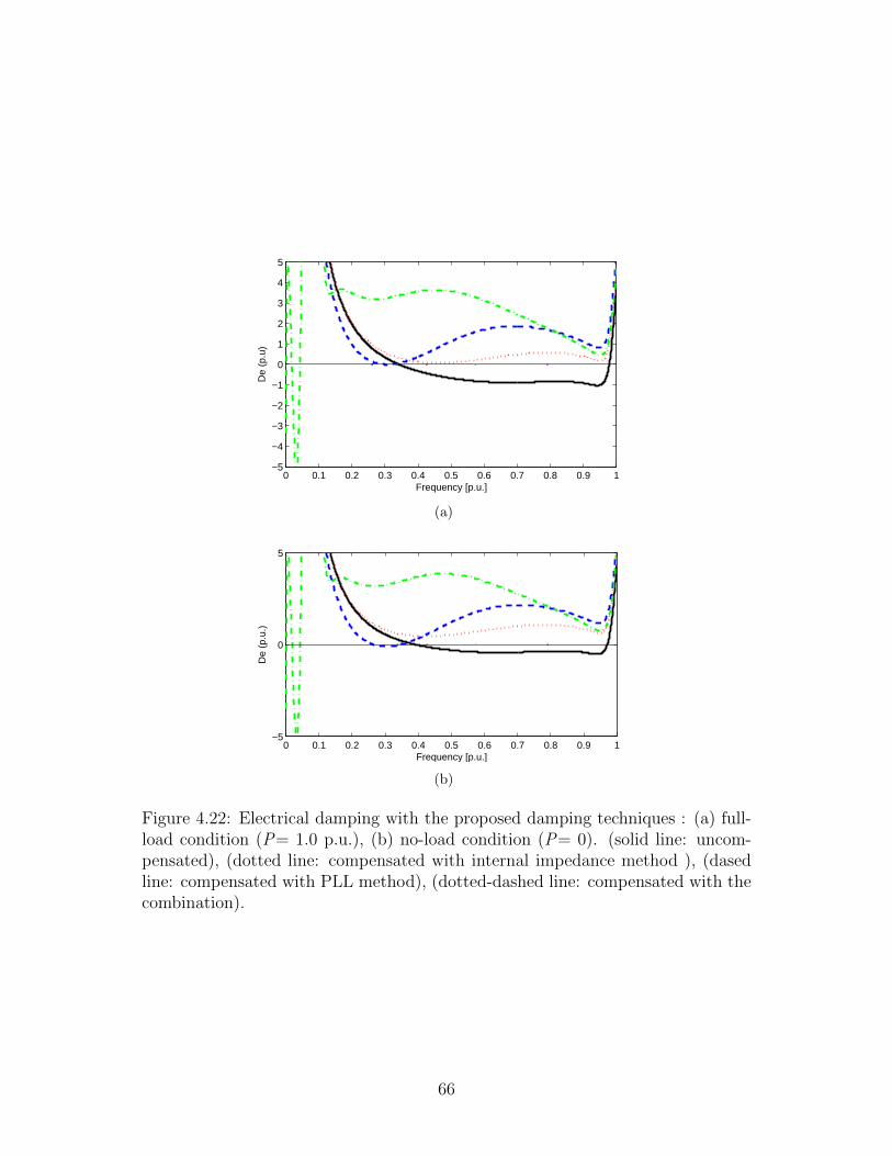
0 0.1 0.2 0.3 0.4 0.5 0.6 0.7 0.8 0.9 1−5
−4
−3
−2
−1
0
1
2
3
4
5D
e (p
.u)
Frequency [p.u.]
(a)
0 0.1 0.2 0.3 0.4 0.5 0.6 0.7 0.8 0.9 1−5
0
5
De
(p.u
.)
Frequency [p.u.]
(b)
Figure 4.22: Electrical damping with the proposed damping techniques : (a) full-load condition (P= 1.0 p.u.), (b) no-load condition (P= 0). (solid line: uncom-pensated), (dotted line: compensated with internal impedance method ), (dasedline: compensated with PLL method), (dotted-dashed line: compensated with thecombination).
66

0 0.1 0.2 0.3 0.4 0.5 0.6 0.7 0.8 0.9 1−5
0
5
De
(p.u
)
Frequency [p.u.]
Figure 4.23: Electrical damping with the proposed damping scheme no. 4: (solidline: P= 1.0 p.u.), (dotted line:P= 0).
Time [s] 7.5 10.0 12.5 15.0 17.5 20.0 ...
... ...
2.600
2.620
2.640
2.660
2.680
2.700
2.720
2.740
2.760
To
rqu
e (
pu)
T45
Figure 4.24: Time-domain simulation results- system without VSC connected.
(a)
(b)
Figure 4.25: Time-domain simulation results with uncompensated VSC systemconnected: (a) Mechanical torque T45, (b) Converter current waveforms.
67
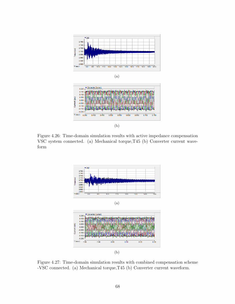
(a)
(b)
Figure 4.26: Time-domain simulation results with active impedance compensationVSC system connected. (a) Mechanical torque,T45 (b) Converter current wave-form
(a)
(b)
Figure 4.27: Time-domain simulation results with combined compensation scheme-VSC connected. (a) Mechanical torque,T45 (b) Converter current waveform.
68

PCCLg
C
L
LfGrid
Emulation of a torsional frequency
VSC-based system
Power system
Figure 4.28: Circuit diagram of system under the experimental test.
Figure 4.29: Picture of experimental setup and test components.
4.5 Experimental Results
An experimental test is performed to verify the effectiveness of the proposed active
damping techniques in mitigating possible sub-synchronous interactions between
a VSC and a power network. Figure 4.28 illustrates the circuit diagram used in
the experimental step. A Semikronr -Semistack intelligent power module, which
includes gate drives, six insulated-gate bipolar transistors (IGBTs), and protec-
tion circuit was used as a VSC connected to a 120 V (with auto-transformer),
60Hz grid via an inductor filter Lf=1.2 mH. A weak grid was emulated by con-
necting a 2.4mH series inductor between the grid and PCC. A parallel LC circuit
was connected at the PCC with (L=60 mH and C =250F) to emulate a torsional
frequency mode in the power network. With these parameters, a low-frequency
resonant mode at 41 Hz (0.68 p.u. on 60 Hz base-frequency) was obtained. Fig-
ure 4.29 shows the hardware set-up. The dc-link capacitor is Cdc=2040 F. The
VSC-side inductor currents were measured by HASS-50-S current sensors, and the
69

ac/dc voltage signals were measured by LEM-V-25-400 voltage sensors. The VSC
control scheme, dq orientation and the PWM generation were implemented on the
dSPACE1104 control card supported with a TMS320F240-DSP coprocessor struc-
ture for PWM generation. The dSPACE1104 interfacing board was equipped with
eight digital-to-analogue channels (DAC) and eight analogue-to-digital channels
(ADC) to interface the measured signals to/from the control system. The software
code was generated by the Real-Time-WorkShop under a Matlab/Simulink envi-
ronment. Several experimental tests were conducted. The key obtained results are
discussed in the following.
Figure 4.30 shows the experimental results when the VSC operates under the
Vdc and UPF control scheme and without an active damping control. Figure
shows the d -axis PCC voltage (Vd), converter current (id), and dc-link voltage
after activating the converter at t1=2s. This experimental test was performed when
the VSC was unloaded. As Figure 4.30 reveals, it is clear that the VSC induces
negative electrical damping, which yields to unstable sub-synchronous interactions
between the VSC and power network, when the network is disturbed by activating
the controlled VSC at t=2 s. The oscillations build up over a long period (18
s), which is the natural result of the low-frequency instability associated with sub-
synchronous frequencies. The converter voltage and current responses are unstable
with increasing magnitudes, as predicted by the theoretical analysis. The converter
instability is reflected to the dc-link voltage, which shows high ripple content even
at a low d-axis current. The dc-link voltage is not building up due to the large
size of the dc-link capacitor of the Semistack VSC module.
Figure 4.31 and 4.32 show the experimental results for the VSC with the pro-
posed active compensation scheme. Figures depict the experimental results of the
d-axis PCC voltage (Vd), converter d-axis current, id, and dc-link voltage after
activating the converter, at t=2 s for unloaded and full-load conditions; respec-
tively. It is evident that the active damping compensation stabilizes the system by
introducing positive electrical damping. In both the no-load and load conditions,
converter current and the control voltage are highly damped. The stable perfor-
mance of the converter current is reflected to the dc-link voltage, which shows
stable performance with reduced ripple-content as compared to the uncompen-
sated case. The proposed active damping controllers yield a robust performance
at different output power levels of the VSC.
70

[sec.]Time
[.
.]d
Vp
u
0.2 . /
2 /
p u div
s divConverter
start-up
0
1t
(a)
(b)
[.
.]dc
Vp
u
0.16 . /
2s /
p u div
div
(c)
Figure 4.30: Experimental results for unloaded VSC without active damping com-pensation. (a) Vd at PCC, (b)d-axis converter current (c) dc-link voltage.
71
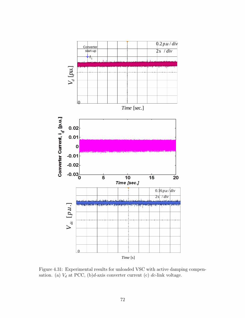
[sec.]Time
[.
.]d
Vpu
0.2 . /
2s /
p u div
divConverter
start-up
0
1t
[s]Time
[.
.]dc
Vp
u
0.16 . /
2s /
p u div
div
0
Figure 4.31: Experimental results for unloaded VSC with active damping compen-sation. (a) Vd at PCC, (b)d-axis converter current (c) dc-link voltage.
72
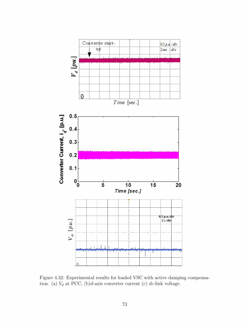
[.
.]dc
Vp
u
0.5 p.u./div
2 s /div
0
Figure 4.32: Experimental results for loaded VSC with active damping compensa-tion. (a) Vd at PCC, (b)d-axis converter current (c) dc-link voltage.
73

4.6 Summary
Several active damping techniques have been proposed in this chapter to reshape
the output impedance of a VSC. Different injection points in: the inner loop,
dc-voltage outer loop, and PLL loop are highlighted and investigated. An experi-
mental validation shows the effectiveness of the active damping impedance based
controller.
74
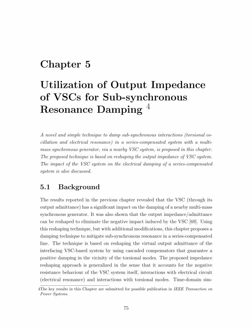
Chapter 5
Utilization of Output Impedanceof VSCs for Sub-synchronousResonance Damping 4
A novel and simple technique to damp sub-synchronous interactions (torsional os-
cillation and electrical resonance) in a series-compensated system with a multi-
mass synchronous generator, via a nearby VSC system, is proposed in this chapter.
The proposed technique is based on reshaping the output impedance of VSC system.
The impact of the VSC system on the electrical damping of a series-compensated
system is also discussed.
5.1 Background
The results reported in the previous chapter revealed that the VSC (through its
output admittance) has a significant impact on the damping of a nearby multi-mass
synchronous generator. It was also shown that the output impedance/admittance
can be reshaped to eliminate the negative impact induced by the VSC [69]. Using
this reshaping technique, but with additional modifications, this chapter proposes a
damping technique to mitigate sub-synchronous resonance in a series-compensated
line. The technique is based on reshaping the virtual output admittance of the
interfacing VSC-based system by using cascaded compensators that guarantee a
positive damping in the vicinity of the torsional modes. The proposed impedance
reshaping approach is generalized in the sense that it accounts for the negative
resistance behaviour of the VSC system itself, interactions with electrical circuit
(electrical resonance) and interactions with torsional modes. Time-domain sim-
4The key results in this Chapter are submitted for possible publication in IEEE Transaction onPower Systems.
75

TZ
Synch. genTr. Inf system
Compensated line
Multi-mass mech. sys
Exe Gen LP HP
VSC
Filter2LX2R
cX 1LX1R
sysXsysR
Figure 5.1: System under study – IEEE SBM with VSC-interfaced system.
ulation results are presented to validate the theoretical analysis and show the
effectiveness of the proposed approach. The IEEE second benchmark (SBM) for
sub-synchronous resonance (SSR) studies is adopted to demonstrate the effective-
ness of the proposed damping technique.
5.2 IEEE SBM Sub-Synchronous Resonance Anal-
yses
In this section, the sub-synchronous interaction analyses are presented for the base
case IEEE SBM system and with added VSC system.
5.2.1 Analysis of IEEE Second Benchmark - Base case
Figure 5.1 shows the system studied in this Chapter which is based on the IEEE
SBM for SSR studies [70] with an added VSC-based system. The synchronous
generator has multi-mass turbines with three torsional modes: Mode#1: 24.65Hz
(0.41 p.u.), Mode#2: 32.39 Hz (0.54 p.u.) and Mode#3: 51.1 Hz (0.852 p.u.).
Torsional resonance interaction appears when the electrical natural frequencies
and mechanical system natural frequencies are complementary. Figure 5.2 shows
the electrical damping profile for the base-case of the IEEE SBM system (without
a VSC) when the compensation level varies from 10-90% (the compensation level
is defined as (X L1/ X C)).The curves are obtained when the synchronous machine
is unloaded and fully loaded. The stars on the plots represent the mechanical
torsional modes of the SBM system. The results reveal that the damping profile
under the loaded condition is highly degraded compared with the no-load case.
This reduction needs to be considered when designing sub-synchronous resonance
damping (SSRD) controllers (considered as the worst case). The further investi-
gations, using the scanning analysis, showed that the maximum negative damping
76
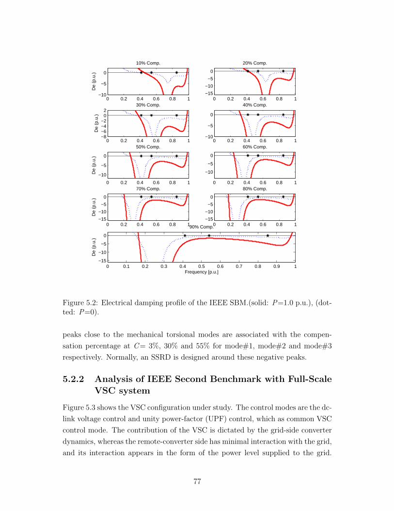
0 0.2 0.4 0.6 0.8 1−10
−5
0
De
(p.u
.)
10% Comp.
0 0.2 0.4 0.6 0.8 1−15
−10
−5
0
20% Comp.
0 0.2 0.4 0.6 0.8 1−8−6−4−2
02
De
(p.u
.)
30% Comp.
0 0.2 0.4 0.6 0.8 1−10
−5
0
40% Comp.
0 0.2 0.4 0.6 0.8 1
−10
−5
0
De
(p.u
.)
50% Comp.
0 0.2 0.4 0.6 0.8 1
−10
−5
0
60% Comp.
0 0.2 0.4 0.6 0.8 1−15
−10
−5
0
De
(p.u
.)
70% Comp.
0 0.2 0.4 0.6 0.8 1−15
−10
−5
0
80% Comp.
0 0.1 0.2 0.3 0.4 0.5 0.6 0.7 0.8 0.9 1−15
−10
−5
0
De
(p.u
.)
Frequency [p.u.]
90% Comp.
Figure 5.2: Electrical damping profile of the IEEE SBM.(solid: P=1.0 p.u.), (dot-ted: P=0).
peaks close to the mechanical torsional modes are associated with the compen-
sation percentage at C = 3%, 30% and 55% for mode#1, mode#2 and mode#3
respectively. Normally, an SSRD is designed around these negative peaks.
5.2.2 Analysis of IEEE Second Benchmark with Full-ScaleVSC system
Figure 5.3 shows the VSC configuration under study. The control modes are the dc-
link voltage control and unity power-factor (UPF) control, which as common VSC
control mode. The contribution of the VSC is dictated by the grid-side converter
dynamics, whereas the remote-converter side has minimal interaction with the grid,
and its interaction appears in the form of the power level supplied to the grid.
77
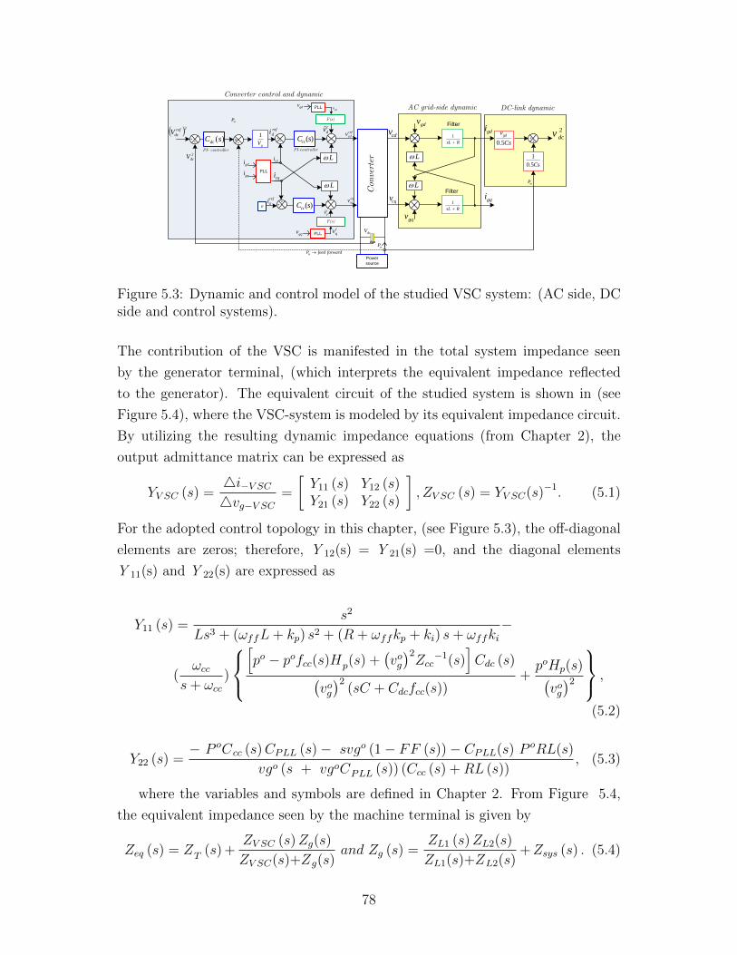
L
L
ref
cdv
ref
cqv cqv
cdv
Con
vert
er
gdv
RsL
1
RsL
1
L
L
gdv
gqv
gdi
gqi
Filter
Filter
+-
+-
Power
source
ref
qi
c
qv
inP
inP feed forward
ref
di
dcV
)(sCcc
)(sCcc
ˆc
dv
PLL AC grid-side dynamic
F(s)
0ˆc
qv
PLL
gdv
gqv
PI-controller
PLL
cqi
cdigd
gq
i
i
2ref
dcV
-+
2
dcV
-1
gV+
PI- controller
inP
2
dcv0.5
gdv
Cs++
1
0.5Cs
inP
Converter control and dynamic
( )dcC s
DC-link dynamic
F(s)
Figure 5.3: Dynamic and control model of the studied VSC system: (AC side, DCside and control systems).
The contribution of the VSC is manifested in the total system impedance seen
by the generator terminal, (which interprets the equivalent impedance reflected
to the generator). The equivalent circuit of the studied system is shown in (see
Figure 5.4), where the VSC-system is modeled by its equivalent impedance circuit.
By utilizing the resulting dynamic impedance equations (from Chapter 2), the
output admittance matrix can be expressed as
YV SC (s) =4i−V SC4vg−V SC
=
[Y11 (s) Y12 (s)Y21 (s) Y22 (s)
], ZV SC (s) = YV SC(s)−1. (5.1)
For the adopted control topology in this chapter, (see Figure 5.3), the off-diagonal
elements are zeros; therefore, Y 12(s) = Y 21(s) =0, and the diagonal elements
Y 11(s) and Y 22(s) are expressed as
Y11 (s) =s2
Ls3 + (ωffL+ kp) s2 + (R + ωffkp + ki) s+ ωffki−
(ωcc
s+ ωcc)
[po − pofcc(s)Hp(s) +
(vog)2Zcc−1(s)
]Cdc (s)(
vog)2
(sC + Cdcfcc(s))+poHp(s)(vog)2
,
(5.2)
Y22 (s) =− P oCcc (s)CPLL (s)− svgo (1− FF (s))− CPLL(s) P oRL(s)
vgo (s + vgoCPLL (s)) (Ccc (s) +RL (s)), (5.3)
where the variables and symbols are defined in Chapter 2. From Figure 5.4,
the equivalent impedance seen by the machine terminal is given by
Zeq (s) = ZT (s) +ZV SC (s)Zg(s)
ZV SC(s)+Zg(s)and Zg (s) =
ZL1 (s)ZL2(s)
ZL1(s)+ZL2(s)+Zsys (s) . (5.4)
78
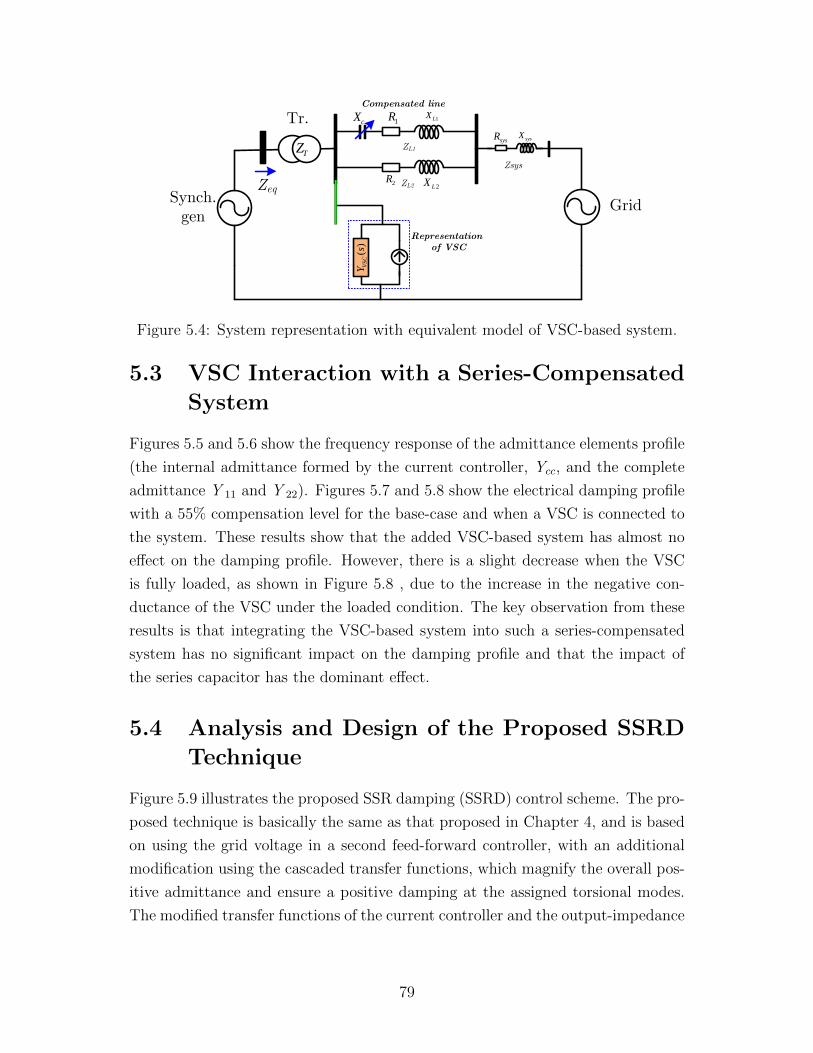
TZ
Synch. gen
Tr.
Grid
Compensated line
2LX2R
cX 1LX1R
sysXsysR
()
VSC
Ys
Representation of VSC
Zeq
Zsys
ZL1
ZL2
Figure 5.4: System representation with equivalent model of VSC-based system.
5.3 VSC Interaction with a Series-Compensated
System
Figures 5.5 and 5.6 show the frequency response of the admittance elements profile
(the internal admittance formed by the current controller, Ycc, and the complete
admittance Y 11 and Y 22). Figures 5.7 and 5.8 show the electrical damping profile
with a 55% compensation level for the base-case and when a VSC is connected to
the system. These results show that the added VSC-based system has almost no
effect on the damping profile. However, there is a slight decrease when the VSC
is fully loaded, as shown in Figure 5.8 , due to the increase in the negative con-
ductance of the VSC under the loaded condition. The key observation from these
results is that integrating the VSC-based system into such a series-compensated
system has no significant impact on the damping profile and that the impact of
the series capacitor has the dominant effect.
5.4 Analysis and Design of the Proposed SSRD
Technique
Figure 5.9 illustrates the proposed SSR damping (SSRD) control scheme. The pro-
posed technique is basically the same as that proposed in Chapter 4, and is based
on using the grid voltage in a second feed-forward controller, with an additional
modification using the cascaded transfer functions, which magnify the overall pos-
itive admittance and ensure a positive damping at the assigned torsional modes.
The modified transfer functions of the current controller and the output-impedance
79
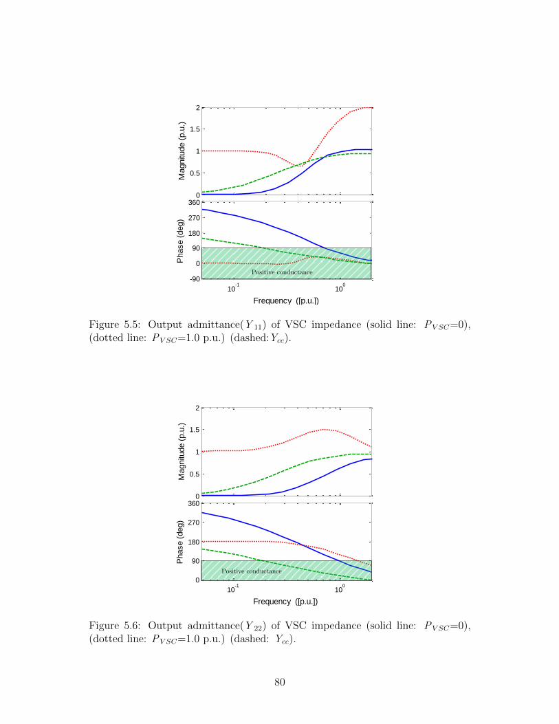
0
0.5
1
1.5
2
Magnitu
de (
p.u
.)
10-1
100
-90
0
90
180
270
360
Phase (
deg)
Frequency ([p.u.])
Positive conductance
Figure 5.5: Output admittance(Y 11) of VSC impedance (solid line: PV SC=0),(dotted line: PV SC=1.0 p.u.) (dashed:Ycc).
0
0.5
1
1.5
2
Magnitu
de (
p.u
.)
10-1
100
0
90
180
270
360
Phase (
deg)
Frequency ([p.u.])
Positive conductance
Figure 5.6: Output admittance(Y 22) of VSC impedance (solid line: PV SC=0),(dotted line: PV SC=1.0 p.u.) (dashed: Ycc).
80

Figure 5.7: Electrical damping with SG loading is P=1.0 p.u.: (Solid: base-case-without VSC), (dotted: with PV SC=1.0 p.u).; (dashed: PV SC= 0) (C =55%).
Figure 5.8: Electrical damping with SG loading is P=0 p.u.: (Solid: base case-without VSC), (dotted: with PV SC=1.0 p.u).; (dashed: PV SC= 0) (C =55%).
with the proposed SSRD controller can be expressed by
i =
{C (s)
L (s) + C (s)
}︸ ︷︷ ︸
fcc
iref +
{[1−H (s) +B (s)C(s)]
[L (s) + C (s)]
}︸ ︷︷ ︸
Y Newcc =1/ZNew
cc
vg (5.5)
where
B (s) = B1 (s) +B2 (s) + · · ·+Bx (s) ,
and
Bx (s) =2ζkcxωcxs
s2 + 2sζωcx + ω2cx
.
The compensator B(s) should be designed to operate only in transient condi-
tions and chosen to maximize the positive admittance that appears in the sub-
synchronous region, particularly in the vicinity of the torsional modes. To meet
these requirements, the compensator, B(s), can be designed as either a band-pass
compensator (BPC) or a high-pass compensator(HPC) or a mixed compensator,
which yields a zero-dc-gain and facilitates the shaping of the output admittance
81
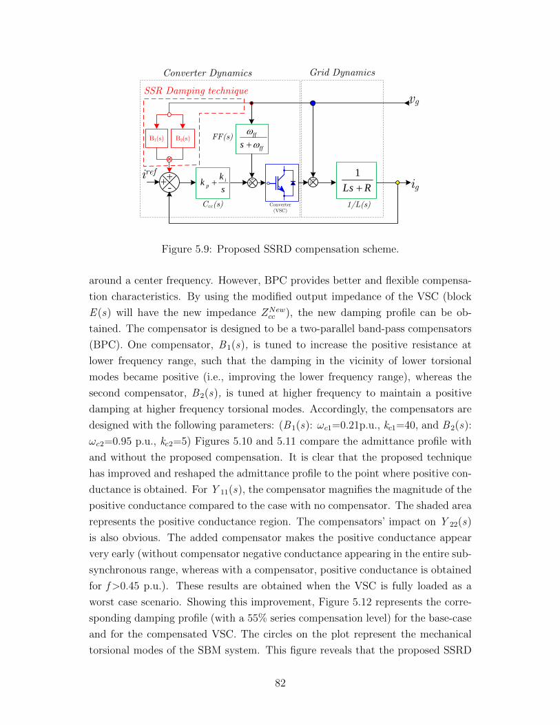
-- ++ i
p
kk
s
ff
ffs
1
Ls R
FF(s)
1/L(s)Ccc(s) Converter(VSC)
Grid Dynamics
ig
vg
iref ++
+
Converter Dynamics
SSR Damping technique
B2(s)B1(s)
++
Figure 5.9: Proposed SSRD compensation scheme.
around a center frequency. However, BPC provides better and flexible compensa-
tion characteristics. By using the modified output impedance of the VSC (block
E (s) will have the new impedance ZNewcc ), the new damping profile can be ob-
tained. The compensator is designed to be a two-parallel band-pass compensators
(BPC). One compensator, B1(s), is tuned to increase the positive resistance at
lower frequency range, such that the damping in the vicinity of lower torsional
modes became positive (i.e., improving the lower frequency range), whereas the
second compensator, B2(s), is tuned at higher frequency to maintain a positive
damping at higher frequency torsional modes. Accordingly, the compensators are
designed with the following parameters: (B1(s): ωc1=0.21p.u., kc1=40, and B2(s):
ωc2=0.95 p.u., kc2=5) Figures 5.10 and 5.11 compare the admittance profile with
and without the proposed compensation. It is clear that the proposed technique
has improved and reshaped the admittance profile to the point where positive con-
ductance is obtained. For Y 11(s), the compensator magnifies the magnitude of the
positive conductance compared to the case with no compensator. The shaded area
represents the positive conductance region. The compensators’ impact on Y 22(s)
is also obvious. The added compensator makes the positive conductance appear
very early (without compensator negative conductance appearing in the entire sub-
synchronous range, whereas with a compensator, positive conductance is obtained
for f>0.45 p.u.). These results are obtained when the VSC is fully loaded as a
worst case scenario. Showing this improvement, Figure 5.12 represents the corre-
sponding damping profile (with a 55% series compensation level) for the base-case
and for the compensated VSC. The circles on the plot represent the mechanical
torsional modes of the SBM system. This figure reveals that the proposed SSRD
82

0
10
20
30
40
50
Magnitu
de (
p.u
.)
10-1
100
-90
-45
0
45
90
Phase (
deg)
Frequency ([p.u.])
Figure 5.10: Output admittance (Y 11) with proposed active damping. (dotted:base case VSC system) (solid: compensated VSC system).
is able to stabilize the torsional modes by creating positive electrical damping at
their frequency modes. (This result is due to the positive conductance added by
the compensator).
The modified SSR compensator was tested under other compensation levels.
Figure 5.13 shows the damping profile with different series compensation levels:
3%, 30% and 90%. The obtained results verify that the proposed approach suc-
cessfully improves the damping profile at the torsional modes.
5.5 Impact of the Proposed Technique on VSC
Dynamics
According to the control system requirements, a modified control system should
not impact the tracking or violate the disturbance rejection capability of the con-
trolled system. Therefore, the impact of the proposed damping controller on the
current-control performance is evaluated to ensure an effective tracking and distur-
bance rejection performance when the compensator is used. Figure 5.14 shows the
current tracking response for a unit-step reference command with and without the
proposed controller. It is clear that the dc-gain of the active compensator is zero,
and the active compensator does not affect the tracking performance (as previously
83

0
5
10
15
Magnitu
de (
p.u
.)
10-1
100
0
45
90
135
180
225
Phase (
deg)
Frequency ([p.u.])
Positive conductance Appearance of
+ve cond.
Figure 5.11: Output admittance (Y 22) with proposed active damping: (dotted:base case VSC system) (solid: compensated VSC system).
0 0.1 0.2 0.3 0.4 0.5 0.6 0.7 0.8 0.9 1−40
−30
−20
−10
0
10
20
De
(p.u
.)
Frequency [p.u.]
Figure 5.12: Electrical damping (C =55%) (dotted: IEEE SBM base case) (solid:IEEE SBM with proposed compensation).
84

0 0.1 0.2 0.3 0.4 0.5 0.6 0.7 0.8 0.9 1−10
−5
0
5
10
De
(p.u
.)
Frequency [p.u.]
(a)
0 0.1 0.2 0.3 0.4 0.5 0.6 0.7 0.8 0.9 1−20
−15
−10
−5
0
5
10
15
20
De
(p.u
.)
Frequency [p.u.]
(b)
0 0.1 0.2 0.3 0.4 0.5 0.6 0.7 0.8 0.9 1−20
−15
−10
−5
0
5
10
15
20
De
(p.u
.)
Frequency [p.u.]
(c)
Figure 5.13: Electrical damping profile. (dotted: IEEE SBM base case) (solid:IEEE SBM with proposed compensation), under series compensation levels (a)C=3%, (b)C =30%, (c)C =90%.
85

1 1.002 1.004 1.006 1.008 1.010
0.2
0.4
0.6
0.8
1
Time [s]
Cur
rent
ste
p re
spon
se
Figure 5.14: Tracking response of closed loop current controller with and withoutcompensation, (dashed: without compensator) (dotted: with compensator).
1 1.05 1.1 1.15 1.2−0.05
0
0.05
0.1
0.15
Time [s]
Rel
ativ
e st
ep r
espo
nse
Figure 5.15: Disturbance rejection (dashed: base case) (dotted: compensated).
proved in (5.5) ). Figure 5.15 presents the impact of the proposed controller on
the disturbance rejection performance. This figure shows the current response due
to (0.1 p.u.) step disturbances in the grid voltage with and without the proposed
active impedance controller. It is observed that the proposed approach does not
violate the disturbance rejection capability of the VSC as the converter rejects the
disturbance quickly (within 50 ms). During grid-voltage transients, the compen-
sator dynamics yield a transient component that is added to the reference current
to shape the converter output admittance; the transient component is directly
reflected to the current response. However, if the compensator parameters are
designed appropriately, the transient component will swiftly vanish without signif-
icant converter overload. It should be noted that the effect of the proposed SSRD
compensator is limited to the current control performance as the compensator does
not influence the outer loops dynamics.
86

2 4 6 8 10 12 14 16 18 20−5
0
5
TH
P−
LP [p
.u.]
2 4 6 8 10 12 14 16 18 20−10
0
10
TLP
−G
EN
[p.u
.]
2 4 6 8 10 12 14 16 18 20−0.1
0
0.1
0.2
Time [s]
TE
XE
−G
EN
[p.u
.]
Figure 5.16: IEEE SBM base-case time-domain simulation. (without VSC sys-tem).
5.6 Time-Domain Simulation Results
A detailed time-domain model of the studied system is implemented in PSCAD/EMTDCr
package to verify the theoretical damping analysis. A transient disturbance (a
three-phase fault) occurred at t=2.0 s. Figure 5.16 shows the torque responses
for the base-case with a 55% compensation level. This compensation level inter-
acts with the torsional mode#1 and creates an unstable condition. The series-
compensated line induces negative damping that destabilizes the torsional mode
(the oscillatory response is building up). Figure 5.17 shows the torque responses
when the proposed SSRD is implemented, revealing that the proposed active damp-
ing controller successfully injects positive damping in the torsional mode, and yields
damped responses. The time-domain results are in agreement with the analytical
analysis. Figures 5.18, 5.19, and 5.20 show the VSC PCC voltage, dc-link volt-
age, and output power, respectively, revealing that the additional transients in the
converter variables are within the converter capability and vanish quickly.
5.7 Summery
A new technique to damp SSR in a series-compensated line system based on re-
shaping the output admittance of the grid-side converter of a nearby VSC-based
system has been proposed in this chapter. The robustness of the proposed SSRD
controller has been verified under different series compensation levels. The impact
87

2 4 6 8 10 12 14 16 18 20−0.5
0
0.5
TH
P−
LP [p
.u.]
2 4 6 8 10 12 14 16 18 20−1
0
1
2T
LP−
GE
N [p
.u.]
2 4 6 8 10 12 14 16 18 20−0.1
0
0.1
0.2
Time [s]
TE
XE
−G
EN
[p.u
.]
Figure 5.17: IEEE SBM Time-domain simulation with the proposed SSRD tech-nique.
2.9 3 3.1 3.2 3.3 3.4
−1
−0.8
−0.6
−0.4
−0.2
0
0.2
0.4
0.6
0.8
1
PC
C V
olta
ge [p
.u.]
Time [s]
Figure 5.18: Output voltage of VSC at the point of common coupling.
88
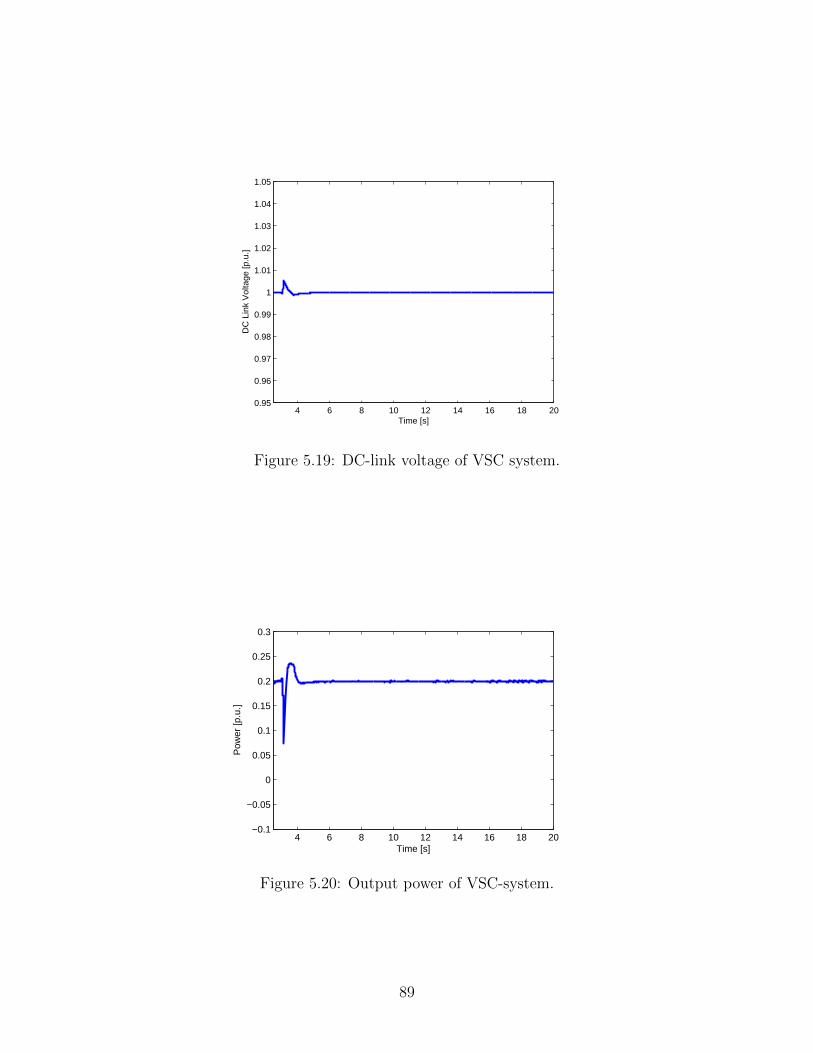
4 6 8 10 12 14 16 18 200.95
0.96
0.97
0.98
0.99
1
1.01
1.02
1.03
1.04
1.05
DC
Lin
k V
olta
ge [p
.u.]
Time [s]
Figure 5.19: DC-link voltage of VSC system.
4 6 8 10 12 14 16 18 20−0.1
−0.05
0
0.05
0.1
0.15
0.2
0.25
0.3
Pow
er [p
.u.]
Time [s]
Figure 5.20: Output power of VSC-system.
89

of the added compensator on the converter performance is also discussed. The
effectiveness of the active compensation is proved by theoretical analysis and time-
domain simulation results by using the IEEE SBM. It should be noted that the
proposed SSRD is within the inner loop dynamics and does not impact other loops
dynamic. The impact of integrating a VSC-based system into such a system has
been also investigated and pointed out in this chapter. It has been found that the
VSC with dc-link voltage control and unity power-factor control had no significant
impact on the electrical damping of a series-compensated line, and the impact of
the series capacitor is the dominant.
90

Chapter 6
VSC Output Impedance underPower Synchronization Control 5
In the previous chapters, the output impedance of a VSC system is developed and
analyzed under the standard vector current control (VCC) strategy. In this chapter,
the analysis of the output impedance of a VSC system under power synchronization
control (PSC) topology is presented. The impact of the passivity of the impedance
on the sub-synchronous damping profile of electrically-nearby synchronous genera-
tors is then characterized. The impact of the control modes and control parameter
is identified and addressed. The results reveal that under this control strategy, the
VSC does not exhibit negative damping; in contrast, it has a positive impact, com-
pared to that of the commonly used vector current control, which has the potential
to degrade the system damping. Time-domain simulation results are presented to
validate the key results obtained from the theoretical analyses.
6.1 Background
The vector current control is the state-of-the-art controller of the power electronics
and voltage-sourced converter systems due to its merits over the conventional di-
rect power control [39]. Under the vector current control strategy, as demonstrated
in this thesis, a VSC-based system can degrade the overall system damping, due to
manifestation of the negative resistance in the sub-synchronous frequency ranges.
Among the control loops, the phase-locked loop (PLL) makes a significant contri-
bution to the negative damping. Even though the vector control is a dominant
control system, it has further limitations when the VSC is connected to a weak
grid [39]-[41]. The main factor is the unstable operation of the PLL in a weak grid.
5This work is submitted for possible publication in IEEE Transaction on Power Systems.
91
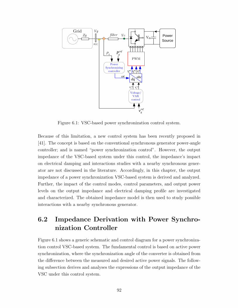
Grid Zg
Vdc
PCC
VgVc
t
ref
gv
ref
dV ref
qV
ref ref ref
a b cV V V
Power Synchronizing
controller
Voltage/VAR
control
Pg
abcdq
ref
gP
Power
Source
filter
PWM
Figure 6.1: VSC-based power synchronization control system.
Because of this limitation, a new control system has been recently proposed in
[41]. The concept is based on the conventional synchronous generator power-angle
controller; and is named “power synchronization control”. However, the output
impedance of the VSC-based system under this control, the impedance’s impact
on electrical damping and interactions studies with a nearby synchronous gener-
ator are not discussed in the literature. Accordingly, in this chapter, the output
impedance of a power synchronization VSC-based system is derived and analyzed.
Further, the impact of the control modes, control parameters, and output power
levels on the output impedance and electrical damping profile are investigated
and characterized. The obtained impedance model is then used to study possible
interactions with a nearby synchronous generator.
6.2 Impedance Derivation with Power Synchro-
nization Controller
Figure 6.1 shows a generic schematic and control diagram for a power synchroniza-
tion control VSC-based system. The fundamental control is based on active power
synchronization, where the synchronization angle of the converter is obtained from
the difference between the measured and desired active power signals. The follow-
ing subsection derives and analyses the expressions of the output impedance of the
VSC under this control system.
92

6.2.1 Grid Dynamic Model
The grid dynamic equations in a dq-rotating reference-frame are given as
vcd = vgd + Ldiddt
+Rid − ωsLiq, (6.1)
vcq = vgq + Ldiqdt
+Riq + ωsLid, (6.2)
where vcd, vcq, vgd, vgq are the direct and quadrature voltage components at the
converter terminal and the grid terminal (at the point of common coupling (PCC)),
respectively; id and iq are the direct and quadrature current components; R and
L are the resistance and inductance of the filter and step-up transformer; and ωs
is the grid angular frequency. The converter terminal voltage can be expressed in
exponential form by
vc = Vcejθc = Vccos (θc)︸ ︷︷ ︸
vcd
+j Vcsin (θc)︸ ︷︷ ︸vcq
, (6.3)
where Vc and θc are the converter voltage magnitude and load angle. By using
(6.3), (6.1) and (6.2)) can be rewritten as
Ldiddt
= Vccos (θc) − vgd −Rid + ωsLiq, (6.4)
Ldiqdt
= Vcsin (θc) − vgq −Riq − ωsLid. (6.5)
In the power synchronization control scheme, Vc and θc are the control variables
regulated by the controller to achieve the desired reference signals, (i.e., the mag-
nitude of the ac-voltage at PCC and the active power).
6.2.2 Control Dynamic Model
The power synchronization control, as a new control method for VSC-based sys-
tems, is different from the conventional vector-current control, in its basic operation
. The control system consists of two inner loops. The first one is the active power
synchronization controller loop, which is the heart of the control system (similar
to the inner current controller loop for vector-current control), and actually serves
two purposes: in addition to performing the synchronization task (which is done by
the PLL in vector-current control), it also controls the active power. The second
loop is the ac-voltage controller loop, which controls the ac-voltage at the PCC. In
some applications, other (outer) loops might be used, such as the dc-link voltage
controller and reactive power loops. The arrangements of these controllers depend
on the application of the VSC.
93

2ref
dcV
-+
2
dcV
+-
gP
refP c ++
gt
t
dcC
PSLC
Constant refP
refP
Synchronizing controller DC controller
Figure 6.2: DC-link voltage and power synchronioztion controls.
VdcPgPinPout
Grid
Figure 6.3: Energy balance on the dc-link.
6.2.3 Power Synchroniounztion and DC Voltage Loops
Figure 6.2 depicts the active power control block diagram. This loop is based on
the power difference between the measured active power and the required active
power set value. The difference is then processed by a controller (C PSL); the output
of the controller is the angle (θc) used to regulate the converter power (changing
the angle, which fundamentally changes the modulation pattern to regulate the
converter output active power). Then the angle is added to the grid frequency
to provide synchronization signal to the converter. The power synchronization is
decribed by
θc = CPSL(P ref − Pg
)(6.6)
and
ωt = ωgt+ θc. (6.7)
The linearization of (6.6) gives the change in the load angle needed to obtain the
required active power as
∆θc = −CPSL∆Pg. (6.8)
The grid power equation in the dq-frame and its small-signal version are given as
Pg = vgdigd + vgqigq, (6.9)
∆P g = ∆vgdiod + ∆idv
og + ∆vgqi
oq + ∆vgqi
oq. (6.10)
The input power reference signal to the power synchronization loop can be obtained
either directly from a constant reference power or through the dc-link voltage
controller, as illustrated in Figure 6.2. In the case of direct power control, only one
94
inner loop is used in the VSC control system: the power synchroniztion loop to
regulate the power. This configuration exists, for example, at the rectifier station of
a HVDC system, whereas other inverter station has a dc-link voltage controller, and
at the generator-side converter in wind turbines application. For a dc-link voltage
controller, the reference power signal is obtained through the energy balance over
the dc-link. The energy in the capacitor is the difference between the input and
the output power to/from the dc-link terminals as depicted in Figure 6.3. With a
lossless converter (i.e., Pg=Pout), the energy in the capacitor can be described by
0.5Cdv2
cd
dt= Pin − P g. (6.11)
where Pg is the grid-side power, and Pout is the input (source)-side power.
Equation (6.11) shows that the dc-link voltage can be used to control the grid
power, therefore, the reference power signal is obtained as follows:
P ref =Cdc(s)
2
(⟨vrefdc
⟩2
− v2dc
), (6.12)
where Cdc(s) is the dc-link voltage PI-controller.
With vrefdc = vodc, the linearized equations of the active power loop are obtained
as
∆P ref = −Cdcvodc∆vdc. (6.13)
Substituting (6.13) in (6.6) yields
∆θc = CPSL (−Cdcvodc∆vdc −∆Pg) . (6.14)
With Pin = P o, the small-signal of (6.11) is
sCvdco∆vdc ≈ −∆Pg. (6.15)
6.2.4 Voltage/VAr Control Loops
The block diagram of the ac-voltage control is shown in Figure 6.4(a). Basically,
the controller regulates the magnitude of the converter terminal voltage in order
to maintain the PCC voltage at a desired set point. The voltage control law is
described by
Vc = ∆V + vog , (6.16)
where Vc is the converter terminal voltage; ∆V represents the additional voltage
difference; vog is the initial PCC grid voltage , which is typically set to 1.0 p.u. ;
and ∆V is obtained from the voltage control law
∆V = Cv(s)(vrefg − |vg|
), (6.17)
95
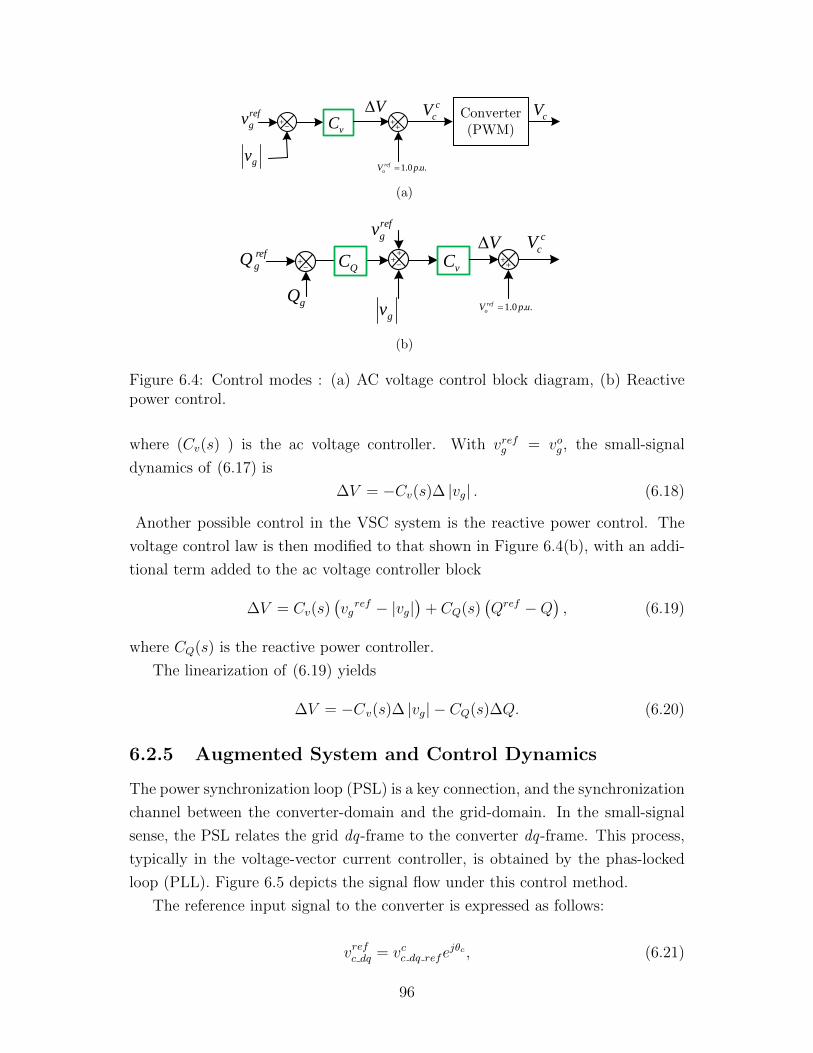
c
cVref
gv +vC
gv
-
V++
1.0 . .ref
oV p u
Converter (PWM)
cV
(a)
ref
gQ +- QC
gQ
++
vC +
gv
-
ref
gv
1.0 . .ref
oV p u
+
c
cVV
(b)
Figure 6.4: Control modes : (a) AC voltage control block diagram, (b) Reactivepower control.
where (Cv(s) ) is the ac voltage controller. With vrefg = vog , the small-signal
dynamics of (6.17) is
∆V = −Cv(s)∆ |vg| . (6.18)
Another possible control in the VSC system is the reactive power control. The
voltage control law is then modified to that shown in Figure 6.4(b), with an addi-
tional term added to the ac voltage controller block
∆V = Cv(s)(vgref − |vg|
)+ CQ(s)
(Qref −Q
), (6.19)
where CQ(s) is the reactive power controller.
The linearization of (6.19) yields
∆V = −Cv(s)∆ |vg| − CQ(s)∆Q. (6.20)
6.2.5 Augmented System and Control Dynamics
The power synchronization loop (PSL) is a key connection, and the synchronization
channel between the converter-domain and the grid-domain. In the small-signal
sense, the PSL relates the grid dq-frame to the converter dq-frame. This process,
typically in the voltage-vector current controller, is obtained by the phas-locked
loop (PLL). Figure 6.5 depicts the signal flow under this control method.
The reference input signal to the converter is expressed as follows:
vrefc dq = vcc dq refejθc , (6.21)
96

c
cdq_
_
c
cd ref
c
cq ref
V
V
r e f
r e f
Q
V
AC Voltage/VAR controller
gdq
ref
cd
ref
cq
V
V Converter(&PWM)
cd
cq
V
V
DC /Power Controller
Synchronization
controller
ref
dc
ref
v
P
Figure 6.5: Signal flow of the power synchronization control system in the dq-references frame.
where the superscript “c” donates the converter frame. In modern high-power
VSCs, the operation of the PWM is in the range of a few kHz. With such switching
frequencies, the output converter current can quickly track its reference, and the
output signal of the converter is equal to its input reference as described by
Vc dq = vrefc dq = vcc dq refejθc . (6.22)
If the active power and the ac voltage loops are only considered, substitute (6.16)
in (6.22) yields
Vcd = vcdref cos (θc) = (∆V + vog)cos (θc)
Vcq = vcqref sin (θc) = (∆V + vog)sin (θc)
}. (6.23)
Now, by substituting (6.23) in the grid dynamic equations (6.4 and 6.5) and lin-
earizing the equations around a stable operation point, yields
Ld∆iddt
= ∆V cos (θco) − vog∆θcsin (θco) −∆vgd −R∆id + ωoL∆iqLd∆iq
dt= ∆V sin (θco) + vog∆θc cos (θco) −∆vgq −R∆iq − ωoL∆id
}. (6.24)
∆V and ∆θc are the control variables regulated by the control system to achieve the
desired reference signal, i.e., the output of the control dynamics . By substituting
the obtained expression of ∆V and ∆θc from the control equations (6.8) and (6.18)
in (6.24), taking the Laplace transformation, and rearranging the equation, yields
∆id (sL+R)− ωoL∆iq = −Cv∆ |vg| cos (θco) − vog [−CPSL∆Pg] sin (θco) −∆vgd∆iq (sL+R) + ωoL∆id = −Cv∆ |vg| sin (θco) + vog [−CPSL∆Pg] cos (θco) −∆vgd
}.
(6.25)
In the steady-state condition, the q-component of the grid bus is equal the zero,
and the d -component is equal to the voltage magnitude, so ∆ |vg| ≈ ∆vgd; then,
by substituting the small- signal equation of the active power, ∆Pg in (6.10), the
following expressions are obtained:
A1∆vgd = A2∆vgq+A3∆id + A4∆iqB1∆vgq = B2∆vgd +B3∆id +B4∆iq
}, (6.26)
97

where
A1 = [−Cvcos (θco) +CPSLvogiod sin (θco)− 1]
A2 = [−CPSLvogioqsin (θco)]
A3 = [sL+R− CPSLvogvogdsin (θco)]
A4 = [−ωoL− CPSLvogvogq sin (θco)]
B1 = [−CPSLvogioqcos (θco)− 1]
B2 = [[Cvsin (θco) + cos (θco) CPSLv
ogiod
]B3 = [ωoL+ CPSLv
ogdv
og cos (θco)]
B4 = [sL+R + CPSLvogvogq cos (θco)] .
The resulting equations above are interesting because they have only the grid
voltages and grid current as variables. By eliminating the coupling term associated
with the voltages, the impedance can be formed and expressed as follows:[∆vgd(s)∆vgq(s)
]=
[Z11(s) Z12(s)Z21(s) Z22(s)
] [∆id(s)∆iq(s)
], (6.27)
where the impedance elements are given as follows :
Z11 (s) =(A3 + A2
B3
B1)
(A1 − A2B2
B1),
Z12 (s) =(A4 + A2
B4
B1)
(A1 − A2B2
B1),
Z21 (s) =(B3 +B2
A3
A1)
(B1 −B2A2
A1),
Z22 (s) =(B3 +B2
A4
A1)
(B1 −B2A2
A1).
The impedance analysis and control design are presented in the following sections.
6.3 Control Loops and Control Design
This section discusses the control loop configurations and closed loop system design
for PSL.
98

+-
gP
refP( )PSLC s
( )PSLG s gP
Figure 6.6: Power synchronization closed-loop system.
6.3.1 Power Synchronization Contol Design
Figure 6.6 shows the closed-loop power synchronization block diagram, where
GPSL(s) represents the system transfer function between the converter angle, and
the output power and C PSL(s) is the controller. The derivation of the transfer
function GPSL(s) can be obtained as follows [41]. The grid equations in (6.1) can
be linearized as
Ld∆iddt
= −Vo sin (θco) ∆θc −R∆id + ωoL∆iqLd∆iq
dt= −Vo cos (θco) ∆θc −R∆iq − ωoL∆id.
}. (6.28)
From (6.28) , the transfer functions between the grid currents and the converter
voltage angle are
∆id = ωoLvo cos(θco)−(sL+R)vo sin(θco)
(sL+R)2+(ωoL)2∆θc
∆iq = ωoLvo sin(θco)+(sL+R)vo cos(θco)
(sL+R)2+(ωoL)2∆θc.
}. (6.29)
The variation in the grid voltage as a function of the grid current can be also
obtained as∆vgd = sL∆id − ωoLωo∆iq∆vgq = sL∆iq − ωoLωo∆id
}. (6.30)
By substituting the resulting equations of the small-signal currents and voltages
into the power equation, a transfer function that relates the change in the power
due to the change in the converter angle is obtained as
∆P g = GPSL(s)∆θc and GPSL(s) =c1s
2 + c2s+ c3
s2L2 + 2sRL+R2 + (ωoL)2 , (6.31)
where
c1 =L
ωo(vogv
occos (θco) − voc
2)
c2 =R
ωo(vogv
occos (θco) − voc
2)
c3 = ωoLvogv
occos (θco) −Rvogvocsin (θco) .
99
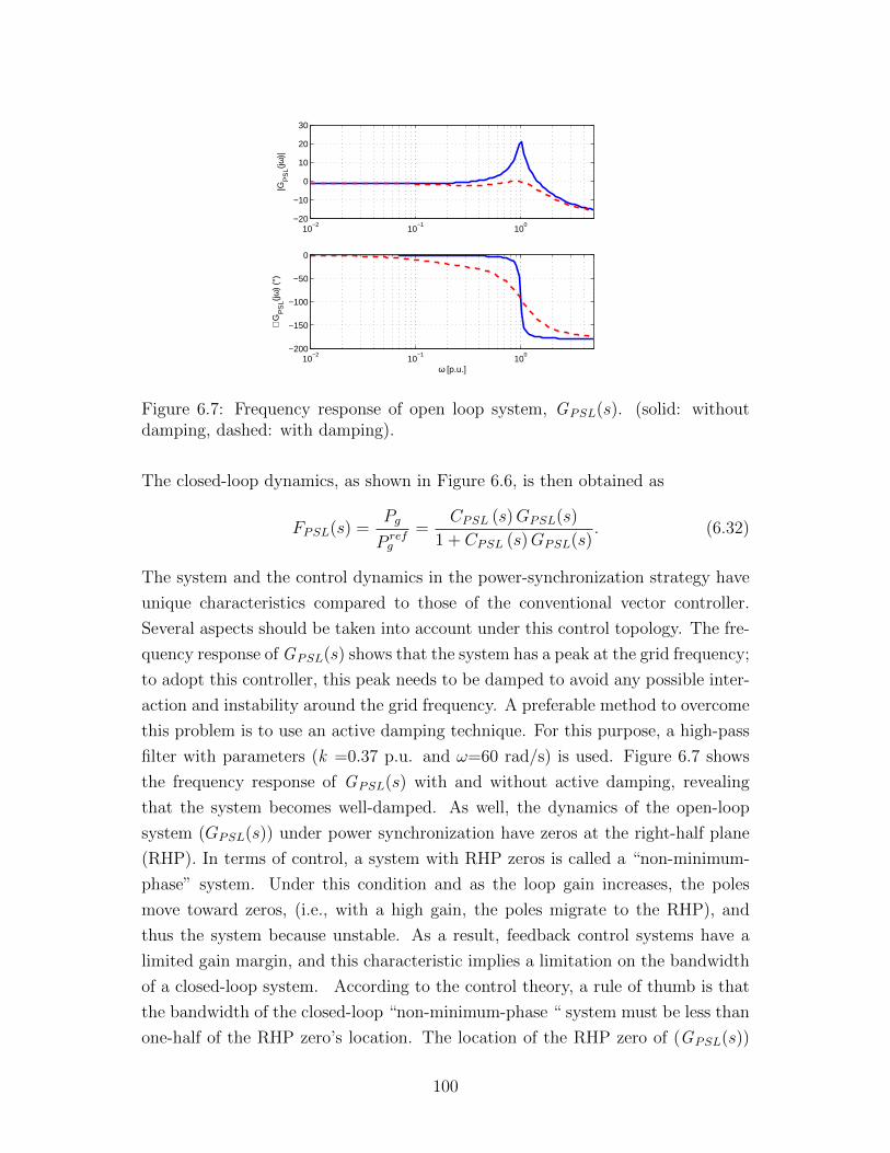
10−2
10−1
100
−20
−10
0
10
20
30
|GP
SL(jω
)|
10−2
10−1
100
−200
−150
−100
−50
0
ω [p.u.]
∠G
PS
L(jω)
(°)
Figure 6.7: Frequency response of open loop system, GPSL(s). (solid: withoutdamping, dashed: with damping).
The closed-loop dynamics, as shown in Figure 6.6, is then obtained as
FPSL(s) =Pg
P refg
=CPSL (s)GPSL(s)
1 + CPSL (s)GPSL(s). (6.32)
The system and the control dynamics in the power-synchronization strategy have
unique characteristics compared to those of the conventional vector controller.
Several aspects should be taken into account under this control topology. The fre-
quency response of GPSL(s) shows that the system has a peak at the grid frequency;
to adopt this controller, this peak needs to be damped to avoid any possible inter-
action and instability around the grid frequency. A preferable method to overcome
this problem is to use an active damping technique. For this purpose, a high-pass
filter with parameters (k =0.37 p.u. and ω=60 rad/s) is used. Figure 6.7 shows
the frequency response of GPSL(s) with and without active damping, revealing
that the system becomes well-damped. As well, the dynamics of the open-loop
system (GPSL(s)) under power synchronization have zeros at the right-half plane
(RHP). In terms of control, a system with RHP zeros is called a “non-minimum-
phase” system. Under this condition and as the loop gain increases, the poles
move toward zeros, (i.e., with a high gain, the poles migrate to the RHP), and
thus the system because unstable. As a result, feedback control systems have a
limited gain margin, and this characteristic implies a limitation on the bandwidth
of a closed-loop system. According to the control theory, a rule of thumb is that
the bandwidth of the closed-loop “non-minimum-phase “ system must be less than
one-half of the RHP zero’s location. The location of the RHP zero of (GPSL(s))
100

10−2
10−1
100
−60
−40
−20
0
20
|FP
SL(jω
)|
10−2
10−1
100
−300
−200
−100
0
100
ω [p.u.]
∠F
PS
L(jω)
(°)
Figure 6.8: Frequency response of closed loop system, FPSL(s). (solid: withoutdamping, dashed: with damping).
Power Synchro. Inner loop
refP
2
dcV
DCP
++
1
0.5Cs
1
0.5Cs
2ref
dcV( )dcC s-
+
2
dcV
P
Figure 6.9: DC-link voltage closed-loop control system.
can be determined by [41]
Z1,2 ≈ ±ωo√
cos θc1− cos θc
. (6.33)
Equation (6.33) reveals that the location of the zeros highly depends on the con-
verter voltage angle. For a light load, the zeros move far away towards the right,
allowing a higher bandwidth, however, for a heavy load, which is actually the lim-
itation of the system, the location of the zeros approaches the fundamental grid
frequency (Z1,2 ≈ ±ωo). These results limits the system bandwidth to be less than
half of the grid angular frequency ( i.e., 188 rad/sec). By considering this limita-
tion in control design, Figure 6.8 shows the frequency response of the closed-loop
system under an integral controller (with gain a ki=90 rad/s, which yields 100
rad/s closed-loop bandwidth).
101

ref
gv + ( )vC s
gv
-
o
V
V
( )VF sgv
Figure 6.10: Block diagram of the ac voltage control dynamics.
6.3.2 DC Control Loop Design
The closed-loop dynamics of the dc-link voltage control system is depicted in Fig-
ure 6.9. The PI-controller is chosen to regulate the dc-link voltage. As an outer
loop, the dynamics of the inner closed loop system (FPSL(s)) is much faster than
those of the outer dc-link voltage control loop, so it is reasonable to assume that
FPSL is unity within the bandwidth of the outer loop. Then, the closed-loop
transfer function of the dc-link voltage control loop can be simplified by
Gdc(s) =
(vrefdc
)2
(vdc)2 =
skpdc + kidc0.5s2C + skpdc + kidc
. (6.34)
Compared to the common second-order transfer function, the control gain can be
designed as ω2n = Kidc
0.5Cand 2ζωn = Kpdc
0.5C. To facilitate a reliable and robust cas-
caded control operation, the bandwidth of the dc-link voltage controller loop is cho-
sen to be four times slower than that of the inner loop (i.e., BWDC = BW PSL/4 ).
With ωn = 25 rad/s, and with ζ = 1, the gains are obtained as kpdc = 0.02 p.u
and kidc = 0.007 p.u.
6.3.3 AC Voltage Control Loop
In the ac voltage control loop, the magnitude of the converter terminal voltage is
regulated to maintain the PCC voltage at a certain value. The transfer function
between the converter voltage and PCC voltage is obtained as [71]
FV (s) =LLgV
oc s
2 +RLgVoc s+ ω2
oLLg
s2L2 + 2sRL+R2 + (ωoL)2 . (6.35)
Figure 6.10 shows a block diagram of the closed loop system, where the closed
loop system is given by
GV (s) =vg
vrefg
=Cv (s)FV (s)
1 + Cv (s)FV (s). (6.36)
102
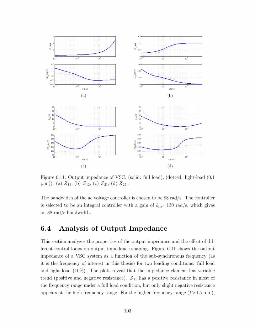
10−2
10−1
100
0
2
4
6
|Z11
(jω)|
10−2
10−1
100
−150
−100
−50
0
50
100
ω [p.u.]
∠Z
11(jω
) (°
)
(a)
10−2
10−1
100
0
0.5
1
1.5
|Z12
(jω)|
10−2
10−1
100
0
50
100
150
ω [p.u.]
∠Z
12(jω
) (°
)
(b)
10−2
10−1
100
0
5
10
15
20
25
|Z21
(jω)|
10−2
10−1
100
80
100
120
140
160
180
ω [p.u.]
∠Z
21(jω
) (°
)
(c)
10−2
10−1
100
0
5
10
15
20
25
|Z22
(jω)|
10−2
10−1
100
50
100
150
200
250
300
ω [p.u.]
∠Z
22(jω
) (°
)
(d)
Figure 6.11: Output impedance of VSC: (solid: full load), (dotted: light-load (0.1p.u.)). (a) Z 11, (b) Z 12, (c) Z 21, (d) Z 22 .
The bandwidth of the ac voltage controller is chosen to be 88 rad/s. The controller
is selected to be an integral controller with a gain of ki v=130 rad/s, which gives
an 88 rad/s bandwidth.
6.4 Analysis of Output Impedance
This section analyzes the properties of the output impedance and the effect of dif-
ferent control loops on output impedance shaping. Figure 6.11 shows the output
impedance of a VSC system as a function of the sub-synchronous frequency (as
it is the frequency of interest in this thesis) for two loading conditions: full load
and light load (10%). The plots reveal that the impedance element has variable
trend (positive and negative resistance). Z 11 has a positive resistance in most of
the frequency range under a full load condition, but only slight negative resistance
appears at the high frequency range. For the higher frequency range (f>0.5 p.u.),
103

Grid
Vdc
Vg
L, R
GSC
i Power
Source
Vcfilter
Pg Qg
Zg
Synch. genTr.
Multi-mass mech. sys
Exe Gen HPLPA LPB IP
TZ
Figure 6.12: System under the study –VSC system connected to the IEEE-FBM.
both impedance profiles merge, and the impact of the loading condition vanishes.
Similarly, Z 12 shows a positive resistance in the entire frequency range, and the
value of the resistance slightly increase with the loading condition. However, the
impact of the loading condition disappears for frequencies higher range. In con-
trast, Z 21 shows an opposite profile. Negative resistance appears across the entire
frequency range with almost constant values. A light load gives less negative re-
sistance. A negative resistance in Z 22 occurs in the entire sub synchronous range,
while slight positive resistance at the lower frequency range.However, like the load-
ing impact for the other impedance elements, the impact of loading fades for higher
frequencies. It is now understood that the impact of the loading condition appears
mainly at the lower frequency range. However, it is also observed that at a higher
frequency range (f>0.5 p.u.) impedance elements reach values equal and opposite
to those of the other impedance elements. This result indicates that the positive
resistance is reduced at higher frequencies, but the overall impedance seems to
have non-negative resistance .
6.5 VSC Dynamics and Grid Interaction
To study the interaction of a VSC with a nearby SG under the power synchroniza-
tion control topology, the IEEE first benchmark (FBM), with a zero compensation
level, is adopted. The schematic diagram of the studied system is shown in Fig-
ure 6.12.
6.5.1 Impedance and System Damping Analysis
Figure 6.13 compares the electrical damping for the base-case (without VSC) and
with a VSC connected under three loading conditions, namely: light-load, half-
104

0 0.1 0.2 0.3 0.4 0.5 0.6 0.7 0.8 0.9 1−1
−0.8
−0.6
−0.4
−0.2
0
0.2
0.4
0.6
0.8
1
De
(p.u
.)
Frequency [p.u.]
Figure 6.13: Electrical damping.(solid: base-case, dotted: with loaded (90%) VSC,dashed -dotted: half loaded VSC) (dashed: with lightly (10%) loaded VSC) withPSG=0.1 p.u.
load, and full-loaded. The corresponding real part of the output impedance of
VSC are depicted in Figure 6.14. This figure reveals that the impact of VSC
highly depends on the operation power (i.e., active power level). Under light
load operation VSC improves the system damping in the entire sub-synchronous
range. As the loading level increases, VSC negatively impact the damping at
very high frequency range, for half-load condition the negative impact occur only
after frequency ( f>0.9 p.u.), and under full-load operating condition, the negative
impact become more obvious and appears at frequency (f>0.78 p.u.). The real-
part of the impedance elements reveals that the VSC exhibit less negative resistance
with light-load (see R21andR22profile) this realization explains the improvement in
the damping profile impedance at low-and med-frequency range. The less impact
at a higher frequency is attributed to the lower bandwidth of the PSL.
The power synchronization loop, from the VSC side regulates the active power
based on the angle (the injection power corresponds to the change in angle); and
from the power system perspective, this process adds some sort of damping (i.e.,
similar to adding mechanical damping to the system as the grid views the power-
synchronization controlled-VSC as a virtual synchronous machine with controlled
damping characteristics).
6.5.2 Sensitivity Studies
The impact of the control modes and control system bandwidths on the output
impedance are investigated and characterized in the subsection.
A) Impact of Power Synchronization Control System Bandwidth
105
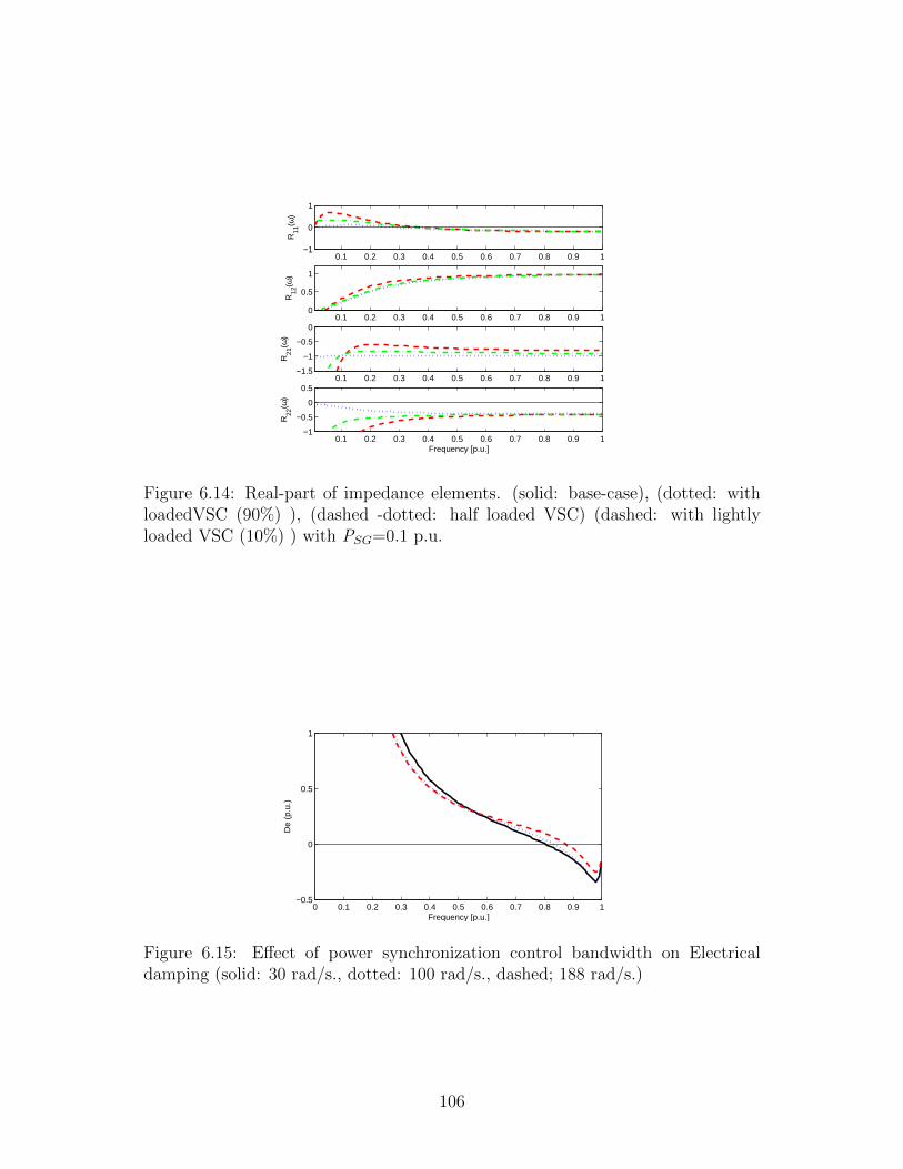
0.1 0.2 0.3 0.4 0.5 0.6 0.7 0.8 0.9 1−1
0
1
R11
(ω)
0.1 0.2 0.3 0.4 0.5 0.6 0.7 0.8 0.9 10
0.5
1
R12
(ω)
0.1 0.2 0.3 0.4 0.5 0.6 0.7 0.8 0.9 1−1.5
−1
−0.5
0
R21
(ω)
0.1 0.2 0.3 0.4 0.5 0.6 0.7 0.8 0.9 1−1
−0.5
0
0.5
R22
(ω)
Frequency [p.u.]
Figure 6.14: Real-part of impedance elements. (solid: base-case), (dotted: withloadedVSC (90%) ), (dashed -dotted: half loaded VSC) (dashed: with lightlyloaded VSC (10%) ) with PSG=0.1 p.u.
0 0.1 0.2 0.3 0.4 0.5 0.6 0.7 0.8 0.9 1−0.5
0
0.5
1
De
(p.u
.)
Frequency [p.u.]
Figure 6.15: Effect of power synchronization control bandwidth on Electricaldamping (solid: 30 rad/s., dotted: 100 rad/s., dashed; 188 rad/s.)
106

0.1 0.2 0.3 0.4 0.5 0.6 0.7 0.8 0.9 1−1
0
1
R11
(ω)
0.1 0.2 0.3 0.4 0.5 0.6 0.7 0.8 0.9 10
0.5
1
R12
(ω)
0.1 0.2 0.3 0.4 0.5 0.6 0.7 0.8 0.9 1−1.5
−1
−0.5
0
R21
(ω)
0.1 0.2 0.3 0.4 0.5 0.6 0.7 0.8 0.9 1−2
−1
0
R22
(ω)
Frequency [p.u.]
Figure 6.16: Effect of power synchronization control bandwidth on real-part ofimpedances; (solid: 30 rad/s., dotted: 100 rad/s., dashed; 188 rad/s.)
Figure 6.15 shows the impact of the bandwidth of the power synchronization
loop on the damping profile and corresponding real-parts are shown in Figure 6.16.
The plots reveal that increase the bandwidth has two opposite impact on the
resistance. The results reveal that the damping improves with inreases in the
bandwidth at higher frequncy range (f>0.5 p.u.), and slight decreases at lower
frequncy range (f<0.5 p.u.). The source of the degrading at low frequnay range
is attributed to the increase in netgaive resisatnce appearence especially ( in R22
element) .The slight improvemnt in the damping at higher frequncy range due
to added extra postive resistance especially at (R21 element). This results is in
agreement with the real-part profile. As the bandwidth increases, the impact of
the PSL is prolonged, and more improvemnt is obtained in the impedance and
damping profiles. Same tends is observed either when VSC is lightly load or full
loaded.
B) Impact of AC Voltage Bandwidth
Figure 6.17demonstrates the impact of the ac voltage bandwidth on the electrical
damping. This figure reveals that increasing the bandwidth has a positive impact
on the damping profile. The impact of the ac voltage loop magnifies at a low
frequency range. As it is observed with higher bandwidth a positive damping is
obtained in the majority of the sub-synchronous range.
C) Effect of Operational Control Mode
107
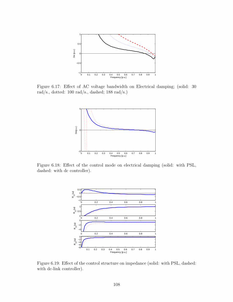
0 0.1 0.2 0.3 0.4 0.5 0.6 0.7 0.8 0.9 1−1
−0.5
0
0.5
1
De
(p.u
.)
Frequency [p.u.]
Figure 6.17: Effect of AC voltage bandwidth on Electrical damping; (solid: 30rad/s., dotted: 100 rad/s., dashed; 188 rad/s.)
0 0.1 0.2 0.3 0.4 0.5 0.6 0.7 0.8 0.9 1−5
0
5
De(
p.u.
)
Frequency [p.u.]
Figure 6.18: Effect of the control mode on electrical damping (solid: with PSL,dashed: with dc controller).
0 0.2 0.4 0.6 0.8 1−1
−0.5
0
0.5
R11
(ω)
0 0.2 0.4 0.6 0.8 10
0.5
1
R12
(ω)
0 0.2 0.4 0.6 0.8 1
−4
−2
0
R21
(ω)
0.1 0.2 0.3 0.4 0.5 0.6 0.7 0.8 0.9 1−8−6−4−2
0
R22
(ω)
Frequency [p.u.]
Figure 6.19: Effect of the control structure on impedance (solid: with PSL, dashed:with dc-link controller).
108

The grid-side converter of a VSC control system, which is usually referred to as
the control mode of the VSC, can be operated in either the power control mode or
the dc-link voltage control mode. Figure 6.18 shows the electrical damping under
these configurations; it is clear that, compared with the PSL, adding the dc loop
tends to introduce a negative damping at the lower frequency ranges (apparently
within its bandwidth), and a slight positive damping in the middle frequency
ranges. This reduction due to the high manifestation of negative resistance as
depicted in Figure 6.19. Including a dc loop with lower bandwidth maintains the
constant-power behaviour within its bandwidth, whereas for the frequencies larger
than the bandwidth; the output power is not tightly-regulated leading to non-
constant-power control . The control dynamic and performance are decided mainly
by the slowest control loop, i.e., the dc loop. With a lower bandwidth, the control
can maintain only slow dc-link voltage regulation and, hence, maintains constant
power for the frequencies within its bandwidth. For the frequencies above its
bandwidth, the output power is no longer kept constant(and the PSC loop become
the dominate control loop). The significant impact occurs within the bandwidth of
the dc-link voltage closed loop system, and both damping curve merge after (f>0.5
p.u.) (i.e., beyond the dc-loop bandwidth). It should be noted that, based on the
studied system, the negative damping appears at a very low frequency range below
6.0Hz (see the figure below), which might not be a practical and common area of
torsional modes in synchronous generators. Therefore, under this new control
topology, the dc-control oop has no significant impact of the electrical damping.
6.5.3 Time-Domain Simulation
A detailed time-domain model of the studied system in Figure 6.12 is implemented
in PSCAD/EMTDCr package to verify the results obtained from the theoretical
impedance and damping analyses. The mechanical torques between masses 1&2,
masses 2&3, and between the exciter and generator were monitored and are shown
in the following results. A transient disturbance (a three-phase fault) occurs at
t=2.0 s for 10 ms. Figure 6.20 compares the torque responses for both cases with
and without the VSC system. It is obvious that when the VSC is connected, the
system is clearly stable and that the torsional modes are damped. The obtained
simulations are in agreement with the linear theoretical analysis. Figure 6.21 shows
a zoom-in window, revealing that with a VSC–connected, a small damping occurs.
This result matches those from the theory.
109

2 3 4 5 6 7 8 9 100.83
0.84
0.85
0.86T
orqu
e 1−
2(p.u
.)
2 3 4 5 6 7 8 9 101.54
1.56
1.58
Tor
qe2−
3(p.u
.)
2 3 4 5 6 7 8 9 100.195
0.2
Time [s]
Tor
que
EX
E−
GE
N (
p.u.
)
(a)
8.3 8.4 8.5 8.6 8.7 8.8 8.9 9 9.1 9.2
0.8485
0.849
0.8495
Tor
que
1−2(p
.u.)
5.6 5.7 5.8 5.9 6 6.1
1.556
1.558
1.56
1.562
Tor
qe2−
3(p.u
.)
4.3 4.35 4.4 4.45 4.5 4.55 4.6 4.65 4.7 4.750.199
0.1995
0.2
0.2005
Time [s]
Tor
que
EX
E−
GE
N (
p.u.
)
(b)
Figure 6.20: Time-domain simulation- with power synchronization control VSCconnected. (solid: with VSC-PSC), (dotted: the base case (without VSC-PSC).(a) full time window, (b) Zoom window.
110

6.6 Comparison Between Vector Current Con-
trol and Power Synchronization Control
The outcome from this study reveals that VSC system under power synchronization
control (PSC) either for only active power control or dc-voltage control has a non-
negative impact of the system damping. (Under dc-voltage control the negative
damping occurs at a very low frequency where practically no torsional modes exist
in that range.). However, a VSC system under vector current control (VCC) has
the potential to degrade the system damping,as demonstrated in the preceding
chapters. This section provides a comparison between these two control systems.
For sake of performance comparison, the parameters are unified and the damping
profile under the same system parameters and operating condition is obtained.
Also as the bandwidths of the PSC cannot be increased, due to system dynamics
limitation; therefore, the bandwidths of VCC loops are changed.
Figure 6.21 compares the damping profiles for the PSC and VCC. The solid line
represents the obtained damping curve under the PSC with 0.5 p.u. and 0.125 p.u.
bandwidth for inner and outer loops, respectively. For the VSC with VCC, the
curves are shown under the following cases: case1 : the bandwidths of the VCC are
6.67 p.u. and 0.67 p.u. for inner and outer loops (outer loops are : dc-, ac-voltage
and PLL), respectively, case2 : the bandwidths of VCC is reduced to 0.5 p.u. and
0.05 p.u. for inner and outer loops, respectively ( i.e., bandwidth of the inner loop
in the VCC are equal to that in the PSC in this case), and case3 the bandwidths
of the VCC are 6.67 p.u. and 0.125 p.u. for inner and outer loops, respectively.
(i.e., lowering only the outer loops to be equal to these in the PSC).
For case1 (dotted line), the VSC degrades the damping in entire sub-synchronous
range. By reducing the bandwidths case2, the negative damping range is alleviated
as a positive damping in med- and high-frequency range is obtained. However, in
the case where both the PSC and VCC have the same bandwidth, the PSC show
superiority as the negative damping region is minimized. By keeping faster inner
loop in the VCC and lowering only the outer loops case3, the damping is im-
proved at higher frequency ranges (f>0.6 p.u.), but it is remarkably degraded at
low frequencies ranges. Therefore, under case2 and case3 where the PSC and VCC
have comparable bandwidths, the VCC has the potential to degrade the damping
whilst the PSC does not. However, the fast operation merit of the VCC with low
bandwidth will be violated. Overall, the PSC is better than the conventional VCC.
111

0.1 0.2 0.3 0.4 0.5 0.6 0.7 0.8 0.9 1−50
−40
−30
−20
−10
0
10
20
30
40
Ele
ctric
al D
ampi
ng (
p.u.
)
Frequency [p.u.]
(a)
0.1 0.2 0.3 0.4 0.5 0.6 0.7 0.8 0.9−5
−4
−3
−2
−1
0
1
2
3
4
5
Ele
ctric
al D
ampi
ng (
p.u.
)
Frequency [p.u.]
(b)
Figure 6.21: Electrical damping profiles (solid: VSC with PSC), (dashed: VSCwith VCC case1 ), (dotted: VSC with VCC case2 ), (dashed-dotted: VSC withVCC case3 ).(a) Zoom-out window, (b) Zoom-in window.
112

6.7 Summary
The output impedance of a VSC under the newly developed power synchronization
control has been analyzed and presented in this chapter. Under this control, the
overall equivalent output impedance of the VSC exhibits non-negative resistance;
hence, the VSC has no negative impact on the sub-synchronous damping of a
nearby synchronous generator. On the contrary, it adds damping to the system,
especially in the mid-frequency range, due to the inherent damping behaviour of the
PSL operation. The sensitivity of the impedance and the damping to the control
elements and modes are pointed out. The loop gain has a linear relationship with
the damping. Under only the PSL loop, it has been found that the system is
stable and apparently has no need for the active compensation method; however,
with the dc-link voltage controller, negative resistance appears at low frequencies,
instability might be possible at the lower frequencies, so a remedial action with
active compensation might be needed to prevent instability. However, it should be
noted that, based on the studied system, the negative damping appears at a very
low frequency range, in this range might not be a practical and common area of
torsional modes in synchronous generators. Therefore, the overall conclusion VSC
under power synchronization control and dc-voltage control has no potential for
degrade the system damping.
113

Chapter 7
Analysis and Reshaping of theOutput Impedance of DFIG 6
This chapter investigates the output impedance profile of the doubly fed-induction
generator (DFIG). A detailed output impedance model of a DFIG system is de-
veloped and used to study the sub-synchronous interactions between a DFIG and
an electrically nearby SG. The impacts of the rotor speed (wind speed), grid-side
converter (GSC) and rotor-side converter (RSC) are characterized.
7.1 System Modeling and Impedance Derivation
Figure 7.1 shows the schematic diagram of a DFIG-based system. The system
consists of wound-rotor induction machine and back-to-back voltage source con-
verters: grid-side converter (GSC) and rotor-side converter (RSC). The stator is
directly connected to the grid, whilst the rotor circuit is fed from a back-to-back
voltage source converter via slip rings. Usually the rotor circuit is supported by
the crow-bar, which serves as an over-current protection for the rotor circuit (by
shorting the rotor circuit) under grid faults. The control objective of the RSC is to
regulate the stator active and reactive powers, whilst the control objective of the
GSC is to maintain a constant dc-link voltage that allows a bidirectional power
flow through the converter enabling a DFIG to operate at a wide range of speeds
in response to changing wind speed. The latter can also be used to control the
grid reactive power or to regulate the voltage at the point of common coupling
(PCC). The vector control technique is usually used to provide independent active
and reactive power control in a DFIG [74].
A DFIG has two common operational modes that depend on the generator
6This work is submitted for possible publication in IEEE Transaction on Power Systems.
114

PWMPWM
Current Controller
(inner loop)
Outer loop controller
Current Controller
(inner loop)
Outer loop controller
ref
dcV0ref
gQ 0ref
sQ
ref
sP
PCC
i
vg
Filter inductor
Generator Side converter
i
dcV
Grid Side converter
Grid
vci
DFIG
Crow-bar
Figure 7.1: Schematic diagram of a doubly fed-induction generator.
(IG)
AC
DC
DC
AC
(IG)
AC
DC
DC
AC
GridGrid
(a) (b)
Figure 7.2: Operational modes of a DFIG (a) Super-synchronous (b) Sub-synchronous.
speed (i.e., wind speed); namely, sub-synchronous mode and super-synchronous
mode. The former occurs when the generator speed is less than the grid frequency
and the latter occurs when the generator speed is higher than the grid frequency.
Figure 7.2 illustrates the power directions for the operational modes of a DFIG.
In both modes, the DFIG delivers power to the grid through the stator. In super-
synchronous mode, the rotor consumes power from the grid, whereas in super-
synchronous mode, the rotor delivers power to the grid through the VSC.
Figure 7.3 shows the dynamic model for the current-controlled DFIG VSC–
based system under study. This figure presents the stator and rotor circuits with
their inner loop current controllers. The purpose of this section is to 1) develop an
impedance model of the DFIG that includes and refects the machine circuits (stator
and rotor) and the control system dynamics, and 2) incorporates the resulting
output impedance in the electrical damping to study the impact of the DFIG on
the system damping.
115
+
sr
ML
sissj
gv
slLrlL s r rj rr
rv
RSC
( )r
ccC s+
-
ref
dqrv
ref
qdi
dqri
Current controller
cv
GSCgR gL
( )g
ccC s
ref
dqgv
Current controller
+ -
ref
qdi dqgi
-
gi
Grid side converter (GSC)Rotor side converter (RSC)
Figure 7.3: Schematic diagram of a DFIG dynamic model with current controllers.
7.1.1 Dynamics of the Grid-Side Converter
The controller of the grid-side converter is similar to that of a full-scale VSC,
whose impedance dynamics were previously discussed and derived in Chapter 2.
The control topology of the grid-side converter in this chapter is the dc-link voltage
controller and unity power factor control, which is a common control topology for
DFIGs. Under this control topology, the off-diagonal elements are zero Y 12(s)
=Y 21(s) =0 and the diagonal elements Y 11 and Y 22 are expressed in (7.2) and
(7.3):
YGSC (s) =
[Y11 (s) 0
0 Y22 (s)
](7.1)
Y11 (s) =s2
Ls3 + (ωffL+ kp) s2 + (R + ωffkp + ki) s+ ωffki−
ωccs+ ωcc
[po − pofcc(s)Hp(s) +
(vog)2Zcc−1(s)
]Cdc (s)(
vog)2
(sC + Cdcfcc(s))+poHp(s)(vog)2
,
(7.2)
Y22 (s) =− P oCcc (s)CPLL (s)− svgo (1− FF (s))− CPLL(s) P oRL(s)
vgo (s + vgoCPLL (s)) (Ccc (s) +RL (s)), (7.3)
where different variables and symbols are defined in Chapter 2.
7.1.2 DFIG Machine Modeling and Rotor-Side ConverterDynamics
A) Machine and Inner Controller Loop Dynamics
The differential equations of the stator and rotor windings for an induction
machine in the dq-reference-frame rotating at angular speed ωs are described by
116
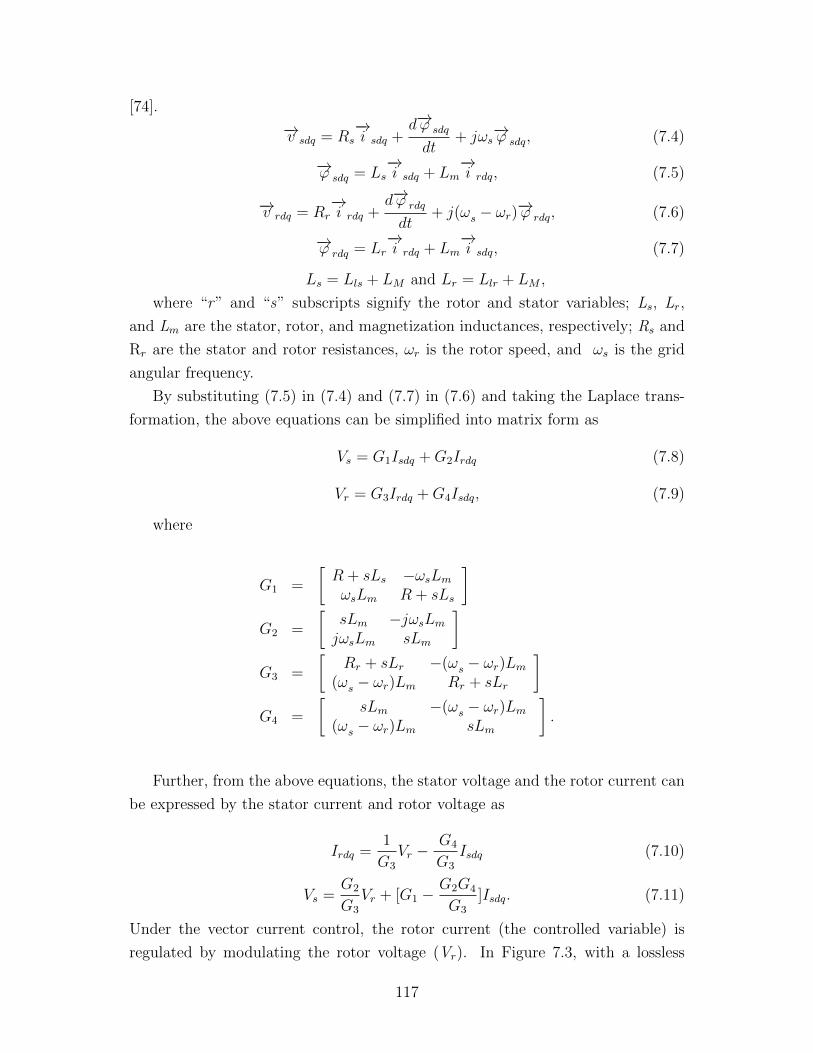
[74].
−→v sdq = Rs−→i sdq +
d−→ϕ sdq
dt+ jωs
−→ϕ sdq, (7.4)
−→ϕ sdq = Ls−→i sdq + Lm
−→i rdq, (7.5)
−→v rdq = Rr−→i rdq +
d−→ϕ rdq
dt+ j(ωs − ωr)
−→ϕ rdq, (7.6)
−→ϕ rdq = Lr−→i rdq + Lm
−→i sdq, (7.7)
Ls = Lls + LM and Lr = Llr + LM ,
where “r” and “s” subscripts signify the rotor and stator variables; Ls, Lr,
and Lm are the stator, rotor, and magnetization inductances, respectively; Rs and
Rr are the stator and rotor resistances, ωr is the rotor speed, and ωs is the grid
angular frequency.
By substituting (7.5) in (7.4) and (7.7) in (7.6) and taking the Laplace trans-
formation, the above equations can be simplified into matrix form as
Vs = G1Isdq +G2Irdq (7.8)
Vr = G3Irdq +G4Isdq, (7.9)
where
G1 =
[R + sLs −ωsLmωsLm R + sLs
]G2 =
[sLm −jωsLmjωsLm sLm
]G3 =
[Rr + sLr −(ωs − ωr)Lm
(ωs − ωr)Lm Rr + sLr
]G4 =
[sLm −(ωs − ωr)Lm
(ωs − ωr)Lm sLm
].
Further, from the above equations, the stator voltage and the rotor current can
be expressed by the stator current and rotor voltage as
Irdq =1
G3
Vr −G4
G3
Isdq (7.10)
Vs =G2
G3
Vr + [G1 −G2G4
G3
]Isdq. (7.11)
Under the vector current control, the rotor current (the controlled variable) is
regulated by modulating the rotor voltage (Vr). In Figure 7.3, with a lossless
117

+
-
sR
ML
si
ssj
sv
slLrlL rsj
rR
rv
( )RSCZ s
Representation of RSC
GSC
( )s
DFIGZ s
Figure 7.4: DFIG impedance circuit.
converter and with the fast operation of modern pulse-width-modulated VSCs, the
output converter voltage can track its reference value very quickly and accurately
(i.e., vr= vrefr ), this yields
Vr= vrefr = Crcc(s)(I
refr − Irdq), (7.12)
where Crcc(s) is the RSC proportional-integral (PI) current controller. By substi-
tuting (7.10) in (7.12)
Vr =Ccc
[1 + Ccc
G3]irefr +
CccG4
G3[1 + Ccc
G3]Isdq. (7.13)
Now by substituting the resulting expression of the rotor voltage in (7.11) can
be expressed as
Vs =
[G2CccG3 + Ccc
]irefr +
[G1 −
G2G4
G3
+CccG4G2
G3[G3 + Ccc]
]︸ ︷︷ ︸
ZsDFIG
Isdq, (7.14)
where ZsDFIG is the output impedance seen from the stator terminal, which repre-
sents the stator, rotor circuits, and the RSC as depicted in Figure 7.4.
The obtained expression reveals that the stator, rotor and rotor-side converter
can be modeled as a Thevenin equivalent circuit. The impedance expression can
be further extended into impedance matrix elements as
ZsDFIG(s) =
[Zs−ddDFIG(s) Zs−qd
DFIG(s)
Zs−dqDFIGC(s) Zs−qq
DFIG(s)
]. (7.15)
For simplicity, the resulting dq-impedance (dc impedance) elements in (7.15) can
also be represented in the phasor domain (ac impedance). The equivalent ac
impedance can be obtained from the dc impedance matrix by replacing (s) by
(s-jωs) [10]
118

m
s
L
L
1
ss j
vsdq
isdq
1
sL
2
1
{ }mr r
s
LL s R
L
2
1
{ }r r m sj L L L
2 { )m s rL L s j
( )r
ccC siref+
-+
-
++
DFIG model
RSC PI-controller
+s
s
R
s j-
Figure 7.5: Block diagram of DFIG current controlled-based.
Zs−ACDFIG(jω) = 0.5[Zs−dd
DFIG (jω − jωs) + Zs−qqDFIG (jω − jωs)
−j(Zs−qdDFIG (jω − jωs) + Zs−dq
DFIG(jω − jωs))].(7.16)
Using the above equations, Figure 7.5 shows the block diagram of a current-
controlled DFIG model.
The equivalent AC impedance of DFIG, in a space vector, including the stator,
and rotor with its controller can be written as [24]
Zs−ACDFIG (jω) = Rs + jXs +
jXm ×(jXr + jω
jω−jωr(Rr + ZRSC)
)jXm +
(jXr + jω
jω−jωr(Rr + ZRSC)
) (7.17)
B) Outer Loop Controllers and Dynamics
The vector control technique is usually used to control a DFIG system. With this
technique, the reference-frame needs to be aligned with a flux linkage in order to
control the rotor currents. In one of the common control alignments, the rotor
currents are controlled by using a synchronously rotating dq-frame aligned with
the stator flux [75]. The d -axis of the rotating reference frame is oriented to the
stator flux. In steady-state and by neglecting the small voltage drop in the stator
resistance, by orientating the direct-axis with the stator flux, the voltage aligns
with the quadrature axis (i.e., vssd = 0), and the active and reactive power of the
stator then can be expressed by
Ps = vssqissq, (7.18a)
Qs = vssqissd. (7.18b)
119
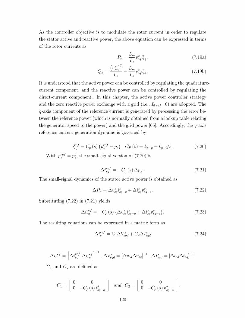
As the controller objective is to modulate the rotor current in order to regulate
the stator active and reactive power, the above equation can be expressed in terms
of the rotor currents as
Ps =LmLs
vssqisrq, (7.19a)
Qs =
(vssq)2
Ls− LmLs
vssqisrd. (7.19b)
It is understood that the active power can be controlled by regulating the quadrature-
current component, and the reactive power can be controlled by regulating the
direct-current component. In this chapter, the active power controller strategy
and the zero reactive power exchange with a grid (i.e., Id ref=0) are adopted. The
q-axis component of the reference current is generated by processing the error be-
tween the reference power (which is normally obtained from a lookup table relating
the generator speed to the power) and the grid power [65]. Accordingly, the q-axis
reference current generation dynamic is governed by
irefrq = Cp (s)(prefs − ps
), CP (s) = kp−p + kp−i/s. (7.20)
With prefs = pos, the small-signal version of (7.20) is
∆irefrq = −Cp (s) ∆ps . (7.21)
The small-signal dynamics of the stator active power is obtained as
∆P s = ∆vssqissq−o + ∆issqv
ssq−o. (7.22)
Substituting (7.22) in (7.21) yields
∆irefrq = −Cp (s) {∆vssqissq−o + ∆issqvssq−o}. (7.23)
The resulting equations can be expressed in a matrix form as
∆irefr = C1∆V ssqd + C2∆Issqd (7.24)
∆irefr =[∆irefrd ∆irefrq
]−1
,∆V ssqd = [∆vsd∆vsq]
−1 ,∆Issqd = [∆ird∆irq]−1.
C 1 and C 2 are defined as
C1 =
[0 00 −Cp (s) issq−o
]and C2 =
[0 00 −Cp (s) vssq−o
].
120
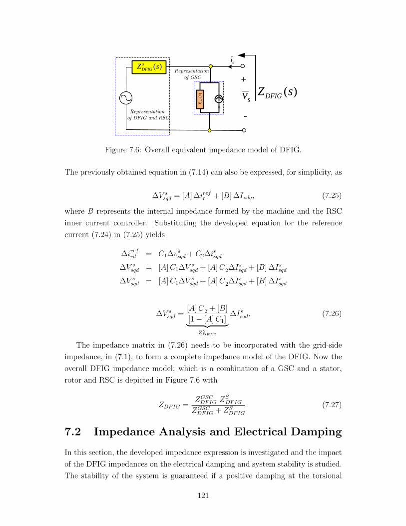
()
GSC
Ys
+
-
si
sv ( )DFIGZ s
Representation of DFIG and RSC
Representation of GSC
( )s
DFIGZ s
Figure 7.6: Overall equivalent impedance model of DFIG.
The previously obtained equation in (7.14) can also be expressed, for simplicity, as
∆V ssqd = [A] ∆irefr + [B] ∆Isdq, (7.25)
where B represents the internal impedance formed by the machine and the RSC
inner current controller. Substituting the developed equation for the reference
current (7.24) in (7.25) yields
∆irefrd = C1∆vssqd + C2∆issqd
∆V ssqd = [A]C1∆V s
sqd + [A]C2∆Issqd + [B] ∆Issqd
∆V ssqd = [A]C1∆V s
sqd + [A]C2∆Issqd + [B] ∆Issqd
∆V ssqd =
[A]C2 + [B]
[1− [A]C1]︸ ︷︷ ︸ZSDFIG
∆Issqd. (7.26)
The impedance matrix in (7.26) needs to be incorporated with the grid-side
impedance, in (7.1), to form a complete impedance model of the DFIG. Now the
overall DFIG impedance model; which is a combination of a GSC and a stator,
rotor and RSC is depicted in Figure 7.6 with
ZDFIG =ZGSCDFIG ZS
DFIG
ZGSCDFIG + ZS
DFIG
. (7.27)
7.2 Impedance Analysis and Electrical Damping
In this section, the developed impedance expression is investigated and the impact
of the DFIG impedances on the electrical damping and system stability is studied.
The stability of the system is guaranteed if a positive damping at the torsional
121

TZ
Synch. genTr. Inf system
Multi-mass mech. sys
Exe Gen LP HP2LX2R
1LX1R
sysXsysR
AC
DC
DC
AC
(IG)
Figure 7.7: System under the study. IEEE SBM with added DFIG.
modes is maintained. Figure 7.7 shows the system under study. This system
uses the data of IEEE SBM [70] with an added DFIG VSC-based system. The
synchronous generator has multi-mass turbines with three torsional modes.
The analysis is conducted for an uncompensated system (as a general power sys-
tem configuration) to identify the impact of the DFIG and its equivalent impedance
on the system damping. By examining the resulting impedance, two key aspects
that actively impact the impedance profile can be identified: the rotor speed and
the controllers’ dynamics.
7.2.1 Base-Case Analysis (DFIG Machine) and MachineOperational Modes
In this section, the controllers are disabled, and only the machine dynamic and its
impedance are considered. Figures 7.8, 7.9 and 7.10 show the phasor (AC) output
impedance, dq-output impedance and the corresponding electrical damping pro-
files with and without adding the DFIG under different rotor speeds (0.35, 0.5,
0.95 and 1.05 p.u.), respectively. The results in the figure reveal that the DFIG
different resistance realization a positive resistance at lower frequency ranges then
become negative closer to the operation rotor speed and become positive after
that rotor speed. This appearance is refected on the damping profile, where the
improvement at the lower frequency is attributed to the positive impedance at the
lower frequency, while the reduction in the damping is due to the negative resis-
tance manifestation before the operational rotor speed. The maximum negative
resistance is manifested in the significant reduction in the damping profile. Gener-
ally, the impact of the DFIG on the damping vanishes as the rotor speed increases.
The impact of the rotor speed is refected in the damping with its complement
(ωs-ωr), the worst-case damping scenario occurs at the lower rotor speeds, as the
complement is refected in the high-frequency range on the damping profile.
The figures also demonstrate the impact of the operational mode of DFIG in the
122

-40
-30
-20
-10
0
10
Ma
gn
itu
de
(d
B)
102
30
60
90
120
Ph
ase
(d
eg
)
Frequency (rad/sec)
Negative impedance
Figure 7.8: DFIG Phasor-impedance (solid: ωr=0.35 p.u.),(dotted: ωr=0.5 p.u.),(dashed: ωr=0.95 p.u) (dashed- dotted: 1.05 p.u.).
0
0.5
1
Ma
g (
p.u
.)
10-1
100
-180
-90
0
90
180
Ph
(d
eg)
r
=0.35 p.u.
Freq (p.u.)
0
0.5
1
Ma
g (
p.u
.)
10-1
100
-180
-90
0
90
180
Ph
(d
eg)
r
=0.50 p.u.
Freq (p.u.)
0
0.5
1
Ma
g (
p.u
.)
10-1
100
-180
-90
0
90
180
Ph
(d
eg
)
r
=0.95 p.u.
Freq (p.u.)
0
0.5
1
Ma
g (
p.u
.)
10-1
100
-180
-90
0
90
180
Ph
(d
eg
)
r
=1.05 p.u.
Freq (p.u.)
Figure 7.9: DFIG dq-impedance (Solid: Zdd and Zqq), (dashed: Zdq) (dotted: Zqd)
123

0 0.1 0.2 0.3 0.4 0.5 0.6 0.7 0.8 0.9 1-2
-1.5
-1
-0.5
0
0.5
1
1.5
2
2.5
3
De
[p.u
.]
Frequency [p.u.]
Figure 7.10: Electrical damping (solid: base-case-no DFIG), (dotted: 0.35 p.u.),(dashed: 0.50 p.u.), (circled: 0.95 p.u.), (dashed-dotted: 1.05 p.u.).
damping profile. Comparing the damping profile at 0.95 p.u. and 1.05 p.u. rotor
speeds, the former represents a sub-synchronous mode and the latter represents
super-synchronous mode. The figure reveals that under super-synchronous mode
DFIG has a positive impact of the damping profile, while in sub-synchronous mode
a reduction in the damping occur in the frequency range just before the operating
rotor speed, however, this impact is disappeared at higher rotor speeds ( ωr>
0.8 p.u.). Comparing between ±5% around the synchronous speed, there is no
significant impact of the operational mode on the damping profile in this case.
The general conclusion from these results is that, the impact of rotor speed on
the impedance profile, hence damping profile becomes negligible with higher rotor
speeds.
7.2.2 Impact of Inner Controller of RSC and GSC Con-verters
Figures 7.11 and 7.12 depict the impedance profile of the DFIG and the damping
profile when the converters (GSC and RSC) are activated. The first impact of
the controller eliminates the peak on the impedance profile created by the rotor
speed. The second impact is that the negative resistance is increased by adding the
converter. By adding the RSC, the range of the negative resistance is prolonged and
the positive impedance appears at (f >0.75 p.u.), whereas without the controllers,
the negative impedance only appears at (0.35 p.u > f >0.75 p.u.). This appearance
refects on the damping profiles, the damping is reduced at low frequency range
124

-30
-20
-10
0
10
20
Ma
gn
itu
de
(d
B)
10-1
100
-90
-45
0
45
90
135
Ph
ase
(d
eg)
Frequency (pu)
Negative impedance
Positive impedance
Figure 7.11: Impedance profile (solid: DFIG without controller) (dotted: DFIGwith only RSC controller) (dashed: DFIG with RSC and GSC controller). Atωr=0.75 p.u.),
and improved at higher frequency range. However, including the GSC improves
the damping as the impedance become more positive with the inclusion of GSC.
In terms of the converter effects, the RSC reduces the positive damping, whereas
including the GSC enhances the damping. Moreover, as the damping plot reveals,
the GSC helps to stabilize the torsional mode no. 2. Generally speaking, the
impact of the controller is dominant over the rotor speed impact.
7.2.3 Impact of Inner Loop Controller Gains
The previous results indicate that the active impedance (the portion of impedance
of the DFIG formed by the controllers) has a significant impact on the overall
equivalent impedance of the DFIG. The key component in the active impedance is
the controller gains. The investigation here reveals that the integral gain does not
have much impact, therefore, the sensitivity of the impedance to the proportional
gain is studied and shown in this subsection. Figure 7.13 shows the damping profile
under the variation of RSC proportional gains (10%, 50% and 100% of the original
value). The impact of the RSC magnifies and appears at the low frequency range.
As the gain increases, the phase angle of the impedance increases. As shown in
Figure 7.14 for the low gain, high improvements are achieved as the phase of the
impedance is reduced (to less than 90o) at the lower frequency range. This result
explains the improvement of the electrical damping at the lower and mid-frequency
ranges.
Similarly, Figure 7.15 shows the impact of the proportional gain of the GSC
125

0 0.2 0.4 0.6 0.8 1-2
-1
0
1
2
3
4
De
[p
.u]
Frequency [p.u.]
Figure 7.12: Impact of GSC and RSC controllers on electrical damping; (solid:DFIG without controller) (dotted: DFIG with only RSC controller) (dashed:DFIG with RSC and GSC controller).
0 0.2 0.4 0.6 0.8 1-2
-1.5
-1
-0.5
0
0.5
1
1.5
2
De
[p
.u.]
Frequency[p.u.]
Figure 7.13: Impact of RSC proportional gain on Electrical damping. (solid: theoriginal gain) (dotted: 50% of the original gain) (dashed: 10% of the original gain)(Original kp=1.26).
126

-40
-30
-20
-10
0
10
Ma
gn
itu
de
(d
B)
101
102
-90
-45
0
45
90
135
Ph
ase
(d
eg)
Frequency (rad/sec)
Negative impedance
Positive impedance
Figure 7.14: Impact of RSC proportional gain on DFIG impedance. (solid: theoriginal gain) (dotted: 50% of the original gain) (dashed: 10% of the original gain).
0 0.2 0.4 0.6 0.8 1-2
-1
0
1
2
3
4
De
[p
.u.]
Frequency [p.u.]
Figure 7.15: Impact of GSC proportional gain on electrical damping. (solid: theoriginal gain) (dotted: 50% of the original gain) (dashed: 10% of the original gain).Original kp=1.0.
127
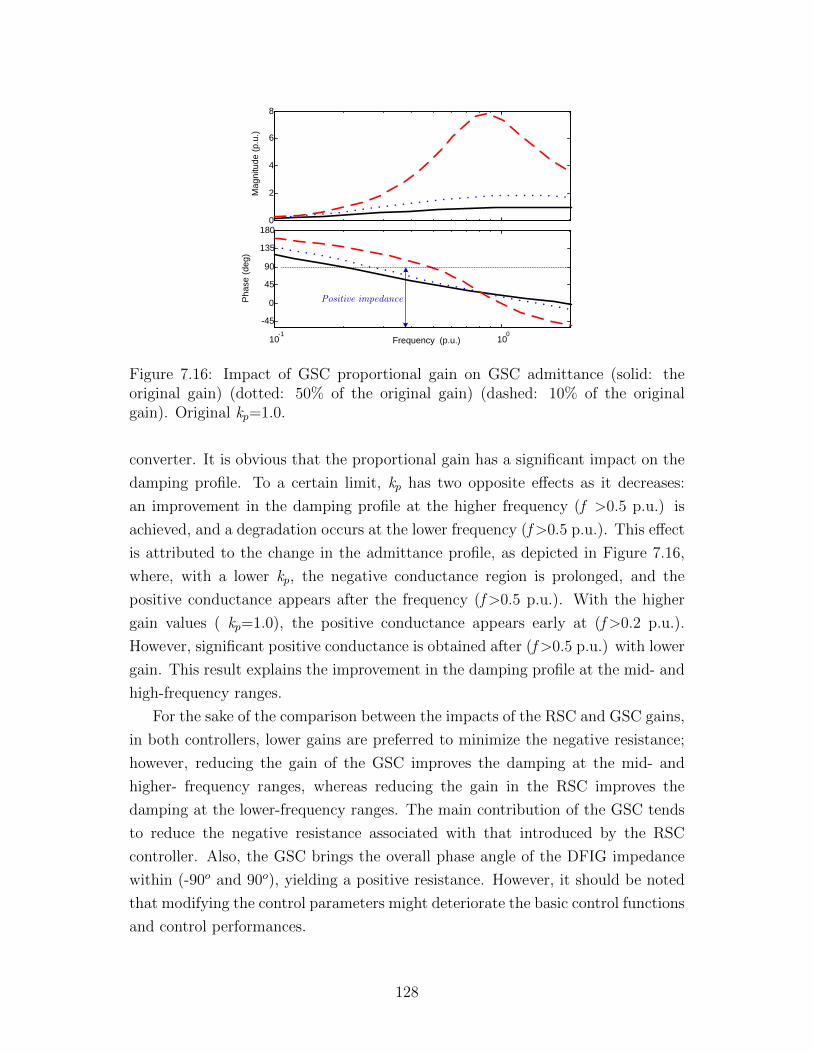
0
2
4
6
8
Ma
gn
itu
de
(p.u
.)
10-1
100
-45
0
45
90
135
180
Ph
ase
(d
eg)
Frequency (p.u.)
Positive impedance
Figure 7.16: Impact of GSC proportional gain on GSC admittance (solid: theoriginal gain) (dotted: 50% of the original gain) (dashed: 10% of the originalgain). Original kp=1.0.
converter. It is obvious that the proportional gain has a significant impact on the
damping profile. To a certain limit, kp has two opposite effects as it decreases:
an improvement in the damping profile at the higher frequency (f >0.5 p.u.) is
achieved, and a degradation occurs at the lower frequency (f>0.5 p.u.). This effect
is attributed to the change in the admittance profile, as depicted in Figure 7.16,
where, with a lower kp, the negative conductance region is prolonged, and the
positive conductance appears after the frequency (f>0.5 p.u.). With the higher
gain values ( kp=1.0), the positive conductance appears early at (f>0.2 p.u.).
However, significant positive conductance is obtained after (f>0.5 p.u.) with lower
gain. This result explains the improvement in the damping profile at the mid- and
high-frequency ranges.
For the sake of the comparison between the impacts of the RSC and GSC gains,
in both controllers, lower gains are preferred to minimize the negative resistance;
however, reducing the gain of the GSC improves the damping at the mid- and
higher- frequency ranges, whereas reducing the gain in the RSC improves the
damping at the lower-frequency ranges. The main contribution of the GSC tends
to reduce the negative resistance associated with that introduced by the RSC
controller. Also, the GSC brings the overall phase angle of the DFIG impedance
within (-90o and 90o), yielding a positive resistance. However, it should be noted
that modifying the control parameters might deteriorate the basic control functions
and control performances.
128
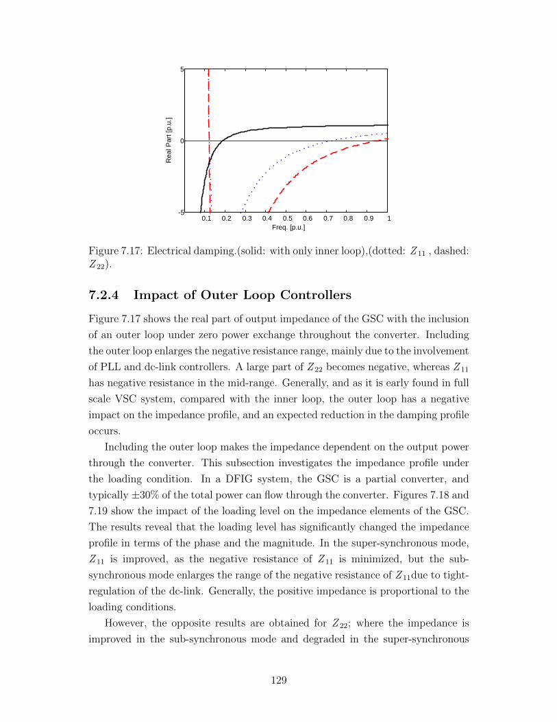
0.1 0.2 0.3 0.4 0.5 0.6 0.7 0.8 0.9 1-5
0
5
Re
al P
art
[p
.u.]
Freq. [p.u.]
Figure 7.17: Electrical damping.(solid: with only inner loop),(dotted: Z 11 , dashed:Z 22).
7.2.4 Impact of Outer Loop Controllers
Figure 7.17 shows the real part of output impedance of the GSC with the inclusion
of an outer loop under zero power exchange throughout the converter. Including
the outer loop enlarges the negative resistance range, mainly due to the involvement
of PLL and dc-link controllers. A large part of Z 22 becomes negative, whereas Z 11
has negative resistance in the mid-range. Generally, and as it is early found in full
scale VSC system, compared with the inner loop, the outer loop has a negative
impact on the impedance profile, and an expected reduction in the damping profile
occurs.
Including the outer loop makes the impedance dependent on the output power
through the converter. This subsection investigates the impedance profile under
the loading condition. In a DFIG system, the GSC is a partial converter, and
typically ±30% of the total power can flow through the converter. Figures 7.18 and
7.19 show the impact of the loading level on the impedance elements of the GSC.
The results reveal that the loading level has significantly changed the impedance
profile in terms of the phase and the magnitude. In the super-synchronous mode,
Z 11 is improved, as the negative resistance of Z 11 is minimized, but the sub-
synchronous mode enlarges the range of the negative resistance of Z 11due to tight-
regulation of the dc-link. Generally, the positive impedance is proportional to the
loading conditions.
However, the opposite results are obtained for Z 22; where the impedance is
improved in the sub-synchronous mode and degraded in the super-synchronous
129

0
5
10
15
20
Ma
gn
itu
de
(p
.u.)
10-1
100
-360
-270
-180
-90
0
90
Ph
ase
(d
eg)
Frequency ([p.u.])
negative resistance
Figure 7.18: Impact of operation mode of DFIG on the Z 11 output impedance.(dotted: P=-0.3 p.u.), (dashed: P=0.3 p.u.), (dotted-dashed: zero power).
0
5
10
Ma
gn
itu
de
(p.u
.)
10-1
100
-360
-270
-180
-90
0
90
Ph
ase
(d
eg
)
Frequency ([p.u.])
negative resistance
Figure 7.19: Impact of operation mode of DFIG on the Z22 output impedance.(dotted: P=-0.3 p.u.) (dashed: P=0.3 p.u.), (dotted-dashed: zero power).
130
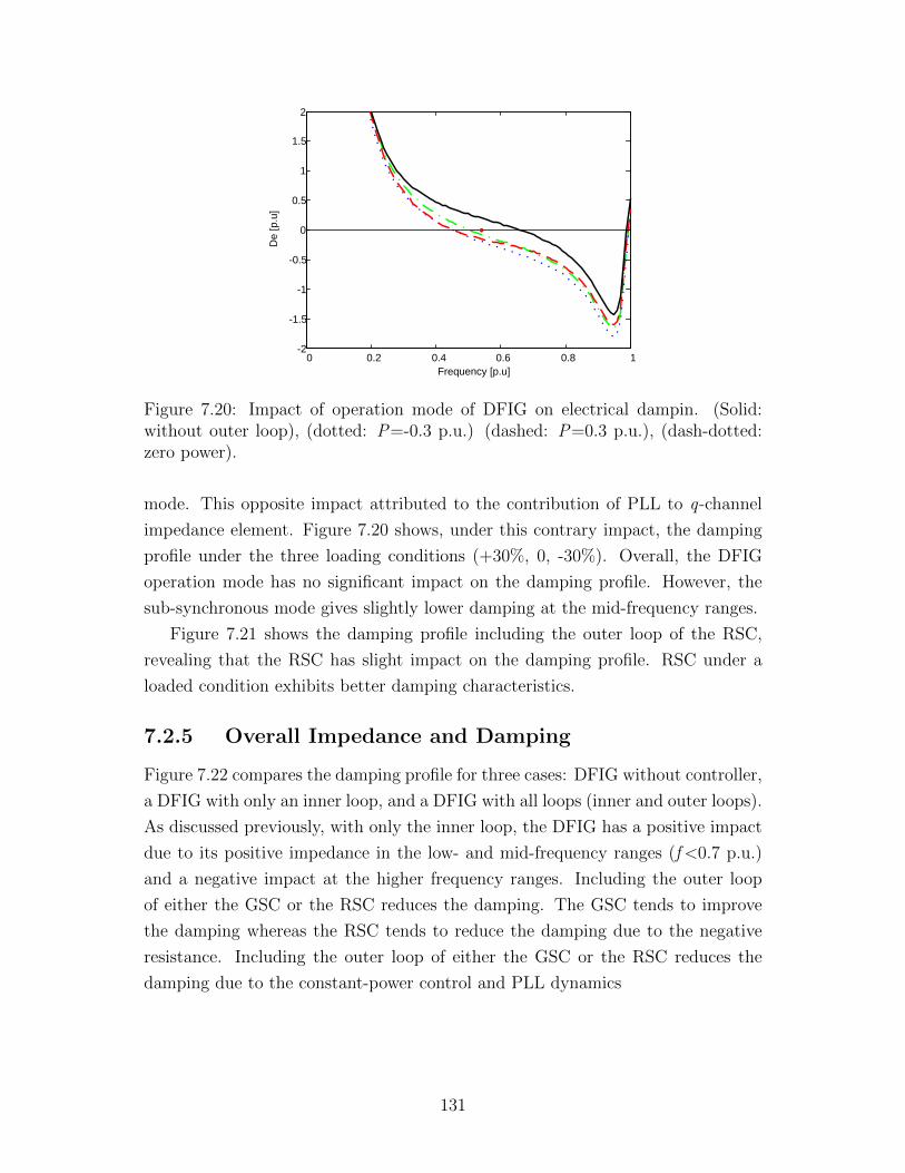
0 0.2 0.4 0.6 0.8 1-2
-1.5
-1
-0.5
0
0.5
1
1.5
2
De
[p.u
]
Frequency [p.u]
Figure 7.20: Impact of operation mode of DFIG on electrical dampin. (Solid:without outer loop), (dotted: P=-0.3 p.u.) (dashed: P=0.3 p.u.), (dash-dotted:zero power).
mode. This opposite impact attributed to the contribution of PLL to q-channel
impedance element. Figure 7.20 shows, under this contrary impact, the damping
profile under the three loading conditions (+30%, 0, -30%). Overall, the DFIG
operation mode has no significant impact on the damping profile. However, the
sub-synchronous mode gives slightly lower damping at the mid-frequency ranges.
Figure 7.21 shows the damping profile including the outer loop of the RSC,
revealing that the RSC has slight impact on the damping profile. RSC under a
loaded condition exhibits better damping characteristics.
7.2.5 Overall Impedance and Damping
Figure 7.22 compares the damping profile for three cases: DFIG without controller,
a DFIG with only an inner loop, and a DFIG with all loops (inner and outer loops).
As discussed previously, with only the inner loop, the DFIG has a positive impact
due to its positive impedance in the low- and mid-frequency ranges (f<0.7 p.u.)
and a negative impact at the higher frequency ranges. Including the outer loop
of either the GSC or the RSC reduces the damping. The GSC tends to improve
the damping whereas the RSC tends to reduce the damping due to the negative
resistance. Including the outer loop of either the GSC or the RSC reduces the
damping due to the constant-power control and PLL dynamics
131
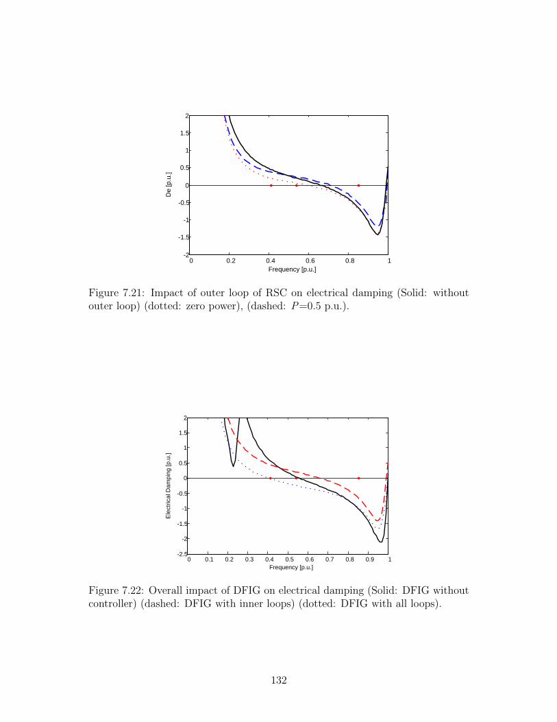
0 0.2 0.4 0.6 0.8 1-2
-1.5
-1
-0.5
0
0.5
1
1.5
2
De
[p.u
.]
Frequency [p.u.]
Figure 7.21: Impact of outer loop of RSC on electrical damping (Solid: withoutouter loop) (dotted: zero power), (dashed: P=0.5 p.u.).
0 0.1 0.2 0.3 0.4 0.5 0.6 0.7 0.8 0.9 1-2.5
-2
-1.5
-1
-0.5
0
0.5
1
1.5
2
Ele
ctr
ica
l D
am
pin
g [p
.u.]
Frequency [p.u.]
Figure 7.22: Overall impact of DFIG on electrical damping (Solid: DFIG withoutcontroller) (dashed: DFIG with inner loops) (dotted: DFIG with all loops).
132

-- ++ i
p
kk
s
ff
ffs
1
Ls R
FF(s)
1/L(s)Ccc(s) Converter(VSC)
Grid Dynamics
ig
vg
iref ++
( )B s
Active impedance controller
+
Converter Dynamics
Figure 7.23: Proposed active damping compensation scheme.
7.3 Proposed Active Damping Compensation
The results from the linear damping analysis reveal that adding the DFIG reduces
the system damping due to negative resistance appearance especially at mid- and
high-frequency range. Under this scenario, active damping technique would be
necessary to enable a stable and reliable integration of a DFIG into a power sys-
tem. The damping compensator could be implemented within the GSC or RSC
control system; the latter seems has some limitation as it involves the machine and
rotor dynamics and might impact the basic maximum power tracking operation of
machine. Alternatively, the GSC offers better flexibility and realization as it inter-
acts directly with the grid. For this purpose, the active impedance compensations,
developed for full-scale VSC in Chapter 4, can be used here to reshape the overall
output impedance of DFIG. Figure 7.23 shows the GSC with the proposed active
damping. Using the developed guidelines previously, the compensator (B(s)) is
designed to operate only in transient conditions and it is chosen to maximize the
positive admittance that appears in the sub-synchronous region, particularly in
the vicinity of the torsional modes.
The modified transfer functions of current controller and the GSC output-
impedance with proposed damping controller can be expressed by
i =
{C (s)
L (s) + C (s)
}︸ ︷︷ ︸
fcc
iref +
{[1−H (s)−B (s)C(s)]
[L (s) + C (s)]
}︸ ︷︷ ︸
Y Newcc
vg, (7.28)
where
B(s) =2ζkcωcs
s2 + 2sζωc + ω2c
.
The modified admittance expressed is obtained as:
133

0
10
20
30
40
Ma
gn
itu
de
(p.u
.)
10-1
100
-45
0
45
90
135
180
225
Ph
ase
(d
eg
)
Frequency ([p.u.])
Y11
Y22
postive resistance
Figure 7.24: Output admittance with proposed active damping. (solid: compen-sated), (dotted: uncompensated).
Y Newcc =
s(s2 + 2sζωc + ω2c ) (s+ ωff ) (Ls2 + kps+ ki) (s+ ωff )
s (s+ ωff ) (s2 + 2sζωc + ω2c )− sωff − 2skζωc(kps+ ki)
. (7.29)
The compensator is designed to eliminate the negative resistance and attain a pos-
itive resistance, hence positive damping in the entire sub-synchronous frequency
range. To achieve this goal the compensator is designed to be band-pass filter
with the following parameters (kc=30 and ωc= 0.8 p.u.). Figure 7.24 compares
between the admittances of the GSC with and without the proposed damping
compensation. It is clear that the proposed technique has improved and reshaped
the admittance profiles; good improvement for Y22 is achievedas it becomes pos-
itive after ( f>0.75 p.u.), and maintains a positive admittance in Y11 element is
the entire sub-synchronous range. Further, the proposed damping magnifies the
admittance magnitude, and overall a positive conductance is obtained. Figure 7.25
compares the damping profile for the worst case (higher negative damping). As
it is clearly shown, the proposed damping is able to improve the damping profile
and maintain a positive damping around the torsional modes of the synchronous
machine.
134

0 0.2 0.4 0.6 0.8 1
-5
0
5
10
Ele
ctr
ica
l D
am
pin
g [p
.u.]
Freq.[p.u.]
Figure 7.25: Electrical damping: (solid: compensated), (dotted: uncompensated),(ωc=.8, kc=50)
7.4 Time-Domain Simulation Results
A detailed time-domain model of the studied system in Figure 7.1 is implemented
in PSCAD/ EMTDCr package to verify the results obtained from the theoretical
impedance and damping analysis. The mechanical torques between masses 1&2,
masses 2&3, and between the exciter and generator are monitored and are shown
in the following results. A transient disturbance (a three- phase fault) occurs at
t=3.0 s for 10 ms. Figure 7.26 shows the torque response when the VSC is not
connected. The system is stable and the torsional modes are damped. The torque
response when the DFIG is connected is shown in Figure 7.27, which reveals that
an oscillatory response is building up as a result of adding the DFIG to the system,
because this addition introduces negative resistance (negative damping) damping
at the torsional frequencies. Figure 7.28 shows the time-domain response with
the proposed active compensation, revealing that it enhances the damping pro-
file and damps sub-synchronous oscillations due to the added positive resistance.
Comparing between the base case (without DFIG) and DFIG with compensation,
the torques response, especially the torque of (LP-Gen), in the latter are more
damped. This result matches the results from the linear analysis.
7.5 Summary
The impact of a DFIG VSC-based on sub-synchronous damping and interactions
has been analyzed in this chapter. A detailed output impedance model of a DFIG
is developed that considered the machine, GSC, and RSC inner and outer controller
loops, and used to study sub-synchronous interactions between a DFIG-VSC and
135
Figure 7.26: Time-domain simulation. Torques response, base-case (withoutDFIG).
Figure 7.27: Time-domain simulation. Torques response with DFIG.
136

T [s] 2.0 3.0 4.0 5.0 6.0 7.0 8.0 ...
...
...
-0.20
-0.10
0.00
0.10
0.20
0.30
0.40
To
rqu
e (
pu
)
HP to LP Torque
-0.20
0.80
To
rqu
e (
pu
)
LP to Gen Torque
0.020
0.030
0.040
0.050
0.060
0.070
0.080
To
rqu
e (
pu
)
Gen to Exc torque
Figure 7.28: Time-domain simulation. Torques response with compensated-DFIG.
an electrically nearby synchronous generator. The impedance profile and electri-
cal damping is examined under different rotor speeds and controller gains. It is
concluded that the impact of the controller dominates over the impact of the ro-
tor speed. The inner controller of the RSC tends to contribute negatively to the
impedance as it enlarges the range of the negative resistance, whereas including the
GSC helps to alleviate the range of the negative resistance. Amongst the controller
loops; the outer loop is the most dominant contributor to the impedance profile.
To facilitate effective DFIG integration into power systems with sub-synchronous
interactions concerns, a simple active damping compensation, based on the local
measurements of the grid voltage at PCC, has been proposed to eliminate the
negative impact resulting from adding DFIG to grid.
137
Chapter 8
Concluding Remarks and FutureWork
8.1 Thesis Conclusions
Integrating voltage source converter (VSC) system into power systems has the
potential to degrade the system damping and create a stability challenge. This
thesis has addressed this challenge by focusing on the sub-synchronous interaction
stability and electrical damping. The key element for the dynamics assessment
of VSCs is the incremental output impedance. This thesis has presented compre-
hensive impedance derivations, analyses, and assessments, and proposed simple
and effective mitigation techniques to eliminate the negative impact of VSCs sys-
tem. Two common VSCs configurations, full-scale and partial-scale (doubly-fed
induction generator (DFIG)) have been considered in this thesis. The impedance
profiles of full-scale VSCs system were also discussed under two different control
topologies: vector control and power synchronization control.
In Chapter 2 , a detailed derivation of the output impedance of full-scale VSCs
was developed. The derivations considered all the grid-side control loops such as
the inner current control, phase-locked loop, and outer loops (direct and quadrature
channels) under all possible control modes and structures.
In Chapter 3, the profile of the output impedance, and hence, also of the
electrical damping, was examined under various control elements and functions.
The impact of the control structure, the control modes, and the output power
levels on the impedance and sub-synchronous electrical damping was investigated
and characterized. Furthermore, the impact of the switching frequency as well
as the bandwidth of the control loops was discussed. The following are the key
findings:
138
1. If only the inner current control loop is considered, the VSC output impedance
becomes independent of the power level of a VSC. The addition of outer
loops yields nonlinear system dynamics that depend on the operating point
and also makes the impedance matrix elements more coupled. Generally
speaking, including the outer loops increases the area of the negative con-
ductance/resistance region.
2. The PLL is one of the main contributors to the negative resistance. The
impact of the PLL appears mainly in the quadrature component of the
impedance (i.e., Z 22). The impact of the PLL depends on the operating
point of the converter. Under the inversion mode (in which VSC delivers
power) negative resistance is manifested in all the sub-synchronous ranges.
However, in the rectification mode, the PLL tends to contribute positively
to the impedance profile.
3. Both Active power and DC-link voltage controls tend to increase the area of
the negative resistance region due to tightly-regulated power control concept,
however, active power control has less impact and has the potential to im-
prove the impedance profile at the low- frequency range. However, the differ-
ence between the controllers appear mainly at low frequencies ( f<0.6 p.u.),
whereas both controllers almost have the same effect at the high-frequency
range ( f<0.6 p.u.)
4. The impact of increasing the switching frequency is manifested in increasing
the overall closed-loop system bandwidths. This factor has two opposite ef-
fects; the increase of the bandwidth of the d -channel improves the impedance
shape and electrical damping, whereas increasing the bandwidth of the PLL
increase the negative resistance in q-channel and further degrades the elec-
trical damping. However, the overall impact seemed to improve the system
damping.
5. Faster current control (i.e., higher bandwidth) has a positive impact on Z 11
in the low-frequency ranges and a negative impact in the high-frequency
range, and also has a negative impact on Z 22. Generally, a higher bandwidth
improves the overall impedance. Therefore, a higher current bandwidth is
recommended to maximize the positive impedance and minimize the negative
interaction at the sub-synchronous frequencies.
6. Reshaping the incremental output impedance by modifying the converter
139
controller parameters is limited by the control performance and bandwidth
requirements. Instead, this thesis proposed several active damping tech-
niques to minimize the negative resistance by using supplementary con-
trollers, which yields a second degree-of-freedom to reshape the converter
impedance, with a minimum effect on the closed-loop control performances
(the tracking and disturbance rejection).
In Chapter 4, three simple and robust active reshaping techniques were pre-
sented. The capability of conventional control system of VSCs showed limited
boundary and effectiveness to shape its output impedance. Instead, reshaping
techniques are proposed by supplementary damping controllers .The reshaping
techniques were realized by modifying the dynamics of the PLL, generating the
stabilizing active impedance via the inner current control, and modifying the dy-
namics of the outer dc-link voltage control loops. The proposed active mitigation
methods showed an excellent performance in reshaping the VSC impedance and
achieving positive impedance and inducing positive electrical damping, which is
necessary to avoid possible sub-synchronous interactions between the VSC system
and the power network. Further, the proposed compensators showed a robust con-
trol performance at different output power levels of the VSC without significant
impact on the converter control performance. With the proposed techniques, the
VSC positively contributes to the damping behaviour in sub-synchronous frequency
range. The effects of the proposed techniques on the tracking and disturbance capa-
bility of the converter were also pointed out. The theoretical analysis, simulation,
and experimental results verified the effectiveness of the proposed techniques.
A novel sub-synchronous torsional damping technique for a series-compensated
system with a multi-mass synchronous generator was proposed in Chapter 5. The
proposed technique was based on reshaping the impedance of the interfacing VSC-
based system to obtain a positive damping in the vicinity of the torsional modes.
In Chapter 6, the output impedance of a VSC system under the newly de-
veloped “power synchronization” control (PSC) was analyzed and presented. It
was observed that under this control, the overall output impedance of the VSC
had non-negative resistance; hence, the VSC system had no negative impact on
the sub-synchronous damping and grid interactions. On the contrary, and com-
pared with the vector current control, the output impedance added damping to
the system under PSC . Different aspects were addressed. The key finding is that;
the loop gain has a linear relationship with the damping. Under only the power
synchronization loop (active power control mode), it was found that the system
140
was stable and apparently had no need for active compensation; however, when
the dc-link voltage controller was used, negative resistance appeared at the lower
frequencies; hence, instability at the lower frequency is possible if the SG has a
torsional mode lies in the negative resistance region. A remedial action with active
compensation might be needed to prevent this instability.
In Chapter 8, the impact of a DFIG VSC-based system on sub-synchronous
damping interactions was analyzed and presented. A detailed output impedance
model of a DFIG was developed. This model considered the machine, grid-side-
converter (GSC), and rotor-side converter (RSC) with the inner and outer con-
troller loops; then it was used to study the sub-synchronous interactions between
a DFIG and an electrically nearby synchronous generator. Several aspects were
considered. The results revealed that the impact of the controller on the impedance
profile dominated over the impact of the rotor speed. The inner controller loop of
the RSC tended to enlarge the range of the negative resistance; however, consider-
ing the inner control loop of the GSC helped to alleviate the range of the negative
resistance. Among the controller loops, the outer loop was the most dominant con-
tributor to the impedance profile. In contrast to the inner loop impact, the GSC
outer loop (the dc-link voltage control) had a negative impact on the impedance,
whereas outer loop of the RSC tended to reduce the area of the negative resistance.
To facilitate the integration of DFIGs into power systems, a simple active damping
compensation based on the local measurement of the grid voltage at the point of
common coupling was proposed to eliminate the negative impact resulting from
adding the DFIG to the grid.
8.2 Suggestions for Future Work
The research work performed and presented in this thesis can be extended in the
following directions:
• VSC-systems can be modeled, implemented and controlled by either rotat-
ing dq-frame or stationary αβ-frame. The former is the most commonly used
technique due to the effectiveness of the control systems implemented in this
frame, and to historical reasons, where power system dynamics are tradition-
ally modeled and analyzed in the dq-frame. One advantage of the αβ-frame
control over the dq-frame control is that the phase-locked loop (PLL) is not
required for frame transformations. This feature reduces the controller bur-
den. Future work could be conducted to study the impedance profile of
141

VSCs with controllers implemented in the αβ-frame, and to investigate the
grid interaction compared with that of the dq-frame control model.
• The focus of the thesis was on the real-part of the output impedance of a VSC
(as an index for damping), with the developed detailed output impedance
(which considered the inner and outer loops, and different control modes);
future work could be conducted to identify and study other stability aspects
of VSC-grid interactions such as VSCs stability in hybrid (ac/dc) systems,
and interactions of VSCs with weak grids.
• With the developed detailed output impedance models, future researches
could study and characterize the sub-synchronous resonance phenomena that
might occur due to the application of series compensated line for long trans-
mission line with a remote and offshore wind turbines ( full-scale and DFIG)
(as a wind resource normally located away and series compensated is used).
• Many studies have shown the potential for the application of PWM current
source converters (CSCs) to renewable resources (i.e., variable speed wind
turbines). The output impedance of CSCs could be derived and analyzed,
and a comparative study with a VSC could be performed.
142
Bibliography
[1] J. M. Carrasco, L.G. Franquelo, and J.T. Bialasiewicz, “Power-electronic
systems for the grid integration of renewable energy sources: A survey,”
IEEE Trans. Ind. Electron., vol. 53, no. 4, pp. 1002–1016, Aug. 2006.
[2] H. Li and Z. Chen, “Overview of different wind generator systems and their
comparisons,” IET Renew. Power Gen., vol. 2, no. 2, pp. 123–138,Jun. 2008
[3] R. C. Portillo, M.M. Prats, and J. I. Leon et al., “Modeling strategy for back-
to-back three-level converters applied to high-power wind turbines,” IEEE
Trans. Ind. Electron., vol. 53, no. 5, pp. 1483–1491, Oct. 2006.
[4] S. B. Kjaer, J. K. Pedersen, and F. Blaabjerg, “A review of single-phase
grid-connected inverters for photovoltaic modules,” IEEE Trans. Ind.Appl.,
vol. 41, no. 5, pp. 1292–1306, Sep./Oct. 2005.
[5] F. Blaabjerg, R. Teodorescu, M. Liserre, and A. V. Timbus, “Overview of
Control and Grid Synchronization for Distributed Power Generation Sys-
tems,” IEEE Transactions on IndustrialElectronics, Vol. 53, No. 5, Oct. 2006,
pp. 1398-1409
[6] Y. Hu, Z. Chen, and H. McKenzie, “Voltage source converters in distributed
generation ystems,” in Proc. 3rd Int. Conf. Electr.Utility Deregul. Restruct.
Power Technol., 2008, pp. 2775–2780.
[7] N. Flourentzou, V. G. Agelidis, and G. D. Demetriades, “VSC-based HVDC
power transmission systems: An overview,” IEEE Trans. Power Electron.
vol. 24, no. 3, pp. 592–602, Mar. 2009.
[8] N. Gibo et al., “Enhancement of continuous operation performance of HVDC
with self-commutated converter,” IEEE Trans. Power Syst., vol. 15, no. 2,
pp. 552–558, May 2000.
143

[9] M. P. Bahrman, E. V. Larsen, H. S. Patel, and R. J. Piwko, “Experience
with HVDC-turbine-generator torsional interaction at Square Butte,” IEEE
Trans. Power App. Syst., vol. PAS-99, pp. 966–975, May/Jun. 1980.
[10] K. R. Padiyar, Analysis of Subsynchronous Resonance in Power Systems.
Boston, MA: Kluwer, 1999.
[11] P. Kundur, Power System Stability and Control. McGraw-Hill, NewYork,
1994
[12] P. M. Anderson, B. L. Agrawal, and J. E. Van Ness, Subsynchronous Reso-
nance in Power Systems. Piscataway, NJ: IEEE Press, 1990.
[13] I. M. Canay, “A novel approach to the torsional interaction and electrical
damping of the synchronous machine. Part I: Theory,” IEEE Trans. Power
App. Syst., vol. PAS-101, no. 10, pp. 3630–3638, Oct. 1982.
[14] A. Tabesh and R. Iravani, “On the application of the complex torque coef-
ficients method to the analysis of torsional dynamics,” IEEE Trans. Energy
Convers., vol. 20, no. 2, pp. 268–275, Jun. 2005.
[15] L. Harnefors, “Analysis of subsynchronous torsional interaction withpower
electronic converters,” IEEE Trans. Power Syst., vol. 22, no. 1,pp. 305–313,
Feb. 2007.
[16] L. Harnefors, “Proof and application of the positive-net-damping stability
criterion,” IEEE Trans. Power Syst., vol. 26, no. 1, pp. 481–482, Feb. 2011.
[17] N. Prabhu and K. R. Padiyar, “Investigation of subsynchronous resonance
with VSC based HVDC transmission systems,” IEEE Trans. Power Del.,
vol. 24, no. 1, pp. 433–440, Jan. 2009.
[18] IEEE SSR Working Group, “First bench mark model for computer simu-
lation of subsynchronous resonance,” IEEE Trans. Power App. Syst., vol.
PAS-96, no. 5, pp.1565–1572, Sep./Oct. 1977.
[19] M. Mohaddes, A. M. Gole, and S. Elez, “Steady state frequency response of
STATCOM,” IEEE Trans. on Power Delivery, vol. 16, pp. 18–23, Jan. 2001.
[20] J. Sun, “Impedance-based stability criterion for grid-connected inverters,
”IEEE Trans. Power Electron., vol. 26, no. 11, pp. 3075–3078,Nov. 2011.
144

[21] M. Cespedes and J. Sun, ”Impedance shaping of three-phase grid-parallel
voltage-source converters,” IEEE Applied Power Electronics Conference and
Exposition (APEC), 2012 Twenty-Seventh Annual, vol., no., pp.754-760, 5-9
Feb. 2012.
[22] L. Harnefors, M. Bongiorno, and S. Lundberg, “Input-admittance calcula-
tion and shaping for controlled voltage-source converters,” IEEE Trans. Ind.
Electron., vol. 54, no. 6, pp. 3323–3334, Dec. 2007.
[23] A. Radwan and Y. Mohamed, “Modeling, analysis, and stabilization of
converter-fed ac microgrids with high penetration of converter-interfaced
loads,” IEEE Trans. Smart Grids, vol. 3, no. 3, pp. 1213–1225, Sep. 2012.
[24] Z. Miao, “Impedance-model-based SSR analysis for type 3 wind generator
and series-compensated network,” IEEE Trans. Energy Conv.,vol. 27, no. 4,
pp. 984–991, Dec. 2012.
[25] L. Xu and L. Fan, ”Impedance-Based Resonance Analysis in a VSC-HVDC
System,” IEEE Transactions on Power Delivery, vol.28, no.4, pp.2209-2216,
Oct. 2013
[26] J. Dannehl, J. M. Liserre, and F. W. Fuchs, “Filter-based active damping of
voltage source converters with LCL filter,” IEEE Trans. Ind. Electron., vol.
58, no. 8, pp. 3623–3633, Aug. 2011.
[27] G. Shen, D. Xu, L. Cao, and X. Zhu, “An improved control strategy for
grid-connected voltage source inverter with LCL filer,” IEEE Trans.Power
Electron., vol. 23, no. 4, pp. 1899–1906, Jul. 2008.
[28] L. Wang and Y. Y. Hsu, “Damping of subsynchronous resonance using exci-
tation controllers and static VAR: a comparison study,” IEEE Trans. Energy
Convers., vol. 3, no. 1, pp. 6–13, Mar. 1988.
[29] N.G. Hingorani and L. Gyugyi, Understanding FACTS: Concepts and tech-
nology of flexible ac transmission system, IEEE Press, NY, 2000.
[30] K. V. Patil, J. Senthil, J. Jiang, and R. M. Mathur, “Application of STAT-
COM for damping torsional oscillations in series compensated AC systems,”
IEEE Trans. Energy Convers., vol. 13, no. 3, pp. 237–243, Sep.1998.
[31] A. E. Hammad and M. El-Sadek, “Application of thyristor controlled Var
compensator for damping sub-synchronous oscillations in power systems,”
145

IEEE Trans. Power App. Syst., vol. PAS-103, no. 1, pp. 198– 212, Jan.
1984.
[32] W. Bo and Z. Yan, “Damping subsynchronous oscillation using UPFC—A
FACTS device,” in Proc. Int. Conf. Power System Technology, vol. 4, pp.
2298–2301, Power Con 2002, Oct. 13–17, 2002.
[33] A. Salemnia, M. Khederzadeh, and A. Ghorbani, “Mitigation of subsyn-
chronous oscillations by 48-pulse VSC STATCOM using remote signal,” in
Proc. IEEE Bucharest PowerTech, vol. 1, pp. 1–7, Jun. 28–Jul. 2, 2009.
[34] K. R. Padiyar and N. Prabhu, “Design and performance evaluation of sub-
synchronous damping controller with STATCOM,” IEEE Trans Power Del.,
vol. 21, pp. 1398–1405, 2006.
[35] B. K. Keshavan and N. Prabhu, “Damping of subsynchronous oscilla-
tions using STATCOM-a FACTS controller,” in Proc. IEEE Conf. Power
Syst.Technol., vol. 1, pp. 12–16, Nov. 21–24, 2004.
[36] M. Bongiorno, L. ngquist, and J. Svensson, “A novel control strategy for
subsynchronous resonance mitigation using SSSC,” IEEE Trans.Power Del.,
, vol.23, no.2, pp.1033-1041,
[37] M. Bongiorno, J. Svensson, and L.Angquist, “Single-phase VSC based SSSC
for subsynchronous resonance damping,” IEEE Trans. Power Del., vol. 23,
no. 3, pp. 1544–1552, Jul. 2008.
[38] S.O. Faried, I. Unal, D. Rai, and J. Mahseredjian, ”Utilizing DFIG-Based
Wind Farms for Damping Subsynchronous Resonance in Nearby Turbine-
Generators,” , IEEE Transactions on Power Systems, vol.28, no.1, pp.452-
459, Feb. 2013.
[39] A.Yazdani and R.Iravani, Voltage-sourced converters in power systems : Mod-
eling, control, and Applications. New Jersey: John Wiley & Sons, 2010.
[40] M. Ashabani and Y.A.-R.I. Mohamed, ”Integrating VSCs to Weak Grids by
Nonlinear Power Damping Controller With Self-Synchronization Capability,”
IEEE Trans. Power Systems, In Press. 2013. [Available online, IEEE Xplore:
doi: 10.1109/TPWRS.2013.2280659]
146

[41] L. Zhang, L. Harnefors, and H.-P. Nee, “Power-synchronization control of
grid-connected voltage-source converters,” IEEE Trans. Power Syst., vol.
25, no. 2, pp. 809–820, May 2010.
[42] A. Ostadi, A. Yazdani, and R. Varma, “Modeling and stability analysis of
a DFIG-based wind-power generator interfaced with a series compensated
line,” IEEE Trans. Power Deivery., vol. 24, no. 3, pp. 1504–1514, Jul. 2009.
[43] L. Fan, C. Zhu, Z. Miao and M. Hu, “Modal Analysis of DFIG-based Wind
Farm Interfaced with a Series Compensated Network,” IEEE Trans. On En-
ergy Conversion, vol. 26, no.4, pp. 1010-1020, Aug. 2011.
[44] L. Fan and Z. Miao, ”Mitigating SSR Using DFIG-Based Wind Genera-
tion,” IEEE Transactions on Sustainable Energy,, vol.3, no.3, pp.349-358,
July 2012
[45] B. Badrzadeh and S. Saylors, ”Susceptibility of Wind Turbine Generators
to Sub-synchronous Control and Torsional Interaction”, in proc. IEEE T&D
conference and exposition, Orlando, USA, May 2012.
[46] G. D. Irwin, A. K. Jindal, and A. L. Isaacs, “Sub-synchronous control inter-
actions between type 3 wind turbines and series compensated ac transmission
systems,” in Proc. IEEE PES General Meeting, Detroit, MI, Jul. 24–28, 2011.
[47] L. Fan and Z. Miao, “Nyquist-stability-criterion-based SSR explanation for
type-3 wind generators,” IEEE Trans. Energy Conv., vol. 27, no. 3, pp. 807–
809, Sep. 2012.
[48] D. H. R. Suriyaarachchi , U. D. Annakkage, C. Karawita, and D. A. Ja-
cobson, ”A Procedure to Study Sub-Synchronous Interactions in Wind In-
tegrated Power Systems,”, IEEE Transactions on Power Systems, vol.28,
no.1, pp.377-384, Feb. 2013
[49] Y. Cheng, M. Sahni, D. Muthumuni , and B. Badrzadeh, ”Reactance Scan
Crossover-Based Approach for Investigating SSCI Concerns for DFIG-Based
Wind Turbines,” , IEEE Transactions on Power Delivery, vol.28, no.2,
pp.742-751, April 2013.
[50] K. Pietilinen, L. Harnefors, A. Petersson, and H.-P. Nee, “DC-link stabi-
lization and voltage sag ride-through of inverter drives,” IEEE Trans. Ind.
Electron., vol. 53, no. 4, pp. 1261–1268, Jun. 2006.
147

[51] A. Emadi, A. Khaligh, C. H. Rivetta and G. Williamson, “Constant power
loads and negative impedance instability in automotive systems: definition,
modeling, stability, and control of power electronic converters and motor
drives,” IEEE Trans. Veh. Technol., vol. 55, no. 4, pp. 1112 – 1125, Jul.
2006.
[52] J. Huang, K. A. Corzine, and M. Belkhayat, “Small-signal impedance mea-
surement of power-electronics-based AC power systems using lineto-line cur-
rent injection,” IEEE Trans. Power Electron., vol. 24, no. 2,pp. 445–455,
Feb. 2009.
[53] V. Valdivia, A. Barrado, A. Lazaro, P. Zumel, C. Raga, and C. Fernandez,
“Simple modeling and identification procedures for ’Black-Box’ behavioral
modeling of power converters based on transient response analysis,” IEEE
Trans. Power Electron., vol. 24, no. 12, pp. 2776–2790, Dec. 2009.
[54] V. Valdivia, A. Lazaro, A. Barrado, P. Zumel, C. Fernandez, and M. Sanz,
“Impedance identification procedure of three-phase balanced voltage source
inverters based on transient response measurements,” IEEE Trans. Power
Electron., vol. 26, no. 12, pp. 3810–3816, Dec. 2011.
[55] S. Chiniforoosh, J. Jatskevic, A. Yazdani, V. Sood, V. Dinavahi, J.
A.Martinez, and A. Ramirez, ”Definitions and applications of dynamic aver-
age models for analysis of power systems,”IEEE Trans. Power Del., vol. 25,
no. 4, pp. 26552669, Oct. 2010
[56] N. Hoffmann, F.W Fuchs, ”Minimal Invasive Equivalent Grid Impedance
Estimation in Inductive–Resistive Power Networks Using Extended Kalman
Filter,” IEEE Trans. Power Electron, vol.29, no.2, pp.631-641, Feb. 2014.
[57] G. Tsourakis, B. M. Nomikos, and C. D. Vournas, “Contribution of doubly
fed wind generators to oscillation damping,” IEEE Trans. Energy Convers.,
vol. 24, no. 3, pp. 783–791, Jul. 2009
[58] M. Mohan, T. M. Undeland, and W. P. Robbins, Power Electronics: Con-
verters, Applications and Design. New York: John Wiley & Sons, Inc., 1989.
[59] A. Grauers, “Efficiency of three wind energy generator systems,” IEEE
Trans. Energy Convers., vol. 11, no. 3, pp. 650–657, Sep. 1996.
148
[60] J. Conroy and R. Watson, “Low-voltage ride-through of a full converter wind
turbine with permanent magnet generator,” IET Renewable Power Genera-
tion, vol. 1, no. 3, pp. 182-189, Sep. 2007
[61] P. Anderson and A. Foud , Power System Control and Stability. Piscataway,
NJ: IEEE Press, 1994.
[62] K. J. strm and T. Hgglund, PID Controllers, 2nd Edition. United States of
America: Instrument Society of America, 1994.
[63] H. Zhang and L. Tolbert, “Efficiency impact of SiC power electronics for
modern wind turbine full scale frequency converter,” IEEE Trans. Ind. Elec-
tron., vol. 58, no. 1, pp. 21–28, Jan. 2011.
[64] R. Ottersten, “On control of back-to-back converters and sensorless induc-
tion machine drives,” Ph.D. dissertation, Chalmers Univ. Technol., Gteborg,
Sweden, 2003.
[65] A. D. Hansen and G. Michalke, “Multi-pole permanent magnet synchronous
generator wind turbines’ grid support capability in uninterrupted operation
during grid faults,” IET Renew. Power Gener., vol. 3, no. 3, pp. 333–348,
Sep. 2009.
[66] E.ON Netz, “Grid Code – High and extra high voltage”, E.ON Netz GmbH,
Bayreuth, 2006
[67] L. Harnefors and H.-P. Nee, “Model-based current control of ac drives using
the internal model control method,” IEEE Trans. Ind. Appl., vol. 34, no. 1,
pp. 133–141, Jan./Feb. 1998.
[68] K. Alawasa, Y.A.-R.I. Mohamed, and W. Xu, ”Modeling, Analysis, and
Suppression of the Impact of Full-Scale Wind-Power Converters on Subsyn-
chronous Damping,” IEEE Systems Journal, , vol.7, no.4, pp.700-712, Dec.
2013.
[69] K. Alawasa, Y.A.-R.I. Mohamed, and W. Xu, ”Active Mitigation of Subsyn-
chronous Interactions Between PWM Voltage-Source Converters and Power
Networks,” IEEE Transactions on Power Electronics, , vol.29, no.1, pp.121-
134, Jan. 2014.
149
[70] IEEE SSR Working Group, ”Second Benchmark Model for Computer Simu-
lation of subsynchronous Resonance”, IEEE Trans. on Power Apparatus and
Systems, Vol. PAS-104, No. 5 1057-1066, 1985.
[71] L. Zhang, H. P. Nee and L. Harnefors, “Analysis of stability limitations of a
VSC-HVDC link using power synchronization control,” IEEE Transactions
on Power Systems, vol. 26, no. 3, pp. 1326-1337, Aug. 2011.
[72] J. B. Hag and D. S. Bernstein, “Non-minimum-phase zeros—much to do
about nothing—classical control—revisited part II,” IEEE Control Syst.
Mag., vol. 27, no. 3, pp. 45–57, Jun. 2006.
[73] S. Skogestad and I. Postlethwaite , Multivariable Feedback Control, 2nd ed.
New York: Wiley, 2005
[74] P.C. Krause, O. Wasynczuk, and S. D. Sudhof, Analysis of electric machinery
and drive systems. New York: IEEE Press, 2013.
[75] W. Leonhard, Control of Electrical Drives, 2nd ed. Berlin, Germany:
Springer-Verlag, 1996.
150

Appendix A
Derivation of Electrical damping
r
dv+
-
fR fL
fi
DiDR
DL
MDL
sRsL q
MDi
+-
di-+
+
-
sRsL
- +
r
qv
GR GL
GiQi
QR
QL
MQL
d
MQi
qi
(a) d-channel (b) q-channel
Figure A.1: dq-model of synchronous machine in rotor reference frame.
Figure 1A depicts the electrical equivalent circuit of a salient pole synchronous
generator in dq-rotor reference frame. In this model, field winding and three
damper windings are considered. The general state space model of a synchronous
machine in the rotor reference frame is described as follows [12]:
i̇ = −L−1 [(R + ωoN) ∆i+ {a1vf + vs}] (A.1)
Te = [T1] [i] (A.2)
where
R = diag (Rd, RD, Rf , Rq, RG, RQ) , vs =[vd vq
]T, is =
[id iq
]T,
i =
idiDifiqiGiQ
, v =
vdvDvfvqvGvQ
, io =
ido0ifoiqo00
, a1 =
100000
, a2 =
0 00 01 00 10 00 0
,
151

T1 =
Ld − Lq −LAQ −LAQ
03x3 LAD 0 0LAD 0 0
LAQ LAQ Ld − Lq0 0 −LAQ 03x3
0 0 −LAQ
L =
LAD + Ls LAD LADLAD LAD + LD LAD 03x3
LAD LAD LAD + LfLAQ + Ls LAQ LAQ
03x3 LAQ LAQ + LG LAQLAQ LAQ LAQ + LQ
N =
Lq −LAQ −LAQ
03x3 0 0 00 0 0
−Ld LAD LAD0 0 0 03x3
0 0 0
Linearization of (A.1) and (A.2) yields
∆̇i = −L−1 (R + ωoN) ∆i− L−1 (R + ∆ωrN)− L−1(∆vs −∆θvso) (A.3)
∆T e = [T1] [∆i] (A.4)
∆is =
[cos ∆θ − sin ∆θsin ∆θ cos ∆θ
][a2] [∆i] (A.5)
The above equations can be re-arranged in a matrix form
∆̇i = [x1]
[∆i∆θ
]+ [x2] ∆ωr + [x3] ∆vs, (A.6)
∆is = [x4]
[∆i∆θ
]] (A.7)
∆T e = [x5]
[∆i∆θ
], (A.8)
x1 =
[−L−1 (R + ωoN) −L−1a2vso
0 0
], (A.9)
152

)(sTeD(s)B(s) C(s)
si sv
A(s)
s)(s r
E(s)
Figure A.2: Electrical damping state-space model.
x2 =
[−L−1Nio
1
], (A.10)
x3 =
[−L−1a2
0
], (A.11)
x4 =[ioT 1 0
], (A.12)
x5 =[aT2 aT2 io
]. (A.13)
Now, the matrix elements in Figure 13(b) can be obtained as follows:
A =x4 (sI−x1) x2, B =x5 (sI−x1) x2
D =x4(sI−x1)x3, C =x5(sI−x1)x3
153

Appendix B
IEEE first benchmark systemdata
IEEE First Benchmark System Data[18]:
• Based value MVA =892.4 and freq= 377 rad/sec.
• Network parameters (pu) : XT = 0.14, R = 0.02, XL = 0.5, Xsys =
0.06
• Generator parameters ( p.u): 892.4 MVA and 24 kV , rs = 0.005, rD =
rG = .025, rQ = rf = 0.025, Lmd = 1.66, Lq = 1.58, Lls = 0.13, Lfl =
0.062, LDl = 0.055, LQl = 0.326, LGl = 0.095
• Multi-Mass Turbine-Generator
Table B.1: IEEE FBM Inertia Constants (p.u.)
Turbine Inertia Constants (pu)
HP Turbine [H1] 0.0929IP Turbine [H2] 0.1556
LPA Turbine [H3] 0.8587LPB Turbine [H4] 0.8842
Generator Turbine [H5] 0.8685Exciter Turbine [H6] 0.0342
• Damping Constants (pu): D1 = D2 = D3 = D4 = D5 = 0.005;
D12 = D23 = D34 = 0.005 and D45 = 0.005
154

Appendix C
IEEE second benchmark systemdata
IEEE Second Benchmark System Data [10] and [70]:
• Based value MVA =100 and freq= 377 rad/sec.
• Network parameters (pu) :
Table C.1: Network parameters (p.u.)XT 0.020RT 0.002R1 0.0074XL1 0.0800R2 0.0067XL2 0.0739Rsys 0.0014Xsys 0.03
• Generator and mechanical system data can be found in[10] and [70].
155

Appendix D
System data
Table D.1 and D.2 show the adopted system data and key parameters in chapter
6 and 7, respectively.
Table D.1: VSC parametersParameters ValueVSC- rated MVA (based) 300 MVADC link voltage 100 kVPhase reactor inductance 0.15 p.u.Phase reactor resistance 0.015 p.u.DC link capacitance 0.3 p.u.Switching Frequency 1980 Hz
Table D.2: DFIG Data (p.u)RatedMVA
100 MVA
Parameters ValueLs 0.09231Lm 3.95279Lr 0.09955Rs 0.0048Rr 0.00549Lg 0.3DC link C 1.0
156