model no: ha-070ziebcaa0-a
TRANSCRIPT

10/7/2019 Page 1 of 19
Model No: HA-070ZIEBCAA0-A
Approved By
Tel: 1 (888) 499-8477 Fax: (407) 273-0771 E-mail: [email protected]: www.microtipsusa.com
HDMI TFT Module Specification
10/7/2019 Page 2 of 19
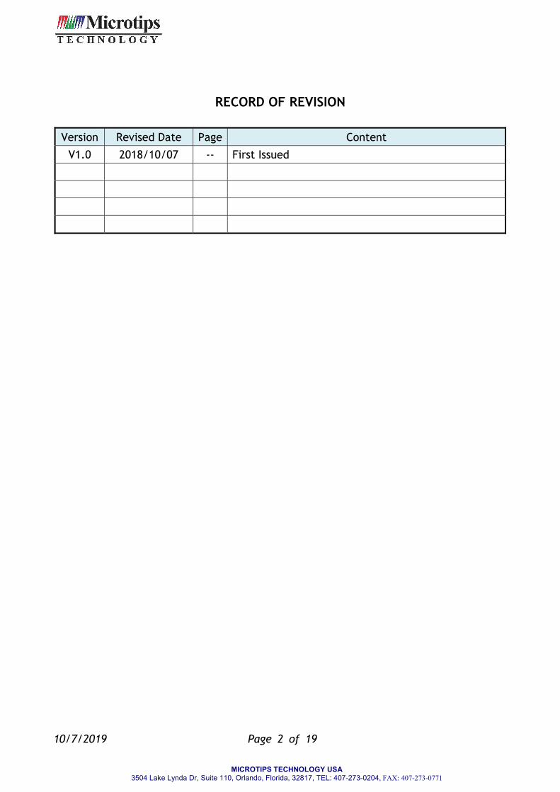
RECORD OF REVISION
Version Revised Date Page Content
V1.0 2018/10/07 -- First Issued
MICROTIPS TECHNOLOGY USA3504 Lake Lynda Dr, Suite 110, Orlando, Florida, 32817, TEL: 407-273-0204, FAX: 407-273-0771

10/7/2019 Page 3 of 19
TABLE OF CONTENTS
No. Content Page
HDMI TFT Module Specification ............................................................ 1
TABLE OF CONTENTS ......................................................................... 3
1. GENERAL DESCRIPTION ............................................................... 4
2. MECHANICAL SPECIFICATION ........................................................ 5
3. PIN DESCRIPTION ...................................................................... 6
4. ABSOLUTE MAXIMUM RATINGS ...................................................... 8
5. BLOCK DIAGRAM ....................................................................... 9
6. ELECTRICAL CHARACTERISTICS ................................................... 10
7. PROJECTED CAPACITIVE TOUCH PANEL SPECIFICATION ...................... 10
8. OPTICAL CHARACTERISTICS ....................................................... 11
9. RELIABILITY ........................................................................... 14
10. PRECAUTION RELATING PRODUCT HANDLING ................................. 19
MICROTIPS TECHNOLOGY USA3504 Lake Lynda Dr, Suite 110, Orlando, Florida, 32817, TEL: 407-273-0204, FAX: 407-273-0771

10/7/2019 Page 4 of 19
1. GENERAL DESCRIPTION
1.1 Description
HA-070ZIEBCAA0-A is a 7.0 (16:10) inch diagonally measured active display with
high resolution WXGA 1280x800 display and high brightness. This model is
composed of a TFT LCD panel, backlight system, a projected capacitive touch
panel and HDMI included Stereo D/A Converter . It is designed to make Raspberry Pi
usage easy. You can simply use this TFT display with your Raspberry Pi, or also you
can use this as computer display with any device which has HDMI output. This 7.0"
TFT model comes in 1280x800 resolution that would be great for embedded
computing usage too.
1.2 Features:
No. Item Specification Unit
1 Panel Size 7” Inch
2 Number of Pixels 1280 (W) x RGB x 800 (H) Pixels
3 Active Area 149.76 (W) × 93.6 (H) mm
4 Pixel Pitch 0.117 (W) x 0.117 (H) mm
5 Outline Dimension 178.76 (W) × 122.6 (H) × 21.7 (T) mm
6 Number of Colors 16.7M - -
7 Display Mode SFT / Normally Black / Transmissive - -
8 View Direction Free direction - -
9 Display Format RGB vertical stripe - -
10 Surface Treatment Clear (7H) - -
11 Contrast Ratio 800 (Typ.) - -
12 Luminance (cd/m^2) 350 (Typ.) cd/m2
13 Video Input Interface HDMI
(Compliance HDMI V1.4 and include HDCP decryption) - -
14 Audio Output Interface Analog Output - -
15 Backlight White LED - -
16 Operation Temperature -20 70 C17 Storage Temperature -30 80 C18 Weight (TBD) g
MICROTIPS TECHNOLOGY USA3504 Lake Lynda Dr, Suite 110, Orlando, Florida, 32817, TEL: 407-273-0204, FAX: 407-273-0771

10/7/2019 Page 5 of 19
2. MECHANICAL SPECIFICATION
MICROTIPS TECHNOLOGY USA3504 Lake Lynda Dr, Suite 110, Orlando, Florida, 32817, TEL: 407-273-0204, FAX: 407-273-0771

10/7/2019 Page 6 of 19
3. PIN DESCRIPTION
3.1 Power Input(CN1) [DC JACK:SCD480CCS000B00GE or compatible]e
3.2 Back-light Control(CN2) [WAFER P2.0mm:2001S-03-RTE or compatible]
Pin No. Symbol I/O Function Note
1 GND P Ground
2 PWM IBack-light Dimming control (internal pull up to 3.3V)
*1
3 LED_EN I No connection. ( internal control)
*1: When PWM, LED_EN not connected, back-light defult is typical brightness.
3.3 Audio line out(CN3) [WAFER P2.0mm:2001S-03-RTE or compatible]
Pin No. Symbol I/O Function Note
1 R_CH A HDMI Audio:Right Channel Analog Output
2 GND P Ground
3 L_CH A HDMI Audio:Left Channel Analog Output
3.4 Standard 3.5mm Phone Jack (CN4) [PHONE JACK:ST-301E or compatible]
HDMI Audio Analog Output
Pin No. Symbol I/O Function Note
1 12V P Power Supply +12V
2 GND P Ground
MICROTIPS TECHNOLOGY USA3504 Lake Lynda Dr, Suite 110, Orlando, Florida, 32817, TEL: 407-273-0204, FAX: 407-273-0771

10/7/2019 Page 7 of 19
3.5 HDMI (CN5) [HDMI A TYPE:PHD0911A2301E or compatible]
Pin No. Symbol I/O Function Note
1 TMDS 2+ I TMDS Data2+
2 GND P TMDS Data2 Shield
3 TMDS 2- I TMDS Data2–
4 TMDS 1+ I TMDS Data1+
5 GND P TMDS Data1 Shield
6 TMDS 1- I TMDS Data1–
7 TMDS 0+ I TMDS Data0+
8 GND P TMDS Data0 Shield
9 TMDS 0- I TMDS Data0–
10 TMDS CLK+
I TMDS Clock+
11 GND P TMDS Clock Shield
12 TMDS CLK-
I TMDS Clock–
13 CEC I CEC
14 N.C. - N.C.
15 DDC_SCL I IIC SCL to EDID ROM
16 DDC_SDA I/O IIC SDA to EDID ROM
17 GND P DDC/CEC Ground
18 HD_5V P +5V Power
19 HPD O Hot Plug Detect
3.6 PCT Control:IIC (CN6) [WAFER P1.25mm:50271-0060L-002 or compatible]
Pin No. Symbol I/O Function Note
1 GND P Ground
2 VDD P Power supply for I2C
3 SCL I IIC SCL to PCT Controller
4 SDA I/O IIC SDA to PCT Controller
5 INT O Interrupt
6 RESET I Reset
MICROTIPS TECHNOLOGY USA3504 Lake Lynda Dr, Suite 110, Orlando, Florida, 32817, TEL: 407-273-0204, FAX: 407-273-0771

10/7/2019 Page 8 of 19
3.7 PCT Control:USB (CN7) [WAFER P1.25mm:50271-0050L-002 or compatible]
Pin No. Symbol I/O Function Note
1 GND
-EARTHP Earth Ground(Shield)
2 VDD_5V P Power supply for USB I/F
3 GND P Power Ground
4 D+ I/O USB data +
5 D- I/O USB data -
3.8 PCT Control:IIC and USB (FPC)
Pin No. Symbol I/O Function Note
1 GND P Ground
2 VDD P Power supply for I2C
3 SCL I IIC SCL to PCT Controller
4 SDA I/O IIC SDA to PCT Controller
5 INT OInterrupt signal to inform the host processor that touch data is ready for read
6 RESET I External low signal reset the chip.
7 VDD_5V P Power supply for USB I/F
8 D+ I/O USB data +
9 D- I/O USB data -
10 GND P Ground
4. ABSOLUTE MAXIMUM RATINGS
4.1 Electrical Absolute Rating
4.1.1 HDMI TFT LCD Module
Item Symbol Values
Unit Note Min Max.
Power supply voltage 12V 10 14 V
4.1.2 Environment Absolute Rating
Item Symbol Values
Unit Note Min Typ Max.
Operating Temperature Top -20 - 70 C Ambient
temperatureStorage Temperature Tst -30 - 80 C
MICROTIPS TECHNOLOGY USA3504 Lake Lynda Dr, Suite 110, Orlando, Florida, 32817, TEL: 407-273-0204, FAX: 407-273-0771

10/7/2019 Page 9 of 19
5. BLOCK DIAGRAM
5.1 TFT LCD Module
1280 x RGB x 800
Source IC+Gate IC
DC/DC Circuit
HDMI to LVDS Bridge
Stereo D/A Converter
Backlight U
nit
12V GND
GND PWM
HDMI Project Touch Panel
VDD VSS /RESET SCL SDA /INT
VDD_5V D+ D- GND
Audio Line out
MICROTIPS TECHNOLOGY USA3504 Lake Lynda Dr, Suite 110, Orlando, Florida, 32817, TEL: 407-273-0204, FAX: 407-273-0771
10/7/2019 Page 10 of 19
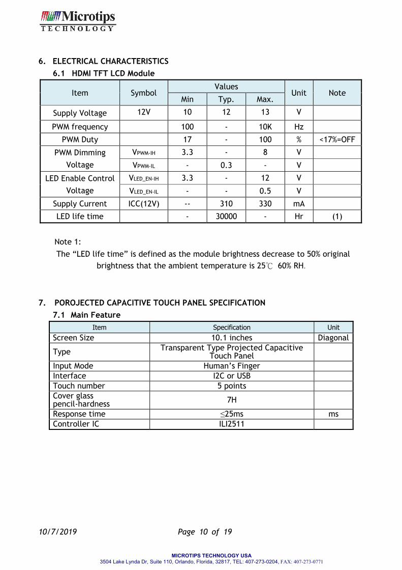
6. ELECTRICAL CHARACTERISTICS
6.1 HDMI TFT LCD Module
Item Symbol Values
Unit Note Min Typ. Max.
Supply Voltage 12V 10 12 13 V
PWM frequency 100 - 10K Hz
PWM Duty 17 - 100 % <17%=OFF
PWM Dimming
Voltage
VPWM-IH 3.3 - 8 V
VPWM-IL - 0.3 - V
LED Enable Control
Voltage
VLED_EN-IH 3.3 - 12 V
VLED_EN-IL - - 0.5 V
Supply Current ICC(12V) -- 310 330 mA
LED life time - 30000 - Hr (1)
Note 1:
The “LED life time” is defined as the module brightness decrease to 50% original
brightness that the ambient temperature is 25℃ 60% RH.
7. POROJECTED CAPACITIVE TOUCH PANEL SPECIFICATION
7.1 Main Feature
Item Specification Unit Screen Size 10.1 inches Diagonal
Type Transparent Type Projected Capacitive
Touch Panel
Input Mode Human’s Finger
Interface I2C or USB
Touch number 5 points
Cover glass pencil-hardness
7H
Response time ≤25ms ms
Controller IC ILI2511
MICROTIPS TECHNOLOGY USA3504 Lake Lynda Dr, Suite 110, Orlando, Florida, 32817, TEL: 407-273-0204, FAX: 407-273-0771

10/7/2019 Page 11 of 19
8. OPTICAL CHARACTERISTICS
Item Symbol Condition Min. Typ. Max. Unit
Brightness --
Note1, Note 3, (θ= 0˚, Normal Viewing Angle)
280 350 -- cd/m2
Uniformity B-uni 70 75 - %
Contrast Ratio CR 600 800 -- --
Response Time Tr
-- 35 40 msTf
Color
Chromaticity White
Wx 0.256 0.306 0.356 --
Wy 0.279 0.329 0.379 --
View angle
Horizontal θx+
Center
CR10
80 88 --
θx- 80 88 --
Vertical θY+ 80 88 --
θY- 80 88 --
Note:The following optical specifications shall be measured in a darkroom or equivalent
state(ambient luminance ≤1 lux, and at room temperature). The operation temperature
is 25˚C±2˚C. The measurement method is shown in Note1.
Note1: The method of optical measurement:
Note2: Measured at the center area of the panel and at the viewing angle of the θx=θy
=0˚
Note3: Definition of Contrast Ratio (CR):
CR = Luminance with all pixels in white state ÷ Luminance with all pixels in Black state
MICROTIPS TECHNOLOGY USA3504 Lake Lynda Dr, Suite 110, Orlando, Florida, 32817, TEL: 407-273-0204, FAX: 407-273-0771

10/7/2019 Page 12 of 19
Note 4: Definition of Viewing Angle:
Note 5: Definition of Brightness Uniformity (B-uni):
B-uni =(Minimum luminance of 9 points÷Maximum luminance of 9points)X100%
MICROTIPS TECHNOLOGY USA3504 Lake Lynda Dr, Suite 110, Orlando, Florida, 32817, TEL: 407-273-0204, FAX: 407-273-0771

10/7/2019 Page 13 of 19
Note 6: Definition of Response Time:
The Response Time is set initially by defining the “Rising Time (Tr)” and the “Falling Time
(Tf)” respectively. Tr and Tf are defined as following figure
Note 7: Definition of Chromaticity:
The color coordinates (Wx,Wy),(Rx,Ry),(Gx,Gy),and (Bx,By) are obtained with all pixels in
the viewing field at white, red, green, and blue states, respectively.
MICROTIPS TECHNOLOGY USA3504 Lake Lynda Dr, Suite 110, Orlando, Florida, 32817, TEL: 407-273-0204, FAX: 407-273-0771

10/7/2019 Page 14 of 19
9. RELIABILITY
9.1 Test Condition9.1.1 Temperature and Humidity(Ambient Temperature)
Temperature : 25 ± 5˚C
Humidity : 65 ± 5%
9.1.2 Operation
Unless specified otherwise, test will be conducted under function state.
9.1.3 ContainerUnless specified otherwise, vibration test will be conducted to the
product itself without putting it in a container.
9.1.4 Test Frequency
In case of related to deterioration such as shock test. It will be
conducted only once.
9.2 TESTS
No. ITEM CONDITION CRITERION
1 High Temperature Storage 80C, 120 hrs
2 Low Temperature Storage -30C, 120 hrs
3 High Temperature Operating 70C, 120 hrs
4 Low Temperature Operating -20C, 120 hrs
5 High Temperature/Humidity
Non-Operating 40C, 90%RH, 120 hrs
6 Temperature Shock Non-Operating-30C 80C(0.5hr each), 100 cycles
7 Vibration Test Non-Operating
Frequency:0 ~ 55 Hz Amplitude:1.5 mm
Sweep Time:11min
Test Period:6 Cycles for each Direction of
X,Y,Z
8 Electro-static Discharge ± 2KV, Human Body Mode, 100pF/1500Ω
Note1: The test sample have recovery time for 24 hours at room temperature before the
function check. In the standard conditions, there is no any touch panel function NG issue
occurred.
MICROTIPS TECHNOLOGY USA3504 Lake Lynda Dr, Suite 110, Orlando, Florida, 32817, TEL: 407-273-0204, FAX: 407-273-0771

10/7/2019 Page 15 of 19
9.3 JUDGMENT STANDARD
The judgment of the above test should be made as follow:
Pass: Normal display image with no obvious non-uniformity and no line defect. Partial
transformation of the module parts should be ignored.
Fail: No display image, obvious non-uniformity, or line defects.
MICROTIPS TECHNOLOGY USA3504 Lake Lynda Dr, Suite 110, Orlando, Florida, 32817, TEL: 407-273-0204, FAX: 407-273-0771

10/7/2019 Page 16 of 19
9.4 INCOMING INSPECTION STANDARDS
MICROTIPS TECHNOLOGY USA3504 Lake Lynda Dr, Suite 110, Orlando, Florida, 32817, TEL: 407-273-0204, FAX: 407-273-0771

10/7/2019 Page 17 of 19
Note1:
(a)Bright point defect is defined as point defect of R,G,B with area >1/2 pixel respectively
(b)Dark point defect is defined as visible in full white pattern.
(c)Definition of distribution of point defect is as follows:
-minimum separation between dark point defects should be larger than 5mm.
-minimum separation between bright point defects should be larger than 5mm.
(d)Definition of joined bright point defect and joined dark point defect are as follows:
-Two or more joined bright point defects must be nil.
-Three joined dark point defects must be nil.
-Coupling of one dark and one bright point in junction is counted as one dark and bright
spot with 1 pair maximum.
-Two Joined dark point is counted as two dark points with 2 pair maximum.
Note2: The external inspection should be conducted at the distance 30± 5cm between the
eyes of inspector and the panel.
Note3: Luminance measurement for contrast ratio is at the distance 50± 5cm between
the detective head and the panel with ambient luminance less than 1 lux. Contrast ratio is
obtained at optimum view angle.
Note4: W-Width in mm , L-length of Max.(L1,L2) in mm.
MICROTIPS TECHNOLOGY USA3504 Lake Lynda Dr, Suite 110, Orlando, Florida, 32817, TEL: 407-273-0204, FAX: 407-273-0771

10/7/2019 Page 18 of 19
9.5 Sampling Condition
Unless otherwise agree in written, the sampling inspection shall be applied to the
incoming inspection of customer.
Lot size: Quantity of shipment lot per model.
Sampling type: normal inspection, single sampling
Sampling table: MIL-STD-105E
Inspection level: Level II
9.6 Inspection conditions
The LCD shall be inspected under 40W white fluorescent light.
θ≤45˚ inspection under non-operating condition.
θ≤5˚ inspection under operating condition
MICROTIPS TECHNOLOGY USA3504 Lake Lynda Dr, Suite 110, Orlando, Florida, 32817, TEL: 407-273-0204, FAX: 407-273-0771

10/7/2019 Page 19 of 19
10. PRECAUTION RELATING PRODUCT HANDLING
10.1 SAFETY
10.1.1 If the LCD panel breaks , be careful not to get the liquid crystal to touch
your skin.
10.1.2 If the liquid crystal touches your skin or clothes , please wash it off
immediately by using soap and water.
10.2 HANDLING
10.2.1 Avoid any strong mechanical shock which can break the glass.
10.2.2 Avoid static electricity which can damage the CMOS LSI—When working
with the module, be sure to ground your body and any electrical
equipment you may be using.
10.2.3 Do not remove the panel or frame from the module.
10.2.4 The polarizing plate of the display is very fragile. So , please handle it very
carefully, Do not touch, push or rub the exposed polarizing with anything
harder than an HB pencil lead (glass , tweezers , etc.)
10.2.5 Do not wipe the polarizing plate with a dry cloth, as it may easily scratch
the surface of plate.
10.2.6 Do not touch the display area with bare hands , this will stain the display
area.
10.2.7 Do not use ketonics solvent & aromatic solvent. Use with a soft cloth
soaked with a cleaning naphtha solvent.
10.2.8 To control temperature and time of soldering is 280 ± 10°C and 3-5 sec.
10.2.9 To avoid liquid (include organic solvent) stained on LCM.
10.3 STORAGE
10.3.1 Store the panel or module in a dark place where the temperature is 25°C ±
5°C and the humidity is below 65% RH.
10.3.2 Do not place the module near organics solvents or corrosive gases.
10.3.3 Do not crush, shake, or jolt the module.
MICROTIPS TECHNOLOGY USA3504 Lake Lynda Dr, Suite 110, Orlando, Florida, 32817, TEL: 407-273-0204, FAX: 407-273-0771