model ep-130 electronic - electronic kits, robot … · i. playground of electronic circuits 11 1....
TRANSCRIPT

ELENCO®
150 Carpenter AvenueWheeling, IL 60090
(847) 541-3800Website: www.elenco.com
e-mail: [email protected]
Copyright © 2012, 2009 by Elenco® Electronics, Inc. All rights reserved. REV-A Revised 2012 753039No part of this book shall be reproduced by any means; electronic, photocopying, or otherwise without written permission from the publisher.
ELECTRONICPLAYGROUNDTM
and LEARNING CENTER
MODEL EP-130
ELENCO®
Wheeling, IL, USA

-159--2-
TABLE OF CONTENTSBefore We Begin Page 4Installing the Batteries 4Making Wire Connections 5Components 5Building Your First Project 9Troubleshooting 10Helpful Suggestions 10
I. PLAYGROUND OF ELECTRONIC CIRCUITS 11
1. Woodpecker 12 2. Police Siren 13 3. Metronome 14 4. Grandfather Clock 15 5. Harp 16 6. Tweeting Bird 17 7. Meowing Cat 18 8. Callin’ Fish 19 9. Strobe Light 20 10. Sound Effects for Horror Movies 21 11. Machine Gun Oscillator 22 12. Motorcycle Mania 23 13. Vision Test 24 14. Patrol Car Siren 25
II. BASIC ELECTRONICS CIRCUITS 26
A MAJOR CHANGE 27 15. Dimming the Light 28 16. Flip Flopping 29 17. Capacitor Discharge Flash 30 18. Transistor Action 31 19. Series and Parallel Capacitors 32 20. Transistor Switching 33 21. Series and Parallel Resistors 34 22. Amplify the Sound 35
III. LED DISPLAY CIRCUITS 36
23. LED Display Basics 37 24. Digital Display Circuit for the Seven-Segment LED 38 25. LED Display with CdS and Transistor 39 26. Switching the LED Display Using Transistor Control 40
IV. WELCOME TO DIGITAL CIRCUITS 41
27. “Flip-Flop” Transistor Circuit 42 28. “Toggle Flip-Flop” Transistor 43 29. “AND” Diode Transistor Logic with LED Display 44 30. “OR” DTL Circuit with Display 45 31. “NAND” DTL Circuit with Display 46 32. “NOR” Transistor Circuit with Display 47 33. “Exclusive OR” DTL Circuit 48
V. MORE FUN WITH DIGITAL CIRCUITS 49
34. “BUFFER” GATE using TTL 50 35. “INVERTER” GATE using TTL 51 36. “AND” GATE using TTL 52 37. “OR” GATE using TTL 53 38. “R-S Flip-Flop” using TTL 54 39. “Triple-Input AND” Gate using TTL 55 40. “AND” Enable Circuit using TTL 56 41. “NAND” Enable Circuit using TTL 57 42. “NOR” Enable Circuit using TTL 58 43. “NAND” Gate Making a Toggle Flip-Flop 59 44. “Exclusive OR” GATE using TTL 60 45. “OR” Enable Circuit using TTL 61 46. Line Selector using TTL 62 47. Data Selector using TTL 63
Important: If you encounter any problems with this kit, DO NOT RETURN TO RETAILER. Call toll-free (800) 533-2441or e-mail us at: [email protected]. Customer Service • 150 Carpenter Ave. • Wheeling, IL 60090 U.S.A.
• Do not short circuit the batteryterminals.
• Never throw batteries in a fire orattempt to open its outer casing.
• Use only 1.5V “AA” type, alkalinebatteries (not included).
• Insert batteries with correct polarity.
• Do not mix alkaline, standard (carbon-zinc), or rechargeable (nickel-cadmium) batteries.
• Non-rechargeable batteries should notbe recharged. Rechargeable batteriesshould only be charged under adultsupervision, and should not berecharged while in the product.
• Do not mix old and new batteries.
• Remove batteries when they are usedup.
• Batteries are harmful if swallowed, sokeep away from small children.
WARNING: Always check your wiring beforeturning on a circuit. Never leave a circuitunattended while the batteries are installed.Never connect additional batteries or anyother power sources to your circuits.
WARNING:CHOKING HAZARD - Small parts.Not for children under 3 years.
Conforms to all applicable U.S. governmentrequirements.
Batteries:
!
IDENTIFYING RESISTOR VALUESUse the following information as a guide in properly identifying the value of resistors.
BANDS
METRIC UNITS AND CONVERSIONS
Abbreviation Means Multiply Unit By Or p pico .000000000001 10-12
n nano .000000001 10-9
μ micro .000001 10-6
m milli .001 10-3
– unit 1 100
k kilo 1,000 103
M mega 1,000,000 106
1. 1,000 pico units = 1 nano unit
2. 1,000 nano units = 1 micro unit
3. 1,000 micro units = 1 milli unit
4. 1,000 milli units = 1 unit
5. 1,000 units = 1 kilo unit
6. 1,000 kilo units = 1 mega unit
IDENTIFYING CAPACITOR VALUESCapacitors will be identified by their capacitance value in pF (picofarads), nF (nanofarads), or μF (microfarads).Most capacitors will have their actual value printed on them. Some capacitors may have their value printed inthe following manner. The maximum operating voltage may also be printed on the capacitor.
Second Digit
First Digit
Multiplier
Tolerance*
Note: The letter “R”may be used at timesto signify a decimalpoint; as in 3R3 = 3.3
103K100V
The letter M indicates a tolerance of +20%The letter K indicates a tolerance of +10%The letter J indicates a tolerance of +5%
Maximum Working Voltage
The value is 10 x 1,000 =10,000pF or .01μF 100V
*
Electrolytic capacitors have a positiveand a negative electrode. The negativelead is indicated on the packaging bya stripe with minus signs and possiblyarrowheads.
Warning:If the capacitoris connectedwith incorrectpolarity, it mayheat up andeither leak, orcause thecapacitor toexplode.
PolarityMarking
BAND 11st Digit
Color DigitBlack 0Brown 1
Red 2Orange 3Yellow 4Green 5Blue 6Violet 7Gray 8White 9
BAND 22nd Digit
Color DigitBlack 0Brown 1Red 2Orange 3Yellow 4Green 5Blue 6Violet 7Gray 8White 9
Multiplier
Color MultiplierBlack 1Brown 10Red 100Orange 1,000Yellow 10,000Green 100,000Blue 1,000,000Silver 0.01Gold 0.1
ResistanceTolerance
Color ToleranceSilver ±10%Gold ±5%Brown ±1%Red ±2%Orange ±3%Green ±0.5%Blue ±0.25%Violet ±0.1%
1 2 Multiplier Tolerance
MultiplierFor the No. 0 1 2 3 4 5 8 9
Multiply By 1 10 100 1k 10k 100k .01 0.1

-158-
Ohm’s Law The relationship betweenvoltage, current, and resistance.
Ohm, (Ω) The unit of measure forresistance.
Oscillator A circuit that uses feedback togenerate an AC output.
Parallel When several electricalcomponents are connectedbetween the same points in thecircuit.
Pico- (p) A prefix used in the metricsystem. It means a millionth ofa millionth (0.000,000,000,001)of something.
Pitch The musical term for frequency.
Printed Circuit Board A board used for mountingelectrical components.Components are connectedusing metal traces “printed” onthe board instead of wires.
Receiver The device which is receiving amessage (usually with radio).
Resistance The electrical friction betweenan electric current and thematerial it is flowing through; theloss of energy from electrons asthey move between atoms ofthe material.
Resistor Components used to control theflow of electricity in a circuit.They are made of carbon.
Resistor-Transistor- A type of circuitLogic (RTL) arrangement used to construct
digital gates.
Reverse-Biased When there is a voltage in thedirection of high-resistanceacross a diode.
Saturation The state of a transistor whenthe circuit resistances, not thetransistor itself, are limiting thecurrent.
Schematic A drawing of an electrical circuitthat uses symbols for all thecomponents.
Semiconductor A material that has more
resistance than conductors butless than insulators. It is used toconstruct diodes, transistors,and integrated circuits.
Series When electrical componentsare connected one after theother.
Short Circuit When wires from different partsof a circuit (or different circuits)connect accidentally.
Silicon The chemical element mostcommonly used as asemiconductor.
Speaker A device which convertselectrical energy into sound.
Switch A device to connect (“closed” or“on”) or disconnect (“open” or“off”) wires in an electric circuit.
Transformer A device which uses two coils tochange the AC voltage andcurrent (increasing one whiledecreasing the other).
Transient Temporary. Used to describeDC changes to circuits.
Transistor An electronic device that uses asmall amount of current tocontrol a large amount ofcurrent.
Transmitter The device which is sending amessage (usually with radio).
Tuning Capacitor A capacitor whose value isvaried by rotating conductiveplates over a dielectric.
Variable Resistor A resistor with an additional armcontact that can move along theresistive material and tap off thedesired resistance.
Voltage A measure of how strong anelectric charge across amaterial is.
Voltage Divider A resistor configuration tocreate a lower voltage.
Volts (V) The unit of measure for voltage.
-3-
VI. MEET TRANSISTOR-TRANSISTOR LOGIC 64
48. Blinking LEDs 65 49. Machiny Sound 66 50. Astable Multivibrator Using TTL 67 51. Tone Generator 68 52. Monster Mouth 69 53. Dark Shooting 70 54. A One-Shot TTL 71 55. Transistor Timer Using TTL 72 56. LED Buzzin’ 73 57. Another LED Buzzin’ 74 58. Set/Reset Buzzer 75 59. Another Set/Reset Buzzer 76
VII. OSCILLATOR APPLICATION CIRCUITS 77
60. Ode to the Pencil Lead Organ 78 61. Double-Transistor Oscillator 79 62. Decimal Point Strobe Light 80 63. “The Early Bird Gets the Worm” 81 64. Adjustable R-C Oscillator 82 65. Heat-Sensitive Oscillator 83 66. Pulse Alarm 84 67. Pushing & Pulling Oscillator 85 68. Slow Shut-off Oscillator 86 69. Electronic Organ Detector 87
VIII. MEET THE OPERATIONAL AMPLIFIER 88
70. Operational Amplifier Comparator 89 71. Changing Input Voltage 90 72. Non-inverting Dual Supply Op Amp 91 73. Inverting Dual Supply Op Amp 92 74. Non-inverting Amplifier 93 75. Dual-Supply Differential Amplifier 94 76. Miller Integrating Circuit 95 77. Stable-Current Source 96 78. Operational Amplifier Blinking LED 97 79. LED Flasher 98 80. Double LED Blinker 99 81. Single Flash Light 100 82. Introducing the Schmitt Trigger 101 83. Initials on LED Display 102 84. Logic Testing Circuit 103 85. Voice-Controlled LED 104 86. Buzzin’ with the Op Amp 105 87. Sweep Oscillator 106 88. Falling Bomb 107 89. Alert Siren 108 90. Crisis Siren 109 91. Op Amp Metronome 110 92. Burglar Buzzer 111
93. LED Initials 112 94. Wake Up Siren 113 95. Voice Activated LED 114 96. Logic Tester 115
IX. MORE FUN WITH OPERATIONAL AMPLIFIERS 116
97. Voice Power Meter 117 98. Reset Circuit 118 99. RC Delay Timer 119 100. Listen To Alternating Current 120 101. Pulse Frequency Multiplier 121 102. White Noise Maker 122 103. Light-Controlled Sound 123 104. DC-DC Converter 124 105. Super Sound Alarm 125 106. Op Amp Three-Input “AND” Gate 126 107. Timer 127 108. Cooking Timer 128
X. RADIO AND COMMUNICATION CIRCUITS 129
109. Operational Amplifier AM Radio 130 110. AM Code Transmitter 131 111. AM Radio Station 132 112. Crystal Set Radio 133 113. Two-Transistor Radio 134 114. Morse Code Oscillator With Tone Control 135
XI. TEST AND MEASUREMENT CIRCUITS 136
115. Water Level Warning 137 116. Water Level Alarm 138 117. Audio Signal Hunter 139 118. RF Signal Tracer 140 119. Square Wave Oscillator 141 120. Sawtooth Oscillator 142 121. Audio Continuity Tester 143 122. Audio Rain Detector 144 123. Audio Metal Detector 145 124. Water Level Buzzer 146 125. Pule Tone Generator 147 126. Resistance Tester 148 127. Transistor Tester 149 128. Sine Wave Oscillator 150 129. Sine Wave Oscillator With Low Distortion 151 130. Twin-T Oscillator 152
INDEX 153
PARTS LIST 155
DEFINITION OF TERMS 156
IDENTIFYING RESISTOR VALUES 159
IDENTIFYING CAPACITOR VALUES 159
METRIC UNITS AND CONVERSIONS 159

-157-
Electric Field The region of electric attractionor repulsion around a constantvoltage. This is usuallyassociated with the dielectric ina capacitor.
Electricity A flow of electrons betweenatoms due to an electricalcharge across the material.
Electrolytic Capacitor A type of capacitor that has highcapacitance and is used mostlyin low frequency circuits. It haspolarity markings.
Electron A sub-atomic particle that hasan electrical charge.
Electronics The science of electricity and itsapplications.
Emitter The output of an NPN bipolarjunction transistor.
Encode To put a message into a formatwhich is easier to transmit.
Farad, (F) The unit of measure forcapacitance.
Feedback To adjust the input to somethingbased on what its output isdoing.
Flip-Flop A type of transistorconfiguration is which the outputchanges every time it receivesan input pulse.
FM Frequency modulation. Thefrequency of the radio signal isvaried depending on the information being sent.
Forward-Biased The state of a diode whencurrent is flowing through it.
Frequency The rate at which somethingrepeats.
Generator A device which uses steam orwater pressure to move amagnet near a wire, creating anelectric current in the wire.
Germanium A chemical element that is usedas a semiconductor.
Ground A common term for the 0V or “–” side of a battery or generator.
Henry (H) The unit of measure forInductance.
Inductance The ability of a wire to create aninduced voltage when thecurrent varies, due to magneticeffects.
Inductor A component that opposeschanges in electrical current.
Integrated Circuit A type of circuit in whichtransistors, diodes, resistors,and capacitors are allconstructed on asemiconductor base.
Kilo- (K) A prefix used in the metricsystem. It means a thousand ofsomething.
Light Emitting Diode A diode made from gallium(LED) arsenide that has a turn-on
energy so high that light isgenerated when current flowsthrough it.
Magnetic Field The region of magneticattraction or repulsion around amagnet or an AC current. This isusually associated with aninductor or transformer.
Magnetism A force of attraction betweencertain metals. Electric currentsalso have magnetic properties.
Meg- (M) A prefix used in the metricsystem. It means a million ofsomething.
Micro- (μ) A prefix used in the metricsystem. It means a millionth(0.000,001) of something.
Microphone A device which converts soundwaves into electrical energy.
Milli- (m) A prefix used in the metricsystem. It means a thousandth(0.001) of something.
Modulation Methods used for encodingradio signals with information.
Morse Code A code used to send messageswith long or short transmitbursts.
NAND Gate A type of digital circuit whichgives a HIGH output if some ofits inputs are LOW.
NPN Negative-Positive-Negative, atype of transistor construction.
Welcome to the thrilling world of electronics! Now thatyou have your Elenco® EP-130 Electronic PlaygroundKit, you can learn about electronics while doing 130fun experiments. In this kit we have includedeverything you will need to start off on this electronicsadventure, well except the batteries that is ☺.
As you go through this manual and do theexperiments, you will notice that we have arrangedthe experiments, as well as information, into a logicalprogression. We will start off with easy circuits andthen work toward the more intricate ones. Take yourtime and be sure to have some fun!
Each electronic component in the kit is connected tosprings, so you can do all the circuit assembly withouthaving to solder. To build a working project, all youhave to do is connect the wires to the terminals asshown in each wiring sequence. There is no dangerwhen doing these projects because you are using lowvoltage batteries, not the standard AC voltages.
Our simple instructions will show you how to operatethe circuit for each experiment. A schematic diagramis also included, to help you learn how the circuitworks. A schematic is simply a blueprint that showshow different parts are wired together. An image orsymbols for each of the components in your kit areprinted next to each piece.
As you will notice we refer to a Volt / Ohm Meter(VOM) for making measurements. A VOM ormultimeter is a instrument that measures voltage,current (amperes or amps), and resistance (ohms-Ω).You will learn more about these in the upcomingpages. If you really want to learn about electroniccircuits, it is vital that that you learn how to measurecircuit values - for only then will you really understandelectronic circuitry.
You do not have to have or use a VOM to do theexperiments but you will find that it helps to bettergrasp how the circuits work. The VOM is a goodinvestment if you plan to stay interested in electricityand electronics.
-4-
BEFORE YOU START THE FUN!
This kit requires six (6) “AA” batteries. To install thebatteries to the back of your kit make sure to installthem in the corresponding compartments. Put the +end and the – end correctly into the kit, the + end forthe battery is the side that has the metal cap.
Remember: Never leave a dying battery or deadbattery in your kit. Even if they are “leak-proof”, theystill have the potential to leak damaging chemicals.
INSTALLATION OF BATTERIES
+
––
+
–
+
+
––
+
–
+
+
––
+
–
+
+
––
+
–
+

-156-
DEFINITION OF TERMS
AC Common abbreviation foralternating current.
Alternating Current A current that is constantlychanging.
AM Amplitude modulation. Theamplitude of the radio signal isvaried depending on theinformation being sent.
Amp Shortened name for ampere.
Ampere (A) The unit of measure for electriccurrent. Commonly shortenedto amp.
Amplitude Strength or level of something.
Analogy A similarity in some ways.
AND Gate A type of digital circuit whichgives a HIGH output only if all ofits inputs are HIGH.
Antenna Inductors used for sending orreceiving radio signals.
Astable Multivibrator A type of transistorconfiguration in which only onetransistor is on at a time.
Atom The smallest particle of achemical element, made up ofelectrons, protons, etc.
Audio Electrical energy represent-ingvoice or music.
Base The controlling input of an NPNbipolar junction transistor.
Battery A device which uses a chemicalreaction to create an electriccharge across a material.
Bias The state of the DC voltagesacross a diode or transistor.
Bipolar Junction A widely used type ofTransistor (BJT) transistor.
Bistable Switch A type of transistorconfiguration, also known as theflip-flop.
Capacitance The ability to store electriccharge.
Capacitor An electrical component thatcan store electrical pressure(voltage) for periods of time.
Carbon A chemical element used tomake resistors.
Clockwise In the direction in which thehands of a clock rotate.
Coil When something is wound in aspiral. In electronics thisdescribes inductors, which arecoiled wires.
Collector The controlled input of an NPNbipolar junction transistor.
Color Code A method for marking resistorsusing colored bands.
Conductor A material that has lowelectrical resistance.
Counter-Clockwise Opposite the direction in whichthe hands of a clock rotate.
Current A measure of how fast electronsare flowing in a wire or how fastwater is flowing in a pipe.
Darlington A transistor configuration whichhas high current gain and inputresistance.
DC Common abbreviation for directcurrent.
Decode To recover a message.
Detector A device or circuit which findssomething.
Diaphragm A flexible wall.
Differential Pair A type of transistorconfiguration.
Digital Circuit A wide range of circuits in whichall inputs and outputs have onlytwo states, such as high/low.
Diode An electronic device that allowscurrent to flow in only onedirection.
Direct Current A current that is constant andnot changing.
Disc Capacitor A type of capacitor that has lowcapacitance and is used mostlyin high frequency circuits.
-5-
Provided in your kit are spring terminals and pre-cutwires, make the wires snap together for your use inthe numerous projects. To join a wire to a springterminal, just directly bend the spring over to one sideand then install the wire into the opening.
When you have to join to two or three wires into asingle spring terminal, be sure that the first wire doesnot come loose when you attach the second and thirdwires. The simplest way to do this is to place thespring onto the opposing side where you haveconnected the first wire.
Only insert the exposed or shiny part of the wire intothe spring terminal. The electrical connection will notbe made if the plastic part of the wire is inserted intothe terminal. Removing the wire from the springterminals is simply just bending each terminal andthen pulling the wires out of it.
If the exposed metal ends of some of the wires breakoff due to great use, you should just simply remove3/8” if the insulation from the wire of the broken endand then simply twist the strands together. To removethe installation you can use either a wire-stripper toolor a simple penknife. Be extremely careful when doingthis because penknives are remarkably sharp.
WIRING CONNECTIONS
This kit has more than 30 distinct components. If thishappens to be your first time with electronics don’t fretover not knowing the difference between a resistor ora transistor, because the general purpose of eachcomponent will be described. The followingexplanations will help you comprehend what eachcomponent does and you will also gain moreknowledge of each component as you do eachexperiment. There is also a parts list in the back ofthis manual, that way you can compare the parts inyour kit with those recorded in the back.
Resistors: Why is the water pipe that goes to thekitchen faucet in your house smaller than the onefrom the water company? And why is the pipe smallerthan the main water line that disburses the water toyour entire town? Because you don’t need a lot ofwater. The pipe size controls the water flow to whatyou really need. Electricity works in the same manner,except that the wires have a minimal resistance thatthey would have to be particularly thin to limit theelectricity flow. They would be solid enough to handleand break effortlessly. However, the flow of waterthrough a large pipe could be restricted to by filling apart of the pipe with rocks (a
COMPONENTS
-155-
PARTS LIST
Bar Antenna with Holder
Battery Box Plastic (2)
Capacitors
10pF, ceramic disc type
100pF, ceramic disc type
0.001μF, ceramic disc type
0.01μF, ceramic disc type
0.02μF, ceramic disc type
0.05μF, ceramic disc type (2)
0.1μF, ceramic disc type
3.3μF, 25V electrolytic type
10μF, 16V electrolytic type
100μF, 10V electrolytic type
470μF, 10V electrolytic type
CdS Cell
CdS Holder Plastic
Digital Display PCB Assembly
LED Digital Display LT-312
PCB for Digital Display
Resistor 360Ω (8)
Diode Germanium 1N34A (2)
Diode Silicon 1SS53 / 1N4148
Earphone, ceramic type
Frame, Plastic (L)
Frame, Plastic (R)
Integrated Circuit 74LS00
Integrated Circuit BA728
Key Switch
Knob, Tuning Capacitor, Plastic
Knob, Control, Metal
Light Emitting Diode (3)
Nut 2mm
Paper Bottom Panel
PCB for 74LS00
PCB for LM358
Resistors
100Ω 5% 1/4W (4)
470Ω 5% 1/4W
1kΩ 5% 1/4W
2.2kΩ 5% 1/4W
4.7kΩ 5% 1/4W
10kΩ 5% 1/4W (2)
22kΩ 5% 1/4W
47kΩ 5% 1/4W
100kΩ 5% 1/4W
220kΩ 5% 1/4W
470kΩ 5% 1/4W
Screw 2.4 x 8mm (4)
Screw 2.5 x 3mm
Screw 2.8 x 8mm (2)
Slide Switch
Speaker, 8Ω
Spring (138)
Transformer
Transistors
2SA733 PNP (2)
2SC945 NPN
Variable Capacitor (tuning)
Variable Resistor (control)
Washer 10mm (4)
Wires
White, 75mm (20)
Red, 150mm (30)
Blue, 250mm (20)
Yellow, 350mm (5)
Black, 380mm (2)
Green, 3M (2)
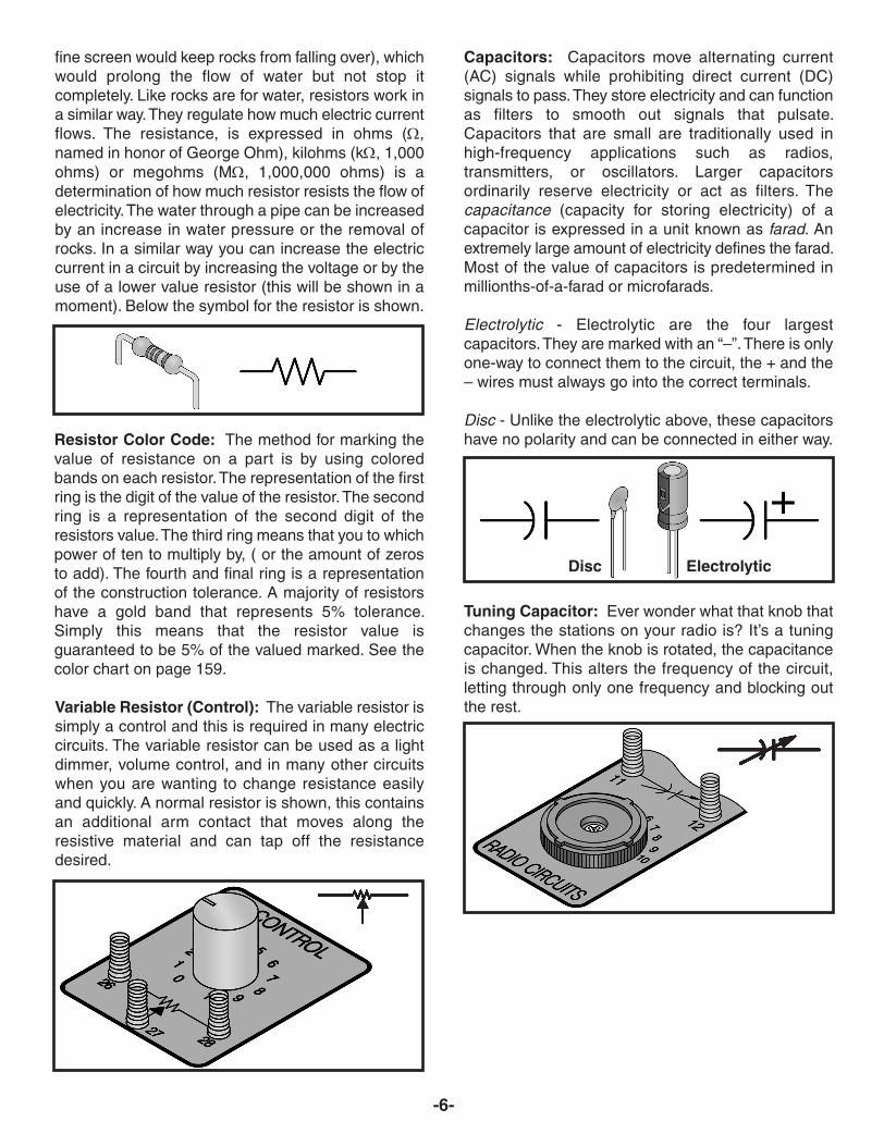
fine screen would keep rocks from falling over), whichwould prolong the flow of water but not stop itcompletely. Like rocks are for water, resistors work ina similar way. They regulate how much electric currentflows. The resistance, is expressed in ohms (Ω,named in honor of George Ohm), kilohms (kΩ, 1,000ohms) or megohms (MΩ, 1,000,000 ohms) is adetermination of how much resistor resists the flow ofelectricity. The water through a pipe can be increasedby an increase in water pressure or the removal ofrocks. In a similar way you can increase the electriccurrent in a circuit by increasing the voltage or by theuse of a lower value resistor (this will be shown in amoment). Below the symbol for the resistor is shown.
Resistor Color Code: The method for marking thevalue of resistance on a part is by using coloredbands on each resistor. The representation of the firstring is the digit of the value of the resistor. The secondring is a representation of the second digit of theresistors value. The third ring means that you to whichpower of ten to multiply by, ( or the amount of zerosto add). The fourth and final ring is a representationof the construction tolerance. A majority of resistorshave a gold band that represents 5% tolerance.Simply this means that the resistor value isguaranteed to be 5% of the valued marked. See thecolor chart on page 159.
Variable Resistor (Control): The variable resistor issimply a control and this is required in many electriccircuits. The variable resistor can be used as a lightdimmer, volume control, and in many other circuitswhen you are wanting to change resistance easilyand quickly. A normal resistor is shown, this containsan additional arm contact that moves along theresistive material and can tap off the resistancedesired.
Capacitors: Capacitors move alternating current(AC) signals while prohibiting direct current (DC)signals to pass. They store electricity and can functionas filters to smooth out signals that pulsate.Capacitors that are small are traditionally used inhigh-frequency applications such as radios,transmitters, or oscillators. Larger capacitorsordinarily reserve electricity or act as filters. Thecapacitance (capacity for storing electricity) of acapacitor is expressed in a unit known as farad. Anextremely large amount of electricity defines the farad.Most of the value of capacitors is predetermined inmillionths-of-a-farad or microfarads.
Electrolytic - Electrolytic are the four largestcapacitors. They are marked with an “–”. There is onlyone-way to connect them to the circuit, the + and the– wires must always go into the correct terminals.
Disc - Unlike the electrolytic above, these capacitorshave no polarity and can be connected in either way.
Tuning Capacitor: Ever wonder what that knob thatchanges the stations on your radio is? It’s a tuningcapacitor. When the knob is rotated, the capacitanceis changed. This alters the frequency of the circuit,letting through only one frequency and blocking outthe rest.
-6-
Disc Electrolytic

-154-
Diodes: Are like one-way streets. They allow thecurrent to flow in only one direction. There are threeof these in your kit. Your kit contains one silicon diode(marked Si) as well as two germanium diodes (markedGe).
Transistors: Three transistors can be found in yourkit. The part that makes each transistor work is a tinychip, which is made of either germanium or silicon.There are a total of three connections points on eachtransistor. They are B, which stands for base, C, whichstands for collector, and E, which stands for emitter.Mainly transistors are used to amplify weak signals.Transistors can also be used as switches to connector disconnect other components as well as oscillatorsto permit signals to flow in pulses.
LEDs (Light Emitting Diodes): These are specialdiodes because they give off light whenever electricitypasses through them. (The current can only passthrough in one direction—similar to “regular” diodes).
LED Digital Display: Seven Light Emitting Diodesare arranged to create an outline that can show mostletters of the English alphabet and all the numbers.An additional LED is added to represent a decimalpoint.
The “8” LED display is mounted on a board and toprevent burning out the display with excess current,permanent resistors have been wired in.
Integrated Circuit: The transistor was invented inthe 1940’s and after that the next big break throughin electronics was in the 1960’s with the inventionintegrated circuit or the ICs. The advantage of this thatthe equivalent of hundreds or even thousands oftransistors, diodes and even resistors can be placedinto one small package.
Two types of ICs are used in this kit. They are thequad two-input NAND and the dual-operationalamplifier, and you will have the chance to learn moreabout these in a bit.
Simple ICs will help you to understand enough tograsp the basic theories of more advanced ICs.
Cadmium Sulfide (CdS) Cell: This is what is knownas a semiconductor, which practically resistselectricity while it conducts. The resistance changesby the amount of light that is shined upon it.
Note: Provided is a light shield to use with the CdScells, to use just simply place the shield over the cell,this helps to prevent light from leaving the cell.
-7-
PNP NPN
LOGIC AND COMPUTER CIRCUITS
AND Gate: 29, 36, 39, 40
Data: 47
DTL: 29, 30, 31, 33, 35
Exclusive OR: 33, 44
Flip-flop: 27, 28, 38, 43, 58, 59
Inverting: 70, 72, 73, 74, 85, 95,109
Line: 46
NAND Gate: 31, 41
NOR Gate: 42
OR Gate: 37, 42, 44, 45
Power Supply: 29, 72, 73, 74, 75
TTL: 34, 35, 36, 37, 38, 39,40, 41, 42, 43, 44, 45,46, 47, 48, 50, 51, 54,55, 60, 78, 90, 112, 123
NATURAL SCIENCE PROJECTS
Electrical Energy: 52
Fish: 11
OSCILLATORS
Blocking: 21
Oscillators: 8, 51
Sine wave: 128, 129, 130
Square wave: 67, 86, 96, 118
SWITCHING AND CONTROL CIRCUITS
Relay: 26
Transistor: 27, 28, 61, 67, 95, 101,113, 127
TEST EQUIPMENT
Transistor Checker: 127
Voltmeters: 25, 68
Water Level: 115
TRANSMITTERS
Code: 110, 114
Tone: 2, 5, 14, 19, 51, 60, 64,65, 66, 94, 110, 111,114, 128, 125
Voice: 4, 52, 85, 97, 105, 111

-153--8-
Antenna: This cylindrical component with a coil offine wire wrapped around it is a radio antenna. Ifyou’re wondering what the dark colored rod is, it’sactually mostly powdered iron. It’s also known as a“Ferrite Core”, which is efficient for antennas, andused in almost all transistor radios.
Transformer: Did you know that if you were to wraptwo wires from different circuits around different endsof an iron bar, and if you were to add current in thefirst circuit, it will magnetically create current in thesecond circuit? That’s exactly what a transformer is!Transformers are used to isolate parts of a circuit, tokeep them from interfering with each other.
If the iron bar in a transformer were allowed to rotate,it would become a motor. However, if a magnet withina coil is rotating then an electrical current is made;this is called a generator. Those two ideas may notseem important but they are the foundation of thepresent society. Pretty much all of the electricity usedin this world is generated by huge generators, whichare propelled by water pressure or steam. Wirestransport energy to homes and businesses where itwill be used. Motors are used to convert the electricityback into mechanical form so that it can be used todrive machinery and appliances.
Speaker: Did you know that electral energy isconverted into sound through a speaker? By using theenergy from an AC electrical signal it createsmechanical vibration. Sound waves, which are
created by variations of vibrations and then travelacross the room. When you hear a sound it is actuallyyour ears feeling the pressure from the air vibrations.To operate a speaker a high current and a low voltageare needed, so the transformer will also be used withthe speaker. (A transformer can convert a high-voltage/low current to a low-voltage/high current).
Similar to the speaker, is the earphone. It is movableand more sensitive than the speaker, otherwise theyare the same. The earphone you will be using isefficient as well as lightweight and can be usedwithout taking away too much electrical energy fromthe circuit. Sound wise you will be using the earphonefor weak sounds and for louder sounds the speakerwill be used.
Batteries: The battery holders that are used in thiskit are constructed to hold six (6) “AA” batteries. Thesebatteries will be the supplier of all the power used inyour experiments. When you connect the wires to thebatteries make sure that you only connect thebatteries to terminals noted. Terminals 119 and 120provide 3 volts while terminals 119 and 121 provide4.5 volts. Be aware that parts can be damaged(burned out) if you connect too much voltage (you canget up to 9 volts from the connections to the batteries)Be sure to make battery connections the right way.
Caution: Make sure your wiring uses the correctpolarity (the “+” and “-” sides of the component)! Someparts can be permanently damaged if you reversepolarity.
INDEXWe’ve added this listing to aid you in findingexperiments and circuits that you might be especiallyinterested in. Many of the experiments are listed two,three, or four times - since they can be used in manyways. You’ll find some listed as entertainment-typecircuits, even through they were not organized thatway in the sequence of projects. However, you mayfind some of these same circuits to be good for otheruses too.
Do you want to learn more about a specific type ofcircuit? Use this Index to look up all the other usesand applications of any specific circuit - then turn tothose and read what we’ve told you in each one. You’llfind by jumping back and forth and around, you oftenwill pick up a lot more circuit details than just by goingfrom one project to the next in sequence.
Use this Index and your own creative ability and weknow you will have a lot of extra fun with your Lab Kit.
BASIC ELECTRONIC CIRCUITS AND COMPONENTS
Capacitors: 6, 11, 12, 16, 17, 19, 21,27, 50, 51, 64, 69, 119,130
Diodes: 29, 31, 34, 79, 91, 101,102, 105, 121
Integrated: 34, 70
Multivibrators: 48, 50, 56, 90, 91
Resistance: 2, 10, 12, 18, 21, 25, 60,74, 77, 78, 94, 102, 114,120, 123, 126
Set / reset: 58, 59
Timing: 4
Transformers: 129
ENTERTAINMENT CIRCUITS
Alarm: 58, 63, 66, 92, 93, 105,107, 116, 120, 123
Audio Oscillators: 51
Buzzin: 56, 57, 92, 107
Code Transmitter: 110
Electronic Cat: 7
Grandfather Clock: 4
Machine Gun: 11
Metal Detector: 123
Metronome: 3, 91
Motorcycle: 12
Musical: 3, 5, 102
Persistence of Vision: 13
Radio: 8, 10, 11, 38, 109, 110,111, 112, 113, 114, 117,118, 123, 124
Rain Detector: 120
RF Signal Tracer: 118
Shot in the Dark: 53
Siren: 2, 14, 15, 87, 88, 89, 90,93
Sound: 1, 2, 3, 4, 5, 6, 8, 10, 11,12, 14, 15, 19, 22, 49, 52,54, 55, 56, 57, 58, 59, 63,64, 66, 72, 87, 88, 89, 90,93, 102, 103, 105, 108
Strobe: 9
Timer: 54, 55, 78, 99, 107, 108,119
INTEGRATED CIRCUIT PROJECTS
Amplifier: 22, 70, 71, 72, 73, 74, 75,76, 77, 78, 79, 80, 81, 82,85, 86, 91, 92, 94, 95, 96,97, 100, 104, 106, 122
Amplifier Uses: 22, 72
IC Radio: 109
LED DISPLAY
LED Display: 13, 16, 18, 20, 23, 24, 25,26, 29, 30, 31, 32, 62, 83,84, 98, 106, 116
Logic: 25, 29, 30, 31, 34, 37, 84,98

-152- -9-
Switch: You know what a switch is – you useswitches every day. When you slide (or flip) to theproper position, the circuit will be completed, allowingcurrent to flow through. In the other position a breakis made, causing the circuit to be “off”. The switch thatwe will be using is a double-pole, double-throw switch.You will learn about that later on.
Key: The key is a simple switch—you press it andelectricity is allowed to flow through the circuit. Whenyou release it, the circuit is not complete because abreak is caused in the circuit’s path. The key will beused in most circuits often times in signaling circuits(you can send Morse code this way as well as otherthings).
Terminals: Two terminals will be used in someprojects (terminals 13 and 14). They will be used tomake connections to external devices such as anearphone, antenna or earth ground connection,special sensor circuits and so forth.
Wires: Wires will be used to make connections to theterminals.
Your parts and spring terminals are mounted on thecolorful platform. You can see how the wires areconnected to the parts and their terminals if you lookunder the platform.
YOUR FIRST PROJECTA simple wiring sequence is listed for each project.Connect the wires with appropriate length betweeneach grouping of terminals listed. When doing theexperiment use the shortest wire that possibly getsthe job done. New groupings will be separated by acomma, connect the terminals in each group.
As an example, here is the project 1 wiring sequence:
1-29, 2-30, 3-104-106, 4-28-124, 5-41-105, 27-88,75-87-103-40, 115-42-119, 76-116, 121-22.Connect a wire between 1 and 29, another wire
between 2 and 30, another between 3 and 104 andthen another wire between 104 and 106. Continueuntil all connections are made.
Caution: The last connection in each wiringsequence is an important power wire; this isdeliberate. It is important that you make thisconnection your LAST connection. Damage can occurif one part of the circuit is completed before another.Therefore follow the wiring sequence exactly.
The twin-T type audio oscillator is very popular foruse with electronic organs and electronic testequipment because it is very stable.
The resistors and capacitors in the twin-T networkdetermine the frequency of oscillation. The letter T isused because the resistors and capacitors arearranged in the shape of the letter T in the schematicdiagram. There are two T networks in parallel acrossfrom each other; hence the term twin is used. Thecapacitors in series shift the phase of the wave; theresistors in series supply voltage to the transistor’sbase as well as shifting the phase of the wave.
Carefully adjust the circuit to obtain pure sine waveoutput as in the previous two projects. Modify thecontrol very slowly over its entire range until you heara tone in the earphone that is very low and resemblesthe lowest note of a large pipe organ. This controlsetting should be between 7 and 10 on your dial.
Once the oscillation has started, adjust the controlcarefully for the setting that gives the purest soundinglow note near the high end of the dial.
You can experiment with this circuit in many ways. Wesuggest you try different values for the 10kΩ and470Ω resistors, and try using higher and lower batteryvoltages. Also, if you have a VOM, try measuringcircuit voltages.
Notes:
EXPERIMENT #130 TWIN-T OSCILLATOR
Schematic
Wiring Sequence:
o 72-106-116-27-124o 28-104-102o 46-103-87o 47-101-86-81-EARPHONEo 48-71o 119-115-82-EARPHONEo 85-88-105o 121-122

-151--10-
SUGGESTIONS TO HELPKeep a Notebook
As you’re about to find out, you are going to learnmany things about electronics by using this kit. As youlearn, many of the things you discover in the easyprojects will be built upon in later projects. We suggestusing a notebook to help you organize the data youwill be collecting.
This notebook does not have to be like the one youuse in school. Think of it more as a fun notebook, thatway you can look back on the all the projects you havedone once you finish.
Wiring Sequence Marking
When you are wiring a project, especially those withlots of connections, you will find it helpful to mark offeach terminal number as you connect the wires to it.Use a pencil and make light marks so that you can goback multiple times and re-read the sequence.
Collecting Components
You should start to make your own collection ofelectronic parts and therefore have your own scrapbox of electronic parts. You can build your own circuitsin or on top of a framework, box or container. Youcould use your circuit as a Science Fair project atschool and even make a major research project fromit.
TROUBLESHOOTINGYou should have no problem with the projects workingproperly if you follow the wiring instructions. However,if you do encounter a problem you can try and fix it byusing the following troubleshooting steps. These stepsare comparable to those steps that electronictechnicians use to troubleshoot complex electronicequipment.
1. Are the batteries being used new? If they are not,this may be your problem because the batteriescould be too weak to power the project.
2. Is the project assembled properly? Check all thewiring connections to make sure that you have allthe terminals wired correctly. Sometimes havingsomeone else look at it helps to find the problem.
3. Are you following the schematic diagram and theexplanation of the circuit? As your understandingand knowledge expands of electronics, you will beable to troubleshoot by following only a schematic,and once you add the description of the circuit youwill be able to figure out your own problems.
4. If you have VOM, try taking some measurementsof the voltage and current. You might be surprisedjust how handy a VOM really is.
5. Try building project 24 (Digital Display Circuit forthe Seven-Segment LED). This is a very simplecircuit that lights part of the LED display using only2 wires.
Contact Elenco® if you still need help.
In this experiment, you build and study a low-distortionsine wave oscillator. Build this experiment after youhave built and studied the previous experimentbecause this one has no transformer; transformersare likely to cause distortion because of their non-linear characteristics.
As in the previous experiment, you should listen to thetone of this oscillator and modify the control for theclearest-sounding single tone (the one with the leastdistortion). Again, start with the control nearmaximum. The operating frequency is about 300Hz atthe minimum distortion setting of the control.
We call this circuit an RC phase shift oscillator, and itis considered a basic sine wave oscillator. The positivefeedback of the signal causes oscillations to occur.The resistors (R) and capacitors (C) make up the pathfor the signal to the transistor base. Every time thesignals pass the RC circuits, a slight time lag occurs.In other words, the rise and fall of the wave (thephase) shifts slightly. That’s why we call it phase shift.After the signal has traveled through the circuit, thephase shifts 180 degrees. When the collector voltagerises, this rise is fed back to the collector with thephase shifted. When the base voltage rises, thecollector voltage falls. This repeating cycle causes thetransistor to oscillate.
The frequency changes when you change the controlsetting, because the degrees of phase shift changes.The tonal quality also changes. Set the control to thepoint where you can hear the purest tone; at this pointa clear sine wave is generated.
Notes:
EXPERIMENT #129: SINE WAVE OSCILLATOR WITH LOW DISTORTION
Wiring Sequence:
o 124-27-48-82-80-EARPHONEo 47-105-93-77-EARPHONEo 81-109-108-28o 94-110-46o 78-138o 79-106-107o 119-137o 121-122
Schematic

-11-
I. PLAYGROUND OF ELECTRONIC CIRCUITS
-150-
This oscillator circuit produces a sine wave signal. Asine wave (or sinusoid) is a wave of pure single-frequency tone. As an example, a 400Hz sine waveis a wave that oscillates 400 cycles in one secondand contains no other frequency contents. Non-sinewaves (such as square wave or triangular wavesignals) have harmonics - waves with frequenciesthat are multiples of the single-frequencyfundamental wave. A non-sine 400Hz wave caninclude the 400Hz wave (its fundamental wave)along with an 800Hz wave (its 2nd harmonic wave)and a 1200Hz wave (its third harmonic wave). Asquare wave signal contains many harmonics.
Experienced technicians can test a circuit by puttinga sine wave into it and listening to its output - andyou can too. If you put in a sine wave, and somethingelse comes out, the undesired harmonic frequenciesmust have been generated somewhere in the circuit.
The key parts of this circuit that produce a 400Hzsine are:
• A 0.1μF capacitor connected across terminals3 and 5 of the transformer. This forms a tankcircuit that resonates at about 600Hz.
• A 470kΩ resistor to turn on the base of thetransistor only a little.
• An adjustable feedback circuit that includes thecontrol and the 0.05μF capacitor.
• A 100Ω resistor connected to the emitter. Thishelps to stabilize the circuit and keep the soundfrom being distorted.
Connect the earphone to terminals 1 and 2 of thetransformer. Start with the control on maximum (10on the dial) and slowly decrease the control settingwhile listening to the tone quality of the output. Beforethe oscillations stop, you will reach a point where youhear only one tone. This last clear-sounding tone isthe sine wave. Repeat these control adjustments untilyou have no trouble distinguishing between a sinewave and a distorted wave.
Notes:
EXPERIMENT #128: SINE WAVE OSCILLATOR
Schematic
Wiring Sequence:
o 1-EARPHONEo 2-EARPHONEo 3-28-109o 4-94-106-124o 5-41-110o 26-40-93o 27-105o 42-71o 72-119o 121-122

-149--12-
Transistors are very important, and you may need totest them to be sure they are working. You can’t tell ifone is working just by looking at it, but this circuit letsyou test them. This circuit also checks whether atransistor is a PNP or an NPN.
You’ll notice that this project has three long wires - onefor the emitter, one for the collector and one for thebase. The schematic shows the terminals marked forchecking PNP transistors.
To use this experiment, connect the long wires to thebase, collector, and emitter of the transistor you wantto test. Turn the control fully counter-clockwise. Then,press the key and turn the control clockwise. Thetransistor is a working PNP transistor if you hear asound from the speaker. If you hear no sound at all,change connections 4-124 and 119-138 to 4-119 and124-138, and repeat the test. If you get a sound fromthe speaker this time, the transistor is a working NPNtype. If you get no sound from the speaker using eitherset of connections, the transistor is defective.
You’ll find this a handy circuit for testing unmarkedtransistors as you start to accumulate parts for otherelectronic circuits.
Notes:
EXPERIMENT #127: TRANSISTOR TESTER
Schematic
Wiring Sequence:
o 1-29o 2-30o 3-105-COLLECTORo 4-124o 5-94-106-110o 26-72-137o 27-71o 28-EMITTERo 93-109-BASEo 119-138o 121-122
For your first experiment you are going to make acircuit that that sounds like a woodpecker chirping.Follow the wiring sequence carefully and observe thedrawings. Don’t forget to make all the properconnections and have fun!
The simple circuit shown here does not have a keyor a switch, but you can easily add one. Replaceconnection 124-28 with connections 124-137 and138-28 to connect the key. Or, you can hook theswitch up by replacing 124-28 with connections 124-131 and 132-28. Now you can easily turn off and onthe circuit. Go outside and see if you can attract birdswith it.
Want a different sound? Try varied combinations ofcapacitance and resistance in place of the 100μFcapacitor and the 1kΩ resistor. To change the 100μFcapacitor to 470µF, disconnect terminal 116 andtransfer to terminal 118. Then, reconnect the wirefrom 115 to connect to 117. Your “bird” might soundlike a cricket, or a bear!
Also, you can try using the 3V power supply.Disconnect terminal 119 and connect it to terminal123. Now your bird might sound like an Englishsparrow. Feel free to experiment. Just don’t replacethe 47kΩ resistor with anything below 10kΩ,because it might damage the transistor.
Notes:
EXPERIMENT #1: WOODPECKER
Wiring Sequence:
o 1-29o 2-30o 3-104-106o 4-28-124o 5-41-105o 27-88o 75-87-103-40o 115-42-119o 76-116o 121-122
Schematic

-148- -13-
Here is the first siren you are going to do – don’t beshocked if this experiment becomes the most famouscircuit in this kit.
This siren sounds like a real siren on a police car!After the wiring is competed press the key. The toneyou eventually hear gets higher after pressing thekey. When you release the key, the tone gets lowerand then fades out.
Try some of these modifications:
1. If you change the 10μF capacitor to a 100μF or a470μF it will give a very long delay for both turnoff and turn on.
2. Change the circuit to remove the delays bytemporarily disconnecting the 10μF capacitor.
3. Change out the 0.02μF capacitor to a 0.01μFcapacitor, and then to a 0.05μF capacitor.
Notes:
EXPERIMENT #2: POLICE SIREN
Wiring Sequence:
o 1-29o 2-30o 3-103-109o 4-119-137o 5-47-110o 46-104-90o 114-48-120o 85-138o 86-89-113
If you use a meter you can find the exact value of aresistance; but when you only want to knowapproximate resistance values, you can use thisresistance tester.
This circuit converts resistance to electric current andcompares it with the comparator’s reference currentto tell you the approximate range of resistance. Thecomparator has a reference voltage of about 0.82V.
Build the circuit and set the switch to position A.Connect the material to be tested between terminals13 and 14. The LED lights if the resistance is lessthan 100kΩ, otherwise it is off. If the LED lights,connect terminals 93 and 86. If the LED turns off nowthe resistance is between 10Ω and 100kΩ. If it stayson, remove the wire from terminal 86 and connect itto terminal 84. If the LED turns off now, theresistance is in the range of 1 to 10kΩ. If the LED stilldoesn’t turn off, remove the wire from terminal 84and connect it to terminal 76. If the LED turns offnow, it means that the resistance is in the range of100Ω to 1kΩ; if it stays on, the resistance is less than100Ω.
Notes:
EXPERIMENT #126: RESISTANCE TESTER
Schematic
Wiring Sequence:
o 13-93-69-WIREo 14-79-70-121o 75-83-94-90-88-31-63-131o 33-67o 68-80-87o 85-89o 119-124o 122-132
Schematic

-147--14-
Learning to play a musical instrument? Then youmight find this experiment helpful. This is anelectronic version of the metronome, used by musicalstudents and musical geniuses alike, worldwide.
If you press the key, you hear a repeating sound fromthe speaker. Turn the control knob to the right andyou’ll hear the sound “get faster” as the time betweensounds shortens.
Try swapping out the 4.7kΩ resistor with differentone. Also, you might want to try a different capacitorin place of the 100μF capacitor too see what effect itwill have. Are you still keeping notes?
If you would like to hear the difference that a strongercapacitor makes, try connecting the 470μF capacitorto the batteries. Connect terminal 117 to 119 andterminal 118 to terminal 120. You might need toadjust the control to maintain the same pulse rate.
Notes:
EXPERIMENT #3: METRONOME
Wiring Sequence:
o 1-29o 2-30o 3-104-116o 4-28-138o 5-41-103o 27-80o 40-115-79o 42-119o 120-137
Schematic
This experiment is a pulse-tone oscillator with anadjustable frequency that can obtain a wide range ofnotes. You can play tunes on it that sound like anelectronic organ, but it takes some practice.
To play a tune, modify the control to the proper noteand press the key. Readjust the control for the nextnote and press the key again.
When you close the key the first time, the basecurrent flows around the loop formed by the battery,the 10kΩ resistor, the 50kΩ resistor, the transistorbase and emitter, and the key.
The base current causes the collector current to flowaround the loop formed by the 3V supply, the lowerhalf of the transformer winding, the transistorcollector and emitter, and the key.
The current through the transformer causes a currentto flow around the loop formed by the top transformerwinding, the 0.05μF capacitor, the transistor baseand emitter, the key, the battery and back to thetransformer’s center terminal (terminal 4). Thiscurrent quickly (in less than 0.0001 seconds)charges the 0.05μF to about 4V or so with a polaritynegative on the transformer side and positive on thetransistor base lead side. The speaker is onlyactivated while the current flows in the transformer.
When the induced voltage from the top half of thetransformer winding stops, the charging of the0.05μF capacitor stops, then the capacitor begins tocharge again. As soon as the discharge begins, thecapacitor voltage becomes higher than the batteryvoltage. The reverse polarity voltage is applied to thebase and the transistor turns off. Now, all transistorjunctions act as open circuits. The capacitordischarges around the loop formed by the toptransformer winding, the 10kΩ resistor, and the 50kΩresistor. When you reduce the control setting, thedischarge is faster, so the process is repeated at afaster rate causing a higher frequency. The cyclerepeats when the 0.05μF capacitor discharges toslightly below the 3V of the battery.
Notes:
EXPERIMENT #125: PULSE TONE GENERATOR
Schematic
Wiring Sequence:
o 1-29o 2-30o 3-108-110o 4-82-120o 27-40-107o 28-81o 5-41-109o 42-137o 119-138

-146- -15-
Does your home lack a grandfather clock? Well notany longer, with this experiment you will make yourown electronic grandfather clock.
This circuit will produce clicks at approximately one-second intervals. The sound and timing togethermight remind you of an old grandfather clock. If youwould like for it to go faster or slower then you canchange out the 100kΩ resistor.
The steady ticking can put animals (and people) intoa sleepy state of mind. If you have ever traveled on atrain, you remember how sleepy you get fromhearing the clicking sound of the wheels.
Ever scare a clock out of ticking? Shout directly intothe speaker. You can briefly stop the clock! Thespeaker acts like a microphone as well. The soundof your voice vibrates the speaker and disturbs theelectrical balance of the circuit, briefly.
Notes:
EXPERIMENT #4: GRANDFATHER CLOCK
Wiring Sequence:
o 1-29o 2-30o 3-104-116o 4-90-120o 5-41-103o 40-72o 42-119o 71-89-115
Schematic
You can use the operational amplifier as acomparator for detecting changes in voltage. In thisexperiment, you are going to use this comparatorfunction to make a water buzzer that sounds whenthe wire ends come into contact with water.
Slide the switch to position B, build the circuit, andthen slide the switch to position A to turn on thecircuit. You should not hear any sound from thespeaker. Now connect the two output terminals witha wire, and you hear a sound from the speaker.
Touch the two output terminals with your fingers. Ifthe speaker makes a sound again, the electricity isflowing through your body because the wire lead isin contact with sweat.
This experiment uses two operational amplifiers. IC1 works as a comparator. The IC’s negative (–) inputterminal has a reference voltage of about 1.6V. Whena voltage exceeding 1.6V is applied to the positive(+) input terminal, the output of the comparatorallows IC 2 to work as an astable multivibrator.
Notes:
EXPERIMENT #124: WATER LEVEL BUZZER
Wiring Sequence:
o 1-29o 2-30o 3-114o 5-83-80-94-70-110-121o 13-86-63-131o 14-93-69o 65-89-109o 66-82-84-91o 64-90-92-113o 67-81o 68-79-85o 119-124
Schematic

-145--16-
Have you ever wanted to make music just by wavingyour hand? Well that is just what you are going to bedoing. How does this magic work? Well, the toneschange based upon the amount of light that gets tothe CdS cell. With a bright light the tone is higher but,if you cover the CdS with your hand, the sound getslower.
Since the early days of vacuum-tube circuitry, thismethod of creating musical sound has been used.Leon Theremin was the inventor of this type ofinstrument, thus the instrument has been named theTheremin in his honor.
After the wiring has been completed press the keyand then wave your hand over the CdS cell. You willsoon be able to play music with this magicalelectronic instrument after just a bit of practice. Useyour CdS cell light shield and use it to experiment formore light control. Most importantly HAVE FUN!
Notes:
EXPERIMENT #5: HARP
Wiring Sequence:
o 1-29o 2-30o 3-16-41-109o 4-120o 5-106-110o 15-87o 40-105-88o 42-137o 119-138
Schematic
This experiment demonstrates how a metal detectorworks. When the coil gets close to something that ismade of metal, the oscillator changes in frequency.This type of metal detector has been used to locatelost treasures, buried pipes, hidden land mines, andso on. These have been used to save many lives bylocating mines and booby traps set out by the enemyduring wartime.
This circuit is a low distortion oscillator that drawsonly one milliamp from the 9V supply. Using lowpower allows the nearby metal to have maximumeffect on oscillation frequency.
You need a small transistor radio to use as thedetector; tune it to a weak AM broadcast station.Adjust the tuning capacitor until you hear a low-frequency beat note; this beat note is the differencebetween the signal of a broadcast station and thisoscillator. Do not bring the radio any closer thannecessary. The best position is where the levels of thetwo signals are about equal, because this givesmaximum sensitivity.
Try using keys, plastic objects, coins, and so on, assample objects. Of course, a real metal detector doesnot have a small ferrite coil like this. It usually uses aFaraday electrostatic shield, which is an air-core coilshielded with an aluminum electrostatic shield.
Try reversing the wire connections on terminals 9 and10 if the oscillator does not oscillate no matter whatyou do. If this fixes the problem, reverse the wireconnections underneath the board so you can usethe proper terminals for this and other similarexperiments.
Notes:
EXPERIMENT #123: AUDIO METAL DETECTOR
Schematic
Wiring Sequence:
o 6-11-85-47o 8-12-119o 9-109o 10-79-86-46o 48-72o 71-80-110-124o 121-122

-144- -17-
This circuit works as a rain detector. This circuit staysoff and draws no current if the resistance between thelong wires is more than about 250kΩ, whether thekey is open or closed. The speaker produces a tonewhen the key is closed and water (or anything elsethat has a resistance of less than about 250kΩ) isconnected to both of the test wires.
Connect the wires to other wires or metallic plateslaid out on an insulated surface. The alarm turns onwhen water completes the circuit by spanning the twowires or plates.
This oscillator is the basic pulse-type that we’ve usedseveral times in this experiment kit. The 22kΩ resistorprotects the circuit against excess base current, incase the wires are shorted together. The 100kΩresistor keeps any transistor leakage current fromturning on the oscillator.
Notes:
EXPERIMENT #122: AUDIO RAIN DETECTOR
Schematic
Wiring Sequence:
o 1-29o 2-30o 3-104-110o 124-4-WIREo 5-41-109o 86-89-103-40o 42-90-138o 85-WIREo 119-137o 121-122
In this experiment you are going to make a circuitthat that sounds like the mockingbird.
Follow the wiring sequence and observe thedrawings. Don’t forget to make all the properconnections and have fun!
To finish the circuit below, slide the switch to the Aposition to turn on the power. No sound will comefrom the speakers yet. When you press the key youwill hear a sound quite like a bird chirping from thespeaker. When you release the key, you will still beable to hear the chirping sound but eventually it willslow down and stop. The first transistor “Q1” isdropped off from the battery when the key isreleased. Transistor “Q2” still produces the bird sounduntil the controlling current from transistor “Q1” stops.
Try using a different value capacitor instead of the10μF and the 100μF capacitors. These capacitorscontrol the amount of electricity reaching thetransistors. Listen for the difference. Make sure tostart keeping notes on your experiments.
Notes:
EXPERIMENT #6: TWEETING BIRD
Wiring Sequence:
o 1-29o 2-30o 3-106-110o 4-41-131-138o 5-44-109o 40-114-91-75o 42-85o 43-105-86-77o 119-45-115-113-92o 76-137o 78-116o 120-132
Schematic

-143--18-
Are you bothered by mice, do you not have amousetrap? You should try this next experiment tohelp you instead—see if the sound of this cat cankeep the pests out of your life.
Just follow the drawing below and the wiringsequence. To start the experiment switch the set toB. Press down on the key and release it immediately.You will hear the meow from the cat coming from thespeaker. If you adjust the control knob while the cat’smeow is fading away, what effect on the circuitoperation does it have? Now set the switch to A andtry it once more. Now it sounds as if the cat isbegging for a dish of milk in a low, long soundingtone.
To produce a variety of sounds try experimentingwith this circuit. Whatever you do just don’t changethe value of the 0.05μF capacitor to more than 10μFor reduce the value of the 10kΩ resistor— or else thetransistor could get damaged.
Notes:
EXPERIMENT #7: MEOWING CAT
Wiring Sequence:
o 1-29o 2-30o 3-41-109o 4-72-82-132-114o 5-106-110o 27-40-105o 115-113-42-119o 71-138o 81-28o 116-131o 120-137
Schematic
This circuit emits a sound if the material you arechecking transmits electricity. This is convenient whenyou are looking at wires, terminals, or other things andcannot look at a signal lamp or LED. Your ears willdetect the results of the test while your eyes are busy.
If the component or circuit you are testing conductselectricity, it will complete the circuit for a pulse-typeoscillator. You can use this to test most of thecomponents in this kit. For diodes and transistors,remember that electricity only flows through them inone direction (unless they are damaged).
In the schematic, you will see that the output from thetransistor goes through the transformer to the 0.02μFcapacitor and then to the base of the transistor. TheTEST terminal is connected to the emitter of thetransistor. The transistor starts to oscillate whensomething that allows electricity to flow is connectedto the terminal.
You can safely check almost any component with thiscontinuity checker because it uses a very low currentof about 15mA or less. You might want to trymeasuring the continuity of pencil lines on paper,water, metallic surfaces, and many other things.
Notes:
EXPERIMENT #121: AUDIO CONTINUITY TESTER
Schematic
Wiring Sequence:
o 1-29o 2-30o 3-103-109o 4-87-120o 5-110-41o 88-104-40o 42-116-PROBESo 115-131-PROBESo 119-132

-142- -19-
Did you know that many marine animalscommunicate to each other using sound? I bet youhave heard that dolphins and whales use sound forcommunication, but what you probably don’t know isthat they are not the only ones. Due to research weare able to find out that some fish are attracted tocertain sounds. Making this circuit, will allow you doto some research of your own.
Once you make the last connection you are turningon the power. You should be able to hear pulses ofsound coming from the speaker. The sound changesby turning the control. This circuit is a type of audiooscillator circuit, which you will learn more about laterin this book.
If you have a fish tank at home or at school youshould place your kit near the glass to see if the fishare attracted to the sound. Are they?
If you like to fish, you should try this out while fishing.What you need to do is attach another speaker toterminals 1 and 2 using long lengths of insulatedwire. Wrap the speaker carefully in a waterproofplastic bag or place it in a tightly sealed jar. Makesure that no water is able to reach the speaker. Lowerthe speaker into the water, cast your fishing line, andsee if you catch anything.
Notes:
EXPERIMENT #8: CALLIN’ FISH
Wiring Sequence:
o 1-29o 2-30o 3-93-100-110o 4-120o 5-41-109o 27-94o 28-40-99o 42-119
Schematic
When you connect the signal from this oscillator toan oscilloscope, it creates a pattern that looks likethe teeth of a saw (as shown below).
The shape of this wave results from the slowcharging of the 0.1μF capacitor through the controland the 100kΩ resistor, and the capacitor’sdischarge through the PNP and NPN transistors.
The voltage divider - the 470Ω and 100Ω resistors -provides about 1.6 volts to the transistors. Currentflowing from the 9V supply into the 0.1μF capacitor(through the control and the 100kΩ resistor) slowlycharges up the capacitor. When the capacitor’scharge exceeds the voltage of the voltage divider(1.6V), the transistors turn on and provide a path forthe 0.1μF capacitor to discharge quickly. Now, thetransistors turn off again, and the capacitor beginsto slowly charge to repeat the cycle.
You can modify the oscillator frequency by changingthe values of the components in the timer circuit - thecontrol, the 100kΩ resistor and the 0.1μF capacitor.Try a 47kΩ resistor or a 220kΩ resistor in place ofthe 100kΩ resistor, and try several differentcapacitors. If you connect one of the electrolyticcapacitors, be sure that you use the proper polarity(+ and –).
Notes:
EXPERIMENT #120: SAWTOOTH OSCILLATOR
Schematic
Wiring Sequence:
o 73-81-27-119o 28-89o 71-74-47-40o 41-46o 42-43-90-109o 124-44-48-110-72-EARPHONEo 45-82-EARPHONEo 121-122

-141--20-
In this experiment you will be creating an oscillatorcircuit that doesn’t make sound using a speaker oran earphone. Instead the circuit will produce lightwith an LED. This will give you an idea of how largerstrobe lights work. When you press the key, watchLED 1. At certain intervals the light turns on and off.With the 50kΩ control you can control the rate ofblinking.
Try substituting a capacitor with a lower value for the100μF capacitor to see how an oscillator works.Make a prediction about what you think will happen?Were you correct?
Notes:
EXPERIMENT #9: STROBE LIGHT
Wiring Sequence:
o 3-115o 4-27-138o 5-31o 28-80o 33-47o 79-116-112-46o 111-48-121o 119-137
Schematic
Multivibrator oscillators produce square waves, andyou can use square waves as test signals. You shouldbe familiar with multivibrator circuits from previousexperiments. The name square wave comes from thepattern produced by the signal on an oscilloscope(shown below).
Build this circuit and you will hear the sound producedby a square wave signal. You can differ the pitch andthe frequency of the signal by modifying the control.This varies the current supplied to the PNP transistorbases.
Notes:
EXPERIMENT #119: SQUARE WAVE OSCILLATOR
Schematic
Wiring Sequence:
o 77-75-48-27-124o 28-81-83o 40-107-84o 41-106-76o 119-42-45-80-EARPHONEo 43-105-82o 78-87-108-44o 46-88o 47-79-EARPHONEo 121-122

-140- -21-
The sounds that you will hear from this circuit willremind you of the music you hear in horror movies.Once you wire the project, use your special lightshield and your hand to change the light amount thatshines onto the CdS cell. This changes the pitch ofthe music.
The pitch of a sound is determined is by the soundwave’s frequency, which is the number of cycles ofelectromagnetic energy per second. The amount oflight on the CdS cell determines the resistance of thecell. The more resistance you have the slower thefrequency of the musical sound waves. The oscillatorcircuit produces the basic sound wave.
Frequency modulation, or FM, is when the frequencyof an oscillator is controlled by part of the circuit. AnFM radio signal is similar to this but at higherfrequencies.
Notes:
EXPERIMENT #10: SOUND EFFECTS FOR HORROR MOVIES
Wiring Sequence:
o 1-29o 2-30o 3-47-106o 4-74-45-42-119o 5-103-105o 15-86o 16-46-104o 40-113-80o 41-112-78o 44-114-83-76o 120-48-81-79-75-77o 73-85-84
Schematic
This experiment is a wide band, untuned RF signaltracer. You can use it to check for antenna signalsand find sources of RF noise and interference. Thiscircuit is like an untuned crystal set.
The 100pF capacitor in the input blocks DC and the60Hz power line frequency, so the wires can touchalmost anywhere without fear of electrical shock. Ofcourse, you should never intentionally probe aroundhigh voltage.
Attach the probes between grounded objects andother metallic objects that can act as antennas. Youwill find that this circuit allows you to receive all kindsof AM signals as well as noise. For example, if youhave citizens’ band transmitters, you can hear thesesignals if the transmitter is close enough to the signaltracer.
Sometimes you might hear noise from fluorescentlights, auto ignition systems, light dimmers, orswitches opening and closing.
Notes:
EXPERIMENT #118: RF SIGNAL TRACER
Schematic
Wiring Sequence:
o 89-97-126o 90-92-100-EARPHONE-PROBESo 125-99-91-EARPHONEo 98-PROBES

-139--22-
This circuit is what engineers refer to as a “pulseoscillator”. It will make machine gun like sounds.
There are many different ways to make oscillators. Inthis kit, you will build several of them and later on,you will be told on how they work. In the meantime,we will just tell you what an oscillator is.
An oscillator is a circuit that goes from high to lowoutput on its own, or in other words, it turns itself onand off. A pulse oscillator is controlled from pulses,like the pulses made from a capacitor charging anddischarging. The oscillator in this kit turns off and onslowly. However, some oscillators turn off and onmany thousands of times per second. Sloweroscillators can often be seen controlling blinkinglights, such as turn signals in a car or truck. “Fast”oscillators are used to produce sound. The fastestoscillators produce radio frequency signals known as“RF signals”. The RF signal oscillators turn on andoff millions of times per second!
The amount of times an oscillator turns off and oneach second is called the frequency of the oscillator.Frequency is measured in units called hertz (Hz).The frequency of this oscillator is about 1 to 12Hz.The frequency of a radio signal oscillator would bemeasured in either MHz (megahertz, meaning amillion hertz) or kHz (kilohertz, meaning a thousandhertz).
Once you finish wiring, press the key to start theoscillator. The 50kΩ resistor is the control; you canswap it out with other resistors to change the soundfrom a few pulses per second to a dozen or so persecond. Also, you can change the frequency of thisoscillator circuit by swapping out other capacitors inplace of the 10μF. Remember to observe the correctpolarity!
Notes:
EXPERIMENT #11: MACHINE GUN OSCILLATOR
Wiring Sequence:
o 1-29o 2-30o 3-110-114o 4-27-138o 5-41-109o 28-82o 40-113-81o 42-119o 121-122o 124-137
Schematic
This experiment is a simple transistor audio amplifierused as an audio signal tracer. You can use thisamplifier to troubleshoot transistor audio equipment.You can connect the wires to different terminals in thecircuit until you find the stage or component that doesnot pass the signal along when a circuit is not workingcorrectly.
The 0.1μF input capacitor blocks DC so you canprobe around circuits without worrying aboutdamaging the circuit.
The amplifier circuit is a common-emitter type. Thetransistor’s emitter is connected directly to the inputand the output of the earphone. Its base current is theself-current type. The current from the transistorcollector provides current to the base (through the470kΩ resistor). This provides some stabilizingnegative DC feedback.
You can use this amplifier to check any transistorradio or amplifier you have that needs fixing.
Notes:
EXPERIMENT #117: AUDIO SIGNAL HUNTER
Schematic
Wiring Sequence:
o 46-110-94o 47-79-93-EARPHONEo 124-48-PROBESo 119-80-EARPHONEo 109-PROBESo 121-122

-138- -23-
Have you ever tried to steer a bicycle or a motorcyclewith just four fingers? This would be dangerous on areal motorcycle but on electronic version it is a lot offun!
To do this project, connect the components followingthe wiring sequence. Next grasp the metal exposedends of the two long wires (connected to terminals110 and 81) in between your index finger and thumbof your left and right hands. Now vary yourgrip/pressure and listen as the sound changes in thespeaker. Due to the grip you use the sound changes.
You can create different sounds by controlling thelight that into the CdS cell. If you have a strong lighton the CdS cell you can control the entire operationby putting more pressure on the wires within yourhands. Make a shadow over the CdS cell with yourhand and see what happens.
By holding the ends of the wires, you are makingyourself an extension of the circuit- thus a humanresistor. When you change your grip the resistancechanges in the projects current. The sound from thecircuit will make a real motorcycle noise and withpractice you can do it real well. By doing this you canmake the motorcycle idle as well as race.
Experiment with different values for the 0.1μF and0.05μF capacitors, but make sure you don’t usevalues above 10μF or you may damage thetransistor.
Notes:
EXPERIMENT #12: MOTORCYCLE MANIA
Wiring Sequence:
o 1-29o 2-30o 3-16-105-109o 4-120o 5-41-106o 15-82o 40-110-WIREo 42-119o 81-WIRE
Schematic
WIRE
This circuit is a radio transmitter/alarm for monitoringrising water levels such as on rivers, dams, andspillways, and sends alarm signals to a standard AMradio. When the water-contact plates or wires are outof the water, the circuit is not complete and nothinghappens. When the contacts are touching water, thecircuit is activated and transmits a radio signal thatcan be received by a nearby AM radio. When theradio receives the signal, you know that the waterlevel has reached the height of the contacts.
The emitter of the NPN transistor in the radiofrequency (RF) oscillator circuit is connected to theferrite coil center terminal through the 10μFcapacitor. The capacitor acts as a short circuit at AMradio frequencies. The radio signal is fed back to thebase through the 100pF capacitor. The 470kΩresistor supplies the base current that turns on thetransistor.
The battery current must flow through the PNPtransistor to get to the oscillator circuit and back.When the wires are out of the water, the PNPtransistor is turned off, and so is the oscillator circuit.
When the wires are in the water, current flowsthrough the water to supply base current to the PNPtransistor, turning it on. This allows current to flowthrough the PNP transistor’s emitter and collector tothe oscillator circuit with little resistance. The 47kΩresistor limits the current; without it excessive currentcould burn out the PNP transistor, especially if theprobes were accidentally touched directly together.
When the transistor is on, the oscillator produces anRF signal. These probes can be formed of almostany insulated conductor, but large surface areas
provide the quickest results.
Place an AM radio receiver nearby and tune it to aweak station. Next, adjust the oscillation frequencywith the tuning capacitor to a point where you canhear your water alarm through the radio.
Notes:
EXPERIMENT #116: WATER LEVEL ALARM
Wiring Sequence:
o 47-11-6-ANTo 7-93-113-41o 8-12-97o 40-87o 42-119o 46-98-94o 48-73o 74-114-120-WATERo 88-WATER
Schematic

-137-
This circuit produces short pulses. After you closethe key, the LED display shows 1 for a second andthen turns off, even when you keep pressing the key.
You could create a game with this circuit. Display anumber or a letter on the LED display and then havethe players tell you what number it is. You changenumbers or letters on the display by just changingthe wiring to the display. Connect the terminals toform the letters or numbers to terminal 71 (in theplace of the 21 and 23 terminals). Connections forthe number 3 would be 17-21-22-23-20-71.
You can try different values of capacitors to see theireffects. Don’t use a capacitor with a value higher than10μF or the excessive current can damage thetransistor.
Notes:
EXPERIMENT #13: VISION TEST
Wiring Sequence:
o 21-23-71o 25-124-137o 40-73o 41-72o 82-83-42-119o 74-81-111o 84-112-138o 121-122
-24-
Schematic
This experiment uses the LED and an audio oscillatoralarm to indicate three different levels of water in acontainer. The water is used as a conductor tocomplete the circuits and show the water level.
When the water is below all three of the wireconnections, only the bottom segment (D) of the LEDis on (indicating a low water level).
When the water is at a level that touches the two longwires connected to terminals 77 and 124 (but is belowthe shorter wire), the base current turns on transistorQ2 and the middle segment of the LED (G) turns on(indicating a moderate water level).
If the water rises to a level high enough to touch allthree wires, the base current is supplied to transistorQ1, and the top segment of the LED (A) lights. Theaudio oscillator is also activated as a warning of ahigh water level.
Of course, you can alter this wiring to make the LEDdisplay show other letters of symbols to indicate thedifferent water levels. Can you think of any othersymbols? (How about L = low, C = center, and H =high?)
Notes:
EXPERIMENT #115: WATER LEVEL WARNING
Wiring Sequence:
o 1-29o 2-30o 3-103-109o 4-17-41-87o 5-47-110o 20-42-45-119o 22-44o 25-48-124-WIREo 40-76o 43-78o 46-104-88o 75-WIREo 77-WIREo 121-122
Schematic

-136-
XI. TEST AND MEASUREMENT CIRCUITS
-25-
With this experiment you may want to be careful notto confuse your neighbors. This experiment soundsas like a loud siren just like the real sirens on policecars and ambulances. The tone is initially high but asyou close the key the tone gets lower. You are ableto control the tone just as the police and ambulancedrivers do.
The oscillator circuit being used is the same typeused in many other experiments in this kit. Press thekey and another capacitor is added to the circuit toslow the action of the oscillator circuit.
Notes:
EXPERIMENT #14: PATROL CAR SIREN
Wiring Sequence:
o 1-29o 2-30o 3-104-106-110o 4-85-120o 5-41-109o 40-137-105-86o 103-138o 42-119
Schematic

-26-
II. BASIC ELECTRONICS CIRCUITS
-135-
Do you want to become an amateur radio ham?Many radio operators started out using an oscillatorwith a tone control like this one. Listening to the sametone for a long time can be very tiring, so the tonecontrol in this experiment can be very helpful. Simplyconnect the wires for this circuit and your codepractice oscillator is ready for use.
Morse Code is a code system that uses dots anddashes, invented by Samuel Morse. The mosteffective way to learn Morse Code is to find someoneelse who is interested in learning the code. Set up aschedule and practice every day. Create a progresschart so you can see your improvement. Take turnssending and receiving, and it won’t be long until thecode becomes almost like a spoken language.Operating the key becomes automatic. It takes hardwork to get to this point, but you’ll be proud when youdo.
You can also use different tones to make up your ownspecial code.
If you want to practice by yourself simply use theearphone. Disconnect the speaker and connect theearphone to terminals 27 and 28. Now, the controlacts as a volume control as well as a tone control. Ifyou want a fixed tone and volume, just replace thecontrol with a fixed resistance.
When you adjust the control for less resistance, the0.05μF capacitor charges faster, making thefrequency (and the tone) higher. The oppositesituation occurs when the control is adjusted for moreresistance.
Notes:
EXPERIMENT #114: MORSE CODE OSCILLATOR WITH TONE CONTROL
Wiring Sequence:
o 1-29o 2-30o 3-87-105-109o 4-124o 5-41-110o 85-106-40-27o 28-88o 86-42-137o 119-138o 121-122
Schematic

-134- -27-
Until now, in addition to the wiring sequences you havehad drawings to help guide you in the wiring connections.The rest of the projects will have just the schematicdiagram without the circuit drawings.
A schematic diagram is like a road map but it is used forelectronic circuits. It shows you how different parts connecttogether and how electricity flows through a circuit.Electronics engineers and technicians use schematics tohelp guide them through circuits.
You don’t need to build your circuits from the schematicdiagrams by themselves. We have added the number ofterminals to where you will be making the wiringconnections on each schematic, to help you out - a linebetween numbers on the schematic means that youshould connect a wire between those terminals in your kit.Every part in your kit has a schematic symbol all of itsown. At the beginning of this manual you will find a pictureof each part with its schematic symbol as well as a shortdescription.
As you will start to notice, the schematics have some linesthat cross each other and that there is a dot at the crossingpoint. This means that the two wires which arerepresented by the lines, are to be connected at the pointwhere the dot is located (you will find the terminal numbernext to the dot). If there is not a dot where the lines cross,this means that the wires do not connect (you won’t see aterminal number if the wires don’t cross).
Lines Are Connected / Lines Not Connected
The schematic diagrams will look confusing at first butthey are simple once you have some practice using them.Don’t get discouraged if you get confused at first. You willbe constructing circuits in no time by just looking at theschematic diagrams.
To be able to read schematic diagrams is important foranyone getting into the field of electronics. Manyelectronics books and magazines display intricate circuitsonly in schematic form. A schematic is also shorter andmore accurate way to show a circuit rather than a writtenform.
A MAJOR CHANGEThis radio circuit uses two-transistor receiver withenough gain (amplification) to drive the speaker.These simple radios require a good antenna andground system. Wire the circuit and use terminal 74as the ground terminal. Connect the antenna toterminal 95 or 97. Use the one that gives the bestresults.
The radio’s detector circuit uses a diode and 22kΩresistor. First, try to use the radio without the 22kΩresistor by disconnecting the wire from terminal 85.The results are ________ (worse / improved) forweak stations and ________ (worse / improved) forstrong stations.
The basic rules of radio reception are the same asin the last experiment (“Crystal Set Radio”). Thetuning capacitor selects the radio station frequency.The diode and 0.02μF capacitor rectify (detect) theaudio signal, changing it from AC to DC. Since thesesignal are very week and must be amplified, so youcan hear it through the speaker. Transistor Q1amplifies the signal first, then the control adjusts thevolume, and finally Q2 amplifies the signal again.Finally, the speaker produces the amplified sounds.
Notes:
EXPERIMENT #113: TWO-TRANSISTOR RADIO
Wiring Sequence:
o 1-29o 2-30o 3-44o 5-72-131o 6-12-96o 7-98-126o 8-11-74-86-88-104-115-117-42-119o 71-82-116-26o 27-113o 28-43-87o 40-112-91o 81-92-114-41o 45-118-73o 85-103-111-125o 121-122o 124-132o 95-ANT (or 97-ANT)
Schematic

-133--28-
Ever thought you could use a capacitor to dim alight? Try this project. After you finish the wiring, setthe switch to A. Then the LED segments will light upslowly and show an L. Once the LED reaches itsbrightest point it will stay on. Move the switch to Band watch as the L fades away.
Look at the schematic. When the switch is on, thecurrent flows from the battery to the 100μF capacitorto charge. Once the capacitor reaches full charge,electricity flows to the transistor base and turns it ongradually, which turns the LED on. Eventually thecapacitor will be completely charged and then thecurrent flows continuingly to the base of the transistorand the LED stays on.
When the switch is turned off and you remove thebattery from the circuit, then the capacitor starts todischarge through the transistor and the LED. The Ldims until the discharge of the 100μF is finished.
If you want a slower dimmer circuit, all you have todo is replace the 100μF capacitor with the 470μFcapacitor. Replace connections 25-116-124 withconnections 25-118-124. Be patient because theLED does eventually come on.
Go back to project 2 (the police siren) and see if youcan figure out why the siren goes from high to low asyou press and then release the key.
Hint: the 10μF capacitor charges when you close thekey.
Notes:
EXPERIMENT #15: LIGHT DIMMER
Wiring Sequence:
o 18-19-20-48o 25-116-124o 46-115-90o 119-47-131o 89-132o 121-122
Schematic
The crystal radio is one of the oldest and simplestradio circuits, which most people in electronics haveexperimented with. In the days before vacuum tubesor transistors, people used crystal circuit sets to pickup radio signals.
Since the crystal radio signals are very weak, you’lluse a ceramic type earphone to pick up the sounds.These earphones reproduce these sounds wellbecause it is and requires little current.
Necessary for receiving distant stations is a goodantenna and earth ground connection is, but you canhear local stations using almost anything as anantenna. A long piece of wire (like the green wire inyour kit) makes an acceptable antenna in most cases.When “earth ground” is referenced it means just that;you connect the wire to the ground. You can easymake an earth ground connection by connecting awire to a metal cold water pipe. If you can also drivea metal stake into the ground and connect the wire tothe stake.
Construct the circuit according to the wiring sequenceto use your crystal diode radio. The circuit has twoantenna connections for either short or long antennas,but only use one at time. Connect short antennas, 50feet or less on terminal 95 and longer antennas onterminal 97. Try out each connection and use the onethat results in the best reception.
Tank circuit is the part of the radio circuit that includesthe antenna coil and the tuning capacitor is called.When a coil and the tuning capacitor are connectedin parallel, the circuit resonates only at one frequency.So the circuit picks up only the frequency thatgenerates the tank circuit to resonate. The tuningcapacitor alters its capacitance as you rotate it. Whenthe capacitance changes the resonating frequency ofthe circuit changes. Thus, you can tune in variousstations by rotating the tuning capacitor. Without thisselectivity, you might hear several stations mixedtogether (or only a lot of noise).
The tank circuit receives high-frequency RF (radiofrequency) signals. The broadcast station uses soundsignals to control the amplitude (strength) of the RFsignals - that is, the height of the RF wave varies asthe sound varies. The diode and the 0.001μFcapacitor detect the changes in the RF amplitude andconvert it back to audio signals. The conversion ofamplitude modulation signal into audio signal is calleddetection or demodulation.
Notes:
EXPERIMENT #112: CRYSTAL SET RADIO
Schematic
Wiring Sequence:
o 6-12-96o 7-98-126o 8-11-90-100-EARPHONEo 89-99-125-EARPHONEo 95-ANT or (97-ANT)

-132- -29-
How about we take a break? This circuit is forentertainment. The numbers 1 and 2 will flash on thedisplay in the circuit. This might remind you of someneon signs that have eye-catching advertisementson them.
A “flip-flop” circuit controls the LED display in thisexperiment. In later projects you will be learning moreabout flip-flop circuits. Try a different value for thecapacitors to see the effects on the operation speed.Try and rewire the LED display to flash numbersother than 1 and 2. Try placing higher values in placeof the 22kΩ and 4.7kΩ resistors. Do not use lowervalues for any of the resistors or else you coulddamage the transistors.
Notes:
EXPERIMENT #16: FLIP FLOPPING
Wiring Sequence:
o 17-19-20-22-41-116-82o 21-42-45-119o 23-44-118-84o 79-81-83-85-25-124o 80-117-40o 86-115-43o 121-122
Schematic
This AM radio station circuit lets you actually transmityour voice through the air.
When you completed wiring the circuit, tune your AMradio a weak station or place with no stations. Placethe AM radio close to the circuit since the signal canonly transmitted a few feet. As you talk into thespeaker adjust the tuning capacitor, until you hearyour voice on the radio
The audio signals produced as you talk into thespeaker are amplified by transistor Q1. Thesesignals control the amplitude of the RF oscillatorsignal. The antenna and tuning capacitor tune the RFsignal to the setting on your AM radio dial and it istransmitted through the antenna.
The amplitude of the RF signal is controlled bytransistor Q2. The RF signal is amplified by NPNtransistor (part of the RF oscillator) before the AF(audio frequency) signal modulates it.
Notes:
EXPERIMENT #111: AM RADIO STATION
Wiring Sequence:
o 1-29o 2-30o 3-111o 5-7-90-42-119o 6-12-47-ANTo 8-11-99o 40-112-94o 41-43-93-78o 77-44-131o 45-79o 89-100-46o 48-80o 121-122o 124-132
Schematic

-131--30-
In this circuit single pulses of high voltage electricenergy are generated by suddenly discharging acharged capacitor through a transformer. Automobileignition systems use a similar capacitor-dischargereaction.
The operation of this circuit is simple but theconcepts involved are important to helping youunderstand more complicated circuits. If you haveaccess to an oscilloscope, you can scientificallymeasure the energy that is discharged through thetransformer.
The 470μF capacitor stores up energy as thebatteries supply millions of electrons to thecapacitors negative electrode. Meanwhile thebatteries draw the same number of electrons fromthe capacitors positive electrode so that the positiveelectrode is lacking electrons. The current must passthrough the 4.7kΩ resistor, so it requires at least 12seconds for the capacitor to receive the full 9Vcharge from the batteries.
The amount of charge a capacitor can store dependson its capacitance value and the voltage appliedacross it. This represents the amount of electronsdisplaced in the electrode. The amount of electrons in a capacitor’s electrode ismeasured in coulombs. The quantity of one coulombis 6,280,000,000,000,000,000 electrons (6.25 x10¹⁸).
The charge in either electrode of the capacitor isdetermined by multiplying the capacitance (C) by thevoltage across the capacitor (E). (Q = C x E). The470µF (470 x 10-6F) capacitor at 9V is calculated asfollows:
Q = C x E = 470 x 10-6 x 9 = 4.23 x 10⁻³ coulombs
or:
470 x 0.000001 x 9 = 4.23 x 10⁻³ coulombs(265,564,400,000,000 electrons)
Pressing the key causes the above number ofelectrons to pass through the transformer winding ina very short time and induces a high voltage in thesecondary winding. Thus causing the LED to flash.
An oscilloscope is an electronics measurementinstrument used by engineers and technicians. If youhave access to one, connect it (with help fromsomeone who knows how to use it) to terminal 3 andterminal 5 of the transformer to indicate the presenceof 90V or more. The indicated voltage is produced
when the charge held by the capacitor is releasedinto the transformer.
Notes:
EXPERIMENT #17: CAPACITOR DISCHARGE FLASH
Wiring Sequence:
o 1-138o 2-118-124o 3-31o 5-33o 79-119o 80-117-137o 121-122
Schematic
This circuit is a simplified but effective code transmittersimilar the kind used by military and amateur radiooperators around the world. As the key is pressed andreleased, the transmitter turns on and off in sequence.
The code send out by the transmitter can be receivedusing an AM radio. The radio should be tuned to aweak station. When the transmitter signal mixes withthe station’s signal it produce an audio tone, called abeat note. The code signal transmitted is the beat noteyou hear on the radio. Use the tuning capacitor totune this transmitter until you can hear the beat notein the radio when you press the key.
If your communications receiver has a beat frequencyoscillator (BFO), you can receive the carrier wave(CW) signal of this transmitter on a communicationsreceiver, without tuning to another station,. The BFObeats with your transmitter’s CW signal and producesthe tone.
The frequency of this oscillator sends out an RF signalbecause is very high (500,000Hz to 1,600,000Hz).Tuning to a weak AM station first, then sending asignal slightly off from the station frequency, you canhear the beat note that you produced.
This type of transmission and reception of CW signalsis very efficient and most reliable type of transmissionfor some emergencies. You might find that you do notneed an antenna or only 1- 3 feet (about 60-90 cm) ofwire.
Notes:
EXPERIMENT #110: AM CODE TRANSMITTER
Schematic
Wiring Sequence:
o 41-6-11-ANTo 7-89-110-137o 8-12-100o 40-90-99o 42-79o 80-109-119o 121-122o 124-138

-130- -31-
There are three connections made on a transistor;one of these (the base) controls the current betweenthe other two connections. The important rule toremember for transistors is: a transistor is turned onwhen a certain voltage is applied to the base. Apositive voltage turns on an NPN type transistor. Anegative voltage turns on a PNP type transistor.
In this project the LED display shows which transistoris on by lighting either the top or the bottom half. Thisdemonstrates how a positive voltage controls anNPN transistor and the PNP transistor is controlledby a negative voltage.
After the connections are made the NPN transistorwill be turned on because the positive voltagethrough the 1kΩ resistor is applied to the base. Thisturns on the upper half of the LED display.Simultaneously the PNP is off because currentcannot flow to its base. (The current flows from thePNP emitter to the NPN transistor base; however,this flow from the PNP base is blocked by the diode.)
The NPN is turned off if you press the key, becausecurrent is diverted away from its base. The PNP isturned on simultaneously because now current canflow from its base through the 4.7kΩ resistor. As aresult, the upper LED segments turn off and thelower segments turn on.
Notes:
EXPERIMENT #18: TRANSISTOR ACTION
Wiring Sequence:
o 18-17-21-48o 19-20-23-41o 25-124-138o 40-80-77o 75-78-47-42-119o 76-46-126o 79-137-125o 121-122
Schematic
In emergency situations when there is no power, agermanium diode radio can be used. Generally theydo not perform well and limited to using and crystalearphone since they have no power source.
In this circuit, we will use an operational amplifier soyou can hear the radio through the speaker. Thissimple IC radio uses the dual operational amplifier asa two-power source, non-inverting amplifier.
Slide the switch to position B and assemble theexperiment. After wiring the circuits put up theantenna and connect it to the circuit. Set the controlto the 12 o’clock position and slide the switch toposition A to turn on the power. Turn the tuningcapacitor until you hear a station. You can try pickingup weaker stations, by using the earphone in place ofthe speaker in connections to terminals 1 and 2.
Notes:
EXPERIMENT #109: OPERATIONAL AMPLIFIER AM RADIO
Wiring Sequence:
o 1-29o 2-30o 3-67-90o 5-8-11-76-92-26-119-124o 6-126o 7-12-ANTo 27-69o 28-109o 63-135o 68-89-75o 70-132o 91-110-125o 121-131o 122-134
Schematic

-129-
X. RADIO AND COMMUNICATION CIRCUITS
-32-
Some of the handiest items in your kit are thecapacitors. They store electricity, smooth out pulsingelectricity into a steady flow and let some electriccurrent flow while blocking other current. This circuitallows you to compare the effects of capacitorsconnected in both series and parallel.
Once you have finished wiring this project, set theswitch to B. Next connect terminals 13 and 14. Youwill hear a sound coming from the speaker. In thiscase, electricity is flowing through the 0.01μFcapacitor (refer to the schematic to help understandthis). Press the key now. What happens?
You will hear a lower-pitched sound coming from thespeaker, because the 0.05μF capacitor has beenadded in parallel to the first capacitor. Current nowflows through both capacitors at the same time,through two channels that are separate. What do youthink happens to the total capacitance when youconnect two capacitors in parallel?
You may have guessed wrong. When connected inparallel, two capacitors make the total capacitanceincrease. The tone is lower because the increasedcapacitance causes it to be.
Now release the key and then move the switch fromB to A. While the switch is set to A, do not press thekey. Now what do you hear?
You now hear a high-pitched sound coming from thespeaker. This is due to the 0.05μF and 0.01μFcapacitors are now connected in series – the flow ofthe current goes directly from one to the other. Thetotal of the capacitance in the circuit is less than the
smallest capacitor in the series connection. Thehigher-pitch sound is caused by the lowercapacitance.
Notes:
EXPERIMENT #19: SERIES AND PARALLEL CAPACITORS
Wiring Sequence:
o 1-29o 2-30o 3-91-110-132o 4-121o 5-41-109o 13-42o 14-119o 40-92-101-137o 102-106-133o 105-131-138o 13-14 (POWER)
Schematic

-128- -33-
In this experiment you study the switching action oftransistors in turning an LED on. You will be usingtwo different transistors - one of the two PNP typesand the NPN type included in your kit. PNP and theNPN refers to the arrangement of the semiconductormaterials inside the transistors.
The NPN transistor at the bottom of the schematicstays on due to the 47kΩ resistor supplying voltageto its base. Making the connection through the 22kΩresistor causes the PNP transistor at the top of theschematic to turn on.
The resistance of the 22kΩ is approximately half ofthat of the 47kΩ resistor, so the current supplied tothe base of the PNP transistor is about twice that ofthe NPN. Therefore the PNP is turned on “greater”than the NPN.
Connect the circuit and then press the key: 1 isdisplayed. To increase the base current for the NPNtransistor, you have to decrease the value of the47kΩ resistor connected to the base – terminal 46.To do this simply disconnect between 87 and 88 andthen replace them with connections to anotherresistor. For example, change connection 87-42 to83-42 and connection 46-88 to 84-46, to change the47kΩ to a 10kΩ resistor. Every time that you lowerthe resistor value more current is then supplied to thebase of the transistor, and the LED display lights alittle brighter when you press the key. If you decreasethe resistance below 1kΩ the transistor may burnout.
Next, change the resistors to 10kΩ and then pressthe key. Use terminals 83 and 84 and terminals 81and 82. With the transistors both fully on thebrightness should not change much. If change doesoccur check your batteries.
Notes:
EXPERIMENT #20: TRANSISTOR SWITCHING
Wiring Sequence:
o 21-23-41o 25-47o 40-85o 87-42-119o 46-88o 124-48-137o 86-138o 121-122
Schematic
Wouldn’t you like to make a kitchen timer that you canuse for cooking meals? This circuit gives out a buzzersound for 1 to 2 seconds and automatically stops.
Slide the switch to position B, build the circuit, and setthe switch to position A to turn it on. Set the controlto position 2 on the dial, and press the key to start thetimer. After about 40 seconds, the timer sounds for 1to 2 seconds and stops. Use the graph you made inproject 107 to preset this timer.
Look at the schematic. When the preset time is up,the comparator (IC 2) sends out an output. After atime lag of 1 to 2 seconds produced by R and C, thetransistor Q1 turns on to stop the multivibrator. Thesilicon diode discharges C and restores the circuit tothe original state when the timer is restarted.
Notes:
EXPERIMENT #108: COOKING TIMER
Wiring Sequence:
o 1-29o 2-30o 3-114o 5-83-70-104-116-118-137-48-26-121o 27-68o 93-63-28-131o 46-85o 91-103-65-47o 92-88-64-113o 81-84-87-66o 67-82-89o 69-94-117-138-129o 86-90-115-130o 119-124o 122-132
Schematic

-127--34-
In this project, you will discover what happens whenyou connect resistors in series and in parallel. Youwill see the LED-1 on the panel flash on and off whenyou finish wiring.
See what happens to the LED on side A and then onside B when you slide the switch. There is no changeat all. The schematic shows that two 10kΩ resistorsare connected in series to side A of the switch, andone 22kΩ resistor is connected to side B. Theresistors connected in series on side A are equal tothe sum of each resistor’s value – so 20kΩ is the totalresistance of the resistors. This is about the same as22kΩ resistance in side B. So the LED shows nochange when you move the switch.
The LED becomes brighter when you press the key.By looking at the schematic, you will see that resistorR1 (470kΩ) is connected to the LED in series. Theresistor controls the flow of current to the LED. Thetotal resistance decreases when you press the key,R1 and resistor R2 (100Ω) are connected in parallel.The LED becomes brighter because of the amount ofcurrent flowing to it increases, when the amount ofresistance decreases.
Calculating the total resistance for resistors connectedin parallel is not as easy as when resistors areconnected in series. You must multiply the values
together, and then divide the product by the sum ofvalues. In this case, the total resistance is:
Connect now terminals 13-14. As shown in theschematic, this connects the 22kΩ resistor in parallelwith the two 10kΩ resistors. Is there any change inthe LED? The flashes on and off of the LED are atshorter intervals because the resistance connectedto the slide switch decreases. Try to calculate the newresistance value. The new value is about 10.5kΩ.
This circuit is known as a multivibrator. A multivibratoris an oscillator that uses components that directcurrent back to each other. From the schematic youcan see that the 10μF and the 100μF capacitorsdischarge through the transistors. This multivaibratorcircuit controls the oscillations to create the flashthrough the LED at certain intervals. You can now see that resistors and capacitors haveopposite effects when they are connected in seriesor parallel. Be careful - it is easy to get confusedabout which one increases or decreases in strength.
Notes:
EXPERIMENT #21: SERIES AND PARALLEL RESISTORS
Wiring Sequence:
o 31-41-114o 79-116-44o 40-115-85-81o 43-113-87o 32-71o 72-138o 82-84o 13-83-131o 14-86-133o 33-80-88-137-132-121o 45-42-119
Schematic
470 x 100
(470 + 100)= 82Ω
Here’s a timer you can use for taking timed tests orsimply for knowing when an amount of time haspassed. You can preset this timer for up toapproximately 15 minutes. When the time is up, itgives out a continuous buzzer sound until you turnoff the power or press the key to reset the circuit.
After you build this experiment, set the control toposition 2 on the dial and slide the switch to positionA to turn on the power. Hold a stopwatch and start itwhen you press the key. The timer makes a buzzingsound in about 30 or more seconds.
Set the control to each division on the dial from 2 to8, and note how long it takes the timer to produce asound. Setting the timer’s calibration - the time thatpasses at each setting of the dial - requires a lot ofpatience, but it is necessary for making sure yourtimer works accurately. After you set the calibration,you need to make a graph showing each controlposition and the time it takes for the buzzer to sound.Then your tester is ready for use.
Scan the schematic. The control changes thereference voltage of the comparator (IC 1). Theresistor R and the capacitor C determine the timersetting. When the voltage applied to the positive (+)terminal of IC 1 exceeds the reference voltage, thealarm sounds.
The operational amplifier has high input impedance(input resistance), so its current loss is very small,and you can use it to make a timer with a very longsetting. IC 2 works as an astable mulitivibrator thatproduces the buzzer sound.
Notes:
EXPERIMENT #107: TIMER
Wiring Sequence:
o 1-29o 2-30o 3-114o 5-83-70-106-118-137-26-121o 93-63-28-132o 92-90-64-113o 65-105-91o 66-82-84-89o 67-81o 94-69-117-138o 119-124o 122-131
Schematic

-126- -35-
A two-transistor amplifier is used in this circuit. In anamplifier, a small signal is used to produce or controla large signal. This circuit is similar to an early modeltransistor hearing aid amplifier.
Your kit’s speaker can change sound pressure into aweak voltage. The transformer increases the voltage,and which is then applied to the NPN transistorthrough the 3.3μF capacitor.
Now it is time to talk about the transformer. Thetransformer has a copper wire wound hundred ofturns. We call this a coil. A transformer has two coilsseparated by an iron plate.
A magnetic field is created when electricity flowsthrough a coil. The reverse is also true - if a coil issubjected to a change in its magnetic field strength,electricity flows through it. The magnetic field createddepends on the number of windings in the coil, sowhen electricity flows through the first coil (theprimary coil), the voltage at the second coil (thesecondary coil) will be different if the number ofwindings is different. Induction is the creation of anelectric charge using a magnetic field. Now go backto project 17 and think of how a large voltage isinduced at the secondary side when 9V is applied tothe primary side of the transformer.
Notes:
EXPERIMENT #22: AMPLIFY THE SOUND
Wiring Sequence:
o 1-29o 2-30o 3-112o 5-124-48-116-102-78-13-EARPHONEo 93-109-40o 41-94-77-14-EARPHONEo 42-72o 91-100-101-111-46o 75-92-99-110-47o 71-76-115-119o 121-122
Schematic
Who says an operational amplifier (op amp) can’t beused to make a digital circuit? Here, you will use oneto make an AND gate. The LED display is the outputdevice. If it displays nothing, at least one of the outputsignals is logical 0 or low; if it displays H, they are alllogical 1 or high.
When you finish the wiring, turn on the power bysetting the switch to position A. The LED remainsdark. The input terminals are 125, 127, and 129.These terminals are connected to the negative (–)terminal, so they do not cause the LED to light.Terminal 14 is connected to the positive (+) terminal,so it is the logic 1 terminal. When you connectterminals 125, 127, and 129 to terminal 14 in variouscombinations, you see that the LED lights and showsH only when terminals 125, 127, and 129 are allconnected to terminal 14 - logic 1.
Notes:
EXPERIMENT #106: OP AMP THREE-INPUT “AND” GATE
Wiring Sequence:
o 14-85-81-63-19-18-21-22-23-132o 25-47o 46-88o 78-76-83-80-70-48-121o 67-87o 68-82-84o 86-69-126-128-130o 129-75-WIREo 127-77-WIREo 125-79-WIREo 119-124o 122-131
Schematic

-36-
III. LED DISPLAY CIRCUITS
-125-
This circuit produces light and sound when it detectsyour voice or any other sound. The earphone acts asa microphone. IC 1 amplifies sounds picked up by themicrophone. Diodes Da and Db rectify the amplifiedsignal - that is, they convert the sound signal from ACto DC. The signal travels through IC 2, thecomparator, and activates the LED and the speaker.
When you complete the circuit, rotate the control fullycounter-clockwise, and set the switch to position A.Then rotate the control clockwise while speaking intothe microphone, and set the control in a positionwhere the LED only lights when you speak into themicrophone. Stop speaking and the LED turns off.
Now disconnect the wire between 57 and 62, andreconnect it between 57 and 32. See what happensto the speaker and LED when you blow into themicrophone (earphone).
Notes:
EXPERIMENT #105: SUPER SOUND ALARM
Wiring Sequence:
o 75-63-28-131o 29-76o 30-47o 31-64o 46-86o 56-77-110o 58-59-60-79-78o 85-80-61-109o 66-83o 67-90-73o 68-89-71o 87-69-113o 74-111o 84-91-115-127o 112-129-128o 49-50-51-53-54-135o 114-13-EARPHONEo 122-132o 27-65o 57-26-121-130-48-116-70-92-88-62-33-72-14-EARPHONEo 119-124-134
Schematic

-124- -37-
By using the LED display you will see the effect ofelectrical signals. An LED is similar to a normal diodeexcept when current flows through it, it emits light.One example of the LED display is a power indicatoron your DVD player or your radio that tells you thepower is on.
A seven-segment LED display can show thenumbers 0 through 9 for reading information on acalculator. Seven is the minimum number ofsegments (separate lines that can be each lighted)that are necessary to clearly distinguish all ten digits.Two conditions that you must always observe for theproper LED operation are:
1. Polarity correctness (+ and – LED connections)
2. Proper current flow
LEDs can burn out due to reverse polarity if thevoltage is more than about 4 volts, or if the current isnot limited to a safe value. When the polarity isreversed the LED will not light.
Series resistors (permanently wired to your kit) areused with the LED display to keep the current flow ata proper level. Current flows through these resistorsand the LED to terminal 25, providing acomparatively constant voltage (approx. 1.7 volts) tothe LED. To make the current flow through the LEDdisplay we need voltages above this value. Theseries resistors set how much current flows from thebatteries through the LED.
Now it is time for you to learn about the common-cathode seven-segment LED digital display. SevenLED display segments use one contract point –terminal 25 – as a common negative electrode in acommon- cathode.
To allow current to flow through an LED must haveboth (+) and (–) connections. The anode is thepositive side and the cathode is the negative side. Inthis kit the LED display is a common cathode type.You connect any anode segment terminals asrequired, to the battery’s positive side and connectthe common cathode segment terminal (terminal 25)to the negative side of the battery.
LEDs operate tremendously fast. An LED can turnoff and on hundreds of times per each second; sofast that you won’t even see it blink. There is no warmup time or large amount of heat produced unlike anincandescent lamp.
Do the following experiment to experience how fastthe LED operates.
1. Do not close the key but hook up the circuit.
2. Decrease the light in the room to a low level sothat you are able to see the LED light emissioneasily.
3. Close the key but only for less than a second.
You will notice that the display goes quickly off andon. Hold the platform steady but glance quickly at theLED as you quickly tap the key. It will appear that thedisplay goes on and off. What occurs in thepersistence of the human eye is much longer thanthe LED’s time but without the use of specialinstruments this gets the point across.
Notes:
EXPERIMENT #23: LED DISPLAY BASICS
Wiring Sequence:
o 17-18-19-20-21-22-23-24-138o 25-120o 119-137
Schematic
Here’s a DC-DC converter circuit; it can make 5VDCfrom 3VDC. Assemble the experiment, set the switchto position A, and see how this circuit works.
The schematic shows how it works. IC 1 is anoscillator; its output controls transistor Q1. Self-induction of the transformer coil generates a highvoltage current. Diode D1 rectifies this voltage andpasses on a high DC voltage current. IC 2 is acomparator that examines the voltage. When theinput voltage to IC 2 is more than 5V, the LED lights.
How does turning the control affect the circuit? Thecontrol is used as a fixed resistor of 50kΩ, so turningthe control has no effect.
Notes:
EXPERIMENT #104 DC-DC CONVERTER
Wiring Sequence:
o 3-134o 5-47-130o 26-67-72-81o 28-69-90-92-94o 31-64o 33-76-83-86-93-91-70-106-116-48-120o 46-71-75o 89-88-63-131o 84-87-65o 85-66-115-129o 82-68-105o 119-124-135o 122-132
Schematic

-123--38-
Wire the circuit as shown to connect the 3V supplyto the LED segments and the decimal point (Dp).What numbers and letters do you see displayed?
In this experiment you can make some voltagemeasurements using a Voltage/Ohm Meter (VOM) ifyou have one. Connect the VOM as directed by itsinstructions. Skip these measurements if you do nothave a VOM.
With this low battery voltage, you can reverse thepolarity of the circuit by reversing the connections tothe battery. (Changes to make are: change 25-120and 119-WIRE, 25-119 and 120-WIRE.) Record yourresults. After you note your results, reconnect thebattery with the correct polarity. Measure the LEDvoltages between terminal 25 and each separateterminal (17 through 24) using a VOM if you haveone. Change the battery connections to 25-124, 121-122, and 119-WIRE to temporarily change the 9Vsupply. Next, make the same measurements. Whatamount is the LED voltage increased by, from usingthis three-time increase from the battery? (A normalincrease is 0.25V)
Next, try measuring the voltage in each resistorattached to one of the LED segments. All of theresistors are 360Ω. The LED current is in milliamps(one-thousandths of an ampere) is calculated bydividing the voltage by 360Ω. The LED segmentcurrents are approximately ____ milliamperes (mA)with the 3V supply (3mA typically), and ____ mA withthe 9V supply.
Make a chart of the connections required to display0 through 9 on the display in the space below.
Notes:
EXPERIMENT #24: DIGITAL DISPLAY CIRCUIT FOR THE SEVEN-SEGMENT LED
Wiring Sequence:
o 25-120o 119-WIRE
or
o 25-120o 119-(17, 18, 19, 20, 21, 22, or 23)
Schematic
This circuit changes the intervals between eachsound according to the amount of light falling on theCdS cell. The sound changes continuously as youalter the light intensity.
Build the circuit, and set the switch to position A toturn on the power. The speaker makes a sound. Tochange the sound, move your hand over the CdS.
You can calculate the approximate value of thefrequency of the signal by using the equation 1/2 xC1 x R1. However, R1, in this project, is the CdS andis not constant. By changing C1 you can change thevalue of the output frequency. In this experiment,another operational amplifier is used as a buffer, sothe light-controlled sound part of the circuit is notaffected by the speaker sound.
Notes:
EXPERIMENT #103: LIGHT-CONTROLLED SOUND
Wiring Sequence:
o 1-29o 2-30o 3-64-65o 5-86-110-119-124o 15-68-109o 16-66-67-88o 63-131o 69-87-85o 70-134o 121-135o 122-132
Schematic

-122- -39-
In this project you will see how to turn on an LED byusing a transistor and a CdS cell.
Think of the CdS cell as a resistor that changes itsresistance based upon the amount of light that fallsupon it. In the dark the resistance is very high,around 5 megohms (MΩ, 5 million ohms); in brightsunlight, it can decrease to about 100Ω or less.
To test this easily; just set your VOM to the resistancefunction and then connect it to the CdS cell. Now holdyou hand over the CdS cell and note its resistance.Read the resistance again once you have movedyour hand.
For a switch you can use the NPN transistor. Thistransistor turns on when sufficient positive voltage isapplied to its base. Positive voltage leads from thepositive terminal of the battery, then to the CdS cell,to the control, and then finally to the 10kΩ resistor. The amount of voltage applied to the transistor’sbase is determined by the total resistance value ofthe CdS, the control, and the 10kΩ resistor. Theamount of light striking the cell and the control settingchange the base voltage - making it either high orlow enough to turn on the transistor. Using yourvoltmeter on the control, try to change the controlposition while casting a shadow over the CdS toverify the voltage change. When light changes overthe CdS, adjust the control so that the transistor turnson and off.
Under bright light the circuit displays a 1. You canconnect the wires to display any number you desire.1 might be considered to be a binary digit, showinglogic “high” (H or ON), as indication of the presenceof a bright light on the CdS cell. Can you rewire thiscircuit to display another character to indicate thiscondition?
Notes:
EXPERIMENT #25: LED DISPLAY WITH CdS AND TRANSISTOR
Wiring Sequence:
o 15-21-23-119o 16-28o 25-47o 124-26-48o 27-82o 46-81o 121-122
Schematic
White noise is a noise that has a wide frequencyrange. One kind of white noise is the static noise youhear when you tune your FM radio to an area withno station. When you play electronic musicalinstruments, you can use white noise, a normallyuseless noise, as a sound source.
When you complete building this circuit, set theswitch to position A to turn on the power. Look at theschematic. You will use the noise that is generatedwhen you apply a reverse voltage to the base andthe emitter of transistor Q1.
IC 1 acts as an oscillator. The output of this oscillatoris rectified by diodes D1 and D2, and flows to Q1. IC2 amplifies the noise so that you can hear it throughthe earphone.
Notes:
EXPERIMENT #102: WHITE NOISE MAKER
Wiring Sequence:
o 64-90-13-EARPHONEo 121-114-112-46-47-70-96-84-85-14-EARPHONEo 93-48-101o 94-111-127o 82-88-63-132-126o 76-89-65o 113-66-81-83o 77-91-67-110o 68-95-92o 69-80-87-86o 78-79o 109-128-125o 119-124o 122-131o 102-75
Schematic

-121--40-
This project shows how to control the LED displaythrough the use of transistors.
This circuit is similar to the one in Project 18(Transistor Action). The differences between thesetwo are the position of the switch as well as the valueof the resistor. In this project we use the base circuitof the NPN transistor as a switch, in order to controlthe cathode of the LED. Project 18 controlled theLED from the anode (positive side).
The transistors in this circuit act as switches. ThePNP transistor is always on, allowing the current toflow from the collector to the emitter, because asufficient amount of the negative voltage is appliedto its base through one of the 10kΩ resistors. Whenyou press the key the NPN transistor turns on,thereby applying sufficient positive voltage to itsbase, through the use of another 10kΩ resistor.When you close the key, then current can flow fromthe PNP’s emitter to its collector.
Here are some important basic principles for you toremember:
• When negative voltage is applied to its base, aPNP transistor turns on; the current flows fromthe collector to the emitter.
• When positive voltage is applied to its base, aNPN transistor turns on; the current flows fromthe emitter to the collector.
Current can now flow through the NPN transistor,thus current can now travel a complete path - fromthe negative batteries side, to the NPN transistor, tothe common cathode terminal of the display, to thePNP transistor, to the positive side of the batteries –thus lighting the display.
Turning on the LED with either of the transistors maynot see important to you now. But, to people whodesign computer circuits that are complicated, it isan easy way to control the circuits.
Have you noticed that transistors switch on and offas fast as you press the key? These quick switchingallows operations to be performed quickly bycomputers. Transistors are many times faster thanhand operated switches or relays. Later you will seehow to delay this fast switching by using othercomponents.
Notes:
EXPERIMENT #26: SWITCHING THE LED DISPLAY USING TRANSISTOR CONTROL
Wiring Sequence:
o 21-23-41o 25-47o 40-82o 119-42-137o 46-84o 124-48-81o 83-138o 121-122
Schematic
This is a pulse frequency multiplier with onetransistor. It doubles the frequency of the input signal,so it is also called a pulse frequency doubler.
The operational amplifier IC acts as a square-waveoscillator. The output from the oscillator is an ACsignal of about 500Hz.
When you finish the wiring, set the switch to positionA to turn on the power. Connect the earphone toterminals 93 and 134 and press the key to listen tothe oscillating sound of 500Hz. Note the pitch of thetone.
Now, connect the earphone to terminals 13 and 14and press the key. Listen through the earphone; thistime you hear a sound that is an octave higher thanthe previous sound. This means the frequency isdoubled to 1,000Hz.
How does this work? The operational amplifier isconfigured as an oscillator. Transistor Q1 receives asignal from the operational amplifier through thetransistor’s base; the base voltage changes with theoscillations. This result is that opposite phase signalsappear at the transistor’s collector and emitter - whenone signal is at a wave maximum, the other is at thewave minimum. The two outputs from transistor Q1are applied to diodes Da and Db. The diodes passthrough only the positive portion of the waves, sothese two signals combine together to produce adoubled frequency.
Notes:
EXPERIMENT #101: PULSE FREQUENCY MULTIPLIER
Wiring Sequence:
o 125-127-91-13-EARPHONEo 134-110-92-80-83-76-14-EARPHONEo 32-63-87-131o 33-47-107o 35-48-105o 89-36-70-121o 88-90-103-46o 81-86-67-137o 85-68-109o 69-82-84o 75-77o 78-106-128o 79-108-126o 94-104-138o 119-124-135o 122-132
Schematic

-41-
IV. WELCOME TO DIGITAL CIRCUITS
-120-
The circuit in this experiment allows you to hearalternating current. You probably know that theelectric power running through your home is analternating current. All your appliances that receivepower from electric outlets operate on AC- includinglamps. Lamps actually flicker at the rate of 60 timesper second, but it looks constant because our eyessee after images. In this experiment you will hearsound converted from light.
Ready to start? After constructing this circuit, turn onthe power to your kit by setting the switch to A. Placethe CdS cell near an electric lamp. Do you hear ahissing sound coming from the earphone? This is thesound of the alternating current. Now place the CdScell under a fluorescent lamp, and listen for a similarsound.
This circuit greatly intensifies the signals of light onthe CdS cell through the operational amplifier. Adjustthe quantity of light on the CdS cell with your hand.You can probably hear the volume of the hissingsound reduce and the quality of the sound improve.See what occurs when you expose the CdS tosunlight.
Notes:
EXPERIMENT #100: LISTEN TO ALTERNATING CURRENT
Schematic
Wiring Sequence:
o 15-88-113o 87-63-131o 76-93-68o 70-121o 69-90o 75-99-114o 122-132o 67-94-81-13-EARPHONEo 124-119-16-100-89-82-14-EARPHONE

-119--42-
What is a flip-flop? It is a kind of circuit that changesback and forth between two states (on and off) atspecific intervals. It flips into one state and flops intoanother and so on.
Two transistors, two capacitors and four resistors areused by the flip-flop to turn on and off the LED. Eachof the transistors are always in the opposing state ofeach other; when transistor Q1 is on, transistor Q2is off; when Q2 is on then Q1 is off. The change fromon to off or off to on, happens quickly (inmicroseconds). Note the effect on the flashing rateof the LED when adjusting the control. To see how this circuit works, look at the schematic.Remember when voltage is applied to the base of atransistor, it turns on. On the negative side of thebatteries you have the two PNP transistor connectedthrough resistors. You may think that both transistorswould always be on however, there are twocapacitors connected to the bases that aid the causeof the flip-flop action.
In order to explain the circuit, you should assume thattransistor Q1 is off. The 100μF capacitor will becharging and discharging through its base, so wecan say that Q2 is on. Transistor Q2 is kept on afterthe 100μF capacitor has discharged due to the 47kΩresistor and the control. Now the 10μF capacitor hasreceived a charge and is discharging through the4.7kΩ resistor, the battery and the Q2. (Rememberthat current can flow through the collector to theemitter when transistor Q2 when it is on.) As long asthe charge on the 10μF is high enough the Q1transistor remains off.
Transistor Q1 turns on when the charge drops to aspecific point, the negative voltage from the 47kΩresistor. Once Q1 turns on, and 100μF quickly startscharging and transistor Q2 turns off. With the Q2 off,its collector voltage rises toward the 9V of the batterysupply and thus the LED turns off. The Q1 turns onfully through the fast charging of the 10μF. This flipoccurs very fast.
The circuit will eventually flop back to the originalstate to repeat the above action due to the 100μFdischarging through the Q2 transformer.
Look back at the previous projects and try to locatewhere you have used this sort of circuit.
Notes:
EXPERIMENT #27: “FLIP-FLOP” TRANSISTOR CIRCUIT
Schematic
Wiring Sequence:
o 21-23-41-84o 75-81-87-25-27-124o 28-79-82o 40-115-80o 45-42-119o 43-88-83o 44-116-76o 121-122
This circuit is a delayed timer that uses anoperational amplifier and the RC time constant. RCstands for resistor/capacitor. A circuit that delays anoperation is a time constant.
Through resistors RA and RB the negative (–)terminal of the operational amplifier receives avoltage of about 4.5V. This is the comparator’sreference voltage. Connected to capacitor C1 is thepositive (+) terminal of the comparator. This capacitorreceives its charge through the series resistance ofR2 and the control. The charging speed is slowerwhen the resistance is large, and faster when theresistance is small. This charging speed set the delaytime for the timer circuit.
Now turn the control fully clockwise to position 10.Set the switch to position A to turn on the power. LED1 lights first; LED 2 lights about 5 to 7 seconds later.This 5 to 7 second time difference is the delay timethat is set by the CR time constant.
Now, turn off the power, set the control fully counter-clockwise to position 1, and see what happens whenyou turn on the power again. LED 2 lights later thanLED 1 again, but how many seconds later?
Notes:
EXPERIMENT #99: RC DELAY TIMER
Schematic
Wiring Sequence:
o 81-31-63-27-131o 28-87o 83-33-36-70-116-135-121o 34-67o 68-82-84o 88-69-115-136o 119-124o 122-132

-118- -43-
Now it is time to step into the world of digital circuitsand learn some basics. A circuit that acts as a switchto turn different components off and on is a digitalcircuit. In this section you will be dealing with diode-transistor logic (DTL) circuits- these are circuits thatuse diodes and transistors to turn the power on andoff.
It doesn’t usually matter how much voltage is appliedto a digital circuit; what matters is whether the circuitis off (no voltage present) or on (presence ofvoltage). When a circuit is off we describe it as logiclow or use the number 0. When a circuit is turned onwe say logic high or use the number 1.
A switch that turns circuits on and off is a toggleswitch. In this experiment we will use the flip-flopcircuit to work as a toggle switch. In this project,unlike others that you will be doing later, the circuitdoes not change until you tell it to.
Once you have completed the wiring, set the switchto A. The lower part of the LED lights up. Press thekey now. The upper section lights up while the lowersection shuts down. Every time you press the key theLED sections will change, thus a flip and a flop.
When a transistor is on and the other transistor is off,it will stay either on or off until you tell it to change.We can easily say that a flip-flop circuit remembers.Once you put a circuit into a certain setting, it will staythat way until you tell it to change. Controlled by asingle toggle signal, flip-flops can remember manythings. This is also why computers can remember somany things.
Notes:
EXPERIMENT #28: “TOGGLE FLIP-FLOP” TRANSISTOR
Wiring Sequence:
o 84-108-44-17o 81-106-41-20o 25-124-137o 40-107-83o 42-110-72o 45-130o 43-105-82o 71-75-111-131-129o 76-109-112-138o 119-132o 121-122
Schematic
Do you know what a reset circuit does? It activatesother circuits and detects any power fluctuations inorder to prevent malfunctions. In this experiment, wechange the supply voltage to the circuit with theswitch. The power to the display portion of the circuitis on, or logic high, when the switch is set to positionA; it is off when the switch is at position B. When thecircuit has been reset the LED display shows 1.
Let’s start experimenting. First, finish the wiring andset the switch to position B. Now, with the switch setto B, the power reset circuit operates under 6V, andthe three LEDs light dimly. The LED display is off,meaning that the display circuit is not activated.
Now set the switch to position A. You can see thethree LEDs light brightly because the supply voltagehas been modified to 9V. For a moment, the LEDdisplay still shows no change, indicating that thecircuit is being reset. After a short interval, the LEDdisplays 1 to show that the circuit has finishedresetting and now it is stabilized.
Set the switch to position B to switch the power backto 6V. You will observe the 1 on the LED disappear,because now the display circuit is off.
Study the schematic to understand how the circuitworks. The operational amplifier is a comparator. The3 LEDs are connected together to make a referencevoltage of about 5.4V for the negative (–) terminal.With the switch in position B, the positive (+) terminalreceives about 4.1V, so the comparator does not
allow the display to light. With the switch in positionA, the battery voltage is increased to 9V, and the100μF capacitor gradually causes the comparator’spositive (+) terminal voltage to increase to about 6V.When this voltage exceeds the reference voltage of5.4V, the LED display lights 1.When you set the switch to B, the voltage at theamplifier’s positive (+) terminal discharges throughthe diode, so the voltage is reduced to 4.1V.
Although this circuit seems very simple (consistingof only one operational amplifier), it is very complexand important for later use.
Notes:
EXPERIMENT #98: RESET CIRCUIT
Wiring Sequence:
o 21-23-67-116o 85-70-38-25-121o 31-68-74o 32-34o 35-37o 73-81-63-129-132o 86-82-69-115-130o 119-124o 122-131o 123-133
Schematic

-117--44-
In this circuit you will first learn about the AND circuit.When all the connections to its terminals are logichigh (receiving voltage), the AND circuit produces ahigh output.
Make the connections in this circuit based upon thewiring sequence below. After that make theconnection to terminals 119 and 124 using terminalsA (126) and B (128) in different combinations tocomplete the circuit and to learn how an AND circuitworks.
Terminal 124 provides logic high (voltage) whileterminal 119 provides logic low (no voltage) in thiscircuit. H is only shown on the LED after you haveconnected terminal A and terminal B to terminal 124(high terminal). If you make the connection of eitherterminal A or B or both to terminal 119 (low terminal)the LED will display nothing. For the combined output(the LED) to read H (high), both A and B have to behigh.
The PNP transistor stays off when either or both ofthe inputs are low (terminals 126 and/or terminal 128are connected to terminal 119), and when positivevoltage is applied to the PNP transistor base throughthe diode(s). The NPN transistor is also off becausethe PNP transistor does not complete the circuit, andno current is supplied to the NPN transistor base.Also remaining off is the LED due to the fact that thecommon cathode terminal is not connected to thenegative power supply.
The base of the PNP transistor turns on when bothof the inputs are high and when both diodes supplynegative voltage to the base of the PNP transistor. Inaddition, the NPN transistor turns on and then thecurrent flows to the display to light the LED.
Symbol AB is used to represent an AND function thatmathematicians use. On the bottom right of thisschematic is the schematic symbol for the ANDcircuit.
Notes:
EXPERIMENT #29: “AND” DIODE TRANSISTOR LOGIC WITH LED DISPLAY
Wiring Sequence:
o 22-23-21-18-19-72o 25-47o 81-40-125-127o 41-83o 42-129o 46-84-85o 86-82-48-124o 71-130-119o 121-122o 126-(to 119 “HIGH” or 124 “LOW”)o 128-(to 119 “HIGH” or 124 “LOW”)
Schematic
In this experiment, you will create a voice input powermeter. The brightness of the LED in this circuitchanges according to the level of voice input thatcomes from the microphone (the earphone). Sincevoice levels change quickly, the brightness of the LEDshould also adjust quickly. In order to show thehighest voice input levels, we use a circuit called apeak-level hold circuit. This allows the LED to holdcertain brightness after it reaches peak strength,rather than turning off immediately.
Build the circuit, and set the switch to position A. Youwill use the earphone as a microphone. Speak loudlyor blow strongly into the earphone. You can see theLED get brighter temporarily and then gradually growdimmer.
Study the schematic. You can see that the signal fromthe earphone travels through the PNP transistor andthen becomes the positive (+) input for the firstoperational amplifier. The output level of the firstoperational amplifier is stored in the 100mF capacitor,and slowly discharges through the 47kΩ resistor. TheLED gets dim as the voltage on the capacitordecreases. The voltage that lights the LED is also fedback to the negative (-) input of the first operationalamplifier, where it is compared to the signal from theearphone. If the signal from the earphone is larger, itcharges the 100mF capacitor; otherwise there is nooutput from it.
You can modify the brightness of the LED bychanging resistor RA (47kΩ) or the capacitor CA(100μF).
Notes:
EXPERIMENT #97: VOICE POWER METER
Wiring Sequence:
o 112-13-EARPHONEo 119-124-116-33-88-90-80-72-14-EARPHONEo 31-65-64-82o 32-71o 93-111-40o 79-94-113-41o 63-42-131o 87-66-127-115o 67-129-128o 81-68-130o 89-69-114o 70-134o 121-135o 122-132
Schematic

-116-
IX. MORE FUN WITH OPERATIONAL AMPLIFIERS
-45-
This next circuit is a logic OR circuit. Are you able toguess how this circuit may work? Remember that theAND circuit produces high logic only when inputs Aand B are both high. In the OR circuit logic high isproduced when A or B receives a logic high input.
By connecting either terminal A or B to terminal 119(logic high terminal) the display will show H. Tryconnecting each of the terminals to terminal 119;then to terminal 124. What occurs? When connectedto H the output is high when either A or B isconnected. A+B is the symbol for this logic function.
We won’t explain the entire operation for you herebecause this circuit is similar to project #29.Compare these two projects (29 and 32); then makenotes of their similarities and their differences. On theschematics diagram see if you can follow the circuit.
Notes:
EXPERIMENT #30: “OR” DTL CIRCUIT WITH DISPLAY
Schematic
Wiring Sequence:
o 71-41o 72-19-18-21-22-23o 79-25-48-124o 81-47o 83-127-125o 84-80-46o 85-42-119o 86-82-40o 121-122o 126-(to 119 “HIGH” or 124 “LOW”)o 128-(to 119 “HIGH” or 124 “LOW”)

-46-
You will not be able to find the word NAND in yourdictionary (unless it is a computer or electronicdictionary). This term means inverted or Non-ANDfunction. It creates output conditions that are theopposite of the AND circuits output conditions. Whenboth inputs A and B are high the NAND output is low.If either or both of the inputs are low then the outputis high. The symbol for logic looks like the ANDsymbol but with a small circle at the output. AB is therepresentation of the function.
The NPN transistor stays off when either or bothterminals A and B are connected to terminal 124(logic low terminal), and negative current flowsthrough the diode(s). The LED remains off. Bothdiodes allow positive voltage to flow through themwhen both of the inputs are connected to terminal119 (logic high terminal). The NPN transistor isturned on by positive voltage, thus the current flowsto light the L on the LED.
Notes:
EXPERIMENT #31: “NAND” DTL CIRCUIT WITH DISPLAY
Wiring Sequence:
o 81-20-19-18-119o 25-47o 82-46-128-126o 48-130o 121-122o 124-129o 125-(to 124 “LOW” or 119 “HIGH”)o 127-(to 124 “LOW” or 119 “HIGH”)
Schematic
-115-
VCO? What’s that? VCO stands for voltagecontrolled oscillator, and as the name implies, thisoscillator changes its oscillation frequency accordingto the voltage applied to the circuit. The circuitcreates two different output signals that havetriangular and square waves.
When you finish the wiring sequence, slide the switchto position A to turn on the power. Turn the controlslowly while you listen to the sound from theearphone. The sound becomes lower when you turnthe control clockwise.
Turning the control changes the voltage at terminal27, which changes the 0.01μF capacitor’s chargingand discharging times, which changes the oscillatorfrequency. The output signal from the first operationalamplifier is a triangular wave signal is at terminal 67,and is applied to terminal 65 of the second amplifier.The second amplifier acts as a comparator, andproduces a square wave signal at terminal 64.
Notes:
EXPERIMENT #96: VCO
Wiring Sequence:
o 79-63-26-131o 27-87-89o 46-91o 47-76o 86-92-109-64o 65-78o 66-80-83-85o 67-102-77o 68-90-101-75o 69-88-81o 84-70-134o 121-135o 122-132o 124-119-28-48-94-82-14-EARPHONEo 110-93-13-EARPHONE
Schematic

-47-
It is easy to determine what the NOR (inverted OR)circuit does now that you have built and learnedabout the NAND (inverted AND) circuit. When eitherterminal A or B is connected to terminal H (119) thedisplay shows L. When low inputs are received byterminals both A and B then the circuit output is high.In the OR circuit this is the opposite. The schematicshows the logic symbol for the NOR circuit. A + B isthe writing for the function. The OR is symbolized bythe + and the bar over the symbol signifies that thecircuit is inverted.
The current path for the LED is complete when youconnect either A or B (or both) to terminal H, turningthe NPN transistor on. The transistor and the LED gooff when you connect both A and B to L.
Notes:
EXPERIMENT #32: “NOR” TRANSISTOR CIRCUIT WITH DISPLAY
Wiring Sequence:
o 18-19-20-119o 25-47o 46-82-84o 48-124o 81-(to 119 “HIGH” or 124 “LOW”)o 83-(to 119 “HIGH” or 124 “LOW”)o 121-122
Schematic
-114-
Now you are going to produce a loud sound bycombining an operational amplifier with twotransistors. After you finish the wiring, set the switchto position A to turn on the power. You hear a loudsound from the speaker when you press the key.
A capacitor-resistor oscillator is the signal source forthis sound. The operational amplifier acts as aninverting amplifier, and transistors Q2 and Q3 causethe speaker to create the sound. This circuit is calleda single ended push-pull circuit (SEPP). You havelearned about push-pull circuits. Single endedsignifies that the circuit has only one output. Mostamplifiers have a second output that is connected tothe negative (–) side of the battery.
Notes:
EXPERIMENT #95: OP AMP POWER AMPLIFIER
Wiring Sequence:
o 1-29o 2-30o 3-90-67-47-44o 5-94-48-119-124o 73-81-86-87-32-113-45-131o 33-63-43o 35-46-70o 76-92-36-134o 91-88-104-40o 75-100-111-41o 74-114-42o 68-80-89o 69-93o 79-138o 82-84o 83-102-103o 85-99-101o 112-137o 121-135o 122-132
Schematic

-48-
If you don’t know what an exclusive OR means, don’tworry. An exclusive OR (abbreviated XOR) circuitprovides a high output only when one or the other ofits inputs are high.
You can see that an XOR circuit produces a lowoutput, only if both of the inputs are the same (highor low). If the inputs are different (either high and lowor low and high) it results in the output being high.This circuit is handy to let us know if we have twoinputs that are the same or if the inputs are different.
Before completing this circuit, be sure you have theswitch set to B. Once you have finished connectingthe wiring, connect terminals 13 and 14 to turn thepower on. Now watch LED 1. Press the key toproduce a high input. Is there any change in the LED1? To make both inputs low release the switch. Tomake the input through the switch high, set theswitch to A. What does LED 1 do?
Press the key while leaving the switch at A to makeboth the inputs high. Now you can see that in anXOR circuit, you need two high inputs to produce alow output.
If desired, you can build an XNOR circuit (exclusiveNOR). We will not build one here, however, you mightbe able to figure how to do it. Hint: It is almostidentical to the NOR circuit followed by additionalwiring in order to reverse the circuit. Make sure thatyou keep track of your experiments in your notebook,particularly if you make an XNOR circuit.
Notes:
EXPERIMENT #33: “EXCLUSIVE OR” DTL CIRCUIT
Wiring Sequence:
o 13-45-132-137o 14-119o 44-31-75o 76-84-82-33-121o 81-40-138o 41-130o 48-42-128o 43-47o 46-80o 79-129-125o 83-126-127-131
Schematic
-113-
Want to create an amplifier that mixes two tonestogether? There are many different types of tonemixing circuits, but the operational amplifier isconsidered one of the best.
After you complete the wiring, slide the switch toposition A to turn on the power. Note the timbre (thetone) of the sound produced. To mix this tone withanother, press the key. You can alter the two separatetones by changing the values for the two 10kΩresistors.
The tone mixer amplifier allows you to mix two tonestogether by modifying resistances with no need tochange the other circuits.
Notes:
EXPERIMENT #94: TONE MIXER
Wiring Sequence:
o 1-29o 2-30o 3-49-91-119-124o 5-67-90o 50-51-85-106o 52-53-54-87-86o 55-88-105-113o 56-57-75-110o 58-59-60-76-77o 78-61-109-111o 62-70-134o 63-131o 68-82-84-89o 69-92o 81-112o 83-138o 114-137o 121-135o 122-132
Schematic

-49-
V. MORE FUN WITH DIGITAL CIRCUITS
Do you sleep late? Even if you do, don’t fear!Because you can make the siren in this circuit alarmso that wakes you up gradually as the day dawns.Set the switch to position B, construct the circuit, thenset the switch to position A to turn it on. You shouldhear sound from the speaker.
When you expose the CdS cell to light, the sirensounds. The siren sound stops when you cover theCdS. The alarm siren is made with a multivibrator,and controls its operation with the CdS.
When you go to bed at night and sleep with yourroom dark, turn on this circuit. The next morning, thealarm siren will wake you up.
Notes:
EXPERIMENT #93: GET UP SIREN
-112-
Schematic
Wiring Sequence:
o 1-29o 2-30o 3-116o 5-83-108-70-121o 15-63-132o 16-81o 67-90-92-115o 91-68-107o 69-82-84-89o 119-124o 122-131

-50-
Have you ever wondered what happens once youstart adding digital circuits together, using the outputof one as the input of another? You’ll find out whenyou build this project.
A quad two-input NAND gate IC, is one of theintegrated circuits contained in your kit. Some ofthese words will probably be a confusing at first. ICis short for integrated circuit. Something that containsmany transistors, diodes, and resistors in one smallpackage is an integrated circuit. This NAND gateuses TTL, short for Transistor-Transistor-Logic,because it is mostly constructed using transistors.
Quad means four. There are four separate NANDgate circuits, in this IC each receiving two inputs. Twoinput terminals are for Each NAND gate.
As you build this project make sure to consult to theschematic. This circuit takes the output from oneNAND gate, and uses it for both inputs to the second(both inputs for the two NANDs are always the samehere). What do you think happens if the input to thefirst NAND is 1, after learning about NANDs? If thefirst input is 0? Attempt to figure it out before buildingthis project.
Set the switch to B before completing the wiring. Toturn the power on, connect terminals 13 and 14.What happens to LED 1? Set the switch to A. LED 1lights up.
1 is the input when the switch is set to A, and 0 is theinput when the switch is at B. When the input to thefirst NAND is 1, its output is 0. But the 0 output of thefirst NAND is the input to the second. The 0 input tothe second makes its output become 1, lighting theLED.
Notes:
EXPERIMENT #34: “BUFFER” GATE USING TTL
Wiring Sequence:
o 13-49-131o 14-119o 31-55o 33-56-57-59-60-62-133-121o 50-51-132o 52-53-54o 13-14 (POWER)
Schematic
-111-
This burglar alarm makes a buzzing sound whenanyone sneaking into your house trips over a wireand breaks it off or disconnects it from a terminal. Tryto figure out how to connect a switch to the door ofyour house, so that the alarm sounds when a burglaropens the door, instead of stretching out the wire.
Start by sliding the switch to position B andassembling the circuit. When you complete thewiring, connect the terminals 13 and 14 to the longwire, and slide the switch to position A to turn on thepower. No sound comes from the speaker, at thistime.
Detach the wire from terminal 13,to test the alarm.The speaker gives out a beep. This beep is the alarmthat tells you a burglar is about the break into yourhouse.
As you can observe in the schematic, this burglaralarm uses the operational amplifier as an astablemultivibrator, as the electronic buzzer in the lastexperiment did. You can change its frequency byusing different values for the 10kΩ resistor and the0.1μF capacitor. Note how the tone of the buzzeralters when you set the 10kΩ resistor to 47kΩ orswitch the 100kΩ and 220kΩ resistors with eachother.
Notes:
EXPERIMENT #92: BURGLAR BUZZER
Schematic
Wiring Sequence:
o 1-29o 2-30o 3-114o 5-14-83-70-110-121o 13-89-68109o 81-63-132o 67-90-92-113o 69-82-84-91o 119-124o 122-131o 13-14 (LONG WIRE)

-51-
A circuit that has an output that is the opposite of itsinput is called an inverter. If the output is 0, (low) thenthe input is 1 (high). If the output is 1, then the inputis 0.
Before completing this project set the switch to A.Next, connect terminals 13 and 14. You’ll observethat both LED 1 and LED 2 are off. Since the input is1, the output has to be 0. When you set the switch toB, you will see both LEDs come on, indicating theinput is 0.
You can see from the schematic that we use two ofthe four NAND gates in the IC. With the switch at A,both inputs to the two NANDs are 1. This means theoutputs of both NANDS are 0 (and the LEDs go out).When the switch is set to B, the LEDs come back onbecause we no longer have all inputs at 1.
One extraordinary thing to think about is how big theRTL and DTL circuits were in earlier projects. Fourof those circuits, Believe it or not, have been shrunkdown to fit inside this tiny IC.
ICs can be very complex. Large-scale integration(LSI) is the process of putting several circuits insidejust one IC. The microprocessors running computersand cell phones are very complex ICs.
Notes:
EXPERIMENT #35: “INVERTER” GATE USING TTL
Wiring Sequence:
o 13-49-50-131o 14-119o 31-52o 36-33-56-57-59-60-62-133-121o 34-55o 51-53-54-132o 13-14 (POWER)
Schematic
-110-
This is the operational amplifier version of theelectronic metronome from Project 3 (“ElectronicMetronome”). Slide the switch to position B, andconnect the wires carefully - this project is moreintricate than most of the others. When you completeassembling the circuit, set the control to the 12o’clock position, and slide the switch to position A toturn on the power. You’ll hear a pip noise from thespeaker at fixed intervals. Now gradually rotate thecontrol clockwise, and the beats come faster.
Now observe the schematic. IC 1 and IC 2 are usedas astable multivibrators, as in our last experiment.But you’ll notice that IC 1 uses diodes to generateshort pulses and the control is used to modify thespeed of the pulses. The transistor turns on eachtime a pulse is generated, and creates a sound.
Notes:
EXPERIMENT #91: OP AMP METRONOME
Wiring Sequence:
o 1-29o 2-30o 3-114o 5-47o 27-127o 28-77o 46-80-84o 79-70-108-116-48-121o 63-131o 89-91-113-64o 65-90-107o 86-92-66o 78-76-83-88-67o 68-115-125-128o 82-87-69o 75-126o 85-81-119-124o 122-132
Schematic

-52-
By using your kit’s NAND gates, are you able tofigure out how to make an AND gate? To find out let’sexperiment!
As you build this circuit, leave the switch at B.connect terminals 13 and 14 to turn the power ononce you have finished. Now press the key. Whathappens to LED 1? Now while pressing the key, setthe switch to A. Are there any changes in LED 1?
As you can observe by setting the switch to A andthen pressing the key, makes the inputs 1, causingthe overall output to be 1. Are you able to flow the 1input through the circuit until you reach a 1 output?Give it a try, but don’t peek at the answer.
Here is how it works – each 1 input goes into the firstNAND gate. Thus causing the output of the NAND tobe 0. This 0 output is used for both inputs to thesecond NAND. The LED lights when the 0 inputs tothe second NAND cause its output to be 1. AND gateis formed from two NAND gates.
Notes:
EXPERIMENT #36: “AND” GATE USING TTL
Wiring Sequence:
o 13-49-131-137o 14-119o 31-55o 72-56-57-59-60-62-33-133-121o 50-71-138o 51-132o 52-53-54o 13-14 (POWER)
Schematic
-109-
This siren gives off alternating high and low sounds.Slide the switch to position B and construct thecircuit. After you complete the wiring and slide theswitch to position A, the power turns on and thespeaker creates the sound of a two-pitch siren.
This siren is made up of two astable multivibrators.IC 2 provides the normal beep sound. IC 1 producesthe signal that alters the pitch of its sound at regularintervals.
Let’s execute a small experiment now. The sirengives out an intermittent beep instead of the two-pitch sound once you detach the 22kΩ resistor. Canyou decipher why? The IC 1 interrupts the sirensound produced by IC 2.
Notes:
EXPERIMENT #90: CRISIS SIREN
Wiring Sequence:
o 1-29o 2-30o 3-116o 5-83-70-108-112-121o 85-63-131o 64-90-92-115o 65-107-89o 66-82-84-86-91o 81-94-88-67o 93-68-111o 69-80-87o 79-119-124o 122-132
Schematic

-53-
One of the cool things about the quad two-inputNAND IC is that to make up other logic circuits all wehave to do is combine the four NAND gates. In ourlast two projects you have been shown how you areable to use NANDs to make up some other logiccircuits. In this project you will be shown how to makeup an OR gate from the NAND gates.
Can you trace what happens from each input to theeventual output from just looking at the schematic?(Of course you can, just try it.)
Keep the switch set to B, as you work on this project.Connect terminals 13 and 14 when you’ve finished.Now press the key. What happens to LED 1? Set theswitch to A and release the key. What happens toLED 1 now? Press the key again while keeping theswitch at A and press the key again. Are there anychanges in LED 1?
You see that this circuit acts like other OR gatesyou’ve experimented with. The output to the LED is1 if at least one or the other of the inputs is 1. Haveyou tried tracing what happens from input to outputyet? The explanation is in the next paragraph.
Say you press the key with the switch set to B. Thisenters 1 as both inputs of the NAND, thus causingthe NAND’s output to become 0. This 0 output is oneof the inputs to the NAND gate controlling the LED.Since a NAND’s output is 0 only if all inputs are 1,then the 0 input causes the NAND’s output to go to1, and LED 1 lights!
Notes:
EXPERIMENT #37: “OR” GATE USING TTL
Wiring Sequence:
o 13-49-131-137o 14-119o 31-58o 72-59-60-62-33-133-121o 50-51-71-138o 52-56o 53-54-132o 55-57o 13-14 (POWER)
Schematic
-108-
The sirens in Projects 88 and 89 (“Sweep Oscillator”and “Falling Bomb”, respectively) adjust the pitchonly in one direction. This circuit makes a low soundthat becomes higher, and goes back to its originallow sound. The siren sounds only when you pressthe key.
Set the switch to position B and build the circuit. Turnon the siren by sliding the switch to position A. Whenyou press the key, the siren starts over at the originallow pitch. Do you hear the siren sound change pitch?Does it do so as you expected? IC 1 is an oscillatorthat produces a triangular signal when you press thekey. Then the output is sent to IC 2, which acts as anastable multivibrator.
See how the pitch changes when you set C to0.02μF and then to 0.1μF.
Notes:
EXPERIMENT #89: ALERT SIREN
Wiring Sequence:
o 1-29o 2-30o 3-116o 5-70-108-137-121o 80-63-132o 64-90-92-115o 65-89-107o 66-82-91o 81-67-118o 78-79-68-117o 69-119-124o 77-138o 122-131
Schematic

-54-
R-S does not mean Radio Shack® flip-flop. As wementioned earlier circuits that flip-flop alternatebetween two states. Those who use flip-flop circuitsmost often are engineers, and they use flip-flopcircuits to switch between low (0) and high (1)outputs. We say a circuit is at set status (S) when theoutput is high or on. We use the word rest (R) whena circuit is off.
Once you have completed the wiring, to turn thepower on turn the switch to A. LED 1 or LED 2 willlight up. Touch terminals 13 and 14 in turn with thelong wire connected to terminal 26. What occurs toLED 1 and LED 2?
The R-S flip-flop is set when the LED 2 lights. The R-S flip flop is in reset when the LED 1 lights. Set orreset the flip-flop, then remove the long wire from thecircuit and see what it does.
Now you can observe one of the primarycharacteristics of the R-S flip flop. Once you have thecircuit either set or reset, the circuit stays in thespecific state until an input signal causes it tochange. This means that R-S flip flop can rememberthings. Advanced computers use similar circuits toremember things.
Notes:
EXPERIMENT #38: “R-S FLIP-FLOP” USING TTL
Wiring Sequence:
o 77-75-49-31-34-131o 33-53-52o 36-55-51o 50-76-13 (SET)o 54-78-14 (RESET)o 121-62-60-59-57-56-LONG WIREo 119-132
Schematic
-107-
Here’s another siren that alters its pitch. The siren webuilt in our last experiment alters pitch from low tohigh, but this one alters its pitch from high to low andfinally stops making any sound. When it stops, pressthe key and the siren sound will start again.
Set the switch to position B and put together thecircuit. When you finish the wiring, slide the switch toposition A to turn on the power. You hear a high-pitched siren sound that becomes progressivelylower, it sounds like a falling bomb. Press the key tostart the sound again.
Like the siren in our last experiment, this siren usesIC 1 as a buffer and IC 2 as an astable multivibrator.The capacitor C and the resistor R change the pitchof the siren sound. The pitch adjusts slowly when youincrease the values of C and R, and adjusts quicklywhen you decrease their values. Try using the 3.3μFcapacitor for C and notice how the pitch changes.
Notes:
EXPERIMENT #88: FALLING BOMB
Wiring Sequence:
o 1-29o 2-30o 3-116o 5-84-94-106-70-121o 63-113-131-138o 64-90-92-115o 65-105-89o 66-82-83-91o 68-67-81o 93-69-114-137o 119-124o 122-132
Schematic

-55-
We have been using digital circuits that have twoinputs, but that doesn’t mean that we can’t havemore than the two inputs. Here is a TTL AND gatewhich has three inputs. Use the schematic to try andfigure out how to have three inputs result in an outputof 1.
We are going to do things a bit differently this time -terminals 13 and 14 create P as an input signal.When you connect the two terminals they create a 1input, and disconnecting them creates a 0.Connecting terminals 119 and 137 “turns on” thisproject.
This circuit is called a gate because it is a circuit thathas more than one input and only one output. Theoutput of the gate is not energized until the inputsmeet the certain requirements. We will be using thishandy component in more digital circuits throughother projects.
A gate circuit that is used to keep two portions of acircuit separated from each other is called a buffer. Next, look at the schematic and see if you can figureout the connections needed for the switch, the key,and terminals 13 and 14 that will result in an outputof 1. Try to figure it out on your own and then read onto see if you were correct.
The circuit works this way: connected to the oneNAND are both the key and the switch. When eachprovides an input of 1, then the NAND has an outputof 0. This 0 creates the input of another NAND,causing the output to become 1.
This output of 1 then goes on to another NAND gate(can you find it on the schematic?). There it makesup one input in addition to the input from terminals13 and 14 that created the other. Once these inputsare both 1, then the NAND’s output goes to 0. Thisoutput is used with both of the inputs of the lastNAND, thus causing it to become 1 and for the LEDto light.
Doesn’t it seem simple? Well, believe it or not but,even complex computers operate through the use ofthe same principles we are using in these circuits.
Notes:
EXPERIMENT #39: “TRIPLE-INPUT AND” GATE USING TTL
Wiring Sequence:
o 13-49-131-137-119o 14-73-57o 31-61o 74-71-62-33-121-133o 50-72-138o 51-132o 52-53-54o 55-56o 58-59-60
Schematic
-106-
The electronic buzzer we built in the previous circuitcan only make a continuous beep, but we can makea similar circuit that produces various siren sounds.Your going to make a siren that gives out a soundwith a variable pitch. When you move the switch, thissiren wails and then creates a continuous high-pitched noise.
Slide the switch to position B and assemble thecircuit. When you complete the wiring, turn the poweron by sliding the switch to position A. You hear thespeaker produce a sudden, roaring siren sound. Atfirst the sound is low and becomes higher, thenchanges to a steady tone in about 3 to 4 seconds.When you press the key and release it, the capacitordischarges and starts the siren sound again.
You can understand how this works by looking at theschematic. The pitch changes as the 10μF capacitoris charged through the 100kΩ resistor. IC 2 is anastable multivibrator. IC 1 is a buffer between thecapacitor and IC 2.
Notes:
EXPERIMENT #87: SWEEP OSCILLATOR
Wiring Sequence:
o 1-29o 2-30o 3-116o 5-84-70-106-114-137-121o 89-63-131o 64-88-92-115o 65-87-105o 66-82-83-91o 68-67-81o 90-69-113-138o 119-124o 122-132
Schematic

-56-
Setting the switch to B blocks the channel from theLED 1 to the LED 2 However, when you set theswitch to A, you will find that LED lights and turns offat the same time as LED 1. The two NAND gatesproduce an AND gate.
In this circuit the LED 1 is known as the data input.The output is the LED 2. Frequently these terms areused with enable circuits. They will show up from timeto time when we talk about digital circuitry.
As you may have suspected by now, we can usedigital circuits to perform enable functions. Are youable to figure out how? Make sure to keep the notesof your findings especially if you are able to figure outhow to use an OR gate in an enable circuit.
Notes:
EXPERIMENT #40: “AND” ENABLE CIRCUIT USING TTL
Wiring Sequence:
o 13-49-42-45-131o 14-119o 71-50-31-44-114o 86-82-80-72-56-57-59-60-62-33-36-121-133o 34-55o 40-113-85o 41-116-79o 43-115-81o 51-132o 52-53-54o 13-14 (POWER)
Schematic
-105-
The operational amplifier (op amp) works well as anoscillator. In this experiment, you will build an electricbuzzer that makes a continuous beep. By rotating thecontrol you can change the tone of this buzzer.
When you finish the wiring, set the control to the 12o’clock position and press the key. From the speakeryou hear a continuous beep. Turn the control as youpress the key; the tone of the buzzer changes.The electronic buzzer only makes a beep, but it canbe used for many different purposes, as you’ll seelater.
This circuit is an astable multivibrator working as anoscillator to produce a square wave signal for thespeaker. Adjusting the control changes thefrequency, so the tone of the sound is different. Thefrequency is determined by the resistors andcapacitor connected to the input terminals of theoperational amplifier. Try changing the capacitor to0.02μF or 0.1μF and see how the tone changes.
Notes:
EXPERIMENT #86: BUZZIN’ WITH THE OP AMP
Schematic
Wiring Sequence:
o 1-29o 2-30o 3-116o 5-84-70-106-121o 63-27-138o 28-81o 67-90-92-115o 91-68-105o 69-82-83-89o 119-124o 122-137

-57-
NAND gates are able to act as electronicguardsmen. If you don’t want a signal to be placedinto input of a circuit, a NAND will make sure that itdoesn’t happen.
In the schematic, one thing that you recognize rightaway is the multivibrator. By watching the LED youcan see the multivibrator. You will also realize that themultivibrator provides one of the inputs to the NANDgate. With the use of the schematic can you figureout what occurs when the switch is set to A? B? Areyou able to figure out what occurs when LEDs 1 and2 do with the switch set to A and then set to B? Makesure you that you make notes and then comparethem with what you learn.
Set the switch to B, before completing the circuit.Once you have finished the wiring connect terminals13 and 14 and then look at LEDs 1 and 2. You willnotice that LED 1 will “blink” in order to indicate theoutput of the multivibrator. Look now at the LED 2.You will find that it is lighting continuously, thusindicating that something is preventing the LEDsignal at 1 from reaching the second LED. Set theswitch to A and then look at LED 1. What isoccurring? Is it the same occurrence that washappening to both LED 1 and LED 2?
As you can see, LED 1 and LED 2 are taking turnsgoing on and off. This is because we make one of the
two inputs to the NAND equivalent to 1 once theswitch is set to A. The multivibrator sends 0 and thensignals to the other NAND input. When the output forthe mulitivibrator is 1, then the LED 1 lights but onlybecause both input signals to the NAND are 1, thenthe NAND output is 1 and the LED 2 lights. Now tryto figure out what occurs when the switch is set to B– why does the LED 2 always light. Hint: B switchsupplies an output of 0.
Now were you able to figure all of that out before youbuilt the circuit? We sure hope so ☺
Notes:
EXPERIMENT #41: “NAND” ENABLE CIRCUIT USING TTL
Wiring Sequence:
o 13-49-53-54-42-45-131o 14-119o 71-50-31-44-114o 86-82-80-72-56-57-59-60-62-33-36-121-133o 34-52o 40-113-85o 41-116-79o 43-115-81o 51-132o 13-14 (POWER)
Schematic
-104-
A microphone can be used to detect sound. Here youwill make a circuit that lights the LED when themicrophone detects sound, using the speaker as amicrophone.
Slide the switch to position B and construct thecircuit. When you finish the wiring, by sliding theswitch to position A to turn on the power. Now talkinto the “microphone” (the speaker) or tap it lightly;the LED blinks.
Observe the schematic. IC1 is configured as a non-inverting amplifier with a gain of about 100, and itamplifies the signal from the microphone (thespeaker). IC2 is configured as a comparator,comparing the output of IC1 to a reference voltagefrom the battery. When IC1’s output exceeds thereference voltage, the comparator output goes low,and the LED lights.
Notes:
EXPERIMENT #85: VOICE-CONTROLLED LED
Schematic
Wiring Sequence:
o 1-29o 2-30o 3-110o 5-76-74-80-70-121o 85-31-63-132o 33-64o 79-65-112o 73-86-66o 90-67-111o 89-68-115o 69-109o 75-116o 119-124o 122-131

-58-
Try to mark 0 and 1 inputs on the schematic and seeif this circuit comes up at either a 0 or 1 output. Giveit try and don’t peak at the answer.
As you are constructing this circuit, make sure tohave the switch set to B. Once you have completedthe wiring, connect to terminals 13 and 14. Nowpress the key. Are there any changes in LED 1? Nowrelease the key and place the switch to A. Now whatoccurs on LED 1? Leave the switch at A and thenpress the key. Is anything different occurring?
This project acts just like the other NOR gates wehave built. The NANDs mark with an A and B bothhave an input of 1. Therefore they both have anoutput of 0 when the input is 1. Their outputs areused as inputs to the NAND labeled C. The output ofNAND C is 1 as long as one or both of inputs are 0.This output is used for the inputs of the next NANDcausing it to have an output of 0. Therefore the LED1 does not light.
A NOR gate only has an output of 1 when both inputsare 0. This occurs when the switch is set to B and thekey is not pressed.
Notes:
EXPERIMENT #42: “NOR” GATE USING TTL
Wiring Sequence:
o 13-49-131-137o 14-119o 31-55o 72-33-62-133-121o 50-58o 51-61o 52-53-54o 56-57-71-138o 59-60-132o 13-14 (POWER)
Schematic
-103-
You know that digital circuits produce low or high (Lor H) outputs (0 or 1). Now you’re going to create alogic tester that shows 1 for high level (H) and 0 forlow level (L) on the LED display.
Slide the switch to position B and construct thecircuit. When you finish the wiring, slide the switch toposition A to turn on the power. The number 0 is onthe display because the test terminal (terminal 13) isat low level when no input is exerted. Attach the testterminal-to-terminal 122 to apply +4.5V. The displayalters to 1.
View the schematic. The operational amplifier worksas a comparator. The 22kΩ and 10kΩ resistorsproduce a reference voltage of 3V at its negative (-)input terminal. When the voltage at its positive (+)terminal exceeds this reference voltage, thecomparator’s output level goes high, turning offtransistor Q1. Now segments A, D, E, and F on thedisplay turn off, leaving a 1 on the display.
Notes:
EXPERIMENT #84: LOGIC TESTING CIRCUIT
Wiring Sequence:
o 17-18-19-20-44o 86-79-63-21-23-45-132o 43-80-82o 67-81o 68-83-85o 119-124o 122-131o 69-89-13-CHECK POINTo 121-25-70-90-84-14-CHECK POINT
Schematic

-59-
If you are thinking that the NAND gate is a trulyversatile circuit, well then your right! This experimentis a toggle flip-flop circuit made by using four NANDgates.
When you have finished building this circuit, connectterminals 13 and 14 in order to turn the power on.Slowly press the key several times. You will noticethat each time the key is pressed the LED 1 turns on.Now it is time to put on your thinking cap and try totrace what occurs from the key input to LED 1. Twoout of the four NANDs function as a R-S flip-flop. Seeif you can figure out what the other NANDs aredoing.
This circuit is known as inverter because it takes theinputs and reverses them.
Notes:
EXPERIMENT #43: “NAND” GATE MAKING A TOGGLE FLIP-FLOP
Wiring Sequence:
o 13-75-85-81-49-31-42o 14-119o 33-57-61-87o 40-88o 41-74-77o 46-102-86o 47-53-50-76o 78-62-48-112-116-137-121o 51-55-60o 52-56o 73-54-115o 58-59o 82-101-111-138o 13-14 (POWER)
Schematic
-102-
The digital LED can’t display all 26 letters of thealphabet, but it’s possible to exhibit many of them.Let’s make an LED display that intersperse showsthe initials E and P of our ELECTRONICPLAYGROUND. You can show other initials too.
Slide the switch to position B and construct thecircuit. Once you have completed the wiring, slide theswitch to position A to turn on the power, and you’llobserve the letters E and P lighting alternately on theLED display.
IC 1 works as an astable multivibrator and exhibitsthe letter E. IC 2 is used as an inverter, with an outputthat is opposite to that of IC 1; it displays the letter P.
Now that you’ve successfully displayed the letters Eand P, why not try showing other letters? It should beeasy if you take a close look at the schematic.
Notes:
EXPERIMENT #83: INITIALS ON LED DISPLAY
Schematic
Wiring Sequence:
o 22-17-18-19-63-131-81o 20-65-67-90-94o 21-64o 83-114-70-25-121o 66-69-82-84-89o 93-68-113o 119-124o 122-132

-60-
Since we have made up some digital circuits bycombining NAND gates, it makes sense that wemake XOR gates too. This circuit will show you how. Before you complete this circuit set the switch to B.Connect the terminals 13 and 14, once you havefinished the wiring. Does anything happen to LED 1when you press the key? Release the key now andset the switch to A. What occurs with the LED 1?Now press the key while leaving the switch at A.What happens with the LED 1 now?
As long as the inputs are different, output is 1. Theoutput of the XOR gate is 0, as long as both of theinputs are the same - either 0 or 1.
Its thinking cap time again. Follow each 0 or 1 inputthroughout the circuit until they reach the output. Itwill help if you mark 0 or 1 on the input and the outputof each NAND gate on the schematic.
Notes:
EXPERIMENT #44: “EXCLUSIVE OR” GATE USING TTL
Wiring Sequence:
o 13-49-131-137o 14-119o 31-61o 72-62-33-133-121o 71-50-53-138o 57-51-132o 54-52-56o 55-59o 58-60o 13-14 (POWER)
Schematic
-101-
Now you are going to use the operational amplifieras a comparator and as a Schmitt trigger circuit. Aslong as its input voltage exceeds a certain value, theoperational amplifier will produce a signal. View theschematic: can you see how it works? The inputlevel that turns on the output is higher than the levelthan turns it off. So once a Schmitt trigger circuitturns on, it stays on unless the input dropssignificantly. We call this type of operation a“hysteresis loop.”
Build the circuit, but don’t press the key yet. Theoperational amplifier serves as a comparator in thisstate. When you alternate the control, LEDs 1 and 2take turns lighting at some point. Note that this pointdoesn’t alter whether you turn the control clockwiseor counterclockwise.
Now push the key and you have a Schmitt triggercircuit, which makes a hysteresis loop. Turn thecontrol and see how the circuit operation is differentfrom before.
As the ratio of resistors RB/RA increases, the widthof hysteresis becomes narrower. Try using differentvalues for RA and RB, and notice how the widthchanges.
Notes:
EXPERIMENT #82: INTRODUCING THE SCHMITT TRIGGER
Wiring Sequence:
o 70-36-26-121o 27-83o 63-28-130-131o 34-33-67-90o 68-134o 84-69-138o 89-137o 119-124-135o 122-132o 31-129
Schematic

-61-
Have you figured out how to make an enable circuitusing an OR gate? Well, if the answer is yes, thenthis is your chance to compare you design to our ORenable circuit.
As done in projects 35 and 36, the multivibratorprovides the input to the OR gate in this circuit. Youcan observe the output of the OR gate when youview LED 1—it flashes on and off corresponding tothe output of the multivibrator. Can you tell whatoccurs when the multivibrator’s input is applied to theOR gate by viewing the schematic? Give it a trybefore building the project.
Before completing this circuit, set the switch to A.Connect terminals 13 and 14 to turn the power ononce you have finished the wiring. What does LED 1do? What does LED 2 do? Set the switch to B. Whatoccurs to LED 1 and LED 2 now?
We can simplify the circuit by stating that setting theswitch to A blocks the flow of the data from LED 1 toLED 2. We call this inhibit status. An enable statusoccurs when the switch is at B; then data can flowfrom LED 1 to LED 2.
Notes:
EXPERIMENT #45: “OR” ENABLE CIRCUIT USING TTL
Wiring Sequence:
o 13-49-42-45-131o 14-119o 71-50-51-31-44-114o 86-82-80-72-59-60-62-33-36-121-133o 34-58o 40-113-85o 41-116-79o 43-115-81o 52-56o 53-54-132o 55-57o 13-14 (POWER)
Schematic
-100-
You’ve built many circuits using the operationalamplifier, but there are lots of other ways to use thishandy IC. One of them is the single flashmultivibrator. With this multivibrator, you can makethe LED stay on for a preset amount of time whenthe key is pressed - a single flash light.
Slide the switch to position B and construct thecircuit. Turn the power on by sliding the switch toposition A. The LED lights, but quickly turns off. Now,press the key and observe what happens. The LEDlights and stays on for 2 to 3 seconds and then turnsoff.
By using different values for C You can change theamount of time the LED is on. Change the value ofC from 10μF to 100μF and see what occurs to theLED. It stays on longer.
Notes:
EXPERIMENT #81: SINGLE FLASH LIGHT
Schematic
Wiring Sequence:
o 31-63-94-131-138o 33-67-114o 85-68-110o 69-82-89-93o 70-134o 81-86-130-124-119o 90-115o 109-137-129o 113-116o 121-135o 122-132

-62-
It isn’t hard to think of some situations where wemight want to send input data to two or more differentoutputs. This experiment shows how we can use anetwork of NAND gates to help do that.
This circuit uses three NAND gates and amultivibrator. Build the circuit, connecting terminals13 and 14 last. If the switch is set to A then LEDs 1and 2 will be blinking; if the switch is set to B thenLEDs 1 and 3 will be blinking.
Setting the switch to A or B controls the inputs to thetwo NANDs that light LED 2 and LED 3 as shown inthe schematic. When the switch is A then the NANDis controlling LED 2 gets one steady input of 1. Theother input is supplied by the output of themultivibrator. As the multivaibrator’s output switchesfrom 0 to 1, NAND controlling the LED 2 switches itoutput from 1 to 0.
When you have the switch set to B, the oppositehappens. According to the input from the multivibratorLED 3 can go on and off because the NANDcontrolling the LED 3 gets a steady input of 1.
Notes:
EXPERIMENT #46: LINE SELECTOR USING TTL
Wiring Sequence:
o 13-49-34-37-42-45-131o 14-119o 71-57-54-31-44-114o 86-82-80-72-59-60-62-33-121-133o 36-55o 39-58o 40-113-85o 41-116-79o 43-115-81o 50-51-53-132o 52-56o 13-14 (POWER)
Schematic
-99-
The LED circuits in experiments 78 and 79(“Operational Amplifier Blinking LED” and “LEDFlasher”) each use one LED, but the circuit in thisproject uses two LEDs that take turns lighting. Slidethe switch to position B and assemble the circuit.Then, turn the power on by sliding the switch toposition A and wait for a few seconds. The LEDs lightand turn off in rotation.
The operational amplifier works as an astablemultivibrator. When the output is low, LED 2 lights;when it is high, LED 1 lights.
You can alter the speed of the blinking by usingdifferent values for R and C. See how the speed ofthe pulses alters when you alter the value of R to220kΩ.
Notes:
EXPERIMENT #80: DOUBLE LED BLINKER
Schematic
Wiring Sequence:
o 31-36-67-90-94o 33-70-135o 34-63-132o 93-68-113o 81-89-69o 82-114-124-119o 121-134o 122-131

-63-
The last experiment you did let you explore how datacould be sent to two or more different outputs. Youcan probably think of situations where we might wantto or need to do the opposite - which is sending datafrom two different sources of output. This circuitshows you how.
You see two different input sources when you viewthe schematic. The multivibrator circuit provides oneof the input signals to LED 2; can you guess what theother signal is provided by?YOU! You provide the input signal by pressing andrelieving the key. The LED 1 is controlled by theaction of the key.
Before completing this project set the switch to A.Once you have connected terminals 13 and 14 toswitch on the power LED 2 blinks. Keep your eye onboth LED 1 and LED 3. Has anything happened yet?See what happens to LED 1 and LED 3 when youpress the key. At the same time as LED 1, LED 3goes on and off. Set the switch to B. Now LED 3 turnson and off according to the blinking of LED 2. Todetermine the output of LED 3, you can use either ofthe two sources as the input.
Put on your thinking cap, and try following the inputsfrom the multivibrator, to the key, to the setting of theswitch, to the LED. By each of the terminals of theNANDs, mark either a 1 or 0 to observe the differenthigh and low inputs.
Computers use a more complex version of thesecircuits. As you probably guessed, the switching fromone input channel to another is usually doneelectronically.
Notes:
EXPERIMENT #47: DATA SELECTOR USING TTL
Wiring Sequence:
o 13-49-42-45-131-137o 14-119o 73-50-31-138o 86-82-74-72-80-62-33-36-39-121-133o 71-57-34-44-114o 37-61o 40-113-85o 41-116-79o 51-53-54-132o 43-115-81o 52-59o 55-56o 58-60o 13-14 (POWER)
Schematic
-98-
Begin by sliding the switch to position B and wiringthe circuit. This LED flasher uses two diodes. As youbuild this experiment, be sure to connect thesediodes in the correct direction.
When you finish assembling the experiment, turn onthe power by sliding the switch to position A, andpress the key. The LED starts blinking immediately.Even if you don’t press the key, this LED flasherstarts flashing shortly after you turn on the power; ifyou press the key, it begins blinking right away.
This LED flasher uses an operational amplifier as anastable multivibrator, but its flashing time is muchshorter because of the two diodes.
Notes:
EXPERIMENT #79: LED FLASHER
Schematic
Wiring Sequence:
o 81-31-63-131-138o 33-67-88-90-76o 68-115-137-128-125o 69-87-82-84o 83-70-116-121o 75-127o 89-126o 119-124o 122-132

-64-
VI. MEET TRANSISTOR-TRANSISTOR LOGIC
-97-
Now you’re going to make a blinking LED circuitusing an operational amplifier. In this experiment, anLED continuously lights and turns off slowly.
Slide the switch to position B and connect the wiresfor this circuit. When you finish connecting theproject, slide the switch to position A to turn on thepower. After a couple seconds, you’ll see the LEDstart to blink. Watch carefully and you should be ableto observe that it’s on and off periods are aboutequal.
The operational amplifier works as an astablemultivibrator at low frequency. You can alter theperiod of oscillation (the LED blinking rate) by usingdifferent values for R and C. See what happens tothe blinking rate when you make the value of R220kΩ.
One last thing - the operational amplifier has highinput resistance at its inputs - so there is very littlecurrent flowing into its inputs. This means you canoperate it to build accurate blinkers and timers withlonger intervals.
Notes:
EXPERIMENT #78: OPERATIONAL AMPLIFIER BLINKING LED
Schematic
Wiring Sequence:
o 81-31-63-131o 33-67-90-94o 93-68-113o 69-82-84-89o 83-70-114-121o 119-124o 122-132

-65-
Connect terminals 13 and 14 to turn on the powerand finish the wiring sequence for this circuit. You’llnotice that both LED 1 and LED 2 alternate going onand off. By substituting different values for the 100μFcapacitor you can change the speed of the blinking.
In place of transistor multivibrators, TTLmultivibrators are becoming widely used today. Thinkof some reasons why? Make notes on any reasonsyou think TTL multivibrators would work better thanregular transistor multivibrators.
TTL multivibrators use much less space thantransistor multivibrators. TTL ICs also exert lesscurrent than comparative transistor arrangements.
Notes:
EXPERIMENT #48: BLINKING LEDS
Wiring Sequence:
o 13-49-31-34o 14-119o 33-60-59-58o 36-61o 50-51-77-115o 52-53-54-78-75o 55-57-56-76-116o 62-121o 13-14 (POWER)
Schematic
-96-
In this experiment, we will make a constant currentcircuit, using an operational amplifier and atransistor. This circuit maintains a constant currenteven when the input voltage is changed, becausemore energy is used up in the circuit.
View the schematic. When the current is modified,the voltage across R1 is also modified. The output ofthe operational amplifier changes corresponding tothe feedback signal from R1. This output from theamplifier controls the base voltage of transistor Q1allowing it to maintain the continual current.
First set the switch to position A, and press the keywhile monitoring LED 1. When the key is pressed itgets dimmer. This occurs because both LED 1 andLED 2 are in the circuit when the key is closed. Thetotal current through the circuit is the same, but nowit is split between LED 1 and LED 2, so LED 1 getsdimmer.
Set the switch to position B with the key off. Do younotice any changes in LED brightness from positionA to position B? Setting the switch to B modifies thesupply voltage from 9V to 6V. However, the currentremains constant again, so the LED brightness is notaffected.
Notes:
EXPERIMENT #77: STABLE-CURRENT SOURCE
Schematic
Wiring Sequence:
o 31-132-137o 32-35-47o 34-138o 46-67o 48-68-75o 63-131-122o 69-119-124o 76-70-121o 123-133

-66-
Listen to the sound this project makes. Take yourtime and check your work because there are a lot ofwiring steps. Once you’ve finished, set the switch toposition A. What are you hearing? From looking atthe schematic, can you explain how the circuitproduces this sound?
This circuit has two multivibrators, one with PNPtransistors, and one built with NAND gates. You haveused both types before, but not together in the samecircuit. The NAND gate multivibrator affects theoperation of the transistor multivibrator, which sendsits output through the NPN transistor to the audioamplifier. You hear the resulting sound from thespeaker.
By substituting a different value for the 470μFcapacitor, you can change the sound this circuitmakes. See what happens when you try differentvalues for the 10kΩ resistor and the 0.05μFcapacitor.
Notes:
EXPERIMENT #49: MACHINY SOUND
Wiring Sequence:
o 1-29o 2-30o 3-48o 5-50-51-53-54-72-80-62-121o 40-109-85o 41-106-79o 42-45-47-131-115-49o 43-105-81o 44-110-83-71o 46-84o 57-56-77-117o 58-59-60-75-78o 61-73-76-118o 74-82-86-116o 119-132
Schematic
-95-
You know that an LED promptly lights when you turnit on. You can also light it up gradually. In this project,you’ll be able to observe the LEDs slowly get brighterwhile you hold down the key.
This circuit arrangement is called a Miller integratingcircuit. The output of the circuit increases as its inputrises. The integrating circuit increases the value ofthe 100μF capacitor above its actual value. Whenyou press the key, the LEDs become brighter and thecapacitor charges slowly through resistor R. Settingthe switch to position B discharges the capacitor, andthe LEDs turn off.
Before completing the project, set the switch toposition B, to discharge the capacitor. Set the switchto position B and hold the key down to watch LEDs1, 2, and 3 become brighter. In about 5 seconds theywill reach maximum brightness. Now set the switchto B to discharge the capacitor, then hold down thekey to do the experiment again.
Notes:
EXPERIMENT #76: MILLER INTEGRATING CIRCUIT
Schematic
Wiring Sequence:
o 31-63-122-137o 32-34o 35-37o 38-72o 71-67-116-133o 68-90-115-132o 69-124-119o 70-121o 89-138

-67-
Multivibrator circuits can be created from NANDgates. This experiment is an example of an astablemultivibrator – are you able guess what astablemeans? Generate a guess, and complete this projectto see if you were right.
To turn the circuit on, connect terminals 13 and 14.LED 1 begins to flash. Astable means themultivibrator’s output keeps switching back and forthbetween 0 and 1. So far most of the multivibratorsthat you have built do the same things.
You shouldn’t trouble figuring out how this particularcircuit works. The 100μF capacitor is the key. Inplace of the 100μF capacitor, try using otherelectrolytic capacitors and see what result they haveon LED 1 (Be sure to apply the correct polarity.)
By now can see why NAND gate ICs are so useful.Quad two-input NAND ICs, like the one in this set,are among the most widely used electroniccomponents in the world, because there are so manydifferent types of circuits that they can be used in.
Notes:
EXPERIMENT #50: ASTABLE MULTIVIBRATOR USING TTL
Schematic
Wiring Sequence:
o 13-49-31o 14-119o 33-58o 50-51-77-115o 54-53-52-75-78o 55-56-57-76-116o 59-60-62-121o 13-14 (POWER)
-94-
This is the last in the series of microphone amplifiers.Now you will use the operational amplifier as adifferential amplifier. It is a two-power source typeamplifier, and this time we use the speaker as amicrophone.
Slide the switch to position B and construct thecircuit. When you finish the wiring, apply theearphone to your ear, slide the switch to position Ato turn on the power, and tap the speaker lightly withyour finger.
In this circuit the operational amplifier is configuredto amplify the difference between its positive (+) andnegative (–) inputs, so we call it a differentialamplifier. The speaker is connected to thetransformer, which is then connected to theamplifier’s inputs, so the speaker signal will beamplified.
In a speaker, an electrical signal flows through a coiland creates a magnetic field; the magnetic fieldchanges as the electrical signal changes. Themagnetic field is used to move a small magnet, andthis movement creates variations in air pressure,which travel to your ears and are interpreted assound.
This circuit uses the speaker as a microphone. In thisarrangement, your voice creates variations in airpressure, which move the magnet inside thespeaker. The moving magnet’s magnetic field createsan electrical signal across both ends of a coil. Thissmall signal is applied to the primary of thetransformer, which then results in larger signal at thesecondary side of the transformer.
This circuit is simplified by using the speaker as amicrophone. To use the earphone as in previousexperiments, you would have to make a far morecomplex circuit.
Notes:
EXPERIMENT #75: DUAL-SUPPLY DIFFERENTIAL AMPLIFIER
Wiring Sequence:
o 1-29o 2-30o 3-110o 5-68-93o 63-131o 69-81-109o 70-134o 121-135o 122-132o 124-119-82-13-EARPHONEo 94-67-14-EARPHONE
Schematic

-68-
We’ve been constructing tones with audio oscillatorsfor so long that it might seem as if there’s no otherway to produce tones from electronic circuits.Multivibrators made from NAND gates do the job justas well.
Connect the earphone to terminals 13 and 14 andset the switch to A to turn on the power once youfinish wiring this circuit. A tone produced from themultivibrator will be what you hear. Change the valueof the capacitors from 0.1μF to 0.5μF. What effectdoes this have on the sound?
Try using different capacitors within this experiment.Don’t try using any of the electrolytic capacitors,(terminals 111-118). To vary the tone, try to arrangethe circuit so you can switch different valuecapacitors in and out of this circuit.
Notes:
EXPERIMENT #51: TONE GENERATOR USING TTL
Wiring Sequence:
o 49-131o 50-51-77-109o 52-53-54-60-59-75-78o 55-57-56-76-110o 62-121o 119-132o 58-13-EARPHONEo 61-14-EARPHONE
Schematic
-93-
In Projects 72 and 73 (“Non-inverting Dual SupplyOp Amp,” and “Inverting Dual Supply Op Amp,”respectively), we used the operational amplifier withtwo power sources. In this experiment, we will makea single-power source, non-inverting microphoneamplifier. Again, the earphone works as amicrophone.
Slide the switch to position B and assemble thecircuit. When you competed the wiring, slide theswitch to position A to turn on the power, alternatethe control clockwise, and speak into themicrophone. The experiment works just like Projects72 and 73, but you’ll notice something different.
The contrast comes from the gain of this microphoneamplifier. It is still determined by R1 and R2, but nowit’s much bigger. Can you observe why? Yes, we usethe 100Ω resistor in place of the 1kΩ resistor fromthe last two experiments. Try changing R2 to 1kΩ,and the gain drops to the level of the lastexperiments.
In this experiment, two power sources are connectedin series to operate the dual operational amplifier at9V. But the operational amplifier can work at half thisvoltage, at 4.5V. See what occurs when youdisconnect the operational amplifier from batteryterminal 122 and connect it to terminal 119.
Notes:
EXPERIMENT #74: NON-INVERTING AMPLIFIER
Wiring Sequence:
o 1-29o 2-30o 3-116o 27-112o 71-114o 81-63-131o 67-90-115o 89-68-113o 84-82-69-111o 119-124o 122-132o 121-26-70-83-72-5-14-EARPHONEo 28-13-EARPHONE
Schematic

-69-
Do you know of someone who is a big mouth? (Or,have you ever been accused of being one?) Thisexperiment lets you and your friends see who’s gotthe most ear-splitting voice.
How does this work? When you yell, you createsound waves, which are actually variations in airpressure. These air pressure variations createpressure on the crystalline structure in the earphone.In a crystal structure, pressure creates voltagethrough a process called piezoelectricity. The voltageproduced by the earphone is applied to a two-transistor circuit, which amplifies it. You can use thecontrol to adjust the amount of the signal from theearphone that is amplified. Two NAND gates inseries control the lighting of LED 1.
Set the switch position A and set the control toposition 5. Watch LED 1 as you yell into theearphone; it probably lights. To make it more difficultto light LED 1, try turning the control counter-clockwise. (Try adjusting it just a tiny bit each time.)See how far you can lower the control to reduce thestrength of the amplifier and still light the LED.
Notes:
EXPERIMENT #52: MONSTER MOUTH
Wiring Sequence:
o 27-79o 28-110o 124-131-31-49o 33-55o 41-43-100-81o 42-72o 44-109-99-83o 45-88-78o 46-80o 47-115-51-50o 52-53-54o 77-71-123o 119-132o 40-87-13-EARPHONEo 121-26-48-116-62-60-59-57-56-84-82-14-EARPHONE
Schematic
-92-
This is another two-power source microphoneamplifier, but this one is an inverting amplifier. Youwill use the earphone as a microphone again.
Slide the switch to position B and construct thecircuit. Once you finish the wiring, slide the switch toposition A to turn the power on, adjust the controlclockwise, and speak into the “microphone” – theearphone. This project works just like the precedingone.
IC 2 is an inverting amplifier and IC 1 is used as abuffer between the earphone and IC2, and has again of 1. IC2 is an inverting amplifier, with the inputapplied through its negative (–) terminal, not thepositive (+) one as in our last project. IC2’s gain isabout 100, as determined by:R1/R2 = 100k/1k=100.
If you increase R1 or decrease R2, the gain becomeslarger. See what occurs to the gain when you alterthe value of R2 to 470.
Notes:
EXPERIMENT #73: INVERTING DUAL SUPPLY OP AMP
Wiring Sequence:
o 1-29o 2-30o 3-64-90o 27-69o 63-131o 65-89-76o 68-67-75o 70-134o 121-135o 122-132o 124-119-26-66-5-14-EARPHONEo 28-13-EARPHONE
Schematic

-70-
Think you have good night vision? This experiment isa game that lets you find out how well you can see inthe dark. In a completely dark room, it tests your aim!
Once you have completed this project, put it in asdark of a room as possible. Slide the switch toposition A and modify the control in a counter-clockwise direction until LED 1 and LED 3 light. Nowit is time to test your ability.
For this game your “gun” is a typical flashlight. Witha beam of light you use your flashlight to “shoot” thekit. If your aim is correct, you’ll hit the CdS cell to lightLED 2 and turn off LED 1 and LED 3. Then turn offyour flashlight and wait until LED 2 goes off beforeyou try your next shot.
Start off trying to hit the CdS cell from around fivefeet or so. You aim will improve as you increase yourdistance. Once you get really good, you can tryhitting the CdS cell simply by switching your flashlighton and off rather than using a continuous stream oflight.
You may have to modify the control knob verycarefully to have LED 2 come on when light strikesthe CdS cell. For the best results, use a sharplyfocused flashlight (not a fluorescent lamp or otherlight) and be sure you have the kit in a completelydark room. Once you’ve found the best setting, keepit there so you can use it again. Don’t change it untilyou want to stop using the “shot in the dark” game.Have fun and good luck ☺
Notes:
EXPERIMENT #53: DARK SHOOTING
Wiring Sequence:
o 15-34-49-50-51-37-42-131o 16-28o 48-121-26-88-74-62-60-59-57-56-33o 27-81o 31-41o 32-54-85o 35-45o 73-44o 39-55-116o 40-115-87o 43-86o 46-82o 47-53o 119-132
Schematic
-91-
In this experiment, you will make a microphoneamplifier, using the operational amplifier (op amp) asa non-inverting amplifier with two power sources. Theearphone acts as a microphone.
Begin by sliding the switch to position B and finishingthe wiring for the circuit. When your wiring is ready,set the switch to position A to turn on the power. Nowrotate the control fully clockwise, and lightly tap your“microphone” – the earphone. The tapping sound isheard through the speaker.The earphone is a better microphone if you removethe end that you put in your ear, by turning it counter-clockwise to unscrew it. To adjust the volume, turnthe control.
As you can observe in the schematic, the operationalamplifier uses two power sources: 4.5V for the circuitand 9V for the IC. The signal from the earphone isconnected to the operational amplifier’s non-invertinginput through the control. The input is amplified, andthe output is applied to the transformer. The gainthrough the amplifier is about 100, determined by theratio R1/R2 (100kΩ / 1kΩ = 100).
Notes:
EXPERIMENT #72: NON-INVERTING DUAL SUPPLY OP AMP
Wiring Sequence:
o 1-29o 2-30o 3-67-90o 27-69o 63-131o 68-89-75o 70-134o 121-135o 122-132o 124-119-26-76-5-14-EARPHONEo 28-13-EARPHONE
Schematic

-71-
What does “one-shot” mean to you?
Turn the switch to A, and see what happens to LED1 when you press the key once at a time. Try holdingthe key down for different periods while watchingLED 1. Does LED 1 stay on the same length of timeor does it change?
Regardless of the length of the input, you see that aone-shot multivibrator has an output for a certainlength of time. (It “fires one shot.”) This means that itcan be applied in many circuits as a timer. This circuitis also called a monostable multivibrator.
Notes:
EXPERIMENT #54: A ONE-SHOT TTL
Wiring Sequence:
o 81-75-49-53-31-131o 33-58o 50-55o 51-82-83-109o 52-56-57-115o 54-77-116o 59-60-62-78-84-138-121o 76-110-137o 119-132
Schematic
After you finish the wiring, set the switch to position B.
LEDs 1 and 2 indicate the output voltage of theoperational amplifier IC. An LED lights if it isconnected to 1.5V or higher. In this experiment, weconnect the two LEDs in series, so they only lightwhen connected with about 3V. When they are off,the output voltage of the operational amplifier mustbe less than 3V.
View the schematic diagram. With the switch atposition B, the 1.5V battery voltage is connected totwo 10kΩ resistors, with the positive terminal of theoperational amplifier connected between theresistors. These two 10kΩ resistors divide the 1.5Vsupply voltage in half. This signifies the positive inputterminal receives an input voltage of only 0.75V.
To total the output voltage of the operational amplifieryou multiply its input voltage by the amplificationfactor (R1/R2) + 1. So, the output voltage is 0.75V x((220kΩ / 100kΩ) + 1) = 2.4V.Slide the switch position A. This eliminates the 10kΩresistors from the circuit, so the amplifier’s positiveinput terminal receives the full 1.5V input voltage.Using the above equation, you can see that theoutput voltage of the operational amplifier is now1.5V x ((220kΩ / 100kΩ) +1) = 4.8V. Because thevoltage supplied to them is more than 3V, the LEDslight dimly.
Let’s alter the amplification factor. Slide the switch toposition B again and press the key. This adds the47kΩ resistor to the 100kΩ resistor in parallel,making total resistance of R2 about 32kΩ. Now theoutput voltage is 0.75V x ((220kΩ / 32kΩ) +1) = 5.9V,enough to light the LEDs brightly.
Now slide the switch to position A again (to connect1.5V to the amplifier’s positive (+) input terminal), andpress the key. The LEDs light brightly. Calculating theoutput voltage gives 1.5V x ((220kΩ / 32kΩ) +1) =
11.8V. However, the actual output voltage will belimited by the available battery voltage, which is 1.5V+ 3.0V + 3.0V = 7.5V.
Notes:
EXPERIMENT #71: CHANGING INPUT VOLTAGE
Wiring Sequence:
o 31-67-92o 32-34o 81-89-88-70-36-121o 63-122o 68-90-91-138o 69-132o 82-84-133o 83-131-120o 87-137o 119-124
-90-
Schematic

-72-
This is another type of one-shot circuit; in this projectyou hear the effects of the multivibrator. From theschematic you can see that this experiment uses acombination of simple components and digitalelectronics. Once you press the key, the 100μFcapacitor is charged and lets the NPN translator inthe left corner of the schematic operate. You canobserve that the collector of this transistor serves asboth inputs for the first NAND gate.
The digital portion in the middle controls the PNPtransistor on the right side of the schematic. To turnthe power on, set the switch to A. You hear a soundfrom the speaker when the output of the first NANDis 1, and the multivibrator is enabled.
This sound will continue until the 100μF capacitordischarges, preventing the first transistor fromoperating. When the output of the first NANDbecomes 0, the multivibrator shuts off. With thecomponent values as shown in the schematic, thesound will last for about 10 seconds. Try substitutingthe 22kΩ with the 47kΩ or the 100kΩ resistor and seewhat occurs.
Part B: press the key and release it. When the soundstops, remove the wire between springs 52 and 54.What happens? Can you explain why?
Notes:
EXPERIMENT #55: TRANSISTOR TIMER USING TTL
Wiring Sequence:
o 1-29o 2-30o 3-41o 5-59-60-62-48-116-121o 40-82o 79-49-42-131-138o 46-86o 47-50-51-80o 52-54o 53-77-111o 55-57-56-75-78o 58-76-81-112o 85-115-137o 119-132
Schematic
For this section you will need some basicunderstanding about the operational amplifierintegrated circuit. First, we can use separate powersources or we can use one power source for both thecircuit and the IC.
The operational amplifier (often called “op amp” forshort) can be operated as a non-inverting amplifier,an inverting amplifier, or a differential amplifier. Anon-inverting amplifier reproduces an input signal asan output signal without any alteration in polarity. Aninverting amplifier does the reverse: its output hasthe reverse polarity of its input. The differentialamplifier has an output that is the contrast betweenthe strengths of the two input signals.
Comparing two voltages and telling you which one isstronger than the other is the job of a comparator. Wecall the controlled voltage the reference voltagebecause we use it as a reference for measuring othervoltages. The voltage that is compared is the inputvoltage.
The reference voltage in this experiment is about3.7V. It is connected to terminal 68 of one of the opamp integrated circuit. Input voltage is connected toterminal 69 of the same IC. The LED will light if thisinput voltage is higher than the reference voltage,and the LED stays off if it is lower. The operationalamplifier acts as an inverting amplifier for thereference voltage to keep the LED turned off, or as anon-inverting amplifier to light the LED.
Build the experiment and then set the switch toposition A. This supplies an input of 6V. The LED lightsbecause the input voltage is higher than the referencevoltage. Now slide the switch to position B. Thissupplies an input voltage of 1.5V. The comparator ICdoes not turn on the LED, because the input voltageis now lower than the reference voltage.
Notes:
EXPERIMENT #70: OPERATIONAL AMPLIFIER COMPARATOR
Schematic
-89-
Wiring Sequence:
o 31-67o 84-82-33-70-121o 63-122o 68-83-78o 69-81-76o 75-132o 77-119-124o 120-133o 123-131

-88-
VIII. MEET THE OPERATIONAL AMPLIFIER
-73-
This is another circuit that uses both transistor andNAND type multivibrators. As you hear a soundthrough the earphone you see LED 1 light up.
Build the circuit, connect the earphone to terminals13 and 14, and set the switch to position A. Eachtime the LED lights up you’ll hear a pulse in theearphone. Do you know why?
Trace the output from the NAND multivibrator to thetransistor multivibrator, assuming the output of theNAND multivibrator is 0. Do you think the NANDmultivibrator affects the operation of the transistormultivibrator? If you respond yes, how is it affected?
Try using other electrolytic capacitors in place of the100μF capacitor in the NAND multivibrator to seewhat effects they have on the circuit. Next, trychanging the ceramic capacitors in the transistormultivibrator to other ceramic ones.
By connecting the NPN transistor, the outputtransformer, and maybe a resistor or two you can usethe speaker instead of the earphone.
Notes:
EXPERIMENT #56: LED BUZZIN’
Wiring Sequence:
o 31-55-56-57-76-116o 33-59-60-62-72-80-121o 40-109-85o 131-45-42-49o 43-105-81o 50-51-77-115o 52-53-54-75-78o 58-82-86o 119-132o 110-44-71-13-EARPHONEo 106-41-79-14-EARPHONE
Schematic

-74-
Carefully compare the schematic for this experimentwith the schematic for the last experiment. While theyare similar in many ways, but there’s a criticaldifference. Can you find what it is? Can you tell howthe operation will be different?
Attach the earphone to Terminals 13 and 14 and setthe switch to position A. You will hear nothing in theearphone but you should find that LED 1 lights up.You will hear a sound in the earphone once LED 1turns off.
Try to decipher why this happens. Examine theschematic and when you think you have the answer,read on to check your guess.
When the output of the NAND multivibrator is 0, thevoltage at the junction of springs 42-58-33 is low. Thisallows current to flow through LED 1, but thetransistor multivibrator won’t work because there isno voltage to its left transistor. When the output of theNAND multivibrator is 1, the voltage at the springs42-58-33 junction is high. This prevents current fromflowing through LED 1, but the transistor multivibratornow works because there is voltage to its lefttransistor, and this multivibrator controls theearphone sound.
Notes:
EXPERIMENT #57: ANOTHER LED BUZZIN’
Wiring Sequence:
o 131-45-31-49o 116-76-56-57-55o 40-109-85o 42-58-33o 43-105-81o 50-51-77-115o 52-53-54-75-78o 72-59-60-62-80-82-86-121o 119-132o 44-110-71-13-EARPHONEo 41-106-79-14-EARPHONE
Schematic
-87-
This circuit has a multivibrator connected to a pulsetype oscillator. Rather than turning the oscillatorcompletely on and off, the multivibrator provides atremolo effect (a wavering tone).
After you build the circuit, use the control to vary thebase current supplied to the NPN transistor. Thischanges the charge/discharge rate of the 0.1μF and0.05μF capacitors, as well the frequency of the pulseoscillator.
The key works to turn the whole circuit on and off.You can substitute it with the slide switch. Bychanging the 10μF and 3.3μF capacitor values, youcan change the tonal range.
Try using the switch or the key to add additionalcomponents to the circuit (like an extra capacitor inparallel with the 10μF or 3.3μF), so you can alterfrom one tonal range to another, quickly. Thesechanges will make a more complete organ from thisexperiment. Be sure to make notes on what you do.
Notes:
EXPERIMENT #69: ELECTRONIC ORGAN OSCILLATOR
Wiring Sequence:
o 1-29o 2-30o 3-47-106o 4-74-45-42-119o 5-105-109o 27-46-110o 28-86o 40-111-80o 41-114-78o 43-113-82o 44-112-87-76o 77-75-81-79-48-138o 73-85-88o 120-137
Schematic

-75-
Does anything look familiar about the schematic forthis project? This circuit uses an R-S flip-flop circuitmade from NAND gates, comparable to the circuit inexperiment 38 (R-S Flip-Flop using TTL).
Once you have finished building this project, set theswitch to position A and press the key. A soundshould result from the earphone. Try pressing the keymultiple times. This should not alter the sound in yourearphone. Now move the switch to position B andpush the key one more time. What occurs now?
Circuits like this are used in alarms. Since intrudersusually can’t figure out how to make them stop, theyare extremely useful.
Notes:
EXPERIMENT #58: SET/RESET BUZZER
Wiring Sequence:
o 13-77-75-49-45o 14-119o 40-109-85o 41-106-79o 42-55-51o 43-105-81o 50-78-131o 52-53o 54-76-133o 132-138o 44-110-71-EARPHONEo 121-137-62-60-59-57-56-80-82-86-72-EARPHONEo 13-14 (POWER)
Schematic
-86-
You have seen how a capacitor’s charge/dischargecycle can be used to delay certain circuit operations.Now let’s slow the oscillator action in this project witha 470μF capacitor.
Press and release the key. The circuit oscillates, butslowly shuts down as the capacitor charges up.When the capacitor is fully charged, no current canflow to the oscillator, and it is off. When you press thekey, it instantly discharges the capacitor, and theoscillator resumes working.
On its positive (+) and negative (–) electrodes, adischarged capacitor has an equal number ofelectronics. Electrical charge is stored in a capacitorby drawing electrons from the positive electrode (toactually make it positive) and adding an equalnumber of electrons to the negative electrode (tomake it negative). Charging current or displacementcurrent is the current that flows to charge thecapacitor. The same amount of current must flow inthe opposite direction when the capacitor isdischarging. This current is known as dischargecurrent or displacement current.
With the voltmeter function if you have a VOM, use itto measure the charge on the capacitor. Thedisplacement current can be measured with thecurrent function.
This electrical-storage ability makes capacitorsuseful in many different ways. However, this storageability can be dangerous in very high voltage circuitsdue to possible shock if you are not careful with it.You need to discharge capacitors before touchingthem if they use voltages above 50V.
Notes:
EXPERIMENT #68: SLOW SHUT-OFF OSCILLATOR
Schematic
Wiring Sequence:
o 1-29o 2-30o 3-85-105-109o 4-120o 5-41-110o 40-106-86o 42-118-137o 117-138-119

-76-
Here’s a variant of the last project. This time we usean R-S flip-flop made with transistors and a NANDmultivibrator.
You will hear a sound in the earphone when you setthe switch to B and press the key. No matter howmany times you press the key you can still hear thesound. The sound will stop when you set the switchto A and press the key.
Compare the operation of this experiment with thelast one. What makes them independent from eachother? Are you able to think of some situations whereone circuit might be better suited than the other? Besure to make some notes about what you arelearning.
Notes:
EXPERIMENT #59: ANOTHER SET/RESET BUZZER
Wiring Sequence:
o 13-49-42-45-138o 14-119o 81-32-41o 33-59-60-62-36-121o 44-35-51-84o 40-133-83o 82-43-131o 50-77-109o 54-53-52-75-78o 132-137o 110-76-57-56-55-EARPHONEo 58-EARPHONEo 13-14 (POWER)
Schematic
-85-
In this experiment you will make a push/pull, squarewave oscillator. This oscillator is known a push/pullbecause it uses two transistors that are connectedto each other. They take turns maneuvering so thatwhile one transistor is “pushing,” the other is “pulling.This type of oscillator is called a square waveoscillator because the electrical waveform of thesignal has a square shape.
Slide the switch to position A to turn on the powerafter wiring the circuit. We will be using square wavesignals in later projects therefore, note the soundfrom the speaker.
Notes:
EXPERIMENT #67: PUSHING & PULLING OSCILLATOR
Wiring Sequence:
o 1-29o 2-30o 3-83-101-41o 4-131o 5-81-102-44o 40-82o 45-42-119o 43-84o 120-132
Schematic

-77-
VII. OSCILLATOR APPLICATION CIRCUITS
-84-
Now you will let one oscillator control another tocreate an alarm. Here we have a multivibrator-typeoscillator controlling a pulse oscillator. The pulseoscillator produces frequency in the audible range(the range that our ears can hear, about 20 to 20kHertz). The multivibrator circuit on the left side of theschematic should look familiar. The multivibratorcommands the pulse oscillator by allowing current toflow to the transistor base.
Build the experiment and press the key to hear thealarm sound coming from the speaker. You hear thealarm resonate turning on and off as the pulseoscillator turns on and off.
This intermittent sounding alarm is more beneficialthan a continuous tone, because it is morenoticeable. You can experiment with this experimentby varying the values of the 22kΩ, 47kΩ, and 100kΩresistors, and the 0.02μF capacitor.
Notes:
EXPERIMENT #66: PULSE ALARM
Wiring Sequence:
o 1-29o 2-30o 3-103-109o 4-42-45-138o 5-47-110o 40-113-87o 41-112-75o 43-111-85o 44-114-73-89o 46-104-90o 76-86-88-74-48-124o 119-137o 121-122
Schematic

-78-
This experiment is an oscillator that is controlled inan abnormal way: with a pencil mark! You havecaught a glimpse in other oscillator projects howchanging the circuit’s resistance can change thesound that is produced. Resistors, such as the onesin your kit, are made of a form of carbon, and so arepencils (we still call them “lead” pencils, even thoughthey are now made with carbon, not lead). Bycausing the current to flow through different amountsof pencil lead, we can vary the resistance andconsequently, the tone of the sound coming from thespeaker.
Make a very heavy pencil mark on a sheet of paper(a sharp #2 pencil works best) once you completethe wiring. The mark needs to be approximately halfinch wide and 5 inches long.
Set the switch to position A to turn on the power, andhold one of the probe wires on one end of the mark.Move the other probe back and forth from one endof the mark to the other end of the mark. As youmove the probe you’ll hear the pitch rise and fall.After a little practice you should be able to play a tunewith this organ.
Notes:
EXPERIMENT #60: ODE TO THE PENCIL LEAD ORGAN
Wiring Sequence:
o 1-29o 2-30o 3-105-109o 4-80-131o 5-47-110o 92-48-120o 119-132o 46-106-91-PROBESo 79-PROBES
Schematic
-83-
Did you know that a transistor alters itscharacteristics according to the temperature? Thisexperiment will show you how temperature affectstransistor action.
View the schematic. The NPN transistor acts as apulse oscillator. The 22kΩ resistor and the PNPtransistor control the voltage applied to its base. Thetransistor’s base current and collector current varywith the temperature.
Build this experiment and you will hear a sound fromthe speaker. Modify the 50kΩ control so that thesound is low or a series of pulses.
Hold the PNP transistor between your fingers towarm it up. As the transistor temperature increasesyou will hear the tone become higher.
Notes:
EXPERIMENT #65: HEAT-SENSITIVE OSCILLATOR
SchematicWiring Sequence:
o 1-29o 2-30o 3-101-103o 4-26-41-119o 5-47-104o 27-81o 120-28-48o 40-82o 42-85o 46-102-86

-79-
Now you will build an oscillator using two transistorsconnected directly to each other. As you havewitnessed, there are many ways to make anoscillator. This way is easier compared to some.
After finishing the wiring, press the key. You hear abeep sound coming from the speaker. Now rotate thecontrol. How does it change the sound?The two transistors collaborate with each other andact as a single transistor. The NPN transistoramplifies the signal from the 22kΩ resistor and sendsit to the PNP transistor, to obtain a larger output.
The frequency of the oscillation is determined by thecapacitor. The project starts with the 0.01μFcapacitor in the circuit but you can experiment withalternate value capacitors. The control alters thevoltage leading to the base of the NPN transistors. Italters the tonal quality as well as the frequency. Youshould be sure to record your results like aprofessional scientist, so you can repeat theexperiment later. If you alternate capacitor values, besure to observe the polarity (+ and –) of theelectrolytic capacitors.
Notes:
EXPERIMENT #61: DOUBLE-TRANSISTOR OSCILLATOR
Wiring Sequence:
o 1-29o 2-30o 3-48-138o 5-101-44o 26-45-76o 27-85o 28-124-137o 46-102-86o 47-43o 75-119o 121-122
Schematic
-82-
The “R-C” in this experiment’s name representsresistance-capacitance. You have seen how varyingresistance and capacitance can affect the pulsingaction of an oscillator. This experiment lets us seethe effects when we can alter the strengths of bothresistors and capacitors.
View the schematic. You can see the switch lets youchoose between two different capacitors. Connectingterminals 13 and 14 adds another resistor to thecircuit.
Build the circuit and set the switch to position B.Press the key, and leave terminals 13 and 14unconnected. What kind of sound comes from thespeaker? Now set the switch to A and press the keyanother time. Is there any difference in the sound?Now attach terminals 13 and 14 and press the key.Try both settings of the switch with terminals 13 and14 attached and see what occurs.
Which combination gives you the highest tone? Thelowest? What does this show you about howcapacitors and resistors affect each other? Takemeticulous notes about the effects of the differentvalue capacitors and resistors.
Notes:
EXPERIMENT #64: ADJUSTABLE R-C OSCILLATOR
Wiring Sequence:
o 1-29o 2-30o 3-47-110o 4-87-89-138o 5-101-105-109o 13-88o 14-90-46-132o 48-121o 102-131o 106-133o 119-137
Schematic

-80- -81-
This circuit is an oscillator with a slow frequency, andyou can see the LED lighting and turning off. The offtime is longer than the on time, so you observe shortpulses of light with long periods between them. Thewiring sequence below will make the decimal pointlight, however you can light any part of the LEDdisplay.
This type of circuit is known as a sawtooth waveoscillator, because the electrical waveform of thesignal looks like a sawtooth pattern between twovoltage values. The signal alters as the LED lightsand turns off. Shorter pulses are generated when theoutput from the emitter of the PNP transistor suppliesthe base current to the NPN transistor (as in thiscircuit).
Try experimenting by altering the value of the 3.3μFcapacitor to 10μF. You can also differ the 1kΩ resistorand alter the 470kΩ resistor to 220kΩ. The rate ofcharge and discharge of the capacitor controls thefrequency of this oscillator. Changing its value or thevalues of the resistors that supply current to thecapacitor alters the frequency.
Notes:
EXPERIMENT #62: DECIMAL POINT STROBE LIGHT
Schematic
Wiring Sequence:
o 47-40-25-89o 41-46o 42-76o 90-112-48-120o 75-94-111o 93-119-24
This is the electronic bird circuit that you built forProject 6 (The Woodpecker), but now it has aphotoelectric control of the transistor base. Thiscircuit is activated by light, so you can use it as anearly bird wake up alarm.
To make the sound of the bird, press the key. You canmodify the control so that the right amount of lightwill set off the bird and wake you up in the morning– not too early and not too late.
From the original electronic bird, we have changedonly a few component values, and rearranged thecircuit schematic. See if you can find the changes andrearrange the circuit so that it looks like Project 6. Usethe space provided to redraw the schematic.
Notes:
EXPERIMENT #63: “THE EARLY BIRD GETS THE WORM”
Schematic Wiring Sequence:
o 1-29o 2-30o 3-107-109o 4-27-137o 5-41-110o 15-88o 16-28o 76-87-106-40o 119-42-115o 75-116o 105-108o 120-138

-81-
This is the electronic bird circuit that you built forProject 6 (The Woodpecker), but now it has aphotoelectric control of the transistor base. Thiscircuit is activated by light, so you can use it as anearly bird wake up alarm.
To make the sound of the bird, press the key. You canmodify the control so that the right amount of lightwill set off the bird and wake you up in the morning– not too early and not too late.
From the original electronic bird, we have changedonly a few component values, and rearranged thecircuit schematic. See if you can find the changes andrearrange the circuit so that it looks like Project 6. Usethe space provided to redraw the schematic.
Notes:
EXPERIMENT #63: “THE EARLY BIRD GETS THE WORM”
Schematic Wiring Sequence:
� 1-29� 2-30� 3-107-109� 4-27-137� 5-41-110� 15-88� 16-28� 76-87-106-40� 119-42-115� 75-116� 105-108� 120-138

-82-
The “R-C” in this experiment’s name representsresistance-capacitance. You have seen how varyingresistance and capacitance can affect the pulsingaction of an oscillator. This experiment lets us seethe effects when we can alter the strengths of bothresistors and capacitors.
View the schematic. You can see the switch lets youchoose between two different capacitors. Connectingterminals 13 and 14 adds another resistor to thecircuit.
Build the circuit and set the switch to position B.Press the key, and leave terminals 13 and 14unconnected. What kind of sound comes from thespeaker? Now set the switch to A and press the keyanother time. Is there any difference in the sound?Now attach terminals 13 and 14 and press the key.Try both settings of the switch with terminals 13 and14 attached and see what occurs.
Which combination gives you the highest tone? Thelowest? What does this show you about howcapacitors and resistors affect each other? Takemeticulous notes about the effects of the differentvalue capacitors and resistors.
Notes:
EXPERIMENT #64: ADJUSTABLE R-C OSCILLATOR
Wiring Sequence:
� 1-29� 2-30� 3-47-110� 4-87-89-138� 5-101-105-109� 13-88� 14-90-46-132� 48-121� 102-131� 106-133� 119-137
Schematic
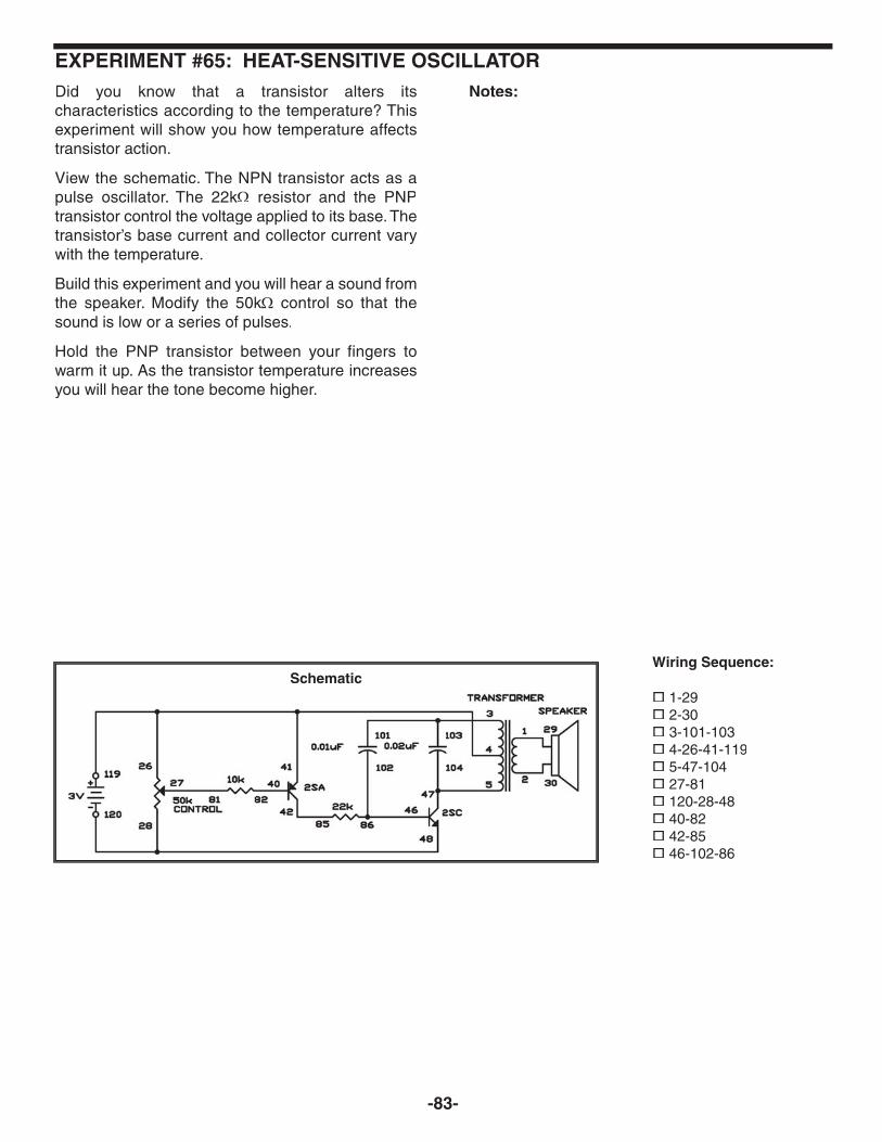
-83-
Did you know that a transistor alters itscharacteristics according to the temperature? Thisexperiment will show you how temperature affectstransistor action.
View the schematic. The NPN transistor acts as apulse oscillator. The 22kΩ resistor and the PNPtransistor control the voltage applied to its base. Thetransistor’s base current and collector current varywith the temperature.
Build this experiment and you will hear a sound fromthe speaker. Modify the 50kΩ control so that thesound is low or a series of pulses.
Hold the PNP transistor between your fingers towarm it up. As the transistor temperature increasesyou will hear the tone become higher.
Notes:
EXPERIMENT #65: HEAT-SENSITIVE OSCILLATOR
SchematicWiring Sequence:
� 1-29� 2-30� 3-101-103� 4-26-41-119� 5-47-104� 27-81� 120-28-48� 40-82� 42-85� 46-102-86

-84-
Now you will let one oscillator control another tocreate an alarm. Here we have a multivibrator-typeoscillator controlling a pulse oscillator. The pulseoscillator produces frequency in the audible range(the range that our ears can hear, about 20 to 20kHertz). The multivibrator circuit on the left side of theschematic should look familiar. The multivibratorcommands the pulse oscillator by allowing current toflow to the transistor base.
Build the experiment and press the key to hear thealarm sound coming from the speaker. You hear thealarm resonate turning on and off as the pulseoscillator turns on and off.
This intermittent sounding alarm is more beneficialthan a continuous tone, because it is morenoticeable. You can experiment with this experimentby varying the values of the 22kΩkk , 47kΩkk , and 100kΩkkresistors, and the 0.02μF capacitor.
Notes:
EXPERIMENT #66: PULSE ALARM
Wiring Sequence:
� 1-29� 2-30� 3-103-109� 4-42-45-138� 5-47-110� 40-113-87� 41-112-75� 43-111-85� 44-114-73-89� 46-104-90� 76-86-88-74-48-124� 119-137� 121-122
Schematic

-85-
In this experiment you will make a push/pull, squarewave oscillator. This oscillator is known a push/pullbecause it uses two transistors that are connectedto each other. They take turns maneuvering so thatwhile one transistor is “pushing,” the other is “pulling.This type of oscillator is called a square waveoscillator because the electrical waveform of thesignal has a square shape.
Slide the switch to position A to turn on the powerafter wiring the circuit. We will be using square wavesignals in later projects therefore, note the soundfrom the speaker.
Notes:
EXPERIMENT #67: PUSHING & PULLING OSCILLATOR
Wiring Sequence:
� 1-29� 2-30� 3-83-101-41� 4-131� 5-81-102-44� 40-82� 45-42-119� 43-84� 120-132
Schematic

-86-
You have seen how a capacitor’s charge/dischargecycle can be used to delay certain circuit operations.Now let’s slow the oscillator action in this project witha 470μF capacitor.
Press and release the key. The circuit oscillates, butslowly shuts down as the capacitor charges up.When the capacitor is fully charged, no current canflow to the oscillator, and it is off. When you press thekey, it instantly discharges the capacitor, and theoscillator resumes working.
On its positive (+) and negative (–) electrodes, adischarged capacitor has an equal number ofelectronics. Electrical charge is stored in a capacitorby drawing electrons from the positive electrode (toactually make it positive) and adding an equalnumber of electrons to the negative electrode (tomake it negative). Charging current or displacementcurrent is the current that flows to charge thecapacitor. The same amount of current must flow inthe opposite direction when the capacitor isdischarging. This current is known as dischargecurrent or displacement current.
With the voltmeter function if you have a VOM, use itto measure the charge on the capacitor. Thedisplacement current can be measured with thecurrent function.
This electrical-storage ability makes capacitorsuseful in many different ways. However, this storageability can be dangerous in very high voltage circuitsdue to possible shock if you are not careful with it.You need to discharge capacitors before touchingthem if they use voltages above 50V.
Notes:
EXPERIMENT #68: SLOW SHUT-OFF OSCILLATOR
Schematic
Wiring Sequence:
� 1-29� 2-30� 3-85-105-109� 4-120� 5-41-110� 40-106-86� 42-118-137� 117-138-119

-87-
This circuit has a multivibrator connected to a pulsetype oscillator. Rather than turning the oscillatorcompletely on and off, the multivibrator provides atremolo effect (a wavering tone).
After you build the circuit, use the control to vary thebase current supplied to the NPN transistor. Thischanges the charge/discharge rate of the 0.1μF and0.05μF capacitors, as well the frequency of the pulseoscillator.
The key works to turn the whole circuit on and off.You can substitute it with the slide switch. Bychanging the 10μF and 3.3μF capacitor values, youcan change the tonal range.
Try using the switch or the key to add additionalcomponents to the circuit (like an extra capacitor inparallel with the 10μF or 3.3μF), so you can alterfrom one tonal range to another, quickly. Thesechanges will make a more complete organ from thisexperiment. Be sure to make notes on what you do.
Notes:
EXPERIMENT #69: ELECTRONIC ORGAN OSCILLATOR
Wiring Sequence:
� 1-29� 2-30� 3-47-106� 4-74-45-42-119� 5-105-109� 27-46-110� 28-86� 40-111-80� 41-114-78� 43-113-82� 44-112-87-76� 77-75-81-79-48-138� 73-85-88� 120-137
Schematic

-88-
VIII. MEET THE OPERATIONAL AMPLIFIER

For this section you will need some basicunderstanding about the operational amplifierintegrated circuit. First, we can use separate powersources or we can use one power source for both thecircuit and the IC.
The operational amplifier (often called “op amp” forshort) can be operated as a non-inverting amplifier,an inverting amplifier, or a differential amplifier. Anon-inverting amplifier reproduces an input signal asan output signal without any alteration in polarity. Aninverting amplifier does the reverse: its output hasthe reverse polarity of its input. The differentialamplifier has an output that is the contrast betweenthe strengths of the two input signals.
Comparing two voltages and telling you which one isstronger than the other is the job of a comparator. Wecall the controlled voltage the reference voltagebecause we use it as a reference for measuring othervoltages. The voltage that is compared is the inputvoltage.
The reference voltage in this experiment is about3.7V. It is connected to terminal 68 of one of the opamp integrated circuit. Input voltage is connected toterminal 69 of the same IC. The LED will light if thisinput voltage is higher than the reference voltage,and the LED stays off if it is lower. The operationalamplifier acts as an inverting amplifier for thereference voltage to keep the LED turned off, or as anon-inverting amplifier to light the LED.
Build the experiment and then set the switch toposition A. This supplies an input of 6V. The LED lightsbecause the input voltage is higher than the referencevoltage. Now slide the switch to position B. Thissupplies an input voltage of 1.5V. The comparator ICdoes not turn on the LED, because the input voltageis now lower than the reference voltage.
Notes:
EXPERIMENT #70: OPERATIONAL AMPLIFIER COMPARATOR
Schematic
-89-
Wiring Sequence:
� 31-67� 84-82-33-70-121� 63-122� 68-83-78� 69-81-76� 75-132� 77-119-124� 120-133� 123-131

After you finish the wiring, set the switch to position B.
LEDs 1 and 2 indicate the output voltage of theoperational amplifier IC. An LED lights if it isconnected to 1.5V or higher. In this experiment, weconnect the two LEDs in series, so they only lightwhen connected with about 3V. When they are off,the output voltage of the operational amplifier mustbe less than 3V.
View the schematic diagram. With the switch atposition B, the 1.5V battery voltage is connected totwo 10kΩkk resistors, with the positive terminal of theoperational amplifier connected between theresistors. These two 10kΩkk resistors divide the 1.5Vsupply voltage in half. This signifies the positive inputterminal receives an input voltage of only 0.75V.
To total the output voltage of the operational amplifieryou multiply its input voltage by the amplificationfactor (R1/R2) + 1. So, the output voltage is 0.75V x((220kΩkk / 100kΩkk ) + 1) = 2.4V.Slide the switch position A. This eliminates the 10kΩkkresistors from the circuit, so the amplifier’s positiveinput terminal receives the full 1.5V input voltage.Using the above equation, you can see that theoutput voltage of the operational amplifier is now1.5V x ((220kΩ / 100kΩ) +1) = 4.8V. Because thevoltage supplied to them is more than 3V, the LEDslight dimly.
Let’s alter the amplification factor. Slide the switch toposition B again and press the key. This adds the47kΩ resistor to the 100kΩ resistor in parallel,making total resistance of R2 about 32kΩkk . Now theoutput voltage is 0.75V x ((220kΩkk / 32kΩkk ) +1) = 5.9V,enough to light the LEDs brightly.
Now slide the switch to position A again (to connect1.5V to the amplifier’s positive (+) input terminal), andpress the key. The LEDs light brightly. Calculating theoutput voltage gives 1.5V x ((220kΩ / 32kΩ) +1) =
11.8V. However, the actual output voltage will belimited by the available battery voltage, which is 1.5V+ 3.0V + 3.0V = 7.5V.
Notes:
EXPERIMENT #71: CHANGING INPUT VOLTAGE
Wiring Sequence:
� 31-67-92� 32-34� 81-89-88-70-36-121� 63-122� 68-90-91-138� 69-132� 82-84-133� 83-131-120� 87-137� 119-124
-90-
Schematic

-91-
In this experiment, you will make a microphoneamplifier, using the operational amplifier (op amp) asa non-inverting amplifier with two power sources. Theearphone acts as a microphone.
Begin by sliding the switch to position B and finishingthe wiring for the circuit. When your wiring is ready,set the switch to position A to turn on the power. Nowrotate the control fully clockwise, and lightly tap your“microphone” – the earphone. The tapping sound isheard through the speaker.The earphone is a better microphone if you removethe end that you put in your ear, by turning it counter-clockwise to unscrew it. To adjust the volume, turnthe control.
As you can observe in the schematic, the operationalamplifier uses two power sources: 4.5V for the circuitand 9V for the IC. The signal from the earphone isconnected to the operational amplifier’s non-invertinginput through the control. The input is amplified, andthe output is applied to the transformer. The gainthrough the amplifier is about 100, determined by theratio R1/R2 (100kΩkk / 1kΩk = 100).
Notes:
EXPERIMENT #72: NON-INVERTING DUAL SUPPLY OP AMP
Wiring Sequence:
� 1-29� 2-30� 3-67-90� 27-69� 63-131� 68-89-75� 70-134� 121-135� 122-132� 124-119-26-76-5-14-EARPHONE� 28-13-EARPHONE
Schematic

-92-
This is another two-power source microphoneamplifier, but this one is an inverting amplifier. Youwill use the earphone as a microphone again.
Slide the switch to position B and construct thecircuit. Once you finish the wiring, slide the switch toposition A to turn the power on, adjust the controlclockwise, and speak into the “microphone” – theearphone. This project works just like the precedingone.
IC 2 is an inverting amplifier and IC 1 is used as abuffer between the earphone and IC2, and has again of 1. IC2 is an inverting amplifier, with the inputapplied through its negative (–) terminal, not thepositive (+) one as in our last project. IC2’s gain isabout 100, as determined by:R1/R2 = 100k/1k=100.
If you increase R1 or decrease R2, the gain becomeslarger. See what occurs to the gain when you alterthe value of R2 to 470.
Notes:
EXPERIMENT #73: INVERTING DUAL SUPPLY OP AMP
Wiring Sequence:
� 1-29� 2-30� 3-64-90� 27-69� 63-131� 65-89-76� 68-67-75� 70-134� 121-135� 122-132� 124-119-26-66-5-14-EARPHONE� 28-13-EARPHONE
Schematic

-93-
In Projects 72 and 73 (“Non-inverting Dual SupplyOp Amp,” and “Inverting Dual Supply Op Amp,”respectively), we used the operational amplifier withtwo power sources. In this experiment, we will makea single-power source, non-inverting microphoneamplifier. Again, the earphone works as amicrophone.
Slide the switch to position B and assemble thecircuit. When you competed the wiring, slide theswitch to position A to turn on the power, alternatethe control clockwise, and speak into themicrophone. The experiment works just like Projects72 and 73, but you’ll notice something different.
The contrast comes from the gain of this microphoneamplifier. It is still determined by R1 and R2, but nowit’s much bigger. Can you observe why? Yes, we usethe 100Ω resistor in place of the 1kΩ resistor fromthe last two experiments. Try changing R2 to 1kΩ,and the gain drops to the level of the lastexperiments.
In this experiment, two power sources are connectedin series to operate the dual operational amplifier at9V. But the operational amplifier can work at half thisvoltage, at 4.5V. See what occurs when youdisconnect the operational amplifier from batteryterminal 122 and connect it to terminal 119.
Notes:
EXPERIMENT #74: NON-INVERTING AMPLIFIER
Wiring Sequence:
� 1-29� 2-30� 3-116� 27-112� 71-114� 81-63-131� 67-90-115� 89-68-113� 84-82-69-111� 119-124� 122-132� 121-26-70-83-72-5-14-EARPHONE� 28-13-EARPHONE
Schematic

-94-
This is the last in the series of microphone amplifiers.Now you will use the operational amplifier as adifferential amplifier. It is a two-power source typeamplifier, and this time we use the speaker as amicrophone.
Slide the switch to position B and construct thecircuit. When you finish the wiring, apply theearphone to your ear, slide the switch to position Ato turn on the power, and tap the speaker lightly withyour finger.
In this circuit the operational amplifier is configuredto amplify the difference between its positive (+) andnegative (–) inputs, so we call it a differentialamplifier. The speaker is connected to thetransformer, which is then connected to theamplifier’s inputs, so the speaker signal will beamplified.
In a speaker, an electrical signal flows through a coiland creates a magnetic field; the magnetic fieldchanges as the electrical signal changes. Themagnetic field is used to move a small magnet, andthis movement creates variations in air pressure,which travel to your ears and are interpreted assound.
This circuit uses the speaker as a microphone. In thisarrangement, your voice creates variations in airpressure, which move the magnet inside thespeaker. The moving magnet’s magnetic field createsan electrical signal across both ends of a coil. Thissmall signal is applied to the primary of thetransformer, which then results in larger signal at thesecondary side of the transformer.
This circuit is simplified by using the speaker as amicrophone. To use the earphone as in previousexperiments, you would have to make a far morecomplex circuit.
Notes:
EXPERIMENT #75: DUAL-SUPPLY DIFFERENTIAL AMPLIFIER
Wiring Sequence:
� 1-29� 2-30� 3-110� 5-68-93� 63-131� 69-81-109� 70-134� 121-135� 122-132� 124-119-82-13-EARPHONE� 94-67-14-EARPHONE
Schematic

-95-
You know that an LED promptly lights when you turnit on. You can also light it up gradually. In this project,you’ll be able to observe the LEDs slowly get brighterwhile you hold down the key.
This circuit arrangement is called a Miller integratingcircuit. The output of the circuit increases as its inputrises. The integrating circuit increases the value ofthe 100μF capacitor above its actual value. Whenyou press the key, the LEDs become brighter and thecapacitor charges slowly through resistor R. Settingthe switch to position B discharges the capacitor, andthe LEDs turn off.
Before completing the project, set the switch toposition B, to discharge the capacitor. Set the switchto position B and hold the key down to watch LEDs1, 2, and 3 become brighter. In about 5 seconds theywill reach maximum brightness. Now set the switchto B to discharge the capacitor, then hold down thekey to do the experiment again.
Notes:
EXPERIMENT #76: MILLER INTEGRATING CIRCUIT
Schematic
Wiring Sequence:
� 31-63-122-137� 32-34� 35-37� 38-72� 71-67-116-133� 68-90-115-132� 69-124-119� 70-121� 89-138

-96-
In this experiment, we will make a constant currentcircuit, using an operational amplifier and atransistor. This circuit maintains a constant currenteven when the input voltage is changed, becausemore energy is used up in the circuit.
View the schematic. When the current is modified,the voltage across R1 is also modified. The output ofthe operational amplifier changes corresponding tothe feedback signal from R1. This output from theamplifier controls the base voltage of transistor Q1allowing it to maintain the continual current.
First set the switch to position A, and press the keywhile monitoring LED 1. When the key is pressed itgets dimmer. This occurs because both LED 1 andLED 2 are in the circuit when the key is closed. Thetotal current through the circuit is the same, but nowit is split between LED 1 and LED 2, so LED 1 getsdimmer.
Set the switch to position B with the key off. Do younotice any changes in LED brightness from positionA to position B? Setting the switch to B modifies thesupply voltage from 9V to 6V. However, the currentremains constant again, so the LED brightness is notaffected.
Notes:
EXPERIMENT #77: STABLE-CURRENT SOURCE
Schematic
Wiring Sequence:
� 31-132-137� 32-35-47� 34-138� 46-67� 48-68-75� 63-131-122� 69-119-124� 76-70-121� 123-133

-97-
Now you’re going to make a blinking LED circuitusing an operational amplifier. In this experiment, anLED continuously lights and turns off slowly.
Slide the switch to position B and connect the wiresfor this circuit. When you finish connecting theproject, slide the switch to position A to turn on thepower. After a couple seconds, you’ll see the LEDstart to blink. Watch carefully and you should be ableto observe that it’s on and off periods are aboutequal.
The operational amplifier works as an astablemultivibrator at low frequency. You can alter theperiod of oscillation (the LED blinking rate) by usingdifferent values for R and C. See what happens tothe blinking rate when you make the value of R220kΩkk .
One last thing - the operational amplifier has highinput resistance at its inputs - so there is very littlecurrent flowing into its inputs. This means you canoperate it to build accurate blinkers and timers withlonger intervals.
Notes:
EXPERIMENT #78: OPERATIONAL AMPLIFIER BLINKING LED
Schematic
Wiring Sequence:
� 81-31-63-131� 33-67-90-94� 93-68-113� 69-82-84-89� 83-70-114-121� 119-124� 122-132

-98-
Begin by sliding the switch to position B and wiringthe circuit. This LED flasher uses two diodes. As youbuild this experiment, be sure to connect thesediodes in the correct direction.
When you finish assembling the experiment, turn onthe power by sliding the switch to position A, andpress the key. The LED starts blinking immediately.Even if you don’t press the key, this LED flasherstarts flashing shortly after you turn on the power; ifyou press the key, it begins blinking right away.
This LED flasher uses an operational amplifier as anastable multivibrator, but its flashing time is muchshorter because of the two diodes.
Notes:
EXPERIMENT #79: LED FLASHER
Schematic
Wiring Sequence:
� 81-31-63-131-138� 33-67-88-90-76� 68-115-137-128-125� 69-87-82-84� 83-70-116-121� 75-127� 89-126� 119-124� 122-132

-99-
The LED circuits in experiments 78 and 79(“Operational Amplifier Blinking LED” and “LEDFlasher”) each use one LED, but the circuit in thisproject uses two LEDs that take turns lighting. Slidethe switch to position B and assemble the circuit.Then, turn the power on by sliding the switch toposition A and wait for a few seconds. The LEDs lightand turn off in rotation.
The operational amplifier works as an astablemultivibrator. When the output is low, LED 2 lights;when it is high, LED 1 lights.
You can alter the speed of the blinking by usingdifferent values for R and C. See how the speed ofthe pulses alters when you alter the value of R to220kΩkk .
Notes:
EXPERIMENT #80: DOUBLE LED BLINKER
Schematic
Wiring Sequence:
� 31-36-67-90-94� 33-70-135� 34-63-132� 93-68-113� 81-89-69� 82-114-124-119� 121-134� 122-131

-100-
You’ve built many circuits using the operationalamplifier, but there are lots of other ways to use thishandy IC. One of them is the single flashmultivibrator. With this multivibrator, you can makethe LED stay on for a preset amount of time whenthe key is pressed - a single flash light.
Slide the switch to position B and construct thecircuit. Turn the power on by sliding the switch toposition A. The LED lights, but quickly turns off. Now,press the key and observe what happens. The LEDlights and stays on for 2 to 3 seconds and then turnsoff.
By using different values for C You can change theamount of time the LED is on. Change the value ofC from 10μF to 100μF and see what occurs to theLED. It stays on longer.
Notes:
EXPERIMENT #81: SINGLE FLASH LIGHT
Schematic
Wiring Sequence:
� 31-63-94-131-138� 33-67-114� 85-68-110� 69-82-89-93� 70-134� 81-86-130-124-119� 90-115� 109-137-129� 113-116� 121-135� 122-132

-101-
Now you are going to use the operational amplifieras a comparator and as a Schmitt trigger circuit. Aslong as its input voltage exceeds a certain value, theoperational amplifier will produce a signal. View theschematic: can you see how it works? The inputlevel that turns on the output is higher than the levelthan turns it off. So once a Schmitt trigger circuitturns on, it stays on unless the input dropssignificantly. We call this type of operation a“hysteresis loop.”
Build the circuit, but don’t press the key yet. Theoperational amplifier serves as a comparator in thisstate. When you alternate the control, LEDs 1 and 2take turns lighting at some point. Note that this pointdoesn’t alter whether you turn the control clockwiseor counterclockwise.
Now push the key and you have a Schmitt triggercircuit, which makes a hysteresis loop. Turn thecontrol and see how the circuit operation is differentfrom before.
As the ratio of resistors RB/RA increases, the widthof hysteresis becomes narrower. Try using differentvalues for RA and RB, and notice how the widthchanges.
Notes:
EXPERIMENT #82: INTRODUCING THE SCHMITT TRIGGER
Wiring Sequence:
� 70-36-26-121� 27-83� 63-28-130-131� 34-33-67-90� 68-134� 84-69-138� 89-137� 119-124-135� 122-132� 31-129
Schematic

-102-
The digital LED can’t display all 26 letters of thealphabet, but it’s possible to exhibit many of them.Let’s make an LED display that intersperse showsthe initials E and P of our ELECTRONICPLAYGROUND. You can show other initials too.
Slide the switch to position B and construct thecircuit. Once you have completed the wiring, slide theswitch to position A to turn on the power, and you’llobserve the letters E and P lighting alternately on theLED display.
IC 1 works as an astable multivibrator and exhibitsthe letter E. IC 2 is used as an inverter, with an outputthat is opposite to that of IC 1; it displays the letter P.
Now that you’ve successfully displayed the letters Eand P, why not try showing other letters? It should beeasy if you take a close look at the schematic.
Notes:
EXPERIMENT #83: INITIALS ON LED DISPLAY
Schematic
Wiring Sequence:
� 22-17-18-19-63-131-81� 20-65-67-90-94� 21-64� 83-114-70-25-121� 66-69-82-84-89� 93-68-113� 119-124� 122-132

-103-
You know that digital circuits produce low or high (Lor H) outputs (0 or 1). Now you’re going to create alogic tester that shows 1 for high level (H) and 0 forlow level (L) on the LED display.
Slide the switch to position B and construct thecircuit. When you finish the wiring, slide the switch toposition A to turn on the power. The number 0 is onthe display because the test terminal (terminal 13) isat low level when no input is exerted. Attach the testterminal-to-terminal 122 to apply +4.5V. The displayalters to 1.
View the schematic. The operational amplifier worksas a comparator. The 22kΩ and 10kΩ resistorsproduce a reference voltage of 3V at its negative (-)input terminal. When the voltage at its positive (+)terminal exceeds this reference voltage, thecomparator’s output level goes high, turning offtransistor Q1. Now segments A, D, E, and F on thedisplay turn off, leaving a 1 on the display.
Notes:
EXPERIMENT #84: LOGIC TESTING CIRCUIT
Wiring Sequence:
� 17-18-19-20-44� 86-79-63-21-23-45-132� 43-80-82� 67-81� 68-83-85� 119-124� 122-131� 69-89-13-CHECK POINT� 121-25-70-90-84-14-CHECK POINT
Schematic
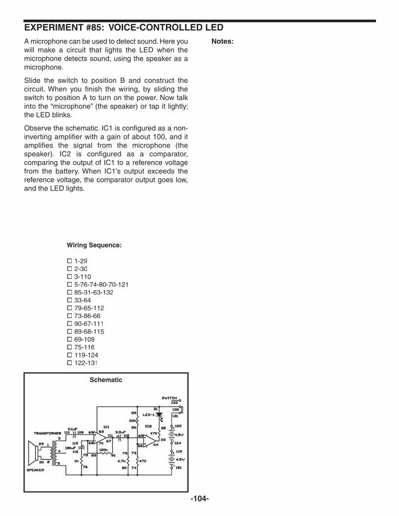
-104-
A microphone can be used to detect sound. Here youwill make a circuit that lights the LED when themicrophone detects sound, using the speaker as amicrophone.
Slide the switch to position B and construct thecircuit. When you finish the wiring, by sliding theswitch to position A to turn on the power. Now talkinto the “microphone” (the speaker) or tap it lightly;the LED blinks.
Observe the schematic. IC1 is configured as a non-inverting amplifier with a gain of about 100, and itamplifies the signal from the microphone (thespeaker). IC2 is configured as a comparator,comparing the output of IC1 to a reference voltagefrom the battery. When IC1’s output exceeds thereference voltage, the comparator output goes low,and the LED lights.
Notes:
EXPERIMENT #85: VOICE-CONTROLLED LED
Schematic
Wiring Sequence:
� 1-29� 2-30� 3-110� 5-76-74-80-70-121� 85-31-63-132� 33-64� 79-65-112� 73-86-66� 90-67-111� 89-68-115� 69-109� 75-116� 119-124� 122-131

-105-
The operational amplifier (op amp) works well as anoscillator. In this experiment, you will build an electricbuzzer that makes a continuous beep. By rotating thecontrol you can change the tone of this buzzer.
When you finish the wiring, set the control to the 12o’clock position and press the key. From the speakeryou hear a continuous beep. Turn the control as youpress the key; the tone of the buzzer changes.The electronic buzzer only makes a beep, but it canbe used for many different purposes, as you’ll seelater.
This circuit is an astable multivibrator working as anoscillator to produce a square wave signal for thespeaker. Adjusting the control changes thefrequency, so the tone of the sound is different. Thefrequency is determined by the resistors andcapacitor connected to the input terminals of theoperational amplifier. Try changing the capacitor to0.02μF or 0.1μF and see how the tone changes.
Notes:
EXPERIMENT #86: BUZZIN’ WITH THE OP AMP
Schematic
Wiring Sequence:
� 1-29� 2-30� 3-116� 5-84-70-106-121� 63-27-138� 28-81� 67-90-92-115� 91-68-105� 69-82-83-89� 119-124� 122-137

-106-
The electronic buzzer we built in the previous circuitcan only make a continuous beep, but we can makea similar circuit that produces various siren sounds.Your going to make a siren that gives out a soundwith a variable pitch. When you move the switch, thissiren wails and then creates a continuous high-pitched noise.
Slide the switch to position B and assemble thecircuit. When you complete the wiring, turn the poweron by sliding the switch to position A. You hear thespeaker produce a sudden, roaring siren sound. Atfirst the sound is low and becomes higher, thenchanges to a steady tone in about 3 to 4 seconds.When you press the key and release it, the capacitordischarges and starts the siren sound again.
You can understand how this works by looking at theschematic. The pitch changes as the 10μF capacitoris charged through the 100kΩ resistor. IC 2 is anastable multivibrator. IC 1 is a buffer between thecapacitor and IC 2.
Notes:
EXPERIMENT #87: SWEEP OSCILLATOR
Wiring Sequence:
� 1-29� 2-30� 3-116� 5-84-70-106-114-137-121� 89-63-131� 64-88-92-115� 65-87-105� 66-82-83-91� 68-67-81� 90-69-113-138� 119-124� 122-132
Schematic

-107-
Here’s another siren that alters its pitch. The siren webuilt in our last experiment alters pitch from low tohigh, but this one alters its pitch from high to low andfinally stops making any sound. When it stops, pressthe key and the siren sound will start again.
Set the switch to position B and put together thecircuit. When you finish the wiring, slide the switch toposition A to turn on the power. You hear a high-pitched siren sound that becomes progressivelylower, it sounds like a falling bomb. Press the key tostart the sound again.
Like the siren in our last experiment, this siren usesIC 1 as a buffer and IC 2 as an astable multivibrator.The capacitor C and the resistor R change the pitchof the siren sound. The pitch adjusts slowly when youincrease the values of C and R, and adjusts quicklywhen you decrease their values. Try using the 3.3μFcapacitor for C and notice how the pitch changes.
Notes:
EXPERIMENT #88: FALLING BOMB
Wiring Sequence:
� 1-29� 2-30� 3-116� 5-84-94-106-70-121� 63-113-131-138� 64-90-92-115� 65-105-89� 66-82-83-91� 68-67-81� 93-69-114-137� 119-124� 122-132
Schematic

-108-
The sirens in Projects 88 and 89 (“Sweep Oscillator”and “Falling Bomb”, respectively) adjust the pitchonly in one direction. This circuit makes a low soundthat becomes higher, and goes back to its originallow sound. The siren sounds only when you pressthe key.
Set the switch to position B and build the circuit. Turnon the siren by sliding the switch to position A. Whenyou press the key, the siren starts over at the originallow pitch. Do you hear the siren sound change pitch?Does it do so as you expected? IC 1 is an oscillatorthat produces a triangular signal when you press thekey. Then the output is sent to IC 2, which acts as anastable multivibrator.
See how the pitch changes when you set C to0.02μF and then to 0.1μF.
Notes:
EXPERIMENT #89: ALERT SIREN
Wiring Sequence:
� 1-29� 2-30� 3-116� 5-70-108-137-121� 80-63-132� 64-90-92-115� 65-89-107� 66-82-91� 81-67-118� 78-79-68-117� 69-119-124� 77-138� 122-131
Schematic

-109-
This siren gives off alternating high and low sounds.Slide the switch to position B and construct thecircuit. After you complete the wiring and slide theswitch to position A, the power turns on and thespeaker creates the sound of a two-pitch siren.
This siren is made up of two astable multivibrators.IC 2 provides the normal beep sound. IC 1 producesthe signal that alters the pitch of its sound at regularintervals.
Let’s execute a small experiment now. The sirengives out an intermittent beep instead of the two-pitch sound once you detach the 22kΩk resistor. Canyou decipher why? The IC 1 interrupts the sirensound produced by IC 2.
Notes:
EXPERIMENT #90: CRISIS SIREN
Wiring Sequence:
� 1-29� 2-30� 3-116� 5-83-70-108-112-121� 85-63-131� 64-90-92-115� 65-107-89� 66-82-84-86-91� 81-94-88-67� 93-68-111� 69-80-87� 79-119-124� 122-132
Schematic

-110-
This is the operational amplifier version of theelectronic metronome from Project 3 (“ElectronicMetronome”). Slide the switch to position B, andconnect the wires carefully - this project is moreintricate than most of the others. When you completeassembling the circuit, set the control to the 12o’clock position, and slide the switch to position A toturn on the power. You’ll hear a pip noise from thespeaker at fixed intervals. Now gradually rotate thecontrol clockwise, and the beats come faster.
Now observe the schematic. IC 1 and IC 2 are usedas astable multivibrators, as in our last experiment.But you’ll notice that IC 1 uses diodes to generateshort pulses and the control is used to modify thespeed of the pulses. The transistor turns on eachtime a pulse is generated, and creates a sound.
Notes:
EXPERIMENT #91: OP AMP METRONOME
Wiring Sequence:
� 1-29� 2-30� 3-114� 5-47� 27-127� 28-77� 46-80-84� 79-70-108-116-48-121� 63-131� 89-91-113-64� 65-90-107� 86-92-66� 78-76-83-88-67� 68-115-125-128� 82-87-69� 75-126� 85-81-119-124� 122-132
Schematic

-111-
This burglar alarm makes a buzzing sound whenanyone sneaking into your house trips over a wireand breaks it off or disconnects it from a terminal. Tryto figure out how to connect a switch to the door ofyour house, so that the alarm sounds when a burglaropens the door, instead of stretching out the wire.
Start by sliding the switch to position B andassembling the circuit. When you complete thewiring, connect the terminals 13 and 14 to the longwire, and slide the switch to position A to turn on thepower. No sound comes from the speaker, at thistime.
Detach the wire from terminal 13,to test the alarm.The speaker gives out a beep. This beep is the alarmthat tells you a burglar is about the break into yourhouse.
As you can observe in the schematic, this burglaralarm uses the operational amplifier as an astablemultivibrator, as the electronic buzzer in the lastexperiment did. You can change its frequency byusing different values for the 10kΩkk resistor and the0.1μF capacitor. Note how the tone of the buzzeralters when you set the 10kΩ resistor to 47kΩ orswitch the 100kΩ and 220kΩ resistors with eachother.
Notes:
EXPERIMENT #92: BURGLAR BUZZER
Schematic
Wiring Sequence:
� 1-29� 2-30� 3-114� 5-14-83-70-110-121� 13-89-68109� 81-63-132� 67-90-92-113� 69-82-84-91� 119-124� 122-131� 13-14 (LONG WIRE)

Do you sleep late? Even if you do, don’t fear!Because you can make the siren in this circuit alarmso that wakes you up gradually as the day dawns.Set the switch to position B, construct the circuit, thenset the switch to position A to turn it on. You shouldhear sound from the speaker.
When you expose the CdS cell to light, the sirensounds. The siren sound stops when you cover theCdS. The alarm siren is made with a multivibrator,and controls its operation with the CdS.
When you go to bed at night and sleep with yourroom dark, turn on this circuit. The next morning, thealarm siren will wake you up.
Notes:
EXPERIMENT #93: GET UP SIREN
-112-
Schematic
Wiring Sequence:
� 1-29� 2-30� 3-116� 5-83-108-70-121� 15-63-132� 16-81� 67-90-92-115� 91-68-107� 69-82-84-89� 119-124� 122-131
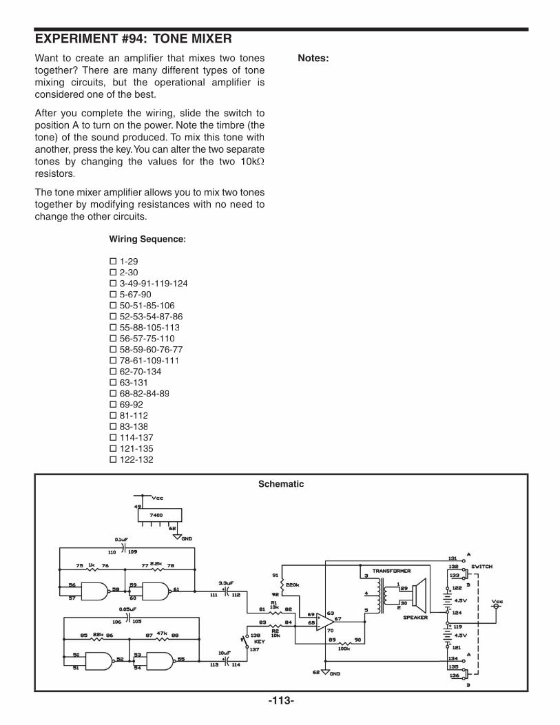
-113-
Want to create an amplifier that mixes two tonestogether? There are many different types of tonemixing circuits, but the operational amplifier isconsidered one of the best.
After you complete the wiring, slide the switch toposition A to turn on the power. Note the timbre (thetone) of the sound produced. To mix this tone withanother, press the key. You can alter the two separatetones by changing the values for the two 10kΩresistors.
The tone mixer amplifier allows you to mix two tonestogether by modifying resistances with no need tochange the other circuits.
Notes:
EXPERIMENT #94: TONE MIXER
Wiring Sequence:
� 1-29� 2-30� 3-49-91-119-124� 5-67-90� 50-51-85-106� 52-53-54-87-86� 55-88-105-113� 56-57-75-110� 58-59-60-76-77� 78-61-109-111� 62-70-134� 63-131� 68-82-84-89� 69-92� 81-112� 83-138� 114-137� 121-135� 122-132
Schematic

-114-
Now you are going to produce a loud sound bycombining an operational amplifier with twotransistors. After you finish the wiring, set the switchto position A to turn on the power. You hear a loudsound from the speaker when you press the key.
A capacitor-resistor oscillator is the signal source forthis sound. The operational amplifier acts as aninverting amplifier, and transistors Q2 and Q3 causethe speaker to create the sound. This circuit is calleda single ended push-pull circuit (SEPP). You havelearned about push-pull circuits. Single endedsignifies that the circuit has only one output. Mostamplifiers have a second output that is connected tothe negative (–) side of the battery.
Notes:
EXPERIMENT #95: OP AMP POWER AMPLIFIER
Wiring Sequence:
� 1-29� 2-30� 3-90-67-47-44� 5-94-48-119-124� 73-81-86-87-32-113-45-131� 33-63-43� 35-46-70� 76-92-36-134� 91-88-104-40� 75-100-111-41� 74-114-42� 68-80-89� 69-93� 79-138� 82-84� 83-102-103� 85-99-101� 112-137� 121-135� 122-132
Schematic

-115-
VCO? What’s that? VCO stands for voltagecontrolled oscillator, and as the name implies, thisoscillator changes its oscillation frequency accordingto the voltage applied to the circuit. The circuitcreates two different output signals that havetriangular and square waves.
When you finish the wiring sequence, slide the switchto position A to turn on the power. Turn the controlslowly while you listen to the sound from theearphone. The sound becomes lower when you turnthe control clockwise.
Turning the control changes the voltage at terminal27, which changes the 0.01μF capacitor’s chargingand discharging times, which changes the oscillatorfrequency. The output signal from the first operationalamplifier is a triangular wave signal is at terminal 67,and is applied to terminal 65 of the second amplifier.The second amplifier acts as a comparator, andproduces a square wave signal at terminal 64.
Notes:
EXPERIMENT #96: VCO
Wiring Sequence:
� 79-63-26-131� 27-87-89� 46-91� 47-76� 86-92-109-64� 65-78� 66-80-83-85� 67-102-77� 68-90-101-75� 69-88-81� 84-70-134� 121-135� 122-132� 124-119-28-48-94-82-14-EARPHONE� 110-93-13-EARPHONE
Schematic

-116-
IX. MORE FUN WITH OPERATIONAL AMPLIFIERS

-117-
In this experiment, you will create a voice input powermeter. The brightness of the LED in this circuitchanges according to the level of voice input thatcomes from the microphone (the earphone). Sincevoice levels change quickly, the brightness of the LEDshould also adjust quickly. In order to show thehighest voice input levels, we use a circuit called apeak-level hold circuit. This allows the LED to holdcertain brightness after it reaches peak strength,rather than turning off immediately.
Build the circuit, and set the switch to position A. Youwill use the earphone as a microphone. Speak loudlyor blow strongly into the earphone. You can see theLED get brighter temporarily and then gradually growdimmer.
Study the schematic. You can see that the signal fromthe earphone travels through the PNP transistor andthen becomes the positive (+) input for the firstoperational amplifier. The output level of the firstoperational amplifier is stored in the 100mF capacitor,and slowly discharges through the 47kΩkk resistor. TheLED gets dim as the voltage on the capacitordecreases. The voltage that lights the LED is also fedback to the negative (-) input of the first operationalamplifier, where it is compared to the signal from theearphone. If the signal from the earphone is larger, itcharges the 100mF capacitor; otherwise there is nooutput from it.
You can modify the brightness of the LED bychanging resistor RA (47kΩ) or the capacitor CA(100μF).
Notes:
EXPERIMENT #97: VOICE POWER METER
Wiring Sequence:
� 112-13-EARPHONE� 119-124-116-33-88-90-80-72-14-EARPHONE� 31-65-64-82� 32-71� 93-111-40� 79-94-113-41� 63-42-131� 87-66-127-115� 67-129-128� 81-68-130� 89-69-114� 70-134� 121-135� 122-132
Schematic

-118-
Do you know what a reset circuit does? It activatesother circuits and detects any power fluctuations inorder to prevent malfunctions. In this experiment, wechange the supply voltage to the circuit with theswitch. The power to the display portion of the circuitis on, or logic high, when the switch is set to positionA; it is off when the switch is at position B. When thecircuit has been reset the LED display shows 1.
Let’s start experimenting. First, finish the wiring andset the switch to position B. Now, with the switch setto B, the power reset circuit operates under 6V, andthe three LEDs light dimly. The LED display is off,meaning that the display circuit is not activated.
Now set the switch to position A. You can see thethree LEDs light brightly because the supply voltagehas been modified to 9V. For a moment, the LEDdisplay still shows no change, indicating that thecircuit is being reset. After a short interval, the LEDdisplays 1 to show that the circuit has finishedresetting and now it is stabilized.
Set the switch to position B to switch the power backto 6V. You will observe the 1 on the LED disappear,because now the display circuit is off.
Study the schematic to understand how the circuitworks. The operational amplifier is a comparator. The3 LEDs are connected together to make a referencevoltage of about 5.4V for the negative (–) terminal.With the switch in position B, the positive (+) terminalreceives about 4.1V, so the comparator does not
allow the display to light. With the switch in positionA, the battery voltage is increased to 9V, and the100μF capacitor gradually causes the comparator’spositive (+) terminal voltage to increase to about 6V.When this voltage exceeds the reference voltage of5.4V, the LED display lights 1.When you set the switch to B, the voltage at theamplifier’s positive (+) terminal discharges throughthe diode, so the voltage is reduced to 4.1V.
Although this circuit seems very simple (consistingof only one operational amplifier), it is very complexand important for later use.
Notes:
EXPERIMENT #98: RESET CIRCUIT
Wiring Sequence:
� 21-23-67-116� 85-70-38-25-121� 31-68-74� 32-34� 35-37� 73-81-63-129-132� 86-82-69-115-130� 119-124� 122-131� 123-133
Schematic
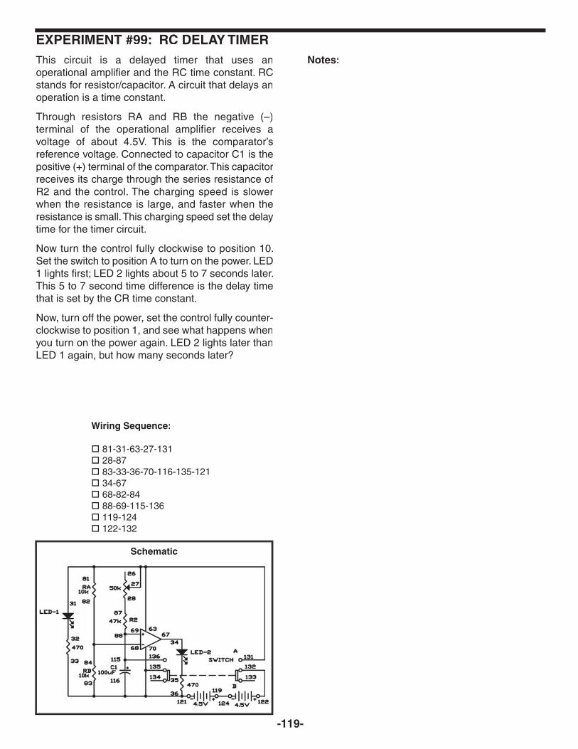
-119-
This circuit is a delayed timer that uses anoperational amplifier and the RC time constant. RCstands for resistor/capacitor. A circuit that delays anoperation is a time constant.
Through resistors RA and RB the negative (–)terminal of the operational amplifier receives avoltage of about 4.5V. This is the comparator’sreference voltage. Connected to capacitor C1 is thepositive (+) terminal of the comparator. This capacitorreceives its charge through the series resistance ofR2 and the control. The charging speed is slowerwhen the resistance is large, and faster when theresistance is small. This charging speed set the delaytime for the timer circuit.
Now turn the control fully clockwise to position 10.Set the switch to position A to turn on the power. LED1 lights first; LED 2 lights about 5 to 7 seconds later.This 5 to 7 second time difference is the delay timethat is set by the CR time constant.
Now, turn off the power, set the control fully counter-clockwise to position 1, and see what happens whenyou turn on the power again. LED 2 lights later thanLED 1 again, but how many seconds later?
Notes:
EXPERIMENT #99: RC DELAY TIMER
Schematic
Wiring Sequence:
� 81-31-63-27-131� 28-87� 83-33-36-70-116-135-121� 34-67� 68-82-84� 88-69-115-136� 119-124� 122-132

-120-
The circuit in this experiment allows you to hearalternating current. You probably know that theelectric power running through your home is analternating current. All your appliances that receivepower from electric outlets operate on AC- includinglamps. Lamps actually flicker at the rate of 60 timesper second, but it looks constant because our eyessee after images. In this experiment you will hearsound converted from light.
Ready to start? After constructing this circuit, turn onthe power to your kit by setting the switch to A. Placethe CdS cell near an electric lamp. Do you hear ahissing sound coming from the earphone? This is thesound of the alternating current. Now place the CdScell under a fluorescent lamp, and listen for a similarsound.
This circuit greatly intensifies the signals of light onthe CdS cell through the operational amplifier. Adjustthe quantity of light on the CdS cell with your hand.You can probably hear the volume of the hissingsound reduce and the quality of the sound improve.See what occurs when you expose the CdS tosunlight.
Notes:
EXPERIMENT #100: LISTEN TO ALTERNATING CURRENT
Schematic
Wiring Sequence:
� 15-88-113� 87-63-131� 76-93-68� 70-121� 69-90� 75-99-114� 122-132� 67-94-81-13-EARPHONE� 124-119-16-100-89-82-14-EARPHONE

-121-
This is a pulse frequency multiplier with onetransistor. It doubles the frequency of the input signal,so it is also called a pulse frequency doubler.
The operational amplifier IC acts as a square-waveoscillator. The output from the oscillator is an ACsignal of about 500Hz.
When you finish the wiring, set the switch to positionA to turn on the power. Connect the earphone toterminals 93 and 134 and press the key to listen tothe oscillating sound of 500Hz. Note the pitch of thetone.
Now, connect the earphone to terminals 13 and 14and press the key. Listen through the earphone; thistime you hear a sound that is an octave higher thanthe previous sound. This means the frequency isdoubled to 1,000Hz.
How does this work? The operational amplifier isconfigured as an oscillator. Transistor Q1 receives asignal from the operational amplifier through thetransistor’s base; the base voltage changes with theoscillations. This result is that opposite phase signalsappear at the transistor’s collector and emitter - whenone signal is at a wave maximum, the other is at thewave minimum. The two outputs from transistor Q1are applied to diodes Da and Db. The diodes passthrough only the positive portion of the waves, sothese two signals combine together to produce adoubled frequency.
Notes:
EXPERIMENT #101: PULSE FREQUENCY MULTIPLIER
Wiring Sequence:
� 125-127-91-13-EARPHONE� 134-110-92-80-83-76-14-EARPHONE� 32-63-87-131� 33-47-107� 35-48-105� 89-36-70-121� 88-90-103-46� 81-86-67-137� 85-68-109� 69-82-84� 75-77� 78-106-128� 79-108-126� 94-104-138� 119-124-135� 122-132
Schematic

-122-
White noise is a noise that has a wide frequencyrange. One kind of white noise is the static noise youhear when you tune your FM radio to an area withno station. When you play electronic musicalinstruments, you can use white noise, a normallyuseless noise, as a sound source.
When you complete building this circuit, set theswitch to position A to turn on the power. Look at theschematic. You will use the noise that is generatedwhen you apply a reverse voltage to the base andthe emitter of transistor Q1.
IC 1 acts as an oscillator. The output of this oscillatoris rectified by diodes D1 and D2, and flows to Q1. IC2 amplifies the noise so that you can hear it throughthe earphone.
Notes:
EXPERIMENT #102: WHITE NOISE MAKER
Wiring Sequence:
� 64-90-13-EARPHONE� 121-114-112-46-47-70-96-84-85-14-EARPHONE� 93-48-101� 94-111-127� 82-88-63-132-126� 76-89-65� 113-66-81-83� 77-91-67-110� 68-95-92� 69-80-87-86� 78-79� 109-128-125� 119-124� 122-131� 102-75
Schematic

-123-
This circuit changes the intervals between eachsound according to the amount of light falling on theCdS cell. The sound changes continuously as youalter the light intensity.
Build the circuit, and set the switch to position A toturn on the power. The speaker makes a sound. Tochange the sound, move your hand over the CdS.
You can calculate the approximate value of thefrequency of the signal by using the equation 1/2 xC1 x R1. However, R1, in this project, is the CdS andis not constant. By changing C1 you can change thevalue of the output frequency. In this experiment,another operational amplifier is used as a buffer, sothe light-controlled sound part of the circuit is notaffected by the speaker sound.
Notes:
EXPERIMENT #103: LIGHT-CONTROLLED SOUND
Wiring Sequence:
� 1-29� 2-30� 3-64-65� 5-86-110-119-124� 15-68-109� 16-66-67-88� 63-131� 69-87-85� 70-134� 121-135� 122-132
Schematic

-124-
Here’s a DC-DC converter circuit; it can make 5VDCfrom 3VDC. Assemble the experiment, set the switchto position A, and see how this circuit works.
The schematic shows how it works. IC 1 is anoscillator; its output controls transistor Q1. Self-induction of the transformer coil generates a highvoltage current. Diode D1 rectifies this voltage andpasses on a high DC voltage current. IC 2 is acomparator that examines the voltage. When theinput voltage to IC 2 is more than 5V, the LED lights.
How does turning the control affect the circuit? Thecontrol is used as a fixed resistor of 50kΩk , so turningthe control has no effect.
Notes:
EXPERIMENT #104 DC-DC CONVERTER
Wiring Sequence:
� 3-134� 5-47-130� 26-67-72-81� 28-69-90-92-94� 31-64� 33-76-83-86-93-91-70-106-116-48-120� 46-71-75� 89-88-63-131� 84-87-65� 85-66-115-129� 82-68-105� 119-124-135� 122-132
Schematic

-125-
This circuit produces light and sound when it detectsyour voice or any other sound. The earphone acts asa microphone. IC 1 amplifies sounds picked up by themicrophone. Diodes Da and Db rectify the amplifiedsignal - that is, they convert the sound signal from ACto DC. The signal travels through IC 2, thecomparator, and activates the LED and the speaker.
When you complete the circuit, rotate the control fullycounter-clockwise, and set the switch to position A.Then rotate the control clockwise while speaking intothe microphone, and set the control in a positionwhere the LED only lights when you speak into themicrophone. Stop speaking and the LED turns off.
Now disconnect the wire between 57 and 62, andreconnect it between 57 and 32. See what happensto the speaker and LED when you blow into themicrophone (earphone).
Notes:
EXPERIMENT #105: SUPER SOUND ALARM
Wiring Sequence:
� 75-63-28-131� 29-76� 30-47� 31-64� 46-86� 56-77-110� 58-59-60-79-78� 85-80-61-109� 66-83� 67-90-73� 68-89-71� 87-69-113� 74-111� 84-91-115-127� 112-129-128� 49-50-51-53-54-135� 114-13-EARPHONE� 122-132� 27-65� 57-26-121-130-48-116-70-92-88-62-33-72-14-EARPHONE� 119-124-134
Schematic
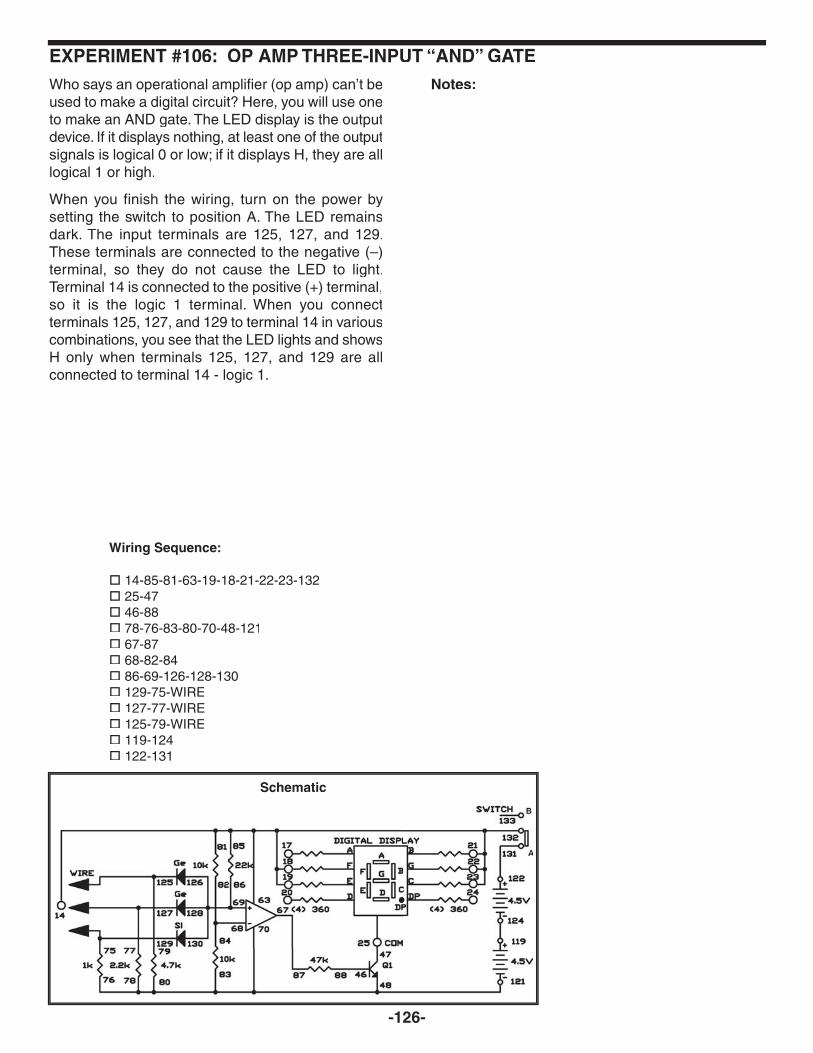
-126-
Who says an operational amplifier (op amp) can’t beused to make a digital circuit? Here, you will use oneto make an AND gate. The LED display is the outputdevice. If it displays nothing, at least one of the outputsignals is logical 0 or low; if it displays H, they are alllogical 1 or high.
When you finish the wiring, turn on the power bysetting the switch to position A. The LED remainsdark. The input terminals are 125, 127, and 129.These terminals are connected to the negative (–)terminal, so they do not cause the LED to light.Terminal 14 is connected to the positive (+) terminal,so it is the logic 1 terminal. When you connectterminals 125, 127, and 129 to terminal 14 in variouscombinations, you see that the LED lights and showsH only when terminals 125, 127, and 129 are allconnected to terminal 14 - logic 1.
Notes:
EXPERIMENT #106: OP AMP THREE-INPUT “AND” GATE
Wiring Sequence:
� 14-85-81-63-19-18-21-22-23-132� 25-47� 46-88� 78-76-83-80-70-48-121� 67-87� 68-82-84� 86-69-126-128-130� 129-75-WIRE� 127-77-WIRE� 125-79-WIRE� 119-124� 122-131
Schematic

-127-
Here’s a timer you can use for taking timed tests orsimply for knowing when an amount of time haspassed. You can preset this timer for up toapproximately 15 minutes. When the time is up, itgives out a continuous buzzer sound until you turnoff the power or press the key to reset the circuit.
After you build this experiment, set the control toposition 2 on the dial and slide the switch to positionA to turn on the power. Hold a stopwatch and start itwhen you press the key. The timer makes a buzzingsound in about 30 or more seconds.
Set the control to each division on the dial from 2 to8, and note how long it takes the timer to produce asound. Setting the timer’s calibration - the time thatpasses at each setting of the dial - requires a lot ofpatience, but it is necessary for making sure yourtimer works accurately. After you set the calibration,you need to make a graph showing each controlposition and the time it takes for the buzzer to sound.Then your tester is ready for use.
Scan the schematic. The control changes thereference voltage of the comparator (IC 1). Theresistor R and the capacitor C determine the timersetting. When the voltage applied to the positive (+)terminal of IC 1 exceeds the reference voltage, thealarm sounds.
The operational amplifier has high input impedance(input resistance), so its current loss is very small,and you can use it to make a timer with a very longsetting. IC 2 works as an astable mulitivibrator thatproduces the buzzer sound.
Notes:
EXPERIMENT #107: TIMER
Wiring Sequence:
� 1-29� 2-30� 3-114� 5-83-70-106-118-137-26-121� 93-63-28-132� 92-90-64-113� 65-105-91� 66-82-84-89� 67-81� 94-69-117-138� 119-124� 122-131
Schematic

-128-
Wouldn’t you like to make a kitchen timer that you canuse for cooking meals? This circuit gives out a buzzersound for 1 to 2 seconds and automatically stops.
Slide the switch to position B, build the circuit, and setthe switch to position A to turn it on. Set the controlto position 2 on the dial, and press the key to start thetimer. After about 40 seconds, the timer sounds for 1to 2 seconds and stops. Use the graph you made inproject 107 to preset this timer.
Look at the schematic. When the preset time is up,the comparator (IC 2) sends out an output. After atime lag of 1 to 2 seconds produced by R and C, thetransistor Q1 turns on to stop the multivibrator. Thesilicon diode discharges C and restores the circuit tothe original state when the timer is restarted.
Notes:
EXPERIMENT #108: COOKING TIMER
Wiring Sequence:
� 1-29� 2-30� 3-114� 5-83-70-104-116-118-137-48-26-121� 27-68� 93-63-28-131� 46-85� 91-103-65-47� 92-88-64-113� 81-84-87-66� 67-82-89� 69-94-117-138-129� 86-90-115-130� 119-124� 122-132
Schematic

-129-
X. RADIO AND COMMUNICATION CIRCUITS

-130-
In emergency situations when there is no power, agermanium diode radio can be used. Generally theydo not perform well and limited to using and crystalearphone since they have no power source.
In this circuit, we will use an operational amplifier soyou can hear the radio through the speaker. Thissimple IC radio uses the dual operational amplifier asa two-power source, non-inverting amplifier.
Slide the switch to position B and assemble theexperiment. After wiring the circuits put up theantenna and connect it to the circuit. Set the controlto the 12 o’clock position and slide the switch toposition A to turn on the power. Turn the tuningcapacitor until you hear a station. You can try pickingup weaker stations, by using the earphone in place ofthe speaker in connections to terminals 1 and 2.
Notes:
EXPERIMENT #109: OPERATIONAL AMPLIFIER AM RADIO
Wiring Sequence:
� 1-29� 2-30� 3-67-90� 5-8-11-76-92-26-119-124� 6-126� 7-12-ANT� 27-69� 28-109� 63-135� 68-89-75� 70-132� 91-110-125� 121-131� 122-134
Schematic

-131-
This circuit is a simplified but effective code transmittersimilar the kind used by military and amateur radiooperators around the world. As the key is pressed andreleased, the transmitter turns on and off in sequence.
The code send out by the transmitter can be receivedusing an AM radio. The radio should be tuned to aweak station. When the transmitter signal mixes withthe station’s signal it produce an audio tone, called abeat note. The code signal transmitted is the beat noteyou hear on the radio. Use the tuning capacitor totune this transmitter until you can hear the beat notein the radio when you press the key.
If your communications receiver has a beat frequencyoscillator (BFO), you can receive the carrier wave(CW) signal of this transmitter on a communicationsreceiver, without tuning to another station,. The BFObeats with your transmitter’s CW signal and producesthe tone.
The frequency of this oscillator sends out an RF signalbecause is very high (500,000Hz to 1,600,000Hz).Tuning to a weak AM station first, then sending asignal slightly off from the station frequency, you canhear the beat note that you produced.
This type of transmission and reception of CW signalsis very efficient and most reliable type of transmissionfor some emergencies. You might find that you do notneed an antenna or only 1- 3 feet (about 60-90 cm) ofwire.
Notes:
EXPERIMENT #110: AM CODE TRANSMITTER
Schematic
Wiring Sequence:
� 41-6-11-ANT� 7-89-110-137� 8-12-100� 40-90-99� 42-79� 80-109-119� 121-122� 124-138

-132-
This AM radio station circuit lets you actually transmityour voice through the air.
When you completed wiring the circuit, tune your AMradio a weak station or place with no stations. Placethe AM radio close to the circuit since the signal canonly transmitted a few feet. As you talk into thespeaker adjust the tuning capacitor, until you hearyour voice on the radio
The audio signals produced as you talk into thespeaker are amplified by transistor Q1. Thesesignals control the amplitude of the RF oscillatorsignal. The antenna and tuning capacitor tune the RFsignal to the setting on your AM radio dial and it istransmitted through the antenna.
The amplitude of the RF signal is controlled bytransistor Q2. The RF signal is amplified by NPNtransistor (part of the RF oscillator) before the AF(audio frequency) signal modulates it.
Notes:
EXPERIMENT #111: AM RADIO STATION
Wiring Sequence:
� 1-29� 2-30� 3-111� 5-7-90-42-119� 6-12-47-ANT� 8-11-99� 40-112-94� 41-43-93-78� 77-44-131� 45-79� 89-100-46� 48-80� 121-122� 124-132
Schematic

-133-
The crystal radio is one of the oldest and simplestradio circuits, which most people in electronics haveexperimented with. In the days before vacuum tubesor transistors, people used crystal circuit sets to pickup radio signals.
Since the crystal radio signals are very weak, you’lluse a ceramic type earphone to pick up the sounds.These earphones reproduce these sounds wellbecause it is and requires little current.
Necessary for receiving distant stations is a goodantenna and earth ground connection is, but you canhear local stations using almost anything as anantenna. A long piece of wire (like the green wire inyour kit) makes an acceptable antenna in most cases.When “earth ground” is referenced it means just that;you connect the wire to the ground. You can easymake an earth ground connection by connecting awire to a metal cold water pipe. If you can also drivea metal stake into the ground and connect the wire tothe stake.
Construct the circuit according to the wiring sequenceto use your crystal diode radio. The circuit has twoantenna connections for either short or long antennas,but only use one at time. Connect short antennas, 50feet or less on terminal 95 and longer antennas onterminal 97. Try out each connection and use the onethat results in the best reception.
Tank circuit is the part of the radio circuit that includesthe antenna coil and the tuning capacitor is called.When a coil and the tuning capacitor are connectedin parallel, the circuit resonates only at one frequency.So the circuit picks up only the frequency thatgenerates the tank circuit to resonate. The tuningcapacitor alters its capacitance as you rotate it. Whenthe capacitance changes the resonating frequency ofthe circuit changes. Thus, you can tune in variousstations by rotating the tuning capacitor. Without thisselectivity, you might hear several stations mixedtogether (or only a lot of noise).
The tank circuit receives high-frequency RF (radiofrequency) signals. The broadcast station uses soundsignals to control the amplitude (strength) of the RFsignals - that is, the height of the RF wave varies asthe sound varies. The diode and the 0.001μFcapacitor detect the changes in the RF amplitude andconvert it back to audio signals. The conversion ofamplitude modulation signal into audio signal is calleddetection or demodulation.
Notes:
EXPERIMENT #112: CRYSTAL SET RADIO
Schematic
Wiring Sequence:
� 6-12-96� 7-98-126� 8-11-90-100-EARPHONE� 89-99-125-EARPHONE� 95-ANT or (97-ANT)

-134-
This radio circuit uses two-transistor receiver withenough gain (amplification) to drive the speaker.These simple radios require a good antenna andground system. Wire the circuit and use terminal 74as the ground terminal. Connect the antenna toterminal 95 or 97. Use the one that gives the bestresults.
The radio’s detector circuit uses a diode and 22kΩkkresistor. First, try to use the radio without the 22kΩkkresistor by disconnecting the wire from terminal 85.The results are ________ (worse / improved) forweak stations and ________ (worse / improved) forstrong stations.
The basic rules of radio reception are the same asin the last experiment (“Crystal Set Radio”). Thetuning capacitor selects the radio station frequency.The diode and 0.02μF capacitor rectify (detect) theaudio signal, changing it from AC to DC. Since thesesignal are very week and must be amplified, so youcan hear it through the speaker. Transistor Q1amplifies the signal first, then the control adjusts thevolume, and finally Q2 amplifies the signal again.Finally, the speaker produces the amplified sounds.
Notes:
EXPERIMENT #113: TWO-TRANSISTOR RADIO
Wiring Sequence:
� 1-29� 2-30� 3-44� 5-72-131� 6-12-96� 7-98-126� 8-11-74-86-88-104-115-117-42-119� 71-82-116-26� 27-113� 28-43-87� 40-112-91� 81-92-114-41� 45-118-73� 85-103-111-125� 121-122� 124-132� 95-ANT (or 97-ANT)
Schematic

-135-
Do you want to become an amateur radio ham?Many radio operators started out using an oscillatorwith a tone control like this one. Listening to the sametone for a long time can be very tiring, so the tonecontrol in this experiment can be very helpful. Simplyconnect the wires for this circuit and your codepractice oscillator is ready for use.
Morse Code is a code system that uses dots anddashes, invented by Samuel Morse. The mosteffective way to learn Morse Code is to find someoneelse who is interested in learning the code. Set up aschedule and practice every day. Create a progresschart so you can see your improvement. Take turnssending and receiving, and it won’t be long until thecode becomes almost like a spoken language.Operating the key becomes automatic. It takes hardwork to get to this point, but you’ll be proud when youdo.
You can also use different tones to make up your ownspecial code.
If you want to practice by yourself simply use theearphone. Disconnect the speaker and connect theearphone to terminals 27 and 28. Now, the controlacts as a volume control as well as a tone control. Ifyou want a fixed tone and volume, just replace thecontrol with a fixed resistance.
When you adjust the control for less resistance, the0.05μF capacitor charges faster, making thefrequency (and the tone) higher. The oppositesituation occurs when the control is adjusted for moreresistance.
Notes:
EXPERIMENT #114: MORSE CODE OSCILLATOR WITH TONE CONTROL
Wiring Sequence:
� 1-29� 2-30� 3-87-105-109� 4-124� 5-41-110� 85-106-40-27� 28-88� 86-42-137� 119-138� 121-122
Schematic

-136-
XI. TEST AND MEASUREMENT CIRCUITS

-137-
This experiment uses the LED and an audio oscillatoralarm to indicate three different levels of water in acontainer. The water is used as a conductor tocomplete the circuits and show the water level.
When the water is below all three of the wireconnections, only the bottom segment (D) of the LEDis on (indicating a low water level).
When the water is at a level that touches the two longwires connected to terminals 77 and 124 (but is belowthe shorter wire), the base current turns on transistorQ2 and the middle segment of the LED (G) turns on(indicating a moderate water level).
If the water rises to a level high enough to touch allthree wires, the base current is supplied to transistorQ1, and the top segment of the LED (A) lights. Theaudio oscillator is also activated as a warning of ahigh water level.
Of course, you can alter this wiring to make the LEDdisplay show other letters of symbols to indicate thedifferent water levels. Can you think of any othersymbols? (How about L = low, C = center, and H =high?)
Notes:
EXPERIMENT #115: WATER LEVEL WARNING
Wiring Sequence:
� 1-29� 2-30� 3-103-109� 4-17-41-87� 5-47-110� 20-42-45-119� 22-44� 25-48-124-WIRE� 40-76� 43-78� 46-104-88� 75-WIRE� 77-WIRE� 121-122
Schematic

-138-
This circuit is a radio transmitter/alarm for monitoringrising water levels such as on rivers, dams, andspillways, and sends alarm signals to a standard AMradio. When the water-contact plates or wires are outof the water, the circuit is not complete and nothinghappens. When the contacts are touching water, thecircuit is activated and transmits a radio signal thatcan be received by a nearby AM radio. When theradio receives the signal, you know that the waterlevel has reached the height of the contacts.
The emitter of the NPN transistor in the radiofrequency (RF) oscillator circuit is connected to theferrite coil center terminal through the 10μFcapacitor. The capacitor acts as a short circuit at AMradio frequencies. The radio signal is fed back to thebase through the 100pF capacitor. The 470kΩresistor supplies the base current that turns on thetransistor.
The battery current must flow through the PNPtransistor to get to the oscillator circuit and back.When the wires are out of the water, the PNPtransistor is turned off, and so is the oscillator circuit.
When the wires are in the water, current flowsthrough the water to supply base current to the PNPtransistor, turning it on. This allows current to flowthrough the PNP transistor’s emitter and collector tothe oscillator circuit with little resistance. The 47kΩresistor limits the current; without it excessive currentcould burn out the PNP transistor, especially if theprobes were accidentally touched directly together.
When the transistor is on, the oscillator produces anRF signal. These probes can be formed of almostany insulated conductor, but large surface areas
provide the quickest results.
Place an AM radio receiver nearby and tune it to aweak station. Next, adjust the oscillation frequencywith the tuning capacitor to a point where you canhear your water alarm through the radio.
Notes:
EXPERIMENT #116: WATER LEVEL ALARM
Wiring Sequence:
� 47-11-6-ANT� 7-93-113-41� 8-12-97� 40-87� 42-119� 46-98-94� 48-73� 74-114-120-WATER� 88-WATER
Schematic

-139-
This experiment is a simple transistor audio amplifierused as an audio signal tracer. You can use thisamplifier to troubleshoot transistor audio equipment.You can connect the wires to different terminals in thecircuit until you find the stage or component that doesnot pass the signal along when a circuit is not workingcorrectly.
The 0.1μF input capacitor blocks DC so you canprobe around circuits without worrying aboutdamaging the circuit.
The amplifier circuit is a common-emitter type. Thetransistor’s emitter is connected directly to the inputand the output of the earphone. Its base current is theself-current type. The current from the transistorcollector provides current to the base (through the470kΩ resistor). This provides some stabilizingnegative DC feedback.
You can use this amplifier to check any transistorradio or amplifier you have that needs fixing.
Notes:
EXPERIMENT #117: AUDIO SIGNAL HUNTER
Schematic
Wiring Sequence:
� 46-110-94� 47-79-93-EARPHONE� 124-48-PROBES� 119-80-EARPHONE� 109-PROBES� 121-122

-140-
This experiment is a wide band, untuned RF signaltracer. You can use it to check for antenna signalsand find sources of RF noise and interference. Thiscircuit is like an untuned crystal set.
The 100pF capacitor in the input blocks DC and the60Hz power line frequency, so the wires can touchalmost anywhere without fear of electrical shock. Ofcourse, you should never intentionally probe aroundhigh voltage.
Attach the probes between grounded objects andother metallic objects that can act as antennas. Youwill find that this circuit allows you to receive all kindsof AM signals as well as noise. For example, if youhave citizens’ band transmitters, you can hear thesesignals if the transmitter is close enough to the signaltracer.
Sometimes you might hear noise from fluorescentlights, auto ignition systems, light dimmers, orswitches opening and closing.
Notes:
EXPERIMENT #118: RF SIGNAL TRACER
Schematic
Wiring Sequence:
� 89-97-126� 90-92-100-EARPHONE-PROBES� 125-99-91-EARPHONE� 98-PROBES

-141-
Multivibrator oscillators produce square waves, andyou can use square waves as test signals. You shouldbe familiar with multivibrator circuits from previousexperiments. The name square wave comes from thepattern produced by the signal on an oscilloscope(shown below).
Build this circuit and you will hear the sound producedby a square wave signal. You can differ the pitch andthe frequency of the signal by modifying the control.This varies the current supplied to the PNP transistorbases.
Notes:
EXPERIMENT #119: SQUARE WAVE OSCILLATOR
Schematic
Wiring Sequence:
� 77-75-48-27-124� 28-81-83� 40-107-84� 41-106-76� 119-42-45-80-EARPHONE� 43-105-82� 78-87-108-44� 46-88� 47-79-EARPHONE� 121-122

-142-
When you connect the signal from this oscillator toan oscilloscope, it creates a pattern that looks likethe teeth of a saw (as shown below).
The shape of this wave results from the slowcharging of the 0.1μF capacitor through the controland the 100kΩ resistor, and the capacitor’sdischarge through the PNP and NPN transistors.
The voltage divider - the 470Ω and 100Ω resistors -provides about 1.6 volts to the transistors. Currentflowing from the 9V supply into the 0.1μF capacitor(through the control and the 100kΩk resistor) slowlycharges up the capacitor. When the capacitor’scharge exceeds the voltage of the voltage divider(1.6V), the transistors turn on and provide a path forthe 0.1μF capacitor to discharge quickly. Now, thetransistors turn off again, and the capacitor beginsto slowly charge to repeat the cycle.
You can modify the oscillator frequency by changingthe values of the components in the timer circuit - thecontrol, the 100kΩkk resistor and the 0.1μF capacitor.Try a 47kΩ resistor or a 220kΩ resistor in place ofthe 100kΩ resistor, and try several differentcapacitors. If you connect one of the electrolyticcapacitors, be sure that you use the proper polarity(+ and –).
Notes:
EXPERIMENT #120: SAWTOOTH OSCILLATOR
Schematic
Wiring Sequence:
� 73-81-27-119� 28-89� 71-74-47-40� 41-46� 42-43-90-109� 124-44-48-110-72-EARPHONE� 45-82-EARPHONE� 121-122

-143-
This circuit emits a sound if the material you arechecking transmits electricity. This is convenient whenyou are looking at wires, terminals, or other things andcannot look at a signal lamp or LED. Your ears willdetect the results of the test while your eyes are busy.
If the component or circuit you are testing conductselectricity, it will complete the circuit for a pulse-typeoscillator. You can use this to test most of thecomponents in this kit. For diodes and transistors,remember that electricity only flows through them inone direction (unless they are damaged).
In the schematic, you will see that the output from thetransistor goes through the transformer to the 0.02μFcapacitor and then to the base of the transistor. TheTEST terminal is connected to the emitter of thetransistor. The transistor starts to oscillate whensomething that allows electricity to flow is connectedto the terminal.
You can safely check almost any component with thiscontinuity checker because it uses a very low currentof about 15mA or less. You might want to trymeasuring the continuity of pencil lines on paper,water, metallic surfaces, and many other things.
Notes:
EXPERIMENT #121: AUDIO CONTINUITY TESTER
Schematic
Wiring Sequence:
� 1-29� 2-30� 3-103-109� 4-87-120� 5-110-41� 88-104-40� 42-116-PROBES� 115-131-PROBES� 119-132

-144-
This circuit works as a rain detector. This circuit staysoff and draws no current if the resistance between thelong wires is more than about 250kΩ, whether thekey is open or closed. The speaker produces a tonewhen the key is closed and water (or anything elsethat has a resistance of less than about 250kΩ) isconnected to both of the test wires.
Connect the wires to other wires or metallic plateslaid out on an insulated surface. The alarm turns onwhen water completes the circuit by spanning the twowires or plates.
This oscillator is the basic pulse-type that we’ve usedseveral times in this experiment kit. The 22kΩkk resistorprotects the circuit against excess base current, incase the wires are shorted together. The 100kΩresistor keeps any transistor leakage current fromturning on the oscillator.
Notes:
EXPERIMENT #122: AUDIO RAIN DETECTOR
Schematic
Wiring Sequence:
� 1-29� 2-30� 3-104-110� 124-4-WIRE� 5-41-109� 86-89-103-40� 42-90-138� 85-WIRE� 119-137� 121-122

-145-
This experiment demonstrates how a metal detectorworks. When the coil gets close to something that ismade of metal, the oscillator changes in frequency.This type of metal detector has been used to locatelost treasures, buried pipes, hidden land mines, andso on. These have been used to save many lives bylocating mines and booby traps set out by the enemyduring wartime.
This circuit is a low distortion oscillator that drawsonly one milliamp from the 9V supply. Using lowpower allows the nearby metal to have maximumeffect on oscillation frequency.
You need a small transistor radio to use as thedetector; tune it to a weak AM broadcast station.Adjust the tuning capacitor until you hear a low-frequency beat note; this beat note is the differencebetween the signal of a broadcast station and thisoscillator. Do not bring the radio any closer thannecessary. The best position is where the levels of thetwo signals are about equal, because this givesmaximum sensitivity.
Try using keys, plastic objects, coins, and so on, assample objects. Of course, a real metal detector doesnot have a small ferrite coil like this. It usually uses aFaraday electrostatic shield, which is an air-core coilshielded with an aluminum electrostatic shield.
Try reversing the wire connections on terminals 9 and10 if the oscillator does not oscillate no matter whatyou do. If this fixes the problem, reverse the wireconnections underneath the board so you can usethe proper terminals for this and other similarexperiments.
Notes:
EXPERIMENT #123: AUDIO METAL DETECTOR
Schematic
Wiring Sequence:
� 6-11-85-47� 8-12-119� 9-109� 10-79-86-46� 48-72� 71-80-110-124� 121-122

-146-
You can use the operational amplifier as acomparator for detecting changes in voltage. In thisexperiment, you are going to use this comparatorfunction to make a water buzzer that sounds whenthe wire ends come into contact with water.
Slide the switch to position B, build the circuit, andthen slide the switch to position A to turn on thecircuit. You should not hear any sound from thespeaker. Now connect the two output terminals witha wire, and you hear a sound from the speaker.
Touch the two output terminals with your fingers. Ifthe speaker makes a sound again, the electricity isflowing through your body because the wire lead isin contact with sweat.
This experiment uses two operational amplifiers. IC1 works as a comparator. The IC’s negative (–) inputterminal has a reference voltage of about 1.6V. Whena voltage exceeding 1.6V is applied to the positive(+) input terminal, the output of the comparatorallows IC 2 to work as an astable multivibrator.
Notes:
EXPERIMENT #124: WATER LEVEL BUZZER
Wiring Sequence:
� 1-29� 2-30� 3-114� 5-83-80-94-70-110-121� 13-86-63-131� 14-93-69� 65-89-109� 66-82-84-91� 64-90-92-113� 67-81� 68-79-85� 119-124
Schematic

-147-
This experiment is a pulse-tone oscillator with anadjustable frequency that can obtain a wide range ofnotes. You can play tunes on it that sound like anelectronic organ, but it takes some practice.
To play a tune, modify the control to the proper noteand press the key. Readjust the control for the nextnote and press the key again.
When you close the key the first time, the basecurrent flows around the loop formed by the battery,the 10kΩ resistor, the 50kΩ resistor, the transistorbase and emitter, and the key.
The base current causes the collector current to flowaround the loop formed by the 3V supply, the lowerhalf of the transformer winding, the transistorcollector and emitter, and the key.
The current through the transformer causes a currentto flow around the loop formed by the top transformerwinding, the 0.05μF capacitor, the transistor baseand emitter, the key, the battery and back to thetransformer’s center terminal (terminal 4). Thiscurrent quickly (in less than 0.0001 seconds)charges the 0.05μF to about 4V or so with a polaritynegative on the transformer side and positive on thetransistor base lead side. The speaker is onlyactivated while the current flows in the transformer.
When the induced voltage from the top half of thetransformer winding stops, the charging of the0.05μF capacitor stops, then the capacitor begins tocharge again. As soon as the discharge begins, thecapacitor voltage becomes higher than the batteryvoltage. The reverse polarity voltage is applied to thebase and the transistor turns off. Now, all transistorjunctions act as open circuits. The capacitordischarges around the loop formed by the toptransformer winding, the 10kΩkk resistor, and the 50kΩkkresistor. When you reduce the control setting, thedischarge is faster, so the process is repeated at afaster rate causing a higher frequency. The cyclerepeats when the 0.05μF capacitor discharges toslightly below the 3V of the battery.
Notes:
EXPERIMENT #125: PULSE TONE GENERATOR
Schematic
Wiring Sequence:
� 1-29� 2-30� 3-108-110� 4-82-120� 27-40-107� 28-81� 5-41-109� 42-137� 119-138

-148-
If you use a meter you can find the exact value of aresistance; but when you only want to knowapproximate resistance values, you can use thisresistance tester.
This circuit converts resistance to electric current andcompares it with the comparator’s reference currentto tell you the approximate range of resistance. Thecomparator has a reference voltage of about 0.82V.
Build the circuit and set the switch to position A.Connect the material to be tested between terminals13 and 14. The LED lights if the resistance is lessthan 100kΩ, otherwise it is off. If the LED lights,connect terminals 93 and 86. If the LED turns off nowthe resistance is between 10Ω and 100kΩk . If it stayson, remove the wire from terminal 86 and connect itto terminal 84. If the LED turns off now, theresistance is in the range of 1 to 10kΩkk . If the LED stilldoesn’t turn off, remove the wire from terminal 84and connect it to terminal 76. If the LED turns offnow, it means that the resistance is in the range of100Ω to 1kΩkk ; if it stays on, the resistance is less than100Ω.
Notes:
EXPERIMENT #126: RESISTANCE TESTER
Schematic
Wiring Sequence:
� 13-93-69-WIRE� 14-79-70-121� 75-83-94-90-88-31-63-131� 33-67� 68-80-87� 85-89� 119-124� 122-132

-149-
Transistors are very important, and you may need totest them to be sure they are working. You can’t tell ifone is working just by looking at it, but this circuit letsyou test them. This circuit also checks whether atransistor is a PNP or an NPN.
You’ll notice that this project has three long wires - onefor the emitter, one for the collector and one for thebase. The schematic shows the terminals marked forchecking PNP transistors.
To use this experiment, connect the long wires to thebase, collector, and emitter of the transistor you wantto test. Turn the control fully counter-clockwise. Then,press the key and turn the control clockwise. Thetransistor is a working PNP transistor if you hear asound from the speaker. If you hear no sound at all,change connections 4-124 and 119-138 to 4-119 and124-138, and repeat the test. If you get a sound fromthe speaker this time, the transistor is a working NPNtype. If you get no sound from the speaker using eitherset of connections, the transistor is defective.
You’ll find this a handy circuit for testing unmarkedtransistors as you start to accumulate parts for otherelectronic circuits.
Notes:
EXPERIMENT #127: TRANSISTOR TESTER
Schematic
Wiring Sequence:
� 1-29� 2-30� 3-105-COLLECTOR� 4-124� 5-94-106-110� 26-72-137� 27-71� 28-EMITTER� 93-109-BASE� 119-138� 121-122

-150-
This oscillator circuit produces a sine wave signal. Asine wave (or sinusoid) is a wave of pure single-frequency tone. As an example, a 400Hz sine waveis a wave that oscillates 400 cycles in one secondand contains no other frequency contents. Non-sinewaves (such as square wave or triangular wavesignals) have harmonics - waves with frequenciesthat are multiples of the single-frequencyfundamental wave. A non-sine 400Hz wave caninclude the 400Hz wave (its fundamental wave)along with an 800Hz wave (its 2nd harmonic wave)and a 1200Hz wave (its third harmonic wave). Asquare wave signal contains many harmonics.
Experienced technicians can test a circuit by puttinga sine wave into it and listening to its output - andyou can too. If you put in a sine wave, and somethingelse comes out, the undesired harmonic frequenciesmust have been generated somewhere in the circuit.
The key parts of this circuit that produce a 400Hzsine are:
• A 0.1μF capacitor connected across terminals3 and 5 of the transformer. This forms a tankcircuit that resonates at about 600Hz.
• A 470kΩ resistor to turn on the base of thetransistor only a little.
• An adjustable feedback circuit that includes thecontrol and the 0.05μF capacitor.
• A 100Ω resistor connected to the emitter. Thishelps to stabilize the circuit and keep the soundfrom being distorted.
Connect the earphone to terminals 1 and 2 of thetransformer. Start with the control on maximum (10on the dial) and slowly decrease the control settingwhile listening to the tone quality of the output. Beforethe oscillations stop, you will reach a point where youhear only one tone. This last clear-sounding tone isthe sine wave. Repeat these control adjustments untilyou have no trouble distinguishing between a sinewave and a distorted wave.
Notes:
EXPERIMENT #128: SINE WAVE OSCILLATOR
Schematic
Wiring Sequence:
� 1-EARPHONE� 2-EARPHONE� 3-28-109� 4-94-106-124� 5-41-110� 26-40-93� 27-105� 42-71� 72-119� 121-122

-151-
In this experiment, you build and study a low-distortionsine wave oscillator. Build this experiment after youhave built and studied the previous experimentbecause this one has no transformer; transformersare likely to cause distortion because of their non-linear characteristics.
As in the previous experiment, you should listen to thetone of this oscillator and modify the control for theclearest-sounding single tone (the one with the leastdistortion). Again, start with the control nearmaximum. The operating frequency is about 300Hz atthe minimum distortion setting of the control.
We call this circuit an RC phase shift oscillator, and itis considered a basic sine wave oscillator. The positivefeedback of the signal causes oscillations to occur.The resistors (R) and capacitors (C) make up the pathfor the signal to the transistor base. Every time thesignals pass the RC circuits, a slight time lag occurs.In other words, the rise and fall of the wave (thephase) shifts slightly. That’s why we call it phase shift.After the signal has traveled through the circuit, thephase shifts 180 degrees. When the collector voltagerises, this rise is fed back to the collector with thephase shifted. When the base voltage rises, thecollector voltage falls. This repeating cycle causes thetransistor to oscillate.
The frequency changes when you change the controlsetting, because the degrees of phase shift changes.The tonal quality also changes. Set the control to thepoint where you can hear the purest tone; at this pointa clear sine wave is generated.
Notes:
EXPERIMENT #129: SINE WAVE OSCILLATOR WITH LOW DISTORTION
Wiring Sequence:
� 124-27-48-82-80-EARPHONE� 47-105-93-77-EARPHONE� 81-109-108-28� 94-110-46� 78-138� 79-106-107� 119-137� 121-122
Schematic

-152-
The twin-T type audio oscillator is very popular foruse with electronic organs and electronic testequipment because it is very stable.
The resistors and capacitors in the twin-T networkdetermine the frequency of oscillation. The letter T isused because the resistors and capacitors arearranged in the shape of the letter T in the schematicdiagram. There are two T networks in parallel acrossfrom each other; hence the term twin is used. Thecapacitors in series shift the phase of the wave; theresistors in series supply voltage to the transistor’sbase as well as shifting the phase of the wave.
Carefully adjust the circuit to obtain pure sine waveoutput as in the previous two projects. Modify thecontrol very slowly over its entire range until you heara tone in the earphone that is very low and resemblesthe lowest note of a large pipe organ. This controlsetting should be between 7 and 10 on your dial.
Once the oscillation has started, adjust the controlcarefully for the setting that gives the purest soundinglow note near the high end of the dial.
You can experiment with this circuit in many ways. Wesuggest you try different values for the 10kΩ and470Ω resistors, and try using higher and lower batteryvoltages. Also, if you have a VOM, try measuringcircuit voltages.
Notes:
EXPERIMENT #130 TWIN-T OSCILLATOR
Schematic
Wiring Sequence:
� 72-106-116-27-124� 28-104-102� 46-103-87� 47-101-86-81-EARPHONE� 48-71� 119-115-82-EARPHONE� 85-88-105� 121-122

-153-
INDEXWe’ve added this listing to aid you in findingexperiments and circuits that you might be especiallyinterested in. Many of the experiments are listed two,three, or four times - since they can be used in manyways. You’ll find some listed as entertainment-typecircuits, even through they were not organized thatway in the sequence of projects. However, you mayfind some of these same circuits to be good for otheruses too.
Do you want to learn more about a specific type ofcircuit? Use this Index to look up all the other usesand applications of any specific circuit - then turn tothose and read what we’ve told you in each one. You’llfind by jumping back and forth and around, you oftenwill pick up a lot more circuit details than just by goingfrom one project to the next in sequence.
Use this Index and your own creative ability and weknow you will have a lot of extra fun with your Lab Kit.
BASIC ELECTRONIC CIRCUITS AND COMPONENTS
Capacitors: 6, 11, 12, 16, 17, 19, 21,27, 50, 51, 64, 69, 119,130
Diodes: 29, 31, 34, 79, 91, 101,102, 105, 121
Integrated: 34, 70
Multivibrators: 48, 50, 56, 90, 91
Resistance: 2, 10, 12, 18, 21, 25, 60,74, 77, 78, 94, 102, 114,120, 123, 126
Set / reset: 58, 59
Timing: 4
Transformers: 129
ENTERTAINMENT CIRCUITS
Alarm: 58, 63, 66, 92, 93, 105,107, 116, 120, 123
Audio Oscillators: 51
Buzzin: 56, 57, 92, 107
Code Transmitter: 110
Electronic Cat: 7
Grandfather Clock: 4
Machine Gun: 11
Metal Detector: 123
Metronome: 3, 91
Motorcycle: 12
Musical: 3, 5, 102
Persistence of Vision: 13
Radio: 8, 10, 11, 38, 109, 110,111, 112, 113, 114, 117,118, 123, 124
Rain Detector: 120
RF Signal Tracer: 118
Shot in the Dark: 53
Siren: 2, 14, 15, 87, 88, 89, 90,93
Sound: 1, 2, 3, 4, 5, 6, 8, 10, 11,12, 14, 15, 19, 22, 49, 52,54, 55, 56, 57, 58, 59, 63,64, 66, 72, 87, 88, 89, 90,93, 102, 103, 105, 108
Strobe: 9
Timer: 54, 55, 78, 99, 107, 108,119
INTEGRATED CIRCUIT PROJECTS
Amplifier: 22, 70, 71, 72, 73, 74, 75,76, 77, 78, 79, 80, 81, 82,85, 86, 91, 92, 94, 95, 96,97, 100, 104, 106, 122
Amplifier Uses: 22, 72
IC Radio: 109
LED DISPLAY
LED Display: 13, 16, 18, 20, 23, 24, 25,26, 29, 30, 31, 32, 62, 83,84, 98, 106, 116
Logic: 25, 29, 30, 31, 34, 37, 84,98

-154-
LOGIC AND COMPUTER CIRCUITS
AND Gate: 29, 36, 39, 40
Data: 47
DTL: 29, 30, 31, 33, 35
Exclusive OR: 33, 44
Flip-flop: 27, 28, 38, 43, 58, 59
Inverting: 70, 72, 73, 74, 85, 95,109
Line: 46
NAND Gate: 31, 41
NOR Gate: 42
OR Gate: 37, 42, 44, 45
Power Supply: 29, 72, 73, 74, 75
TTL: 34, 35, 36, 37, 38, 39,40, 41, 42, 43, 44, 45,46, 47, 48, 50, 51, 54,55, 60, 78, 90, 112, 123
NATURAL SCIENCE PROJECTS
Electrical Energy: 52
Fish: 11
OSCILLATORS
Blocking: 21
Oscillators: 8, 51
Sine wave: 128, 129, 130
Square wave: 67, 86, 96, 118
SWITCHING AND CONTROL CIRCUITS
Relay: 26
Transistor: 27, 28, 61, 67, 95, 101,113, 127
TEST EQUIPMENT
Transistor Checker: 127
Voltmeters: 25, 68
Water Level: 115
TRANSMITTERS
Code: 110, 114
Tone: 2, 5, 14, 19, 51, 60, 64,65, 66, 94, 110, 111,114, 128, 125
Voice: 4, 52, 85, 97, 105, 111

-155-
PARTS LIST
Bar Antenna with Holder
Battery Box Plastic (2)
Capacitors
10pF, ceramic disc type
100pF, ceramic disc type
0.001μF, ceramic disc type
0.01μF, ceramic disc type
0.02μF, ceramic disc type
0.05μF, ceramic disc type (2)
0.1μF, ceramic disc type
3.3μF, 25V electrolytic type
10μF, 16V electrolytic type
100μF, 10V electrolytic type
470μF, 10V electrolytic type
CdS Cell
CdS Holder Plastic
Digital Display PCB Assembly
LED Digital Display LT-312
PCB for Digital Display
Resistor 360Ω (8)
Diode Germanium 1N34A (2)
Diode Silicon 1SS53 / 1N4148
Earphone, ceramic type
Frame, Plastic (L)
Frame, Plastic (R)
Integrated Circuit 74LS00
Integrated Circuit BA728
Key Switch
Knob, Tuning Capacitor, Plastic
Knob, Control, Metal
Light Emitting Diode (3)
Nut 2mm
Paper Bottom Panel
PCB for 74LS00
PCB for LM358
Resistors
100Ω 5% 1/4W (4)
470Ω 5% 1/4W
1kΩkk 5% 1/4W
2.2kΩkk 5% 1/4W
4.7kΩkk 5% 1/4W
10kΩkk 5% 1/4W (2)
22kΩkk 5% 1/4W
47kΩkk 5% 1/4W
100kΩk 5% 1/4W
220kΩk 5% 1/4W
470kΩk 5% 1/4W
Screw 2.4 x 8mm (4)
Screw 2.5 x 3mm
Screw 2.8 x 8mm (2)
Slide Switch
Speaker, 8Ω
Spring (138)
Transformer
Transistors
2SA733 PNP (2)
2SC945 NPN
Variable Capacitor (tuning)
Variable Resistor (control)
Washer 10mm (4)
Wires
White, 75mm (20)
Red, 150mm (30)
Blue, 250mm (20)
Yellow, 350mm (5)
Black, 380mm (2)
Green, 3M (2)

-156-
DEFINITION OF TERMS
AC Common abbreviation foralternating current.
Alternating Current A current that is constantlychanging.
AM Amplitude modulation. Theamplitude of the radio signal isvaried depending on theinformation being sent.
Amp Shortened name for ampere.
Ampere (A) The unit of measure for electriccurrent. Commonly shortenedto amp.
Amplitude Strength or level of something.
Analogy A similarity in some ways.
AND Gate A type of digital circuit whichgives a HIGH output only if all ofits inputs are HIGH.
Antenna Inductors used for sending orreceiving radio signals.
Astable Multivibrator A type of transistorconfiguration in which only onetransistor is on at a time.
Atom The smallest particle of achemical element, made up ofelectrons, protons, etc.
Audio Electrical energy represent-ingvoice or music.
Base The controlling input of an NPNbipolar junction transistor.
Battery A device which uses a chemicalreaction to create an electriccharge across a material.
Bias The state of the DC voltagesacross a diode or transistor.
Bipolar Junction A widely used type ofTransistor (BJT) transistor.
Bistable Switch A type of transistorconfiguration, also known as theflip-flop.
Capacitance The ability to store electriccharge.
Capacitor An electrical component thatcan store electrical pressure(voltage) for periods of time.
Carbon A chemical element used tomake resistors.
Clockwise In the direction in which thehands of a clock rotate.
Coil When something is wound in aspiral. In electronics thisdescribes inductors, which arecoiled wires.
Collector The controlled input of an NPNbipolar junction transistor.
Color Code A method for marking resistorsusing colored bands.
Conductor A material that has lowelectrical resistance.
Counter-Clockwise Opposite the direction in whichthe hands of a clock rotate.
Current A measure of how fast electronsare flowing in a wire or how fastwater is flowing in a pipe.
Darlington A transistor configuration whichhas high current gain and inputresistance.
DC Common abbreviation for directcurrent.
Decode To recover a message.
Detector A device or circuit which findssomething.
Diaphragm A flexible wall.
Differential Pair A type of transistorconfiguration.
Digital Circuit A wide range of circuits in whichall inputs and outputs have onlytwo states, such as high/low.
Diode An electronic device that allowscurrent to flow in only onedirection.
Direct Current A current that is constant andnot changing.
Disc Capacitor A type of capacitor that has lowcapacitance and is used mostlyin high frequency circuits.

-157-
Electric Field The region of electric attractionor repulsion around a constantvoltage. This is usuallyassociated with the dielectric ina capacitor.
Electricity A flow of electrons betweenatoms due to an electricalcharge across the material.
Electrolytic Capacitor A type of capacitor that has highcapacitance and is used mostlyin low frequency circuits. It haspolarity markings.
Electron A sub-atomic particle that hasan electrical charge.
Electronics The science of electricity and itsapplications.
Emitter The output of an NPN bipolarjunction transistor.
Encode To put a message into a formatwhich is easier to transmit.
Farad, (F) The unit of measure forcapacitance.
Feedback To adjust the input to somethingbased on what its output isdoing.
Flip-Flop A type of transistorconfiguration is which the outputchanges every time it receivesan input pulse.
FM Frequency modulation. Thefrequency of the radio signal isvaried depending on theinformation being sent.
Forward-Biased The state of a diode whencurrent is flowing through it.
Frequency The rate at which somethingrepeats.
Generator A device which uses steam orwater pressure to move amagnet near a wire, creating anelectric current in the wire.
Germanium A chemical element that is usedas a semiconductor.
Ground A common term for the 0V or “–” side of a battery or generator.
Henry (H) The unit of measure forInductance.
Inductance The ability of a wire to create aninduced voltage when thecurrent varies, due to magneticeffects.
Inductor A component that opposeschanges in electrical current.
Integrated Circuit A type of circuit in whichtransistors, diodes, resistors,and capacitors are allconstructed on asemiconductor base.
Kilo- (K) A prefix used in the metricsystem. It means a thousand ofsomething.
Light Emitting Diode A diode made from gallium(LED) arsenide that has a turn-on
energy so high that light isgenerated when current flowsthrough it.
Magnetic Field The region of magneticattraction or repulsion around amagnet or an AC current. This isusually associated with aninductor or transformer.
Magnetism A force of attraction betweencertain metals. Electric currentsalso have magnetic properties.
Meg- (M) A prefix used in the metricsystem. It means a million ofsomething.
Micro- (μμ) A prefix used in the metricsystem. It means a millionth(0.000,001) of something.
Microphone A device which converts soundwaves into electrical energy.
Milli- (m) A prefix used in the metricsystem. It means a thousandth(0.001) of something.
Modulation Methods used for encodingradio signals with information.
Morse Code A code used to send messageswith long or short transmitbursts.
NAND Gate A type of digital circuit whichgives a HIGH output if some ofits inputs are LOW.
NPN Negative-Positive-Negative, atype of transistor construction.

-158-
Ohm’s Law The relationship betweenvoltage, current, and resistance.
Ohm, (ΩΩ) The unit of measure forresistance.
Oscillator A circuit that uses feedback togenerate an AC output.
Parallel When several electricalcomponents are connectedbetween the same points in thecircuit.
Pico- (p) A prefix used in the metricsystem. It means a millionth ofa millionth (0.000,000,000,001)of something.
Pitch The musical term for frequency.
Printed Circuit Board A board used for mountingelectrical components.Components are connectedusing metal traces “printed” onthe board instead of wires.
Receiver The device which is receiving amessage (usually with radio).
Resistance The electrical friction betweenan electric current and thematerial it is flowing through; theloss of energy from electrons asthey move between atoms ofthe material.
Resistor Components used to control theflow of electricity in a circuit.They are made of carbon.
Resistor-Transistor- A type of circuitLogic (RTL) arrangement used to construct
digital gates.
Reverse-Biased When there is a voltage in thedirection of high-resistanceacross a diode.
Saturation The state of a transistor whenthe circuit resistances, not thetransistor itself, are limiting thecurrent.
Schematic A drawing of an electrical circuitthat uses symbols for all thecomponents.
Semiconductor A material that has more
resistance than conductors butless than insulators. It is used toconstruct diodes, transistors,and integrated circuits.
Series When electrical componentsare connected one after theother.
Short Circuit When wires from different partsof a circuit (or different circuits)connect accidentally.
Silicon The chemical element mostcommonly used as asemiconductor.
Speaker A device which convertselectrical energy into sound.
Switch A device to connect (“closed” or“on”) or disconnect (“open” or“off”) wires in an electric circuit.
Transformer A device which uses two coils tochange the AC voltage andcurrent (increasing one whiledecreasing the other).
Transient Temporary. Used to describeDC changes to circuits.
Transistor An electronic device that uses asmall amount of current tocontrol a large amount ofcurrent.
Transmitter The device which is sending amessage (usually with radio).
Tuning Capacitor A capacitor whose value isvaried by rotating conductiveplates over a dielectric.
Variable Resistor A resistor with an additional armcontact that can move along theresistive material and tap off thedesired resistance.
Voltage A measure of how strong anelectric charge across amaterial is.
Voltage Divider A resistor configuration tocreate a lower voltage.
Volts (V) The unit of measure for voltage.

-159-
IDENTIFYING RESISTOR VALUESUse the following information as a guide in properly identifying the value of resistors.
BANDS
METRIC UNITS AND CONVERSIONS
Abbreviation Means Multiply Unit By Or p pico .000000000001 10-12
n nano .000000001 10-9
μ micro .000001 10-6
m milli .001 10-3
– unit 1 100
k kilo 1,000 103
M mega 1,000,000 106
1. 1,000 pico units = 1 nano unit
2. 1,000 nano units = 1 micro unit
3. 1,000 micro units = 1 milli unit
4. 1,000 milli units = 1 unit
5. 1,000 units = 1 kilo unit
6. 1,000 kilo units = 1 mega unit
IDENTIFYING CAPACITOR VALUESCapacitors will be identified by their capacitance value in pF (picofarads), nF (nanofarads), or μF (microfarads).Most capacitors will have their actual value printed on them. Some capacitors may have their value printed inthe following manner. The maximum operating voltage may also be printed on the capacitor.
Second Digit
First Digit
Multiplier
Tolerance*
Note: The letter “R”may be used at timesto signify a decimalpoint; as in 3R3 = 3.3
103K100V
The letter M indicates a tolerance of +20%The letter K indicates a tolerance of +10%The letter J indicates a tolerance of +5%
Maximum Working Voltage
The value is 10 x 1,000 =10,000pF or .01μF 100V
*
Electrolytic capacitors have a positiveand a negative electrode. The negativelead is indicated on the packaging bya stripe with minus signs and possiblyarrowheads.
Warning:If the capacitoris connectedwith incorrectpolarity, it mayheat up andeither leak, orcause thecapacitor toexplode.
PolarityMarking
BAND 11st Digit
Color DigitBlack 0Brown 1
Red 2Orange 3Yellow 4Green 5Blue 6Violet 7Gray 8White 9
BAND 22nd Digit
Color DigitBlack 0Brown 1Red 2Orange 3Yellow 4Green 5Blue 6Violet 7Gray 8White 9
Multiplier
Color MultiplierBlack 1Brown 10Red 100Orange 1,000Yellow 10,000Green 100,000Blue 1,000,000Silver 0.01Gold 0.1
ResistanceTolerance
Color ToleranceSilver ±10%Gold ±5%Brown ±1%Red ±2%Orange ±3%Green ±0.5%Blue ±0.25%Violet ±0.1%
1 2 Multiplier Tolerance
MultiplierFor the No. 0 1 2 3 4 5 8 9
Multiply By 1 10 100 1k 10k 100k .01 0.1

ELENCO®
150 Carpenter AvenueWheeling, IL 60090
(847) 541-3800Website: www.elenco.com
e-mail: [email protected]