model ak-100 / sp-1a - pololu robotics and electronics · if you purchased this kit from a...
TRANSCRIPT

SOLDER PRACTICE KIT
MODEL AK-100 / SP-1A
Assembly and Instruction Manual
Copyright © 2004, 1994 by Elenco® Electronics, Inc. All rights reserved. Revised 2004 REV-I 752601No part of this book shall be reproduced by any means; electronic, photocopying, or otherwise without written permission from the publisher.
Elenco® Electronics, Inc.

PARTS LISTIf you are a student, and any parts are missing or damaged, please see instructor or bookstore.If you purchased this kit from a distributor, catalog, etc., please contact Elenco® Electronics (address/phone/e-mail is at the back of this manual) for additional assistance, if needed. DO NOT contact your place of purchaseas they will not be able to help you.
RESISTORSNote: Please refer to page 13 for the resistor reading exercise. This will familiarize you with the resistor colorband coding.Qty. Symbol Value Color Code Part #
1 R3 68Ω 5% 1/4W blue-gray-black-gold 1268002 R1, R7 470Ω 5% 1/4W yellow-violet-brown-gold 1347001 R2 1kΩ 5% 1/2W brown-black-red-gold 1410012 R8,R9 10kΩ 5% 1/4W brown-black-orange-gold 1510002 R4, R6 22kΩ 5% 1/4W red-red-orange-gold 1522001 R5 47kΩ 5% 1/4W yellow-violet-orange-gold 1547002 R4A, R6A 56kΩ 5% 1/4W green-blue-orange-gold 1556001 VR1 200Ω Trim Pot 191321
CAPACITORSQty. Symbol Value Description Part #
2 C4, C5 .02μF (203) or .022μF (223) Discap 2420103 C1, C2, C3 10μF Electrolytic (Lytic) 2710451 C6 100μF Electrolytic (Lytic) 281044
SEMICONDUCTORSQty. Symbol Value Description Part #
2 Q1, Q2 2N3904 Transistor NPN 3239041 IC1 555 or 1455 Integrated Circuit (Timer) 3305552 LED1, LED2 Red LED (Light Emitting Diode) 350002
MISCELLANEOUSQty. Symbol Description Part #
1 PC Board 5115001 Solder Wick 5560001 Battery Snap 5900981 Speaker 5901023 Wire 22AWG Topcoat Blue 12” (save one piece for the speaker assembly) 8146001 Solder Tube Lead-free 9LF96
For AK-100 only:1 Soldering Iron 9SR11 Side Cutters 9ST1
Resistors Capacitors
PARTS IDENTIFICATION
Electrolytic
Miscellaneous
-1-
Battery Snap
LED
Transistor
Speaker
1/2W
1/4W
IntegratedCircuit (IC)
8-pinSolder
Discap
Trim Pot
Semiconductors

-2-
IDENTIFYING RESISTOR VALUESUse the following information as a guide in properly identifying the value of resistors.
BAND 11st Digit
Color DigitBlack 0Brown 1Red 2Orange 3Yellow 4Green 5Blue 6Violet 7Gray 8White 9
BAND 22nd Digit
Color DigitBlack 0Brown 1Red 2Orange 3Yellow 4Green 5Blue 6Violet 7Gray 8White 9
Multiplier
Color MultiplierBlack 1Brown 10Red 100Orange 1,000Yellow 10,000Green 100,000Blue 1,000,000Silver 0.01Gold 0.1
ResistanceTolerance
Color ToleranceSilver +10%Gold +5%Brown +1%Red +2%Orange +3%Green +.5%Blue +.25%Violet +.1%
BANDS1 2 Multiplier Tolerance
IDENTIFYING CAPACITOR VALUESCapacitors will be identified by their capacitance value in pF (picofarads), nF (nanofarads), or μF (microfarads). Mostcapacitors will have their actual value printed on them. Some capacitors may have their value printed in the followingmanner. The maximum operating voltage may also be printed on the capacitor.
Second Digit
First Digit
Multiplier
ToleranceThe letter M indicates a tolerance of +20%The letter K indicates a tolerance of +10%The letter J indicates a tolerance of +5%
For the No. 0 1 2 3 4 5 8 9
Multiply By 1 10 100 1k 10k 100k .01 0.1Multiplier
Note: The letter “R” may be used at timesto signify a decimal point; as in 3R3 = 3.3
103K100V
Maximum Working Voltage
The value is 10 x 1,000 = 10,000pF or .01μF 100V
10μF 16V
METRIC UNITS AND CONVERSIONSAbbreviation Means Multiply Unit By Or
p Pico .000000000001 10-12
n nano .000000001 10-9
μ micro .000001 10-6
m milli .001 10-3
– unit 1 100
k kilo 1,000 103
M mega 1,000,000 106
1. 1,000 pico units = 1 nano unit
2. 1,000 nano units = 1 micro unit
3. 1,000 micro units= 1 milli unit
4. 1,000 milli units = 1 unit
5. 1,000 units = 1 kilo unit
6. 1,000 kilo units = 1 mega unit

-3-
RESISTOR READING EXERCISEBefore starting assembly of your solder practice project, you should be thoroughly familiar with the 4-band colorcode system. Many of the resistor values will be identified by color bands and it is easy to mistake their valueif you read the colors incorrectly or read the value from the wrong end. Do the following exercise in resistorvalues. Place your answer in the box beneath the resistor. Answers are on the bottom of this page.
(1) brown-green-red-gold
(3) brown-black-yellow-gold
(5) yellow-violet-brown-gold
(7) yellow-violet-black-gold
(9) orange-orange-red-gold
(11) brown-black-green-gold
(2) brown-black-orange-gold
(4) red-red-orange-gold
(6) blue-gray-orange-gold
(8) brown-blue-brown-gold
(10) green-brown-red-gold
(12) brown-gray-orange-gold
Answers to Resistor Reading Exercise:1) 1.5kΩ+5%; 2) 10kΩ+5%; 3) 100kΩ+5%; 4) 22kΩ+5%; 5) 470Ω+5%;6) 68kΩ+5%; 7) 47Ω+5%; 8) 160Ω+5%; 9) 3.3kΩ+5%; 10) 5.1kΩ+5%; 11) 1MΩ+5%; 12) 18kΩ+5%

Almost every electronic device today has a printedcircuit board. Whether you are assembling a PCboard or repairing it, you must understand the basicsof working with these boards.
Good soldering requires practice and anunderstanding of soldering principles. This solderpractice project will help you achieve good solderingtechniques, help you to become familiar with avariety of electronic components, and provide youwith dynamic results. If the circuit has beenassembled and soldered properly, two LED’s willalternately flash, and the speaker will produce awailing sound.
Safety PrecautionsLike all electrical devices, the solder station must behandled with care. The soldering iron and tip canreach high temperatures and these simple safetyrules should be followed.
• Keep children out of reach of the soldering station.
• To protect your eyes, use safety goggles.
• Keep flammable material away from the solderingiron.
• DO NOT cool iron by dipping it into any liquid orwater.
• Always assume that the tip is hot to avoid burns.
• Work in an area that is well ventilated.
• Be careful that the hot soldering iron tip or thebarrel of the iron does not come in contact with anyelectrical cord.
• Do not hold solder in your mouth. Soldercontains lead and is a toxic substance. Wash yourhands thoroughly after handling solder.
• Locate soldering iron in an area where you do nothave to go around it or reach over it.
SolderSolder is a fusible alloy composed of tin and lead.Some solder may contain small amounts of othermaterial for use in special purposes to enhance itscharacteristics. Solder has a melting temperaturearound 360O to 370O, making it ideal for forming ametallic joint between two metals.
Solder is identified by the ratio of tin-to-lead. Themost common ratios are 63/37, 60/40, and 50/50.The first number indicates the amount of tin, and thesecond is lead. A 60/40 solder has 60% tin and 40%lead. Solder with a greater tin content melts at alower temperature, takes less time to harden, andgenerally makes it easier to do a good soldering job.The ratio of tin is a main factor in the strength of thesolder joint. Solder with a greater tin content has agreater holding ability under stress. Solder with a tinratio of 60% is the strongest, while solder with lessthan 30% would be undesirable.
FluxMost solder contains flux in the hollow core of thesolder allowing it to be applied automatically whenyou heat the solder. The flux will remove any oxidefilm on the metals soldered creating a good metal-to-metal contact. This is called “wetting the metal”.There are three types of solder fluxes: chloride,organic and rosin. In the electronics industry, onlythe rosin type is used. Rosin flux comes in two types,pure and active. The most reliable is the pure type,since it doesn’t cause dendrites between tracks onthe PC board as the active type does. Due to thehighly corrosive and moisture attractingcharacteristics of the chloride and organic typefluxes, they should not be used in electronics.
Surface PreparationIn order for the solder to adhere to the connection,the metals must be clean and free of nonmetallicmaterials. Flux in the solder can remove oxides frommetal but not other materials like dirt or grease. Toremove these, use a small steel brush or fine emerycloth.
Mechanical ConnectionWhen all the surfaces are clean, the metals shouldhave a solid mechanical connection. Wires shouldbe tightly wrapped around each other or to theterminal. This will eliminate large gaps that createweak solder joints. Solder should not be used as amechanical connection.
INTRODUCTION
-4-
Solder
Figure 1Rosin Core
Solder
Wire
Terminal
Figure 2

-5-
Types of Soldering DevicesA number of different types of soldering devices:irons, guns and stations are available today. Ironsare used for light to medium work and guns are formedium to heavy-duty work. The station type canrange from light to heavy-duty For working on PCboards, irons ranging from 15 to 40 watts aresuitable, or a station with a range of 15 to 40 watts.If you use an iron with a higher wattage rating than40 watt, you may damage the copper tracks on thePC board. The higher wattage irons are best suitedfor heavy-duty electrical jobs.
Solder TipsThe tip is the very important part of the iron. Thematerial that the tip is made from is an essentialfactor. The soldering iron tip contains four differentmetals as shown in Figure 3. The core consists ofcopper. Since the copper is a soft material, it isplated with iron. Chrome plating is used on the areawhere no soldering takes place to prevent oxidation.Then the tip is plated with tin, because it can beeasily cleaned.
Today, tips are manufactured in a variety of differentshapes (see figure below). The chisel shape is oneof the most common. Having a choice of tip stylesallows you to choose the one best suited for yoursoldering needs. Due to the high heat, removabletips can bond themselves to the heating element ifleft in place for extended periods of time. Periodicremoval of the tip is therefore advisable.
Tip CleaningA good clean solder tip makes soldering mucheasier. The tip should be tinned by lightly coating itwith solder to prevent it from oxidizing. The tip canbecome pitted (black spots) from normal use. It isimportant to clean the tip by wiping it with a wetsponge or rag. For tips that need a good cleaning,the tip tinner and cleaner (#TTC1) should be used.Never use a file or abrasive material to clean thetip. Using such methods will damage the plating andruin the tip. Do not remove the excess solder fromthe tip before storing. The excess solder will preventoxidation.
Clean ConnectionsProper solder adhesion requires that the metalsurface to be free of dirt and grease. The flux onlyremoves the oxides so a brush or rag can be used toclean metal. There are contact cleaners in aerosolcans and other solvents available.
DesolderingGreat care should be taken when repairing orcorrecting a mistake on a PC board. The metal foilcan be easily pulled up or broken from excessiveheat. Use the least amount of heat as possible. Youcan use a desoldering tool, bulb, wick or a station.These tools will remove the solder enabling you tocorrect the problem.
Soldering Iron Soldering Gun Soldering Station
Desoldering Pump Bulb
Solder Wick
CopperChrome Plating Iron PlatingTin Plating
Figure 3
Desoldering Station
1/32” 1/64” 1/16” 1/8” 3/64”

-6-
Double PadsBefore we begin to assemble and solderthe components to the solder practicePC board, we will start first by practicesoldering to the double pads on theedge of the PC board (see Figure 3).
1. Apply a small amount of solder to the iron tip. Thisallows the heat to leave the iron and onto the foil.
2. Place the iron on the top half of pad and thenapply the solder (see Figure 4). Allow the solderto flow around the pad. Then, remove the solderand the iron and let the solder cool. The soldershould be neat and smooth.
3. Repeat step 2 on the top row of the pads (see Fig. 4).
Single PadsNow practice using the single pads. Use the samesoldering procedures as the large double pads. Besure there are no solder bridges between the pads.(Refer to the Solder Bridge Section below).
Solder BridgeSolder bridges occur when solder runs betweencircuit paths and creates a short circuit. This isusually caused by using too much solder. Using thetop row of single pads, try intentionally to make asolder bridge on each section (see Figure 5). Then,remove it by simply dragging your soldering ironacross the solder bridge as shown. It is best to wipethe iron tip with a wet sponge to remove the solder.You can also use solder wick as described on page 7.
Solder ResistThe PC board is covered with solder resist overareas that are not to be soldered. This is done toreduce soldering shorts to adjacent metal runs. Onthe large pad, note that half of the pad is coveredwith solder resist. Try soldering to the covered pad.You will find that it is impossible to solder.
Note: There are three pieces of wire included.Save one piece for the speaker assembly.
Tack SolderingYou will make 14 tack solder connections bysoldering seven wires to the top row of pads.
1. Cut seven 1 1/2” wires and strip 1/8" insulation offboth ends (see figure below).
2. Place the iron and the wire on top right pad asshown in Figure 7. Allow the solder to flow aroundthe wire. Then, remove the iron and let the soldercool. You may need to add some more solder.The solder should be neat and smooth.
3. Pull the wire to make sure you have a good solderjoint.
4. Bend the wire and solder it to the next pad, asshown in Figure 7.
5. Now solder the remaining wires to the pads asshown in Figure 7.
Figure 3
SOLDER PRACTICE
Figure 4
Solder
Soldering Iron
Figure 5
Soldering Iron
Drag Iron
Solder BridgesPC Board
Figure 6 Practice Solder Area
Tack SolderPad
SmallPads
LargePads
Figure 7
Soldering Iron
Solder
1 1/2”
(Actual Size)
1/8” 1/8”
-7-
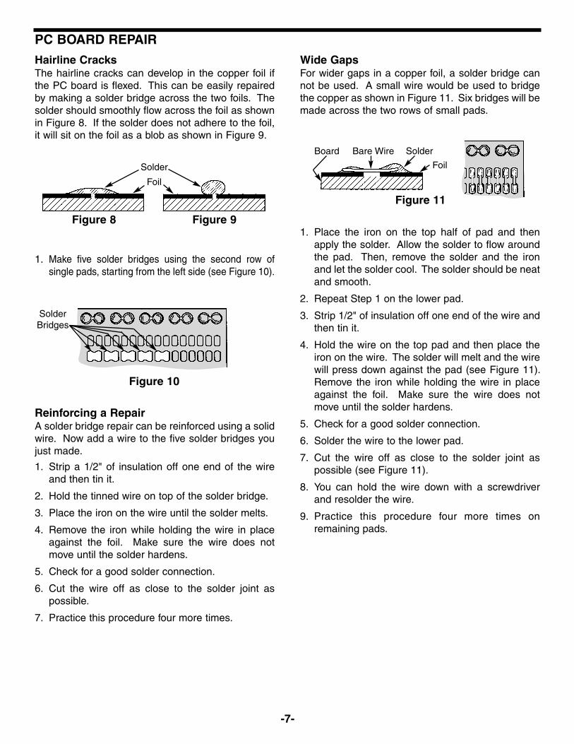
Hairline CracksThe hairline cracks can develop in the copper foil ifthe PC board is flexed. This can be easily repairedby making a solder bridge across the two foils. Thesolder should smoothly flow across the foil as shownin Figure 8. If the solder does not adhere to the foil,it will sit on the foil as a blob as shown in Figure 9.
1. Make five solder bridges using the second row ofsingle pads, starting from the left side (see Figure 10).
Reinforcing a RepairA solder bridge repair can be reinforced using a solidwire. Now add a wire to the five solder bridges youjust made.
1. Strip a 1/2" of insulation off one end of the wireand then tin it.
2. Hold the tinned wire on top of the solder bridge.
3. Place the iron on the wire until the solder melts.
4. Remove the iron while holding the wire in placeagainst the foil. Make sure the wire does notmove until the solder hardens.
5. Check for a good solder connection.
6. Cut the wire off as close to the solder joint aspossible.
7. Practice this procedure four more times.
Wide GapsFor wider gaps in a copper foil, a solder bridge cannot be used. A small wire would be used to bridgethe copper as shown in Figure 11. Six bridges will bemade across the two rows of small pads.
1. Place the iron on the top half of pad and thenapply the solder. Allow the solder to flow aroundthe pad. Then, remove the solder and the ironand let the solder cool. The solder should be neatand smooth.
2. Repeat Step 1 on the lower pad.
3. Strip 1/2" of insulation off one end of the wire andthen tin it.
4. Hold the wire on the top pad and then place theiron on the wire. The solder will melt and the wirewill press down against the pad (see Figure 11).Remove the iron while holding the wire in placeagainst the foil. Make sure the wire does notmove until the solder hardens.
5. Check for a good solder connection.
6. Solder the wire to the lower pad.
7. Cut the wire off as close to the solder joint aspossible (see Figure 11).
8. You can hold the wire down with a screwdriverand resolder the wire.
9. Practice this procedure four more times onremaining pads.
Figure 8 Figure 9
Solder
Foil
Figure 11
Solder
Foil
Bare WireBoard
Figure 10
SolderBridges
PC BOARD REPAIR

-8-
Desoldering wick is a braided wire coated with non-corrosive rosin flux. It is the simplest and safest toolfor removing solder from a solder connection. Whenthe braided wire is heated, the flux cleans andbreaks up the surface tension so the melted solder
from the connection flows into the braid by capillaryaction.
Included in this kit is a six inch length of solder wick(desoldering braid).
Place the solder wick on one of the pads and theiron on top of it (see Figure 12).
As the solder melts, it will be drawn into the wick.
When the iron and wick are removed, the soldershould be removed. You need to repeat theprocess if some solder remains.
If necessary, repeat the procedure until all of theunwanted solder is removed.
After the excess solder has been wicked away by thedesoldering braid, clip off and discard the solder-saturated portion of the braid. For best results,always use a fresh area of the braid for eachprocedure.
Figure 12
Figure 13
Using solder wick to remove excess solder.
A close-up view of the accumulation of solder ontothe solder wick (desoldering braid).
Excess Solder
Solder Wick
Soldering Iron Tip
Foil Side of PC board
CAUTION: Wick getsHOT - use long nosepliers to hold wick.
REMOVING EXCESS SOLDER USING SOLDER WICK
Using the Solder Wick
-9-
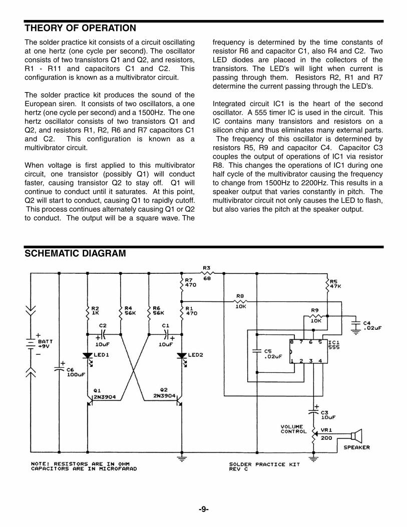
The solder practice kit consists of a circuit oscillatingat one hertz (one cycle per second). The oscillatorconsists of two transistors Q1 and Q2, and resistors,R1 - R11 and capacitors C1 and C2. Thisconfiguration is known as a multivibrator circuit.
The solder practice kit produces the sound of theEuropean siren. It consists of two oscillators, a onehertz (one cycle per second) and a 1500Hz. The onehertz oscillator consists of two transistors Q1 andQ2, and resistors R1, R2, R6 and R7 capacitors C1and C2. This configuration is known as amultivibrator circuit.
When voltage is first applied to this multivibratorcircuit, one transistor (possibly Q1) will conductfaster, causing transistor Q2 to stay off. Q1 willcontinue to conduct until it saturates. At this point,Q2 will start to conduct, causing Q1 to rapidly cutoff.This process continues alternately causing Q1 or Q2to conduct. The output will be a square wave. The
frequency is determined by the time constants ofresistor R6 and capacitor C1, also R4 and C2. TwoLED diodes are placed in the collectors of thetransistors. The LED's will light when current ispassing through them. Resistors R2, R1 and R7determine the current passing through the LED’s.
Integrated circuit IC1 is the heart of the secondoscillator. A 555 timer IC is used in the circuit. ThisIC contains many transistors and resistors on asilicon chip and thus eliminates many external parts.The frequency of this oscillator is determined by
resistors R5, R9 and capacitor C4. Capacitor C3couples the output of operations of IC1 via resistorR8. This changes the operations of IC1 during onehalf cycle of the multivibrator causing the frequencyto change from 1500Hz to 2200Hz. This results in aspeaker output that varies constantly in pitch. Themultivibrator circuit not only causes the LED to flash,but also varies the pitch at the speaker output.
THEORY OF OPERATION
SCHEMATIC DIAGRAM

What Good Soldering Looks LikeA good solder connection should be bright, shiny,smooth, and uniformly flowed over all surfaces.
Soldering a PC board1. Solder all components from the copper foil side
only. Push the soldering iron tip against both thelead and the circuit board foil.
2. Apply a small amount of solder to the iron tip.This allows the heat to leave the iron and ontothe foil. Immediately apply solder to theopposite side of the connection, away from theiron. Allow the heated component and thecircuit foil to melt the solder.
3. Allow the solder to flow around the connection.Then, remove the solder and the iron and let theconnection cool. The solder should have flowedsmoothly and not lump around the wire lead.
4. Here is what a good solder connection looks like.
Types of Poor Soldering Connections
1. Insufficient heat - the solder will not flow ontothe lead as shown.
2. Insufficient solder - let the solder flow over theconnection until it is covered. Use just enoughsolder to cover the connection.
3. Excessive solder - could make connectionsthat you did not intend to between adjacent foilareas or terminals.
Heat SinkingElectronic components such as transistors, IC’s, anddiodes can be damaged by the heat duringsoldering. Heat sinking is a way of reducing the heaton the components while soldering. Dissipating theheat can be achieved by using long nose pliers, analligator clip, or a special heat dissipating clip. Theheat sink should be held on the component leadbetween the part and the solder joint.
SOLDERINGA poorly soldered joint can greatly affect small current flow in circuits and can cause equipment failure. You candamage a PC board or a component with too much heat or cause a cold solder joint with insufficient heat.Sloppy soldering can cause bridges between two adjacent foils preventing the circuit from functioning.
Solder Soldering Iron
Foil
Solder
Soldering Iron
Foil
Component Lead
Soldering Iron
Circuit Board
Foil
Rosin
Soldering iron positionedincorrectly.
Solder
GapComponent Lead
Solder
Heat Sink(this can be ordered as part of Elenco’sSolder Ease Kit Model SE-1).
Soldering IronSolder
Heat SensitiveComponent (Diode)
PC Board
-10-
-11-
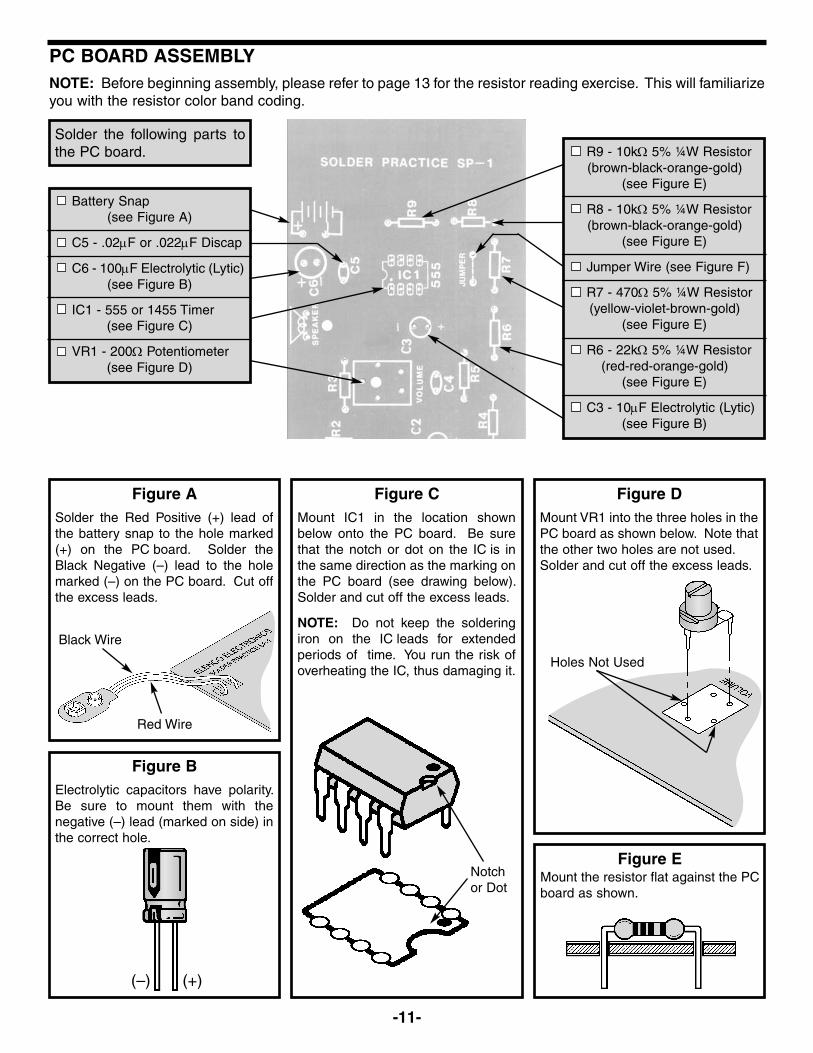
PC BOARD ASSEMBLYNOTE: Before beginning assembly, please refer to page 13 for the resistor reading exercise. This will familiarizeyou with the resistor color band coding.
Battery Snap(see Figure A)
C5 - .02μF or .022μF Discap
C6 - 100μF Electrolytic (Lytic)(see Figure B)
IC1 - 555 or 1455 Timer(see Figure C)
VR1 - 200Ω Potentiometer(see Figure D)
R9 - 10kΩ 5% ¼W Resistor(brown-black-orange-gold)
(see Figure E)
R8 - 10kΩ 5% ¼W Resistor(brown-black-orange-gold)
(see Figure E)
Jumper Wire (see Figure F)
R7 - 470Ω 5% ¼W Resistor(yellow-violet-brown-gold)
(see Figure E)
R6 - 22kΩ 5% ¼W Resistor(red-red-orange-gold)
(see Figure E)
C3 - 10μF Electrolytic (Lytic)(see Figure B)
Figure EMount the resistor flat against the PCboard as shown.
Figure BElectrolytic capacitors have polarity.Be sure to mount them with thenegative (–) lead (marked on side) inthe correct hole.
(+)(–)
Figure ASolder the Red Positive (+) lead ofthe battery snap to the hole marked(+) on the PC board. Solder theBlack Negative (–) lead to the holemarked (–) on the PC board. Cut offthe excess leads.
Figure CMount IC1 in the location shownbelow onto the PC board. Be surethat the notch or dot on the IC is inthe same direction as the marking onthe PC board (see drawing below).Solder and cut off the excess leads.
NOTE: Do not keep the solderingiron on the IC leads for extendedperiods of time. You run the risk ofoverheating the IC, thus damaging it.
Figure DMount VR1 into the three holes in thePC board as shown below. Note thatthe other two holes are not used.Solder and cut off the excess leads.
Solder the following parts tothe PC board.
Notchor Dot
Red Wire
Black Wire
Holes Not Used

-12-
Figure HMount the LED onto the PC boardwith the flat side of the LED in thesame direction as marked on the PCboard. Be sure to mount the LEDflush with the PC board as shownbelow.Solder and cut off the excess leads.
Figure G Mount the IC with the flat side in thesame direction as marked on the PCboard. Leave about 1/8” of spacebetween the transistor and the PCboard as shown below. Solder andcut off the excess leads.
PC BOARD ASSEMBLY (continued)
Figure FCut a 1” wire and strip 1/8” ofinsulation off of both ends.
R3 - 68Ω 5% ¼W Resistor(blue-gray-black-gold)
(see Figure E)
R2 - 1kΩ 5% ½W Resistor(brown-black-red-gold)
(see Figure E)
C2 - 10μF Electrolytic (Lytic)(see Figure B)
Q1 - 2N3904 TransistorQ2 - 2N3904 Transistor
(see Figure G)
LED1 - Light Emitting Diode(see Figure H)
R5 - 47kΩ 5% ¼W Resistor(yellow-violet-orange-gold)
(see Figure E)
R4 - 22kΩ 5% ¼W Resistor(red-red-orange-gold)
(see Figure E)
C4 - .02μF or .022μF Discap
C1 - 10μF Electrolytic (Lytic)(see Figure B)
R1 - 470Ω 5% ¼W Resistor(yellow-violet-brown-gold)
(see Figure E)
Jumper Wire (see Figure F)
LED2 - Light Emitting Diode(see Figure H)
Flat
1/8”
OPERATIONAfter completing the assembly of the kit, double back to see that the soldering looks good and all of thecomponents are in their proper place. If everything is all right, attach the 9V battery to the battery snap. TheLED’s should alternately light and the speaker should sound a wobbling siren.Continue to the Desoldering Practice/Component Replacement Secton.
Note: Refer to the Troubleshooting Section if your circuit does not work.
Flat
Mount Flushto PC Board
Cut the 12” wire in half and the strip1/8” of insulation off of both ends.Insert the speaker wire through thePC board as shown. Then, insertthe wires into the speaker holesand solder. Solder the other end ofthe wires to the speaker.
Solder the following parts tothe PC board.

-13-
If any parts are missing or damaged, see instructoror bookstore. DO NOT contact your place ofpurchase as they will not be able to help you.Contact Elenco® Electronics (address/phone/e-mailis at the back of this manual).
If you are experiencing a problem, first read thetheory of operation to familiarize yourself with theoperation.
Component Check
1. Be sure that all components have been mountedin their correct places.
2. Make sure that C1 and C2, the electrolyticcapacitor is mounted correctly. The negative leadshould be in the hole as shown on the top legend.
3. Have LED’s LED1 and LED2 been installedcorrectly? The flat side of their bodies should bein the same direction as marked on the toplegend. If the LED’s are in backwards, they willnot light.
4. Pay close attention to the red and black wires ofthe battery snap. The red wire should be installedin the positive (+) hole and the black wire in thenegative (–) hole. Snap in a fresh 9-volt battery.
Problems
1. No LED’s Light
• Check the solder connections for the batterywires and switch.
• Check that all parts are in the correct way.
2. LED1 Does Not Light
• Check C1, LED1 and Q1.
3. LED2 Does Not Light
• Check C2, LED2 and Q2.
4. LED1 or LED2 is Always On
• Check C1 and C2 for opens.
• Check Q1 and Q2 for shorts.
Remember that there are two oscillators. If no soundcomes out of the speaker, but the LED flashesalternately, then the 555 timer is not working. Besure that the volume control is at maximum. Checkthe components IC1, R5, R8, R9, C3, C4 and C5. Besure that the IC is in properly.
If a steady sound (not wobbling) comes out of thespeaker, then the multivibrator is not working. Checkthe components associated with transistor Q1 andQ2. Check the LED by shorting the transistorcollector to the emitter. The LED should light. If not,then the LED is either open or backward.
TROUBLESHOOTING
In this exercise you will replace the 22kΩ resistorsR4 and R6 with two 56kΩ resistors. You unsolder theresistors using the solder wick and then install newresistors.
1. Remove the battery from the battery snap.
2. Locate the pads that resistor R4 is soldered to.
3. Place the solder wick on one of the pads and theiron on top of it (refer to page 8).
4. As the solder melts, it will be drawn into the wick.
5. When the iron and wick are removed, the soldershould be removed. You need to repeat theprocess if some solder remains.
6. Unsolder the other lead and remove then removethe resistor.
7. Follow the same procedure and remove resistor R6.
Now use the resistors R4A and R6A mounted on thecomponent card, and install them on the PC board.Reconnect the battery and the kit should oscillate atthe correct frequency.
DESOLDERING PRACTICE/COMPONENT REPLACEMENT

-14-
WORD GLOSSARY
Capacitor An electrical component that canstore electrical pressure (voltage)for periods of time.
Cold Solder Joint Occurs because insufficient heatwas applied or the connectionwas moved before the solder hadset. Connection looks crystalline,crumbly, or dull.
Flux A substance that is used tocleanse the surface of oxidebefore it is soldered. Alwaysused in electronics work. Most ofthe solder used in electronics hasflux built right into it.
Heat Sinking A process of keeping thecomponent from becomingoverheated during soldering. Anymetal object that can be clampedto the component lead will workas an effective heat sink. Analligator clip or pliers work well.
Integrated Circuit (IC) A type of circuit in whichtransistors, diodes, resistors, andcapacitors are all constructed ona semiconductor base.
Jumper Wire A wire that is connected from oneplace to another on a PC board,thereby making a connectionbetween two pads.
LED Common abbreviation for lightemitting diode.
Light Emitting Diode A diode made from galliumarsenide that has a turn-onenergy so high that light isgenerated when current flowsthrough it.
Oxidation Most metals, when exposed toair, form an oxide on their surfacewhich prevents solder fromadhering to the metal.
Polarity The division of two opposingforces or properties.
Printed Circuit Board A board used for mountingelectrical components. Components are connectedusing metal traces “printed” onthe board instead of wires.
Resistor Component used to control theflow of electricity in a circuit. It ismade of carbon.
Rosin Core Solder The most common type of solderused in electronics generallyreferred to as 63/37 rosin coresolder.
Solder A tin/lead alloy that melts at avery low temperature, used tojoin other metals together. Itproduces excellent electricalconnections.
Solder Bridge An unwanted solder connectionbetween two points that are closetogether.
Solder Melting Point The temperature at which atin/lead alloy (solder) melts. Thecommon solder used inelectronics (63% tin / 37% lead)has a melting point of 370OF.
Solder Wick Braided wire coated with flux toeffectively remove solder from aconnection.
Soldering The process of joining two ormore metals by applying solder tothem.
Tack Soldering A connection where the lead orwire does not have anymechanical support.
Tinning the Tip A process of coating thesoldering iron tip with solder tominimize the formation of oxideon the tip, which would reducethe amount of heat transfer.
Transistor An electronic device that uses asmall amount of current to controla large amount of current.
Wire Gauge Refers to the size of the wire. Thebigger the number, the smallerthe diameter of the wire.18 gauge to 24 gauge isgenerally used for hook-up inelectronics.

Elenco® Electronics, Inc.150 Carpenter Avenue • Wheeling, IL 60090
Phone: (847) 541-3800 • Fax: (847) 520-0085Web site: www.elenco.com • e-mail: [email protected]
1. Solder is comprised of what two materials?A. Gold and copperB. Tin and leadC. Zinc and copperD. Lead and aluminum
2. What type of flux should be used in electronics?A. ChlorideB. OrganicC. RosinD. Corrosive
3. When working on PC boards, what wattage rangeof iron is ideal?A. 15-40 wattsB. 50-100 wattsC. 1-10 wattsD. 100-200 watts
4. Tinning the soldering tip will prevent it from . . .A. heating.B. melting.C. soldering.D. oxidizing.
5. Proper solder adhesion requires that the metalsurface to be . . .A. solder free.B. clean.C. greasy.D. cold.
6. Solder wick is used to . . .A. remove solder.B. solder in small parts.C. cleaning the soldering iron tip.D. removing flux.
7. A cold solder joint is caused by . . .A. a solder bridge.B. using 60/40 solder.C. insufficient heat.D. acid core solder.
8. When two adjacent foils accidentally touch, it iscalled . . .A. a jumper.B. a blob.C. a solder hole.D. a solder bridge.
9. What ratio has the greatest amount of tin?A. 20/60B. 40/60C. 50/50D. 60/40
10. A good solder connection should be . . .A. dull and rough.B. shiny, bright and smooth.C. lumped around the connection.D. soldered on one side of the connection.
QUIZ
Answers:1. B, 2. C, 3. A, 4. D, 5. B, 6. A, 7. C, 8. D, 9. D, 10. B