mocvd routes to 2d crystals - homepage - cmu ... research institute 2d at penn state mauricio...
TRANSCRIPT
MATERIALS RESEARCH INSTITUTE
MOCVD Routes to 2D Crystals
Joan M. Redwing
Department of Materials Science & Engineering
Materials Research Institute Center for Two-Dimensional and Layered Materials (2DLM)
The Pennsylvania State University University Park, PA 16802 USA

MATERIALS RESEARCH INSTITUTE 2D at Penn State
Mauricio Terrones Joshua Robinson
Dire
cto
r
Asso
c.D
ire
cto
r
Est. 2013
2
20+ Faculty and 45
+ Students/Post-docs
Michael Abraham
Amin Azizi
Zakaria Al Balushi
Ganesh Bhimanapati
Donna D. Deng
Anna Domask
Haila Al Dosari
Dr. Sarah Eichfeld
Dr. Ana Laura Elias
Simin Feng
Robert Fraleigh
Jarod Gagnon
Yiyang Gong
Corey T. Janisch
Ethan Kahn
Nina Kovtyukhova
Chia-Hui (Candace) Lee
Yu-Chuan Lin
Minh An Nguyen
Lavish Pabbi
Nestor Perea
Lakshmy Rajukumar
Chris Rotella
Dr Eduardo Cruz Silva
Ivan Skachko
Yifan Sun
Youjian Tang
Timothy Walter
Junjie Wang
Yuanxi Wang
Zefang Wang
Xiaoxiang Xi
Kehao Zhang
Xiaotian Zhang
Liang Zhao
Rui Zhao
Chanjing Zhou
Zhong Lin
Debangshu Mukherjee
Roger Walker
Shruti Subramanian
Nasim Alem
Vincent Crespi
Ismaila Dabo
Suman Datta
Aman Haque
Eric Hudson
Tom Jackson
Ying Liu
Zhiwen Liu
Kin Fai Mak
Tom Mallouk
Theresa Mayer
Suzanne Mohney
Joan Redwing
Joshua Robinson
Nitin Samarth
Jie Shan
Jorge Sofo
Mauricio Terrones
Sulin Zhang
Jun Zhu
Faculty Students/Post-docs

MATERIALS RESEARCH INSTITUTE Layered Materials
Q.H. Huang, et al. Nature Nanotech. 7 (2012) p. 699
• Graphene-like layered materials
• Exhibit wide variety of electronic properties –
insulators, semiconductors, semi-metals,
superconductors

MATERIALS RESEARCH INSTITUTE
S. Das, J.A. Robinson, M. Terrones, et al.
Annual Review of Materials Research, 45 , 1-27 (2015)
4
The TMD Synthesis “Atlas”

MATERIALS RESEARCH INSTITUTE
• Highly scalable process
• Excellent control over
W:Se ratio
850 oC 900 oC
600 Torr 500 Torr 700 Torr
INCREASING DOMAIN SIZE 800 oC
T =
75
0oC
P
= 7
00
To
rr
500 nm 500 nm
500 nm 500 nm 500 nm
0 nm
10 nm
50 nm
WSe2 SiO2
SiC
W-rich WSe2
Tungsten Diselenide (WSe2)
S.M. Eichfeld, J.M. Redwing, J.A. Robinson, et al., ACS Nano, 2015, 9 (2), pp 2080–2087
Metalorganic Chemical Vapor Deposition

MATERIALS RESEARCH INSTITUTE
• Defects serve as nucleation
sites in 2D materials.
• Typical defects are
chalcogen (S,Se,Te)
vacancies. Wallace Group (UT Dallas)
WSe2
Se:W Ratio: 400 Se:W Ratio: 800 Se:W Ratio: 170 Se:W Ratio: 14000
Temp (°C) Time (min) Pre- Anneal Pressure (Torr)
800 30 500C, 15min 700
Se:W ratio has
significant impact on
domain size, shape,
and “defect” formation
0.0 2.0x10⁴
1.0x1051.5x10
50
1
2
3
4 WSe
2/Sapphire
WSe2/EG
Dom
ain
siz
e (
m)
Se to W ratio
Tungsten Diselenide (WSe2)

MATERIALS RESEARCH INSTITUTE
7
WSe2 on Free Standing Graphene Templates
After MOCVD Growth As Prepared
A. Azizi, N. Alem, et al. ACS Nano 9 (2015) 4882.
• Developed process to produce freestanding
van der Waals heterostructures
• Ideal for investigating layer-layer interaction
with graphene

MATERIALS RESEARCH INSTITUTE
8
WSe2 – Epitaxy and Defects
(a) HAADF-STEM image of monolayer and multilayer WSe2
HAADF-STEM images of (b) monolayer WSe2 and (c) edge
region showing W-termination
d) TEM image showing nucleation near grain boundary in
graphene
(a) TEM image and (b) SAD pattern showing
epitaxial relationship between WSe2 and graphene
(c) Structural model showing alignment of W atoms
in WSe2 and C atoms in graphene (circled in red)

MATERIALS RESEARCH INSTITUTE Pulsed MOCVD growth of GaN
9
SiC Substrate Epitaxial Graphene
Cross-section TEM of GaN growing between
graphene and SiC substrate
Ke Wang, PSU MCL
2 nm
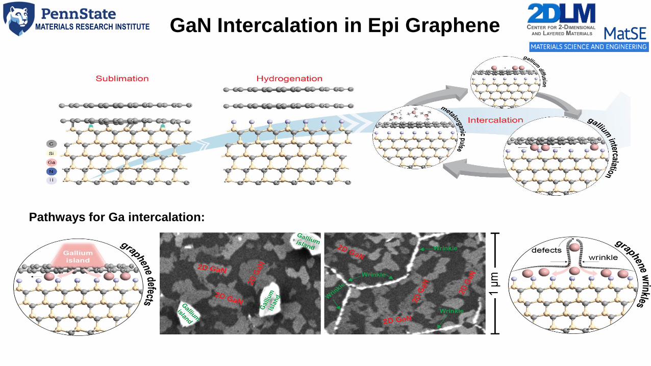
MATERIALS RESEARCH INSTITUTE GaN Intercalation in Epi Graphene
Pathways for Ga intercalation:
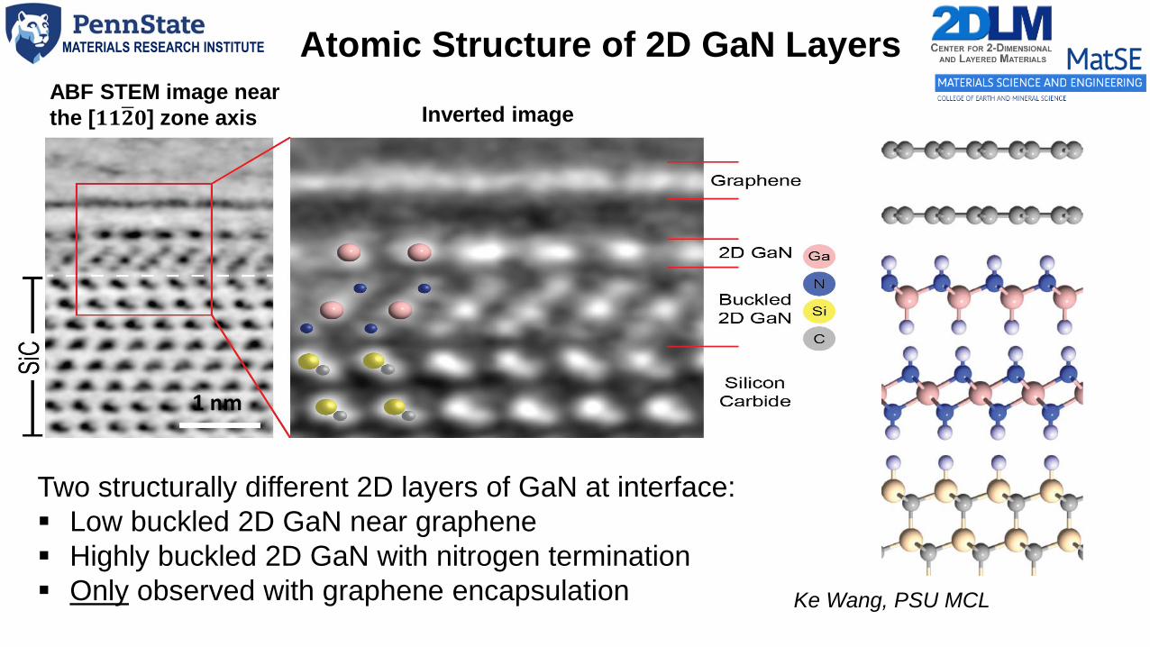
MATERIALS RESEARCH INSTITUTE Atomic Structure of 2D GaN Layers
Two structurally different 2D layers of GaN at interface:
Low buckled 2D GaN near graphene
Highly buckled 2D GaN with nitrogen termination
Only observed with graphene encapsulation
ABF STEM image near
the [𝟏𝟏𝟐 𝟎] zone axis Inverted image
Ke Wang, PSU MCL
1 nm

MATERIALS RESEARCH INSTITUTE
Electronic Structure of 2D GaN Layers
12
Predicted bandgap energies:
Low buckled GaN Eg=4.96 eV
High buckled GaN Eg=4.24 eV
Composite structure Eg=2.02 eV
Ram Krishna Ghosh and Suman Datta

MATERIALS RESEARCH INSTITUTE

MATERIALS RESEARCH INSTITUTE
14
Summary
Graduate Students
Xiaotian Zhang
Zakaria Al Balushi
Nathan Martin
Mel Hainey Jr.
Postdoctoral Scholars
Chen Chen
Jarod Gagnon
Tanushree Choudhury
PSU Collaborators
Dr. Sarah Eichfeld (MRI)
Dr. Josh Robinson (MatSE)
Dr. Nasim Alem (MatSE)
Dr. Suman Datta (EE)
Dr. Ke Wang (MRI)
Dr. Tom Jackson (EE)
Financial support provided by:
Acknowledgements
• MOCVD is a promising technique for TMDs and layered materials
• Graphene encapsulated MOCVD growth viable method to stabilize 2D GaN
• Future work directed at heterostructure growth, alloys & doping

MATERIALS RESEARCH INSTITUTE
15

MATERIALS RESEARCH INSTITUTE

MATERIALS RESEARCH INSTITUTE
Materials discovery with computation
Wurtzite Bulk Structure of GaN

MATERIALS RESEARCH INSTITUTE
Stabilized Structure
Indirect bandgap 4.12 eV
direct bandgap 5.28 eV
MATERIALS RESEARCH INSTITUTE
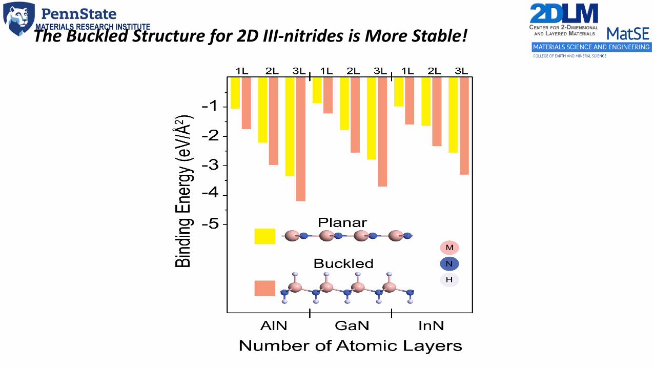
The Buckled Structure for 2D III-nitrides is More Stable!

MATERIALS RESEARCH INSTITUTE
Polarization-induced Topological insulators for memory
and quantum computing
Single-photon emitters for quantum optics and
communication
Nano Lett. 14, 982–986 (2014)
Nat. Mater. 5, 887–892 (2006)
Phys. Rev. Lett. 109, 186803 (2012)
Exotic physics