moby interface module asm 472 - siemens · 1–1 asm 472 (4) j31069-d0140-u001-a2-7618 short...
TRANSCRIPT

Table of Contents
Short Description of ASM 472 1
Configuration, Mounting andCommissioning 2
Programming the ASM 472 3
Sample Applications 4
Presence Check 5
Trouble-Shooting and Error Messages 6
Technical Data of ASM 472 7
Firmware Update A
Warnings B
Published in May 2008
Interface Module ASM 472
Technical Description and Programmer’s Guide
MOBY�
Notes on safety
This manual contains notes which must be adhered to for your own personal safety and to prevent property da-mage. The notes are highlighted with a warning triangle and graduated by amount of danger.
!Danger
Means that death, severe injury or substantial property damage will occur if these precautions arenot taken.
!Warning
Means that death, severe injury or substantial property damage may occur if these precautions arenot taken.
!Caution
Means that injury or property damage may occur if these precautions are not taken.
Note
Is an important piece of information on the product, its handling or a particular part of the documen-tation which requires special attention.
Qualified personnel
A device may only be commissioned and operated by qualified personnel. For the purpose of the safety notes inthis manual, qualified personnel are those persons who are authorized to commission, ground and tag devices,systems and current circuits in accordance with applicable safety standards.
Intended use
Comply with the following.
!Warning
The product may only be used for the applications described in the catalog and the technical des-cription and only in connection with Siemens equipment or devices and components of other manu-facturers recommended by Siemens.
Correct and safe operation of the product is based on correct transportation, correct storage, setupand installation as well as careful operator control and maintenance.
Brand names
SIMATIC� and MOBY� are registered brand names of SIEMENS AG.
The other designations in this publication may be brand names whose use by third parties for their own purposesmay violate the rights of the owner.
Although we have checked this publication for agreement with the actualhardware and software, we cannot fully exclude differences and do not ac-cept liability for full agreement. The information in this publication is checkedat regular intervals and necessary changes included in the next release. Yoursuggestions and ideas are welcome (use the form at the end of this manual).
Disclaimer of liabilityCopyright Siemens AG 2001, 2002, 2008 All rights reserved
Reproduction, utilization and revelation of the contents of this manual isprohibited unless express permission is obtained. Violations will beprosecuted. All rights reserved particularly when a patent is granted or a utilitymodel is registered.
Siemens AGIndustry SectorPostfach 4848, D-90327 Nuremberg
� Siemens AG 2002Subject to technical change without prior notice
Siemens Aktiengesellschaft

IASM 472 (4) J31069-D0140-U001-A2-7618
Table of Contents
1 Short Description of the ASM 472 1–1. . . . . . . . . . . . . . . . . . . . . . . . . . . . . . . . . . . . . . . .
2 Configuration, Mounting and Commissioning 2–1. . . . . . . . . . . . . . . . . . . . . . . . . . . .
2.1 Configuration 2–1. . . . . . . . . . . . . . . . . . . . . . . . . . . . . . . . . . . . . . . . . . . . . . . . . . .
2.2 Commissioning 2–6. . . . . . . . . . . . . . . . . . . . . . . . . . . . . . . . . . . . . . . . . . . . . . . . .
3 Programming the ASM 472 3–1. . . . . . . . . . . . . . . . . . . . . . . . . . . . . . . . . . . . . . . . . . . . . .
3.1 The Process Image 3–2. . . . . . . . . . . . . . . . . . . . . . . . . . . . . . . . . . . . . . . . . . . . . .
3.2 The Command Set 3–4. . . . . . . . . . . . . . . . . . . . . . . . . . . . . . . . . . . . . . . . . . . . . .
3.3 The Status bytes 3–9. . . . . . . . . . . . . . . . . . . . . . . . . . . . . . . . . . . . . . . . . . . . . . . .
3.4 Handshake Procedure 3–10. . . . . . . . . . . . . . . . . . . . . . . . . . . . . . . . . . . . . . . . . . .
3.5 Processing Data Memories 3–13. . . . . . . . . . . . . . . . . . . . . . . . . . . . . . . . . . . . . . .
3.6 Programming New Start and Restart 3–20. . . . . . . . . . . . . . . . . . . . . . . . . . . . . . .
4 Sample Applications 4–1. . . . . . . . . . . . . . . . . . . . . . . . . . . . . . . . . . . . . . . . . . . . . . . . . . . .
4.1 Programming Example for Allen Bradley 4–2. . . . . . . . . . . . . . . . . . . . . . . . . . . .
4.2 The ECC Driver 4–7. . . . . . . . . . . . . . . . . . . . . . . . . . . . . . . . . . . . . . . . . . . . . . . . .
5 Presence Check 5–1. . . . . . . . . . . . . . . . . . . . . . . . . . . . . . . . . . . . . . . . . . . . . . . . . . . . . . . .
5.1 Definition of Terms 5–2. . . . . . . . . . . . . . . . . . . . . . . . . . . . . . . . . . . . . . . . . . . . . .
5.2 Presence Check Switched Off 5–3. . . . . . . . . . . . . . . . . . . . . . . . . . . . . . . . . . . . .
5.3 Presence Check Switched On 5–4. . . . . . . . . . . . . . . . . . . . . . . . . . . . . . . . . . . . .
5.4 Startup of the ASM 472 5–5. . . . . . . . . . . . . . . . . . . . . . . . . . . . . . . . . . . . . . . . . .
6 Trouble-Shooting and Error Messages 6–1. . . . . . . . . . . . . . . . . . . . . . . . . . . . . . . . . . .
6.1 Indicator Elements on the ASM 472 6–2. . . . . . . . . . . . . . . . . . . . . . . . . . . . . . . .
6.2 General Errors 6–3. . . . . . . . . . . . . . . . . . . . . . . . . . . . . . . . . . . . . . . . . . . . . . . . . .
6.3 Evaluating Errors in the Status Byte 6–4. . . . . . . . . . . . . . . . . . . . . . . . . . . . . . .
6.4 Pure Hardware Errors 6–10. . . . . . . . . . . . . . . . . . . . . . . . . . . . . . . . . . . . . . . . . . . .
7 Technical Data of the ASM 472 7–1. . . . . . . . . . . . . . . . . . . . . . . . . . . . . . . . . . . . . . . . . . .
A Firmware Update A–1. . . . . . . . . . . . . . . . . . . . . . . . . . . . . . . . . . . . . . . . . . . . . . . . . . . . . . .
B Warnings B–1. . . . . . . . . . . . . . . . . . . . . . . . . . . . . . . . . . . . . . . . . . . . . . . . . . . . . . . . . . . . . .

Komponenten Helvetica 10pt
IIASM 472
(4) J31069-D0140-U001-A2-7618
Figures
1-1 ASM 472 1–1. . . . . . . . . . . . . . . . . . . . . . . . . . . . . . . . . . . . . . . . . . . . . . . . . . . . . . . 2-1 Configurator for ASM 472 2–2. . . . . . . . . . . . . . . . . . . . . . . . . . . . . . . . . . . . . . . . 2-2 Maximum configuration of ASM 472 in one ET 200X 2–3. . . . . . . . . . . . . . . . . 2-3 Connection plug for ASM 472 ↔ SLG (6GT2 090-0BC00) 2–4. . . . . . . . . . . . 2-4 Connection cable for ASM 472 ↔ SLG (6GT2 091-1CH20) 2–4. . . . . . . . . . . 2-5 Pin allocation of the ASM 472 2–5. . . . . . . . . . . . . . . . . . . . . . . . . . . . . . . . . . . . . 2-6 Dimensions for mounting holes for basic and expansion module 2–5. . . . . . . 3-1 Placing the ASM 472 in a system 3–1. . . . . . . . . . . . . . . . . . . . . . . . . . . . . . . . . . 4-1 Program structure 4–2. . . . . . . . . . . . . . . . . . . . . . . . . . . . . . . . . . . . . . . . . . . . . . . 4-2 M-INIT 4–3. . . . . . . . . . . . . . . . . . . . . . . . . . . . . . . . . . . . . . . . . . . . . . . . . . . . . . . . . 4-3 M-MAIN 4–4. . . . . . . . . . . . . . . . . . . . . . . . . . . . . . . . . . . . . . . . . . . . . . . . . . . . . . . . 4-4 M-RESET 4–5. . . . . . . . . . . . . . . . . . . . . . . . . . . . . . . . . . . . . . . . . . . . . . . . . . . . . . 4-5 M-READ 4–6. . . . . . . . . . . . . . . . . . . . . . . . . . . . . . . . . . . . . . . . . . . . . . . . . . . . . . . 5-1 Scanning the field 5–4. . . . . . . . . . . . . . . . . . . . . . . . . . . . . . . . . . . . . . . . . . . . . . . 6-1 Pin allocation and LEDs of the ASM 472 6–2. . . . . . . . . . . . . . . . . . . . . . . . . . . . A-1 Placing an ASM 473 A–2. . . . . . . . . . . . . . . . . . . . . . . . . . . . . . . . . . . . . . . . . . . . . A-2 Calling the firmware update A–3. . . . . . . . . . . . . . . . . . . . . . . . . . . . . . . . . . . . . . .
Tables
1-1 Ordering data 1–2. . . . . . . . . . . . . . . . . . . . . . . . . . . . . . . . . . . . . . . . . . . . . . . . . . . 2-1 Example of a RESET command 2–7. . . . . . . . . . . . . . . . . . . . . . . . . . . . . . . . . . . 3-1 Available memory capacities 3–13. . . . . . . . . . . . . . . . . . . . . . . . . . . . . . . . . . . . . . 3-2 Address space of MDS versions for MOBY I, E, F, U and D 3–14. . . . . . . . . . . 3-3 Address space of the transponder versions for RF300 3–16. . . . . . . . . . . . . . . . 3-4 Initialization duration 3–19. . . . . . . . . . . . . . . . . . . . . . . . . . . . . . . . . . . . . . . . . . . . . 4-1 Data structure of a 62-byte MDS 4–8. . . . . . . . . . . . . . . . . . . . . . . . . . . . . . . . . . 6-1 Error messages of the ASM 472 6–4. . . . . . . . . . . . . . . . . . . . . . . . . . . . . . . . . . . 6-2 Pure hardware errors 6–10. . . . . . . . . . . . . . . . . . . . . . . . . . . . . . . . . . . . . . . . . . . . 7-1 Technical data 7–1. . . . . . . . . . . . . . . . . . . . . . . . . . . . . . . . . . . . . . . . . . . . . . . . . . 7-2 MOBY times with presence check 7–2. . . . . . . . . . . . . . . . . . . . . . . . . . . . . . . . . 7-3 Transmission times to the MDS (MOBY I) 7–3. . . . . . . . . . . . . . . . . . . . . . . . . .

1–1ASM 472 (4) J31069-D0140-U001-A2-7618
Short Description of the ASM 472
Description
The ASM 472 interface module is a MOBY module for connection to DeviceNet. Itcan be installed on the basic module (5136-DNS-200X). The DeviceNet bus han-dles communication of the basic module with the user. Any number of DeviceNetscanners can be used.
The MDS data are accessed by physically addressing the MDS.
The master controller requires a function block if the ASM 472 is run in a Device-Net environment. This function block can be programmed by the user with just afew commands. For details on programming, see chapter 3 which offers a detailedinterface description.
Other features:
� Up to 7 ASM 472s can be run at the same time in one DeviceNet station.
� All I/O modules from the ET 200X family can be run parallel to the ASM 472.
� The interface description of the ASM 472 is available for any DeviceNet scan-ners.
� Compatibility: The ASM 472 is compatible with all SLGs and MDSs of theMOBY I/E/F/U/D and RF300 family.
� Errors of the ASM 472 are indicated by its LEDs and also on the programmerinterface for the user.
Figure 1-1 ASM 472
1

Komponenten Helvetica 10pt
1–2ASM 472
(4) J31069-D0140-U001-A2-7618
Ordering data
Table 1-1 Ordering data
Product Description Order No.
ASM 472 interface module 6GT2 002-0FB00
Accessories MOBY E, I, U:SLG cable (2 m = standard cable)SLG cable (5 m)SLG cable (10 m)SLG cable (20 m)SLG cable (50 m)SLG cable (2 m) with straight SLG plug
6GT2 091-1CH206GT2 091-1CH506GT2 091-1CN106GT2 091-1CN206GT2 091-1CN506GT2 091-2CH20
Accessories MOBY D, F:SLG cable (2 m = standard cable)SLG cable (5 m)SLG cable (20 m)
6GT2 491-1CH206GT2 491-1CH506GT2 491-1CN20
Accessories RF300:Connection cable ASM 472 ↔ Reader RF3xxRStub line, fabricated Length 2 m (standard length)Length 5 m
6GT2 891-1CH206GT2 891-1CH50
for cable fabrication by the customer for lengths� 50 m:ASM connection plug without cableSLG connection plug (1 each)Cable without plug, 6 x 0.25 mm2, 50 mCable without plug, 6 x 0.25 mm2, 120 mCable without plug, 6 x 0.25 mm2, 500 m
6GT2 090-0BC006GT2 090-0BA006GT2 090-0AN506GT2 090-0AT126GT2 090-0AT50
Software Customer-specific
“RFID systems software & documentation” CDwith all RFID documentations 6GT2 080-2AA10

2–1ASM 472 (4) J31069-D0140-U001-A2-7618
Configuration, Mounting and Commissioning
2.1 Configuration
!Caution
Always adhere to the User’s Guide “5136-DNS-200X DeviceNet Slave Adapter”when configuring, mounting and commissioning the ASM 472.
You will find special information here on mounting, power supplies and wiringground.
2

Configuration, Mounting and Commissioning
2–2ASM 472
(4) J31069-D0140-U001-A2-7618
Configurator – ASM 472
DeviceNet scanner
SLG
MDS
2 m(standard cablelength)
CAN line to all DeviceNet slaves
24 V for ET 200Xelectronics, Device-Net bus and MOBYSLG
Up to 126 DeviceNetmodules can be run onone scanner.
Figure 2-1 Configurator for ASM 472
Configuration, Mounting and Commissioning
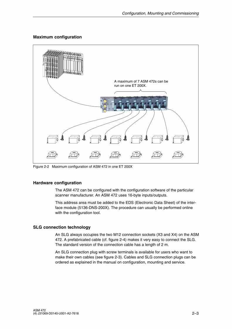
2–3ASM 472 (4) J31069-D0140-U001-A2-7618
Maximum configuration
A maximum of 7 ASM 472s can berun on one ET 200X.
Figure 2-2 Maximum configuration of ASM 472 in one ET 200X
Hardware configuration
The ASM 472 can be configured with the configuration software of the particularscanner manufacturer. An ASM 472 uses 16-byte inputs/outputs.
This address area must be added to the EDS (Electronic Data Sheet) of the inter-face module (5136-DNS-200X). The procedure can usually be performed onlinewith the configuration tool.
SLG connection technology
An SLG always occupies the two M12 connection sockets (X3 and X4) on the ASM472. A prefabricated cable (cf. figure 2-4) makes it very easy to connect the SLG.The standard version of the connection cable has a length of 2 m.
An SLG connection plug with screw terminals is available for users who want tomake their own cables (see figure 2-3). Cables and SLG connection plugs can beordered as explained in the manual on configuration, mounting and service.

Configuration, Mounting and Commissioning
2–4ASM 472
(4) J31069-D0140-U001-A2-7618
SLG cable: 6GT2 090-0A���
PG 11 screw; Max. cable diameter = 6.5 mm(Don’t tighten screw until plug is assem-bled.)
2 screws to openthe plug
Coupling plug M12 onASM 472
1234
56SS
Plug Pin
1
2
3
4
5
6
S
S
Core Color
Green
White
Brown
Yellow
Gray
Pink
- (nc)
Shield
Connection toPin of SLGPlug
4
6
1
5
3
2
-
Plug covering hood removed
Protection rating IP 67
48
18.5
Figure 2-3 Connection plug for ASM 472 ↔ SLG (6GT2 090-0BC00)
6
1
4
5
3
2
Two 5-pin round M12plugs
X1/2
X1/3
X1/1
X1/4
X2/3
X2/1
X1/5
X2/5
X1 X2
White
Brown
Green
Yellow
Gray
Pink
SLG plug (socket)
2 m *22.5
18.5
* Standard length
Figure 2-4 Connection cable for ASM 472 ↔ SLG (6GT2 091-1CH20)

Configuration, Mounting and Commissioning
2–5ASM 472 (4) J31069-D0140-U001-A2-7618
Pin allocations
The following figure describes the pin allocation to the SLG. The pin allocation isonly important when you are making your own SLG cable.
Socket Pin Allocation (SLG)
12345
+RxD+TxD–TxD–RxDPE
X3
12345
+24 Vn. c.0 Vn. c.PE
X4
Figure 2-5 Pin allocation of the ASM 472
Dimensional drawing for mounting holes
The figure below contains the dimensions for the positions of the holes for themounting screws for a basic module (5136-DNS-200X) and an expansion module(ASM 472).
n � 60120
53.5
n = number of expansion modules
28.2
5
126.8
5136-DNS-200X ASM 472
87
110
Figure 2-6 Dimensions for mounting holes for basic and expansion module

Configuration, Mounting and Commissioning
2–6ASM 472
(4) J31069-D0140-U001-A2-7618
2.2 Commissioning
Commissioning the module
After the module is connected to the interface station (5136-DNS-200X) and con-nection to the SLG is established, commissioning can begin. The interface stationmust be connected with a DeviceNet scanner and powered (see figure 2-1). Makesure that a free DeviceNet address is set for the interface station (see commission-ing of the interface station).
When the ASM module is turned on, the red ERR-LED flashes until a correct RESET command is executed (cf. figure 6-1).
Configuring the station
You cannot address the station until you configure it with the configuration tool ofyour DeviceNet scanner. The input and output areas of the interface station mustbe expanded by 16 bytes each for an ASM 472 and entered in the memory area ofthe PLC being used. The memory areas of the interface station appear first, fol-lowed by the memory areas of the expansion modules in the sequence in whichthey were connected to the interface module.
Loading the configuration
When the correct configuration is loaded in the DeviceNet scanner (i.e., the com-plete address area of the interface station with all expansion modules is ”known” tothe scanner), the green ”I/O status” LED of the interface station lights up continu-ously if the scanner is on. Flashing indicates an error in the configuration. If thishappens, check the configuration of the input and output areas of the station.
Sending commands
Commands can now be sent to the ASM 472 (see chapter 3.2) by writing the 16bytes of the output area. The responses can then be read in the input area afterconclusion of the commands. For testing purposes, you can do this by hand. Setand reset the appropriate handshake bits (S0/Q0 or S1/Q1. See chapter 3.4).

Configuration, Mounting and Commissioning
2–7ASM 472 (4) J31069-D0140-U001-A2-7618
Table 2-1 Example of a RESET command
Output Area(HEX)
Action Input Area(HEX)
Result
B0,... Startup message = 1Q0 = 1, Q1 = 1
00,21,00,00,00,… RESET command: MOBY I, ECC = 0TABTA= 0, ANW = 1
20,21,00,00,00,… S1 = 1
90,... Q1 = 0
00,21,00,00,00,… S1 = 0
30,00,1F,… Q1 = 1, RESET status
The first command to be executed is always a RESET command (see chapter3.2). After successful execution, the ERR-LED stops flashing. This concludes com-missioning.
Commands can now be executed in any sequence.

Configuration, Mounting and Commissioning
2–8ASM 472
(4) J31069-D0140-U001-A2-7618

3–1ASM 472 (4) J31069-D0140-U001-A2-7618
Programming the ASM 472
This chapter discusses how to program the ASM 472.
The following figure shows a typical setup of ASM 472 modules in a general Devi-ceNet environment. A read/write device can be connected to an ASM 472. Pro-gramming the read/write device on an ASM 472 is very easy and requires no spe-cial knowledge of the programmer. Up to seven ASM 472s can be connected toone ET 200X.
Serial
PC Controller
ET 200X
SLG SLG
ASM472
ASM472
DeviceNet
DN
5136-DNS-200X
Figure 3-1 Placing the ASM 472 in a system
3

Programming the ASM 472
3–2ASM 472
(4) J31069-D0140-U001-A2-7618
3.1 The Process Image
The commands and the handshake are coded in bytes 0 of the command and ac-knowledgment telegram.
Command telegram to ASM (PIO)
Byte 0 Command byte
Byte 1 Parameter 1 (ADR high)
2 Parameter 2 (ADR low)
3 Parameter 3 (data length)
4 Parameter 4
5 Parameter 5
6 Parameter 6
14 Parameter 14
15 Parameter 15
7 6 5 4 3 2 1 0
Parameterorwrite data(max. of12 bytes)
In reserve Command000 = Reset001 = Write010 = Read011 = Init100 = SetAnt101 = End110 = MDS status111 = SLG status
In reserve
Command handshake S0(see chapter 3.4)
RESET command handshake S1(see chapter 3.4)
Acknowledgment telegram of ASM (PII)
Byte 0 Acknowledgment byte
Byte 1
2
3
4
5
6
14
15
7 6 5 4 3 2 1 0
Parameter,status ormax. readdata(12 bytes)
In reserve
Acknowledgment hands-hake Q0 (see chapter 3.4)
RESET acknowledgment hands-hake Q1 (see chapter 3.4)
Presence MDS on SLG (PRE)
Startup message
000 = Reset001 = Write010 = Read011 = Init100 = SetAnt101 = End110 = MDS status111 = SLG status
Parameter 1 (00)
Parameter 2 (status)
Parameter 3 (data length)
Parameter 4
Parameter 5
Parameter 6
Parameter 14
Parameter 15
Important: Remember the method of counting the bytes (high bytes, low bytes)used by the controllers and DeviceNet scanners.

Programming the ASM 472
3–3ASM 472 (4) J31069-D0140-U001-A2-7618
Meaning of the bits in the command bytes
Bit 0/1/2 = Command to be executed
Bit 4/5 = Handshake bits. A command is started on the ASM by setting these bits. The RESET command is started with bit 5. All other commands are started with bit 4. For a detailed description of the functions and
interplay with the acknowledgment bytes, see chapter 3.4.
Meaning of the bits in the acknowledgment bytes
Bit 0/1/2 = Image of the command executed last
Bit 4/5 = Handshake bits. These bits indicate the command status of the modules. They correspond to bits 4/5 in the command bytes. Their exact function is described in chapter 3.4.
Bit 6 = Indicates the presence (PRE) of an MDS near an SLG
This bit is only valid when presence was enabled with the RESET command. Bit 6 shows the same status as the PRE LED
(see chapter 6).
Bit 7 = Startup message of the ASM 472. This bit is set automatically bythe ASM after return of power. A RESET command with the desired
operating mode (MOBY I/E/U or F) is then expected from the user.

Programming the ASM 472
3–4ASM 472
(4) J31069-D0140-U001-A2-7618
3.2 The Command Set
RESET command
After a startup message from the ASM or termination of a running command, aRESET command must be executed.
Handshake bits S1 and Q1 must be used for a RESET command.
MOBY U:distance_limiting_ Range limitation05; 0A; 0F; 14; 19; 1E; 23 hex = 0.5; 1.0; 1.5; 2.0; 2.5; 3.0; 3.5 m85; 8A; 8F; 94; 99; 9E; A3 hex = ditto with reduced send performance
MOBY D:HF rating from 0.5 W to 10 W in steps of 0.25 W02 hex = 0.5 W:10 hex = 4 W (default):28 hex = 10 W
RF 300: unused (00 hex)
MOBY U:field_ON_time_ Time for proximity switch mode00 hex = No prox. switches (default)01 hex to = 1 to 255 sec FF hex Turn on time for the
SLG field
MOBY D: MDS type00 hex = I-Code 1 (e.g. MDS D139)01 hex = ISO-MDS
RF 300: unused (00 hex)
8*7*6*5*4*3*2*
Command code = 0
x0
Command to ASM
MOBY operating mode [HEX]1 = MOBY I/E2 = Res.4 = Res.5 = MOBYU/D, RF300 – without Multitag8 = Res.9 = Res.A = MOBY F: MDS F1xxB = MOBY F: MDS F4xxC = MOBY F: MDS F2xx
ECC mode (cf. chapter 4.2; only MOBY I)
0 1Byte
x0 00 Status
Acknowledgment from ASM0 1 2
* These parameters are only valid for MOBY U/D and RF300.These parameters must be set to 00 hex for all other MOBY modes.
Notused
Standby Option 1 dili 00 01 fcon ftim
MOBY U:scanning_time_ Standby time for MDS00 hex = No standby (default)01 hex to = 7 msec to 1400 msec C8 hex Standby time
MOBY D, RF 300:unused (00 hex)
MOBY U:field_ON_control_ Proximity switch mode00 hex = No prox. switches (default)01 hex = field_ON_time_
Turns off the field02 hex = 1st prox. switch turns field on.
2nd prox. switch turns field off.
MOBY D, RF 300: unused (00 hex)
Param
7 6 5 4 3 2 1 0
RF 300 only
0 = unassigned
1 = Reset ERR LED on the SLG0 = Do not reset ERR LED on the SLG
0 = unassigned
7 6 5 4 3 2 1 0
Presence check by firmware (PRE; see chapter 5)0 = SLG doesn’t use presence.1 = SLG does use presence.

Programming the ASM 472
3–5ASM 472 (4) J31069-D0140-U001-A2-7618
Remember: A RESET command with the parameterization of the MOBY mode must always be sent to the ASM after the startup telegram (bytes 0, bit 7 in PII) of the module. This parameterization can only be reset by turning off the power on the ASM 472.
Write command
Command code = 1
x1 ADR High ADR Low Length Write data
Command
0 1 2 3 4....15Byte
x1 00 Status
Acknowledgment
0 1 2
Max. of 12 bytesLength
3
User data is limited to 12 bytes per command.
00 or 40 HEX in the status bytes means that the write job was successfully concluded(for status bytes, see chapter 3.3).
Any other value in the status bytes means that MOBY detected an error.
Read command
Command code = 2
X2 ADR High ADR Low Length
Command0 1 2 3Byte
X2 00 Status
Acknowledgment0 1 2
Length
3
Read dataMax. of 12 bytes
4 to 15
User data is limited to 12 bytes per command.
00 or 40 HEX in the status bytes means that the read job was successfully concluded(for status bytes, see chapter 3.3).

Programming the ASM 472
3–6ASM 472
(4) J31069-D0140-U001-A2-7618
Initialization command
Command code = 3
x3 Data 00 ADR High
Command
0 1 2 3Byte
x3 00 Status
Acknowledgment
0 1 2
ADR Low
4
Enter any piece of data in bytes 1. The entire memory will be written with this piece ofdata. For the size of the MDS memory (ADR High, ADR Low), see the following table.
00 or 40 HEX in the status bytes means that the initialization job was successfully conc-luded (for status bytes, see chapter 3.3).
Any other value in the status bytes means that MOBY detected an error.
1 Kbytes VMDS ASM452 (MOBY I) 05 00
2 Kbytes RAM (MOBY I) 08 00
8 Kbytes FRAM (MOBY I) 20 00
8 Kbytes EEPROM (MOBY I) 20 00
32 Kbytes RAM/FRAM (MOBY I) 80 00
752 bytes EEPROM (MOBY E) 02 F0
192 bytes EEPROM (MOBY F) 00 C0
16 bytes EEPROM (MOBY F) 00 10
2 Kbytes RAM (MOBY U) 08 00
32 Kbytes RAM (MOBY U) 80 00
44 bytes MI-Code 1 (MOBY D) 00 2C
112 bytes ISO I-Code SLI (MOBY D) 00 70
256 bytes ISO Tag-it HF-I (MOBY D) 01 00
1000 bytes ISO my-d (MOBY D) 04 00
64 bytes ISO ST LRI512 (MOBY D) 00 40
20 bytes EEPROM (RF300) 00 14
8 Kbytes FRAM (RF300) 20 00
32 Kbytes FRAM (RF300) 80 00
64 Kbytes FRAM (RF300) FF 00
MDS Type Memory Size [HEX]

Programming the ASM 472
3–7ASM 472 (4) J31069-D0140-U001-A2-7618
SetAnt
Turn antenna on/off with MOBY F/U/D and RF300.Normally the antenna is always on and the SetAnt command is not needed.
01 = Turn on antenna02 = Turn off antenna. Standby. The field is off. 09 = Adjust antenna to surroundings (MOBY F: FFT)
x4 Mode
Command
0 1Byte
x4 00 Status
Acknowledgment
0 1 2
End
Only MOBY U: Conclude communication with the data carrier (MDS).
Description:This command is used to disable the parameterized standby time for the MDS inthe field (i.e., to reduce power consumption of the MDS).
00 = Conclude processing with the MDS01 = Processing pause with MDS
Immediately conclude scanning_time for the MOBY U MDSThis command is suitable when scanning_time > 0 (standby time) is parameterized. Execution of this command optimizes the life of theMDS battery. Another MDS command cannot be executed untilsleep_time of MDS expires.
x5 Mode
Command
0 1Byte
x5 00 Status
Acknowledgment
0 1 2
Commandcode = 5

Programming the ASM 472
3–8ASM 472
(4) J31069-D0140-U001-A2-7618
MDS status
Only MOBY U: Request status and diagnostic data from MDS
x6 Mode
Command
0 1Byte
x6 00 Status
Acknowledgment
0 1 2
Commandcode = 6
Week Year
Current DateWeek = Calendar week
(01hex to 34hex =1st to 52nd week)
Year = year; 01 = 2001
MDS no. MDS type MCOD Battery
3 to 6 7 8 9
ST
10 11 12
4 bytes (MDS ID no.)
Remaining battery life in days
Internal time specification (week/year)for calculation of battery life
84hex = 2 Kbytes MDS with ECC86hex = 32 Kbytes MDS with ECC
2 3
Sleep_time of MDS04 = default = 320 msec
SLG status
Only MOBY U: Request status and diagnostic data of SLG
x7 Mode
Command
0 1Byte
Acknowledgment for mode = 01
01 = RequestSLG status
04 = Read number of identified MDSs
00
2 3 4
Acknowledgment for mode = 04
Hardwaremodel
1 = driveris 3964R.
1 = 19.2 Kbaud
Commandcode = 7
Hardwareversion
Total resetversion
Firmwaremodel
Firmwareversion
Driverversion
1 = RS 422
00 00 x7 Status
0 2
00
1 3 4
HW HW-V
5 6
Url-V
7
FW
8 9
FW-V
10
TR
11 12
TR-V
13
SS
14 15
Baud
x7 Status
0 2
00
1 3
No. of MDSs

Programming the ASM 472
3–9ASM 472 (4) J31069-D0140-U001-A2-7618
3.3 The Status bytes
The status bytes is always located in bytes 1 of the acknowledgment telegram(PII). See chapter 3.1. It is valid when handshake bits Q0/Q1 indicate the value 1.The status bytes must always be polled for an error (bits 0 to 4).
Battery 1 Battery 2 ECC Error code (00 to 1F)
7 6 5 4 3Bit 2 1 0
Example: MOBY I/E/F/U/D and RF30000 No error (standard value when everything is okay)
01 Presence error
02 Presence error
03 Error in the connection to the SLG
04 Error in memory of MDS
05 Unknown command
06 Field interference on SLG
07 Too many sending errors
08 CRC sending error
09 CRC error while receiving acknowledgment (only during initialization)
(MOBY F: Data carrier type wrong)
0A MDS cannot be initialized.
0B Timeout while initializing MDS
0C Memory of MDS cannot be written.
(MOBY F: EEPROM error)
0D Address error
0E ECC error
0F (MOBY F: Driver error)
12 Internal ASM communication error
13 Watchdog triggered on ASM
14 Internal ASM error
15 Parameterization bad
17 Handshake error
18 Error can only be acknowledged with RESET.
19 Previous command active
1A (MOBY F: No MDS selected or wrong MDS type)
1B (MOBY F: Telegram with checksum error received from SLG)
1C Antenna of SLG is off.
1D More than one MDS is in transmission window.
1E (MOBY F: Parameterization error during RESET)
1F Running command terminated by RESET
ECC offset was performed (the data in the result telegram
are okay)
Only for MDS 507: Status of the dialog battery on MDS
1 = Battery under threshold value
(This bit can also be 0 or 1 for other types of MDSs.)
Battery power on MDS below threshold value. (This bit is always set
with MDS types with EEPROM.)

Programming the ASM 472
3–10ASM 472
(4) J31069-D0140-U001-A2-7618
3.4 Handshake Procedure
This chapter describes the handshake procedure for controlling the commands andacknowledgment telegrams between user and ASM 472.
General handshake routine
The diagram below shows the principal routines involved in the handshake proce-dure for controlling the command and acknowledgment transmission between userand ASM 472.
Two handshake bits have been defined to permit termination of a running com-mand. S0/Q0 = command handshake and S1/Q1 = RESET handshake.
a b c d
a) The user conditions the command. Then bit S0/1 in bytes 0 is set (bytes 0 = command bytes). Theset
bit S0/1 tells the ASM 472 that a complete command telegram was transferred and is valid. Remarks: Q0/1 must be set before the command start of the ASM 472. CAUTION! The following sequence is essential to ensure data consistency.
1. Send command-specific data2. Write command bytes with handshake bits as the last action in the transfer buffer
b) The ASM 472 acknowledges the receipt of the command by resetting READY bit Q0/1. At the same time the ASM 472 starts the command. Remarks: The acknowledgment telegram is usually transferred during the next bytes cycle after
the command has been transferred.
c) When the user sees that Q0/1 is set to 0, the user also sets bit S0/1 to 0 which signals the ASM 472 that the user is ready to receive the result telegram.
d) The ASM 472 has finished executing the command and transfers the result telegram to the user. Before the result telegram is processed further, the user must check the status bytes (bytes 2) of
the acknowledgment for errors. Remarks: The result telegram (set Q0/1) is returned at the earliest in the second next bus cycle
after withdrawal of S0/1 by the ASM. If an MDS processing command was started and no MDS is present, processing continues until an MDS enters the transmission field and the command can be concluded.
S0/1
Q0/1
“1”
“0”
“1”
“0”

Programming the ASM 472
3–11ASM 472 (4) J31069-D0140-U001-A2-7618
Signal timing for command and RESET command handshakes
The handshake routine is shown in detail in the diagrams below.
The user issues the command and sets S0 (or S1 for the RESET command).
The ASM cancels bit Q0 (or Q1 for the RESET command).
The user acknowledges status 2 by canceling bit S0 or S1.The ASM has finished executing the command and sets acknowledgment signal Q0 or Q1.
Q0
S0
The user evaluates the data and the ASM is ready for the next command. See also generalhandshake procedure.
S1
Q1
1 2 3 4 5
1 2 3 4 5
RESET command handshake:
Nextcommand
1
2
3
4
5
Command handshake:
”1”
“0”
”1”
“0”
”1”
“0”
”1”
“0”
Q0
S0
S1
Q1
”1”
“0”
”1”
“0”
”1”
“0”
”1”
“0”
In this case S0 is always 0and Q0 is always 1.
In this case S1 is always 0and Q1 is always 1.
Programming the ASM 472
3–12ASM 472
(4) J31069-D0140-U001-A2-7618
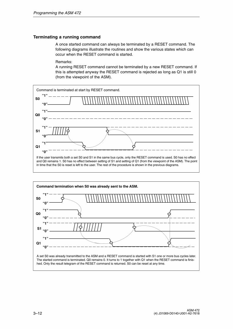
Terminating a running command
A once started command can always be terminated by a RESET command. Thefollowing diagrams illustrate the routines and show the various states which canoccur when the RESET command is started.
Remarks:A running RESET command cannot be terminated by a new RESET command. Ifthis is attempted anyway the RESET command is rejected as long as Q1 is still 0(from the viewpoint of the ASM).
If the user transmits both a set S0 and S1 in the same bus cycle, only the RESET command is used. S0 has no effectand Q0 remains 1. S0 has no effect between setting of S1 and setting of Q1 (from the viewpoint of the ASM). The pointin time that the S0 is reset is left to the user. The rest of the procedure is shown in the previous diagrams.
Command is terminated at start by RESET command.
Q0
S0”1”
“0”
”1”
“0”
Q1
S1”1”
“0”
”1”
“0”
A set S0 was already transmitted to the ASM and a RESET command is started with S1 one or more bus cycles later.The started command is terminated. Q0 remains 0. It turns to 1 together with Q1 when the RESET command is finis-hed. Only the result telegram of the RESET command is returned. S0 can be reset at any time.
Command termination when S0 was already sent to the ASM.
Q0
S0”1”
“0”
”1”
“0”
Q1
S1”1”
“0”
”1”
“0”

Programming the ASM 472
3–13ASM 472 (4) J31069-D0140-U001-A2-7618
3.5 Processing Data Memories
Data memory types
Mobile data memories with various memories are available to the user. Table 3-1lists the various memory capacities available at this time.
Table 3-1 Available memory capacities
Memory Capacity Memory Type MOBY family MDS Type
2 (1,7) Kbytes RAM MOBY I e.g. MDS 302
8 (7) Kbytes EEPROM/FRAM MOBY I e.g. MDS 413E
32 (28) Kbytes FRAM MOBY I e.g. MDS 514
752 bytes EEPROM MOBY E e.g. MDS E600
5 bytes fixed code MOBY F e.g. MDS F125
192 bytes EEPROM, 4 bytes of fixed code
MOBY F e.g. MDS F415
2 Kbytes RAM, 16 bytes OTP MOBY U e.g. MDS U313
32 Kbytes RAM, 16 bytes OTP MOBY U e.g. MDS U524
44 bytes EEPROM MOBY D e.g. MDS D139/I-Code 1
112 bytes EEPROM MOBY D I-Code SLI
256 bytes EEPROM MOBY D Tag-it HF-I
1000 bytes EEPROM MOBY D my-d
20 bytes EEPROM RF300 RF320T
8 Kbytes FRAM RF300 e.g. RF340T
32 Kbytes FRAM RF300 e.g. RF350T
64 Kbytes FRAM RF300 e.g. RF350T (64K)
The values in brackets indicate net capacity with ECC mode.
Addressing
The data memories are addressed linearly from address 0000 to the end address.The ASM 472 automatically recognizes the size of the memory on the MDS. Whenthe end address on the MDS is exceeded, the user receives an error message.
Tables 3-2 and 3-3 show the address space of the individual MDS versions.

Programming the ASM 472
3–14ASM 472
(4) J31069-D0140-U001-A2-7618
Table 3-2 Address space of MDS versions for MOBY I, E, F, U and D
Adressing Hexadecimal Number, 16 Bits Integer Number
Normal With ECC* Normal With ECC*
MOBY I: 2 Kbytes data memory with RAM
Start address
End address
0000
07FC
0000
06F1
+0
+2044
+0
+1777
MOBY I: 8 Kbytes data memory with EEPROM/RAM/FRAM
Start address
End address
0000
1FFC
0000
1BF1
+0
+8188
+0
+7153
MOBY I: 32 Kbytes data memory with RAM/FRAM
Start address
End address
0000
7FFC
0000
6FF1
+0
+32764
+0
+28657
MOBY E: 752 bytes data memory with EEPROM
Start address
End address
0000
02EF
–
–
+0
+751
–
–
ID no.: (fixed-coded; can only be read as a whole)**
Start address
Length
1FF0
0004
–
–
+8176
+4
–
–
MOBY F: MDS F1xx (5 bytes fixed code)
Start address
Length
0000
0005
–
–
+0
+5
–
–
MOBY F: MDS F4xx (192 bytes)
Start address
End address
0040
00FF
–
–
+64
+255
–
–
ID no.: (fixed-coded; can only be read as a whole)**
Start address
Length
0000
0004
–
–
+0
+4
–
–
MOBY U: 2 Kbytes data memory
Start address
End address
0000
07FF
–
–
+0
+2047
–
–
Read OTP memory(write access only possible once) The OTP memory of MOBY U can only be processedcompletely, i.e. the start address must always be specified with value FFF0 hex and thelength with value 10 hex.
Start address
Length
FFF0
10
–
–
–16
+16
–
–
ID no.: (four fixed-coded bytes; can only be read with the MDS status command)

Programming the ASM 472
3–15ASM 472 (4) J31069-D0140-U001-A2-7618
Table 3-2 Address space of MDS versions for MOBY I, E, F, U and D
Adressing Integer NumberHexadecimal Number, 16 BitsAdressing
With ECC*NormalWith ECC*Normal
MOBY U: 32 Kbytes data memory
Start address
End address
0000
7FFF
–
–
+0
+32767
–
–
Read OTP memory (write access only possible once)
Start address
Length
FFF0
10
–
–
–16
+16
–
–
ID no.: (four fixed-coded bytes; can only be read with the MDS status command)
MOBY D: MDS D139 (I-Code 1; 44 bytes)
Start address
End address
0000
002B
–
–
+0
+43
–
–
ID no.: (fixed-coded; can only be read as a whole)
Start address
Length
FFF0
0008
–
–
–16
+8
–
–
MOBY D: ISO-MDS (I-Code SLI; 112 bytes)
Start address
End address
0000
006F
–
–
+0
+111
–
–
ID no.: (fixed-coded; can only be read as a whole)
Start address
Length
FFF0
0008
–
–
–16
+8
–
–
MOBY D: ISO-MDS (Tag-it HF-I; 256 bytes)
Start address
End address
0000
00FF
–
–
+0
+255
–
–
ID no.: (fixed-coded; can only be read as a whole)
Start address
Length
FFF0
0008
–
–
–16
+8
–
–
MOBY D: ISO-MDS (my-d SRF55V10P; 1000 bytes)
Start address
End address
0018
03FF
–
–
+24
+1023
–
–
ID no.: (fixed-coded; can only be read as a whole)
Start address
Length
FFF0
0008
–
–
–16
+8
–
–
* Only MOBY I** The following applies to the data presentation in the process image:
bytes 4 = MSB, bytes 7 = LSB.

Programming the ASM 472
3–16ASM 472
(4) J31069-D0140-U001-A2-7618
Table 3-3 Address space of the transponder versions for RF300
Adressing Hexadecimal Number 16 Bits Integer Number
RF300: 20 bytes data memory (EEPROM)
R/W or OTP memory (EEPROM)(The EEPROM user memory for RF300 can be used either as R/W memory or as an OTPmemory (see RF300 system manual))Start address
End address
FF00
FF13
–256
–237ID no.: (fixed–coded; can only be output as a whole)Start address
Length
FFF0
0008
–16
+8
RF300: 8 Kbytes data memory (FRAM/EEPROM)
R/W or OTP memory (EEPROM)(The EEPROM user memory for RF300 can be used either as R/W memory or as an OTPmemory (see RF300 system manual))Start address
End address
FF00
FF13
–256
–237R/W memory (FRAM)Start address
End address
0000
1FFC
+0
+8188ID no.: (fixed-coded; can only be output as a whole)Start address
Length
FFF0
0008
–16
+8
RF300: 32 Kbytes data memory (FRAM/EEPROM)
R/W or OTP memory (EEPROM)(The EEPROM user memory for RF300 can be used either as R/W memory or as an OTPmemory (see RF300 system manual))Start address
End address
FF00
FF13
–256
–237R/W memory (FRAM)Start address
End address
0000
7FFC
+0
+32764ID no.: (fixed-coded; can only be output as a whole)Start address
Length
FFF0
0008
–16
+8

Programming the ASM 472
3–17ASM 472 (4) J31069-D0140-U001-A2-7618
Table 3-3 Address space of the transponder versions for RF300
Adressing Integer NumberHexadecimal Number 16 Bits
RF300: 64 Kbytes data memory (FRAM/EEPROM)
R/W or OTP memory (EEPROM)(The EEPROM user memory for RF300 can be used either as R/W memory or as an OTPmemory (see RF300 system manual))Start address
End address
FF00
FF13
–256
–237R/W memory (FRAM)Start address
End address
0000
FEFC
+0
–ID no.: (fixed-coded; can only be output as a whole)Start address
Length
FFF0
0008
–16
+8

Programming the ASM 472
3–18ASM 472
(4) J31069-D0140-U001-A2-7618
Initializing data memories
The entire data memory is written with the Init pattern (see chapter 3.2, initializa-tion command).
Required when:
� A new data memory is used which has never been written before.
� After failure or replacement of the battery
� Data memory is to be run in ECC mode (read/write with ECC).
The ASM 472 error ”error in RAM of data memory” (04 HEX) is deleted. Initializa-tion is performed when the initialization command is started (with or without ECC).
The initialization command is not needed during normal operation of a system.
Note
If the memory cannot be initialized, an error message is issued. If the MDS is de-fective, the initialization command is not concluded. Table 3-4 gives you informa-tion on timeout monitoring of the command.

Programming the ASM 472
3–19ASM 472 (4) J31069-D0140-U001-A2-7618
Duration of initialization
After the MDS is in the field of the SLG, initialization is performed in the timeslisted in table 3-4.
Table 3-4 Initialization duration
MDS Type MemorySize
Initialization Duration (inSeconds)
Normal With ECC
1 Kbytes MOBY I: VMDS ASM452 05 00 < 0.1 s –
2 Kbytes MOBY I: RAM 08 00 0.4 s 5 s
8 Kbytes MOBY I: FRAM 20 00 0.8 s 20 s
8 Kbytes MOBY I: EEPROM 20 00 18 s 54 s
32 Kbytes MOBY I: RAM/FRAM 80 00 3 s 75 s
752 bytes MOBY E: EEPROM 02 F0 0.8 s –
192 bytes MOBY F: EEPROM 00 C0 2.2 s –
16 bytes MOBY F: EEPROM 00 10 0.25 s –
2 Kbytes MOBY U: RAM 08 00 Approx. 1 s –
32 Kbytes MOBY U: RAM 80 00 Approx. 1.5 s –
44 bytes MOBY D: MI-Code 1 00 2C
112 bytes MOBY D: ISO I-Code SLI 00 70
256 bytes MOBY D: ISO Tag-it HF-I 01 00
1000 bytes MOBY D: ISO my-d 04 00
64 bytes MOBY D: ISO ST LRI512 00 40
20 bytes RF300: EEPROM 00 14 Approx. 0.2 s –
8 Kbytes RF300: FRAM 20 00 0.3 s –
32 Kbytes RF300: FRAM 80 00 1.2 s –
64 Kbytes RF300: FRAM FF 00 2.4 s –

Programming the ASM 472
3–20ASM 472
(4) J31069-D0140-U001-A2-7618
3.6 Programming New Start and Restart
Startup, PLC
A RESET command must be sent to the ASM 472 when a new start or restart ofthe PLC or the user program occurs.
Startup, ASM 472
A startup of the ASM 472 (e.g., after power failure) is indicated in bit 7 of bytes 0 ofthe acknowledgment telegram. The ERR LED flashes in a 2-second pattern toindicate this condition. The user must now send a RESET command to theASM 472. The flashing stops and the ASM is ready for operation.

4–1ASM 472 (4) J31069-D0140-U001-A2-7618
Sample Applications
Programming of the examples in this chapter has purposely been kept simple. Thischapter gives programmers a quick way to get started. The examples can then beexpanded by the programmer to fit your application requirements.
4

Sample Applications
4–2ASM 472
(4) J31069-D0140-U001-A2-7618
4.1 Programming Example for Allen Bradley
Program description
A MOBY command is started once as soon as an MDS enters the transmissionwindow of an SLG.
Program layout
Figure 4-1 shows the setup of a simple ASM 472 program, embedded in the con-figuration of the RSLogix 500 software. The “LAD2--MAIN” screen shows themain program.
Figure 4-1 Program structure

Sample Applications
4–3ASM 472 (4) J31069-D0140-U001-A2-7618
The individual subprograms are shown on the next few pages.
� M-INIT: One-time initialization of the ASM 472 after the controller is switched on
� M-MAIN: MOBY main program
� M-RESET: Execution of the RESET handshake via control linesS1/Q1
� M-READ: Start read command as soon as an MDS moves into the transmission window. The MOBY commands are output on control lines S0/SQ.
0000SBR
SubroutineSBR
LB3:0
4
M_CMD_START
0001 UB3:0
1
M_WAIT_REQUEST
0002 UB3:0
2
M_WAIT_RESPONSE
0003 UB3:0
5
M_READY
0004 UB3:0
7
M_DATA
0005 UB3:0
6
M_READ_COMMAND
0006 LB3:1
7
M_REBOOT
0007 END
Initialize all MOBY varibles
Figure 4-2 M-INIT

Sample Applications
4–4ASM 472
(4) J31069-D0140-U001-A2-7618
Start RESET command when ASM472 is powered up.
0000SBR
SubroutineSBR I:1
471747–SDN
MOBY_STARTUP
OSRB3:1
8
M_OSR_STARTUP
UB3:0
5
M_READY
LB3:0
4
M_CMD_START
LB3:1
7
M_REBOOT
Call RESET routine
0001B3:1
7
M_REBOOTJSR
Jump To SubroutineSBR File Number U:4
JSR
Start READ command when tag is present.
0002
eeeeeeeeeeeeeeeeeeee
B3:0
5
M_READYI:1
46
MOBY_TAG_PRES
OSRB3:0
12
M_PRESENT
LB3:0
4
M_CMD_START
LB3:0
6
M_READ_COMMAND
UB3:0
7
M_DATA
Call READ routine
0003B3:0
5
M_READYB3:0
6
M_READ_COMMANDJSR
Jump To SubroutineSBR File Number U:9
JSR
Tag data available.––––––Fill in your code for data processing ––––
0004
eeeeeeeeee
B3:0
5
M_READYB3:0
7
M_DATA
UB3:0
6
M_READ_COMMAND
0005 END
Main routine for ASM472 processing
Figure 4-3 M-MAIN

Sample Applications
4–5ASM 472 (4) J31069-D0140-U001-A2-7618
Fill in command code
0000SBR
SubroutineSBR B3:0
4
M_CMD_STARTI:1
451747–SDN
MOBY_Q1MOV
MoveSource 84 48
33<Dest O:1.2
512<
MOVMOBY_OUT
MOVMoveSource 0
0<Dest O:1.3
12<
MOVSDN_COMMAND.3
MOVMoveSource 0
0<Dest O:1.4
513<
MOVSDN_COMMAND.4
Start command with S1
0001B3:0
4
M_CMD_STARTI:1
451747–SDN
MOBY_Q1
LB3:0
1
M_WAIT_REQUEST
UB3:0
2
M_WAIT_RESPONSE
UB3:0
4
M_CMD_START
LO:1
451747–SDN
MOBY_S1
Wait for falling Q1 to reset S1
0002B3:0
1
M_WAIT_REQUESTI:1
451747–SDN
MOBY_Q1
UO:1
451747–SDN
MOBY_S1
LB3:0
2
M_WAIT_RESPONSE
UB3:0
1
M_WAIT_REQUEST
Wait for rising Q1 to reset S1. Command is done
0003B3:0
2
M_WAIT_RESPONSEI:1
451747–SDN
MOBY_Q1
LB3:0
5
M_READY
UB3:1
7
M_REBOOT
0004 END
Perform MOBY I reset command
Figure 4-4 M-RESET

Sample Applications
4–6ASM 472
(4) J31069-D0140-U001-A2-7618
Fill in Command code
0000SBR
SubroutineSBR B3:0
4
M_CMD_STARTMOV
MoveSource 2
512<Dest O:1.2
512<
MOVMOBY_OUT
MOVMoveSource 30 72
12<Dest O:1.3
12<
MOVSDN_COMMAND.3
UB3:0
2
M_WAIT_RESPONSE
Start command. REF–statement is only used for optimization.
0001B3:0
4
M_CMD_START
LO:1
441747–SDN
MOBY_S0
REFRefresh I/OChannel 0 NoChannel 1 No
REF
LB3:0
1
M_WAIT_REQUEST
UB3:0
4
M_CMD_START
Wait for falling Q0 to reset S0.
0002
eeeeeeeeeeeeeeeeeeeee
B3:0
1
M_WAIT_REQUESTI:1
44
MOBY_Q0
UO:1
44
MOBY_S0
REFRefresh I/OChannel 0 NoChannel 1 No
REF
UB3:0
1
M_WAIT_REQUEST
LB3:0
2
M_WAIT_RESPONSE
Wait til MOBY sets the response indicator. Command is done
0003B3:0
2
M_WAIT_RESPONSEI:1
441747–SDN
MOBY_Q0
UB3:0
2
M_WAIT_RESPONSE
LB3:0
7
M_DATA
0004 END
Execute MOBY READ command
Figure 4-5 M-READ

Sample Applications
4–7ASM 472 (4) J31069-D0140-U001-A2-7618
4.2 The ECC Driver
Only MOBY I:The ECC driver (Error Correction Code) can be enabled with the parameterizationof the RESET (see chapter 3.2).
Application
The ECC driver provides an extra guarantee that the data on the MDS are correct.With MDSs with EEPROM the manufacturer only guarantees 10,000 write accesses.The ECC driver gives you the same data security up to the actual end of the MDS’slife.
When security is important, the ECC driver can also be used for MDSs with RAMmemory when extremely strong interference fields may affect communication.
Data correction
If at some point the MDS memory loses 1 bit of data (e.g., with an EEPROM-MDSwhich has been write-accessed very frequently), the ECC driver is able to recon-struct the lost data bit. The user is assured of correct data.
A status bit in the status byte (see chapter 3.3) is available to the user to queryand evaluate the data correction (e.g., to initiate replacement of the ”old” MDS inthe near future).
Function
The ECC driver divides the MDS memory into blocks of 16 bytes. Of these 16 by-tes, 14 are for user data and 2 contain ECC information. Each time the MDS isaccessed, at least one block is read or written (even when the user has only pro-grammed 1 byte). This increases access time to the MDS data. See manual onconfiguration, mounting and service.
When an ECC MDS is read without the ECC driver, the ECC bytes between theuser data can be seen. Writing an ECC MDS without an ECC driver destroys thedata structure of the MDS. The MDS (or the destroyed data block) can no longerbe read with the ECC driver.

Sample Applications
4–8ASM 472
(4) J31069-D0140-U001-A2-7618
Note
� It takes longer to access MDS data (i.e., less data can be processed in dyna-mic operation).
� The net capacity of the MDS decreases (see chapter 3.5).
� When data have to be corrected, the result can be delayed by up to one se-cond.
� A ”normal” MDS must be initialized with enabled ECC driver before being com-missioned (e.g., with the STG I).
Example
A 62-byte MDS has the data structure listed in table 4-1. This information is onlyprovided for explanatory purposes. The programmer and the user do not notice.
Table 4-1 Data structure of a 62-byte MDS
MDS Address fromUser’s Viewpoint
Address on MDS Meaning
01...
13
01...
131415
ECCECC
14 bytes ofuser data 1st block
1415...
27
1617...
293031
ECCECC
14 bytes ofuser data 2nd block
2829...
41
3233...
454647
ECCECC
14 bytes ofuser data 3rd block
48..
61
An incomplete block at the end ofthe MDS memory cannot be usedfor user data.
5–1ASM 472 (4) J31069-D0140-U001-A2-7618
Presence Check
This chapter covers the exact function of the presence check.
5

Presence Check
5–2ASM 472
(4) J31069-D0140-U001-A2-7618
5.1 Definition of Terms
Presence check
The presence check is a piece of recognition logic in the firmware of the ASM 472which is able to tell whether a mobile data memory is present in the surroundingarea of the SLG.
The firmware of the ASM 472 continuously scans its surroundings with the mag-netic field for the presence of a mobile data memory. A hysteresis largely preventsthe presence bit from changing back and forth when a mobile data memory stopson the boundary of the field.
The presence check on the ASM 472 is only enabled when the RESET commandwas parameterized with PRE = 1. With PRE = 0 there is no presence check (seechapter 3.2).
Presence
A mobile data memory is located in the field of influence of the SLG. The presencebit (bit 6 of byte 0 in the acknowledgment telegram) is set.
PRE
Name of the LED on the ASM 472. The PRE LED and bit 6 of byte 0 in the ac-knowledgment telegram both show the presence of an MDS.

Presence Check
5–3ASM 472 (4) J31069-D0140-U001-A2-7618
5.2 Presence Check Switched Off
Description
The magnetic field of the SLG is only turned on when a valid MDS command(read, write, initialize) is started. After a data memory is spotted and the commandis processed, the SLG is turned off again.
This means projects can be implemented in which the distance from SLG to SLGcan be less than specified. Prerequisite is that the adjacent SLG stations are ad-dressed in multiplex mode.
Applications in which large amounts of data must be transmitted during dynamicoperation may require this. Stopping the conveyor belt can be avoided by dividingup the data and distributing the information over several SLGs.

Presence Check
5–4ASM 472
(4) J31069-D0140-U001-A2-7618
5.3 Presence Check Switched On
Description
After a new start or a restart of the automation system (AS) or after a RESET com-mand, the SLG is on and remains active until the AS or the ASM 472 is turned off.
The ASM 472 continuously scans the field around the SLG for the presence of adata memory. When the ASM 472 detects a data memory, PRE = 1 (bit 6 of byte 0in the acknowledgment telegram) is returned to the user during the next bus cycle.Similarly, PRE = 0 is returned when the data memory moves out of the field of theSLG. Figure 5-1 shows how the field is scanned.
When the data memory stops on the boundary of the SLG’s magnetic field, thepresence bit is prevented from permanently switching back and forth by a hystere-sis function which is handled by the processor on the ASM 472.
Read/write commands can be sent to the presence check with complete transpar-ency. Similarly the presence bit retains total validity after a command is started.
MDS
SLG
B
a
bc
L, B: Dimensions of the transmission window of an SLG at a working distance from the MDS (seemanual for configuration, mounting and service ). L = field length. B = field width.
h: Hysteresis: Area in which a presence bit which is once set remains set
Point at which the mobile data memory is detected by the SLG. Starting now the waiting MOBYcommand is processed with the MDS. Presence remains set.
The MOBY must be finished by this time since the data memory is leaving the transmission win-dow. The presence bit still remains set.
Cancel presence in BEST. The MDS has left the transmission window of the SLG. A commandwhich has not yet been processed stops.
Hysteresis field for the presence check
Transmission window: Data communicationbetween MDS and SLG
L
h
h = 0.1 to 15 mm(varies with MDS type)
c
b
a
Figure 5-1 Scanning the field

Presence Check
5–5ASM 472 (4) J31069-D0140-U001-A2-7618
5.4 Startup of the ASM 472
Introduction
The ASM 472 always performs the startup procedure after power-up or after thePLC restarts.
After an extensive self-test, the ASM 472 sends the startup message (bit 7 of byte0 in the acknowledgment telegram). This message shows the user whether theASM 472 is ready for operation (duration of the startup: max. of 3 seconds).
Note
After the startup message, it is mandatory that the user send a RESET commandto the ASM 472.
Startup with presence check on
After the ASM starts up with presence check on, the presence bit is not indicated(PRE = 0) regardless of whether an MDS is in the transmission window. The pres-ence bit does not become valid until a RESET command is concluded positively.
RESET with presence check on
When a RESET command is executed on the ASM 472 while an MDS is located inthe transmission window of the SLG, the presence bit (PRE – see chapter 3.1) dis-appears briefly. After the MDS is detected again, the PRE bit is set again.

Presence Check
5–6ASM 472
(4) J31069-D0140-U001-A2-7618
6–1ASM 472 (4) J31069-D0140-U001-A2-7618
Trouble-Shooting and Error Messages
This chapter gives you information on trouble-shooting. The meaning of the LEDsis described.
In addition the chapter contains a detailed discussion of possible errors and theircauses. Notes on how to correct errors are provided.
6

Trouble-Shooting and Error Messages
6–2ASM 472
(4) J31069-D0140-U001-A2-7618
6.1 Indicator Elements on the ASM 472
The figure below describes the indicator elements of the ASM 472.
ERR
ON (perm.)
OFF
OFF
2 Hz
5 Hz
1 flash every2 sec
PRE
OFF/ON
ON
2 Hz
2 Hz
5 Hz
OFF
LEDs for status of DeviceNetGeneral operating states (SF, BF, ON, 24 V DC) are located on basic module 5136-DNS-200X.
LEDs for MOBYRxD: SLG is active with a command.PRE: Indicates the presence of an MDSERR: Error indicated by flashing pattern (see
table 6-1)The error detected last is alwaysindicated. The error indicator is overwritten by
a new error. The error indicator can be reset with a RESET command.
The PRE and ERR LEDs indicate other operational states of the ASM.
Description, Causes, Remedies
Hardware is defective (RAM, Flash, etc.).
Loader is defective (can only be fixed at the plant).
Firmware load procedure is active or no firmware found.→ Load firmware (see appendix A)→ Do not turn off the ASM while doing this.
Firmware loading terminated with an error.→ New start required→ Load firmware again (see appendix A)→ Check update files
Operating system error→ Turn ASM off and on
ASM has booted and is now waiting for a RESET from theuser.
Figure 6-1 Pin allocation and LEDs of the ASM 472

Trouble-Shooting and Error Messages
6–3ASM 472 (4) J31069-D0140-U001-A2-7618
6.2 General Errors
Program won’t run.
After a new start or a restart, the program won’t run.
Cause:After new start, restart or startup of the ASM 472, no RESET command was exe-cuted. Special handshake bits (S1/Q1, see chapter 3.1) are defined for the RESETcommand.
PLC assumes STOP.
Use the debugging tools of the software manufacturer to localize the error.
Pay particular attention to:
� Address allocation of the ASM 472
� Presence and length of the data blocks
The RESET handshake doesn’t work.
The red error LED on the ASM 472 continues to flash once.
Cause:Communication to the ASM 472 isn’t functioning.
� Check address allocation of the ASM 472.
� Check the entire DeviceNet configuration.

Trouble-Shooting and Error Messages
6–4ASM 472
(4) J31069-D0140-U001-A2-7618
6.3 Evaluating Errors in the Status Byte
If the ASM 472 is not functioning correctly, you can select additional errors by eval-uating the status in the acknowledgment telegram (byte 2 in PII; see chapter 3.1).
The red LED (PRE) flashes to indicate error messages of the ASM 472. The statusbyte contains information in hexadecimal (HEX) format and as fixed point numbers(see table 6-1).
Table 6-1 Error messages of the ASM 472
Status Flashingof Red
LED
Description
00 HEX/00 DEC
- No error
Standard value when everything is okay
1x No error
ASM 472 has executed a startup and is waiting for a RESET ornew start command (see chapter 3.6).
01 HEX/01 DEC
2x Presence error. The MDS moved out of the SLG’s transmissionwindow. The MOBY command was only partially executed.
Read command. No data are supplied to the user.
Write command. The MDS which just left the field contains an in-complete data record.
� Working distance from SLG to MDS was not adhered to.
� Configuration error. The data record to be processed is toolarge (during dynamic operation).
02 HEX/02 DEC
2x Presence error. An MDS moved past an SLG without being pro-cessed by a MOBY command.
Processing error. Command processing of an MDS (read and/orwrite) was not completed.
This error message is not reported immediately. Instead the ASMwaits until the next command (read, write). This command is im-mediately answered with this error. This means that a read or writecommand is not processed. The next command is then executednormally by the ASM.
A RESET also resets this error state.

Trouble-Shooting and Error Messages
6–5ASM 472 (4) J31069-D0140-U001-A2-7618
Table 6-1 Error messages of the ASM 472
Status DescriptionFlashingof Red
LED
03 HEX/03 DEC
3x Error in the connection to the SLG. The SLG doesn’t answer. 24 V power for the SLG is missing.
� Cable between ASM 472 and SLG is wired incorrectly or thereis a cable break.
� 24 V is not connected, is turned off, or has failed briefly. Checkthe various voltages as shown in figure 2-1.
� Electronic fuse on the ASM 472 has blown. Check wiring of theSLG.
� Hardware defective: ASM 472 or SLG
� Another SLG is in the vicinity and is active.
� Interference on SLG or PROFIBUS line
� ASM 472 isn’t parameterized correctly. Compare ”MOBYmode” parameter with the SLG type (see chapter 3.2; RESET command, byte 1)
04 HEX/04 DEC
4x Error in the MDS memory
The MDS has never been written or has lost its contents due tobattery failure.
� Replace MDS (if the battery bit is set).
� Initialize MDS with the STG.
� Process MDS with the INIT command via PLC (see chapter 3.5).
05 HEX/05 DEC
5x Unknown command
The user sent a command to the ASM 472 which cannot be inter-preted.
� The MDS has reported an address error.
� Check MDS address at start of command.
MOBY F:
� Read/write command has password protection.
� FFT command is only permitted with enabled ANW check.
06 HEX/06 DEC
6x Field interference on the SLG
The SLG is receiving interference from its surroundings.
� The distance between two SLGs is too short and does notcomply with the configuration guidelines.
� The connection cable to the SLG is faulty, is too long or doesnot meet specifications.
� MOBY U: The MDS left the field during communication.

Trouble-Shooting and Error Messages
6–6ASM 472
(4) J31069-D0140-U001-A2-7618
Table 6-1 Error messages of the ASM 472
Status DescriptionFlashingof Red
LED
07 HEX/07 DEC
7x Too many sending errors
The MDS was unable to correctly receive the command or thewrite data from the ASM 472 even after several attempts.
� The MDS is positioned directly in the boundary area of thetransmission window.
� The data transmission to the MDS is being affected by extremeinterference.
MOBY F:Another MDS was detected in the field while the command wasbeing processed.
08 HEX/08 DEC
8x CRC sending error
� The monitor receiving circuit detected an error while sending.
– Cause same as for error 06 HEX/06 DEC
� The MDS reports CRC errors very frequently.
– The MDS has stopped on the boundary of the SLG.
– The MDS and/or the SLG have a hardware defect.
09 HEX/09 DEC
9x Only for initialization: CRC error while receiving the acknowledg-ment from the MDS
� Cause same as for error 06 HEX/06 DEC
0A HEX/10 DEC
10x Only for initialization: MDS is unable to execute the initializationcommand.
� MDS is defective.
0B HEX/11 DEC
11x MOBY I: Only for initialization: Timeout while initializing the MDS
� The MDS is positioned directly on the boundary of the trans-mission window.
� The MDS is using too much current (defective).
� MOBY U: MDS memory cannot be read correctly.
0C HEX/12 DEC
12x Memory of the MDS cannot be written.
� Memory of the MDS is defective.
� EEPROM-MDS was written too many times and has now re-ached the end of its life.
0D HEX/13 DEC
13x Address error
� The address area of the MDS was exceeded.
� The start address of the MDS is wrong in the command tele-gram at the start of the command.
– Check bytes 1 and 2 of the command telegram (see chap-ter 3.1).
� MOBY F (MDS F4xx): The start address must be �40H.
� MDS is the wrong type.

Trouble-Shooting and Error Messages
6–7ASM 472 (4) J31069-D0140-U001-A2-7618
Table 6-1 Error messages of the ASM 472
Status DescriptionFlashingof Red
LED
0E HEX/14 DEC
14x ECC error (only possible when the ECC bit is set in the command– see chapter 3.2).
� The data could not be read from the MDS.
� The MDS has lost data (MDS is defective).
� The MDS was not initialized with the ECC driver.
– Initialize MDS.
� MDS with EEPROM has reached the end of its life. The dataare lost.
– Replace MDS.
� The MDS moved out of the field while it was being write-acces-sed.
– The MDS is not positioned correctly.
� Command to ASM issued incorrectly by user.
0F HEX/15 DEC
1x Startup message of ASM. The ASM was off and did not receive aRESET command.
� Perform RESET.
15x Only for MOBY F:
� Internal driver error. Repeat command.
� FFT command was started with MDS F1xx in field.
11 HEX/17 DEC
– – Short circuit or overload of 24 V output to SLG
� The affected output is switched off.
� A reset is only possible by turning the 24 V power off and onagain.
� Then start RESET.
12 HEX/18 DEC
18x Internal ASM communication error
� Hardware of ASM has a defect.
– Return ASM for repairs.
� Start RESET after error is corrected.
13 HEZ/19 DEC
19x Not enough buffer memory on ASM/SLG for intermediate storageof the command
14 HEX/20 DEC
20x Internal ASM error
� Program execution error on ASM
� Turn voltage supply of ASM off and on.
� Start RESET after error is corrected.
15 HEX/21 DEC
21x Incorrect parameterization of ASM
� RESET command is incorrectly parameterized.
� After a startup ASM still has not received a RESET.
16 HEX/22 DEC
22x The FC command cannot be executed with the ASM parameteri-zation on PROFIBUS/DeviceNet.
� FC command (e.g., read) which has too much user data (datalength �12 bytes)

Trouble-Shooting and Error Messages
6–8ASM 472
(4) J31069-D0140-U001-A2-7618
Table 6-1 Error messages of the ASM 472
Status DescriptionFlashingof Red
LED
17 HEX/23 DEC
23x Communication error between application and ASM 472. Handshake error.
� Check command causing this error.
� After the error is corrected, perform RESET command andstart command again.
18 HEX/24 DEC
– – An error has occurred which must be acknowledged with a RE-SET.
� A temporary short circuit has occurred on PROFIBUS/DeviceNet.
� The RESET command is not correct.
� Start RESET command.
19 HEX/25 DEC
– – Previous command is active.
The user sent a new command to the ASM 472 although the lastcommand was still active.
� Active command can only be terminated by RESET.
� Before a new command can be started, handshake bit Q0must be set (see chapter 3.4).
� Then start RESET command.
1A HEX/26 DEC
– – PROFIBUS-DP or DeviceNet error has occurred.
� Bus connection was interrupted.
– Wire break on bus
– Bus plug connector on ASM was pulled briefly.
� BUS-DP master no longer addresses ASM.
� Perform RESET.
� The ASM determined a telegram interruption on the bus. Thebus may have been configured again (e.g., with HW Config).
This error is only indicated when “response monitoring” was ena-bled in the BUS configuration.
1B HEX/27 DEC
27x Only for MOBY F:
� CRC check in data telegram is wrong. Checksum error bet-ween ASM and SLG
� Interface on ASM or SLG is defective.
� Check wiring in ASM-SLG cable.
1C HEX/28 DEC
28x The antenna on the SLG is off. An MDS command to the ASMwas started in this state.
� Turn on the antenna with the command “antenna on/off.”
� The antenna is on (off) but has received an additional “antennaon” (“antenna off”) command.
� MOBY F: An FFT command was started while the antennawas off (SetAnt with mode = 09).

Trouble-Shooting and Error Messages
6–9ASM 472 (4) J31069-D0140-U001-A2-7618
Table 6-1 Error messages of the ASM 472
Status DescriptionFlashingof Red
LED
1D HEX/29 DEC
– – There are more MDSs in the transmission window than the SLGcan process at one time
1F HEX/31 DEC
– – Running command was terminated by RESET or bus connectorwas disconnected.
� Communication with the MDS was terminated by RESET.
� This error can only be returned with a RESET command.

Trouble-Shooting and Error Messages
6–10ASM 472
(4) J31069-D0140-U001-A2-7618
6.4 Pure Hardware Errors
If the ASM 472 is not working correctly but you can’t find any errors in the pro-gram, check the items in table 6-2.
!Caution
When looking for errors which cannot be precisely located, it is essential to adhereto the “5136-DNS-200X DeviceNet Slave Adapter” user’s guide.
Table 6-2 Pure hardware errors
Error Cause
Power supply Measure 24 V under load!
Wiring of ground Check wiring. See installation guidelines inthe manual for configuration, mounting andservice. Otherwise the wiring guidelines forSIMATIC apply.
Shielding Apply shield. Adhere to manual for configu-ration, mounting and service.
Cable. See manual for configuration, moun-ting and service.
� Correct cable to the SLG used?
� Check cable length (adhere to cableconfiguration!).
Wiring � Plugs of SLG and ASM 472 okay?
� Are distributor sockets installed in theconnection?
Mounting � Make sure space is free of iron. See in-stallation guidelines in the manual onconfiguration, mounting and service.
� Adhere to working distances. See tech-nical data in the manual on configura-tion, mounting and service.
� Adhere to minimum distances. See tech-nical data in the manual on configura-tion, mounting and service.
– MDS � MDS;
– SLG � SLG
� Is the guide of the MDS within the speci-fied transmission window?

7–1ASM 472 (4) J31069-D0140-U001-A2-7618
Technical Data of the ASM 472
Table 7-1 Technical data
ASM type for identification system ASM 472MOBY I/E/F/U/D and RF300
Interface to 5136-DNS-200X SIMATIC P busCyclic process image
Serial interface to SLG
Plug connector 2 M12 coupling plugs
Line length 2 m = standard length. Other fabricated cables= 5 m, 10 m, 20 m, 50 m (up to 1000 m for cu-stomer’s own cable fabrication)
SLGs which can be connected 1 SLG 4x, SLG 7x or SLG 8x
Software functions
Programming Depends on DeviceNet scanner
Function blocks None
– GE 90/30 and GE 90/70 Sample programs
MDS addressing Direct access with addresses
Commands Initialize MDS, read data from MDS, write datato MDS, turn antenna on/off
MOBY I dialog: Normal station/VMDS
Yes/no
Diagnosis via DeviceNet No
S7 diagnosis No
Firmware can be loaded Yes, but only with SIMATIC S7 tools
Voltage
Nominal value 24 V DC
Permissible range 20.4 V to 28.8 V DC
Current consumption
– From encoder voltage 75 mA (typical)
– From load voltage (SLG power) Max. of 500 mA. Current value: See technicaldata of the connected SLG.
Power loss of the module 1.6 W (typical)
Digital inputs Via expansion modules from the ET 200X fa-mily
Digital outputs Via expansion modules from the ET 200X fa-mily
7

Technical Data of the ASM 472
7–2ASM 472
(4) J31069-D0140-U001-A2-7618
Table 7-1 Technical data
Ambient temperature
Operation 0 °C to +55 °C
Transportation and storage -40 °C to +70 °C
Dimensions (W x H x D) in mm
Dimensions of single device 87 x 110 x 55
Scaling dimensions 60 x 110 x 55
Mounting 2 M5 screws
Protection rating IP 67
Information on setup and other general technical data are available in the ET 200Xmanual or the user’s guide “5136-DNS-200X DeviceNet Slave Adapter.”
Table 7-2 MOBY times with presence check
MDS is detected. No command active.(Presence 0 � 1)
70 msec (typical)
MDS moves away (presence 1 � 0) 110 msec (typical)
MDS is detected. Command on ASM 472 active. (Pre-sence 0 � 1)
20 msec (typical)
Return message of SLG after command starts 10 to 100 msec

Technical Data of the ASM 472
7–3ASM 472 (4) J31069-D0140-U001-A2-7618
Transmission times to the MDS
Communication between ASM and MDS is described in chapter 3.1.3 of themanual for configuration, mounting and service. The cycle time of the PLC mustalso be considered when calculating the total time from command start to result.The user sees this time when he/she starts a command while an MDS is alreadylocated in the transmission window of the SLG. Table 7-3 provides the total trans-mission times.
Table 7-3 Transmission times to the MDS (MOBY I)
Transmission Time
Transmission time for one command when cycle time of PLC> 12 msec
3 cycles 2
Transmission time for one command when cycle time of PLC< 12 msec
(K+tByte�n)1 + 2 cycles
Average value for read/write 255 bytes (cycle time = 16 msec.22 commands are sent to the ASM.)
1300/1700 msecWithout/with refresh
Average value for read/write 255 bytes (cycle time = 4.5msec. 22 commands are sent to the ASM.)
1000 msecWithout/with refresh
1 For formula cf. manual for configuration, mounting and service, chapter 3.1.3. The followingapplies for RAM-MDS data with length of 12 bytes: 16 msec + 0.8 msec�12 bytes.
2 Only applies to a block length � 12 bytesThe following applies to longer block lengths: 3 cycles for each 12-byte block started.

Technical Data of the ASM 472
7–4ASM 472
(4) J31069-D0140-U001-A2-7618

A–1ASM 472 (4) J31069-D0140-U001-A2-7618
Firmware Update
The ASM 472 has a flash memory for the loadability of the firmware. Under certainconditions a firmware update can sometimes be performed at the customer’s. Thischapter describes how to do this.
A

Firmware Update
A–2ASM 472
(4) J31069-D0140-U001-A2-7618
System prerequisites� SIMATIC S7-300 with PROFIBUS connection
� ET 200X basis station, type BM 141, BM 142 or BM 143
� SIMATIC software, at least STEP 7 V5.1 service pack 1
� MOBY software, at least V3.2
� Programmer (PG or PC)
How to proceed� In HW Config of SIMATIC Manager, place an ASM 473 (6GT2 002-0HA00) so
that it looks like the figure below.
Figure A-1 Placing an ASM 473
� Assemble the hardware and wire PROFIBUS. The ASM 472 which is to receivean update is now installed in place of the ASM 473.

Firmware Update
A–3ASM 472 (4) J31069-D0140-U001-A2-7618
� The firmware update can now be called with the object properties of the ASM473.
Figure A-2 Calling the firmware update

Firmware Update
A–4ASM 472
(4) J31069-D0140-U001-A2-7618

B–1ASM 472 (4) J31069-D0140-U001-A2-7618
Warnings
Hazardous voltages are present in this equipment during operation.
To ensure safe operation of the equipment, maintenance shall only beperformed by qualified personnel in accordance with the instructionsin the MOBY catalog1 and technical description.
Failure to observe these instructions can result in death, severe perso-nal injury or substantial damage to property.
The following instructions and those on all product labels must befollowed when carrying out any maintenance work.
� Always disconnect and earth the equipment before startingany maintenance.
� Use only spare parts authorized by the manufacturer.
� The servicing intervals as well as the instructions for repairand replacement shall be duly observed.
� A lithium battery is contained in mobile data memories withRAM. The following instructions must be observed:
To avoid the risk of fire, explosion and severe burns, the bat-tery should not be recharged, dismantled, exposed to heatover 100 degrees Celsius, ignited, or brought into contactwith water.
The special instructions must be followed when using heat-resistantdata storage media.1 Should you not be in possession of the MOBY catalog, it can be
obtained through your local Siemens office.
Warning
English
!Beim Betrieb elektrischer Geräte stehen zwangsläufig bestimmteTeile dieser Geräte unter gefährlicher Spannung.
Sicherer Betrieb der Geräte setzt voraus, dass diese von qualifizier-tem Personal sachgemäß unter Beachtung der im MOBY-Katalog1
und der technischen Beschreibung enthaltenen Hinweise eingesetztwerden.
Bei Nichtbeachtung können Tod, schwere Körperverletzung oder er-heblicher Sachschaden die Folge sein.
Beachten Sie daher auch bei Instandhaltungsmaßnahmen an diesemGerät alle hier und auf dem Produkt selbst aufgeführten Hinweise.
� Vor Beginn jeglicher Arbeiten ist das Gerät vom Netz zu tren-nen und zu erden.
� Es dürfen nur vom Hersteller zugelassene Ersatzteile verwen-det werden.
� Die vorgeschriebenen Wartungsintervalle sowie die Anwei-sungen für Reparatur und Austausch sind unbedingt einzuhal-ten.
� Bei einem mobilen Datenspeicher mit RAM ist eine Lithium-batterie integriert, hierzu sind folgende Hinweise zu beachten:
Vermeiden Sie das Risiko von Feuer, Explosionen und schwe-ren Verbrennungen. Die Batterie darf nicht nachgeladen, aus-einandergebaut, über 100� Celsius erwärmt, entzündet oderihr Inhalt mit Wasser in Berührung gebracht werden.
Beim hitzefesten Datenträger sind die besonderen Hinweise zu be-rücksichtigen.1 Sollten Sie nicht im Besitz des MOBY-Katalogs sein, so kann er
über jede örtliche SIEMENS-Niederlassung bestellt werden.
Deutsch
Warnung!
B

Warnings
B–2ASM 472
(4) J31069-D0140-U001-A2-7618
Français Italiano
Le fonctionnement d’un équipement électrique implique nécessairement laprésence de tensions dangereuses sur certaines de ses parties.
L’exploitation sûre de cet équipement implique qu’il soit mis en oeuvre defaçon adéquate par des personnes qualifiées, en respectant les consignes desécurité figurant au catalogue MOBY1 et aux descriptions techniques.
Le non-respect des consignes de sécurité peut conduire à la mort, à deslésions corporelles graves ou à un dommage matériel important.
Ne procéder à l’entretien que dans le plus grand respect des règles de sécu-rité énoncées ici ou figurant sur le produit.
� Avant toute intervention, mettre l’appareil hors tension et à la terre.
� N’utiliser que des pièces de rechange autorisées.
� Respecter la périodicité d’entretien et les instructions de réparationet de remplacement.
� Les mémoires embarquées (RAM) sont équipées d’une pile au li-thium.
Ne pas exposer la pile au feu, danger d’explosion et de lésions gra-ves. La pile ne doit pas être rechargée, ouverte exposée à destempératures supérieures à 100� C ou exposée au feu. Son contenune doit pas entrer en contact avec de l’eau.
En ce qui concerne les supports de données résistants à la chaleur, respecterles consignes spécifiques.1 Si vous ne disposez pas ou du catalogue MOBY, ce peuvent être com-
mandés auprès de votre agence SIEMENS.
Attention Pericolo
Durante il funzionamento di apparecchi elettrici, determinate parti di taliapparecchi si trovano inevitabilmente sotto tensione pericolosa.
Per un funzionamento sicuro di questi apparecchi è necessario che essivengano adoperati, nel modo opportuno, solo da personale qualificato,che osservi le indicazioni contenute nel catalogo1 per gli apparecchiMOBY e nella descrizione tecnica.
In caso di non osservanza si possono verificare la morte, gravi lesioni allepersone o notevoli vanni alle cose.
Per questo motivo è necessario che le avvertenze riportate qui e sul pro-dotto stesso vengano rispettate anche nel caso di misure di manutenzionedegli apparecchi.
� Prima di iniziare qualsiasi lavoro è necessario staccare l’apparec-chio dalla rete ed effettuare una messa a terra.
� Possono essere utilizzati solo pezzi di ricambio prodotti dal cos-truttore.
� E’assolutamente necessario rispettare i tempi di manutenzioneprevisti e le indicazioni riguardanti il ricambio e la riparazione.
� In una memoria dati mobile dotata di RAM è integrata una batte-ria al litio; in questo caso è necessario osservare le seguenti indi-cazioni:
evitare il pericolo di incendio, di esplosioni e di gravi ustioni.E’vietato ricaricare, smontare, riscaldare oltre i 100��C o incen-diare la batteria, oppure mettere il suo contenuto a contatto conacqua.
Nel caso di un supporto dati resistente al calore è necessario osservare leindicazioni speciali al riguardo.1 Se non doveste essere in possesso del catalogo MOBY, potete ordi-
narlo presso qualsiasi filiale SIEMENS di zona.
Español Svensk
PrecauciónDurante el funcionamiento de los equipos eléctricos hay partes de los mis-mos que se encuentran forzosamente bajo tensión peligrosa.
Un funcionamiento seguro de los equipos presupone que han sido instala-dos correctamente por personal calificado observando las indicacionescontenidas en el Catálogo1 de los equipos MOBY y la Descripción técnica.
La no observación de dichas indicaciones puede provocar la muerte, lesio-nes corporales graves o daños materiales considerables.
Por este motivo es preciso observar también durante las operaciones demantenimiento y reparación en dicho equipo todas las indicaciones que fi-guran aquí y en el producto.
� Antes de comenzar cualquier trabajo es preciso seccionar de la redel equipo y ponerlo a tierra.
� Solo deben utilizarse repuestos homologados por el fabricante.
� Es imprescindible observar los intervalos de mantenimiento especi-ficados asi como las instrucciones de reparación y reemplazo.
� Las memorias de datos móviles con RAM tienen integrada unabatería de litio; al respecto es preciso observar las indicacionessiguientes:
Evite riesgos de fuego, explosiones y quemaduras graves. La ba-tería no debe ser recargada, desmontada, calentada a mas de 100grados centígrados, inflamada: su contenido no deberá ponerse encontacto con agua.
En los soportes de datos con protección térmica es preciso observar las in-dicaciones particulares respectivas.1 Si no dispone del catálogo MOBY, estos pueden pedirse a través de
cualquier sucursal local de SIEMENS.
VarningVid drift av elektrisk utrustning ligger det alltid en farlig spänning på vissadelar av utrustningen.
Säker drift av utrustningen förutsätter att den utförs av kvalificerad perso-nal med uppmärksamhet på anvisningarna i MOBY-katalogen1 samt deanvisningarsom ges i den tekniska beskrivningen.
Om dessa anvisningar ej beaktas kan följden bli dödsfall, svår kroppskadaeller avsevärda materielskador.
Uppmärksamma vid underhållsarbete också anvisningar som ges här ochpå själva produkten.
� Före allt arbete skall utrustningen skiljas fran nätet och jordas.
� Bara reservdelar som godkänts av tillverkaren får användas.
� lakttag alltid föreskrivna underhållsintervall samt de anvisningarsom givits rörande reparation och utbyte.
� Det mobila dataminnet med RAM innehåller et litiumbatteri. Fördetta gäller följande anvisningar:
Undvik risk för öppen låga, explosioner och förbränning. Batterietfår inte efterladdas, tas isär, värmas upp över 100� C eller tändaspå., och dess innehåll får ej komma i beröring med vatten.
För värmebeständiga datamedier gäller speciella anvisningar, som måstebeaktas.1 Om Ni inte har ett exemplar av MOBY-katalogen så kan den bestållas
från närmaste SIEMENS-kontor.
! !
! !