mobile phone charger report
TRANSCRIPT

8/6/2019 Mobile Phone Charger Report
http://slidepdf.com/reader/full/mobile-phone-charger-report 1/16
1
Project Report Mobile Phone Charger

8/6/2019 Mobile Phone Charger Report
http://slidepdf.com/reader/full/mobile-phone-charger-report 2/16

8/6/2019 Mobile Phone Charger Report
http://slidepdf.com/reader/full/mobile-phone-charger-report 3/16
3
Con te n t
System Overview...............................................3System Requireme n ts a nd Specificati on s............6Operati on al Sce n ari o ..........................................7System Perf o rma n ce..........................................8Perf o rma n ce A n alysis ......................................13So ftware Cod e..................................................14Con clusi on ........................................................15Refere n ce.........................................................17
8/6/2019 Mobile Phone Charger Report
http://slidepdf.com/reader/full/mobile-phone-charger-report 4/16

8/6/2019 Mobile Phone Charger Report
http://slidepdf.com/reader/full/mobile-phone-charger-report 5/16
5
Figure 3. Hardware overview of the whole buck converter circuitry system
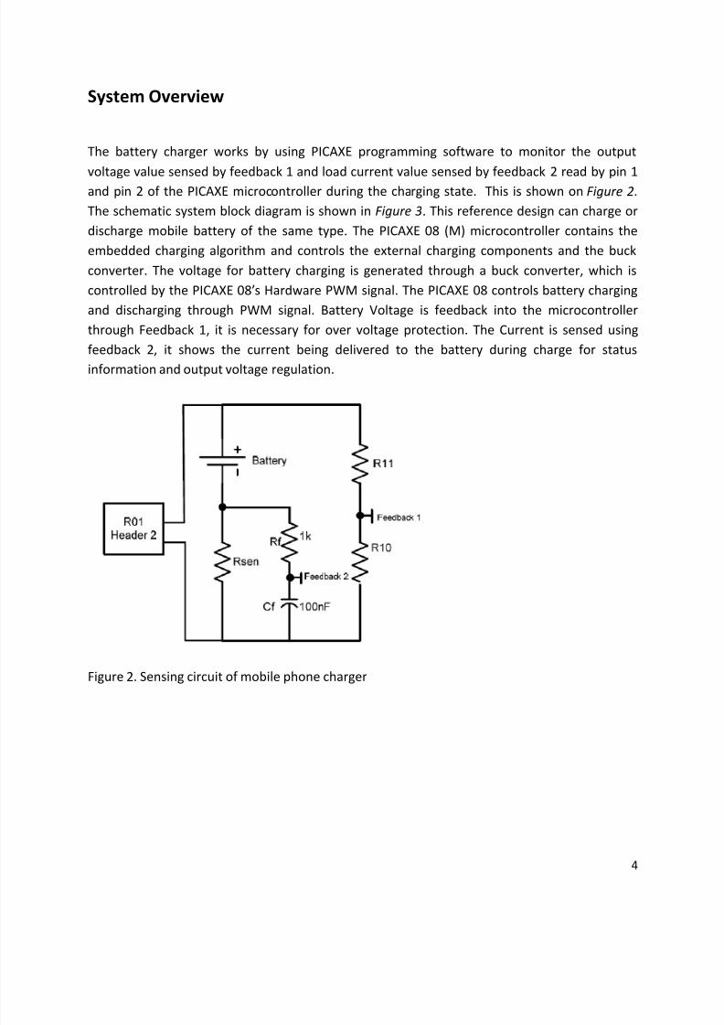
From Figure 3 the PICAXE 08 M is used to generate a sequence of 5 V PWM (Pulse-Width-
Modulation) signal out of pin2
, sending the required duty cycle into the gate-source terminalsof the MOSFET 2N7000 switch. Q1 2N7000 boost the PWM signal to a 1 2 V pulse which thesignal is further boosted by the IR 2 11 7 driver to with its R1, R 2 and D 2 components in order todrive the switch Q 2 which controls the output voltage connected to the load R 0 1 of the buckconverter . Only one converter is used for the mobile phone charger application.

8/6/2019 Mobile Phone Charger Report
http://slidepdf.com/reader/full/mobile-phone-charger-report 6/16
8/6/2019 Mobile Phone Charger Report
http://slidepdf.com/reader/full/mobile-phone-charger-report 7/16
7
Operati on al Sce n ari o
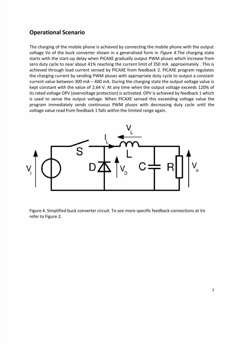
The charging of the mobile phone is achieved by connecting the mobile phone with the outputvoltage Vo of the buck converter shown in a generalised form in Figure 4 .The charging state
starts with the start-up delay when PICAXE gradually output PWM pluses which increase fromzero duty cycle to near about 4 1% reaching the current limit of 3 5 0 mA approximately . This isachieved through load current sensed by PICAXE from feedback 2 . PICAXE program regulatesthe charging current by sending PWM pluses with appropriate duty cycle to output a constantcurrent value between 3 00 mA 400 mA. During the charging state the output voltage value iskept constant with the value of 2 .6 4 V. At any time when the output voltage exceeds 1 20% of its rated voltage OPV (overvoltage protection) is activated. OPV is achieved by feedback 1 whichis used to sense the output voltage. When PICAXE sensed this exceeding voltage value theprogram immediately sends continuous PWM pluses with decreasing duty cycle until thevoltage value read from feedback 1 falls within the limited range again.
Figure 4 . Simplified buck converter circuit. To see more specific feedback connections at Vorefer to Figure 2 .

8/6/2019 Mobile Phone Charger Report
http://slidepdf.com/reader/full/mobile-phone-charger-report 8/16
8
System Perf o rma n ce
PICAXE PWM Output 5 VVoltage across D3 1 2 VVo (output voltage) 2 .6 4 V (across dummy load)IL (output current) 33 7 mA (across dummy load)V (voltage ripple) 1 00 mVI (current ripple) 6 0 mADummy load is Resistor R = 8 .2 ohmCapture d Wavef o rms:
Figure 5. PI CAXE PWM Output = 5v

8/6/2019 Mobile Phone Charger Report
http://slidepdf.com/reader/full/mobile-phone-charger-report 9/16
9
Figure 6. V o ltage acr o ss D3 = 12 V
Figure 7. V o (o utput v o ltage) = 2.64 V

8/6/2019 Mobile Phone Charger Report
http://slidepdf.com/reader/full/mobile-phone-charger-report 10/16
10
Figure 8. V = 100 mV
Figure 9. I = 60 mA
8/6/2019 Mobile Phone Charger Report
http://slidepdf.com/reader/full/mobile-phone-charger-report 11/16
11
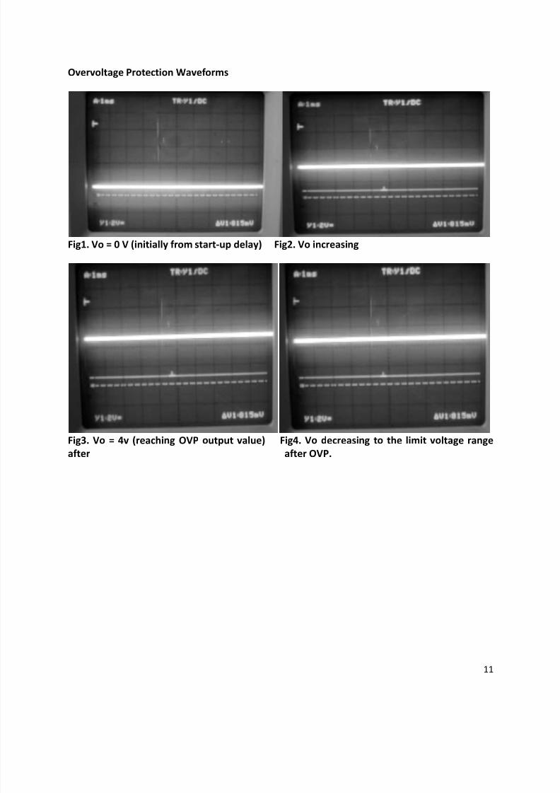
Overv o ltage Pr o tecti on Wavef o rms
Fig1. Vo = 0 V (in itially fr o m start-up d elay) Fig2. V o in creasi n g
Fig3. Vo = 4v (reachi n g OVP o utput value) Fig4. V o d ecreasi n g t o the limit v o ltage ra n geafter after OVP.

8/6/2019 Mobile Phone Charger Report
http://slidepdf.com/reader/full/mobile-phone-charger-report 12/16
12

8/6/2019 Mobile Phone Charger Report
http://slidepdf.com/reader/full/mobile-phone-charger-report 13/16
13
Perf o rma n ce A n alysis
The waveforms illustrate the dc dc converter output response for a current step from zerocurrent to Io. The response of the buck converter changes depending on the current at theoutput. The response time for the current to increase and reach the stable value is about 0 .5 seconds. All waveforms are taken across the dummy load (Resistor of 8 .2 ohm).We are controlling the voltage using the current so the microcontroller is programmed tocontrol the current. The waveforms are little bit noisy. To reduce the current ripple to about40 mA, Rf and Cf are used to be about 1k and 1 00 nF.
We got efficiency ranging between 5 2 and 5 8 % .
Efficie n cy:
= 2 .6 4 * 0 .33 4 / (1 2 * 0 .13 4 )
= 5 4 .8 %
Efficiency Factors:
Conduction losses that depend on load:
y Resistance when the transistor or MOSFET switch is conducting.y Diode forward voltage drop (usually 0 .7 V )y Inductor winding resistancey Capacitor equivalent series resistance
Switching losses:
y Voltage-Ampere overlap lossy Frequency switch *CV2 loss

8/6/2019 Mobile Phone Charger Report
http://slidepdf.com/reader/full/mobile-phone-charger-report 14/16
14
Con clusi on
This project has given a basic insight in to the working of a buck converter. It is seen that if rippleincreases, then the efficiency decreases. An optimum switching frequency and inductor currentripple pair is important as it maximizes the efficiency of a buck converter. We have generatedthe voltage and current depending on the specifications given. If high efficiency is the mostimportant parameter to achieve, then a low switching frequency is the best choice. As differentmobile takes in different voltage input, so current sensing is used to limit the duty cycle.
8/6/2019 Mobile Phone Charger Report
http://slidepdf.com/reader/full/mobile-phone-charger-report 15/16
15
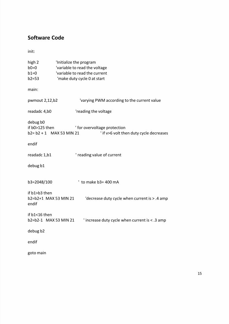
So ftware Cod e
init:
high 2 'Initialize the programb0 =0 'variable to read the voltageb1= 0 'variable to read the currentb2 =5 3 'make duty cycle 0 at start
main:
pwmout 2 ,12 ,b2 'varying PWM according to the current value
readadc 4 ,b 0 'reading the voltage
debug b 0 if b0> 12 5 then ' for overvoltage protectionb2 = b2 + 1 MAX 5 3 MIN 2 1 ' if v > 6 volt then duty cycle decreases
endif
readadc 1,b1 ' reading value of current
debug b1
b3= 2048 /1 00 ' to make b3= 400 mA
if b1 > b3 thenb2 =b2 +1 MAX 5 3 MIN 2 1 'decrease duty cycle when current is > .4 ampendif
if b1<1 6 thenb2 =b2 -1 MAX 5 3 MIN 2 1 ' increase duty cycle when current is < .3 amp
debug b 2
endif
goto main

8/6/2019 Mobile Phone Charger Report
http://slidepdf.com/reader/full/mobile-phone-charger-report 16/16
16
Refere n ces
Papers
[1] Jinwen Xiao, Angel Peterchev, Jianhui, Seth Sanders, An Ultra-Low-Power Digitally-Controlled Buck Converter IC for Cellular Phone Applications , Applied Power ElectronicsConference and Exposition, 2004 . N ineteenth Annual IEEE, Volume 1, Issue, 2004 Page(s):38 3 - 3 9 1 Vol.1[2 ] Michael D. Mulligan, Bill Broach, and Thomas H. Lee, A Constant- Frequency Method forImproving Light-Load Efficiency in Synchronous Buck Converters , Power Electronics Letters,IEEE Volume 3, Issue 1, March 200 5