mo january 2014
DESCRIPTION
hhhTRANSCRIPT

2D NanomaterialsDOI: 10.1002/anie.201309474
Patternable Large-Scale Molybdenium Disulfide Atomic LayersGrown by Gold-Assisted Chemical Vapor Deposition**Intek Song, Chibeom Park, Misun Hong, Jaeyoon Baik, Hyun-Joon Shin, and Hee Cheul Choi*
Abstract: A novel way to grow MoS2 on a large scale withuniformity and in desired patterns is developed. We use Au filmas a catalyst on which [Mo(CO)6] vapor decomposes to forma Mo-Au surface alloy that is an ideal Mo reservoir for thegrowth of atomic layers of MoS2. Upon exposure to H2S, thissurface alloy transforms into a few layers of MoS2, which canbe isolated and transferred on an arbitrary substrate. By simplypatterning Au catalyst film by conventional lithographictechniques, MoS2 atomic layers in desired patterns can befabricated.
Two-dimensional (2D) MoS2 has gained much attention forits intrinsically semiconducting property that is absent ingraphene.[1–5] To fully exploit such an advantage in variousapplications, it is required to secure uniform, large-scale, andpatterned atomic layers of MoS2. The patternability of MoS2
is of special interest for the fabrication of MoS2 atomic layersinto complex hybrid heterostructures composed with differ-ent kinds of 2D nanomaterials.[6, 7] As a consequence, therehas been a rapid increase in the number of reports regardinglarge-scale synthesis of MoS2 by chemical vapor deposition(CVD).[8–12] However, none of these syntheses has accom-plished all of the properties of uniformity, scalability, andpatternability owing to their intrinsic limitations.[13] Amongthese, the preparation of an atom-thick and uniform Mo layerover a wide area of a substrate, that is, a large-scale Moreservoir, is currently the most difficult hurdle to overcome.
Herein, we report a novel way to prepare transferablefew-layer MoS2 structures in desired sizes and patterns with
high uniformity by a gold catalyst-assisted CVD process. Ourfinding encompasses the following: 1) The Mo-Au surfacealloy is readily formed by the low-temperature reaction of[Mo(CO)6] and pre-deposited Au thin film, which acts asa large-scale Mo reservoir; 2) large-scale MoS2 atomic layersare successfully grown upon the subsequent reaction of theMo-Au surface alloy with H2S; 3) the resulting MoS2 atomiclayers are easily isolated from the substrate by etching Aulayers; and 4) atomic layers of MoS2 can be grown in specificpatterns by simply defining the pattern of Au thin film.
Scheme 1 shows a flow chart to acquire large-scale andpatterned MoS2 atomic layers through the formation ofa uniform Mo precursor reservoir by a Mo-Au alloy on a Authin film. The formation of Mo-Au alloy, the key step toacquire a uniform and patternable Mo reservoir, is predictedfrom their phase diagram (Supporting Information, Fig-ure S1).[14] For this, the Au film pre-deposited on a Si substratewas reacted with 0.1 atm of [Mo(CO)6] vapor followed by thereaction with H2S at 300 8C under atmospheric pressure forsulfidation (Supporting Information, Figure S2a).[15] Thesample shows no significant change of color (Figure 1a).
Scheme 1. CVD treatment of [Mo(CO)6] on Au thin film forms a Mo-Ausurface alloy, which further reacts with H2S to form MoS2 atomic layersin large scale (a) and in a specific pattern (b). The as-grown MoS2
atomic layers are easily removed from the Mo-Au alloy substrate andtransferred to arbitrary substrates.
[*] I. Song, C. Park, M. Hong, H. C. ChoiCenter for Artificial Low Dimensional Electronic SystemsInstitute for Basic Science (IBS)77 Cheongam-Ro, Nam-Gu, Pohang, 790-784 (Korea)
I. Song, C. Park, M. Hong, H. C. ChoiDepartment of ChemistryPohang University of Science and Technology (POSTECH)77 Cheongam-Ro, Nam-Gu, Pohang, 790-784 (Korea)E-mail: [email protected]: http://www.postech.ac.kr/chem/nmrl
J. Baik, H.-J. ShinPohang Accelerator Laboratory and Department of PhysicsPohang University of Science and Technology (POSTECH)77 Cheongam-Ro, Nam-Gu, Pohang, 790-784 (Korea)
[**] This work was partially supported by the National ResearchFoundation of Korea (NRF) grant (2010-00285,2012R1A2A1A01003040, and 2009-0094036). I. Song is grateful toGlobal Ph.D. Fellowship grant from NRF (2012H1A2A1016525). Wethank Pohang Accelerator Laboratory (Beamline 8A1).
Supporting information for this article is available on the WWWunder http://dx.doi.org/10.1002/anie.201309474.
.AngewandteCommunications
1266 � 2014 Wiley-VCH Verlag GmbH & Co. KGaA, Weinheim Angew. Chem. Int. Ed. 2014, 53, 1266 –1269
Note that high-quality MoS2 atomic layers are occasionallyobtained at this stage (Supporting Information, Figure S3).The sample was then etched with Au etchant and transferredto a SiO2 substrate (Supporting Information, Figure S2b).Further reaction with H2S at 800 8C enhances crystallinity andcompletes sulfidation (Supporting Information, Figure S2c).
A representative bright-field optical image of a final pieceof MoS2 atomic layers (2 � 2 cm2) transferred on a SiO2/Sisubstrate is shown in Figure 1b. The size and shape of thetransferred MoS2 layers are very well matched with those ofAu film. The homogeneous color contrast induced by MoS2
layers on a SiO2/Si substrate implies that the as-grown MoS2 isfairly uniform in thickness.
The successful formation of MoS2 in atomic layers wasinitially characterized by Raman spectroscopy. A representa-tive Raman spectrum of MoS2 shows two characteristic peaksof E1
2g and A1g at 385.3 and 405.6 cm�1, respectively (Fig-ure 1c). The Raman spectra taken at seven different locationsinside the sample (Figure 1d) and at the edge of the sample(Supporting Information, Figure S4) show comparable peakpositions. This result supports the notion that the product isuniform over the large area. Furthermore, the energy differ-ence of 20.3 cm�1 between E1
2g and A1g peaks suggest that thenumber of MoS2 layers is two.[16] This inference is wellsupported by AFM results (Figure 1 e) showing that the
height of MoS2 layers placed on a SiO2/Si substrate is 1.6 nm,which matches to the height of two to three layers of MoS2.
X-ray photoelectron spectroscopy (XPS) studies con-firmed the chemical identity of MoS2. The high-resolutionspectrum of Mo3d shows that there are two strong peaks at232.6 eV (3d3/2, blue) and 229.5 eV (3d5/2, green) with oneweak peak at 226.5 eV (S 2s, orange), all of which aredeconvoluted into single Gaussian–Lorentzian curves (Fig-ure 1 f). The absence of peaks near 236 eV rules out thepresence of Mo6+ and thus that of MoS3. The S 2p spectrumclarifies that the oxidation state of S is �2 (SupportingInformation, inset in Figure S5). Note that the presence ofoxides is ruled out, as the O1s spectrum only shows thepresence SiO2, not metal oxide peaks.
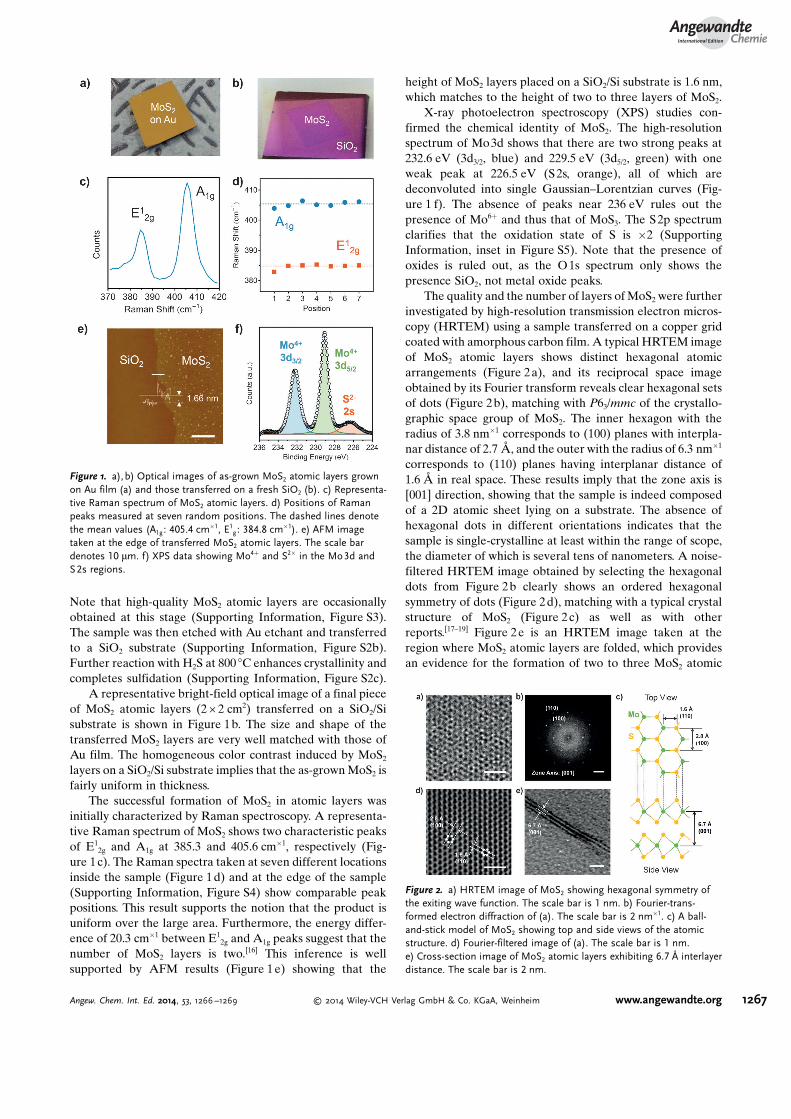
The quality and the number of layers of MoS2 were furtherinvestigated by high-resolution transmission electron micros-copy (HRTEM) using a sample transferred on a copper gridcoated with amorphous carbon film. A typical HRTEM imageof MoS2 atomic layers shows distinct hexagonal atomicarrangements (Figure 2a), and its reciprocal space imageobtained by its Fourier transform reveals clear hexagonal setsof dots (Figure 2b), matching with P63/mmc of the crystallo-graphic space group of MoS2. The inner hexagon with theradius of 3.8 nm�1 corresponds to (100) planes with interpla-nar distance of 2.7 �, and the outer with the radius of 6.3 nm�1
corresponds to (110) planes having interplanar distance of1.6 � in real space. These results imply that the zone axis is[001] direction, showing that the sample is indeed composedof a 2D atomic sheet lying on a substrate. The absence ofhexagonal dots in different orientations indicates that thesample is single-crystalline at least within the range of scope,the diameter of which is several tens of nanometers. A noise-filtered HRTEM image obtained by selecting the hexagonaldots from Figure 2b clearly shows an ordered hexagonalsymmetry of dots (Figure 2d), matching with a typical crystalstructure of MoS2 (Figure 2 c) as well as with otherreports.[17–19] Figure 2e is an HRTEM image taken at theregion where MoS2 atomic layers are folded, which providesan evidence for the formation of two to three MoS2 atomic
Figure 1. a), b) Optical images of as-grown MoS2 atomic layers grownon Au film (a) and those transferred on a fresh SiO2 (b). c) Representa-tive Raman spectrum of MoS2 atomic layers. d) Positions of Ramanpeaks measured at seven random positions. The dashed lines denotethe mean values (A1g: 405.4 cm�1, E1
g: 384.8 cm�1). e) AFM imagetaken at the edge of transferred MoS2 atomic layers. The scale bardenotes 10 mm. f) XPS data showing Mo4+ and S2� in the Mo3d andS2s regions.
Figure 2. a) HRTEM image of MoS2 showing hexagonal symmetry ofthe exiting wave function. The scale bar is 1 nm. b) Fourier-trans-formed electron diffraction of (a). The scale bar is 2 nm�1. c) A ball-and-stick model of MoS2 showing top and side views of the atomicstructure. d) Fourier-filtered image of (a). The scale bar is 1 nm.e) Cross-section image of MoS2 atomic layers exhibiting 6.7 � interlayerdistance. The scale bar is 2 nm.
AngewandteChemie
1267Angew. Chem. Int. Ed. 2014, 53, 1266 –1269 � 2014 Wiley-VCH Verlag GmbH & Co. KGaA, Weinheim www.angewandte.org

layers. The inter-layer distance of 6.7 � agrees well with theaforementioned value measured from the AFM image.
The electrical properties of MoS2 atomic layers wereinvestigated using MoS2 field-effect transistor (FET) devicesexhibiting the mobility of 0.004 cm2 V�1 s�1. Details of thefabrication method and discussion are included in theSupporting Information (Figure S6).
Considering the fact that the same CVD reactionsattempted on a bare SiO2 or Si substrate without Au catalystyields irregular MoS2 particulates by both sequential (Sup-porting Information, Figure S7) and simultaneous injectionsof Mo and S precursors,[20, 21] the formation of uniform andlarge-scale MoS2 atomic layers by our method seems mainlyattributed to the realization of large-scale and homogeneousMo-Au alloy on the target substrate. This result, however,contradicts the bulk Mo-Au binary phase diagram (Support-ing Information, Figure S1). The diagram states that thesolubility of Mo in crystalline Au fcc structure is only up to0.34 atomic % at 300 8C to form a homogenous substitutionalalloy, and excess Mo should form separate crystalline Mo bccislands. Our alloy system, in contrast, seems completelymiscible, as the resulting MoS2 is uniform in large area. Thisanomaly can be explained by the concept of a surface alloy.The surface alloy denotes an alloy that is confined to atom-thick layers at the surface, especially composed of a pair ofelements that are immiscible in the bulk.[22] Therefore, theformation of surface alloy is often observed in variousimmiscible binary systems, such as K-Al[23] or Au-Ni,[24]
where the atomic radius differs from each other significantly.One of the main driving forces to produce surface alloys ofimmiscible elements is the reduction of interface energyarising from the mismatch at near the surface. As a result,alloying occurs only at the surface at atomic thicknesslevel.[22, 24]
The successful formation of Mo-Au surface alloy wasinvestigated by XPS (Figure 3a) and AFM (SupportingInformation, Figure S8). When the Au surface is only reactedwith [Mo(CO)6] vapor, its XPS spectrum shows two Mo 3d
peaks appearing at 235.2 eV (3d3/2) and 232.1 eV (3d5/2). TheseMo 3d binding energies are blue-shifted with respect tometallic Mo (3d3/2: 228 eV, 3d5/2 : 225 eV), which owes not tothe oxide formation (Supporting Information, Figure S9) butto the charge transfer between Mo and Au atoms upon theformation of Mo-Au alloy at 300 8C.[25–27] Such shift of XPSpeak is often observed in many alloy systems such as Ag-Au[28]
or Pd-Au.[29] Their positions are also clearly differentiatedfrom those of MoS2 atomic layers. The XPS spectrum aftersulfidation (Figure 3b) reveals successful formation of MoS2,as three related peaks appearing at 232.5 eV (Mo4+ 3d3/2,blue), 229.4 eV (Mo4+ 3d5/2, blue), and 226.0 eV (S2� 2s,orange). The other two green peaks have the same position asMo-Au alloy, indicating that a certain portion of the alloyremains unreacted. This process does not involve theformation of other chemical species (Supporting Information,Figure S10). The uniformity of the Mo-Au surface alloy isconfirmed by observing comparable XPS peak positions fromfive different locations of the sample.
A notable surface feature of Mo-Au surface alloy is thatthe Mo layer goes underneath the topmost Au layer whenpure Mo reacts with Au to minimize surface energy, whileincompletely defragmentized Mo, such as [Mo(CO)x] (0< x<6), induces local aggregations through surface migration(Figure 3c; Supporting Information, Scheme S1).[27, 30,31] Theformation of such Mo clusters on Mo-Au surface alloy isconfirmed by AFM (Supporting Information, Figure S8c).[25]
When the Mo-Au surface alloy reacts with H2S, the buried Molayer is diffused out and sulfidated to form film-type MoS2
layers as a major product while MoS2 particles are formedfrom Mo clusters as a minor product (Supporting Informa-tion, Figure S8d).[30, 32–34] The co-presence of both MoS2 layerand particles is also found in Figure 1e. More detaileddiscussion about the reaction mechanism is available in theSupporting Information.
The critical role of Au as a support for the homogenousMo precursor over a large area of substrate suggests thata patterned growth of MoS2 atomic layers is feasible simply bydefining the pattern of Au film. Thus, the direct formation ofpatterned MoS2 atomic layers was attempted by running theCVD process using a Si substrate on which Au thin film waspre-patterned. Figure 4a and b show optical microscopeimages of pre-patterned Au thin film with letters of “MoS2”and “M”, respectively, having 1 mm of width of the line of eachletter. After running CVD process at the same reactioncondition used to obtain the samples shown in Figure 1 and 2,the patterned MoS2 atomic layers were grown and transferredon a fresh SiO2/Si substrate. As shown in Figure 4c and d, theshape and size of the transferred MoS2 patterned atomiclayers are well-retained. This is the first time to demonstratethe synthesis of few-layer MoS2 in a desired pattern withoutany post-synthesis tailoring, of which resolution reaches downto sub-micrometers.
In summary, we have presented a novel way to synthesizeMoS2 atomic layers in desired sizes and patterns by Au-assisted CVD process. The successful growth of MoS2 atomiclayers in large-scale and patterned shape has been realizedthrough securing Mo-Au surface alloy as a homogeneous andlarge-scale Mo precursor reservoir. The successive reaction
Figure 3. a), b) X-ray photoelectron spectrum at Mo3d and S2s regionsfor Mo-Au alloy (a) and sulfidated Mo-Au alloy (b). c) Proposedmechanism for the formation of Mo-Au surface alloy and atomic layersof MoS2 at 300 8C. Incomplete dissociation of CO from [Mo(CO)6]results in Mo clusters that eventually yield MoS2 clusters.
.AngewandteCommunications
1268 www.angewandte.org � 2014 Wiley-VCH Verlag GmbH & Co. KGaA, Weinheim Angew. Chem. Int. Ed. 2014, 53, 1266 –1269

with H2S completes the formation of MoS2 atomic layers. Bysimply defining the pattern of Au film, patterned growth ofMoS2 atomic layers has been also achieved. Our methodilluminates a simple inspection for the utilization of bimetalsurface alloy (Mo-Au) that successfully provides an idealenvironment maximizing the reactivity between Mo and S ona solid substrate. We believe that other proper sets of catalyticsubstrate and metal precursor would prepare various TMDsin atomic layers not only in large-scale but also in desiredpatterns with high uniformity.
Experimental SectionSynthesis of atomic layers of MoS2 on Au film (SupportingInformation, Figure S2a): A 50 nm thick Au film was deposited ona pre-cleaned Si(100) substrate by electron-beam evaporation. Thesubstrate was located in a protection quartz tube that is placed at thecenter of electric tube furnace. Molybdenum hexacarbonyl([Mo(CO)6]; 0.1 g, Aldrich, 99%) was loaded on a ceramic boatand placed at the upstream verge slightly outside of the furnace. Argas was then supplied at 300 sccm for 10 min to purge the quartz tubethen heated by closing the top lid of the furnace up to 300 8C at therate of 30 8C per minute, under which the temperature applied to[Mo(CO)6] becomes about 66 8C. After 30 min, 5 sccm of H2S gas wassupplied for another 30 min for sulfidation reaction. After thereaction was completed, the furnace was cooled down at the rate of50 8C per minute by opening the top lid of the furnace under Aratmosphere.
Received: October 31, 2013Published online: January 13, 2014
.Keywords: 2D nanomaterials · chemical vapor deposition ·molybdenum disulfide · patterned growth · surface alloys
[1] K. Mak, C. Lee, J. Hone, J. Shan, T. Heinz, Phys. Rev. Lett. 2010,105, 2 – 5.
[2] B. Radisavljevic, A. Radenovic, J. Brivio, V. Giacometti, A. Kis,Nat. Nanotechnol. 2011, 6, 147 – 150.
[3] Q. H. Wang, K. Kalantar-Zadeh, A. Kis, J. N. Coleman, M. S.Strano, Nat. Nanotechnol. 2012, 7, 699 – 712.
[4] H. Zeng, J. Dai, W. Yao, D. Xiao, X. Cui, Nat. Nanotechnol. 2012,7, 490 – 493.
[5] K. F. Mak, K. He, J. Shan, T. F. Heinz, Nat. Nanotechnol. 2012, 7,494 – 498.
[6] L. Britnell, R. V. Gorbachev, R. Jalil, B. D. Belle, F. Schedin, A.Mishchenko, T. Georgiou, M. I. Katsnelson, L. Eaves, S. V.Morozov, et al., Science 2012, 335, 947 – 950.
[7] M. P. Levendorf, C.-J. Kim, L. Brown, P. Y. Huang, R. W.Havener, D. A. Muller, J. Park, Nature 2012, 488, 627 – 632.
[8] Y.-H. Lee, X.-Q. Zhang, W. Zhang, M.-T. Chang, C.-T. Lin, K.-D.Chang, Y.-C. Yu, J. T.-W. Wang, C.-S. Chang, L.-J. Li, et al., Adv.Mater. 2012, 24, 2320 – 2325.
[9] X. Wang, H. Feng, Y. Wu, L. Jiao, J. Am. Chem. Soc. 2013, 135,5304 – 5307.
[10] Y.-C. Lin, W. Zhang, J.-K. Huang, K.-K. Liu, Y.-H. Lee, C.-T.Liang, C.-W. Chu, L.-J. Li, Nanoscale 2012, 4, 6637 – 6641.
[11] Y. Zhan, Z. Liu, S. Najmaei, P. M. Ajayan, J. Lou, Small 2012, 8,966 – 971.
[12] K.-K. Liu, W. Zhang, Y.-H. Lee, Y.-C. Lin, M.-T. Chang, C.-Y.Su, C.-S. Chang, H. Li, Y. Shi, H. Zhang, et al., Nano Lett. 2012,12, 1538 – 1544.
[13] M. Schleberger, D. Fujita, C. Scharfschwerdt, S. Tougaard, Surf.Sci. 1995, 331 – 333, 942 – 947.
[14] T. Massalski, H. Okamoto, J. Phase Equilib. 1986, 7, 449 – 452.[15] R. Chellappa, D. Chandra, J. Chem. Thermodyn. 2005, 37, 377 –
387.[16] C. Lee, H. Yan, L. E. Brus, T. F. Heinz, J. Hone, S. Ryu, ACS
Nano 2010, 4, 2695 – 2700.[17] Z. Zeng, Z. Yin, X. Huang, H. Li, Q. He, G. Lu, F. Boey, H.
Zhang, Angew. Chem. 2011, 123, 11289 – 11293; Angew. Chem.Int. Ed. 2011, 50, 11093 – 11097.
[18] J. N. Coleman, M. Lotya, A. O�Neill, S. D. Bergin, P. J. King, U.Khan, K. Young, A. Gaucher, S. De, R. J. Smith, et al., Science2011, 331, 568 – 571.
[19] J. Brivio, D. T. L. Alexander, A. Kis, Nano Lett. 2011, 11, 5148 –5153.
[20] Y. Feldman, E. Wasserman, D. J. Srolovitz, R. Tenne, Science1995, 267, 222 – 225.
[21] Y. Feldman, G. L. Frey, M. Homyonfer, V. Lyakhovitskaya, L.Margulis, H. Cohen, G. Hodes, J. L. Hutchison, R. Tenne, J. Am.Chem. Soc. 1996, 118, 5362 – 5367.
[22] J. Tersoff, Phys. Rev. Lett. 1995, 74, 434 – 437.[23] C. Stampfl, M. Scheffler, H. Over, J. Burchhardt, M. Nielsen, D.
Adams, W. Moritz, Phys. Rev. Lett. 1992, 69, 1532 – 1535.[24] P. L. Nielsen, F. Besenbacher, I. Stensgaard, E. Laegsgaard, C.
Engdahl, P. Stoltze, K. Jacobsen, J. Norskov, Phys. Rev. Lett.1993, 71, 754 – 757.
[25] X. L. Li, G. Ouyang, G. W. Yang, Nanotechnology 2008, 19,505303.
[26] J. Rodriguez, M. Kuhn, Surf. Sci. 1995, 330, L657 – L664.[27] P. Liu, J. A. Rodriguez, J. T. Muckerman, J. Hrbek, Surf. Sci.
2003, 530, L313 – L321.[28] C. Gelatt, H. Ehrenreich, Phys. Rev. B 1974, 10, 398 – 415.[29] F. Gao, D. W. Goodman, Chem. Soc. Rev. 2012, 41, 8009 – 8020.[30] M. M. Biener, J. Biener, R. Schalek, C. M. Friend, Surf. Sci. 2005,
594, 221 – 230.[31] Z. Song, T. Cai, J. A. Rodriguez, J. Hrbek, A. S. Y. Chan, C. M.
Friend, J. Phys. Chem. B 2003, 107, 1036 – 1043.[32] S. Helveg, J. Lauritsen, E. Laegsgaard, I. Stensgaard, J. Norskov,
B. Clausen, H. Topsoe, F. Besenbacher, Phys. Rev. Lett. 2000, 84,951 – 954.
[33] M. M. Biener, J. Biener, R. Schalek, C. M. Friend, J. Chem. Phys.2004, 121, 12010 – 12016.
[34] M. M. Biener, C. M. Friend, Surf. Sci. 2004, 559, L173 – L179.
Figure 4. a),b) Optical microscope images of Au patterns on Sisubstrates obtained by electron-beam lithography. c), d) PatternedMoS2 atomic layers corresponding to (a) and (b), respectively. Notethat (c) and (d) are taken after transferring MoS2 atomic layers formedon (a) and (b) onto new SiO2 substrates. All of the scale bars are10 mm.
AngewandteChemie
1269Angew. Chem. Int. Ed. 2014, 53, 1266 –1269 � 2014 Wiley-VCH Verlag GmbH & Co. KGaA, Weinheim www.angewandte.org