mnsim: a simulation platform for memristor-based...
TRANSCRIPT

MNSIM: A Simulation Platform for Memristor-based Neuromorphic
Computing SystemLixue Xia1, Boxun Li1, Tianqi Tang1, Peng Gu12, Xiling Yin1, Wenqin Huangfu1, Pai-Yu Chen3, Shimeng
Yu3, Yu Cao3, Yu Wang1, Yuan Xie2 and Huazhong Yang1
1 Dept. of E.E., Tsinghua National Laboratory for Information Science and Technology (TNList),Tsinghua University, Beijing, China
2 Department of Electrical and Computer Engineering, University of California at Santa Barbara, California, USA
3 School of Electrical, Computer and Energy Engineering, Arizona State University, Arizona, USA

Outline
• Background
• Motivation
• Related Work
• Our Target
• Circuit Structure and Module Design
• Simulation Models
• Experimental Results
• Future Work
2

Energy Efficient Neuromorphic Accelerator
3
Parameters
Processing Data with Energy Efficient Neuromorphic Accelerators
(FPGA, ASIC, Memristor/RRAM)
Visualization
Training Data
Processing
Big Data
Training

CMOS Limitation
• Scale Up will not improve the energy efficiency• CPU: 1.5 GOPs/W, FPGA: 14.2 GOPs/W (our experiment, with
same task)
• DianNao [1]: 452 GOPs/W (peak)
• Brain: 500,000 GOPs/W, still 1000X gap
4XPU, FPGA, ASIC… BrainCPU
Architecture
DelayEnergy CMOS
Scaling Down
~10X
6 orders of magnitude1,000,000X
Accelerator
~100X~1000X
?

Vik
Voj
gkj
RRR
Vi1
Vi3
Vo1 Vo3
Memristor Neuromorphic
• Brain is NOT Boolean
• Emerging Memristor Devices, such as RRAM devices, provide a
promising solution to realize better implementation of brain inspired
circuits and systems
5
1( ), oj ik kj kj
k kj
V r V g gM
= × × =å
O(n2)O(n0)
Merge Mem.
& Compute
I&F neuron LPF neuron
Plasticity: Configure
with Voltage/Current
High Density
Non Volatile
[4]
[5]

~~1 Memristor Cell 1 m-bit Multiplier + 1 m-bit Adder + 1 m-bit Reg. (SRAM)
Memristor
Crossbar
Matrix-Vector Multiplication
ASIC
Memristor Crossbar
6
Non-Volatile
Merge Mem. & Comp.
>100X Efficiency Gains

Emerging Devices
• Emerging Devices are NOT just a prediction
7
Intel 3D XPoint Unveiled—
The Next Breakthrough in
Memory Technology [2]
SAGE: European Union funded 80 billion EUR
on high performance memory project “SAGE”
leaded by Seagate Technology [3]

Cir
cu
itA
rch
itectu
reA
pp
licati
on
Various Technology Nodes for
CMOS and Interconnect Lines
Various Memristor Devices
Non-ideal Factors
Crossbar Size Needs
Optimization for Large Network
Design of Peripheral Circuits
Contains Multiple Parameters
Various NN Algorithms:
ANN(DNN), CNN, and SNN
Various Network Scale for
Different Applications
Gap between Application and Circuit
8
W1,1
W2,1
Wm,1
SA
Mux
SA
Mux
SA
Mux
How to evaluate the computation accuracy,
area, energy, and latency; and choose an
optimal design?
?

Related Work
• NVSim [6] and NVMain [7] are powerful simulators
for Non-Volatile Memories, but are not available for
computing structure
• The peripheral circuit structure is fixed for memory
• They can not analyze computation accuracy corresponding
trade-off relationships
9

Challenges of Simulation Platform
10
Early
SimulationTarget
Demand
Challenge
High
Simulation
Speed
Behavior-level
Model
Supporting
Various Circuit
Structure
Structure
Abstraction
General and
Flexible Tool

Outline
• Background
• Circuit Structure and Module Design
• Simulation Models
• Experimental Results
• Future Work
11

Hierarchical Structure for Large Network
• The hierarchical structure includes multiple levels:
Accelerator, Computing Bank, and Computing Unit
• Adjusting detailed design parameters to explore the design
space of implementation
12

Computing Unit
• A computing unit is the minimum structure that can
individually process a write/read/compute task
• Consists of 4 main parts: memristor crossbar and address
decoder, output peripheral circuit, input peripheral circuit,
and control module
13
Controler
AddressDecoder
DACsOutput
Registors
Input PulseBL
Decoder
MemristorCrossbar
(pos)
Control Signal
WLDecoder
MemristorCrossbar
(neg)
BL Decoder
SLDecoder
SLDecoder
WLDecoder
ADCs
ADCs
CrossbarInput
Peripheral
CrossbarAnd
Decoder
CrossbarOutput
Peripheral
Pulse Generator
TransmitGates
Ctrl Input
Addr Input
CLK Input
AddressDecoder
Data Output-
Ctrl Module
Ctrl SigCtrl Sig
CtrlSig
CtrlSig

Difference with NVM
• Computation-oriented modules
• Multilevel Cell: ADC/DAC
• Signed Weight: Two crossbar and subtractor
• All-open: Computation-oriented Decoder
• Decoders of Word Line (1T1R crossbar) and Source Line are
different from memory oriented design because we need to
simultaneously open all cells to process computation
• MNSIM adds an “all-selected” signal and a NOR gate
14
Selection
GND
Input
N:2N
Decoder
Selection
All Open
Signal
GND
Input
N:2N
Decoder
Memory oriented decoder Computation oriented decoder

Computing Parallelism Degree
• Output peripheral circuits (especially ADCs) costs
too much area and power [8]
• User can choose sequential method that each read module
works several times
• MNSIM use computing parallelism degree to describe the
amount of read circuits
• This is a method to save area at the cost of more latency
15
W1,1
W2,1
Wm,1
SA
Mux
SA
Mux
SA
Mux

Configurable Parameters
• MNSIM provides multiple configuration variables
from different levels
• If the user doesn’t determine all the configurations,
MNSIM can explore the design space and give the
optimal results with corresponding configurations 16

Computing Bank
• A computing bank processes the function of a network layer,
containing the function of synapse and neuron
• The neuron function is non-linear (e.g. sigmoid), which must
be performed after merging the results of multiple units
• MNSIM also provide a reconfigurable unit design: each unit
contains an adder and a neuron function
17

Outline
• Background
• Circuit Structure and Module Design
• Simulation Models
• Experimental Results
• Future Work
18

Estimation Model of Crossbar and Decoder
• Memristor Crossbar
• The estimation model of area and latency is the same with
memory-oriented design
• The energy consumption of computation is larger than read
a single cell in memory
• As an behavior-level simulator, MNSIM uses the average
case to estimate the energy consumption of each cell
19
All Working
Various Resistance States

Estimation Model of Crossbar and Decoder
• Decoder
• We design the reference transistor-level circuit of
computation oriented decoder
• MNSIM integrates both technology models and SPICE
results to estimate the performance of decoder
20

Layout of Crossbar and Decoder
• To verify the area estimation model of crossbar and
decoder, we design the layout of crossbar and
decoder of different crossbar size
• The figure shows a 32x32 1T1R crossbar and decoder
supporting all-selected operation.
21

Estimation Model of Other Peripheral Modules
• MNSIM provides a reference transistor-level design
of each peripheral module for scaling down
• The technology parameters come from CACTI, NVSim, and
PTM (Predictive Technology Model)
• For area consumption, we use squared scaling method to
estimate of other technology node that we have not
integrated into MNSIM
• Precision (Bit-level)
• The relationship between precision and performance (area,
power, latency) is complex for ADC/DAC
• MNSIM provides a reference ADC/DAC design for each
precision
• Users can also integrate the model of their own circuit
22

Estimation Model of Accuracy (Error Rate)
• MNSIM uses a theoretic approximate model to
estimate accuracy, and the detailed parameters are
verified by SPICE
• For a M x N memristor crossbar, the output voltage of each
column is:
• If we take the crossbar interconnect line's resistance r into
account, the Rparallel of the nth column from input is:
• Considering that r is much less than R,
the difference between denominators
can be ignored. So in the worst case:
23
𝑉𝑜 =𝑅𝑆
𝑅𝑝𝑎𝑟𝑎𝑙𝑙𝑒𝑙 + 𝑅𝑆𝑉𝑖
1
𝑅𝑝𝑎𝑟𝑎𝑙𝑙𝑒𝑙=
𝑚=1
𝑀1
𝑅𝑚,𝑛 +𝑚𝑟 + 𝑛𝑟
1
𝑅𝑝𝑎𝑟𝑎𝑙𝑙𝑒𝑙=
𝑚=1
𝑀1
𝑅𝑚𝑖𝑛 +𝑀𝑟 + 𝑁𝑟=
𝑀
𝑅𝑚𝑖𝑛 +𝑀𝑟 + 𝑁𝑟

Estimation Model of Accuracy (Error Rate)
• So the different between actual output voltage and ideal
output voltage is:
• where 𝑅𝑎𝑐𝑡𝑢𝑎𝑙 is the practical resistance of cells. It is
different from ideal resistance because of the non-linear V-I
characteristic of memristor
• The Error Rate of output voltage is:
24
𝛿𝑉𝑜 = 𝑉𝑜,𝑖𝑑𝑒𝑎𝑙 − 𝑉𝑜,𝑎𝑐𝑡𝑢𝑎𝑙 =𝑅𝑆
𝑅𝑎𝑐𝑡𝑢𝑎𝑙 +𝑀𝑟 + 𝑁𝑟𝑀 + 𝑅𝑆
−𝑅𝑆
𝑅𝑖𝑑𝑒𝑎𝑙𝑀 + 𝑅𝑆
𝑉𝑖
𝛿𝑉𝑜𝑉𝑜,𝑖𝑑𝑒𝑎𝑙
=[ 𝑀 + 𝑁 𝑟 + 𝑅𝑎𝑐𝑡𝑢𝑎𝑙 −𝑅𝑖𝑑𝑒𝑎𝑙]𝑅𝑆
[ 𝑀 + 𝑁 𝑟 + 𝑅𝑎𝑐𝑡𝑢𝑎𝑙+𝑅𝑆𝑀](𝑅𝑖𝑑𝑒𝑎𝑙 + 𝑅𝑆𝑀)

• We use the simulation results of SPICE as the real value
to fit the parameters of our model
– The technology node of interconnect line influence the
resistance of line between neighbor cells
Fit Curve of Error Rate
25
𝐸𝑟𝑟𝑜𝑟𝑅𝑎𝑡𝑒 =𝑎𝑁𝑟 + 𝑏
𝑐𝑁2𝑟 + 𝑑𝑁𝑟 + 𝑒𝑁 + 𝑓

Outline
• Background
• Circuit Structure and Module Design
• Simulation Models
• Experimental Results
• Future Work
26

Speed-up compared with SPICE
• MNSIM can gain more than 7000× speed-up
compared with SPICE
• We use the simulation of a Computing Unit with N×N
crossbar to evaluate the simulation time
• The speed-up can be further large when simulating the
whole neuromorphic system with neurons
27

Full Design Space Exploration
• Based on the high simulation speed, MNSIM can
further explore the design space and obtain optimal
designs
• We use a 2048×1024 network as a case study to show the
results of design space exploration
• Each column of the table shows the performance factors
and design details about an optimal implementation aimed
at a specific optimization target
28

Trade-off between Error Rate, Area and Energy
• MNSIM can help users to analyze trade-off between
area, energy, and computation accuracy among
different crossbar sizes
• We use the 45nm technology as an example
• The result shows that only when the crossbar size is larger
than 64 can we get computing accuracy gain at the cost of
area and power in this application
• When the crossbar is too small, the cell can be influenced
by the non-linear V-I characteristic of memristor
29
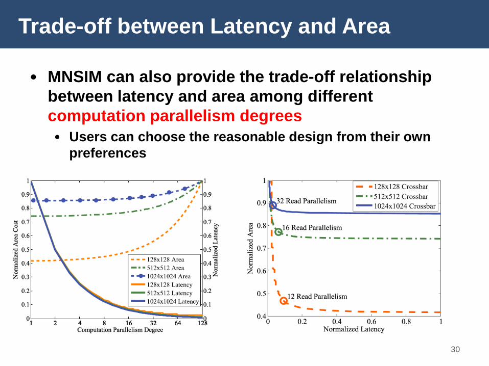
Trade-off between Latency and Area
• MNSIM can also provide the trade-off relationship
between latency and area among different
computation parallelism degrees
• Users can choose the reasonable design from their own
preferences
30

Outline
• Background
• Circuit Structure and Module Design
• Simulation Models
• Experimental Results
• Future Work
31
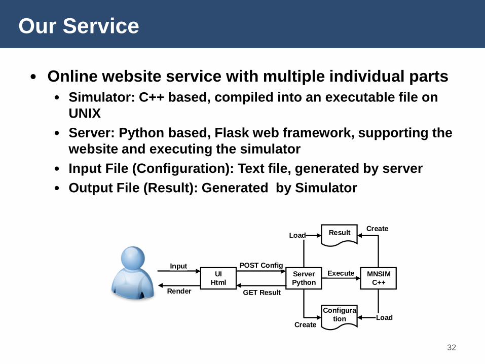
Our Service
• Online website service with multiple individual parts
• Simulator: C++ based, compiled into an executable file on
UNIX
• Server: Python based, Flask web framework, supporting the
website and executing the simulator
• Input File (Configuration): Text file, generated by server
• Output File (Result): Generated by Simulator
32
UI
Html
Server
Python
Configura
tion
MNSIM
C++
Result
POST ConfigExecute
CreateLoad
CreateLoad
GET Result
Input
Render

References
[1] Liu, Daofu, et al. "Pudiannao: A polyvalent machine learning accelerator." Proceedings of the Twentieth International Conference on Architectural Support for Programming Languages and Operating Systems. ACM, 2015.
[2] http://www.intel.com/content/www/us/en/architecture-and-technology/3d-xpoint-unveiled-video.html
[3] http://www.sagestorage.eu/
[4] Miao Hu, Hai Li, et al. “Hardware realization of BSB recall function using memristorcrossbar arrays” DAC'2012, San Francisco, USA, June.03-07, 2012
[5] P. A. Merolla, et al. “A million spiking-neuron integrated circuit with a scalable communication network and interface,” Science, vol. 345, no. 6197, pp. 668–673, 2014.
[6] Dong Xiangyu, et al. "Nvsim: A circuit-level performance, energy, and area model for emerging nonvolatile memory." Computer-Aided Design of Integrated Circuits and Systems, IEEE Transactions on 31.7 (2012): 994-1007.
[7] Matthew Poremba, and Xie Yuan. "Nvmain: An architectural-level main memory simulator for emerging non-volatile memories." VLSI (ISVLSI), 2012 IEEE Computer Society Annual Symposium on. IEEE, 2012.
[8] Li Boxun, et al. "Merging the Interface: Power, Area and Accuracy Co-optimization for RRAM Crossbar-based Mixed-Signal Computing System." DAC, 2015.
33

Thank you!
Q&A

• For multi-layer network, the errors are accumulated
through layers
• Given the quantization interval Vinterval, the quantization boundaries
are (0.5Vinterval, 1.5Vinterval,..., (k – 1-0.5) Vinterval)
• In the worst case, the ideal computing result signal is just around
the largest quantization boundary (k – 1.5) Vinterval and needs to be
recognized as the maximum value k - 1
• For average situation, the digital deviation of a specific quantization
level i can be represented by 𝒊𝜺 + 𝟎. 𝟓 , so:
• Finally, we can estimate the error rate of next layer by:
Propagating of Error Rate
35
MaxErrorRate=𝑘−1.5 𝜀+0.5
𝑘−1
AvgErrorRate= 𝑖=0𝑘−1 𝑖𝜀+0.5
𝑘(𝑘−1)
(1 + 𝛿1)(1 + 휀2)𝑉𝑖𝑑𝑒𝑎𝑙 ≤ 𝑉𝑎𝑐𝑡𝑢𝑎𝑙 ≤ (1 + 𝛿1)(1 + 휀2)𝑉𝑖𝑑𝑒𝑎𝑙