mnoc : a network on chip for monitors
TRANSCRIPT

University of Massachusetts Amherst University of Massachusetts Amherst
ScholarWorks@UMass Amherst ScholarWorks@UMass Amherst
Masters Theses 1911 - February 2014
January 2008
MNoC : A Network on Chip for Monitors MNoC : A Network on Chip for Monitors
Sailaja Madduri University of Massachusetts Amherst
Follow this and additional works at: https://scholarworks.umass.edu/theses
Madduri, Sailaja, "MNoC : A Network on Chip for Monitors" (2008). Masters Theses 1911 - February 2014. 215. Retrieved from https://scholarworks.umass.edu/theses/215
This thesis is brought to you for free and open access by ScholarWorks@UMass Amherst. It has been accepted for inclusion in Masters Theses 1911 - February 2014 by an authorized administrator of ScholarWorks@UMass Amherst. For more information, please contact [email protected].

MNoC: A NETWORK ON CHIP FOR MONITORS
A Thesis Presented
by
SAILAJA MADDURI
Submitted to the Graduate School of the
University of Massachusetts Amherst in partial fulfillment
of the requirements for the degree of
MASTER OF SCIENCE IN ELECTRICAL AND COMPUTER ENGINEERING
September 2008
Electrical and Computer Engineering

© Copyright by Sailaja Madduri 2008
All Rights Reserved

MNoC: A NETWORK ON CHIP FOR MONITORS
A Thesis Presented
by
SAILAJA MADDURI
Approved as to style and content by:
____________________________________
Russell G. Tessier, Chair
____________________________________
Wayne P. Burleson, Member
____________________________________
Sandip Kundu, Member
__________________________________________
C.V. Hollot, Department Head
Electrical & Computer Engineering

iv
ACKNOWLEDGMENTS
I would firstly like to thank my parents and my sister for being so immensely supportive
all through the years. Many many thanks to my advisor Prof Tessier for spending so
much time on giving my thesis a shape , taking the time out to meet with me every single
day and guiding me to completion. It was a pleasure to come into the lab to work. I am
also grateful to Prof Burleson and Prof Kundu for serving on my committee and
providing me with valuable feedback time and again.
Special thanks to Ramakrishna for all the insightful discussions, for reading over all my
documents and for helping me stay motivated. Thanks to all my friends back home and to
everyone at Amherst who made my stay here a smooth and pleasant one.
.

v
ABSTRACT
MNoC: A NETWORK ON CHIP FOR MONITORS
SEPTEMBER 2008
SAILAJA MADDURI
B.E (Hons) ., BIRLA INSTITUTE OF TECHNOLOGY AND SCIENCE, INDIA
M.S.E.C.E, UNIVERSITY OF MASSACHUSETTS AMHERST
Directed by: Professor Russell G. Tessier
As silicon processes scale, system-on-chips (SoCs) will require numerous hardware
monitors that perform assessment of physical characteristics that change during the
operation of a device. To address the need for high-speed and coordinated transport of
monitor data in a SoC, we develop a new interconnection network for monitors - the
monitor network on chip (MNoC). Data collected from the monitors via MNoC is
collated by a monitor executive processor (MEP) that controls the operation of the SoC in
response to monitor data. In this thesis, we developed the architecture of MNoC and the
infrastructure to evaluate its performance and overhead for various network parameters.
A system level architectural simulation can then be performed to ensure that the latency
and bandwidth provided by MNoC are sufficient to allow the MEP to react in a timely
fashion. This typically translates to a system level benefit that can be assessed using
architectural simulation. We demonstrate in this thesis, the employment of MNoC for
two specific monitoring systems that involve thermal and delay monitors. Results show
that MNoC facilitates employment of a thermal-aware dynamic frequency scaling scheme
in a multicore processor resulting in improved performance. It also facilitates power and
performance savings in a delay -monitored multicore system by enabling a better than
worst case voltage and frequency settings for the processor.

vi
TABLE OF CONTENTS
ACKNOWLEDGMENTS ................................................................................................. iv
ABSTRACT........................................................................................................................ v
1. INTRODUCTION .......................................................................................................... 1
2. BACKGROUND AND PREVIOUS WORK................................................................. 8
2.1 Existing On-Chip Monitoring Approaches............................................................... 8
2.1.1 Thermal Monitors .............................................................................................. 8
2.1.2 Soft Error Monitors.......................................................................................... 10
2.1.3 Critical Path Delay Monitor............................................................................. 11
2.1.4 Collaborative Monitoring................................................................................. 13
2.1.5 Monitoring Wrap-up ........................................................................................ 14
2.2 Previous Work on Monitoring Based Control ........................................................ 15
2.2.1 Temperature and Power Measurements to Optimize Performance ................. 15
2.2.2 SoC Resource Manager Based on Temperature and Performance Feedback…
................................................................................................................................... 16
2.2.3 Hardware and Software Monitoring to Reconfigure Processor Resources...... 17
2.2.4 Circuit level Timing Error Detection for Low Power Operation..................... 17
2.2.5 Summary of Monitoring Based Control Techniques ....................................... 18
2.3 Existing Approaches to On-Chip Communication ................................................. 20
2.3.1 Bus Based Interconnections ............................................................................. 21
2.3.2 Point to Point Connections............................................................................... 22
2.3.3 Networks on Chip (NoC) ................................................................................. 23
2.2.3.1 Statically Scheduled Network................................................................... 24
2.2.3.2 Dynamic Network..................................................................................... 24
3. MNoC ARCHITECTURE............................................................................................ 30
3.1 MNoC Components and Features........................................................................... 30
3.2 MNoC Topology and Connections ......................................................................... 31
3.3 MNoC Packets ........................................................................................................ 32
3.4 MNoC Routing Protocol......................................................................................... 34
3.5 The MNoC Router .................................................................................................. 35
3.6 MNoC Router – Monitor Interface ......................................................................... 39
3.7 Monitor Executive Processor – Network Interface................................................. 40

vii
4. MNoC VALIDATION APPROACH ........................................................................... 42
4.1 MNoC Performance Evaluation.............................................................................. 42
4.2 MNoC Overhead Estimation .................................................................................. 44
4.3 MNoC System Level Validation............................................................................. 45
5. EXPERIMENTAL APPROACH AND RESULTS FOR VALIDATING MNOC...... 47
5.1 Thermal Management Using MNoC ...................................................................... 47
5.1.1 Interconnect simulation results ........................................................................ 49
5.1.2 Hardware estimation results............................................................................. 51
5.1.3 Architectural simulation results ....................................................................... 52
5.2 Voltage Droop Management Using MNoC ............................................................ 54
5.2.1 Modifying voltage in response to voltage droop ............................................. 56
5.2.2 Modifying frequency in response to voltage droop ......................................... 63
6. CONCLUSIONS AND FUTURE WORK ................................................................... 67
BIBLIOGRAPHY............................................................................................................. 68

viii
LIST OF TABLES
Table 1: Summary of monitoring based control techniques ............................................. 20
Table 2 : MNoC area results ............................................................................................. 52
Table 3 : Runtimes for MNoC and non-MNoC cases....................................................... 54
Table 4 :Variation of initial supply voltage for the MNoC based system as the monitor
sampling rates vary ........................................................................................................... 59
Table 5: MNoC area estimates for the 9 router configuration .......................................... 63
Table 6 : Variation of initial frequency for the MNoC based system as the monitor
sampling rates vary ........................................................................................................... 64

ix
LIST OF FIGURES
Figure 1: Clock Skew Variation for a Dual Core ................................................ ……….. 1
Figure 2: IBM POWER4 chip temperature against its functional units [46]...................... 1
Figure 3: Conceptual diagram of MNoC on a quad core processor ................................... 3
Figure 4 : Thermal Sensors on a bus [28]………………………………………………... 4
Figure 5 : Foxton Power Control loop [6] .......................................................................... 4
Figure 6: Ring Oscillator based thermal sensor [33]……………………………………...9
Figure 7: Ring Oscillator Temp Vs Freq[5]........................................................................ 9
Figure 8: Thermal System block diagram[6] ...................................................................... 9
Figure 9: Critical Path Monitor, IBM Power 6 processor [20] ......................................... 12
Figure 10: Collaborative monitoring with thermal and processing monitors [18] ........... 14
Figure 11: High level overview of the Foxton control system [37].................................. 15
Figure 12: Pipeline stage augmented with Razor latches and control lines [32] .............. 18
Figure 13: SoC resource manager controlling frequency based on thermal information
from sensors [27] ...................................................................................................... 23
Figure 14: Generic NoC architecture [24] ........................................................................ 25
Figure 15: Detailed view of MNoC for multiple cores..................................................... 31
Figure 16 : MNoC packet format...................................................................................... 33
Figure 17 : Sample MNoC routing table........................................................................... 34
Figure 18: MNoC router architecture ............................................................................... 36
Figure 19 : MNoC monitor – network router interface..................................................... 39
Figure 20 : MEP -Network interface ................................................................................ 41
Figure 21 : MNoC validation approach ............................................................................ 45

x
Figure 22 : Monitor network on chip layout for thermal monitors on a 8 core
processor……………………………………………………………………………48
Figure 23 : Regular channel latencies for different buffer sizes ....................................... 50
Figure 24 : Priority channel latencies for different buffer sizes ....................................... 50
Figure 25 : Regular channel latencies for different flit widths ........................................ 51
Figure 26 : Single droop recovery using MNoC............................................................... 56
Figure 27 : Power savings with MNoC on a 4 core processor.......................................... 60
Figure 28: Power savings with MNoC on a 8 core processor........................................... 60
Figure 29 : Power savings with MNoC on a 16 core processor ....................................... 60
Figure 30: Power savings with increasing MNoC bandwidth on a 16 core processor ..... 61
Figure 31: Variation in power savings with variable MNoC buffer sizes ........................ 62
Figure 32 : Quantifying MNoC area overhead ................................................................. 63
Figure 33: Performance benefit in multi-cores using MNoC ........................................... 65
Figure 34: Performance benefit with varying MNoC bandwidth ..................................... 66

1
CHAPTER 1
INTRODUCTION
Systems on Chips (SoCs) are becoming increasingly complex as large numbers of cores
are integrated into single-chip platforms. These systems typically exhibit stringent
processing, communication, and power constraints that must be carefully addressed
during system design. As the size and diverse use of SoCs increase, the importance of
run-time monitoring of correct functionality and system performance increases. Real-time
system monitoring is crucial to determine if a system is operating as designed and is
executing within designed parameters. Figure 1 provides an example of the effect of
environmental factors on a computing device. The clock skew distribution for an Intel
Xeon Processor [14] clearly shows a wide skew variation across the die. Figure 2 [46]
illustrates the full-chip temperature variation profile. Such increasing variations in device
operating conditions motivate the need for a more “operating conditions aware” design.
Figure 1: Clock Skew Variation for a Dual Core Figure 2: IBM POWER4 chip temperature
profile against its functional units [46]
Recent high-end processors from Intel (Montecito), AMD (Opteron) and IBM (Cell) use
extensive on-chip monitors for run-time estimates of temperature, power, clock jitter,

2
supply noise and performance behavior. The main benefits of these monitoring modules
are:
• They quickly evaluate system performance without interfering with the primary
operation of the SoC.
• They facilitate a better-than-worst-case design that enables better power and
performance
In order to maximize monitor effectiveness, monitor data often needs to be collated from
across the chip and evaluated in real time as a SoC operates. This data can then be used to
alter SoC operation in response to environmental conditions. Although on-chips monitors
are becoming increasingly common in current day SoCs and processors, a unified
approach to their interconnection, verification, test and debug has not been developed yet.
The main contribution of this work is the development and validation of a scalable,
flexible and light weight interconnection network for monitor interaction, the Monitor
Network on Chip (MNoC). The Monitor Network on Chip interfaces with various kinds
of monitors distributed across the chip, collects monitor data and routes it to the Monitor
Executive Processor (MEP). The MEP evaluates this data and interfaces back into the
system to take necessary actions which ensure correct operation, performance savings,
power savings or various other benefits. As seen in Figure 3 , the MNoC platform
involves the integration of numerous on-chip monitors to form a complete chip
subsystem devoted to monitoring.

3
`
Proc 0 Proc 1
Proc 3Proc 2
L2 Cache
L2 Cache
Voltage droop monitorCache-bank error monitorThermal sensorDelay monitorMEP – Monitor executive processor
MEPMEPMEPMEP
MNoC
Figure 3: Conceptual diagram of MNoC on a quad core processor
Recently, a number of research projects have examined the use of monitors in controlling
the behavior of SoCs. The Montecito processor [6] uses voltage and temperature sensors
to control processor power consumption. Temperature and voltage values are sampled
with A/D converters and transferred to a controller which modulates system clock
frequency and voltage. The Razor architecture [32] utilizes shadow latches to determine
if signal delay violations have occurred due to voltage reductions. Monitors evaluate the
number of errors that have occurred and update core voltage. Cache miss rates and
branch prediction monitors have been used in [31] to reconfigure processor resources in
real time. This information can include event counts and frequencies. System resources
are reconfigured by a centralized control circuit. The SoC resource manager described in
[27] allows for dynamic bandwidth allocation for the IP cores based on the required
bandwidth. This is done by monitoring the difference in between actual operation speed
and the target operation speed. The higher the difference, higher is the priority for

4
bandwidth allocation. The IBM Power6 architecture [48] interconnects multiple sensors
and actuators via a high-speed serial bus. Addressable registers are used as the interfaces
to these components. The described interconnect primarily serves as an external interface
to voltage and thermal control via an I2C bus.
Most monitoring based control explored so far is restricted to a few localized monitors
which did not demand a highly scalable communication medium. Hence most of the
current monitor interconnection approaches are either direct point to point connections or
buses. For example, Figure 4 [28] shows an FPGA based thermal monitoring system
which involves a controller and an array of temperature sensors. The sensors are
connected to the Power PC processor on the Xilinx Virtex-2 Pro FPGA using the On-
Chip Peripheral bus (OPB). Figure 5 shows the embedded feedback control system of
Intel’s Montecito processor [6] which dynamically maximizes performance per Watt by
using readings from 4 on-chip thermal sensors and voltage sensors. As seen in the figure,
the sensors are directly connected to the micro-controller via analog-to-digital converters
using point-to-point connections.
Figure 4 : Thermal Sensors on a bus [28] Figure 5 : Foxton Power Control loop [6]
POWER PC
PROCESSOR
ON CHIP PERIPHERAL
BUS
TS
TS
TS
TS
TsS – THERMAL
SENSOR

5
Intel’s Montecito processor uses four thermal sensors per chip, the more recent IBM
Power6 processor employs 24 thermal sensors per chip and these monitor numbers are
only expected to increase. As silicon processes scale, it is expected that future SoCs will
generally include numerous embedded monitors to take advantage of the power and
performance benefits that monitors can offer. We believe that the poor scalability of
buses [23] and the exponential increase in the number of required point-to-point
connections [24] will limit their usage for monitor interconnections in the future and that
a more scalable and segmented monitor interconnect will become essential.
Recently, Networks on chip (NoC) [23][28][29] have gained importance as
communication structures that provide enhanced performance in comparison with
previous communication architectures. NoCs are perceived as the scalable, global
alternatives to traditional buses. They however entail a high area overhead [24] and are
not, in entirety, appropriate for monitor interconnections. Due to the various limitations
discussed above, no existing interconnection approach is fully suitable to serve as a
monitor interconnection network.
We view the integration of monitors and the collection and processing of monitor
information as an important unaddressed SoC design issue. As an initial step in the
development of a complete monitor subsystem for SoCs, a low-overhead on-chip
interconnect, which is optimized for monitors, has been designed as a part of this thesis
project. MNoC was built on existing approaches like Networks on Chip, buses,
multiplexers and point to point connections with emphasis on scalability and low
resource overhead. Although simplified compared to other on-chip interconnect

6
approaches, our new interconnect technique supports irregular routing topologies, priority
based data transfer and customized monitor interfacing. Collected monitor data values are
manipulated by a monitor executive processor and the results are used to control SoC
run-time operation.
The efficiency of our monitor interconnect is assessed for a multicore system employing
two different monitoring systems, a thermal and a delay monitoring system. A monitoring
system typically consists of a set of monitors, MNoC for data transfer, the Monitor
Executive Processor that evaluates monitor data, the actuator that performs actions in
response to monitor data and the corresponding network interfaces. Experimental results
were generated using both interconnect and a system-level simulators and results show
that the new low-overhead monitor interconnect facilitates employment of a thermal-
aware dynamic frequency scaling scheme in a multi-core processor. The new MNoC also
enables an approach that allows the countering of voltage drop problems dynamically
during run time without relying entirely on packaging techniques. The overhead and
performance of the monitor network-on-chip interconnect for an eight core
multiprocessor has been measured via hardware synthesis, interconnect simulation, and
multicore architectural simulation. For an eight core thermal monitoring system, the area
overhead of MNoC is found to be less than 1%. MNoC also enables around 15%
power/performance benefit in both the test systems.
The rest of the thesis is organized as follows. Chapter 2 discusses the previous work that
has been done in the area of monitors and monitoring based control. This chapter also
includes a discussion on existing on-chip interconnection approaches, focusing on

7
Networks on Chip. Chapter 3 gives a description of the MNoC architecture, the various
MNoC components, the network interfaces, and protocols. Chapter 4 gives the approach
to MNoC validation and describes the simulation setup for the new interconnect. Chapter
5 describes the experimental approach for the two sample systems and presents the
results. The summary of the thesis work and some direction for future work are provided
in Chapter 6.

8
CHAPTER 2
BACKGROUND AND PREVIOUS WORK
2.1 Existing On-Chip Monitoring Approaches
Increased SoC integration is increasing chip reliability and power concerns, making
monitors for temperature, power, clock jitter, supply noise and performance behavior an
integral part of current day SoCs. This section gives a detailed description of some
contemporary SoC monitors and their implementations. The thermal, delay and error
monitors which are parts of our prototype systems are emphasized in this section.
2.1.1 Thermal Monitors
As the sophistication of embedded systems and the power density of silicon devices
increase, temperature-related system effects become more important. For example, disk
drives in embedded systems are severely susceptible to erroneous operation at high
temperatures. If ambient temperature increases by 5 degrees Celsius over the design
specification, disk drives are 15% more likely to fail[4].Temperature can reduce
performance by lowering output-voltage swings, reducing switching speeds, lowering
noise margins, and reducing signal quality. In addition to performance loss, temperature
stresses also reduce system reliability [4].
Many temperature sensors are based on ring oscillators, similar to the type shown in
Figure 6. A ring oscillator’s delay dependence on temperature provides an effective way
to measure the temperature of a chip. In general, the oscillation frequency of the sensor
exhibits a linear dependence on junction temperature. Each rising edge of fout stimulates a
count cycle in a counter. The count achieved over a period of time indicates the

9
temperature inside the device. An increase in temperature extends the period of the ring
oscillator, leading to smaller count values in the same time period. This effect is
illustrated in Figure 7.
Figure 6: Ring Oscillator based thermal sensor [33] Figure 7: Ring Oscillator Temp Vs Freq[5]
A thermal sensor implementation that exploits the temperature co-efficient of a forward
biased diode voltage (Vbe) is shown in Figure 8 . The thermal sensor consists of a pFET
current source, which drives a diode with a constant current.
Figure 8: Thermal System block diagram[6]
The sensor has been used as part of a thermal management system in [6]. Since voltage
Vbe fluctuates with temperature, voltage variations are created at the inputs to the A/D
converters. The measured voltage is converted into a temperature value by comparing the

10
input voltage with a calibrated Vbe value and the characterized temperature coefficient.
The result of this comparison is provided to a microcontroller, which can take appropriate
action. In this case, system clock frequency can be decreased to reduce temperature, if
necessary.
2.1.2 Soft Error Monitors
As system operating frequencies increase and power supply voltages are reduced,
transient faults become a major source of problems as they increase device soft error
rates. Often, memory buses are extended to accommodate extra bits that detect and
correct errors. CRC (cyclic redundancy checking) codes are used to detect and sometimes
correct accidental alteration of data during transmission in communication systems.
Specifying a CRC involves modifying a bit stream based on a CRC polynomial.
Corrections can be performed via the retransmission of data [36] if the CRC codes do not
have an inherent error correcting capability.
The detection of soft errors in a processor core’s logic presents a more difficult challenge
than the detection on errors in memory [15] . Backward recovery through checkpointing
and rollback is a popular approach used in modern processors to recover from these kinds
of transient faults.
A soft error detection scheme for processor core logic described in [15] uses a dual
modular redundancy technique. In this technique, two redundant processors execute
simultaneously and an error in execution in one processor manifests as a deviation in the
behavior of the two processors. The deviation in behavior is evaluated based on a
“fingerprint” comparison of the states of the two processors at regular checkpoint

11
intervals. A checkpoint of a program state consists of a snapshot of the registers and
memory at a specific point of time. A checkpoint interval is the time between two
successive checkpoints. A fingerprint is a hash value that summarizes the states of the
processors after every instruction in the checkpoint interval. If the fingerprints for both
processors agree at the end of the checkpoint interval, all instructions executed during the
interval are known to be correct. If the fingerprints disagree, the processor must be rolled
back to the last correct state of execution, which is the checkpoint at the beginning of the
current interval. This scheme avoids the need to compare all architectural state updates,
but still captures a summary of all state changes in the fingerprint value.
2.1.3 Critical Path Delay Monitor
Process variation, supply noise effects, aging effects, clock instability and reliability
based failure mechanisms can be characterized by a change in delay of the critical path of
the circuit. A critical path monitor is used for identifying the effects of these variations on
the critical path and for taking necessary action. This corrective action could be
increasing voltage or decreasing the frequency so as to prevent the circuit from failing.
The IBM Power6 processor employs [20] 24 critical path monitors (CPMs) distributed
across the chip which guarantee correct circuit operation under different process, voltage
and temperature conditions. The critical path monitor, shown in Figure 9, consists of 5
delay paths – 4 NAND gates, Series 3 NOR Gates, Adder Path, Wire dominated path,
Series pass-gates, each with different delay sensitivities to process, voltage or
temperature.

12
Figure 9: Critical Path Monitor, IBM Power 6 processor [20]
The critical path monitor also contains two edge path detectors which consist of a 12-
inverter delay line with capture latches at each inverter output. On each rising edge of the
system clock, an edge is launched into these paths and the same edge is also given to
edge detectors which use it as a reference (A in the figure). The edge B which passes
through the chosen path is latched in the edge detector at the rising edge of the system
clock and is compared with the reference value A.
The output of the critical path monitor is thus a digital code indicating how far the edge
propagated through the edge detector. This is an indicator of the delay on the selected
path. The paths however do not exactly track the critical path of the circuit and should be
calibrated initially for accuracy. The digital code needs to be sampled every clock cycle
and hence this monitor has a large bandwidth, requiring a network like interconnection
approach for data collection.

13
2.1.4 Collaborative Monitoring
In many cases it may be desirable to use information from multiple monitors to validate
information against each other. A monitoring system that allows collaboration between a
processing and thermal monitor is described in [18] . The thermal monitor used in [18] is
the ring oscillator based thermal monitor described in Section 2.1.1. The processing
monitor evaluates whether the processor is operating within expected parameters by
comparing the results of an off-line analysis of the system binary to run-time information
obtained from the processor core.
A monitoring graph that represents the sequence of control flow, instruction addresses,
and opcodes is generated off-line by simulating the binary of the application. During run-
time, the embedded processor reports on the progress of the application, by sending a
stream of information to the monitoring system. The monitoring system then compares
the stream to the expected behavior of the program from the monitoring graph. Run-time
uncertainties and embedded system faults that cause deviations from intended behavior
can then be detected by the monitor. The size of the monitoring graph determines the
overhead of the monitor.
The block diagram of this monitoring system is shown in Figure 10. Temperature
information from the thermal monitor can be correlated with monitoring graphs in the
processing monitor to allow for more robust evaluation. The monitoring graphs identify
power-intensive program regions that dissipate substantial heat and it can be expected
that these regions will report high temperatures. If thermal information is used without
considering the processing context, the static thermal alarm threshold could either be too

14
conservative (i.e., causing false alarms in regions of intense processing) or too optimistic
(i.e., opening avenues for run-time problems that cannot be detected) [18]. Collaborative
monitoring addresses these kinds of scenarios. MNoC allows for easy collaborative
monitoring by integrating different kinds of monitors to one monitoring sub system.
Figure 10: Collaborative monitoring with thermal and processing monitors [18]
2.1.5 Monitoring Wrap-up
The proposed Monitor Network on Chip is an effort to allow different kinds of monitors
to communicate with a central controller that evaluates monitor data and takes necessary
action in the case of unexpected system behavior. Typical responses could be frequency
throttling, voltage reduction or resource reconfiguration depending on the exact nature of
the deviation from expected system operation. This section described a series of
candidate monitors and their operation.

15
2.2 Previous Work on Monitoring Based Control
This section discusses existing implementations of monitoring based control, where data
from the previously discussed monitors is used to impact system behavior.
2.2.1 Temperature and Power Measurements to Optimize Performance
An embedded feedback control system in [6] dynamically maximizes performance per
watt in a 90-nm Itanium family processor based on information from voltage, thermal and
power sensors. The control system, referred to as Foxton Technology (shown in Figure
11), utilizes on-chip sensors to measure power and temperature and modulates both
voltage and frequency using an embedded microcontroller to optimize performance while
meeting power and temperature constraints. As a result, the processor cores perform
computation at optimal power efficiency.
Figure 11: High level overview of the Foxton control system [37]
Core power that is measured at regular intervals during processor operation is calculated
from the core voltage that is sampled with on-die A/D converters. On-die diode-based
temperature sensors (Figure 8) enable temperature control. Thermal information is used

16
in conjunction with the power measurements to vary the core voltage. These new voltage
values are communicated to the Montecito voltage regulator by the embedded controller.
The clock system responds to voltage changes and the clock frequency is tuned such that
the system is at an optimal power, temperature, voltage, frequency envelope. This
operating point maximizes performance per Watt at a specific point of time. The entire
measurement and control system is embedded within the die. The area overhead for this
system is about 0.5% of the die area and the power overhead is approximately 0.5% of
die power. This system can be visualized as a small MNOC, with temperature and
voltage monitors connected to a micro-controller that manages the system.
2.2.2 SoC Resource Manager Based on Temperature and Performance Feedback
As the number of intellectual property blocks in SoCs increases, effective distribution of
resources like power and data bandwidth becomes increasingly important. A SoC
resource manager which is responsible for supervising the allocation of resources to IPs
using information monitored from the SoC is described in [27] . The monitors include
thermal monitors for temperature information, and performance monitors for information
about the operating frequency of various IPs on the chip. The information from the
thermal monitors is used by the resource manager to reduce the chip operating frequency
taking into account the environmental temperature. The performance monitor gives
information about the operation speed of the IPs to the controller. This information is
used by the resource manager to calculate the priority of data-access requests by each IP
based on the difference between the actual operation speed and the target operation
speed. The larger the difference between the actual speed and the target speed, the higher
the priority. This approach allows dynamic IP bandwidth allocation.

17
2.2.3 Hardware and Software Monitoring to Reconfigure Processor Resources
Processor resource reconfiguration can be used to reduce power consumption with the
assistance of hardware monitoring and software profiling [31] .Hardware monitors
measure recent processor performance by establishing a pattern for a certain interval of
execution. Hardware monitoring can collect statistics such as instructions per cycle (IPC),
resource utilization, and instruction dependencies. Software profiling is performed by
collecting similar statistics, such as IPC and L2 cache miss rates. Software profiling can
identify behavior over a short program run and then annotate instructions to identify this
behavior for future code execution. A collaborative approach in [31] combines both
hardware and software profiling to reconfigure processor resources. This approach has
better power-performance trade-offs than individual hardware or software profiling based
resource reconfiguration.
Two power saving configuration techniques are considered for the processor. The
instruction issue width can be reduced as the IPC drops. Power savings are obtained by
disabling one of the functional units and reducing the issue width. The second kind of
power savings mechanism considered is fetch halting. In this case, fetching is limited
while the processor is stalled for an extended period of time due to a long latency cache
miss. This approach saves power by reducing occupancy rates in the fetch and issue
queues thereby allowing portions of these structures to be more effectively disabled.
2.2.4 Circuit level Timing Error Detection for Low Power Operation
To ensure correct operation of a processor under all possible variations, typically a
conservative supply voltage that uses worst case parameters is chosen. This choice

18
supports a worst case combination of variations which is highly unlikely and makes the
approach overly conservative. Razor, a dynamic voltage scaling approach which uses
dynamic detection and correction of circuit timing errors to tune the processor supply
voltage is described in [32]. With a dynamic voltage scaling approach like this, an overly
conservative supply voltage can be avoided and consequently power can be saved. In
[32], the supply voltage is tuned based on the error rate in the circuit. A shadow latch
controlled by a delayed clock, as shown in Figure 12, is used to detect timing errors in the
circuit. A very low error rate indicates that the computation is finishing with slack, so the
supply voltage could be lower. Increased error rates indicate that the voltage supply
should be increased.
Figure 12: Pipeline stage augmented with Razor latches and control lines [32]
2.2.5 Summary of Monitoring Based Control Techniques
Table 1 summarizes the previous work regarding control of system operation based on
monitor data. In general, monitor/system interactions can yield good power savings
without sacrificing significant system performance. The examples described in this

19
section re-emphasize the importance of on-chip monitoring and the need for low
overhead interconnect between monitors and a control resource (e.g. the MEP). System-
level modifications can be made by the MEP after monitor data is evaluated. To address
the need for high-speed and coordinated transport of monitor data in a system-on-chip,
we require an interconnection structure that helps assemble monitor data with the lowest
possible overhead. The next section is a summary of existing on-chip interconnection
approaches which can possibly serve as monitor interconnects
S.NO REFERENCE MONITORS
INVOLVED
RESPONSE TO
MONITOR DATA
1 Feedback control
system in Intel
Montecito Processor[6]
Voltage monitor,
Thermal monitor
A microcontroller modulates
frequency and voltage while
meeting temperature and
power constraints
2 SoC resource manager
to control performance
and data bandwidth
allocation [27]
Thermal monitor,
Performance monitor
The SoC resource manager
controls performance based
on temperature and also
handles data bandwidth
allocation to the IPs
3 Processor resource
reconfiguration [31]
Hardware processor
performance monitors
and software profiling
get information about
branch prediction,
cache misses etc
Processor resource
reconfiguration using
information from hardware
monitors and software
profiling
4 Razor shadow latches
for circuit level timing
error detection [32]
Shadow latches along
critical paths to detect
and correct timing
errors
The error rate is used to tune
the processor voltage. With
a low error rate, voltage can
be reduced

20
5 Bulletproof mechanism
to protect
microprocessor pipeline
and memory system
from silicon defects
[19]
Distributed BIST
mechanisms to validate
the integrity of
underlying hardware
during specific epochs
In case of an error, program
state is rolled back and the
disabled component is
removed to let the processor
run in a sub-optimal
performance mode
Table 1: Summary of monitoring based control techniques
2.3 Existing Approaches to On-Chip Communication
Since the introduction of the SoC concept, the solutions for SoC communication
structures have generally been characterized by custom designed ad hoc mixes of buses
and point-to-point links. More recently, networks on chip (NoC) [23][38][39] have
gained importance as valuable alternatives to buses. This section describes various on-
chip interconnection techniques that are currently used in SoCs and examines the
pertinence of these techniques for MNoC. Specifically, the following characteristics of
monitor interactions need to be addressed by a medium that serves as a monitor network
on chip (MNoC).
1) The bandwidth requirements for MNoC monitors are very diverse and are generally
lower than the bandwidth requirements of typical SoC cores, such as microprocessors
and associated memory.
2) The monitors are laid out on the chip in a very irregular fashion and hence the
network could be irregular unlike typical SoC networks.
3) A generalized monitor interface is difficult to specify because of the diversity of
monitors.
4) The number and kind of on-chip monitors included per SoC are likely to increase in
the coming years. As a result, a MNoC needs to be scalable to support increased
monitor diversity and count.

21
5) Architectural support for monitors and associated interconnect must be lightweight
and consume minimal system resources.
2.3.1 Bus Based Interconnections
Buses constitute the straightforward form of SoC communication that is widely used in
contemporary SoCs. In a bus based interconnection, several communicating modules are
connected to a set of shared wires and an arbiter controls data transfer on the bus. The
arbiter evaluates requests from various peripherals and grants one of the requesters access
to the bus, based on the arbitration mechanism that it employs. Buses are simple and easy
to build. However, they suffer from a variety of disadvantages like poor scalability .Their
limitations are causing a shift towards alternative, more scalable communication models.
An FPGA thermal monitoring system described in [5] involves the connection of
temperature sensors and a controller using the On-Chip Peripheral bus (OPB) in the
Xilinx Virtex-2 Pro FPGA. Sensor information that is read by the controller through the
OPB bus can be used to implement various dynamic thermal management schemes.
The number of monitors that can be connected to a bus is limited by its scalability. If
numerous SoC monitors need to communicate to a centralized destination like in MNOC,
a bus, by itself, is likely unsuitable. As the need for monitor integration increases, more
monitors need to be integrated using the bus and the performance of the bus begins to
degrade. Bus arbitration delays increase with the number of peripherals. Also, bandwidth
is shared among multiple monitors and the shared bandwidth might not suffice for some
higher data rate monitors like the critical path delay monitors explained in Section 2.1.3 .
The IBM Power6 architecture [48] interconnects multiple thermal, delay sensors and

22
actuators via a high-speed serial bus. Addressable registers are used as the interfaces to
these components. Scalability is still an issue with such a type of interconnect. For
maximum flexibility and scalability, a move towards a shared, segmented communication
structure is required.
One other alternative available is to use the existing debug data channels for transporting
MNoC data. The JTAG boundary scan interface [49] provides a serial scan interconnect
which typically operates at 1 MHz. This low bandwidth chain consumes a minimal
amount of resources and provides scalability. A recent, enhanced debug system [50] uses
multiplexers to collate debug information to one or more debug control points. Unlike
MNoC, debug subsystems do not attempt to use collected information to influence SoC
run-time operation.
2.3.2 Point to Point Connections
Point–to-point links between a set of communicating modules allow for dedicated inter-
module communication. The full link bandwidth is always available and hence dedicated
point-to-point links provide the best possible bandwidth and latency. However, they
require a significant hardware overhead and the number of links increases exponentially
with the number of cores [24].
Point-to-point connections have been traditionally used for monitor data transport
because the limited number of monitor connections did not cause a significant overhead.
The thermal sensors on Intel’s Montecito processor [6], described in Section 2.2.1, are
directly connected to the micro-controller via analog-to-digital converters using point-to-
point connections. The resource manager in [27] controls system operating frequency and

23
IP bandwidth allocation using readings from thermal and performance monitors, as
described in Section 2.2.2. The connection between the resource manager and the
monitors is a point-to-point connection as evident from Figure 13.
Figure 13: SoC resource manager controlling frequency based on thermal information from sensors
[27]
Point-to-point connections can be a good choice of interconnection for a small number of
closely located monitors. Since we anticipate that MNoC will cater to a number of
different kinds of monitors, it will not be realistic to assume a point-to-point connection
from every monitor to the MEP. Such point-to-point connections for MNoC would result
in a significant resource overhead.
2.3.3 Networks on Chip (NoC)
NoC is an approach for communications within large VLSI systems implemented on a
single silicon chip. In a NoC system, modules such as processor cores, memories and
specialized IP blocks exchange data using a network. A NoC is constructed from multiple
point-to-point data links interconnected by switches (or routers), such that messages can
be relayed from any source module to any destination module over several links, by
making routing decisions at the switches. Two important metrics that evaluate the quality

24
of a network-on-chip are bandwidth1
and latency. Bandwidth indicates the amount of data
that can be put on the network in a given amount of time and latency indicates delay
experienced by data in traveling from the source to the destination, along the network.
Generally, two kinds of NoC implementations are used in contemporary systems:
statically-scheduled networks and dynamic networks.
2.2.3.1 Statically Scheduled Network
For a statically-scheduled network, a compiler schedules the allocation of buffers and
channel bandwidth prior to program execution. Statically-scheduled networks often
require the assignment of cycle-by-cycle communication by a compiler [40] . This kind
of communication infrastructure offers limited flexibility for dynamic bandwidth
allocation and data-dependent communication patterns which makes it unsuitable for
MNoC.
2.2.3.2 Dynamic Network
Unlike a statically-scheduled network, a dynamic network [2] allocates resources and
schedules communication at runtime. Ethereal NoC [29] developed at Philips is a
dynamic NoC. Network routers are the key elements of a dynamic network. Routers
handle communication by implementing routing protocols that forward data from the
source to the destination. The fundamental components of a dynamic network are shown
in Figure 14 and are summarized below
1 Throughput, data rate and bandwidth will be used synonymously in this document. Bandwidth is the
maximum data rate which is only limited by physical factors. Throughput is the actual achievable data rate
which is a fraction of the bandwidth.

25
Figure 14: Generic NoC architecture [24]
1) The cores are the actual communicating modules which are monitors in case of
MNoC.
2) Network adapters implement the interface by which cores connect to the NoC.
Their function is to decouple computation (the cores) from communication (the
network). At the network interfaces, the actual data is broken down into smaller
units of data called flits( flow control digits) and is appended with information
like source, destination, flit id etc that help in routing and reassembly at the
destination. The first flit in the data is called a head flit; the last one –tail flit and
the remaining ones are called body flits. All the flits of one datum make up a
packet
3) Routing nodes or routers route the data according to chosen protocols. The routers
typically have one port that connects to the communicating core and a few other
ports that connect to adjacent routers. The router shown in figure 11 has one port

26
connected to the core and four ports connected to the routers on its north, south,
east and west.
4) Links connect the routing nodes, providing the raw bandwidth. They may consist
of one or more logical or physical channels.
Various network issues need to be addressed while building NoCs are listed below.
1) Network Topology: The topology defines the layout and connectivity of network
nodes. A regular or an irregular topology can usually be chosen depending on the
type of traffic, area and delay requirements and more importantly based on the
physical placement of the communicating cores. The network topology shown in
Figure 2.9 is a regular mesh topology where every router is connected to every
other adjacent router.
2) NoC Routing Protocol: The NoC routing protocol determines how data is routed
through the network. An effective protocol allows routers to efficiently direct
packets from different sources to different destinations in the network fabric.
There are several factors that must be considered when developing a suitable
routing protocol [24]
a. The routing protocol can use shortest path or non-shortest path routing.
Shortest path routing in a pre-defined topology can sometimes lead to an
uneven load distribution across the NoC, but often yields reduced power
consumption [30]
b. The routing protocol can be a delay or a loss protocol, depending on
whether the network delays packets or drops them in the case of
congestion. Dropped packets must be resent.

27
c. The routing protocol can be deterministic or adaptive depending on
whether the routing path is determined by the source and destination alone
or determined at each router based on the network congestion.
Deterministic routing is attractive for minimum energy and simple router
implementations. Adaptive routing implementations are more complex but
are more efficient in handling traffic
d. These choices need to be made based on the required area-power-
performance trade-offs and the type and amount of network traffic
requirements.
3) The Network Router: The network router itself is made of components like
input-output buffers, arbitration units and a crossbar switch that connects the
router input-output ports. The inclusion of logically separate virtual channels that
integrate into one physical channel can bring about router performance
improvement [25].This performance benefit comes at the cost of significant
resource overhead since multiple logical channels must be multiplexed on a single
physical channel. The choice of buffer sizes, arbitration unit design and switch
design directly influence the area, power and performance numbers of the router
and in turn those of the network. These effects are elaborated further in Chapter 3
4) Switching: Switching defines how packets move through the routers [26] . The
most important modes are store-and-forward, virtual cut-through and wormhole.
a. In store-and-forward mode, a router cannot forward a packet until it has
been completely received. This leads to high latencies because the header

28
and the body flits have to wait until the last flit of the packet arrives. Only
then the packet can be forwarded to the next switch. The buffers sizes also
need to be large in such a mode
b. In virtual cut-through mode, a router can forward a packet as soon as the
next switch gives a guarantee that a packet will be accepted completely.
Thus, it is necessary for the buffer to store a complete packet, like in store-
and-forward, but in this case with lower latency communication.
c. The wormhole switching mode is a variant of the virtual cut-through mode
that avoids the need for large buffer spaces. A packet is transmitted
between routers on a flit by flit basis. Only the header flit has the routing
information. Thus, the rest of the flits that compose a packet must follow
the same path reserved for the header [26]. Wormhole routing is typical of
low latency, low overhead implementations and is the one to choose for a
low overhead MNoC.
5) Congestion control, reliability and deadlock2 and avoidance should be addressed
by the network and the implemented protocol [30].
The choice of each of these parameters directly influences the area and performance of
the network. The final design is a balanced trade-off based on the cost requirements of
the communicating cores. For MNoC, the communicating modules are monitors.
NoCs have not yet been used in the context of communication of monitor data because
most monitoring based control explored so far is restricted to a few local monitors, which
do not demand a highly scalable and high bandwidth medium like NoC. For MNoC
2 Deadlock is a condition where network resources continuously wait for each other to be released.

29
however, we perceive that a NoC like interconnect would be essential because our
monitor network enables communication for large numbers of different kinds of monitors
spread across the chip, some of them requiring high bandwidth transport media. For
scalable, low-latency data transfer, NoC would be most suitable. The NoC resource
overhead should be kept at a minimum to achieve a low overhead MNoC.

30
CHAPTER 3
MNoC ARCHITECTURE
The various components that make up the network and our overall approach to
distributed on-chip monitoring are discussed in detail in this section.
3.1 MNoC Components and Features
Conventional system-on-a-chip hardware is augmented with additional components for
monitoring, verification, and response. Multiple monitors are added to each major
component of the SoC. The monitors are linked by a monitor network on-chip (MNoC), a
heterogeneous communication substrate containing low-overhead routers, buses, and
multiplexed connections. The MNoC is interfaced to a monitor executive processor
(MEP) which provides a software layer to implement new monitoring algorithms. MNoC
has been designed to incur minimal area and power overhead compared to a general
purpose on-chip interconnect by optimizing its width, access control, arbitration,
flexibility, and bandwidth to the monitor data collection task. Although the MNoC
components described in this thesis were designed, placed and connected manually,
components have been designed to allow for eventual automated construction, placement,
and routing. Specific challenges of the work include the development of monitor-network
and network-MEP interfaces to accommodate different monitor types and the
development of interconnection components for irregular topologies and mixed-priority
traffic.
In general, the spread among the required bandwidths of different monitors is large.
Thermal monitors typically require a low bandwidth on the order of Kbps [6], while

31
delay monitors have bandwidth requirements that are often on the order of Mbps or
higher [48]. As a result, MNoC supports interconnected combinations of multiplexers,
buses, and low-overhead network routers, as shown in Figure 15. High bandwidth
monitors are directly connected to routers, while the lower bandwidth monitors are
connected via multiplexers or a bus that connects to the network as shown in the Figure
15. For small bandwidth, read-only monitors, a connection to the router using a
multiplexer, as seen in the lower, right of the figure, is suitable. The following sections
describe the architecture of MNoC in further detail.
MEP
R R
R
RR
M
M
M
X-Bar
Input BufferPort
Control
D
M
D
M
T
Interface
MEP – Monitor Executive Processor
R – RouterM – Monitor
D – DataT – Timer module
Figure 15: Detailed view of MNoC for multiple cores
3.2 MNoC Topology and Connections
On-chip monitors are typically distributed in an unorganized fashion, necessitating an
irregular interconnect topology. We assume an irregular mesh topology of routers for

32
MNoC, whose placement is dictated by the distribution of monitors. Two types of
monitors are supported by MNoC: (1) data pull monitors that put data onto the network
at regular intervals and (2) data push monitors that report data to the MEP occasionally.
For example, thermal monitors that report temperature periodically can be classified as
data pull, while error monitors that report data only in the event of an error are data push.
For data pull monitors, data requests are forwarded to the monitors by the associated
router interfaces. Interrupts are used to support unexpected events detected at data push
monitors. Detailed description of the monitor-network interface is given in Section 3.6 .
MNoC traffic is entirely monitor data that is communicated to the MEP and no monitor-
monitor communication is required. Monitor data in the network is classified into two
different priority levels. Messages to the MEP from data push monitors are usually
critical in nature and are hence tagged with a higher priority. Messages from data pull
monitors are typically regular priority unless there is an emergency event at the monitor.
High priority data is routed through the network using dedicated resources in the routers.
Sections 3.6 and 3.7 elaborate on the hardware support available in the network routers
and interfaces that allow for low latency priority data transfer.
3.3 MNoC Packets
Monitor information is transported on the network as packets of data. The packetization
of data is performed at the network interfaces, described in Section 3.6. Packetization
involves appending the monitor information with additional routing information and
converting each packet into flits of data. The additional data comprises of destination
information required for routing, source information required by the MEP to identify the
monitor from which the data is originating and a time stamp to identify the time at which

33
data was sampled .The packet format for MNoC is shown in Figure 16
Packet ID
(2 bits)
Flit Type
( 00 = Header)
Message
Destination
Packet ID
(2 bits)
Flit Type
( 01 = Body)Monitor data
Packet ID
(2 bits)
Flit Type
( 10 = Tail)Monitor data
Priority
(1 bit)
Figure 16 : MNoC packet format
The figure shows 3 flits that constitute a packet. The first flit of the packet, the header flit,
contains the destination router information that is required to implement the MNoC
routing protocol. MNoC supports variable packet sizes, so a packet can contain any
number of flits, the minimum being 2 flits – header and tail. The packet identifier is a 2
bit wide field which, along with the message destination, uniquely identifies a packet.
The width of the message destination field varies depending on the size of the network.
MNoC flit width is chosen to be the same as the width of the physical channel and is at a
minimum the sum of the sizes of the packet ID, flit type, priority field and message
destination. The packet ID and flit type fields are also present in the body and tail flits.
The remaining fields are substituted with a monitor data field which contains the actual
monitor data and the source monitor information. A time stamp from an embedded timer
is also appended to indicate the time at which data was sampled. This information is used
by the MEP to identify the time frame of data to initiate the appropriate response. For
example, if a monitor generated a temperature value of 20 degrees at time t = 1ms and the
data is received at the MEP at time t = 1.5ms, the MEP interprets the current temperature
value to be 20.03 degrees using an average temperature gradient of 0.06 deg/ms.

34
3.4 MNoC Routing Protocol
The most commonly used adaptive routing protocols involve expensive router
implementations [24] and are suitable for very high and unpredictable traffic rates.
However, a low overhead MNoC does not warrant such complex routing protocols. For
MNoC, we use a static distributed routing protocol which involves the use of routing
tables at every individual router in the network. Each routing table is a lookup table that
can be indexed using the destination address. For every possible destination, the table
contains information about the output port that the packet needs to be routed through.
Figure 17 shows some sample entries in a routing table. The table indicates that a packet
entering the router and headed to Destination1 will have to leave the router through the
East port. Such tables at every router guide the packet towards its destination.
Figure 17 : Sample MNoC routing table
We use a fault tolerant mesh routing algorithm [52] to generate paths that are stored in
the routing tables. The irregular placement of monitors results in an irregular mesh
topology for MNoC. The algorithm [52] is originally constructed to deal with faulty NoC
nodes adaptively. In case a link or a router goes down, the packet works its way around
the fault. An irregular mesh network is equivalent to a faulty mesh in terms of missing
links and routers. So this fault tolerant algorithm can also be applied in the context of
irregular meshes. Irregular networks can lead to concerns regarding deadlock. The
routing algorithm [52] is deadlock free and hence the paths generated guarantee deadlock

35
free routing in the network. Typically virtual channels in routers are used to avoid
deadlock in irregular networks [63]. The algorithm in [52] requires no virtual channels
and hence reduces the overhead due to implementation of the routing protocol.
The algorithm itself is based on the concept of isolating non-existent or faulty nodes
using the idea of forming faulty rings and chains [64]. Certain existent nodes are also
deactivated to form a rectangular region of un-routable nodes. The packets are then
routed along the circumference of the rectangular regions. Routing is performed in a way
that avoids the formation of the rightmost column segment of a circular waiting path thus
avoiding deadlock.
Since no monitor-to-monitor communication is assumed in MNoC, the overhead incurred
with routing tables is minimal. This non-adaptive routing protocol allows for a very
lightweight router implementation because the overhead for adaptive route evaluation is
eliminated. MNoC will also implement wormhole switching [51] which ensures the
lowest latency with the least amount of buffer space
3.5 The MNoC Router
The low bandwidth required by most monitors is exploited to minimize MNoC router
area. Unlike typical NoC routers, MNoC routers provide sufficient bandwidth and latency
with small eight bit data widths and minimal (e.g. 4) buffer sizes. Each router is further
optimized by removing unused data ports as a result of the irregular mesh topology. The
MNoC router is built to be highly parameterizable. The optimal buffer sizes and widths
can be determined based on the required latency and bandwidth for different monitoring
systems. The choice of these parameters is ultimately a trade-off between performance
36
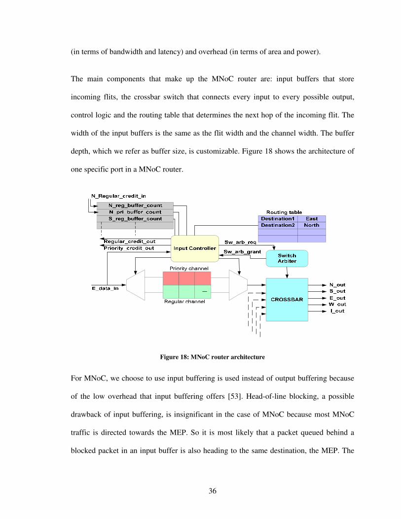
(in terms of bandwidth and latency) and overhead (in terms of area and power).
The main components that make up the MNoC router are: input buffers that store
incoming flits, the crossbar switch that connects every input to every possible output,
control logic and the routing table that determines the next hop of the incoming flit. The
width of the input buffers is the same as the flit width and the channel width. The buffer
depth, which we refer as buffer size, is customizable. Figure 18 shows the architecture of
one specific port in a MNoC router.
Figure 18: MNoC router architecture
For MNoC, we choose to use input buffering is used instead of output buffering because
of the low overhead that input buffering offers [53]. Head-of-line blocking, a possible
drawback of input buffering, is insignificant in the case of MNoC because most MNoC
traffic is directed towards the MEP. So it is most likely that a packet queued behind a
blocked packet in an input buffer is also heading to the same destination, the MEP. The

37
packet can be considered queued because its output port is busy and not because it is
blocked by another packet at the head of the queue. MNoC avails the advantage of low
overhead input buffers without affecting performance. Every input channel in the router
is multiplexed into two separate virtual channels, a priority channel and the regular
channel. The priority channel is used to exclusively transfer critical monitor data.
A packet that is injected into a network with a high priority (priority field in the packet
header is set to 1) enters the priority channel and travels in the same channel until it
reaches the destination. This channel is reserved exclusively for critical data and is not
used for regular data transfer. Effectively, packets remain in the channel determined at
packet injection. MNoC employs a credit based flow control to regulate data traffic and
to avoid packet dropping. To facilitate this, every router has buffer slot counters that keep
track of the number of empty buffer slots in the regular and the priority channels on the
adjacent routers. Traffic departs to the adjacent routers only when there is buffer space
available. The counter is incremented when buffer slots become available and vice-versa.
The availability of a buffer space is communicated by adjacent routers using credit
messages. Flits that enter the MNoC router are buffered in the appropriate input channel
and subsequently go through three router pipeline stages before reaching the next hop:
routing table look up, switch arbitration, and switch traversal.
In the routing table look up stage, the packet destination is used with a routing table to
determine the destination output port. Only the header flit goes through this pipeline
stage. The routing table can be simultaneously accessed by header flits from any number
of input channels. Hence, no arbitration is required at this stage. Once the destination

38
output port is known, the flit enters the switch arbitration stage. All types of flits go
through this pipeline stage, although the header flit is dealt with differently. Since MNoC
implements a wormhole routing approach, the header flit first gains access to the output
port and the port is then reserved until all flits in the packet reach the next hop. For the
header flit, the purpose of this stage is twofold. In the first phase, the flit sends a request
to the switch arbiter for access to the destination output port. If the output port is not
available, the header flit waits in the input buffer until it becomes available. If the port is
available, the header flit gains access to the port for the entire length of the packet. The
flit then enters the second phase where it sends a request for access to the crossbar switch
to enter the next router’s input port through the destination output port. The request is
sent, provided the buffer slot counter indicates the presence of a free buffer slot.
Otherwise, the flit waits in the queue until a buffer slot becomes available. Once switch
access is granted, the flit goes through the final pipeline stage where it traverses the
crossbar and enters the same channel (regular or priority) in the next router. The
corresponding buffer slot counter in the router is then decremented. Also, a credit
message is sent back to the previous router indicating that the flit has now moved out of
the input buffer. Since the output port is already reserved by the header flit, the body and
the tail flits only go through the second phase of the switch arbitration stage. The access
to the output port is released when the last flit (tail flit) leaves the port. The port can now
be claimed by a header flit from another packet. The priority channel is given preference
in the entire switch arbitration stage to ensure lowest possible latency on that channel.
Among requests from the regular channel, the arbiter grants access in a random fashion.

39
3.6 MNoC Router – Monitor Interface
Monitors in a system can either have dedicated interfaces to network routers or can
interface to the routers through shared buses or multiplexers. The interfaces need to be
generic and should allow for the interfacing of any kind of monitor to the network. The
control logic should be able to support both data push and data pull monitors. Also
synchronization issues that result out of different monitor and network frequencies need
to be addressed. In our architecture, the monitors and the network router connect through
a master-slave interface, the router end being the master and the monitor, a slave. The
architecture of the monitor-network interface is shown in Figure 19.
Figure 19 : MNoC monitor – network router interface
The interface control logic is built to read data at a pre-determined rate from the
connected monitors i.e. there is a control state machine at the router interface that
generates read addresses for each of the connected data pull monitors according to a pre-
set schedule. Also, any data pull type of monitor connected at the interface has a
dedicated interrupt line connected to the router interface and has a capability to generate a
interrupt indicating that it needs to be read. On the event of an interrupt, the controller
breaks away from the original sequence to generate a read address for the interrupting

40
monitor. It then returns back to the original schedule. Any data read from an interrupting
monitor is tagged as high priority data. Once the monitor data is read, the controller
appends it with information about the originating monitor and priority value. The data is
then written into the synchronizing FIFO which is read by the packetization module. The
synchronizing buffers act as frequency translators and the size of FIFO depends on the
difference between rate of production of the monitor data and consumption of data by the
network [22].
The packetization module converts the data to a format specified in 3.1.2 and forwards
the flits to the appropriate channel in the network (regular or priority), provided there is
space available in the buffers. In case the network is congested and the synchronizing fifo
is full the packetization module doesn’t accept any more data from the network interface.
The interface drops data from the monitors until the data is de-congested because only the
most recent data is relevant in a sensor network like MNoC.
3.7 Monitor Executive Processor – Network Interface
The MEP and the network router connect through a master-slave interface, the MEP
being the master and the router, a slave. A detailed view of the interface is shown in
Figure 20.

41
Figure 20 : MEP -Network interface
Monitor data received from either of the channels in the router is read by a de-
packetization module at the network router-MEP interface. Data is read from the regular
channel only if there is no data to service in the priority channel. The de-packetization
module has storage to hold flits until the entire packet arrives. It then reassembles the
packet, removes the routing information and forwards the monitor data along with the
source information into the synchronizing FIFO. The source information is required by
the MEP to identify the monitor from which the data originates. The synchronizing FIFO
also contains separate queues for regular and priority data. The MEP software should be
programmed to read information from the FIFOs at regular intervals by generating the
Read_req signal. Again, priority queue data is forwarded to the MEP by the interface
control module before data in the regular queue. The FIFO addresses synchronization
issues and is sufficiently sized to ensure that no data is dropped.
Once data is received, the MEP uses the source information to determine the type and
location of the monitor that sent out the data and takes necessary action by affecting
system parameters.

42
CHAPTER 4
MNoC VALIDATION APPROACH
In order to validate the MNoC approach and evaluate trade-offs for various design
constraints, such as area, bandwidth and latency, a series of synthesis and simulation
experiments have been performed. The efficiency of our monitor interconnect is assessed
for a multicore system using both an interconnect and a system-level architectural
simulator. The Popnet interconnect simulator [10] has been significantly modified to
estimate bandwidth and latency values for the heterogeneous MNoC interconnect. The
overhead of the monitor network-on-chip interconnect has been measured via hardware
synthesis. Finally, architectural simulations were performed using the SESC architectural
simulator [54] to quantify the benefits of employing MNoC at a system level. SESC is an
architectural multiprocessor simulator that models the power and performance of various
multi processor architectures. The power model that is integrated in the SESC is based on
Wattch [56] for processor architecture and CACTI [57] for caches. The temperature
model is based on Hotspot [58] that is called SESCSpot. SESCSpot, similar to Hotspot,
calculates temperature of the sub blocks based on the power trace of the architecture in a
post processing fashion.
4.1 MNoC Performance Evaluation
The bandwidth and latency evaluation of chosen MNoC configurations was performed
using a modified version of the Popnet simulator [10]. Popnet simulates traffic on a cycle
by cycle basis and gives an estimate of the average time (in terms of network clock
cycles) a packet takes to reach the destination. It simulates a mesh network with pipelined
virtual channel dynamic routers. Network parameters like network size, injection rate,

43
input buffer size, flit width and packet size are customizable. To rightly estimate the
performance of MNoC, popnet was modified to implement the MNoC protocols and
interfaces. Specific modifications and additions that were performed on the simulator are
listed below.
Popnet simulator originally implements a five stage router pipeline which we modified to
implement the MNoC three-stage router with priority channel support. The reduction in
the number of pipeline stages in the router leads to a reduction in the latency incurred by
a packet at a single hop and leads to an overall reduction in latency. The buffering
strategy at the router was modified to just input buffering instead of both input and output
buffering. This is because input buffering is more advantageous in the context on MNoC
as described in Section 3.5. The virtual channel arbitration stage originally present in the
popnet simulator was modified because MNoC packets are not required to go through
virtual channel arbitration as packets remain in the same virtual channel that they enter at
the time of injection. The simulator has also been extended to support expanded
interfaces for buses and multiplexers.
Popnet originally simulates a regular mesh network while monitors are distributed on the
chip in an irregular fashion. To enable the evaluation of realistic MNoC topologies, the
simulator was modified to support irregular topologies. This involves modifying the
address space of the routers and monitors, the number of input/output ports in the router
and the connections between routers. Also, Popnet implements an XY routing protocol
which is a preferred protocol for mesh networks due to its dead-lock free operation. XY
routing cannot be used for an irregular topology. Popnet was modified to support the

44
static distributed routing protocol described in Section 3.4. This involves changes in the
routing logic and addition of routing tables at every individual router in the network. The
paths from every router in the network to the MEP were generated using the deadlock
free routing algorithm [52] and the routing tables were populated with the generated
routes. The simulator, in modified form, allows for a complete evaluation of various
MNoC topologies and components.
4.2 MNoC Overhead Estimation
To estimate the overhead of our MNoC approach, we developed a synthesizable
hardware model of the MNoC router. The hardware model is parameterizable and allows
for evaluation of area for different router parameters. The hardware model was
synthesized using Synopsys Design Compiler using a 90nm standard cell library [55].
The input, output buffers at all the ports of the router are of customizable widths and
depths. The buffer width is same as the flit width and the physical link width. Reducing
this negatively impacts the performance of the network but offers an area saving. Similar
is the impact while reducing the buffer depth. The control logic in the router, the routing
table and the crossbar switch also add a fixed amount of area overhead. The routing logic
that determines the next hop of a flit by looking up the routing table, the switch arbiter
that controls access to the crossbar, and the output control logic that reads credit
messages and controls traffic on the physical channel are components of the control logic.
The synchronizing buffers, packetization modules and the control logic at the interfaces
also contribute to the overhead of MNoC. A hardware model of the interfaces was
created to estimate the overhead. Results from hardware synthesis of MNoC for specific
systems are presented in Section 5.

45
Assuming that the physical links between routers can be traversed in one clock cycle, the
frequency at which the routers operate dictates the frequency of the entire network. The
maximum bandwidth of the router is a product of the router frequency and router width
(same as the flit width). The router hardware is pipelined, as described in Section 3.5 , to
allow for high frequency operation. The hardware model created for the area estimation
was used to assess the maximum frequency of the router.
4.3 MNoC System Level Validation
Our generic approach to system level MNoC validation is shown in Figure 21.
Identify and build parameterizable MNoC
components
Building MNOC
Infrastructure
Validate
MNOC for sample
monitoring systems
Simulate , using Popnet simulator, a suitable topology with monitor layout information
Parameter tuning for different area and performance
values
Assess system level design constraints
using SESC and area
constraints using the hardware model
MonitoringRequirements
(latency, BW, area, power)
Figure 21 : MNoC validation approach
In general, for any specific monitoring system, the network components for MNoC
should be chosen and sized in a way that satisfies system bandwidth and latency
requirements with a minimal resource overhead. The latency and bandwidth requirements
depend largely on the type of monitor and the reaction that the MEP takes in response to
monitor data. As described in Section 4.1, the network performance of the chosen MNoC
topology can be estimated using the modified Popnet simulator. The overhead can be

46
estimated using our hardware model. A system level architectural simulation can then be
performed to ensure that the latency and bandwidth provided by MNoC are sufficient and
allow the MEP to react to monitor data in a timely fashion. Mismatches can be corrected
by tuning the network parameters and re-evaluating the network performance and
overhead. Timely MEP reaction translates to a quantifiable system level benefit that can
be measured using the architectural simulation.

47
CHAPTER 5
EXPERIMENTAL APPROACH AND RESULTS FOR VALIDATING MNOC
To test our Network on Chip approach for monitors, we have identified some sample
systems which will benefit from such an approach. These systems are representative of a
larger set of monitoring systems that MNOC can cater to. This section describes two
sample systems and MNoC’s application for these systems.
5.1 Thermal Management Using MNoC
Contemporary processors use around 10-25 thermal sensors per core [9] and as the
number of cores on a die increase we can foresee the need of collating data from a large
number of thermal monitors from across the chip. Using point to point connections for
such a large number of monitors to a centralized controller with a low resource overhead
is not a feasible task. Also, connecting such a large number of monitors to a bus
significantly degrades the performance of the bus. So from a scalability standpoint, a
MNoC like network becomes essential although the actual bandwidth required by thermal
monitors is considerably less. For a chip temperature gradient of 60degC/sec and a
precision of 1.2 degC , it suffices to sample the thermal monitor once every 20ms [6].
Assuming a 12 bit data to be transported at this sampling rate, the monitor bandwidth is
around 0.6 Kbps.
To evaluate the benefits of MNoC in a system that processes thermal information, we
perform an interconnect and system-level simulation of a thermal monitoring system on
an 8 core processor. The goal of the experiment is to use MNoC for collating temperature
data from a group of thermal monitors spread across cores and to perform dynamic

48
frequency scaling (DFS)[59] if preset thermal thresholds are exceeded. The delays
associated with MNoC were simulated using the modified Popnet simulator. SESC was
used for the system level simulation which involves generating thermal data and
simulation of the MEP that performs dynamic frequency scaling.
In this experiment, 24 thermal monitors on each of the 8 processor cores report
temperature values from various locations on the chip. The processor cores used here are
based on the AMD Athlon 64 processor [60]. The layout of the eight core system is
shown in Figure 22. There are two MNoC routers per core, each of which collects
thermal data from 12 thermal monitors using a multiplexer. Thus 192 thermal monitors
from eight cores connect to 16 routers through 16 multiplexers. Since thermal monitors
can be classified as low bandwidth data pull monitors, low bandwidth multiplexer
connections were used. The MEP is attached to a dedicated router as seen in Figure 22.
Figure 22 : Monitor network on chip layout for thermal monitors on an 8 core processor

49
The MEP was placed at a central location to the routers. The resultant network topology
is an irregular mesh which is effectively a regular 5x5 mesh with missing routers and
links. A dummy router adjacent to the MEP was added to facilitate routing. Without this
router, some of the routers must be marked as deactivated nodes which are not reachable
[52]. With this 18 router setup, the deadlock-free routing algorithm [52] was used to
generate paths from every router to the MEP. Each of the 18 routers can be addressed
using 5 bits, so the message destination field is 5 bits wide. The actual temperature values
are 12 bit wide. An additional 8 bits are required to identify the origin of the data from
among the 192 monitors.
5.1.1 Interconnect simulation results
Our modified interconnect simulator was used to evaluate the behavior of the above
described network for different network parameters. Figure 23 shows a plot of network
latency versus injection rates for various router buffer sizes. The value on the X axis,
cycles between injections, indicates the number of clock cycles between two sampling
points for the thermal monitors Network latency (the Y axis) indicates the time required
(in clock cycles) for data to travel from a monitor to the MEP. Figure 24 shows the same
plot for the priority channel. We simulated 5% of the total traffic to be priority traffic to
assess the latency on the priority channel. It is clear from the plot that the latency on this
channel is more or less constant and is ideally suited for low latency critical data transfer.
There is practically no impact of buffer sizes on the latency. Figure 23 indicates a
significant dependence for the regular channel on the input buffer size for sizes less than
4. For buffer sizes greater than and equal to 4, limited latency reduction is achieved by

50
increasing buffer size. For longer cycles between injections, the regular channel latency
becomes insensitive to buffer sizes.
Regular channel latencies for different buffer sizes and
data width = 12
0
2000
4000
6000
8000
10000
12000
0 200 400 600 800 1000 1200
Cycles between injection
Netw
ork
late
ncy
(Clk
cycle
s)
100
16
12
8
6
4
3
2
Buffer
Buffer size
Figure 23 : Regular channel latencies for different buffer sizes
Figure 25 shows a plot of network latency versus injection rate, for different flit widths.
As we can see from the plot, for very low sampling rates (cycles between injection >
800), the latency becomes independent of the flit width. For higher sampling rates, the flit
width that gives ideal latency increases with increasing cycles between injections.
Priority channel latencies for different buffer sizes and
data width = 12
0
5
10
15
20
25
0 200 400 600 800 1000 1200
Cycles between injection
Netw
ork
late
ncy
(Clk
cycle
s)
100
16
12
8
6
4
3
2
Buffer size
Figure 24 : Priority channel latencies for different buffer sizes

51
Regular channel latencies for different data widths for buffer
size = 4
0
1000
2000
3000
4000
5000
6000
0 100 200 300 400 500 600 700 800 900 1000 1100
Cycles between injection
Netw
ork
late
ncy
(C
lk c
ycle
s)
11
12
14
16
18
20
Data width
Figure 25 : Regular channel latencies for different flit widths
Overall, it can be inferred from the results that for higher cycles between injection (lower
sampling rates and hence lower required bandwidths), the latency values are mostly
insensitive to network parameters like buffer size and flit widths. Adding more resources
adds overhead but yields little benefit. At such low sampling rates, like in the case of
thermal monitors, close to ideal network latency can be achieved with minimal network
resources. Monitors with higher sampling rates have latencies that are highly network
dependent. These monitors usually dictate the choice of network parameters.
5.1.2 Hardware estimation results
While the interconnect simulation provides an insight into the network performance with
varying parameters, the hardware estimates from Table 2 are essential to evaluate to
ensure that the network overhead is within system design constraints. 17% of the total
resources are consumed by the network interfaces and the remaining 83% is consumed by
the network itself. Of the total network resources, 35% is consumed by control logic,

52
49% by input buffers in the routers and the remaining 16% is consumed by switches,
routing tables etc.
Flit width Buffer size
Total MNoC area at
90 nm in mm2
12 2 0.700
14 2 0.765
16 2 0.825
18 2 0.890
20 2 0.950
12 4 0.819
14 4 0.894
16 4 0.970
18 4 1.043
20 4 1.116
12 8 1.084
14 8 1.201
16 8 1.314
18 8 1.420
20 8 1.530
12 16 1.571
14 16 1.751
16 16 1.919
18 16 2.094
20 16 2.262
Table 2 : MNoC area results
5.1.3 Architectural simulation results
In this section we demonstrate how an MNoC configuration that satisfies system design
constraints while providing a performance benefit can be constructed using results from
the interconnect simulation and hardware estimations. We use SESC to simulate eight
processors and one central MEP, as seen in Figure 22.
In this experiment, the 192 thermal monitors on the 8 core chip were sampled every 2ms
to provide a resolution of 0.1 degC. This number was determined assuming a maximum

53
temporal temperature gradient of 60degC/sec [6]. To meet this bandwidth requirement,
an MNoC configuration with flit size of 12 bits and an input buffer size of 4 was used.
The resulting MNoC area from Table2 is 0.819 mm2. The temperature reported by the
monitors is collected by MNoC and transported to the MEP which uses the data for
dynamic frequency scaling.
Dynamic frequency scaling of a processor system improves system performance by
operating cores within power dissipation and temperature limits. Two experiments were
performed on the 8 core system to demonstrate the benefits of DFS on a benchmark
application. A floating point benchmark called Whetstone [61] is used to conduct the
experiments for a total of 450M instructions per processor. In one scenario, the system
was operated at a constant frequency of 500MHz to meet pre-defined power and
temperature limits and the run time consumed was noted. In this case since the predefined
temperature threshold is not exceeded, it was not necessary to employ MNoC. This is a
non-MNoC system. In a second scenario, MNoC is employed to transport thermal
monitor data which is used by a MEP to perform DFS. In this case, the operating
frequency of the system is toggled between 1 GHz and a lower frequency to ensure that
the specified power and temperature limits are not violated. The run time was again noted
and the resulting performance improvement was calculated. It was noted that MNoC
gives a 33% performance benefit for the 8 core system. To evaluate how the
performance benefit using MNoC scales with the number of cores, we also performed
experiments for 2 core, 4 core, and 12 core systems. The results obtained for various
system configurations are shown in Table 3. The advantage of employing MNoC
becomes is visible for all core configurations

54
Freq = 500MHz
(90nm)
Freq = 1000
MHz + DFS
(90nm)
Cores
Run Time
Run Time
Performance
benefit
due to
MNoC
2 3.36 sec
2.42 sec
28 %
4 2.75 sec
2.25 sec
18 %
8 2.27 sec
1.52 sec
33 %
12 1.75sec
1.35 sec
23 %
Table 3 : Runtimes for MNoC and non-MNoC cases
Also, assuming an area of 378mm2 for a 90nm 8 core processor [45], we obtain the area
overhead of MNoC to be 0.819/378 = 0.21%. The SESC simulation results illustrate that
the chosen MNoC configuration allowed an implementation of the DFS scheme which
resulted in a performance benefit versus the non-MNoC case. The network overhead is
also a meager 0.21%.
5.2 Voltage Droop Management Using MNoC
As power supply voltages and associated noise margins continue to decrease, the control
of power supply voltage is becoming increasingly important for system performance and
reliability. Recently, voltage droop or dI/dt events are becoming serious concerns in high
performance processor designs. They are usually addressed by expensive packaging
techniques [47]. This experiment involves the use of real time monitoring and control
techniques that use MNoC to offset voltage drops at system run time. This approach to
dynamically handling voltage droops effectively reduces the complexity and cost of
building expensive packaging solutions.

55
Critical path delay monitors are used to identify failing paths in the circuit which are
indicative of increasing temperature, wear-out or voltage droop. The critical path monitor
described in Section 2.1.3 will be used for experiments pertaining to this section. We
however assume that the most significant impact on the critical path delay is caused by a
voltage droop event. We particularly target the second and third kind of droops as
defined in [3]. The high bandwidth and low latency offered by MNoC enables such a real
time droop monitoring design.
The monitoring setup involves 8 delay monitors per core [7] which report digitized delay
values in 12 bits of data. This data will be transported to the MEP through MNoC. Since
delay values can potentially change every clock cycle, the monitors ideally need to be
sampled every clock cycle. Hence unlike the thermal monitors, the delay monitors require
very high bandwidth on the network. In response to a voltage drop event, we can either
increase the voltage or reduce the frequency of the core to enable correct operation of the
system. We simulated two different MNoC systems, one in which the MEP responds by
reducing the frequency of the core and another in which the MEP increases the voltage of
the core to avoid a serious voltage droop. Results provided in this section indicate that the
MNoC based systems provide a power or performance benefit compared to a system that
doesn’t employ MNoC. In a non MNoC system, the voltage or frequency needs to be set
to a highly conservative value that accounts for the worst case voltage droop. In contrast,
MNoC enables a better than worst case design rather than building systems that handle
worst case possibilities which are very rare in real workloads.

56
5.2.1 Modifying voltage in response to voltage droop
Figure 26 details out our approach to countering a single voltage droop using MNoC. The
system requires cores to be operating at a voltage of 1.2Volts. Assuming a maximum
voltage droop of 20% , a supply voltage of 1.2V can reduce to 0.96V in the worst case.
This voltage is not sufficient to keep the core running at its original frequency. This is
due to the exponential dependence of circuit frequency on supply voltage as obtained
from [16]. In the event of a voltage droop, the delay monitors indicate an increase in
critical path delay. This information is transported to the MEP in a timely fashion using
MNoC, which then increases the supply voltage. This is in contrast to a non-MNoC case
where the voltage needs to be set to 1.4V (1.16 V + 20% of 1.2V, since the timing delays
between 1.16V and 1.2 V are almost insignificant) to account for the worst case droop in
the system. This less conservative approach to dealing with voltage droop leads to a
power savings when compared to the non MNoC case.
Voltage vs Time
1.1
1.15
1.2
1.25
1.3
1.35
0 50 100 150 200 250 300 350 400 450 500 550
Time in ns
Vo
ltag
e in
Vo
lts
Core voltage
Supply voltage
1) Voltage begins to drop
at 150ns
2) Voltage monitor sampled
at 200ns 3) Sampled value reaches MEP
through MNoC after 50ns @ 250ns
4) MEP initiates an increase in supply voltage
and this is visible after a small VRM delay
5)Voltage continues to drop and is
resampled at 300ns
6) Supply voltage is increased again to
counter the drop sampled at 300ns
7) Drop effect is not visible from
the sample at 400ns. So supply
voltage is changed back to normal
Figure 26 : Single droop recovery using MNoC

57
It should however be noted that it takes a finite amount of time to detect, communicate
and react to a change in the critical path delay. The initial supply voltage should account
for the amount of voltage droop that can occur before any action can be taken. So the
initial supply voltage in the MNoC case is dictated by the delay in sampling the monitor,
MNoC delay and the voltage regulator settling time. With larger sampling times or
communication delays, the initial voltage to be set could be close to the worst case
voltage of 1.4 V. Table 4 gives an insight into how the initial supply voltage can vary
with increasing sampling intervals and MNoC delays on an 8 core processor. For small
sampling intervals3, the MNoC delay is very high due to congestion. For higher sampling
intervals, the MNoC delay is very low but the fact that we are sampling less often
compensates for the lower MNoC delay. Specific combinations of sampling intervals and
MNoC delays that yield a power benefit were determined experimentally and the results
are reported in the following sections. Assuming any voltage less than 1.16 V is
catastrophic, we arrive at the generic equation used to calculate the initial voltage as
shown below;
New voltage = Voltage droop rate *(Sampling interval + MNoC delay + voltage regulator
delay ) * Network clock period + 1.16V
A network clock frequency of 510 MHz is used as determined from synthesis of the
network router. The voltage regulator delay also plays a significant role in determining
the initial voltage. The following section summarizes the assumptions made in this
experiment regarding the voltage regulator settling time.
3 Sampling interval is the time between two samples of the delay monitor

58
Assumptions regarding voltage regulator settling time
Traditional off chip voltage regulators use bulky inductors and capacitors which require
that the voltage regulator modules be separate off-chip components. These off-chip
voltage regulators typically have very slow transition rates of the order of micro seconds
[12]. Dynamic voltage and frequency scaling techniques [35] benefit systems by
modifying voltage and frequency at run time so as to maximize performance while
operating within specific power limits. The slow transition rates of off-chip voltage
regulators have limited the benefits of dynamic voltage and frequency scaling techniques
[13]. To take most advantage of the benefits of DVFS, there has been interest in building
on chip voltage regulators that avoid the need for bulky capacitors and inductors and
enable voltage regulator transition times of the order of nanoseconds [13, 65].
For this experiment we consider an on-chip voltage regulator [13] that has transition rates
of the order of nanoseconds and can vary voltage on a per core basis. The voltage
regulator described in [13] is designed to operate at higher switching frequencies that
enable it to switch voltages rapidly. The higher switching speeds however entail higher
voltage regulator power than regular off chip voltage regulators. On chip voltage
regulators need to be designed with minimal overhead in a way that these contrasting
requirements are traded off.

59
Monitor sampling
interval ( Clock cycles)
MNoC Delay ( Clock cycles) Voltage (V)
130 254.22 1.463
140 10.49 1.276
150 9.50 1.283
160 11.20 1.292
170 12.40 1.301
180 11.45 1.309
190 10.00 1.316
200 9.49 1.323
210 9.49 1.331
220 10.36 1.340
230 12.00 1.349
Table 4 : Variation of initial supply voltage for the MNoC based system as the monitor sampling
rates vary
Experiments to determine power savings were conducted on 4, 8 and 16 core processors
with a 9 router MNoC setup. One of the routers has a dedicated connection to the MEP
while the rest of the 8 routers connect to delay monitors through a multiplexer interface.
The network size remains the same as the number of cores increase. Effectively, the
number of monitors attached to each router increases as the number of cores increase.
The floating point benchmark Whetstone [61] was used to conduct the voltage droop
experiments. The interconnect simulator was used to estimate MNoC delays and SESC
was used to obtain the power trace of the application. A flit width of 16 and a buffer size
of 4 were chosen for the experiments. In an offline process, the voltage modifications
were applied on the power trace and the total power savings were calculated against the
non MNoC case. In the non MNoC case, the voltage for the entire run of the benchmark
was set to the worst case voltage of 1.4 volts. The percentage power savings recorded for
the 4 core, 8 core and the 16 core versions are shown in Figure 27, Figure 28, and Figure
29 respectively.

60
Power savings with MNoC on a 4 core processor
-15
-10
-5
0
5
10
15
20
30 40 50 60 70 80 90 100 110 120 130 140 150 160 170 180 190 200 210 220
Cycles between sampling of monitor
Perc
en
tag
e p
ow
er
savin
gs
Figure 27 : Power savings with MNoC on a 4 core processor
Power savings with MNoC on a 8 core processor
-15
-10
-5
0
5
10
15
70
80
90
10
0
11
0
12
0
13
0
14
0
15
0
16
0
17
0
18
0
19
0
20
0
21
0
22
0
23
0
24
0
25
0
26
0
27
0
28
0
29
0
30
0
Cycles between sampling of monitor
Pe
rce
nta
ge
po
we
r s
av
ing
s
Figure 28: Power savings with MNoC on a 8 core processor
Power savings with MNoC on a 16 core processor
-15
-10
-5
0
5
10
140 150 160 170 180 190 200 210 220 230 240 250 260 270 280 300 320
Cycles between monitor samples
Pe
rce
nta
ge
po
we
r s
av
ing
s
Figure 29 : Power savings with MNoC on a 16 core processor

61
As seen from the results, all three configurations result in power savings against the non
MNoC case for specific combinations of sampling rates and MNoC delays. But for a
given size of the network and a given bandwidth, the four core version has the best
savings. As number of cores increase the number of monitors increases, requiring more
bandwidth from the network. This type of trend clearly motivates the need for a scalable
medium like MNoC as against buses or serial links. The increase in power savings on a
16 core processor as the bandwidth of the network increases is shown in Figure 30. The
bandwidth of the network was increased by increasing the width of the router (same as
increasing the flit width). As expected, the highest bandwidth network yields maximum
power savings.
It can also be noticed from the results that certain values of sampling intervals yield a
negative benefit in terms of power. This is because the sampling or the network delays
are so high that the system gains no benefit from run time monitoring. Clearly, these
combinations of sampling intervals and MNoC delays will have to be avoided.
Power savings with increasing MNoC bandwidth on a 16 core processor
-15
-10
-5
0
5
10
15
130 140 150 160 170 180 190 200 210 220 230 240 250 260 270 280
Cycles between sampling of delay monitors
Pe
rcen
tag
e
po
wer
sav
ing
s
BW
2*BW
4*BW
Figure 30: Power savings with increasing MNoC bandwidth on a 16 core processor

62
The percentage of power savings is also dependent on router components like buffer sizes
which can significantly influence MNoC delays. Figure 31 shows the power savings as
the buffer sizes in the individual routers are modified. The trend indicates that increasing
the buffer sizes beyond a buffer size of 8 doesn’t cause any significant improvement in
the power savings encouraging the use of smaller buffer sizes.
Variation in power savings in a 8 core processor with varying buffer sizes
-20
-15
-10
-5
0
5
10
15
120 130 140 150 160 170 180 190 200 210 220 230 240 250 260 270 280 290 300
Cycles between sampling of the delay monitor
Pe
rce
nta
ge
po
we
r s
av
ing
s
4
8
12
16
Buff
size
Figure 31: Variation in power savings with variable MNoC buffer sizes
Increasing the bandwidth of the network and using larger input buffers leads to an
increase in the MNoC overhead. It is necessary to quantify the area of MNoC to
effectively tradeoff system level MNoC benefits with the overhead incurred. Table 5 and
Figure 32 give an estimate of the overhead of MNoC for the 9 router configuration.

63
Flit width Buffer size Total MNoC area (mm2)
BW = B 16 4 0.484
16 8 0.657
16 12 0.805
16 16 0.959
BW = 2B 32 4 0.663
32 8 1.098
32 12 1.351
32 16 1.650
BW = 4B 64 4 1.375
64 8 1.983
64 12 2.493
64 16 3.028
Table 5: MNoC area estimates for the 9 router configuration
MNoC area with increasing network bandwidth
0
0.5
1
1.5
2
2.5
3
3.5
4 8 12 16
Input buffer sizes
Are
a o
f M
No
C i
n m
m2
BW
2*BW
4*BW
Figure 32 : Quantifying MNoC area overhead
5.2.2 Modifying frequency in response to voltage droop
Another alternative to countering voltage droop is to reduce the frequency of the core in
the event of a droop. This experiment was conducted on similar lines as the voltage
modification experiment. It was assumed that the cores could operate at a frequency of
1GHz at a voltage of 1.2 V. In case of a worst case drop, the voltage can reduce to 0.96V

64
in which case the core cannot operate at a frequency higher than 0.66 GHz. This value
was again obtained using the dependence of circuit frequency on supply voltage as
obtained from [16]. The initial frequency depends on the sampling interval, MNoC delay
and the time its takes for the frequency change to take effect
Assumptions regarding frequency transition rates
Frequency transition rates are quicker than voltage transition rates and can be of the order
of a few nanoseconds [67]. Also, a clock system that enables fast frequency
modifications without PLL re-lock penalties is described in [66]. Enabling rapid, per core
frequency scaling benefits the MNoC assisted system in terms of performance. Table 6
indicates how the initial frequency of the cores can vary with increasing sampling
intervals and MNoC delays. Higher frequency transition rates require that the initial
frequency shown in Table 6 be set more conservatively.
Sampling interval (
Clock cycles)
MNoC Delay ( Clock cycles) Frequency(Ghz)
90 104.17 0.769
110 10.49 0.885
120 12.00 0.868
130 9.49 0.852
140 9.49 0.836
150 13.22 0.820
160 11.54 0.805
170 9.49 0.790
180 9.49 0.775
190 9.49 0.761
Table 6 : Variation of initial frequency for the MNoC based system as the monitor sampling rates
vary

65
Experiments to estimate the performance benefit of using MNoC were conducted on 4, 8
and 16 core processors with a setup of 9 routers. The floating point benchmark
Whetstone [61] was again used to conduct the voltage droop experiments. The
interconnect simulator was used to estimate MNoC delays and SESC was used to obtain
the run-time trace of the application. In an offline process, the frequency modifications
were applied on the power trace and the total run-time savings were calculated against the
non MNoC case. In the non MNoC case, the frequency for the entire run of the
benchmark was set to the worst case frequency of 0.66 GHz. The percentage performance
savings recorded for the 4 core, 8 core and the 16 core versions are shown in Figure 33.
Performance benefit with varying MNoC bandwidth is indicated in Figure 34. The trends
are similar to those noticed in Section 5.2.1
Performance benefit in multicores using MNoC
-15
-10
-5
0
5
10
15
20
25
30
30 50 70 9011
013
015
017
019
021
0230 250 27
030
0
Cycles between sampling of the delay monitors
Pe
rce
nta
ge
pe
rfo
rma
nc
e b
en
efi
t
4 cores
8 cores
16 cores
Figure 33: Performance benefit in multi-cores using MNoC

66
Performance benefit with varying bandwidth on a 16 core processor that uses
MNoC
-15
-10
-5
0
5
10
15
130 140 150 160 170 180 190 200 210 220 230 240 250 260 270 280
Cycles between injection of delay monitor
Pe
rce
nta
ge
pe
rfo
rma
nc
e
be
ne
fit
BW
2*BW
4*BW
Figure 34: Performance benefit with varying MNoC bandwidth
Overall, the experimental results from this section indicate that the high bandwidth and
low latency offered by MNoC enable a run time adaptation of voltage/frequency that
yields close to 20% improvement in power/performance compared to a non MNoC
system.

67
CHAPTER 6
CONCLUSIONS AND FUTURE WORK
This thesis presents a scalable and lightweight interconnect approach for monitor
connections. We developed the necessary infrastructure to test the performance and
evaluate the overhead of various network configurations and topologies. Our
parameterizable network solution allows for the development and assessment of various
design trade-offs for on-chip monitoring systems. The approach is validated by
demonstrating the performance benefits obtained on a multicore processor system that
uses a MNoC based thermal monitoring system. Also, when employed to transport
information on a delay monitoring system, MNoC provides enough bandwidth and
latency to allow the MEP to adjust voltage/frequency in response to voltage droops at run
time. This is in contrast to statically setting conservative voltage and frequency values.
This leads to an overall power/performance benefit in the system compared to a non-
MNoC design.
In the future, automation of MNoC design for a given set of monitors and design
constraints is a promising area that needs to be addressed. We can examine the possibility
of using the regular network on chip used for data communication to also transport
monitor traffic. We can also look at using MNoC to locally collaborate or aggregate
monitor data. This can reduce the overall traffic on the network and could require lesser
network resources. Another interesting area of work is the software associated with the
MEP. Innovative circuit level techniques for MNoC wire fabric can also help scalability
and low latency.

68
BIBLIOGRAPHY
[1] L. Benini and G. De Micheli, “Networks on Chips: a New SoC Paradigm,” IEEE
Computer , vol. 35, no. 1, January 2002, pp. 70 -78
[2] W. J. Dally and B. Towles, “Route Packets, Not Wires: On-Chip Interconnection
Networks,”, In Proceedings of the 38th
Design Automation Conference, June 2001,
Las Vegas, NV
[3] K.L Wong, T. R. Arabi, M. Ma, G. Taylor , “Enhancing microprocessor immunity to
power supply noise with clock-data compensation”, IEEE Journal on Solid State
circuits , vol. 41, no 4, Apr 2006 , pp. 749 - 758
[4] W. Webb. Take the heat: Cool that hot embedded design. Technical Report, EDN,
May 2004. http://www.edn.com/article/CA415105.html
[5] S. Velusamy, W. Huang, J. Lach, M. Stan, and K. Skadron, “Monitoring Temperature
in FPGA based SOCs” , In Proceedings of the International Conference on Computer
Design, Oct 2005, San Jose, CA
[6] R. McGowen, C. A. Poirier, C. Bostak, J. Ignowski, M. Millican, W.H. Parks, S.
Naffziger, “Power and Temperature Control on a 90nm Itanium Family Processor”,
IEEE Journal on Solid State circuits , vol. 41, no 1, Jan 2006 , pp. 229-237
[7] M.S. Floyd, S. Ghiasi, T.W Keller, K. Rajamani, F.L. Rawson, J. C. Rubio, M. S.
Ware, “ System Power Management Support in the IBM Power6 Microprocessor” ,
IBM Journal of Research and Development, vol. 51, no 6, Nov 2007
[8] D. Brooks and M. Martonisi, “Dynamic Thermal Management for High-Performance
Microprocessors”, In Proceedings of the 7th
International Symposium on High
Performance Computer Architecture, Jan 2001, Nuevo Leone, Mexico
[9] R. Mukherjee, S. O. Memik, “Systematic temperature sensor allocation and
placement for microprocessors”, In Proceedings of the 43rd
ACM IEEE Design
Automation Conference, July 2006, San Francisco, USA
[10] L. Shang, L.S. Peh, N. K. Jha, “Dynamic voltage scaling with links for power
optimization of interconnection networks”, In Proceedings Of the International
Symposium on High-Performance Computer Architecture, Anaheim, CA, Feb 2003
[11] W.J. Dally, C.L. Seitz, “Deadlock-free adaptive routing in multiprocessor
interconnection networks”, In IEEE Transactions of Parallel and Distributed Systems,
Vol 4, no 4, pp 466-475
[12] L. T. Clark, E. J. Hoffman, J. Miller, M. Biyani , L. Luyun , S. Strazdus , M. Morrow
, K. E. Velarde ,M. A. Yarch ,"An Embedded 32-b Microprocessor Core for Low-

69
power and High-performance applications ", In IEEE Journal of Solid State
Circuits,Vol 36, no.11, pp 1599-1608
[13] W. Kim, M. Gupta, G. Y. Wei, D. Brooks, “System Level Analysis of Fast, Per-Core
DVFS using On-Chip Switching Regulators,” In Proceedings of the 14th International
Symposium on High-Performance Computer Architecture, February 2008, Salt Lake
City, UT
[14] S. Tam, J. Leung, R. Limaye, S. Choy, S. Vora, M. Adachi, “Clock Generation and
Distribution of a Dual-Core Xeon Processor with 16MB L3 Cache”, IEEE ISSCC
Tech. Digest, 2006
[15] J. Smolens, B. Gold, J. Kim, B. Falsafi, J. Hoe, and A. Nowatzyk, “Fingerprinting:
Bounding Soft Error Detection Latency and Bandwidth,“ In Proceedings of the
International Symposium on Architectural Support for Programming Languages and
Operating Systems, Oct 2004, Boston, MA
[16] A. Laffely, J. Liang, R. Tessier, and W. Burleson, “ Adaptive System on a Chip: A
Backbone for Power-Aware Signal Processing Cores,” In Proceedings of the IEEE
Conference on Image Processing, September 2003, Barcelona, Spain,
[17] B. R. Quinton, S. J. E. Wilton, “Post-Silicon Debug using Programmable Logic
Cores”, In Proceedings of the IEEE Conference on Field Programmable Technlogy,
Dec 2005, Singapore.
[18] T. Wolf, S. Mao, D. Kumar, B. Datta, W. Burleson, and G. Gogniat. “Collaborative
Monitors for Embedded System Security”. In Proceedings of the First International
Workshop on Embedded Systems Security, October 2006, Seoul, South Korea
[19] S. Shyam , K. Constantinides , S. Phadke , V. Bertacco , T. Austin, “Ultra Low-Cost
Defect Protection for Microprocessor Pipelines”, In Proceedings of the 12th
International Conference on Architectural Support for Programming Languages and
Operating Systems, Oct 2006, San Jose , CA
[20] A. Drake, R. Senger, H. Deogun, G. Carpenter, S. Ghiasi, T. Nguyen, N. James, M.
Floyd, V. Pokala, “ A Distributed Critical-Path Timing Monitor for a 65nm High-
Performance Microprocessor “, In Proceedings of the IEEE International Solid-State
Circuits Conference , Feb 2007
[21] R. Maro, Y. Bai, R.I. Bahar , “Dynamically Reconfiguring Processor Resources to
Reduce Power Consumption in High-Performance Processors,” In Proceedings of the
First International Workshop on Power-aware Computer Systems – Revised Papers,
2000
[22] T. Chelcea, S.M. Nowick, “Robust Interfaces for Mixed-Timing Systems “, IEEE
Transactions On VLSI Systems, vol. 12, no. 8, Aug 2004

70
[23] P. Gurrier and A. Greiner , “A Generic Architecture For On-chip Packet-Switched
Interconnections”, In Proceedings of the Design Automation and Test in
Europe(DATE) Conference, March 2000, Paris, France
[24] T. Bjerregaard and S. Mahadevan, “A Survey of Research and Practices of Network-
on-Chip”, ACM Computing Surveys, vol. 38, no.1, March 2006
[25] W. J. Dally, “Virtual-Channel Flow Control.” IEEE Transactions on Parallel and
Distributed Systems, vol. 3, no. 2, 1992, pp. 194–205.
[26] M. B. Taylor, J. Kim, J. Miller, D. Wentzlaff, F. Ghodrat , B. Greenwald , H.
Hoffman, P. Johnson , J.W. Lee, W. Lee, A. Ma , A. Saraf , M. Seneski, N.
Shnidman, V. Strumpen , M. Frank , S. Amarasinghe ,and A. Agarwal, “The RAW
microprocessor: A computational fabric for software circuits and general-purpose
programs”, IEEE Micro, vol. 12, no. 2, 2002, pp. 25–35.
[27] M. Saen, K. Osada, S. Misaka, T. Yamada, Y. Tsujimoto, Y. Kondoh, T. Kamei,
Y. Yoshida, E. Nagahama, Y. Nitta, T. Ito, T. Kameyama, N. Irie, “ Embedded SoC
Resource Manager to Control Temperature and Data Bandwidth ”, In Proceedings of
the Solid-State Circuits Conference, Feb 2007, San Francisco, CA
[28] S. Velusamy, W. Huang, J. Lach, K. Skadron , “Monitoring Temperature in FPGA
based SoCs” , University of Virginia , CS Technical Report , CS-2004-39
[29] K. Goossens , J. Dielissen , AND A. Radulescu, “ Æthereal network on chip:
Concepts, Architectures and Implementations”, IEEE Design and Test of Computers ,
Vol. 22,no. 5, Sep-Oct 2005, pp. 414–421
[30] I. Cidon and I. Keidar, “Zooming in on Network-on-Chip Architectures”, CCIT
research report, Technion University, Haifa, Israel, December 2005.
[31] E. Chi , A. M. Salem, R.I. Bahar, R. Weiss, “Combining Hardware and Software
Monitoring for Improved Power and Performance Tuning”, In Proceedings of the
Seventh Workshop on Interaction between Compilers and Computer Architectures ,
Anaheim, CA, Feb 2003
[32] D. Ernst, S. Das, S. Lee, D. Blaauw, T. Austin, T. Mudge, N. S. Kim, K. Flautner,
"Razor: Circuit-Level Correction of Timing Errors for Low-Power Operation", IEEE
Micro, vol. 24, no. 6, Nov/Dec, 2004, pp. 10-20
[33] E. Boemo and S. Lopez-Buedo, “Thermal Monitoring on FPGAs using Ring-
Oscillators”, In Proceedings of the Seventh International Workshop on Field
Programmable Logic and Applications , Sep 1997, London, UK

71
[34] K. Skadron, M. R. Stan, W. Huang, S. Velusamy, K. Sankaranarayanan, and D.
Tarjan, “Temperature-Aware Microarchitecture”, In Proceedings of the Thirtieth
International Symposium on Computer Architecture, June 2003, San Diego, CA
[35] P. Macken, M. Degrauwe, M. Van Paemel, H. Oguey , "A voltage reduction
technique for digital systems," Digest of Technical Papers Solid-State Circuits
Conference , Feb 1990, pp.238-239
[36] P. P. Shirvani, N. R. Saxena, E. J. McCluskey, “Software-Implemented EDAC
Protection Against SEUs” , IEEE Transactions on Relability, Vol. 49, no. 3, 2000, pp.
273-284
[37] S. Naffziger, “Dynamically Optimized Power Efficiency with Foxton Technology”,
Hot Chips 2005, Stanford University, Palo Alto, CA
[38] A. Hemani, A. Jantsch, S. Kumar, A. Postula, J. Oberg, M. Millberg, and
D.Lindqvist, “Network –on-Chip : An Architecture for Billion Transistor Era”, In
Proceedings of the IEEE NorChip Conference, Nov 2000, Turku, Finland
[39] S. Kumar, A. Jantsch, J.P. Soininen , M. Forsell, M. Millberg , J.Oberg, K. Tiensyrja,
and A. Hemani, “ A Network on Chip Architecture and Design Methodology”, In
Proceedings of the IEEE Computer Society Annual Symposium on VLSI, April 2002,
Pittsburgh, PA
[40] J. Liang, A. Laffely, S. Srinivasan, and R. Tessier, “An Architecture and Compiler for
Scalable On-Chip Communication”, In IEEE Transactions on VLSI Systems, Vol. 12,
no. 7, July 2004, pp. 711-726
[41] D. Brooks, V. Tiwari, and M. Martonosi., “Wattch: A Framework for Architectural-
level Power Analysis and Optimizations.”, In Proceedings of the 27th Annual
International Symposium on Computer Architecture, June 2000, Vancouver, Canada
[42] C. Isci and M. Martonosi, “Runtime Power Monitoring in High-End Processors:
Methodology and Empirical Data.” In Proceedings of the 36th
Annual IEEE/ACM
International Symposium on Microarchitecture, Dec 2003, San Diego, CA
[43] C. L .Chen and M.Y. Hsiao, “Error-Correcting Codes for Semiconductor Memory
Applications: A State of the Art Review”, IBM Journal of Research and
Development, 1984, vol. 28 , no.2, pp. 124
[44] A. Waizman, “A Delay Line Loop for Frequency Synthesis of Deskewed Clock”,
ISSCC Digest of Technical Papers, Feb. 1998.
[45] A.S. Leon, K. W. Tam, J.L. Shin, D, Weisner, F. Schumacher, "A Power-Efficient
High-Throughput 32-Thread SPARC Processor,", IEEE Journal of Solid-State
Circuits , vol.42, no.1, pp.7-16, Jan. 2007

72
[46] J. D. Warnock, J. M. Keaty, J. Petrovick, J. G. Clabes, C. J. Kircher, B. L. Krauter, P.
J. Restle, B. A. Zoric, and C. J. Anderson, "The Circuit and Physical Design of the
POWER4 Microprocessor." IBM J. Res. & Dev.46, no. 1, pp 27-51 ,January 2002
[47] R. Joseph, D. Brooks, M. Martonosi, “ Control Techniques to Eliminate Voltage
Emergencies in High Performance Processors”, In Proceedings of the 9th
International Symposium on High-Performance Computer Architecture, 2003, pp. 79-
90
[48] M. S. Floyd, S. Ghiasi, T.W Keller, K. Rajamani, F.L. Rawson, J. C. Rubio, M. S.
Ware, “System Power Management Support in the IBM Power6 Microprocessor,”
IBM Journal of Research and Development, vol. 51, pp. 733-746, Nov 2007
[49] N. Patavalis. (2001, Nov 08). Brief Introduction to the JTAG Boundary Scan
Interface. Available : http://www.inaccessnetworks.com/ian/projects/ianjtag/jtag-
intro/jtag-intro.html
[50] M. Abamovici, P. Bradley, K. Dwarakanath, P. Levin, G. Memmi, and D. Miller, “A
reconfigurable design-for-debug infrastructure for SoCs,” In Proceedings of.
IEEE/ACM Design Automation Conference, Jun. 2006, pp. 7-12
[51] W. J. Dally and B. Towles, Principles and Practices of Interconnection Networks,
Morgan Kaufmann, 2004
[52] K. H. Chen and G. M. Chiu, “Fault-tolerant routing algorithm for meshes without
using virtual channels,” Journal of Information Science and Engineering, vol. 14, pp.
765-783, 1998
[53] Y. Tamir and G.L. Frazier , “ High-performance multiqueue buffers for VLSI
communication switches,” In Proceedings of the 15th Annual International
Symposium on Computer Architecture,1988,pp. 343-354
[54] J. Renau, B. Fraguela, J. Tuck, W. Liu, M. Prvulovic, L. Ceze,
K. Strauss, S. Sarangi, P. Sack, and P. Montesinos, “SESC Simulator,”January 2005,
http://sesc.sourceforge.net
[55] UMC’s 90nm 1P9M Logic/Mixed Mode Low-K SP-HVT process library,
http://www.faraday-tech.com
[56] D. Brooks, V. Tiwari, and M. Martonosi, “Wattch: a framework for
architectural-level power analysis and optimizations,” In Proceedings of the
International Symposium on Computer Architecture, 2000, pp. 83–94
[57] P. Shivakumar, N. P. Jouppi, “CACTI 3.0: An integrated cache
timing, power, and area model,” Western Research Laboratory, Compaq,Tech. Rep.
2001/2, 2001

73
[58] W. Huang, K. Sankaranarayanan, R. J. Ribando, M. R. Stan, and K. Skadron, “An
Improved Block-Based Thermal Model in HotSpot-4.0 with Granularity
Considerations,” In Proceedings of the Workshop on Duplicating, Deconstructing,
and Debunking, in conjunction with the 34th International Symposium on Computer
Architecture (ISCA), June 2007
[59] K. Skadron , M. R. Stan , K. Sankaranarayanan , W. Huang , S. Velusamy , D.
Tarjan, "Temperature-aware microarchitecture: Modeling and implementation," ACM
Transactions on Architecture and Code Optimization (TACO), vol 1, pp. 94-125,
March 2004
[60] G. M. Link, N. Vijaykrishnan, "Thermal trends in emerging technologies," In Proc. of
the Seventh International Symposium on Quality Electronic Design, 2006, pp.625-
632.
[61] H. J. Curnow, B. A. Wichman, "A Synthetic Benchmark," Computer Journal, vol 19,
pp. 43-49, February 1976.
[62] F. J. Mesa-Martinez , J. Nayfach-Battilana , J. Renau , "Power model validation
through thermal measurements," In Proceedings of the 34th Annual International
Symposium on Computer Architecture, 2007, pp. 302-311
[63] W.J. Dally and C.L. Seitz , “ Deadlock-free message routing in multiprocessor
interconnection networks,” IEEE Transactions on Computer, vol. 36, no. 5, 1987, pp.
547-553
[64] R.V. Bopanna and S. Chalasani , “Fault-tolerant wormhole routing algorithms for
mesh networks,” IEEE Transactions on Computer, vol 44, 1995, pp. 848-864
[65] J. Wibben and R. Harjani, “ A high efficiency DC-DC converter using 2nH on-chip
inductors, “, In Proceedings of the IEEE Symposium on VLSI Circuits, 2007
[66] T. Fischer, J. Desai, B. Doyle, S. Naffziger, B. Patella, "A 90-nm variable frequency
clock system for a power-managed itanium architecture processor," IEEE Journal of
Solid-State Circuits, vol.41, no.1, pp. 218-228, Jan. 2006
[67] G. Semeraro, G. Magklis, R. Balasubramonian, D. H. Albonesi, S. Dwarkadas, and
M. L. Scott, "Dynamic frequency and voltage control for a multiple clock domain
microarchitecture," In Proceedings of the International Symposium on
Microarchitecture (MICRO), 2002,pp. 356-367