mlvs synthesizer user manual - microlambdawireless.com
TRANSCRIPT

MICRO LAMBDA WIRELESS, INC.
MLVS Synthesizer User Manual

Rev B – 10/2/2018
M I C R O L A M B D A W I R E L E S S , I N C .
MLVS Synthesizer
User Manual
© Micro Lambda Wireless, Inc. 46515 Landing Pkwy. Fremont, CA 94538 Phone 510.770.9221 • Fax 510.770.9213

1
Table of Contents
Section Description Page
1.0 Introduction 2
2.0 Package contents 2
3.0 General overview of product capabilities 2
3.1 MLVS Outline drawing 99-0101-001 3
4.0 Setup and operation 4
4.1 Connections 4
4.2 MLVS operation 4
5.0 Controlling the MLVS using a personal computer 4
5.1 Installing the documentation and control software 5
5.2 USB interface 5
5.3 Figure 1 – MLVS User Interface screen (GUI) 6
5.4 MLVS User Interface screen (GUI) function reference table. 7
5.5 USB PC interface example C# source code (Figure 2 and 3) 9
6.0 Serial interface (SPI) (Table 1) 11
6.1 Figure 4 - Serial interface timing diagram 12
6.2 Arduino to MLVS Serial Interface Example 13
6.3 The wiring interconnection between Arduino and the MLVS 14
6.4 Arduino Code Example 15
7.0 Communication Syntax 18
7.1 Micro Lambda Wireless Native Commands and Memory Map 19
7.2 SCPI and Binary Commands 20
8.0 Hardware installation information 24
9.0 Technical support 24
10.0 Warranty 24
2
1.0 Introduction This manual describes the setup, operation and remote communication for the MLVS Synthesizer. The model and serial numbers are located on the label located on the top cover of the unit. Each unit has a separate, custom specification sheet for the particular model defining the synthesizer’s frequency range, RF characteristics and options. General operating/programming instructions are located herein. The USB Flash Drive supplied with the package contains a SetupMLVS.msi file, when executed, will create a folder named “MLVS Support Files” on the desktop containing short cuts to the manual, documentation and programs for interfacing the product with a personal computer. This SetupMLVS.msi file is compatible with Windows 10. The most current versions of these files, new offerings and synthesizer specifications can be downloaded at our web site: http://www.microlambdawireless.com
2.0 Package Contents
Item Quantity
MLVS Series Synthesizer Purchased Qty.
DC Power mating connector Purchased Qty.
USB A male to USB Mini-B cable Purchased Qty.
USB Flash Drive (manual, quick start guide and PC software) 1 each
MLVS Quick Start Guide (Printed) 1 each
3.0 General Overview of Product Capabilities
The MLVS series of VCO-based synthesizers are ideal main local oscillators in Receiving Systems, Frequency Converters and Test & Measurement Equipment. MLVS-0520 provides 0.001 Hz frequency resolution over the 50 MHz to 21 GHz frequency range. Output power level of +15 dBm is provided throughout the full frequency range. Full band switching speed is 50 or 150 µsec maximum. The MLVS-0520 is 4” x 3.6” x 0.94” and fits a 2 slot PXI chassis. Standard frequency ranges are 500 MHz to 20 GHz, 500 MHz to 21 GHz, 50 MHz to 20 GHz and 50 MHz to 21 GHz. Two types of interface come standard: USB for trouble free connection to a personal computer and a 5-wire serial interface for use in the customers system. Outline drawing 99-0101-001 shown on the next page define the mechanical configurations. The drawing is displayed mainly for the mechanical and the connection information.

3
3.1 MLVS Outline drawing 99-0101-001

4
4.0 Setup and Operation
This product is designed for a 0 to 60 degrees C environment and should not be subjected to humidity >95%. Use proper ESD handling procedures. Allow for a proper heat-sink able to dissipate the total wattage/heat generated (15 Watts). Verify that all external RF/microwave cables and components connected to the unit are in good working condition.
4.1 Connections
Connect to the preferred interface port, Serial or USB. USB Mini-B to USB Male - A cable for connection to a host PC USB port, the USB interface is USB 1.1, 2.0 and 3.0 compatible. The serial port is a 0-5V and 0-3.3V, CMOS/TTL compatible port; it is very similar to an SPI communication port, SPI Mode 1. Clock, Data and Select/Enable operate in the typical serial communication format, except that the maximum clock speed is 10.0 MHz. The Busy line is for handshake to the controller, a High on this line tells the controller that the synthesizer is busy and should not be selected for communication at this time. The Data Out line is used to read data from the synthesizer if a command requested the synthesizer to read data. The data is read into the controller by the controller clocking out data of 0’s to the MLVS and the controller reads during this time. The Busy line must be monitored. See section 6.0/6.1 serial communication for details. The RF Lock Alarm signal J1 pin 13 and the Ref. Lock Alarm signal J1 pin 6 are hardware logic signals that show the state of the internal phase locked loop circuits. The RF Lock line should be a TTL high for the majority of the time unless the unit is stepping frequency, then it will pulse low when switching between frequencies, typically it will be low for less than 50uS. The Ref. Lock line will be high when an external 10 MHz reference is connected J5. When no signal is applied to the J5, the line will be low (unlocked) and the unit will operate using the high stability internal oscillator. Connect an external reference frequency (if required) to J3. Connect a +10 to +16 VDC power supply with adequate current to operate the product (see spec sheet) to the J1 connector; +12 VDC on J1 pins 1 and 2 and a common ground for the supply on pins 3 and 4. Alternately, an AC to DC, +12V power supply (Digi-Key part # 1647-1009-ND) can be connected to the J3 power jack.
4.2 MLVS Operation
Turn on the power supply voltage and verify that the current for the supply is below the maximum stated current in the specifications for your model. A 5-minute warm up is recommended before use. The unit should be operating at the last frequency it was set to before power down; this would typically be Fmin when shipped from the factory. The Lock Alarm line (J1 pin 13) should be high.
5.0 Controlling the MLVS using a personal computer The MLVS Synthesizer can be controlled by a personal computer for Demo purposes. The requirements for this are as follows: A USB ver. 1.1, 2.0 or 3.0 port on the PC, Windows 10, the programs included on the MLVS USB Flash Drive and a power supply capable of supplying the DC Voltage and Current required to operate the MLVS synthesizer. The communication syntax listed in Section 7.0 may be used to control the synthesizer via the USB or SPI interfaces.

5
5.1 Installing the documentation and control software The USB Flash Drive supplied with the MLVS contains the file named SetupMLVS.msi. Execute this file to install the manual, documentation and control programs for PC interface. The setup file, when run, will create a folder named “MLVS Support Files” on the computer desktop with short cuts to the documentation and interface program.
5.2 USB Interface The MLVS product, when connected using the USB interface, appears as a USB serial device (USB COM port) to the Windows 10 operating system (See Figure 3). The USB driver is supplied with the Windows 10 operating system and is installed automatically when the unit is connected to the PC’s USB port. It may take > 1 minute for the PC to configure the unit the first time it is connected. Once the PC is familiar with the unit, it will remember it the next time it is connected and connect quickly. For MLVS USB driver installation on Windows 7 and/or 8, please see documentation files on the USB flash drive supplied with the MLVS or in the Desktop folder that was created during the software installation. The MLVS may be controlled remotely via a USB connection using the supplied Graphical User Interface (GUI), “MLVS.exe” program. A screen capture of this program is shown in Figure 1. Please note, it is not recommended to disconnect the USB cable when the synthesizer is in sweep mode.

6
5.3 MLVS User Interface screen (GUI)
Figure 1

7
5.4 MLVS User Interface screen (GUI) function reference table.
Section Function / Button Description
1
COM Box Button Press Red/Green button to Power down/up the unit.
Update Unit Info Updates current unit info. Flashing RED temp. = caution!
Enable Tool Tips Enables tool tips, hover mouse over item to display info.
Help Opens Command Descriptions (pdf).
S.T. Results of the last Self-Test.
Min-Max Freq. Displays the minimum and maximum frequency of unit, in MHz.
PLL Ext. Ref. Displays the state of the external reference PLL, Locked / Unlocked.
Ext. Ref. Select External reference source. Check = Currently Selected
Int. Ref. Select Internal reference source. Check = Currently Selected
Memory Data Displays MLVS internal nonvolatile memory information (Personality).
Addr. Select memory address # to view memory data, refer to Section 7.1.
User Cfg. Defaults Startup, output frequency and reference settings saved in 1 or 2.
Save Save current output frequency and reference mode in FLASH memory 1 or 2.
Recall Recall output frequency and reference mode settings from FLASH memory 1 or 2.
Factory Restore Restore factory settings (“SP” command). Requires power off / on cycle.
Soft Reset Reboot/restart MLVS CPU
Erase Freq. Info Erase Frequency list from FLASH, RAM, and reset unit to default factory settings. This is a secure erase function that deletes all references to output frequency, in all memory locations. (Use with Caution!)
Set Frequency Set the output frequency in MHz, resolution 0.001 Hz. Current frequency and temperature shown green, in the display above.
Basic Commands Send any ASCII command to MLVS, MLWI or SCPI formats.
Receive ASCII Query commands return information in this area as text. (Send “T” = +25.5C)
Reset Synth. Reset Freq to 10GHz, Internal reference mode, sweep trigger disabled.
Section Function / Button Description
2
Mode Sweep Mode section:
List List Sweep Mode – Sweep a user uploaded list of frequencies.
Normal Normal Sweep Mode – Sweep start to stop, at a given step, dwell as required.
Fast Fast Sweep Mode – Sweep start to stop, in a given number of points, dwell as required. (Faster because of pre-calculation of frequencies)
Direction Sweep Direction section:
Up Sweeps in ascending order.
Down Sweeps in descending order.
Up/Down Sweeps in ascending then descending order.
Down/Up Sweeps in descending then ascending order.
Trigger Source Sweep Trigger Source section:
SW Software Sweep Trigger activates sweep immediately after selecting the Sweep and Start / Stop buttons. Functions in all sweep modes.
HW Hardware Sweep Trigger enables an external positive edge to start or step the sweep. Pulse is applied to J1-7. Functions in all sweep modes.
Trigger Type Sweep Trigger Type section:
Full Full Sweep Trigger activates a full sweep (after selecting the Sweep and Start buttons), begins upon a trigger detected.
Point Point Sweep Trigger activates one sweep point (after selecting the Sweep and Start buttons), upon each trigger received.
Commands Sweep Commands section:
Sweep XXXXX Start the current sweep mode as configured (if Run is checked). Button name changes based on mode selected.
Start Start the selected Sweep mode.
Stop Stop current Sweep.
Run If selected, the selected Sweep will start immediately after clicking on the Sweep button.
Number box (0001 default)
Number of times to run a sweep.

8
Section Function / Button Description
3
Sweep - List Frequency List Sweep Mode Section:
Edit File List Box Select a CSV file to Edit or Upload to memory.
Edit Edit Frequency list file shown in box to the left. This is a comma separated value file (.CSV), it will open in M.S. Excel or a Text editor program. You can create more than one list file, just give each a different name. Default file = List.csv
To: FLASH Save file in FLASH (Also saves the file to RAM).
To: RAM Save file in RAM only, power cycle will clear / erase RAM.
RAM to FLASH Copy RAM to FLASH. Copies list in RAM to Flash for future use.
Enable Power Up Auto List upload
Power-up list upload from FLASH to RAM. The unit remembers this setting, if checked, unit will upload FLASH to RAM, if unchecked, it will not.
Freq. Recall Frequency List Recall Section:
Point Frequency list point number to be recalled, if the recall button is pressed.
Points: Current number of frequency list points stored in FLASH / RAM.
Recall Recall list frequency shown in point box.
Point Dwell Time A non-zero number here overrides the list frequency dwell time that was uploaded to memory in the list file. Each list frequency will now use this number as its dwell time.
Infinite Sweep will continue until the Stop Sweep button is clicked. If Infinite is deselected, enter the number of times you would like the sweep to occur.
Section Function / Button Description
4
Sweep – Normal (Step) Normal Sweep Mode Section:
Frequency Start Start frequency (Hz to GHz)
Frequency Stop Stop frequency (Hz to GHz)
Frequency Steps Step size frequency increment (mHz to GHz)
Point Dwell Time The Dwell Time is the time that each point in the sweep will remain static before moving to the next point
Infinite Sweep will continue until the Stop Sweep button is clicked. If Infinite is deselected, enter the number of times you would like the sweep to occur.
Section Function / Button Description
5
Sweep – Fast (Points) Fast Sweep Mode Section:
Frequency Start Start frequency (Hz to GHz).
Frequency Stop Stop frequency (Hz to GHz).
Max Frequency Points Maximum points, unit will calculate frequency increment.
Point Dwell Time The Dwell Time is the time that each point in the sweep will remain static before moving to the next point.
Infinite Sweep will continue until the Stop Sweep button is clicked. If Infinite is deselected, enter the number of times you would like the sweep to occur.
Section Function / Button Description
6
Miscellaneous Send commands, Receive Data, Convert Binary Command, and Info.
Send Send an ASCII command to the unit. The text box pull-down will show a list of the last commands sent during the current session.
Clear Log Clears the text box pull-downs of All Commands Log, and Sweep Commands Log, that have been sent to the unit.
All Commands Log Keeps track of every command that the GUI sends to the unit for reference. Alternately, commands can be sent to the unit from this box by pressing the send button to the left.
Sweep Commands Log
Keeps track of every sweep command that the GUI sends to the unit for reference. This can show you how to build SCPI commands for your communication program. Select sweep modes above, and press Sweep XXXXX button to show the command in the box. Copy and paste as needed.
Information Technical information and errors in settings for selected modes of operation.

9
5.5 USB PC Interface example C# source code Included in the installed support files folder is an example of a simple USB Serial interface (Virtual Com Port) program written in C#. The project file and source code were written using Microsoft Visual Studio Community 2017, in C Sharp. The Visual Studio Community 2017 suite, can be downloaded for free at https://www.visualstudio.com/. After you download, and install this free version of the programming environment, you can create and edit C# programs. This source code will help you to get started integrating the MLVS USB communication into your own C programs. The example program is a simple interface in which you can send and receive ASCII characters (Commands / Returned info.). Once connected, you can send any of the ASCII commands, SCPI and native MLWI commands in the tables in section “7.0 – Communication Syntax”, of this manual. When the MLVS unit is powered on and attached to a USB port on the PC, the PC will detect the unit and configure it after a few minutes. Once the PC is familiar with the unit, it will remember it the next time it is connected and connect quickly. Once the unit is connected, the Windows Device Manager will show the unit under the “Ports (Com & LPT)” section as a “USB Serial Device (COM?), on COM?, ? being the port number Windows decided to give the unit, see figure 3. The interface tests for a connection to the MLVS synthesizer by looking for a return string (Model number) identifying the MLVS when the correct communication port queried. An executable version of the program is located on the USB Flash Drive in the directory – \MLVS USB Serial Example\MLVS USB Serial Example\bin\Release. The file name is – MLVS USB Serial Example.exe. A screen shot of the interface is shown in figure 2.
Figure 2

10
Windows 10 Device Manager Screen
Figure 3
11
6.0 Serial interface (SPI)
The MLVS can be programmed using a 5-wire serial bus. The five control lines are described in the Table 1 below: Serial Hardware Interface Lines.
SELECT (SS)
J1 – Pin 11 Input
Active Low. Enables the shifting of data into the internal command buffer. Also serves as a command terminator when it goes HIGH. The status of the BUSY line should be checked before activating this line. Note: All command + data, command strings must be sent using a single Select Line Cycle. When low, Busy is high.
CLOCK (CLK)
J1 – Pin 9 Input
Data is clocked into the unit on the falling edge (SPI Mode 1) of the CLOCK and DATA OUT is valid at this time. The maximum clock rate of this line is 100 ns. For best performance the status of the BUSY line should be checked before sending the first Clock. This line should be maintained in a LOW state at the application of Select to prevent confusion.
DATA IN (MOSI)
J1 – Pin 10 Input
Input data pin. Data is sent MSB first. Data must be stable 50 ns. Before the CLOCK line goes low and 50 ns. After the clock goes high. (Setup / Hold time)
BUSY J1 – Pin 12
Output
This line is used to indicate that the unit is busy processing other commands or doing its internal housekeeping. Before sending a Select = TRUE the status of this line should be checked to ensure that it is LOW (NOT Busy). Any command initiated by setting Select Low while BUSY is High may result in lost data and uncertain results. NOTE: The unit can be programmed without using this line if sufficient time is allowed between Clocks and between commands. The time required varies between commands. This mode is not recommended as there are some events that occupy the microcontroller other than the serial communications.
DATA OUT (MISO)
J1 – Pin 14 Output
This line is used to pass internal information from the synthesizer to the user. Data is guaranteed to be valid on the falling edge of the clock signal. Data is sent out MSB first. DATA OUT will be returned to LOW after Select has been released.
Table 1: Serial Hardware Interface Lines

12
6.1 Serial interface
The timing diagram is shown in Figure 4: Serial Interface Timing Diagram
Figure 4
Tsc > 1 us select low before first clock
Tcs > 50 ns clock low before chip select high
Tsu > 50 ns data stable before rising edge of clock
Tch > 50 ns minimum clock high time
Tcl > 50 ns minimum clock low time
Tsb > 1 us (time to wait before sampling ‘BUSY’) Notes:
1. ≤ 10 MHz serial clock recommended 2. MLVS serial interface is compatible with SPI Mode 1
13
6.2 Arduino to MLVS Serial Interface Example
In this section we offer an example of serial interface using an Arduino UNO microcontroller, coded in C language. The Arduino series of educational prototype boards is a simple and effective way to communicate with the MLVS synthesizer. They are readily available for purchase on many web sites, including Amazon.com, for under $15. A wire interconnection list is shown in Figure 5. You can copy and paste the Arduino code example below into a blank sketch or use the supplied MLXX_Synthesizer_ArduinoUNO_Serial_Interface.ino file.

14
6.3 The wiring interconnection between Arduino and the MLVS: WIRE COLOR FROM TO NOTES A.W.G LENGTH
1 BLUE 14 PIN FEMALE - 1 BLUE BANANA MALE +15 VDC 22 36"
2 BLUE 14 PIN FEMALE - 2 BLUE BANANA MALE +15 VDC 22 36"
3 BLACK 14 PIN FEMALE - 3 BLACK BANANA MALE GROUND 22 36"
4 BLACK 14 PIN FEMALE - 4 Arduino UNO - 14 LOGIC GROUND 22 36"
5 ORANGE 14 PIN FEMALE - 9 Arduino UNO - 8 CLOCK 26 36"
6 BROWN 14 PIN FEMALE - 10 Arduino UNO - 11 DATA 26 36"
7 WHITE 14 PIN FEMALE - 11 Arduino UNO - 12 ENABLE (Select) 26 36"
8 GRAY 14 PIN FEMALE - 12 Arduino UNO - 13 BUSY 26 36"
9 YELLOW 14 PIN FEMALE - 14 Arduino UNO - 10 DATA OUT 26 36"
Note pin "1" mark on back face of connector Connector Lock Tab
Molex# 35507-1400
Crimp pin = 050212-8100
Pin lock side
Back Side View
Pin 8 Pin 14
Molex Part #
0022284073
Arduino Header
Notes:
1. Crimp insulator and crimp wire and solder pin to wire.
2. Insert pin and wire with metal lock tab face down so pins will lock into place.
3. Do Not use Flux on connector or pins.
4. Heat shrink all pins on Adruino UNO connector.
5. Split power supply (w/ Banana plugs) and data wires into 2 bundles, cable tie each bundle every 6".
6. Add 1K res. To Anode of LED, hestshrink wire and resistor, then heatshrink both wires.
PIN 14PIN 1
15
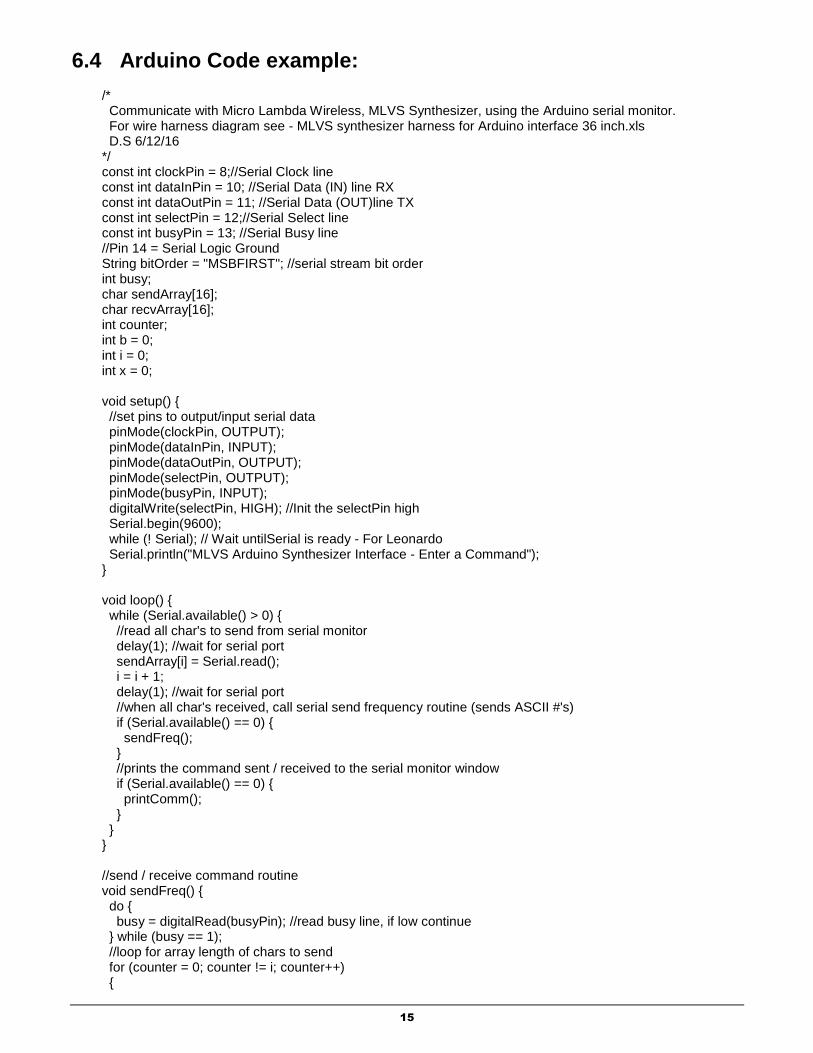
6.4 Arduino Code example: /* Communicate with Micro Lambda Wireless, MLVS Synthesizer, using the Arduino serial monitor. For wire harness diagram see - MLVS synthesizer harness for Arduino interface 36 inch.xls D.S 6/12/16 */ const int clockPin = 8;//Serial Clock line const int dataInPin = 10; //Serial Data (IN) line RX const int dataOutPin = 11; //Serial Data (OUT)line TX const int selectPin = 12;//Serial Select line const int busyPin = 13; //Serial Busy line //Pin 14 = Serial Logic Ground String bitOrder = "MSBFIRST"; //serial stream bit order int busy; char sendArray[16]; char recvArray[16]; int counter; int b = 0; int i = 0; int x = 0; void setup() { //set pins to output/input serial data pinMode(clockPin, OUTPUT); pinMode(dataInPin, INPUT); pinMode(dataOutPin, OUTPUT); pinMode(selectPin, OUTPUT); pinMode(busyPin, INPUT); digitalWrite(selectPin, HIGH); //Init the selectPin high Serial.begin(9600); while (! Serial); // Wait untilSerial is ready - For Leonardo Serial.println("MLVS Arduino Synthesizer Interface - Enter a Command"); } void loop() { while (Serial.available() > 0) { //read all char's to send from serial monitor delay(1); //wait for serial port sendArray[i] = Serial.read(); i = i + 1; delay(1); //wait for serial port //when all char's received, call serial send frequency routine (sends ASCII #'s) if (Serial.available() == 0) { sendFreq(); } //prints the command sent / received to the serial monitor window if (Serial.available() == 0) { printComm(); } } } //send / receive command routine void sendFreq() { do { busy = digitalRead(busyPin); //read busy line, if low continue } while (busy == 1); //loop for array length of chars to send for (counter = 0; counter != i; counter++) {

16
digitalWrite(selectPin, LOW); //selectPin Low and hold low for as long as you are transmitting delayMicroseconds(10); //shift out 8 bits with xx uS delay (Bit Bang) for (b = 0; b < 8; b++) { if (bitOrder == LSBFIRST) { digitalWrite(dataOutPin, !!(sendArray[counter] & (1 << b))); delayMicroseconds(2); } else { digitalWrite(dataOutPin, !!(sendArray[counter] & (1 << (7 - b)))); delayMicroseconds(2); } //toggle clock line digitalWrite(clockPin, HIGH); delayMicroseconds(2); digitalWrite(clockPin, LOW); delayMicroseconds(2); } delayMicroseconds(5); //delay between chars for byte visibility on Dig. scope } digitalWrite(selectPin, HIGH); //pull the selectPin to save the data digitalWrite(dataOutPin, LOW); //set data out low when done digitalWrite(clockPin, LOW); //set clock low when done delayMicroseconds(10); //wait for a xuS between write/read //read back data from unit if available do { busy = digitalRead(busyPin); //read busy line, if low continue } while (busy == 1); digitalWrite(clockPin, HIGH); //clock line high to start for read //read back data from unit if available, 16 bytes for (counter = 0; counter < 16; counter++) { digitalWrite(selectPin, LOW); //selectPin Low and hold low for as long as you are receiving delayMicroseconds(10); //shift in 8 bits with xx uS delay (Bit Bang) for (b = 0; b < 8; b++) { if (bitOrder == LSBFIRST) { recvArray[counter] |= digitalRead(dataInPin) << b; //shift in bits delayMicroseconds(2); } else { recvArray[counter] |= digitalRead(dataInPin) << (7 - b); //shift in bits MSB first delayMicroseconds(2); } //toggle clock line digitalWrite(clockPin, LOW); delayMicroseconds(2); digitalWrite(clockPin, HIGH); delayMicroseconds(2); } delayMicroseconds(5); //delay between chars for byte visibility on Dig. scope } digitalWrite(selectPin, HIGH); //pull the selectPin to save the data digitalWrite(dataOutPin, LOW); //set data out low when done digitalWrite(clockPin, LOW); //set clock low when done delayMicroseconds(10); //wait for a 5uS between commands

17
} //format and print command sent/received to serial monitor window void printComm() { Serial.print("Command Sent = "); for (x = 0; x < 16; x++) { Serial.print(sendArray[x]); } Serial.println(); Serial.print("Info Received = "); for (x = 0; x < 16; x++) { Serial.print(recvArray[x]); } Serial.println(); //clear var. i = 0; x = 0; b = 0; memset(&sendArray[0], 0, sizeof(sendArray)); //clear array memset(&recvArray[0], 0, sizeof(recvArray)); //clear array }

18
7.0 Communication Syntax The following table describes the commands that the MLVS supports. This is a custom syntax created by Micro Lambda Wireless, Inc. All commands are sent and received in ASCII format. The commands are NOT case sensitive. These commands can be used with all forms of communication (USB and Serial). For the following information, please reference Table 1: Serial Hardware Interface Lines, regarding Busy and Data out. MLWI ASCII Command Example: Recommended send data sequence: The format is one select per command string. The string length is variable up to 16 ASCII characters. A decimal point is required for resolution less than 1.0 MHz. The unit will accept a frequency command with a resolution of 0.001 Hz, and it will try to get as close to the frequency requested as possible. So, the command to set the frequency F8000.1 would be sent as follows: Set select low, clock out 01000110 00111000 00110000 00110000 00110000 00101110 00110001 (Ignore spaces, only used to single out each ASCII char), then set select high. The unit should go to 8000.1 MHz. When select goes high, this tells the unit that the user is done and to start interpreting the command. If the command is not understood, the unit will do nothing. Recommended read data sequence: The returned data is variable in length, however, it is recommended that the full 16 bytes of data be read to clear the buffer. Set select low, send the desired read command and set select high. The unit interprets the command and places the requested data in its buffer. Check Busy, then set select low and clock out 16 ASCII nulls while clocking in the data, then set select high. Example: To read the units internal temperature, set select low and send ASCII T (01010100), set select high. Set select low and send 16 00000000 while reading the data line and clocking in bits. Set select high. The information should be similar to +25.0C, in ASCII. All of the memory locations in the unit can be read in this manner, using the R command. In addition to the lines above, there are two, unit status lines: RF LOCK status (J1- Pin 13), and REF LOCK status (J1-Pin 6) which are static lines. These TTL output lines (High = Locked) indicate the overall health of the unit – specifically, that all of the internal phase locked loops are locked. Please note: if there is no 10 MHz Ext. Reference signal applied to J5, the Ref. Lock line will be low indicating an unlock condition and the unit will automatically switch to Internal Ref. mode. The MLVS serial interface lines operate on internal 3.3V logic of a microcontroller; this should allow the unit to communicate in systems operating with 2.5V, 3.3V and 5.0V serial control lines. Maximum voltage on the control lines is -0.5Vdc to +5.5Vdc.

19
7.1 Micro Lambda Wireless Native Commands and Memory Map. Command Function Comments
? Report Status (returns 11000011 in ASCII) D0 = Ref. lock, D1 = RF Lock, D6 = self test, D7 = NOVO lock
F Frequency (ASCII) (Dec. #) ASCII freq in MHz: xxxxx.xxxxxx; (example: F12345.678901234)
MR Recall a user saved frequency setting from memory location (MR25)
0-99, stored @ NOVO location 200-299
MS Save current frequency setting of unit to memory location (MS75) 0-99, stored @ NOVO location 200-299
POWERON Turns ON internal supplies related to +12V input Turns ON supplies.
POWEROFF Turns OFF internal supplies related to +12V input (Low power state)
Microcontroller Supply is always on
SP Synthesizer preset to factory settings. Power cycle required after command
SR Soft Reset Reset CPU, clear var. run CPU code from start; (example: SR)
ST Self-Test Read status byte D2; 1 = Pass; (example: SR, then read data)
T Read internal temp. Returns ASCII chars, reading in Deg. C; (example: T, +35.45C)
V1 Read MLVS internal 1.8V power supply Returns 1.8V
V2 Read MLVS internal 3.3V power supply Returns 3.3V
V3 Read MLVS internal 5.0V power supply Returns 5.0V
V4 Read MLVS internal 11V power supply Returns 11.6V
V5 Read MLVS internal 30V power supply Returns 29.6V
V6 Read MLVS internal -5.0V power supply Returns -5.1V
V7 Read MLVS internal 10V reference voltage Returns 10.0V
R0 Model Number MLVS-0520DS
R1 Serial Number 1234
R2 Xtal Serial Number 0940-002
R3 Fmin, in MHz 50.0
R4 Fmax, in MHz 21000.0
R6 RF min, in dBm 15.0
R7 RF max, in dBm 20.0
R8 Temp min, in Deg. C 0
R9 Temp max, in Deg. C 60
R10 Highest Temp reached, in Deg. C +35.7C
R11 NOVO State - Locked/Unlocked Locked
R12 Firmware Version & date 0001 2017 10 17 10 (Ver., Year, Mo., Day, Hour.)
R13 Unit Health Status – “Good” or Self-test failure information Good or Fail V5 as example
R14 Unit Calibration Status - Yes/No Yes
R15 Self-Test Results - Pass/Fail Pass
R16 Current Output Frequency setting - MHz 2500.123456789
R17 Internal Xtal Setting – Int currently, 1 mode; Internal Xtal
R18 OCXO cal # (Hex), (SCPI) DIAG:CAL:REF:DAC XXXX 0000-FFFF - CPU will set OCXO DAC to this number on start-up
R19 List mode, last index # of current list of frequencies 1000 Decimal = 1000 list frequencies in memory.
R28 Xtal Cal status; Yes / No Yes
R31 Customer part number, if shown on P.O. 123-45-6789 (Shown on unit label as PN:)
R33 Spurious Spec., in dBc -60
R34 Harmonics Spec., in dBc -12
R35 Phase Noise Spec. @ 100 Hz Offset, in dBc/Hz -84
R36 Phase Noise Spec. @ 1 kHz Offset, in dBc/Hz -113
R37 Phase Noise Spec. @ 10 kHz Offset, in dBc/Hz -119
R38 Phase Noise Spec. @ 100 kHz Offset, in dBc/Hz -119
R39 Phase Noise Spec. @ 1 MHz Offset, in dBc/Hz -118
R40 Switching Speed Spec., Opt. S = 50uS or Opt. R = 150uS 50
R41 +12V Supply current Max, in mA 1250
R51 Level flatness spec. in +/- dB (+/- 2.5 = 5.0 total) 2.5
R52 Current Reference Source Setting (Int/Ext). Ext
R55 Installed Options: A, B, C, D, R, and S
R57 USB Com port carriage return send ON/OFF (unit returns CR with Query)
OFF
R58 MLWI Sales (Job) number 10*0024
R59 MLWI Product Outline Drawing # and Revision 99-0101-001 A
R60 Power State (Power supplies on or off) On power-up will default to ON!
"ON" or "OFF"(Low power) - Show status of "poweron" and "poweroff" commands
R200-299 User Save / Recall Frequency setting locations (100 Total) Frequency stored in MHz (ASCII), save and recall using MS & MR commands
R300 User defined default 1 - Frequency setting
R301 User defined default 1 - Mode Settings
R302 User defined default 2 - Frequency setting
R303 User defined default 2 - Mode Settings

20
7.2 SCPI and Binary Commands Power
Description SCPI Cmd. Binary Cmd.
SCPI Param.
Binary Param.
Binary data bytes
Command / Results Examples
RF Module power control (*) OUTP:STAT 0F OFF/ON 0/1 OUTP:STAT ON
Get RF Module power state OUTP:STAT? 0/1 0/1 OUTP:STAT? / OUTP:STAT 1
(*) This command takes about 1500mS
Reset Description SCPI Cmd. Binary Cmd. Result
Reset Frequency *RST (*) 0E 10GHz , Int. Ref. Source , triggering disabled
(*) SPI Interface delay – 300uS, USB Comport delay – 100mS
Frequency
Description SCPI Cmd.
Binary Cmd.
SCPI Param. Binary param.
Binary data bytes
Command / Results Examples
Set Frequency (*) FREQ 0C GHz, MHz, kHz, Hz, mlHz mlHz 6 FREQ 1.2GHz
(*) Each frequency command has a delay according to the specification of the system which can be 50uS (0520DS) to 150uS (0520DR).
Binary Example: Set Output Frequency to 12.123456789123GHz 1. Convert to mlHz 12123456789123 2. Convert to 6 bytes Hex format 0B06B655DA83 3. Append & Send Command 0C0B06B655DA83
Binary Example: Get Output Frequency 12123456789123mlHz 1. Send command: 04 2. Use the received last 6 bytes: 0B06B655DA83 3. Convert from hex to decimal 12123456789123mlHz
Configuration
Description SCPI Cmd. Binary Cmd.
SCPI Param.
Binary Param.
Binary data
bytes Command / Results Examples
Set Ref. Source ROSC:SOUR 06 INT/EXT 0/1 1 ROSC:SOUR EXT
Get Ref. Source ROSC:SOUR? 07 INT/EXT 0/1 1 EXT
Set Internal Ref DAC Value DIAG:CAL:REF:DAC 1B
0 TO 65535
0 TO FFFF
2 DIAG:CAL:REF:DAC 3000
Get Internal Ref DAC Value DIAG:CAL:REF:DAC? none none none none 3000
(*) Response to each command is dependent of the process time and can take 10uS to 1000uS
Diagnostic • SPI diagnostic commands need to be sent twice, the 1st SPI return byte is always Don’t Care
• Binary ASCII return always twice bytes of the HEX return
• If commands format is ASCII, the return is in ASCII, if commands format is HEX, the return is in Hex
• Return value of frequency in mlHz
Description SCPI Cmd.
Binary Cmd.
Binary Return Data bytes
SCPI Return Example Binary Return Example (*)
Get ID- 1.Module# 2.Options 3.Soft. Ver. 4. Serial#
*IDN? 01 11
0520 DS
0001 0002
Get Status BIT0-not used BIT1-RF Locked BIT2-REF Locked BIT3-RF Output BIT4-Voltage status BIT5-not used BIT6-Sweep status BIT7-Comport Status
STAT? 02 01
BIT0 -not used BIT1 -0 Locked, 1 unlocked BIT2 -0 Locked, 1 unlocked BIT3 -0 OFF, 1 ON BIT4 -0 OK, 1 Err BIT5 - not used BIT6 -0 OFF, 1 Run BIT7 -0 Ready, 1 Busy
Get Frequency FREQ? 04 06 12123456789123 0B06B655DA83
Get Ref. Source ROSC:SOUR? 07 01 INT or EXT 00 or 01
Get Temp. (C) DIAG:MEAS? 10 01 38.9 2E
List Points get Size LIST:PVEC:SIZE? N/A N/A LIST:PVEC:SIZE? N/A
List Point get Freq. LIST:PVEC: GET? N/A N/A LIST:PVEC:GET? 15 N/A
(*) In binary mode, first receive byte is always Don’t Care

21
Save / Erase
Description SCPI Cmd. Binary Cmd.
SCPI Param.
Binary Param.
Binary data bytes
Command Example
Save current state in Flash *SAV 26 User Setting 1,2 (**)
1 *SAV 2
Restore current state from Flash *RCL 27 *RCL 2 or *RCL 0 (***)
Save List Table to Flash (*4) LIST:SAV (*5) 4B
none
none
Copy List from Flash to RAM on Request LIST:COPY:REQ 4C none
Automatically Copy List from Flash to RAM upon power up
LIST:COPY:AUTO none LIST:COPY:AUTO:YES/NO
Erase the entire List Table in RAM (*6) LIST:ERAS 22 LIST:ERAS
Erase the entire List Table in FLASH, RAM and NOVO (*)
LIST:ERAS FLASH 23 LIST:ERAS FLASH
(*) “Secure Erase” command (takes about 3 sec and before sending the next command):
• Stops any Sweep
• Resets to 10GHz
• Erase ongoing setting data from NOVO such as last frequency and list point length (**) User Setting includes: Frequency and current Ref. Source selected (***) *RCL 0 is factory default (*4) A delay of at least 100uS per list point is required before sending the next command (*5) The LIST:SAV command allows the list in RAM to be save in FLASH and it will be automatically copied to the RAM upon powerup (*6) The LIST:ERAS command deletes the list points stored in RAM only and is very fast
Sweep/List Run
Description Command Parameters
Binary data bytes
Command Examples
SCPI Binary SCPI Binary SCPI Binary
Run selected List Point
LIST:PVEC:RUN 14 1 to 32767 (Points) 2
LIST:PVEC:RUN 1
Start List Start Fast Sweep Start Normal Sweep
LIST:STAR(T) SWE:FAST:FREQ:STAR(T) SWE:NORM:FREQ:STAR(T)
21 1 - 32767 times 0 – infinite times
2
LIST:STAR 5 SWE:FAST:FREQ:STAR 15 SWE:NORM:FREQ:STAR 0
210005 210015 210000
Stop List / Sweep LIST:STOP or SWE:STOP 20
none
LIST:STOP or SWE:STOP 20
Send Sweep state request
SWE:BUSY? none
SWE:BUSY? none
Get Sweep state SWE:BUSY:YES/NO none SWE:BUSY:YES none

22
Sweep/List Setup
Description SCPI Cmd. Binary Cmd.
SCPI Param.
Binary Param.
Binary data
bytes
Config. SCPI
Config. Binary
Command Example
List point setup RAM FLASH(*4)
LIST:PVEC (*11) (*12)
4A 13
1. List point # (1 to 32767) 2. Freq (*) 3. 0 (Reserved) 4. List Dwell Time (*3) 5. Pulse Mod- N/A (*7) 6. RF Output-N/A (*8) 7. Save to Flash-N/A (*9)
2 6 2 4
None
LIST:PVEC 1,3GHz,0,1s 4A0001 0B06B655DA83 0000 1A000000
List setup and Run
LIST:SETUP (List Setup & run)
15 1. Config. Parameters
4+2+1 1. Point Dwell time(*3) (*10) 2. Times to run: 1 to 32767 0 – infinite 3. Trigger: (**) [xxxx00xx] 0–SW Full, 1–HW Full, 2–HW Point, 3-SW Point 4. Direction (**) [xxxxxx00] 0–Up, 1–Down, 2–Up & Down 3- Down & Up 5. Run Option:(only SCPI) R – run (Optional) (Run in Binary is by default)
LIST:SETUP 2s,0,2,2,R
Fast Sweep and run (*5)
SWE:FAST:FREQ:SETUP (Fast Sweep Setup)
17 1. Start Freq (*) 2. Stop Freq (*) 3. Number of Points (1 to 32767) 4. 0 (Reserved) 5. Config. Param.
6 6 2 2
4+2+1
SWE:FAST:FREQ:SETUP 2GHz,10GHz,100,0,1s,10,0,0, R
Normal Sweep and Run (*6)
SWE:NORM:FREQ:SETUP (Normal Sweep Setup)
1C 1. Start Freq (*) 2. Stop Freq (*) 3. Step Freq (*) 4. 0 (Reserved) 5. Config. Param.
6 6 6 2
4+2+1
SWE:NORM:FREQ:SETUP 2GHz,8GHz,1G Hz,0,5ms, 200,2,2,R
(*) GHz, MHz, KHz, Hz, mlHz, in Binary all units are in mlHz (**) In Binary mode, Trigger and Direction are 1 byte, Trigger location is in bits [03:02], Direction location is in bits [01:00] (*3) us, ms, s (default us) , in Binary dwell time is in uS .
The shortest Dwell time is according to the specification of the system (50uS to 150uS). (*4) Upon completing List point setup (0x13 or 4A), send LIST:SAV (4B) to save in FLASH, more info in in (*9) (*5) In Fast Sweep (either HW Point or SW Point) mode, to reach the Stop frequency, you must send one extra trigger. In Fast Sweep (either HW Full or SW Full) mode, the firmware will automatically add the extra step. Formula = FSTOP – FSTART / POINTS = Frequency Step Size Example: 10000MHz – 1000MHz / 10 = 900MHz step x10 steps + 1 step to reach 10000MHz (*6) In Normal Sweep mode, to reach the Stop frequency, make sure for evenly division by Step frequency
Trigger Types description: 0–SW Full – each frequency point is triggered by a software timer (Dwell time) 1–HW Full – starts a SW Full Trigger Types by an external trigger 2–HW Point – each frequency point is triggered by an external trigger 3-SW Point – each frequency point is triggered by the start button (new command)
(*7) Pulse Mod - not supported (*8) RF Output - not supported since Switching response On/OFF takes about 1500mS (*9) Save to Flash - not supported since writing time to Flash is too long and not efficient for one list mode.
The list is saved in RAM automatically, when ready send a LIST:SAV command (or 13) to save all the lists in Flash. Make sure the list pointer points on the last list to be save in Flash.
(*10) If Point Dwell time > 0, it overwrites the List Dwell Time of each Frequency in the CSV file (*11) Set Ext. or Int. Ref. before sending the ‘LIST:PVEC’ parameters , the reference is kept in the memory for each list point (*12) The MLVS updates the list and number of frequencies in RAM (only) after each LIST:PVEC command.
As long as you make the list sequentially, the old list will be erased automatically and the erase command is not needed. Example: If you have saved 20 frequencies using the LIST:PVEC 1…, to LIST:PVEC 20… commands, the unit knows that you have 20 frequencies in the list, start from 1 to 20 If you then, without turning off the power, save 5 frequencies in RAM using LIST:PVEC 1…, to LIST:PVEC 5… your list is now 5 frequencies long, and list points 6-20 are no longer accessible (virtually erased).

23
Example: Fast Frequency Sweep Setup and Run command: Start Frequency: 5 GHz, Stop Frequency: 8 GHz Number of Points Between Frequencies (inclusive): 30 Dwell Time: 3 sec, Number of times to run sweep: 2 Enable Sweep Trigger: Yes, Enable Sweep Point Triggers: No, Direction: Up
Field Start Freq. Stop Freq. No. Points Reserved Dwell Time No. Runs Trigger Direction
Units milliHertz milliHertz μs Bool
Decimal 5000000000000 8000000000000 30 0 3000000 2 Yes Up
Binary 048C27395000 0746A5288000 001E 0000 002DC6C0 0002 4 4
17 04 8C 27 39 50 00 07 46 A5 28 80 00 00 1E 00 00 00 2D C6 C0 00 02 04 After this command is executed, ONE Sweep trigger signal should be applied. Example: Normal Frequency Sweep Setup with Software-Point trigger: Send Normal Sweep setup: 1C 00448CE31B30 13196AE931C2 000025AA0760 0000 00000064 0000 0C Send Start Normal Sweep to set the 1st Frequency: 21 Continue sending 21 commands for each next Frequency Point

24
8.0 Hardware Installation Information The unit may be installed into a system using four #4-40 screws, through the mounting surface, on the sides, two on each side. Alternately, four #4-40 screws can be attached from the bottom side through the mounting surface, in the four mounting holes. The mounting hole dimensions and Molex connector (J1), and mating connector information and are shown in the drawing number 99-0101-001 in this document. The USB connector (J2) is a standard Mini-B. The DC power supply connector (J3) is a barrel plug with a center pin diameter of 1.3mm and outer connection point diameter of 3.6mm. The center pin is the positive contact. Recommended AC/DC (12Vdc, 46W) wall mount adapter is Digi-Key part number 1647-1009-ND
9.0 Technical Support For Technical support please contact: Micro Lambda Wireless, Inc. 46515 Landing Pkwy. Fremont, CA 94538 Ph: (510) 770-9221 Fax: (510) 770-9213 Email: [email protected] You can visit our website at http://www.microlambdawireless.com for updated information, specifications and downloads.
10.0 Warranty Seller warrants for a period of twelve (12) months from the date of original shipment that the products will be free from defects in material and workmanship and design (if of Micro Lambda Wireless, Inc. design) and will be in conformity with applicable specifications and drawings and all other contractual requirements. However, this warranty shall not apply to any product which that has been subjected to misuse, misapplication, accident, improper installation, neglect, unauthorized repair, alteration, adjustment, inundation or fire. See the complete warranty and return policy document number 96-0200-005 Rev A at our website at http://www.microlambdawireless.com.