ml2281, ml2282 *, ml2284 #, ml2288 # serial i/o 8...
TRANSCRIPT
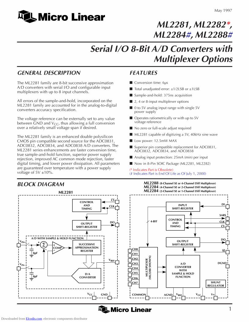
BLOCK DIAGRAM
1
May 1997
ML2281, ML2282*,ML2284#, ML2288#
Serial I/O 8-Bit A/D Converters withMultiplexer Options
GENERAL DESCRIPTION
The ML2281 family are 8-bit successive approximationA/D converters with serial I/O and configurable inputmultiplexers with up to 8 input channels.
All errors of the sample-and-hold, incorporated on theML2281 family are accounted for in the analog-to-digitalconverters accuracy specification.
The voltage reference can be externally set to any valuebetween GND and VCC, thus allowing a full conversionover a relatively small voltage span if desired.
The ML2281 family is an enhanced double polysiliconCMOS pin compatible second source for the ADC0831,ADC0832, ADC0834, and ADC0838 A/D converters. TheML2281 series enhancements are faster conversion time,true sample-and-hold function, superior power supplyrejection, improved AC common mode rejection, fasterdigital timing, and lower power dissipation. All parametersare guaranteed over temperature with a power supplyvoltage of 5V ±10%.
FEATURES
Conversion time: 6µs
Total unadjusted error: ±1/2LSB or ±1LSB
Sample-and-hold: 375ns acquisition
2, 4 or 8-input multiplexer options
0 to 5V analog input range with single 5Vpower supply
Operates ratiometrically or with up to 5Vvoltage reference
No zero or full-scale adjust required
ML2281 capable of digitizing a 5V, 40kHz sine wave
Low power: 12.5mW MAX
Superior pin compatible replacement for ADC0831,ADC0832, ADC0834, and ADC0838
Analog input protection: 25mA (min) per input
Now in 8-Pin SOIC Package (ML2281, ML2282)
INPUTSHIFT-REGISTER
OUTPUTSHIFT-REGISTER
SHUNTREGULATOR
CONTROLAND
TIMING
DI
SARS
CLK
CS
DO
4-BIT
SE
DGND
V+VCCVREFAGNDCOMMON
CH7
CH6
CH5
CH4
CH3
CH2
CH1
CH0
A/DCONVERTER
WITHSAMPLE & HOLD
FUNCTIONMU
LTIP
LEX
ER(M
L228
8 SH
OW
N)
Σ
VREF
CLK
CS
VIN–
SUCCESSIVEAPPROXIMATION
REGISTER
D/ACONVERTER
+
–
OUTPUTSHIFT-REGISTER
CONTROLAND
TIMING
COMP
A/D WITH SAMPLE & HOLD FUNCTION
8pF
8pF
–
+VIN+
VCC GND
DO
ML2281
ML2288 (8-Channel SE or 4-Channel Diff Multiplexer)ML2284 (4-Channel SE or 2-Channel Diff Multiplexer)ML2284 (2-Channel SE or 1-Channel Diff Multiplexer)
(* Indicates Part is Obsolete)(# Indicates Part is End Of Life as Of July 1, 2000)
Downloaded from Elcodis.com electronic components distributor
ML2281, ML2282, ML2284, ML2288
2
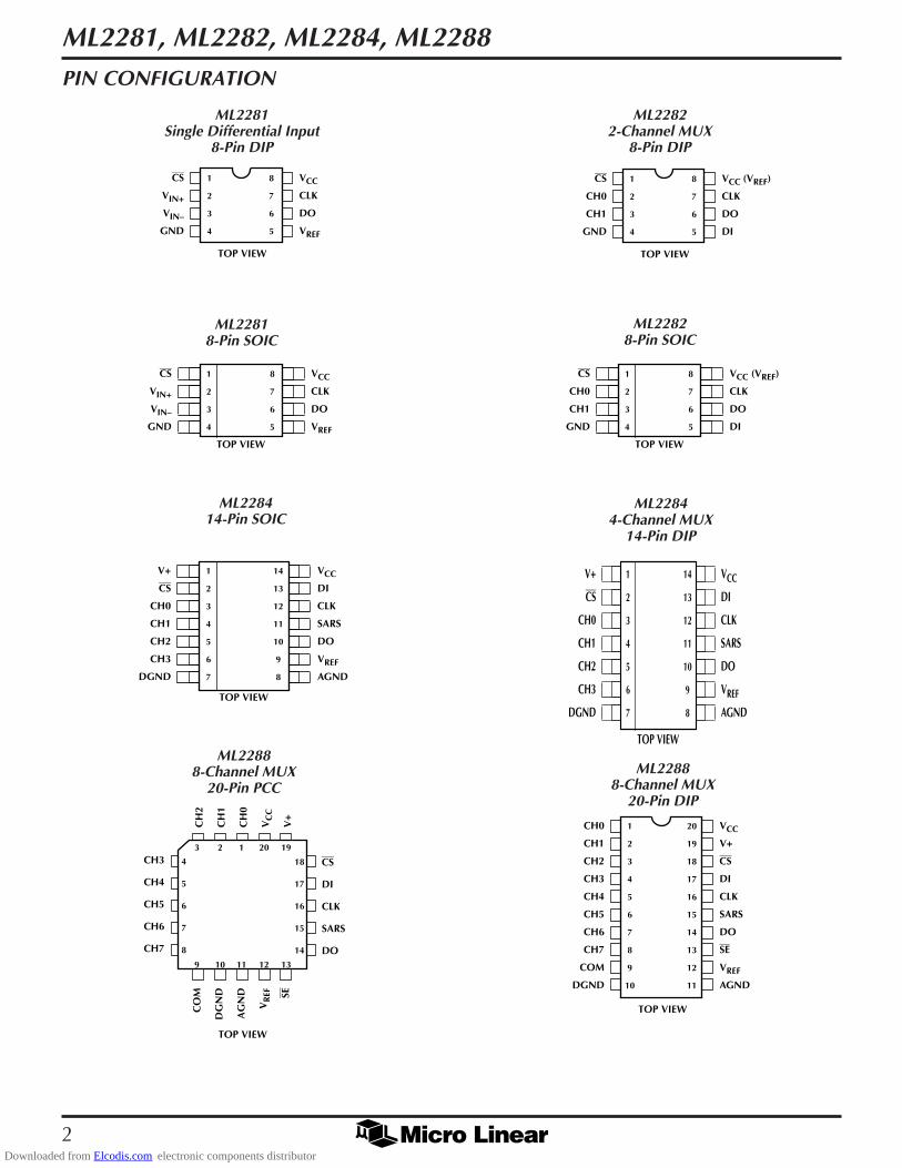
PIN CONFIGURATION
CS
VIN+
VIN–
GND
VCC
CLK
DO
VREF
1
2
3
4
8
7
6
5
TOP VIEW
TOP VIEW
CS
VIN+
VIN–
GND
VCC
CLK
DO
VREF
1
2
3
4
8
7
6
5
TOP VIEW
CS
CH0
CH1
GND
VCC (VREF)
CLK
DO
DI
1
2
3
4
8
7
6
5
TOP VIEW
V+
CS
CH0
CH1
CH2
CH3
DGND
VCC
DI
CLK
SARS
DO
VREF
AGND
1
2
3
4
5
6
7
14
13
12
11
10
9
8
ML2281Single Differential Input
8-Pin DIP
ML22822-Channel MUX
8-Pin DIP
ML22818-Pin SOIC
ML22828-Pin SOIC
ML228414-Pin SOIC
CH0
CH1
CH2
CH3
CH4
CH5
CH6
CH7
COM
DGND
VCC
V+
CS
DI
CLK
SARS
DO
SE
VREF
AGND
1
2
3
4
5
6
7
8
9
10
20
19
18
17
16
15
14
13
12
11
TOP VIEW
ML22888-Channel MUX
20-Pin DIP
CS
DI
CLK
SARS
DO
CH3
CH4
CH5
CH6
CH7
9 10 11 12 13
CH
2
CH
1
CH
0
VC
C
V+
CO
M
DG
ND
AG
ND
VR
EF SE
4
5
6
7
8
3 2 1 20 19
18
17
16
15
14
TOP VIEW
TOP VIEW
V+
CS
CH0
CH1
CH2
CH3
DGND
VCC
DI
CLK
SARS
DO
VREF
AGND
1
2
3
4
5
6
7
14
13
12
11
10
9
8
ML22844-Channel MUX
14-Pin DIP
ML22888-Channel MUX
20-Pin PCC
CS
CH0
CH1
GND
VCC (VREF)
CLK
DO
DI
1
2
3
4
8
7
6
5
TOP VIEW
Downloaded from Elcodis.com electronic components distributor
ML2281, ML2282, ML2284, ML2288
3
NAME FUNCTION
VCC Positive supply. 5V ± 10%
DGND Digital ground. 0 volts. All digital inputs andoutputs are referenced to this point.
AGND Analog ground. The negative reference voltagefor A/D converter.
CH0-7, Analog inputs. Digitally selected to be singleVIN+, VIN– ended (VIN) or; VIN+ or VIN– of a differential
input. Analog range = GND - VIN - VCC.
COM Common reference point for analog inputs.A/D conversion is performed on voltagedifference between analog input and thiscommon reference point if single-endconversion is specified.
VREF Reference. The positive reference voltage forA/D converter.
SE Shift enable. Input controls whether LSB firstbit stream is shifted out on serial output DO.If SE = 1, MSB first is shifted out only. If SE = 0,an MSB first bit stream is shifted out, then asecond bit stream with LSB first is shifted outafter end of conversion.
V+ Input to the Shunt Regulator.
PIN DESCRIPTION
NAME FUNCTION
DO Data out. Digital output which contains resultof A/D conversion. The serial data is clockedout on falling edges of CLK.
SARS Successive approximation register status.Digital output which indicates that aconversion is in progress. When SARS goesto 1, the sampling window is closed andconversion begins. When SARS goes to 0,conversion is completed. When CS = 1, SARSis in high impedance state.
CLK Clock. Digital input which clocks data in onDI on rising edges and out on DO on fallingedges. Also used to generate clocks for A/Dconversion.
DI Data input. Digital input which contains serialdata to program the MUX and channelassignments.
CS Chip select. Selects the chip for multiplexerand channel assignment and A/D conversion.When CS = 1, all digital outputs are in highimpedance state. When CS = 0, normal A./Dconversion takes place.
Downloaded from Elcodis.com electronic components distributor
ML2281, ML2282, ML2284, ML2288
4
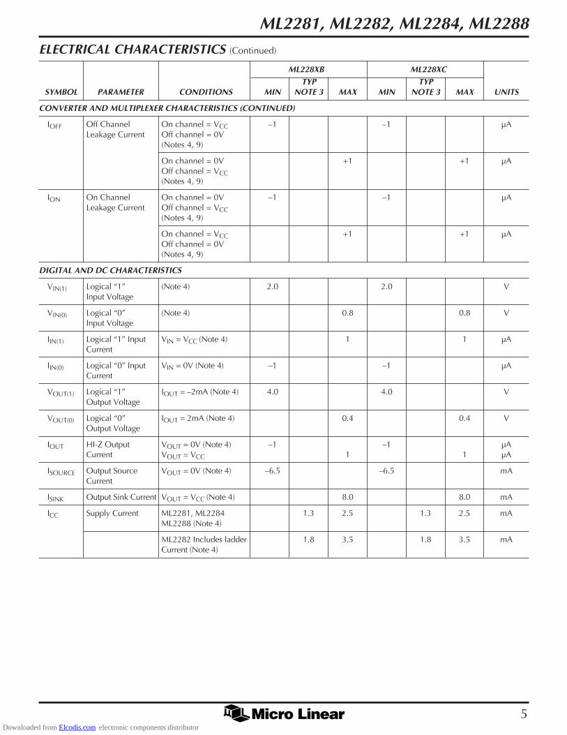
ELECTRICAL CHARACTERISTICSUnless otherwise specified, TA = TMIN to TMAX, VCC = VREF = 5V ±10%, and fCLK = 1.333MHz.
ML228XB ML228XCTYP TYP
SYMBOL PARAMETER CONDITIONS MIN NOTE 3 MAX MIN NOTE 3 MAX UNITS
CONVERTER AND MULTIPLEXER CHARACTERISTICS
Total Unadjusted VREF = VCC (Notes 4, 6) ±1/2 ±1 LSBError
Reference Input (Notes 4, 7) 10 15 20 10 15 20 kWResistance
Common-Mode (Notes 4, 8) GND VCC GND VCC VInput Range –0.05 +0.05 –0.05 +0.05
DC Common-Mode Common mode voltage ±1/16 ±1/4 ±1/16 ±1/4 LSBError voltage GND to VCC/2
(Note 5)
AC Common-Mode Common mode voltage ±1/4 ±1/4 LSBError GND to VCC/2,
0 to 50kHz (Note 5)
DC Power Supply VCC = 5V ±10% ±1/32 ±1/4 ±1/32 ±1/4 LSBSensitivity VREF - VCC +0.1V
(Note 5)
AC Power Supply 100mVP-P, 25kHz sine ±1/4 ±1/4 LSBSensitivity on VCC (Note 5)
Change in Zero 15mA into V+ ±1/2 ±1/2 LSBError from VCC=5V VCC = N.C. VREF = 5Vto Internal Zener (Note 5)Operation
VZ Internal Diode 15mA into V+ 6.9 6.9 VRegulated Break-down (at V+)
V+ Input Resistance (Note 4) 20 35 20 35 kW
ABSOLUTE MAXIMUM RATINGSAbsolute maximum ratings are those values beyond whichthe device could be permanently damaged. Absolutemaximum ratings are stress ratings only and functionaldevice operation is not implied.
Current into V+ ...................................................... 15mASupply Voltage, VCC ................................................. 6.5VVoltage
Logic Inputs ........................................... –7 to VCC +7VAnalog Inputs ................................ –0.3V to VCC +0.3V
Input Current per Pin (Note 1) ..............................±25mAStorage Temperature ................................ –65°C to 150°CPackage Dissipation
at TA = 25°C (Board Mount) .............................800mW
Lead Temperature (Soldering 10 sec.)Dual-In-Line Package (Molded) .......................... 260°CDual-In-Line Package (Ceramic) ......................... 300°CMolded Chip Carrier Package
Vapor Phase (60 sec.) ..................................... 215°CInfrared (15 sec.) ............................................. 220°C
OPERATING CONDITIONS
Supply Voltage, VCC ............................ 4.5VDC to 6.3VDCTemperature Range (Note 2) ................. TMIN - TA - TMAX
ML2281/2/4/8 BIX .................................. –40°C to 85°CML2281/2/4/8 CIXML2281/2/4/8 BCX ....................................0°C to 70°CML2281/2/4/8 CCX
Downloaded from Elcodis.com electronic components distributor
ML2281, ML2282, ML2284, ML2288
5
ELECTRICAL CHARACTERISTICS (Continued)
ML228XB ML228XCTYP TYP
SYMBOL PARAMETER CONDITIONS MIN NOTE 3 MAX MIN NOTE 3 MAX UNITS
CONVERTER AND MULTIPLEXER CHARACTERISTICS (CONTINUED)
IOFF Off Channel On channel = VCC –1 –1 µALeakage Current Off channel = 0V
(Notes 4, 9)
On channel = 0V +1 +1 µAOff channel = VCC(Notes 4, 9)
ION On Channel On channel = 0V –1 –1 µALeakage Current Off channel = VCC
(Notes 4, 9)
On channel = VCC +1 +1 µAOff channel = 0V(Notes 4, 9)
DIGITAL AND DC CHARACTERISTICS
VIN(1) Logical “1” (Note 4) 2.0 2.0 VInput Voltage
VIN(0) Logical “0” (Note 4) 0.8 0.8 VInput Voltage
IIN(1) Logical “1” Input VIN = VCC (Note 4) 1 1 µACurrent
IIN(0) Logical “0” Input VIN = 0V (Note 4) –1 –1 µACurrent
VOUT(1) Logical “1” IOUT = –2mA (Note 4) 4.0 4.0 VOutput Voltage
VOUT(0) Logical “0” IOUT = 2mA (Note 4) 0.4 0.4 VOutput Voltage
IOUT HI-Z Output VOUT = 0V (Note 4) –1 –1 µACurrent VOUT = VCC 1 1 µA
ISOURCE Output Source VOUT = 0V (Note 4) –6.5 –6.5 mACurrent
ISINK Output Sink Current VOUT = VCC (Note 4) 8.0 8.0 mA
ICC Supply Current ML2281, ML2284 1.3 2.5 1.3 2.5 mAML2288 (Note 4)
ML2282 Includes ladder 1.8 3.5 1.8 3.5 mACurrent (Note 4)
Downloaded from Elcodis.com electronic components distributor
ML2281, ML2282, ML2284, ML2288
6
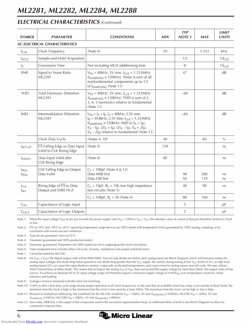
ELECTRICAL CHARACTERISTICS (Continued)
TYP LIMITSYMBOL PARAMETER CONDITIONS MIN NOTE 3 MAX UNITS
AC ELECTRICAL CHARACTERISTICS
fCLK Clock Frequency (Note 4) 10 1.333 kHz
tACQ Sample-and-Hold Acquisition 1/2 1/fCLK
tC Conversion Time Not including MUX adddressing time 8 1/fCLK
SNR Signal to Noise Ratio VIN = 40kHz, 5V sine. fCLK = 1.333MHz 47 dBML2281 (fSAMPLING » 120kHz). Noise is sum of all
nonfundamental components up to 1/2of fSAMPLING (Note 11)
THD Total Harmonic Distortion VIN = 40kHz, 5V sine. fCLK = 1.333MHz –60 dBML2281 (fSAMPLING » 120kHz). THD is sum of 2,
3, 4, 5 harmonics relative to fundamental(Note 11)
IMD Intermodulation Distortion VIN = fA + fB. fA = 40kHz, 2.5V sine. –60 dBML2281 fB = 39.8kHz, 2.5V Sine, fCLK = 1.333MHz
(fSAMPLING » 120kHz). IMD is (fA + fB),(fA – fB), (2fA + fB), (2fA – fB), (fA + 2fB),(fA – 2fB) relative to fundamental (Note 11)
Clock Duty Cycle (Notes 4, 10) 40 60 %
tSET-UP CS Falling Edge or Data Input (Note 4) 130 nsValid to CLK Rising Edge
tHOLD Data Input Valid after (Note 4) 80 nsCLK Rising Edge
tPD1, CLK Falling Edge to Output CL = 100pF (Note 4 & 12)tPD0 Data Valid Data MSB first 90 200 ns
Data LSB first 50 110 ns
t1H, Rising Edge of CS to Data CL = 10pF, RL = 10k (see high impedance 40 90 nst0H Output and SARS Hi-Z test circuits) (Note 5)
CL = 100pF, RL = 2k (Note 4) 80 160 ns
CIN Capacitance of Logic Input 5 pF
COUT Capacitance of Logic Outputs 5 pF
Note 1: When the input voltage (VIN) at any pin exceeds the power supply rails (VIN < GND or VIN > VCC) the absolute value of current at that pin should be limited to 25mAor less.
Note 2: 0°C to 70°C and –40°C to +85°C operating temperature range devices are 100% tested with temperature limits guaranteed by 100% testing, sampling, or bycorrelation with worst-case test conditions.
Note 3: Typicals are parametric norm at 25°C.
Note 4: Parameter guaranteed and 100% production tested.
Note 5: Parameter guaranteed. Parameters not 100% tested are not in outgoing quality level calculation.
Note 6: Total unadjusted error includes offset, full-scale, linearity, multiplexer and sample-and-hold errors.
Note 7: Cannot be tested for ML2282.
Note 8: For VIN– ³ VIN+ the digital output code will be 0000 0000. Two on-chip diodes are tied to each analog input (see Block Diagram) which will forward conduct foranalog input voltages one diode drop below ground or one diode drop greater than the VCC supply. Be careful, during testing at low VCC levels (4.5V), as high levelanalog inputs (5V) can cause this input diode to conduct—especially at elevated temperatures, and cause errors for analog inputs near full-scale. The spec allows50mV forward bias of either diode. This means that as long as the analog VIN or VREF does not exceed the supply voltage by more than 50mV, the output code will becorrect. To achieve an absolute 0V to 5V input voltage range will therefore require a minimum supply voltage of 4.950VDC over temperature variations, initialtolerance and loading.
Note 9: Leakage current is measured with the clock not switching.
Note 10: A 40% to 60% clock duty cycle range insures proper operation at all clock frequencies. In the case that an available clock has a duty cycle outside of these limits, theminimum time the clock is high or the minimum time the clock is low must be at least 300ns. The maximum time the clock can be high or low is 60µs.
Note 11: Because of multiplexer addressing, test conditions for the ML2282 would be VIN = 34kHz, 5V sine (fSAMPLING » 102kHz); ML2284 VIN = 32kHz, 5V sine(fSAMPLING » 95kHz); ML2288 VIN = 30kHz, 5V sine (fSAMPLING » 89kHz).
Note 12: Since data, MSB first, is the output of the comparator used in the successive approximation loop, an additional delay is built in (see Block Diagram) to allow forcomparator response time.
Downloaded from Elcodis.com electronic components distributor
ML2281, ML2282, ML2284, ML2288
7
VCC
DATAOUTPUT
CL
CLRL
DATAOUTPUT
t1H
t0H
t1H
t0H
CS
VCC
GND
VOH
GND
50%10%
90%
t1H
90%DO ANDSARS OUTPUTS
CS
DO ANDSARS OUTPUTS
GND
VCC
VCC
VOL 10%
t0H
50%10%
90%
tr
tr
RL
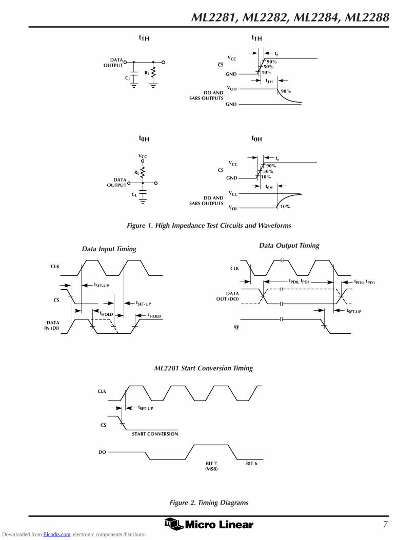
Figure 1. High Impedance Test Circuits and Waveforms
CLK
CLK
CS
DO
tSET-UPtPD0, tPD1
tSET-UP
tSET-UPtHOLD
tHOLD
CS
DATAIN (DI)
CLK
DATAOUT (DO)
SE
tSET-UP
START CONVERSION
BIT 7(MSB)
BIT 6
tPD0, tPD1
Figure 2. Timing Diagrams
Data Input Timing Data Output Timing
ML2281 Start Conversion Timing
Downloaded from Elcodis.com electronic components distributor
ML2281, ML2282, ML2284, ML2288
8
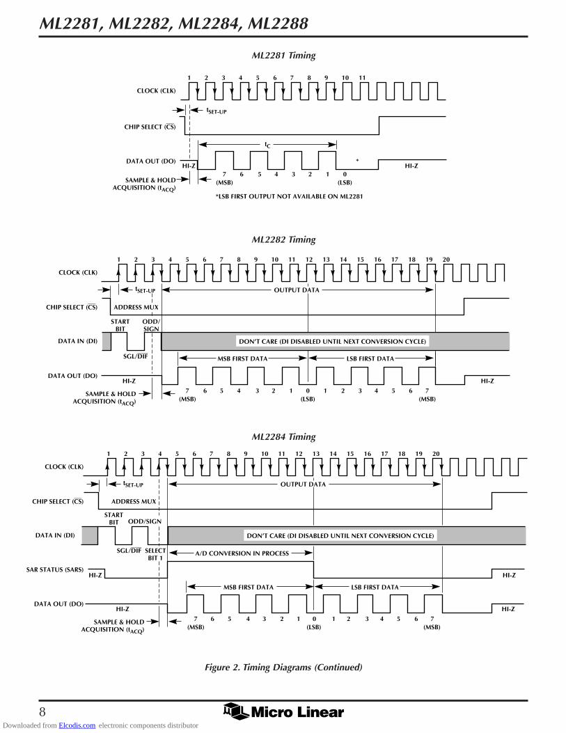
CLOCK (CLK)
CHIP SELECT (CS)
DATA OUT (DO)
CLOCK (CLK)
CHIP SELECT (CS)
DATA IN (DI)
DATA OUT (DO)
HI-Z
ADDRESS MUX
OUTPUT DATA
LSB FIRST DATAMSB FIRST DATA
STARTBIT
SGL/DIF
ODD/SIGN
*LSB FIRST OUTPUT NOT AVAILABLE ON ML2281
HI-Z
HI-Z HI-Z
SAMPLE & HOLDACQUISITION (tACQ)
SAMPLE & HOLDACQUISITION (tACQ)
1
7 6 5 4 3 2 1 0
*
(MSB)
7 6 5 4 3 2 1 1 2 3 4 5 6(MSB)
7(MSB)
0(LSB)
(LSB)
2 3 4 5 6 7 8 9 10 11
1 2 3 4 5 6 7 8 9 10 11 12 13 14 15 16 17 18 19 20
tC
tSET-UP
tSET-UP
DON’T CARE (DI DISABLED UNTIL NEXT CONVERSION CYCLE)
CLOCK (CLK)
CHIP SELECT (CS)
DATA IN (DI)
DATA OUT (DO)
SAR STATUS (SARS)
ADDRESS MUX
OUTPUT DATA
LSB FIRST DATAMSB FIRST DATA
STARTBIT
SGL/DIF SELECTBIT 1
ODD/SIGN
HI-Z HI-Z
HI-Z HI-Z
SAMPLE & HOLDACQUISITION (tACQ)
7 6 5 4 3 2 0 1 2 3 4 5(MSB)
6 7(MSB)
1(LSB)
1 2 3 4 5 6 7 8 9 10 11 12 13 14 15 16 17 18 19 20
A/D CONVERSION IN PROCESS
tSET-UP
DON’T CARE (DI DISABLED UNTIL NEXT CONVERSION CYCLE)
ML2281 Timing
ML2282 Timing
ML2284 Timing
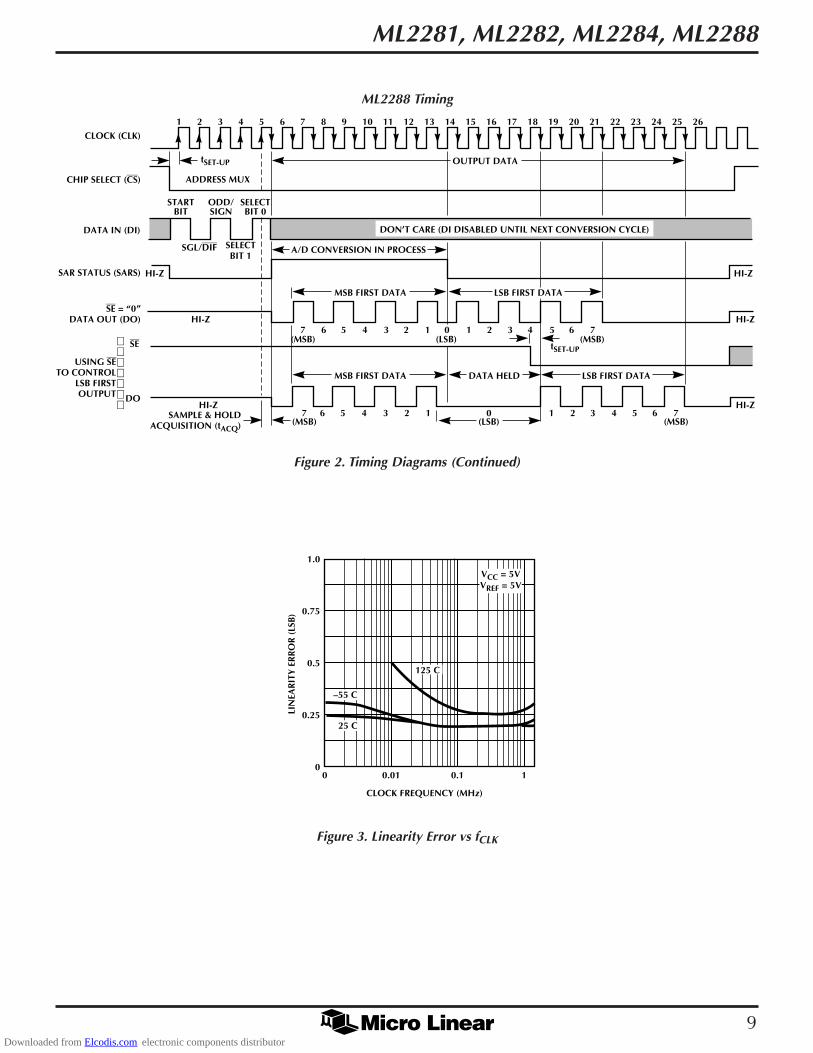
Figure 2. Timing Diagrams (Continued)
Downloaded from Elcodis.com electronic components distributor
ML2281, ML2282, ML2284, ML2288
9
CLOCK (CLK)
CHIP SELECT (CS)
DATA IN (DI)
DO
USING SETO CONTROL
LSB FIRSTOUTPUT
SAR STATUS (SARS)
SE = “0”DATA OUT (DO)
ADDRESS MUX
OUTPUT DATA
LSB FIRST DATAMSB FIRST DATA
STARTBIT
SGL/DIF SELECTBIT 1
ODD/SIGN
SELECTBIT 0
HI-Z HI-Z
HI-ZHI-Z
HI-ZHI-Z
SAMPLE & HOLDACQUISITION (tACQ)
7 6 5 4 3 2 0 1 2 3 4 5(MSB)
6 7(MSB)
1(LSB)
1 2 3 4 5 6 7 8 9 10 11 12 13 14 15 16 17 18 19 20 21 22 23 24 25 26
A/D CONVERSION IN PROCESS
DATA HELD LSB FIRST DATAMSB FIRST DATA
(LSB) (MSB)(MSB)7 6 5 4 3 2 1 0 1 2 3 4 5 6 7
tSET-UP
tSET-UP
DON’T CARE (DI DISABLED UNTIL NEXT CONVERSION CYCLE)
SE
ML2288 Timing
Figure 2. Timing Diagrams (Continued)
1.0
0.75
0.5
0.25
0
LIN
EAR
ITY
ER
RO
R (
LSB
)
CLOCK FREQUENCY (MHz)
0 0.01 0.1 1
VCC = 5VVREF = 5V
125 C
–55 C
25 C
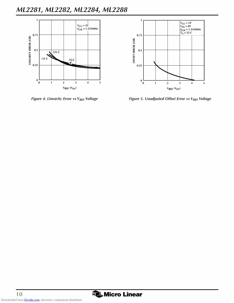
Figure 3. Linearity Error vs fCLK
Downloaded from Elcodis.com electronic components distributor
ML2281, ML2282, ML2284, ML2288
10
1
0.75
0.5
0.25
0
LIN
EAR
ITY
ER
RO
R (
LSB
)
VREF (VDC)
0 2 3 541
VCC = 5VfCLK = 1.333MHz
125 C
–55 C 25 C
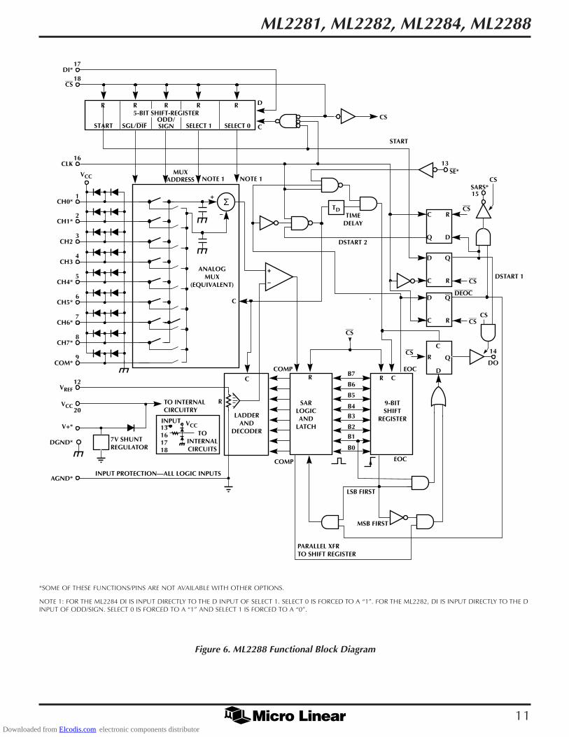
Figure 4. Linearity Error vs VREF Voltage
1
0.75
0.5
0.25
0
OFF
SET
ERR
OR
(LS
B)
VREF (VDC)
0 2 3 541
VCC = 5VVIN = 0VfCLK = 1.333MHzTA = 25 C
Figure 5. Unadjusted Offset Error vs VREF Voltage
Downloaded from Elcodis.com electronic components distributor
ML2281, ML2282, ML2284, ML2288
11
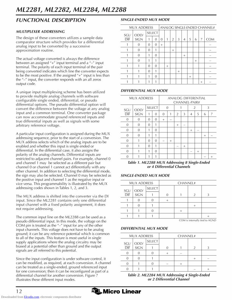
*SOME OF THESE FUNCTIONS/PINS ARE NOT AVAILABLE WITH OTHER OPTIONS.
NOTE 1: FOR THE ML2284 DI IS INPUT DIRECTLY TO THE D INPUT OF SELECT 1. SELECT 0 IS FORCED TO A “1”. FOR THE ML2282, DI IS INPUT DIRECTLY TO THE DINPUT OF ODD/SIGN. SELECT 0 IS FORCED TO A “1” AND SELECT 1 IS FORCED TO A “0”.
Figure 6. ML2288 Functional Block Diagram
C
Q
R
D
R
D
C
Q
D
C
Q
R
D
C
Q
R
+
–
–
+
ANALOGMUX
(EQUIVALENT)
Σ1
CH0*
16CLK
17DI*
18CS
CH1*
CH6*
VREF
VCC
V+*
DGND*
AGND*
2
CH23
CH34
CH4*5
CH5*6
7
CH7*8
COM*9
12
20TO INTERNALCIRCUITRY
7V SHUNTREGULATOR
INPUT PROTECTION—ALL LOGIC INPUTS
C
C
R
LADDERAND
DECODER
SARLOGICAND
LATCH
9-BITSHIFT
REGISTER
COMPB7
B6
B5
B4
14
DO
B2
B3
B1
B0
CS
CS
CS
COMP
PARALLEL XFRTO SHIFT REGISTER
MSB FIRST
LSB FIRST
EOC
EOCRR C
CS
DEOC
CS
SE*
CS
CS
CS
TD
VCC
VCC
TOINTERNALCIRCUITS
INPUT13161718
MUXADDRESS NOTE 1
13
SARS*15
NOTE 1
SELECT 0SELECT 1START
R R R R R D
CSGL/DIF
5-BIT SHIFT-REGISTERODD/SIGN
TIMEDELAY
DSTART 2
START
DSTART 1
Downloaded from Elcodis.com electronic components distributor
ML2281, ML2282, ML2284, ML2288
12
FUNCTIONAL DESCRIPTION
MULTIPLEXER ADDRESSING
The design of these converters utilizes a sample datacomparator structure which provides for a differentialanalog input to be converted by a successiveapproximation routine.
The actual voltage converted is always the differencebetween an assigned “+” input terminal and a “–” inputterminal. The polarity of each input terminal of the pairbeing converted indicates which line the converter expectsto be the most positive. If the assigned “+” input is less thanthe “–” input, the converter responds with an all zerosoutput code.
A unique input multiplexing scheme has been utilizedto provide multiple analog channels with softwareconfigurable single ended, differential, or pseudodifferential options. The pseudo differential option willconvert the difference between the voltage at any analoginput and a common terminal. One converter packagecan now accommodate ground referenced inputs andtrue differential inputs as well as signals with somearbitrary reference voltage.
A particular input configuration is assigned during the MUXaddressing sequence, prior to the start of a conversion. TheMUX address selects which of the analog inputs are to beenabled and whether this input is single ended ordifferential. In the differential case, it also assigns thepolarity of the analog channels. Differential inputs arerestricted to adjacent channel pairs. For example, channel 0and channel 1 may be selected as a different pair butchannel 0 or channel 1 cannot act differentially with anyother channel. In addition to selecting the differential mode,the sign may also be selected. Channel 0 may be selected asthe positive input and channel 1 as the negative input orvice versa. This programmability is illustrated by the MUXaddressing codes shown in Tables 1, 2, and 3.
The MUX address is shifted into the converter via the DIinput. Since the ML2281 contains only one differentialinput channel with a fixed polarity assignment, it doesnot require addressing.
The common input line on the ML2288 can be used as apseudo differential input. In this mode, the voltage on theCOM pin is treated as the “–” input for any of the otherinput channels. This voltage does not have to be analogground; it can be any reference potential which is commonto all of the inputs. This feature is most useful in singlesupply applications where the analog circuitry may bebiased at a potential other than ground and the outputsignals are all referred to this potential.
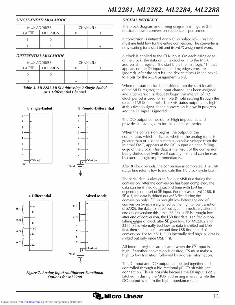
Since the input configuration is under software control, itcan be modified, as required, at each conversion. A channelcan be treated as a single-ended, ground referenced inputfor one conversion; then it can be reconfigured as part of adifferential channel for another conversion. Figure 7illustrates these different input modes.
MUX ADDRESS ANALOG SINGLE-ENDED CHANNEL#
SGL/ ODD/SELECT
DIF SIGN 1 0 0 1 2 3 4 5 6 7 COM
1 0 0 0 + –
1 0 0 1 + –
1 0 1 0 + –
1 0 1 1 + –
1 1 0 0 + –
1 1 0 1 + –
1 1 1 0 + –
1 1 1 1 + –
SINGLE-ENDED MUX MODE
MUX ADDRESS ANALOG DIFFERENTIALCHANNEL-PAIR#
SGL/ ODD/SELECT 0 1 2 3
DIF SIGN 1 0 0 1 2 3 4 5 6 7
0 0 0 0 + –
0 0 0 1 + –
0 0 1 0 + –
0 0 1 1 + –
0 1 0 0 – +
0 1 0 1 – +
0 1 1 0 – +
0 1 1 1 – +
DIFFERENTIAL MUX MODE
Table 1. ML2288 MUX Addressing 8 Single-Endedor 4 Differential Channels
MUX ADDRESS CHANNEL#
SGL/ ODD/SELECT
DIF SIGN 1 0 1 2 3
1 0 0 +
1 0 1 +
1 1 0 +
1 1 1 +
SINGLE-ENDED MUX MODE
MUX ADDRESS CHANNEL#
SGL/ ODD/SELECT
DIF SIGN 1 0 1 2 3
0 0 0 + –
0 0 1 + –
0 1 0 – +
0 1 1 – +
DIFFERENTIAL MUX MODE
COM is internally tied to AGND
Table 2. ML2284 MUX Addressing 4 Single-Endedor 2 Differential Channel
Downloaded from Elcodis.com electronic components distributor
ML2281, ML2282, ML2284, ML2288
13
DIGITAL INTERFACE
The block diagram and timing diagrams in Figures 2-5illustrate how a conversion sequence is performed.
A conversion is initiated when CS is pulsed low. This linemust me held low for the entire conversion. The converter isnow waiting for a start bit and its MUX assignment word.
A clock is applied to the CLK input. On each rising edgeof the clock, the data on DI is clocked into the MUXaddress shift register. The start bit is the first logic “1” thatappears on the DI input (all leading edge zeros areignored). After the start bit, the device clocks in the next 2to 4 bits for the MUX assignment word.
When the start bit has been shifted into the start locationof the MUX register, the input channel has been assignedand a conversion is about to begin. An interval of 1/2clock period is used for sample & hold settling through theselected MUX channels. The SAR status output goes highat this time to signal that a conversion is now in progressand the DI input is ignored.
The DO output comes out of High impedance andprovides a leading zero for this one clock period.
When the conversion begins, the output of thecomparator, which indicates whether the analog input isgreater than or less than each successive voltage from theinternal DAC, appears at the DO output on each fallingedge of the clock. This data is the result of the conversionbeing shifted out (with MSB coming first) and can be readby external logic or µP immediately.
After 8 clock periods, the conversion is completed. The SARstatus line returns low to indicate this 1/2 clock cycle later.
The serial data is always shifted out MSB first during theconversion. After the conversion has been completed, thedata can be shifted out a second time with LSB first,depending on level of SE input. For the case of ML2288, ifSE = 1, the data is shifted out MSB first during theconversion only. If SE is brought low before the end ofconversion (which is signalled by the high to low transitionof SARS), the data is shifted out again immediately after theend of conversion; this time LSB first. If SE is brought lowafter end of conversion, the LSB first data is shifted out onfalling edges of clock after SE goes low. For ML2282 and2284, SE is internally tied low, so data is shifted out MSBfirst, then shifted out a second time LSB first at end ofconversion. For ML2281, SE is internally tied high, so data isshifted out only once MSB first.
All internal registers are cleared when the CS input ishigh. If another conversion is desired, CS must make ahigh to low transition followed by address information.
The DI input and DO output can be tied together andcontrolled through a bidirectional µP I/O bit with oneconnection. This is possible because the DI input is onlylatched in during the MUX addressing interval while theDO output is still in the high impedance state.
MUX ADDRESS CHANNEL#
SGL/DIF ODD/SIGN 0 1
1 0 +
1 1 +
SINGLE-ENDED MUX MODE
Table 3. ML2282 MUX Addressing 2 Single-Endedor 1 Differential Channel
MUX ADDRESS CHANNEL#
SGL/DIF ODD/SIGN 0 1
0 0 + –
0 1 – +
DIFFERENTIAL MUX MODE
0
1
2
3
4
5
6
7
+
+
+
+
+
+
+
+
COM (–)
8 Single-Ended
0
1
2
3
4
5
6
7
+
+
+
+
+
+
+
+
COM (–)
8 Pseudo-Differential
+VBIAS
0, 1
2, 3
4, 5
6, 7
+ (–)
– (+)
+ (–)
– (+)
+ (–)
– (+)
+ (–)
– (+)
4 Differential
0, 1
2, 3
+
–
–
+
+
+
+
+
COM (–)
Mixed Mode
+VBIAS
4
5
6
7
Figure 7. Analog Input Multiplexer FunctionalOptions for ML2288
Downloaded from Elcodis.com electronic components distributor
ML2281, ML2282, ML2284, ML2288
14
REFERENCE
The voltage applied to the reference input to theseconverters defines the voltage span of the analog input(the difference between VIN MAX and VIN MIN) over whichthe 256 possible output codes apply. The devices can beused in either ratiometric applications or in systemsrequiring absolute accuracy. The reference pin must beconnectedto a voltage source capable of driving the reference inputresistance, typically 10k. This pin is the top of a resistordivider string used for the successive approximationconversion.
In a ratiometric system, the analog input voltage isproportional to the voltage used for the A/D reference.This voltage is typically the system power supply, so theVREF pin can be tied to VCC. This technique relaxes thestability requirements of the system reference as the analoginput and A/D reference move together maintaining thesame output code for a given input condition.
For absolute accuracy, where the analog input variesbetween specific voltage limits, the reference pin can bebiased with a time and temperature stable voltage source.
The maximum value of the reference is limited to the VCCsupply voltage. The minimum value, however, can be quiresmall to allow direct conversion of inputs with less than 5Vof voltage span. Particular care must be taken with regard tonoise pickup, circuit layout and system error voltage sourceswhen operating with a reduced span due to the increasedsensitivity of the converter.
ANALOG INPUTS AND SAMPLE/HOLD
An important feature of the ML2281 family of devices is thatthey can be located at the source of the analog signal andthen communicate with a controlling µP with just a fewwires. This avoids bussing the analog inputs long distancesand thus reduces noise pickup on these analog lines.However, in some cases, the analog inputs have a largecommon mode voltage or even some noise present alongwith the valid analog signal.
The differential input of these converters reduces the effectsof common mode input noise. Thus, if a common modevoltage is present on both “+” and “–” inputs, such as 60Hz,the converter will reject this common mode voltage since itonly converts the difference between “+” and “–” inputs.
The ML2281 family have a true sample and hold circuitwhich samples both “+” and “–” inputs simultaneously. Thissimultaneous sampling with a true S/H will give commonmode rejection and AC linearity performance that is superiorto devices where the two input terminals are not sampled atthe same instant and where true sample and hold capabilitydoes not exist. Thus, the ML2281 family of devices canreject AC common mode signals from DC-50kHz as well asmaintain linearity for signals from DC-50kHz.
The signal at the analog input is sampled during the intervalwhen the sampling switch is closed prior to conversionstart. The sampling window (S/H acquisition time) is 1/2CLK period wide and occurs 1/2 CLK period before DOgoes from high impedance to active low state. When thesampling switch closes at the start of the S/H acquisitiontime, 8pF of capacitance is thrown onto the analog input.1/2 CLK period later, the sampling switch is opened and thesignal present at the analog input is stored. Any error on theanalog input at the end of the S/H acquisition time willcause additional conversion error. Care should be taken toallow adequate charging or settling time from the source.If more charging or settling time is needed to reduce theseanalog input errors, a longer CLK period can be used.
The ML2281X family has improved latchup immunity.Each analog input has dual diodes to the supply rails, anda minimum of ±25mA (±100mA typically) can be injectedinto each analog input without causing latchup.
DYNAMIC PERFORMANCE
Signal-to-Noise-Ratio
Signal-to-noise ration (SNR) is the measured signal-to-noiseat the output of the converter. The signal is the RMSmagnitude of the fundamental. Noise is the RMS sum of allthe nonfundamental signals up to half the samplingfrequency. SNR is dependent on the number of quantizationlevels used in the digitization process; the more levels, thesmaller the quantization noise. The theoretical SNR for asine wave is given by
SNR = (6.02N + 1.76)dB
where N is the number of bits. Thus for ideal 8-bit converter,SNR = 49.92dB.
Harmonic Distortion
Harmonic distortion is the ratio of the RMS sum ofharmonics to the fundamental. Total harmonic distortion(THD) of the ML2281 Series is defined as
THDV V V V
V=
+ + +
2022
32
42
52
1log
where V1 is the RMS amplitude of the fundamental and V2,V3, V4, V5 are the RMS amplitudes of the individualharmonics.
Intermodulation Distortion
With inputs consisting of sine waves at two frequencies, fAand fB, any active device with nonlinearities will createdistortion products, of order (m + n), at sum and differencefrequencies of mfA + nfB, where m, n = 0, 1, 2, 3… .Intermodulation terms are those for which m or n is notequal to zero. The (IMD) intermodulation distortionspecification includes the second order terms (fA + fB) and(fA – fB) and the third order terms (2fA + fB), (2fA – fB),(fA + 2fB) and (fA – 2fB) only.
Downloaded from Elcodis.com electronic components distributor
ML2281, ML2282, ML2284, ML2288
15
ZERO ERROR ADJUSTMENT
The zero of the A/D does not require adjustment. If theminimum analog input voltage value, VIN MIN is not ground,a zero offset can be done. The converter can be made tooutput 00000000 digital code for this minimum inputvoltage by biasing any VIN– input at this VIN MIN value.This utilizes the differential mode operation of the A/D.
The zero error of the A/D converter relates to the locationof the first riser of the transfer function and can bemeasured by grounding the VIN– input and applying asmall magnitude positive voltage to the VIN+ input. Zeroerror is the difference between the actual DC inputvoltage which is necessary to just cause an output digitalcode transition from 00000000 to 00000001 and the ideal1/2 LSB value (1/2 LSB = 9.8mV for VREF = 5.000VDC).
FULL-SCALE ADJUSTMENT
The full-scale adjustment can be made by applying adifferential input voltage which is 1-1/2 LSB down fromthe desired analog full-scale voltage range and thenadjusting the magnitude of the VREF input or VCC for adigital output code which is just changing from 11111110to 11111111.
ADJUSTMENT FOR AN ARBITRARY ANALOGINPUT VOLTAGE RANGE
If the analog zero voltage of the A/D is shifted away fromground (for example, to accommodate an analog inputsignal which does not go to ground), this new zeroreference should be properly adjusted first. A VIN+ voltagewhich equals this desired zero reference plus 1/2 LSB
CURRENT LIMITINGRESISTOR, I+ ≤15mA
12V VCCV+
GND
I + →28.8k
3.2k
3.2k
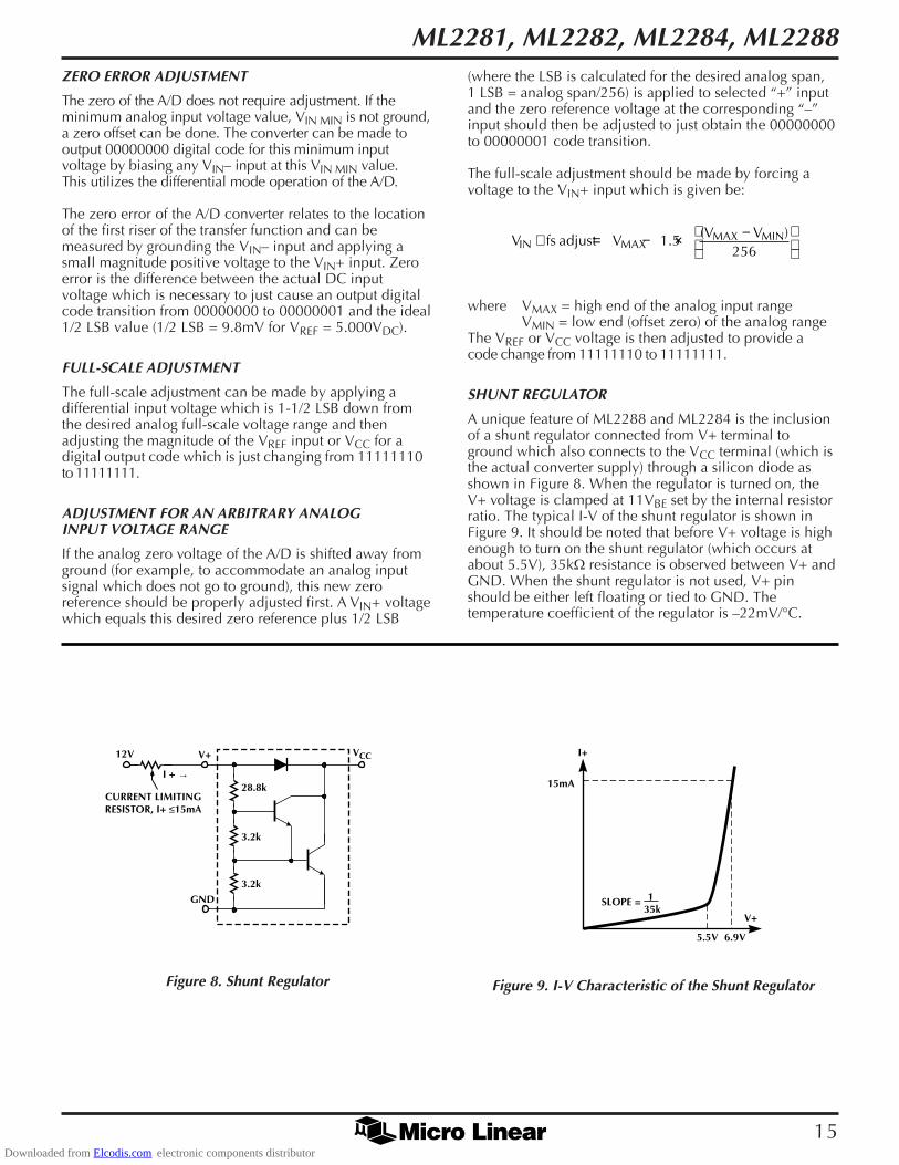
Figure 8. Shunt Regulator
I+
15mA
V+
5.5V
SLOPE =
6.9V
135k
Figure 9. I-V Characteristic of the Shunt Regulator
(where the LSB is calculated for the desired analog span,1 LSB = analog span/256) is applied to selected “+” inputand the zero reference voltage at the corresponding “–”input should then be adjusted to just obtain the 00000000to 00000001 code transition.
The full-scale adjustment should be made by forcing avoltage to the VIN+ input which is given be:
V fs adjust V V VIN MAX
MAX MIN+ = − × −
1 5256
. ( )
where VMAX = high end of the analog input rangeVMIN = low end (offset zero) of the analog range
The VREF or VCC voltage is then adjusted to provide acode change from 11111110 to 11111111.
SHUNT REGULATOR
A unique feature of ML2288 and ML2284 is the inclusionof a shunt regulator connected from V+ terminal toground which also connects to the VCC terminal (which isthe actual converter supply) through a silicon diode asshown in Figure 8. When the regulator is turned on, theV+ voltage is clamped at 11VBE set by the internal resistorratio. The typical I-V of the shunt regulator is shown inFigure 9. It should be noted that before V+ voltage is highenough to turn on the shunt regulator (which occurs atabout 5.5V), 35kW resistance is observed between V+ andGND. When the shunt regulator is not used, V+ pinshould be either left floating or tied to GND. Thetemperature coefficient of the regulator is –22mV/°C.
Downloaded from Elcodis.com electronic components distributor
ML2281, ML2282, ML2284, ML2288
16
APPLICATIONS
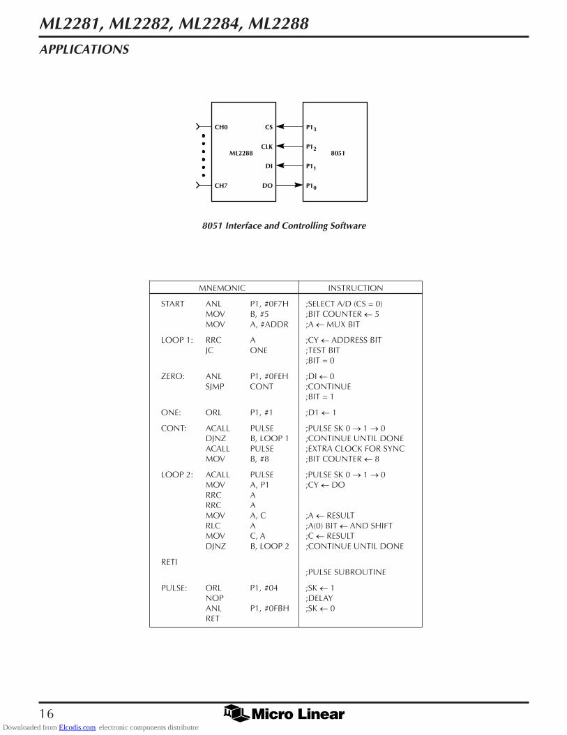
8051 Interface and Controlling Software
MNEMONIC INSTRUCTION
START ANL P1, #0F7H ;SELECT A/D (CS = 0)MOV B, #5 ;BIT COUNTER ¬ 5MOV A, #ADDR ;A ¬ MUX BIT
LOOP 1: RRC A ;CY ¬ ADDRESS BITJC ONE ;TEST BIT
;BIT = 0
ZERO: ANL P1, #0FEH ;DI ¬ 0SJMP CONT ;CONTINUE
;BIT = 1
ONE: ORL P1, #1 ;D1 ¬ 1
CONT: ACALL PULSE ;PULSE SK 0 ® 1 ® 0DJNZ B, LOOP 1 ;CONTINUE UNTIL DONEACALL PULSE ;EXTRA CLOCK FOR SYNCMOV B, #8 ;BIT COUNTER ¬ 8
LOOP 2: ACALL PULSE ;PULSE SK 0 ® 1 ® 0MOV A, P1 ;CY ¬ DORRC ARRC AMOV A, C ;A ¬ RESULTRLC A ;A(0) BIT ¬ AND SHIFTMOV C, A ;C ¬ RESULTDJNZ B, LOOP 2 ;CONTINUE UNTIL DONE
RETI;PULSE SUBROUTINE
PULSE: ORL P1, #04 ;SK ¬ 1NOP ;DELAYANL P1, #0FBH ;SK ¬ 0RET
CH0
ML2288 8051
P13
P12
P11
P10
CS
CLK
DI
DOCH7
Downloaded from Elcodis.com electronic components distributor
ML2281, ML2282, ML2284, ML2288
17
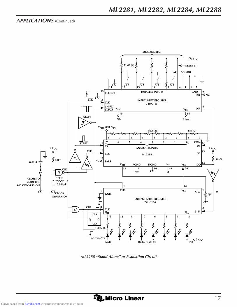
APPLICATIONS (Continued)
10kΩ
CLK
CLK
CLK
CLK
Q D
CLOCKGENERATOR
CLK
CLR
CLK
CLK
CLK INT
CLK
CS
SARS
GNDSI A
SI BCLKQH
VCC
VCC
VCCSINSHIFT/LOAD
VREF
QA
10kΩ
5 VDC
START
START
+
CLOSE TOSTART THE
A/D CONVERSION
0.01µF
0.001µF
OUTPUT SHIFT REGISTER74HC164
ANALOG INPUTS
PARALLEL INPUTS
MUX ADDRESS
GND
INPUT SHIFT REGISTER74HC165
ML2288
1 141
14
2019101112
13
17D1
COM
912345678
18
16
15NC
0123
1kΩ (8) 1/8 VCC
4567
DO
DO
DO
V+DGNDAGND
SE
+ 10µF
51kΩ
2
345610111213
7
8
1.3kΩ (8)
1/2 74HC74MSB DATA DISPLAY LSB
5VDC
5VDC
5VDC
5VDC
5VDC (OR VIN)
14
NC
10
7
76543141312
51kΩ (4)
1115
2
1 9
NC
SGL/DIF
START BIT
ML2288 “Stand-Alone” or Evaluation Circuit
Downloaded from Elcodis.com electronic components distributor
ML2281, ML2282, ML2284, ML2288
18
3kΩ
+10µF
ML2281
LM335
TA
VIN (–)
VIN (+) VCC
VCC(5 VDC)
VREF
10kΩTA MIN
ADJ.
10kΩTA MAXADJ.
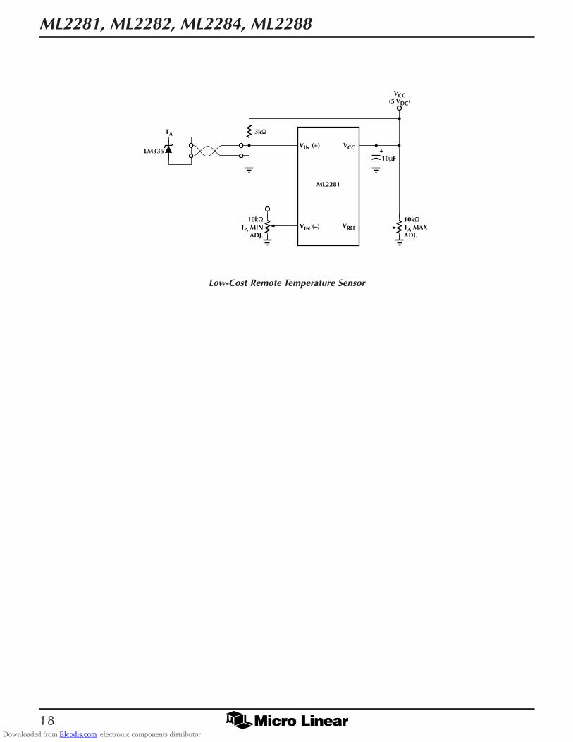
Low-Cost Remote Temperature Sensor
Downloaded from Elcodis.com electronic components distributor
ML2281, ML2282, ML2284, ML2288
19
APPLICATIONS (Continued)
10kΩFS
ADJ.
1kΩGAIN
10kΩOFFSET
DUAL
DUAL
5.1V
2.7kΩ10kΩ
10V
10V6.8kΩ
330ΩVCC
(5VDC)
1kΩ2VDC
ZERO ADJ.
++
10µF
1.2kΩ
2.7kΩ
330Ω
1kΩ
3V
VIN (+)
VIN
VCC
VCCVREF
–IN
+IN DO
CLK
CSML2281
VREF
ML2281
+1µF
SETVOLTAGE SPAN
1MΩ
VIN (–)
SETS ZEROCODE VOLTAGE
+
–
+
–
1MΩ
20kΩ
20kΩ
STRAIN GAUGELOAD CELL
300Ω/30mV FS
CH0
CH7 SERIAL I/O
COM
LM335
LM385
TL064
TL064 TL064
VREF
tREF
tREF
VCC
VCC
VCC
ML2288
+
–
+
–
+
–
+
–
+
–
910Ω
820Ω
1kΩ
1kΩTYPE J
TYPE J
T1
+
–
+
–T8
1kΩ
22kΩ
88.2kΩ
88.2k
••
•
•
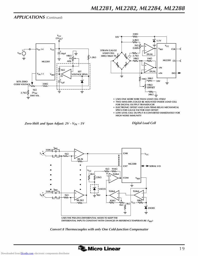
USES ONE MORE WIRE THAN LOAD CELL ITSELFTWO MINI-DIPs COULD BE MOUNTED INSIDE LOAD CELLFOR DIGITAL OUTPUT TRANSDUCERELECTRONIC OFFSET AND GAIN TRIMS RELAX MECHANICALSPECS FOR GAUGE FACTOR AND OFFSETLOW LEVEL CELL OUTPUT IS CONVERTED IMMEDIATELY FORHIGH NOISE IMMUNITY
tREF
USES THE PSEUDO-DIFFERENTIAL MODE TO KEEP THE DIFFERENTIAL INPUTS CONSTANT WITH CHANGES IN REFERENCE TEMPERATURE (TREF)
2kΩ
3kΩ20kΩ
1kΩ
Zero-Shift and Span Adjust: 2V - VIN - 5V Digital Load Cell
Convert 8 Thermocouples with only One Cold-Junction Compensator
Downloaded from Elcodis.com electronic components distributor
ML2281, ML2282, ML2284, ML2288
20
APPLICATIONS (Continued)
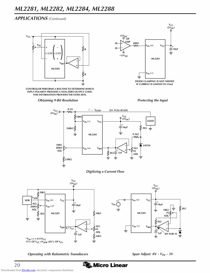
Obtaining 9-Bit Resolution
VCC
VIN VIN (+)
VIN (–)
VCC
VCC(5VDC)
–15VDC
15VDC
VREF +
–
+
–
+
–
ML2281
+
–
–
≤ 2.5V> 2.5V
+
R
R( (ML2281
+
+
10µF
OPAMP 600Ω
1µF
VIN (–)
VIN (+)
VCC
VREF
VCC(5VDC)
VCC(5VDC)
ML2281
LOAD
LM336
9.1kΩ
240kΩ
120kΩ
100Ω
0.1Ω (2A FULL-SCALE)ILOAD
2kΩ
1kΩFSADJ.
10kΩFS
ADJ.
100ΩZEROADJ.
+10µF
→
+
–
VIN (+)
*VIN (–) = 0.15VCC15% OF VCC ≤VXDR ≤85% OF VCC
VCC
VREF
VCC(5VDC)
ML2281
0.7 VCC1kΩFSADJ.
1kΩZEROADJ.
24kΩ
+10µF
+1µF
VCC(5VDC)
++
10µF
10kΩ
2kΩ
20kΩ
3kΩ
VIN (–)*
XDRVXDR
+
–
VIN (+)
VIN
VCC
VREF
ML2281
+1µF SET FOR 3V
VIN (–)
CONTROLLER PERFORMS A ROUTINE TO DETERMINE WHICHINPUT POLARITY PROVIDES A NON-ZERO OUTPUT CODE.
THIS INFORMATION PROVIDES THE EXTRA BITS.
DIODE CLAMPING IS NOT NEEDEDIF CURRENT IS LIMITED TO 25mA
3kΩ
1kΩ
Protecting the Input
Operating with Ratiometric Transducers Span Adjust: 0V - VIN - 3V
Digitizing a Current Flow
Downloaded from Elcodis.com electronic components distributor
ML2281, ML2282, ML2284, ML2288
21
APPLICATIONS (Continued)
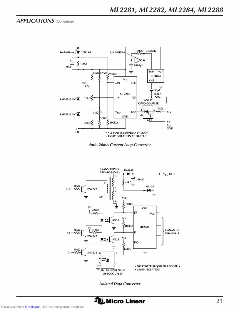
4mA–20mA Current Loop Converter
VCC
ML2281
GND
+IN
–IN
VREF DO
CS
CLK
GNDVO
VCC
V+
1000pF
100kΩ = 50kHZ
INP
CD4024
50pF
100kΩ
10kΩ235
6 8
6N139OPTO COUPLER
VCC
VO5
200kΩ6.2kΩ
3.9kΩ300kΩ47kΩ
10kΩ
5kΩ
24kΩ
47µF
10µF100Ω
+
LM385–2.5V
LM385–2.5V
4mA–20mA 1N4148 1/6 74HC14
→
→
• ALL POWER SUPPLIED BY LOOP• 1500V ISOLATION AT OUTPUT
TRANSFORMERTRW-TC-SSD-32
1N4148
1N4148
470Ω6V
6V 1
5
3
72
6
6V
10kΩDI
470Ω
100µF+
CLK
VCC
VCC
VCC
VCC
ML2288
100kΩ
2N2222
2N2222 2
3
8
6
5
2N2222
D1
DO
CS
VCC OUT
10kΩCS
10kΩCLK
6.8kΩ
8 ANALOGCHANNELS
47kΩ
4N28
4N28
• NO POWER REQUIRED REMOTELY• 1500V ISOLATION6N139 HIGH GAIN
OPTOCOUPLER
100kΩ
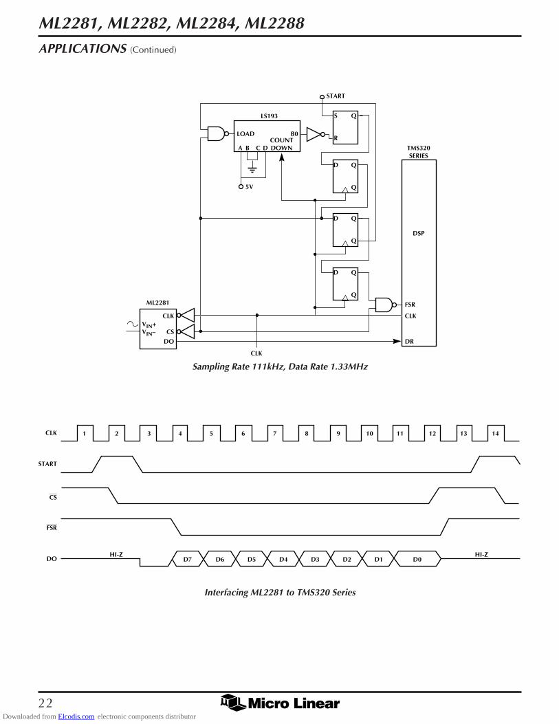
Isolated Data Converter
Downloaded from Elcodis.com electronic components distributor
ML2281, ML2282, ML2284, ML2288
22
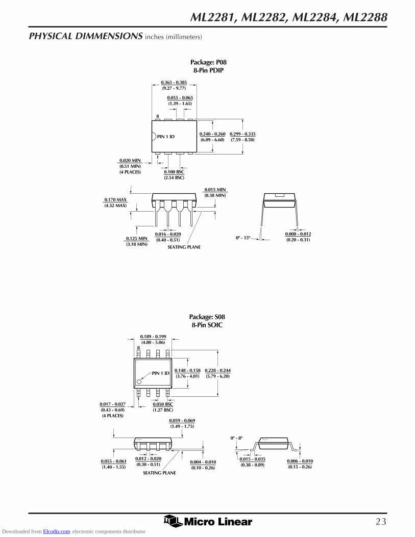
APPLICATIONS (Continued)
D Q
Q
D Q
Q
D Q
Q
S
R
Q
DSP
LS193
COUNTDOWN
ML2281 FSR
START
CLKVIN+VIN–
LOAD
A
5V
B C D
B0
CLK
DRDO
CS
CLK
TMS320SERIES
CLK 1
D7 D6 D5 D4 D3 D2 D1 D0
2 3 4 5 6 7 8 9 10 11 12 13 14
START
CS
FSR
DOHI-Z HI-Z
Interfacing ML2281 to TMS320 Series
Sampling Rate 111kHz, Data Rate 1.33MHz
Downloaded from Elcodis.com electronic components distributor
ML2281, ML2282, ML2284, ML2288
23
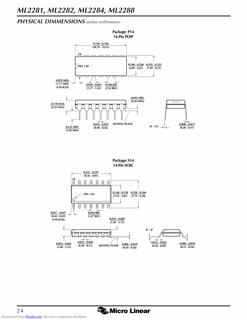
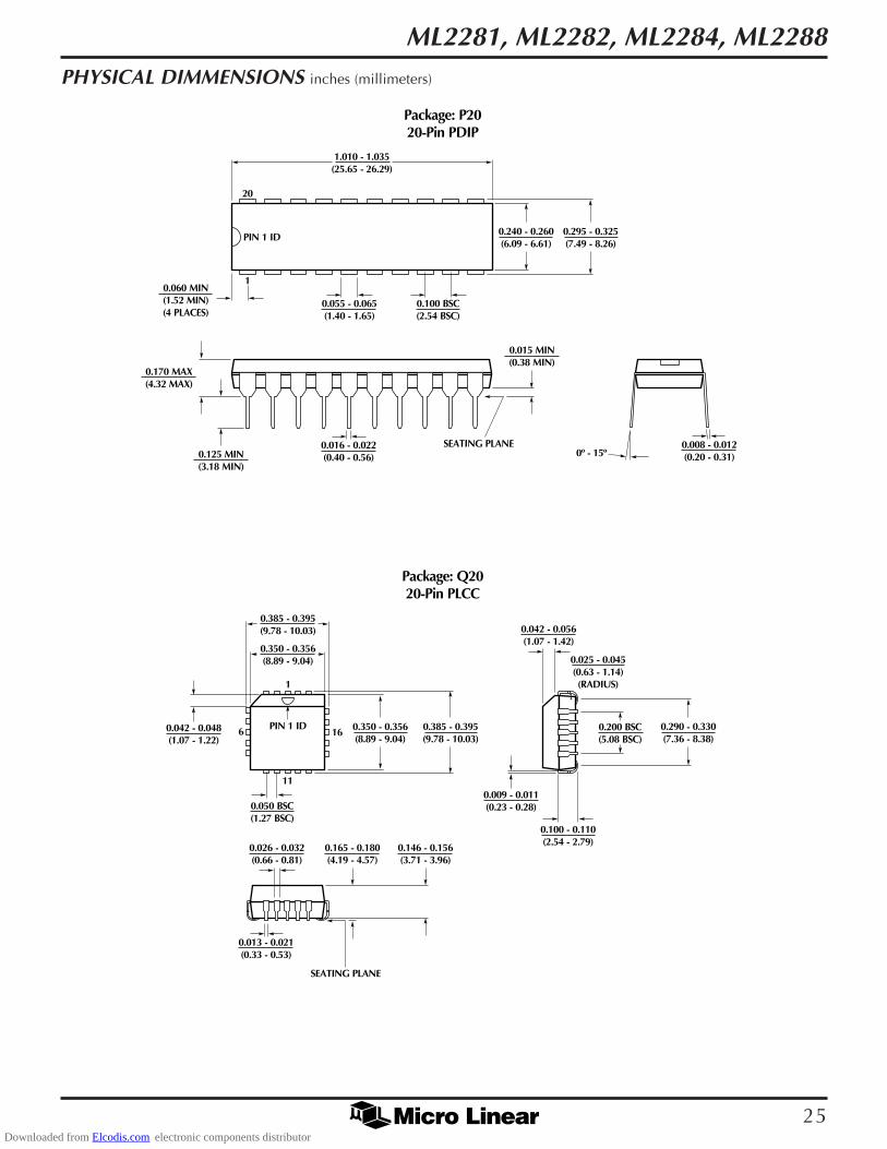
PHYSICAL DIMMENSIONS inches (millimeters)
SEATING PLANE
0.240 - 0.260(6.09 - 6.60)
PIN 1 ID 0.299 - 0.335(7.59 - 8.50)
0.365 - 0.385(9.27 - 9.77)
0.016 - 0.020(0.40 - 0.51)
0.100 BSC(2.54 BSC)
0.008 - 0.012(0.20 - 0.31)
0.015 MIN(0.38 MIN)
8
0º - 15º
1
0.055 - 0.065(1.39 - 1.65)
0.170 MAX(4.32 MAX)
0.125 MIN(3.18 MIN)
0.020 MIN(0.51 MIN)(4 PLACES)
Package: P088-Pin PDIP
SEATING PLANE
0.148 - 0.158(3.76 - 4.01)
PIN 1 ID0.228 - 0.244(5.79 - 6.20)
0.189 - 0.199(4.80 - 5.06)
0.012 - 0.020(0.30 - 0.51)
0.050 BSC(1.27 BSC)
0.015 - 0.035(0.38 - 0.89)
0.059 - 0.069(1.49 - 1.75)
0.004 - 0.010(0.10 - 0.26)
0.055 - 0.061(1.40 - 1.55)
8
0.006 - 0.010(0.15 - 0.26)
0º - 8º
10.017 - 0.027(0.43 - 0.69)(4 PLACES)
Package: S088-Pin SOIC
Downloaded from Elcodis.com electronic components distributor
ML2281, ML2282, ML2284, ML2288
24
SEATING PLANE
0.148 - 0.158(3.76 - 4.01)
PIN 1 ID0.228 - 0.244(5.79 - 6.20)
0.337 - 0.347(8.56 - 8.81)
0.012 - 0.020(0.30 - 0.51)
0.050 BSC(1.27 BSC)
0.015 - 0.035(0.38 - 0.89)
0.059 - 0.069(1.49 - 1.75)
0.004 - 0.010(0.10 - 0.26)
0.055 - 0.061(1.40 - 1.55)
14
0.006 - 0.010(0.15 - 0.26)
0º - 8º
10.017 - 0.027(0.43 - 0.69)(4 PLACES)
Package: S1414-Pin SOIC
PHYSICAL DIMMENSIONS inches (millimeters)
SEATING PLANE
0.240 - 0.260(6.09 - 6.61)
PIN 1 ID 0.295 - 0.325(7.49 - 8.25)
0.740 - 0.760(18.79 - 19.31)
0.016 - 0.022(0.40 - 0.56)
0.100 BSC(2.54 BSC)
0.008 - 0.012(0.20 - 0.31)
0.015 MIN(0.38 MIN)
14
0º - 15º
1
0.050 - 0.065(1.27 - 1.65)
0.170 MAX(4.32 MAX)
0.125 MIN(3.18 MIN)
0.070 MIN(1.77 MIN)(4 PLACES)
Package: P1414-Pin PDIP
Downloaded from Elcodis.com electronic components distributor
ML2281, ML2282, ML2284, ML2288
25
PHYSICAL DIMMENSIONS inches (millimeters)
SEATING PLANE
0.240 - 0.260(6.09 - 6.61)
PIN 1 ID 0.295 - 0.325(7.49 - 8.26)
1.010 - 1.035(25.65 - 26.29)
0.016 - 0.022(0.40 - 0.56)
0.100 BSC(2.54 BSC)
0.008 - 0.012(0.20 - 0.31)
0.015 MIN(0.38 MIN)
20
0º - 15º
1
0.055 - 0.065(1.40 - 1.65)
0.170 MAX(4.32 MAX)
0.125 MIN(3.18 MIN)
0.060 MIN(1.52 MIN)(4 PLACES)
Package: P2020-Pin PDIP
0.100 - 0.110(2.54 - 2.79)
PIN 1 ID
SEATING PLANE
0.385 - 0.395(9.78 - 10.03)
0.350 - 0.356(8.89 - 9.04)
0.013 - 0.021(0.33 - 0.53)
0.165 - 0.180(4.19 - 4.57)
1
0.350 - 0.356(8.89 - 9.04)
0.385 - 0.395(9.78 - 10.03)
6
11
16 0.290 - 0.330(7.36 - 8.38)
0.025 - 0.045(0.63 - 1.14)(RADIUS)
0.009 - 0.011(0.23 - 0.28)
0.026 - 0.032(0.66 - 0.81)
0.042 - 0.048(1.07 - 1.22)
0.042 - 0.056(1.07 - 1.42)
0.200 BSC(5.08 BSC)
Package: Q2020-Pin PLCC
0.146 - 0.156(3.71 - 3.96)
0.050 BSC(1.27 BSC)
Downloaded from Elcodis.com electronic components distributor
ML2281, ML2282, ML2284, ML2288
26
Micro Linear reserves the right to make changes to any product herein to improve reliability, function or design.Micro Linear does not assume any liability arising out of the application or use of any product described herein,neither does it convey any license under its patent right nor the rights of others. The circuits contained in thisdata sheet are offered as possible applications only. Micro Linear makes no warranties or representations as towhether the illustrated circuits infringe any intellectual property rights of others, and will accept no responsibilityor liability for use of any application herein. The customer is urged to consult with appropriate legal counselbefore deciding on a particular application.
5/5/97 Printed in U.S.A.
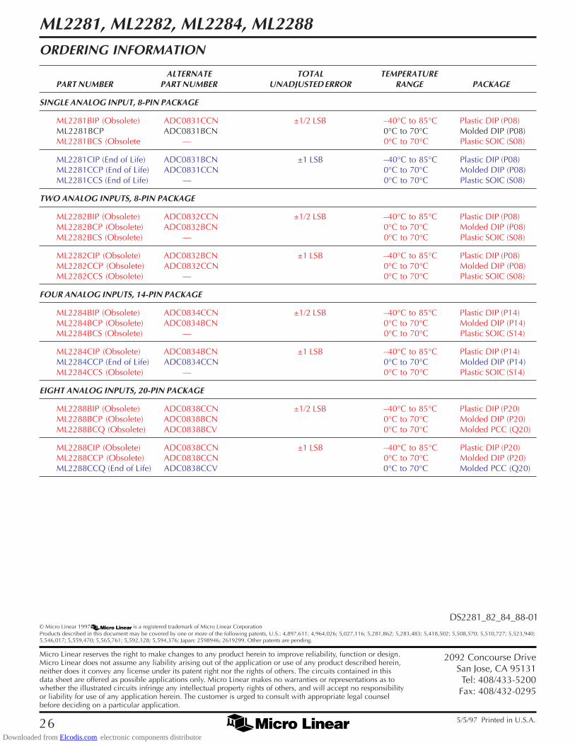
ORDERING INFORMATION
ALTERNATE TOTAL TEMPERATUREPART NUMBER PART NUMBER UNADJUSTED ERROR RANGE PACKAGE
SINGLE ANALOG INPUT, 8-PIN PACKAGE
ML2281BIP (Obsolete) ADC0831CCN ±1/2 LSB –40°C to 85°C Plastic DIP (P08)ML2281BCP ADC0831BCN 0°C to 70°C Molded DIP (P08)ML2281BCS (Obsolete — 0°C to 70°C Plastic SOIC (S08)
ML2281CIP (End of Life) ADC0831BCN ±1 LSB –40°C to 85°C Plastic DIP (P08)ML2281CCP (End of Life) ADC0831CCN 0°C to 70°C Molded DIP (P08)ML2281CCS (End of Life) — 0°C to 70°C Plastic SOIC (S08)
TWO ANALOG INPUTS, 8-PIN PACKAGE
ML2282BIP (Obsolete) ADC0832CCN ±1/2 LSB –40°C to 85°C Plastic DIP (P08)ML2282BCP (Obsolete) ADC0832BCN 0°C to 70°C Molded DIP (P08)ML2282BCS (Obsolete) — 0°C to 70°C Plastic SOIC (S08)
ML2282CIP (Obsolete) ADC0832BCN ±1 LSB –40°C to 85°C Plastic DIP (P08)ML2282CCP (Obsolete) ADC0832CCN 0°C to 70°C Molded DIP (P08)ML2282CCS (Obsolete) — 0°C to 70°C Plastic SOIC (S08)
FOUR ANALOG INPUTS, 14-PIN PACKAGE
ML2284BIP (Obsolete) ADC0834CCN ±1/2 LSB –40°C to 85°C Plastic DIP (P14)ML2284BCP (Obsolete) ADC0834BCN 0°C to 70°C Molded DIP (P14)ML2284BCS (Obsolete) — 0°C to 70°C Plastic SOIC (S14)
ML2284CIP (Obsolete) ADC0834BCN ±1 LSB –40°C to 85°C Plastic DIP (P14)ML2284CCP (End of Life) ADC0834CCN 0°C to 70°C Molded DIP (P14)ML2284CCS (Obsolete) — 0°C to 70°C Plastic SOIC (S14)
EIGHT ANALOG INPUTS, 20-PIN PACKAGE
ML2288BIP (Obsolete) ADC0838CCN ±1/2 LSB –40°C to 85°C Plastic DIP (P20)ML2288BCP (Obsolete) ADC0838BCN 0°C to 70°C Molded DIP (P20)ML2288BCQ (Obsolete) ADC0838BCV 0°C to 70°C Molded PCC (Q20)
ML2288CIP (Obsolete) ADC0838CCN ±1 LSB –40°C to 85°C Plastic DIP (P20)ML2288CCP (Obsolete) ADC0838CCN 0°C to 70°C Molded DIP (P20)ML2288CCQ (End of Life) ADC0838CCV 0°C to 70°C Molded PCC (Q20)
2092 Concourse DriveSan Jose, CA 95131Tel: 408/433-5200Fax: 408/432-0295
© Micro Linear 1997 is a registered trademark of Micro Linear CorporationProducts described in this document may be covered by one or more of the following patents, U.S.: 4,897,611; 4,964,026; 5,027,116; 5,281,862; 5,283,483; 5,418,502; 5,508,570; 5,510,727; 5,523,940;5,546,017; 5,559,470; 5,565,761; 5,592,128; 5,594,376; Japan: 2598946; 2619299. Other patents are pending.
DS2281_82_84_88-01
Downloaded from Elcodis.com electronic components distributor