ming hsieh department of electrical...
TRANSCRIPT
Ming Hsieh Department of Electrical EngineeringEE 459Lx - Embedded Systems Design Laboratory
Using the I2C Interface on theATmega328P and MC908JL16
by
Allan G. Weber
1 IntroductionThis document is intended for students in EE109L (Introduction to Embedded Systems) and EE459Lx(Embedded Systems Design Laboratory) and is meant to serve the following purposes.
• An introduction to the I2C protocol.
• A description of how to use the “i2c_io” C function for I2C data transfers.
• A short tutorial on how to configure the oscilloscopes in the labs for debugging I2C data transfers.
The I2C or I2C (Inter-Integrated Circuit ) interface is a serial bus intended for communication betweentwo or more integrated circuits on the same PC or prototyping board. Also known as a “two-wire bus”, thisbus is for communication with many different types of IC’s such as EEPROMs, real-time clock, temperaturesensors, etc. The I2C interface is not particularly fast so it is typically used for connecting to IC’s that donot require large amounts of data to be transferred rapidly.
Some of the microcontrollers used in EE109L and EE459Lx such as the Atmel ATmega328P and theFreescale MC908JL16 implement this interface in hardware. The Atmel documentation calls the I2C interfacethe “Two Wire Interface" while the Freescale documentation refers to it as “MMIIC” (Multi-Master IIC) butit’s the same thing.
The hardware on these microcontrollers perform many of the lower level tasks required for transferringdata on the I2C bus. For example, to write data to a I2C device, the program sets up the transfer, startsit, keeps a data buffer full with the next byte to be sent and finally terminates the transfer at the end. Thesignaling required for sending each bit is handled by the hardware. Reading is done in a similar manner.
Software-only implementations of the I2C protocol can also be used to provide this interface on micro-controllers that do not have I2C hardware.
The Agilent and Tektronix oscilloscopes in OHE 240 and the Keysight scopes in VHE 205 lab have specialtriggering capabilities that make it possible to analyze I2C data transfers. Individual data transfers can becaptured and viewed so that the transfer can be examined in detail to see if the correct information is beingsent or received. This capability of these scopes is an extremely useful tool for students trying to debug anyI2C aspects of their projects.
2 The I2C BusI2C devices communicate over a shared two wire bus. One wire is for the clock signal and the other is forthe data. In our typical configurations, the microcontroller is the bus master and generates the clock signal.Depending on which way the data is being transferred, either the bus master (the microntroller) or one ofthe slave devices generates the signal that is placed on the bi-directional data line. Figure 1 show a typical
EE 459Lx, Rev. 4/20/17 1

SDASCLWP
A0A1A2
567
123
24LC256SDASCL VBAT
56
3DS1307
SDASCL
A0A1A2
765
12
DS1621
10kΩ
+5 +5
X1 X21 2
32kHzXTAL
PC4PC5
2728
AtmelATmega328P
Figure 1: Typical I2C bus
configuration with a microcontroller attached to three different devices (an EEPROM, a real-time-clock anda temperate sensor) by an I2C bus.
To allow multiple devices to share the same bus, all the I2C devices attached to the bus must use “opendrain” connections to both the clock and data lines. A device that needs to transfer data can either pull theline to ground (logical zero), or let it float in which case it will be pulled up to the power supply voltage(logical one) by the attached pull-up resistor. The pull-up resistors are usually in the range of 5kΩ to 10kΩand one is needed for each of the two bus lines.
Important: An I2C bus will not operate without the pull-up resistors. When there is no activity on thebus, the clock and data lines must be in the high (logical one) state. If this is not the case, the data transferscan not be initiated. When debugging I2C hardware this is the first thing to check: are the clock and datalines high when no transfers are taking place? Both lines must be high before the transfer, and both mustreturn to the high state after the transfer is complete.
3 I2C Devices and Data TransfersThe following sections describe how I2C devices are identified on an I2C bus and and overview of how writingand reading operations are performed.
3.1 Device AddressesAll devices attache to an I2C bus have a address that is used to identify the device on the bus. This isusually referred to as the “device address” and is fixed by the manufacturer of the device. In many cases itcan not be changed by the user although some devices allow it to be customized slightly as described below.In order to use the I2C interface you need to know the address of the device on the I2C bus.
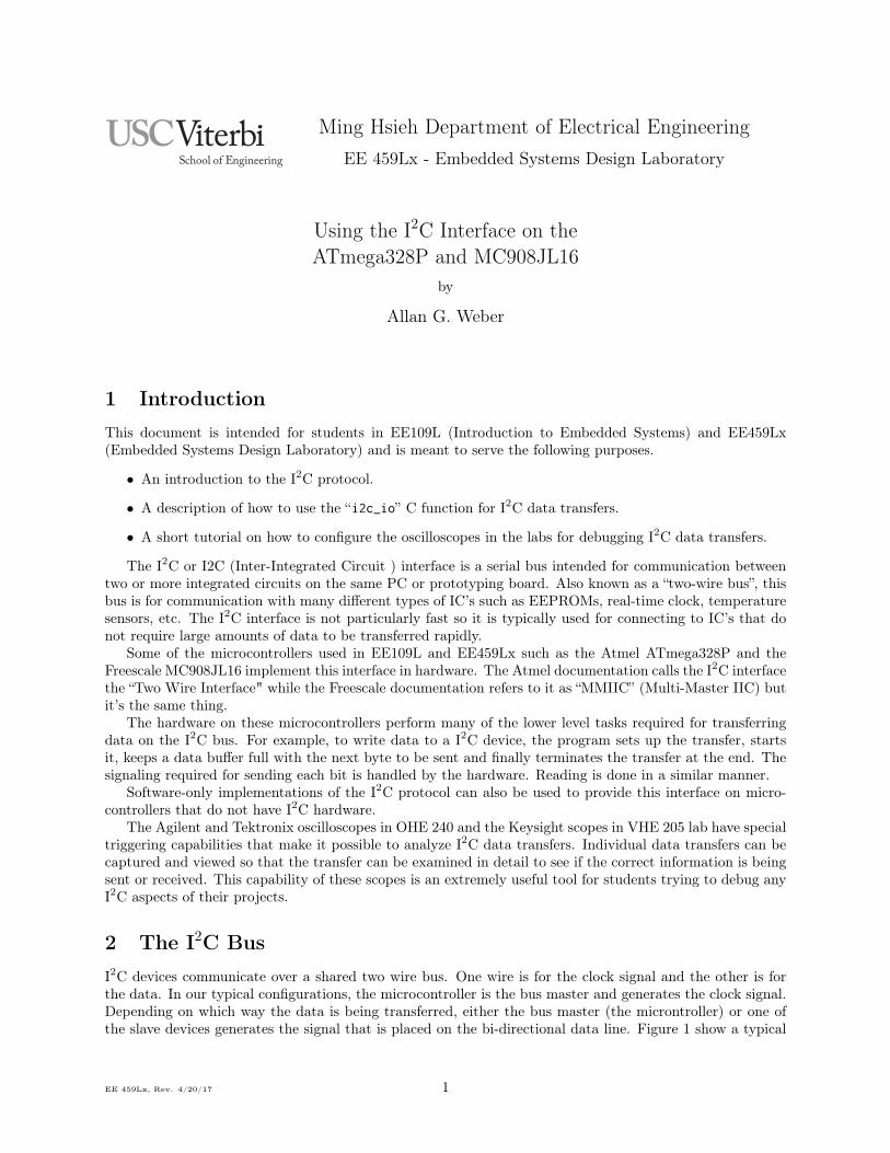
The specification of the address is a common source of confusion since some datasheets list it as a seven-bit number and others as an eight-bit number. The actual address is a seven bit number but it is oftencombined with an additional bit in the least significant bit position to create an eight-bit number. Theupper seven bits are the address and the least significant bit indicates whether a read or write is occurring.An example of this is shown in Fig. 2. An I2C chip might have a seven-bit address of 0x5C, but this can alsobe listed as the eight-bit address 0xB8.
When searching for the address in the manufacturer’s datasheets it’s very important to figure out whichformat they are using for the address. Often the datasheet will not explicitly state that the address is theseven or eight bit address. In these cases the only solution may be to try both addresses in the software andsee which one appears to work. Table 1 shows the 8-bit value (7-bit address + R/W flag) for some commondevices used in projects.
Some I2C devices allow you to specify one or more of the least significant bits of the seven-bit addressby connecting pins on the chip to a logical zero or one. This make it possible to have more than one device
EE 459Lx, Rev. 4/20/17 2
1 0 1 1 1 0 0 0
Seven-bit address 0x5C
Eight-bit address 0xB8
5 C
B 8
Figure 2: 7-bit and 8-bit I2C addresses
of the same type on the bus or to avoid address conflicts with other devices. The number of extra addressbits available is indicated in Table 1.
I2C Device Description 8-bit Device Number of ExtraAddress Address Bits
24LC256 32KB EEPROM 0xA0 3DS1307 Real-time clock 0xD0 nonePCF8563 Real-time clock 0xA2 noneDS1621, DS1631 Temperature sensor 0x90 3MCP23008 8-bit port expander 0x40 3MCP23017 16-bit port expander 0x40 3MAX7311 16-bit port expander 0x40 3HMC5883L Magnetic sensor 0x3C noneMPL3115A2 Altimeter/thermometer 0xC0 noneLIS3DH Accelerometer 0x30 none
Table 1: I2C Device Addresses
3.2 Writing DataWriting to an I2C device is usually done in two steps but these can normally be done as one single writeoperation. Many I2C devices consist of a number of registers or memory locations that can be written toand the first step is to send the address of the first location in the device that data is to be written to. Thesecond part of the write operation is to send the data that goes in the addressed location. Most I2C deviceswill automatically increment the internal address after each byte is written to it, so it’s only necessary toaddress the first location and all the data then written to it will be stored in consecutive locations.
For example, to write the bytes 0xAA, 0xBB and 0xCC to location 5, 6 and 7 in a device, the programwould send the data: 0x05, 0xAA, 0xBB, 0xCC. The 0xAA will be stored in location 5, the 0xBB in location 6,and the 0xCC in location 7.
Some devices that have a large number of internal memory locations may require sending a two-byteaddress instead of a one-byte address as shown in the example above. In this case the operation is the sameexcept two bytes of address data must precede the byte to be written.
This concept of the device’s internal addresses is often a source of confusion for users. It’s important tounderstand the difference between the “device address” that identifies the I2C device on the bus, and the“internal address” that specifies where in the device data will be written to (or read from.)
3.3 Reading DataMany I2C devices require reading operations to be done in two steps. The first part of the reading operationconsists of a write operation as described above where the address of the first location to be read is sentto the device. Depending on the device this might be a single address byte or it could be multiple bytes.However instead of then sending the data to be written starting at that location, the write operation is
EE 459Lx, Rev. 4/20/17 3

terminated and a read command is sent. This causes the device to start sending data from the locationgiven by the address data that was previously written to it. As with a write operation, the internal addressis automatically incremented as data is read and the program can read as many consecutive locations asneeded.
4 Initializing the I2C Modules
4.1 ATmega328PThe ATmega328P uses pins 27 and 28 for the I2C data and clock. When I2C is not used these pins can beused as general I/O ports PC4 and PC5.
The internal I2C hardware needs to have the baud rate (I2C clock rate) set before any transfers can takeplace. The maximum rate that the I2C device can handle should be described in the device’s datasheet,but most devices should be able to operate with a clock up to 100kHz. The clock is derived from themicrocontroller’s clock by dividing it down according to this formula.
I2C Baud Rate =CPU Clock Frequency
16 + 2(TWBR) · (prescalar value)
The prescalar value is set by a two bit number in the TWSR register and can be either 1, 4, 16 or 64. TheTWBR value is the eight-bit contents of the TWBR register. This value can be calculated if we rearrange theabove formula to solve for TWBR
TWBR =
(CPU Clock Frequency
I2C Baud Rate
)− 16)/(2 · prescalar value)
A suitable value for TWBR can be calculated in the program source code using compiler preprocessorstatements. For example, if we want a baud rate of 100kHz, we can set the prescalar to one and then usethe following to determine the value to go in the TWBR register.
#define FOSC 9830400 // Clock frequency = Oscillator freq.#define BDIV (FOSC / 100000 - 16) / 2 + 1
TWSR = 0; // Set prescalar for 1TWBR = BDIV; // Set bit rate register
The +1 at the end of the statement calculating BDIV is needed since the integer calculations done bythe preprocessor could have truncation errors resulting in a value of BDIV that is too low and giving an I2Cfrequency over 100kHz. The +1 makes sure the frequency is below 100kHz.
The software provided for I2C on the ATmega328P includes function that can be called to do the ini-tialization. The routine take the value to go into the bit rate register (BDIV in the example above) as itsargument. The following is an example of how it can be used.
#define FOSC 9830400#define BDIV (FOSC / 100000 - 16) / 2 + 1
i2c_init(BDIV)
4.2 MC908JL16The JL16 has two pairs of pins, 13 and 14 or 8 and 9, that can be used as the I2C interface. The selectionof which pair to use is determined by the IICSEL bit in the CONFIG2 register. If the bit is left in the defaultsetting of zero, the I2C interface uses pins 13 and 14 for the data and clock. If pins 13 and 14 need to beused for other purposes such as I/O ports PTD6 and PTD7 or for the for the SCI functions the I2C functionscan be moved to pins 8 and 9 with the command
CONFIG2_IICSEL = 1; // I2C on PTA2 ,3
EE 459Lx, Rev. 4/20/17 4

Before using the I2C hardware, the program must set the baud rate (I2C clock rate) to be used. Themaximum rate that the I2C device can handle should be described in the device’s datasheet, but most devicesshould be able to operate with a clock up to 100kHz. The clock is derived from the microcontroller’s clockby dividing it down. The divisor is determined a three bit number stored in the MIMCR register according tothe formula
divisor = 2n+5
where n is a three bit number from 0 to 7. This results in divisor values from 32 to 4096. For example, ifthe oscillator’s frequency is 9.8304MHz and we use a divisor value of 3, this will result in a I2C baud rate of38.4kHz.
Once the divisor is set, the I2C interface is enabled by setting the MMEN bit in the MMCR register.
MIMCR_MMBR = 3; // Set baud rate divisorMMCR_MMEN = 1; // Enable MMIIC
The software provided for I2C on the MC908JL16 includes function that can be called to do the initial-ization. The routine take the value to go into the baud rate register as its argument. The following is anexample of how it can be used with the value determined above.
i2c_init (3)
EE 459Lx, Rev. 4/20/17 5

5 Using the i2c_io I2C Interface RoutineA C function, i2c_io, has been written to hopefully simplify doing reads and writes to I2C devices. Thisfunction combines the operations of reading and writing into a single function since the nature of how readsand writes are done with I2C results in a lot of commonality between the operations.
The function interface is based on three arrays of bytes. The first array contains the internal addressvalues that are written to the device before any data bytes are written or read. The second array containsany data that is to be written to the device. The third array is where data read from the device is stored.
The function is called in the following manner.
status = i2c_io(DEV_ADDR , abuf , na, wbuf , nw, rbuf , nr);
where “abuf”, “wbuf” and “rbuf” are the three arrays, and “na”, “nw” and “nr” are the number bytes to writefrom or read in to each respectively. If the count value for any of the arrays is zero, nothing is written fromor read into that array. The function return value is zero if there were no errors. A non-zero value indicatesome type of error occurred.
The following code segment show how to write four bytes of data to a device at 8-bit I2C device address0xAC with the internal address for the write starting at 9.
unsigned char status;unsigned char addr = 9;unsigned char buf[4] = 1, 2, 3, 4 ;
status = i2c_io (0xAC , &addr , 1, buf , 4, NULL , 0);
Note that the address data had to be passed as a pointer to the variable containing the address since theroutines expects all the data to be bytes in arrays.
The data in the “abuf” and “wbuf” arrays are both written to the device, in that order, so there is noactual difference between sending data by putting it in one array or the other. The three lines of code belowall do exactly the same thing.
i2c_io (0xA0 , buf , 100, NULL , 0, NULL , 0);i2c_io (0xA0 , NULL , 0, buf , 100, NULL , 0);i2c_io (0xA0 , buf , 2, buf+2, 98, NULL , 0);
In all cases the first 100 bytes from array "buf" will be written to the I2C device at bus address 0xA0. Theonly reason for the separate “abuf” and “wbuf” arrays is so that the address data can be taken from onearray (abuf), and then the write data from another (wbuf) without requiring that the contents be mergedinto one array before calling the function.
The following code segment show how to read 32 bytes of data from a device at 8-bit I2C device address0x70 with the internal address for starting the reading specified by the two byte value 0x0120.
unsigned char status;unsigned char abuf = 0x01 , 0x20;unsigned char rbuf [32];
status = i2c_io (0x70 , abuf , 2, NULL , 0, rbuf , 32);
For more information on using the i2c_io routine see the comments at the beginning of the functionsource code.
EE 459Lx, Rev. 4/20/17 6

6 Viewing I2C Transfers on the Keysight MSO-X 3024A ScopesThe Keysight (ex-Agilent) MSO-X 3024A oscilloscopes have I2C triggering as part of the EMBD option. Tomake use of this follow the steps below. If at any time during the setup you want to make a menu disappearfrom the screen, press the “Back” button near the lower right corner of the screen.
1. Turn on the scope and then turn on two of four input channels by pressing the buttons with numberson them in the vertical section of controls until the traces appear on the screen (Fig. 3). In this examplewe’ll use channels 1 and 2.
2. Use the large knobs above the “1” and “2” buttons to adjust the input levels for both channels to 5Volts per division. The levels for the channels are shown in the upper left part of the screen.
3. Use the small knobs below channel buttons to vertically position the two traces on the screen whereboth can be viewed.
4. Use the large knob in the horizontal section of the controls to change the horizontal sweep speed to200µs (time/division). The sweep speed is shown in the upper right portion of the screen.
5. The small knob in the right part of the horizontal section changes the horizontal position of thedisplayed signal. First press the knob to center the signal on the screen, and then rotate the knob tomove the small orange triangle at the top of the screen over closer to the left side of the screen. Whenan I2C signal is captured, it will be displayed with the starting point of the signal at this position.
6. Connect two scope probes to channels 1 and 2 of the scope and then connect the probe tips to the I2Cclock and data lines on your project board. Either one can be attached to either signal but make noteof which way they are connected.
7. The Keysight scopes can have two stored configurations for working with serial signals like I2C. Tosetup a one for I2C, press the “Serial” button in right portion of the screen. This brings up the SerialDecode Menu along the bottom of the screen. Press the left soft key and it should show the two Serialselections. If Serial 1 doesn’t have the box next to it filled in with a blue square, press the buttonagain to select it.
8. The label for the second softkey from the left shows the current protocol selection for the bus. Ifit doesn’t say “I2C”, press the softkey below the label to bring up a vertical menu for selecting theprotocol type. Using the knob with the illuminated green arrow just to the right of the screen, selectthe “I2C” setting for Serial 1 as shown in Fig. 4.
Figure 3: Keysight channel settings Figure 4: Keysight serial mode set for I2C
EE 459Lx, Rev. 4/20/17 7

Figure 5: Keysight I2C input settings Figure 6: Keysight I2C signal display
9. Press the third softkey from the left labeled “Signals”. This brings up the screen shown in Fig. 5. Thecurrent settings for which channel is clock (SCL) and which is data (SDA) is shown along the bottomof the screen. Use the softkeys below the channel destinations and the selector knob to change theseto match how you connected the probes to the hardware under test.
10. For each channel, press the “Threshold” softkeys and then use the selector knob to adjust the voltagethresholds. The thresholds need to be set to something around the middle of the zero to 5 volt range.Use the selector knob to set each of the thresholds to 2.4 to 2.6 Volts
11. Press the “Trigger” button in the Trigger section of the controls. Press the “Trigger Type” soft keyto bring up the vertical menu of triggering types, and use the selector knob to scroll down near thebottom and select “Serial 1”.
12. The “Trigger on:” softkey is used to select the I2C condition that will cause the scope to acquire data.For most purposes a “Start” condition works best. If the softkey doesn’t say “Start”, press it to bringup the “Trigger on:” menu and use the selector knob to set it for triggering on an I2C Start condition.
13. Press the “Mode/Coupling” button in the Triggers section of the controls. Use the left softkey thatsays Mode to set the triggering mode to “Normal”.
At this point the scope is configured to trigger on a I2C Start condition. Press the “Single” button in theupper right to put the scope in a state where it will wait for the next Start condition on the I2C bus andthen capture the data. Do whatever is needed on your project board to get it to generate the I2C transfer,and once the data has been captured it will be displayed on the screen (Fig. 6). The captured data canbe expanded or shrunk horizontally using the horizontal scale control. The smaller knob in the horizontalsection can be used to move the display left or right to see all parts of the I2C data.
The bottom portion of the screen should show the contents of each byte in the the I2C transfer inhexadecimal. In addition it will mark various protocol bits in the transfer: S = Start, R = read, W = write,a = ACK.
EE 459Lx, Rev. 4/20/17 8
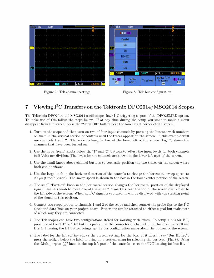
Figure 7: Tek channel settings Figure 8: Tek bus configuration
7 Viewing I2C Transfers on the Tektronix DPO2014/MSO2014 Scopes
The Tektronix DPO2014 and MSO2014 oscilloscopes have I2C triggering as part of the DPO2EMBD option.To make use of this follow the steps below. If at any time during the setup you want to make a menudisappear from the screen, press the “Menu Off” button near the lower right corner of the screen.
1. Turn on the scope and then turn on two of four input channels by pressing the buttons with numberson them in the vertical section of controls until the traces appear on the screen. In this example we’lluse channels 1 and 2. The wide rectangular box at the lower left of the screen (Fig. 7) shows thechannels that have been turned on.
2. Use the large “Scale” knobs below the “1” and “2” buttons to adjust the input levels for both channelsto 5 Volts per division. The levels for the channels are shown in the lower left part of the screen.
3. Use the small knobs above channel buttons to vertically position the two traces on the screen whereboth can be viewed.
4. Use the large knob in the horizontal section of the controls to change the horizontal sweep speed to200µs (time/division). The sweep speed is shown in the box in the lower center portion of the screen.
5. The small “Position” knob in the horizontal section changes the horizontal position of the displayedsignal. Use this knob to move one of the small “T” markers near the top of the screen over closer tothe left side of the screen. When an I2C signal is captured, it will be displayed with the starting pointof the signal at this position.
6. Connect two scope probes to channels 1 and 2 of the scope and then connect the probe tips to the I2Cclock and data lines on your project board. Either one can be attached to either signal but make noteof which way they are connected.
7. The Tek scopes can have two configurations stored for working with buses. To setup a bus for I2C,press one of the “B1” or “B2” buttons just above the connector of channel 1. In this example we’ll useBus 1. Pressing the B1 button brings up the bus configuration menu along the bottom of the screen.
8. The label for the left softkey shows the current setting for the bus. If it doesn’t say “Bus B1 I2C”,press the softkey below the label to bring up a vertical menu for selecting the bus type (Fig. 8). Usingthe “Multipurpose a” knob in the top left part of the controls, select the “I2C” setting for bus B1.
EE 459Lx, Rev. 4/20/17 9

Figure 9: Tek channel selection Figure 10: Tek trigger conditions
9. Press the second softkey from the left labeled “Define Inputs”. This brings up the screen shown inFig. 9. The current settings for which channel is clock and which is data is shown at the right side ofthe screen. Use the a and b Multipurpose knobs to change these to match how you connected theprobes to the hardware under test.
10. Press the “Thresholds” softkey to see the voltages threshold settings for each channel. The thresholdsneed to be set to something around the middle of the zero to 5 volt range. Use the two Multipurposecontrols to set each of the thresholds to 2.4 or 2.6 Volts
11. Use the “Include R/W in address” softkey to change that setting to “Yes". This will make the scope dis-play the device addresses as a eight-bit number with the least significant bit representing the read/writeflag.
12. Use the “Bus Display” softkey to change that setting to “Hex”. This causes the bytes of data on thebus to be displayed in hexadecimal rather than as binary numbers.
13. Press the “Menu” button in the Trigger section. If the “Type” softkey label doesn’t say “Bus”, press itand use the Multipurpose a knob to scroll down to “Bus”.
14. The “Trigger On” softkey is used to select the I2C condition that will cause the scope to acquire data.For most purposes a “Start” condition works best. If the softkey doesn’t say “Start”, press the softkeyto bring up the “Trigger On” menu (Fig. 10) and use the Multipurpose a knob to set it for triggeringon a I2C Start condition.
15. If the right softkey along the bottom doesn’t say “Mode Normal . . . ”, press it and then press the softkeyalong the right side to set the trigger mode for “Normal”.
16. If needed press “Menu Off” a few times to remove the menus from the screen.
At this point the scope is configured to trigger on a I2C Start condition. Press the “Single” button abovethe triggering controls to put the scope in a state where it will wait for the next Start condition on the I2Cbus and then capture the data. Do whatever is needed on your project board to get it to generate the I2Ctransfer, and once the data has been captured it will be displayed on the screen. The captured data canbe expanded or shrunk horizontally using the smaller inner knob of the “Wave Inspector” control in the topmiddle portion of the front panel. To scroll the data left or right, use the larger outer part of this control.
EE 459Lx, Rev. 4/20/17 10

Figure 11: Agilent triggering controls Figure 12: Agilent trigger Mode menu
8 Viewing I2C Transfers on the Agilent 54622A ScopesThe Agilent 54622A oscilloscopes have I2C triggering built in to them. To make use of this follow the stepsbelow.
1. Turn on the scope and then turn on both input channels by pressing the “1” and “2” buttons in thevertical section of controls until they light up.
2. Use the large knobs above the “1” and “2” buttons to adjust the input levels for both channels to 5Volts per division. The levels for the channels are shown in the top left corner of the screen.
3. Use the large knob in the horizontal section of the controls to change the horizontal sweep speed to200µsec/div. The sweep speed is shown in the top center portion of the screen.
4. The small knob in the horizontal section changes the horizontal position of the displayed signal. Usethis knob to move one of the small triangles near the top of the screen over closer to the left side ofthe screen. When an I2C signal is captured, it will be displayed with the starting point of the signalat this position.
5. In the trigger section of the controls (Fig. 11), press the “Edge” button.
6. Press the softkey below the screen for channel 1, and then use the “Level” knob in the triggering sectionto adjust the trigger voltage to around 2.5 Volts. The trigger voltage level is indicated in the top rightcorner of the screen. Press the softkey for channel 2 and set the channel 2 trigger level to around 2.5Volts.
7. In the trigger section of the controls, press the “Mode/Coupling“ button.
8. If the left softkey doesn’t say “Mode Normal”, press it to bring up the mode menu and press it againuntil “Normal” is selected.
EE 459Lx, Rev. 4/20/17 11
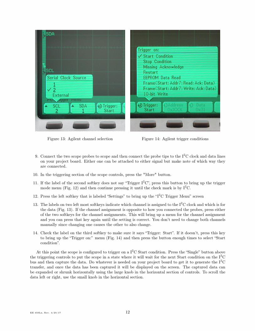
Figure 13: Agilent channel selection Figure 14: Agilent trigger conditions
9. Connect the two scope probes to scope and then connect the probe tips to the I2C clock and data lineson your project board. Either one can be attached to either signal but make note of which way theyare connected.
10. In the triggering section of the scope controls, press the "More" button.
11. If the label of the second softkey does not say “Trigger I2C”, press this button to bring up the triggermode menu (Fig. 12) and then continue pressing it until the check mark is by I2C.
12. Press the left softkey that is labeled “Settings” to bring up the “I2C Trigger Menu” screen
13. The labels on two left most softkeys indicate which channel is assigned to the I2C clock and which is forthe data (Fig. 13). If the channel assignment is opposite to how you connected the probes, press eitherof the two softkeys for the channel assignments. This will bring up a menu for the channel assignmentand you can press that key again until the setting is correct. You don’t need to change both channelsmanually since changing one causes the other to also change.
14. Check the label on the third softkey to make sure it says “Trigger: Start”. If it doesn’t, press this keyto bring up the “Trigger on:” menu (Fig. 14) and then press the button enough times to select “Startcondition”.
At this point the scope is configured to trigger on a I2C Start condition. Press the “Single” button abovethe triggering controls to put the scope in a state where it will wait for the next Start condition on the I2Cbus and then capture the data. Do whatever is needed on your project board to get it to generate the I2Ctransfer, and once the data has been captured it will be displayed on the screen. The captured data canbe expanded or shrunk horizontally using the large knob in the horizontal section of controls. To scroll thedata left or right, use the small knob in the horizontal section.
EE 459Lx, Rev. 4/20/17 12