mie resonance based all-dielectric metamaterials at...
TRANSCRIPT

Mie Resonance Based All-Dielectric Metamaterials at Optical Frequencies
By
Parikshit Moitra
Dissertation
Submitted to the Faculty of the
Graduate School of Vanderbilt University
in partial fulfillment of the requirements
for the degree of
DOCTOR OF PHILOSOPHY
in
Interdisciplinary Materials Science
August, 2015
Nashville, Tennessee
Approved:
Professor Jason G. Valentine
Professor Sharon M. Weiss
Professor Richard F. Haglund Jr.
Professor Norman H. Tolk
Professor Deyu Li

Copyright @ 2015 by Parikshit Moitra
All Rights Reserved

iii
To my beloved parents and siblings
For their never ending support and motivation

iv
Acknowledgement
I take this opportunity to acknowledge the contribution of my professors, co-workers,
friends and family for their love, support and guidance throughout my doctoral studies. Without
their support the journey to completion of my PhD would not have been possible.
First and foremost, I would like to thank my PhD advisor Professor Jason Valentine for
giving me the opportunity to work with him in his newly formed lab in the Summer of 2009 and
introducing me to the wonder-world of metamaterials. I learned a lot from him in every aspect of
research, be it numerical modeling, fabrication or experiment. I acknowledge the excellent
guidance and support he provided me throughout my graduate studies.
I would also like to thank PhD committee members Prof Sharon Weiss, Prof Richard
Haglund, Prof Norman Tolk and Prof Deyu Li. They not only did an excellent job in evaluating
and critiquing my research, also taught me courses in Physics and Optoelectronics and let me
work in their labs as Research Rotation student.
A special thanks is given to all my lab members in Valentine Lab - Wenyi Wang,
Yuanmu Yang, Wei Li, Zack Coppens and Zhihua Zhu, who have been thoroughly helpful and
cooperative and they made working in the lab so much fun. Thanks for all the memories.
My acknowledgement won’t be complete if I do not mention the staff scientists in
Vanderbilt Institute of Nanoscale Science and Engineering (VINSE) and Center for Nanophase
Materials Sciences (CNMS), especially Dr. Ivan Kravchencko, Dayrl Briggs, Prof Anthony
Hmelo and Dr. Benjamin Schmidt, for training me on nanofabrication tools and helping me out
whenever I stumbled with any fabrication problems. I would also like to thank my collaborators,
especially Dr. Brian Slovick and Dr. Srini Krishnamurthy in SRI International, for their
theoretical inputs in my research.

v
A special thanks goes to my maternal grandfather Dr. Shankar Nath Mukherjee for
motivating me to take graduate studies in the first place.
Finally and most importantly, I would like to thank my parents (Maa and Baba), my
brother Parashar Moitra and my sister Pallabi Moitra, for their unconditional love and support.
Thank you for believing in me.
vi
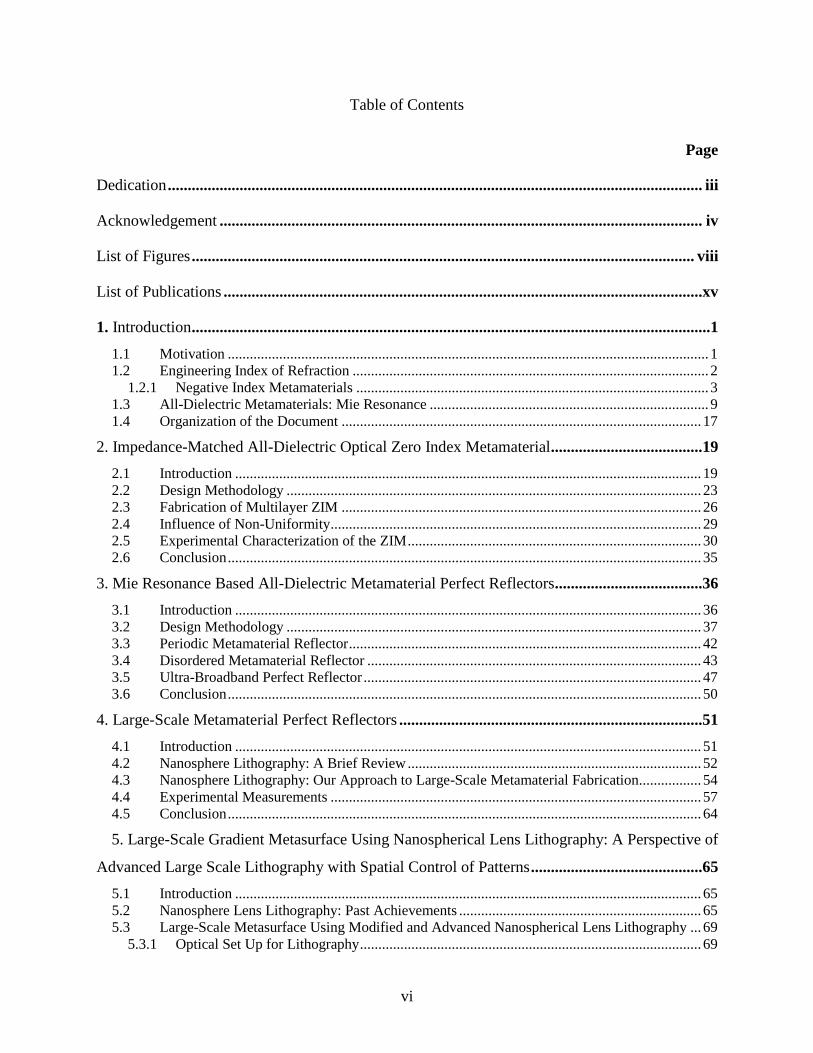
Table of Contents
Page
Dedication ...................................................................................................................................... iii
Acknowledgement ......................................................................................................................... iv
List of Figures .............................................................................................................................. viii
List of Publications ........................................................................................................................xv
1. Introduction ..................................................................................................................................1
1.1 Motivation ................................................................................................................................... 1 1.2 Engineering Index of Refraction ................................................................................................. 2
1.2.1 Negative Index Metamaterials ................................................................................................ 3 1.3 All-Dielectric Metamaterials: Mie Resonance ............................................................................ 9 1.4 Organization of the Document .................................................................................................. 17
2. Impedance-Matched All-Dielectric Optical Zero Index Metamaterial......................................19
2.1 Introduction ............................................................................................................................... 19 2.2 Design Methodology ................................................................................................................. 23 2.3 Fabrication of Multilayer ZIM .................................................................................................. 26 2.4 Influence of Non-Uniformity ..................................................................................................... 29 2.5 Experimental Characterization of the ZIM ................................................................................ 30 2.6 Conclusion ................................................................................................................................. 35
3. Mie Resonance Based All-Dielectric Metamaterial Perfect Reflectors.....................................36
3.1 Introduction ............................................................................................................................... 36 3.2 Design Methodology ................................................................................................................. 37 3.3 Periodic Metamaterial Reflector ................................................................................................ 42 3.4 Disordered Metamaterial Reflector ........................................................................................... 43 3.5 Ultra-Broadband Perfect Reflector ............................................................................................ 47 3.6 Conclusion ................................................................................................................................. 50
4. Large-Scale Metamaterial Perfect Reflectors ............................................................................51
4.1 Introduction ............................................................................................................................... 51 4.2 Nanosphere Lithography: A Brief Review ................................................................................ 52 4.3 Nanosphere Lithography: Our Approach to Large-Scale Metamaterial Fabrication ................. 54 4.4 Experimental Measurements ..................................................................................................... 57 4.5 Conclusion ................................................................................................................................. 64
5. Large-Scale Gradient Metasurface Using Nanospherical Lens Lithography: A Perspective of
Advanced Large Scale Lithography with Spatial Control of Patterns ...........................................65
5.1 Introduction ............................................................................................................................... 65 5.2 Nanosphere Lens Lithography: Past Achievements .................................................................. 65 5.3 Large-Scale Metasurface Using Modified and Advanced Nanospherical Lens Lithography ... 69
5.3.1 Optical Set Up for Lithography ............................................................................................. 69
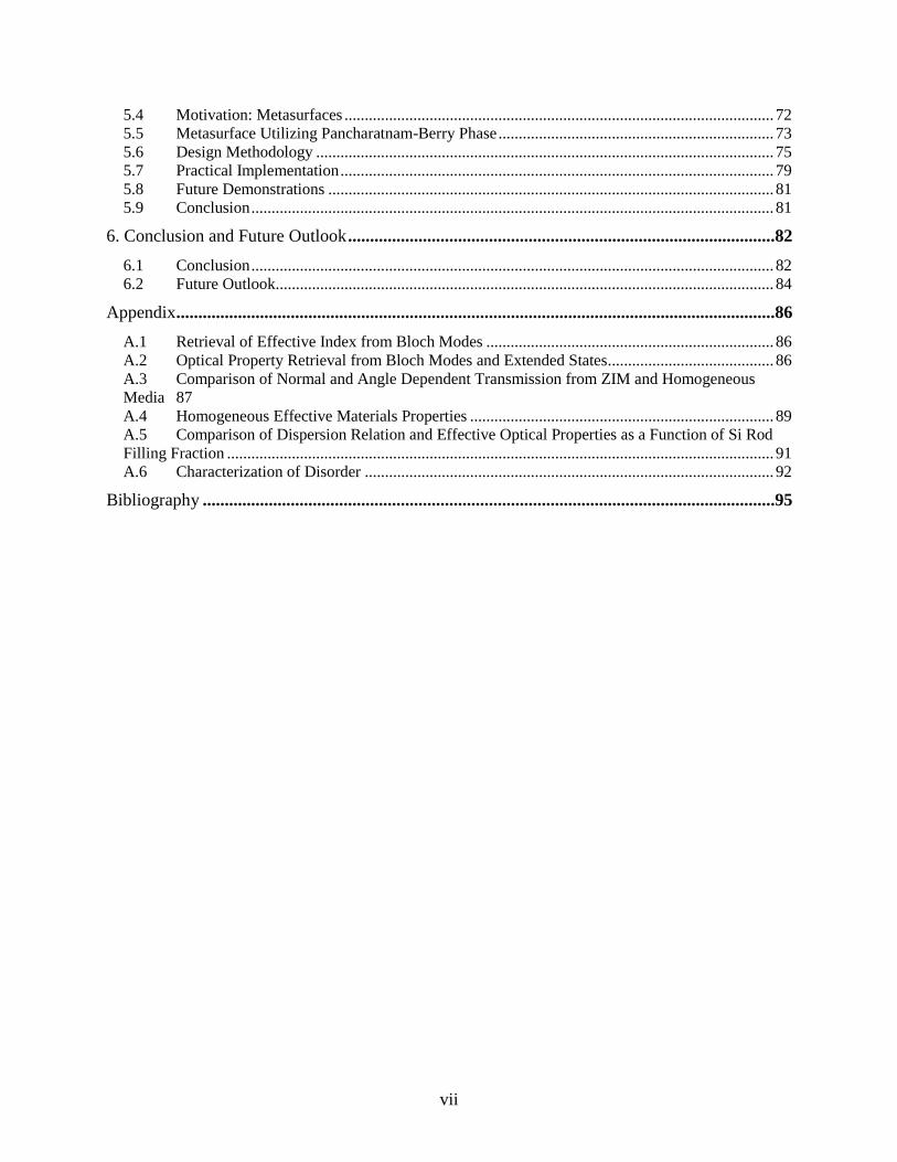
vii
5.4 Motivation: Metasurfaces .......................................................................................................... 72 5.5 Metasurface Utilizing Pancharatnam-Berry Phase .................................................................... 73 5.6 Design Methodology ................................................................................................................. 75 5.7 Practical Implementation ........................................................................................................... 79 5.8 Future Demonstrations .............................................................................................................. 81 5.9 Conclusion ................................................................................................................................. 81
6. Conclusion and Future Outlook .................................................................................................82
6.1 Conclusion ................................................................................................................................. 82 6.2 Future Outlook ........................................................................................................................... 84
Appendix ........................................................................................................................................86
A.1 Retrieval of Effective Index from Bloch Modes ....................................................................... 86 A.2 Optical Property Retrieval from Bloch Modes and Extended States ......................................... 86 A.3 Comparison of Normal and Angle Dependent Transmission from ZIM and Homogeneous
Media 87 A.4 Homogeneous Effective Materials Properties ........................................................................... 89 A.5 Comparison of Dispersion Relation and Effective Optical Properties as a Function of Si Rod
Filling Fraction ....................................................................................................................................... 91 A.6 Characterization of Disorder ..................................................................................................... 92
Bibliography ..................................................................................................................................95
viii
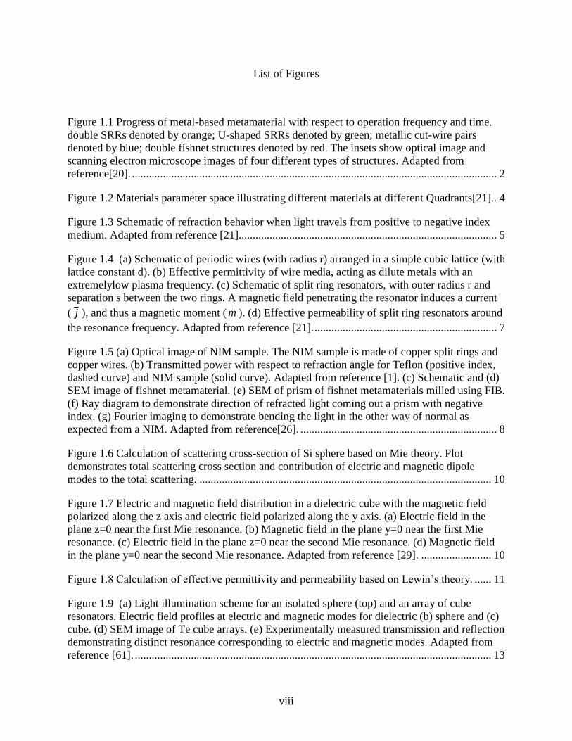
List of Figures
Figure 1.1 Progress of metal-based metamaterial with respect to operation frequency and time.
double SRRs denoted by orange; U-shaped SRRs denoted by green; metallic cut-wire pairs
denoted by blue; double fishnet structures denoted by red. The insets show optical image and
scanning electron microscope images of four different types of structures. Adapted from
reference[20]. .................................................................................................................................. 2
Figure 1.2 Materials parameter space illustrating different materials at different Quadrants[21]. . 4
Figure 1.3 Schematic of refraction behavior when light travels from positive to negative index
medium. Adapted from reference [21]. ........................................................................................... 5
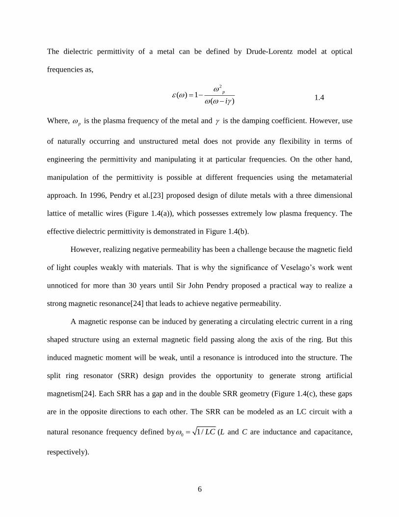
Figure 1.4 (a) Schematic of periodic wires (with radius r) arranged in a simple cubic lattice (with
lattice constant d). (b) Effective permittivity of wire media, acting as dilute metals with an
extremelylow plasma frequency. (c) Schematic of split ring resonators, with outer radius r and
separation s between the two rings. A magnetic field penetrating the resonator induces a current
( j ), and thus a magnetic moment ( m ). (d) Effective permeability of split ring resonators around
the resonance frequency. Adapted from reference [21]. ................................................................. 7
Figure 1.5 (a) Optical image of NIM sample. The NIM sample is made of copper split rings and
copper wires. (b) Transmitted power with respect to refraction angle for Teflon (positive index,
dashed curve) and NIM sample (solid curve). Adapted from reference [1]. (c) Schematic and (d)
SEM image of fishnet metamaterial. (e) SEM of prism of fishnet metamaterials milled using FIB.
(f) Ray diagram to demonstrate direction of refracted light coming out a prism with negative
index. (g) Fourier imaging to demonstrate bending the light in the other way of normal as
expected from a NIM. Adapted from reference[26]. ...................................................................... 8
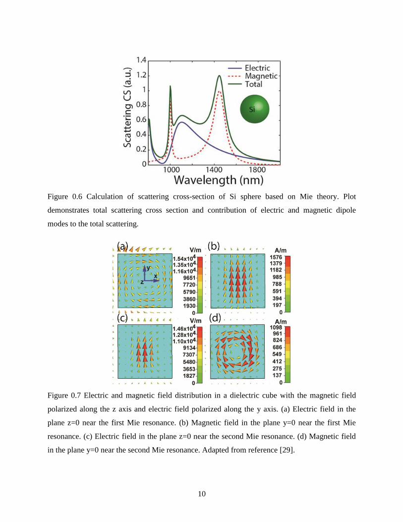
Figure 1.6 Calculation of scattering cross-section of Si sphere based on Mie theory. Plot
demonstrates total scattering cross section and contribution of electric and magnetic dipole
modes to the total scattering. ........................................................................................................ 10
Figure 1.7 Electric and magnetic field distribution in a dielectric cube with the magnetic field
polarized along the z axis and electric field polarized along the y axis. (a) Electric field in the
plane z=0 near the first Mie resonance. (b) Magnetic field in the plane y=0 near the first Mie
resonance. (c) Electric field in the plane z=0 near the second Mie resonance. (d) Magnetic field
in the plane y=0 near the second Mie resonance. Adapted from reference [29]. ......................... 10
Figure 1.8 Calculation of effective permittivity and permeability based on Lewin’s theory. ...... 11
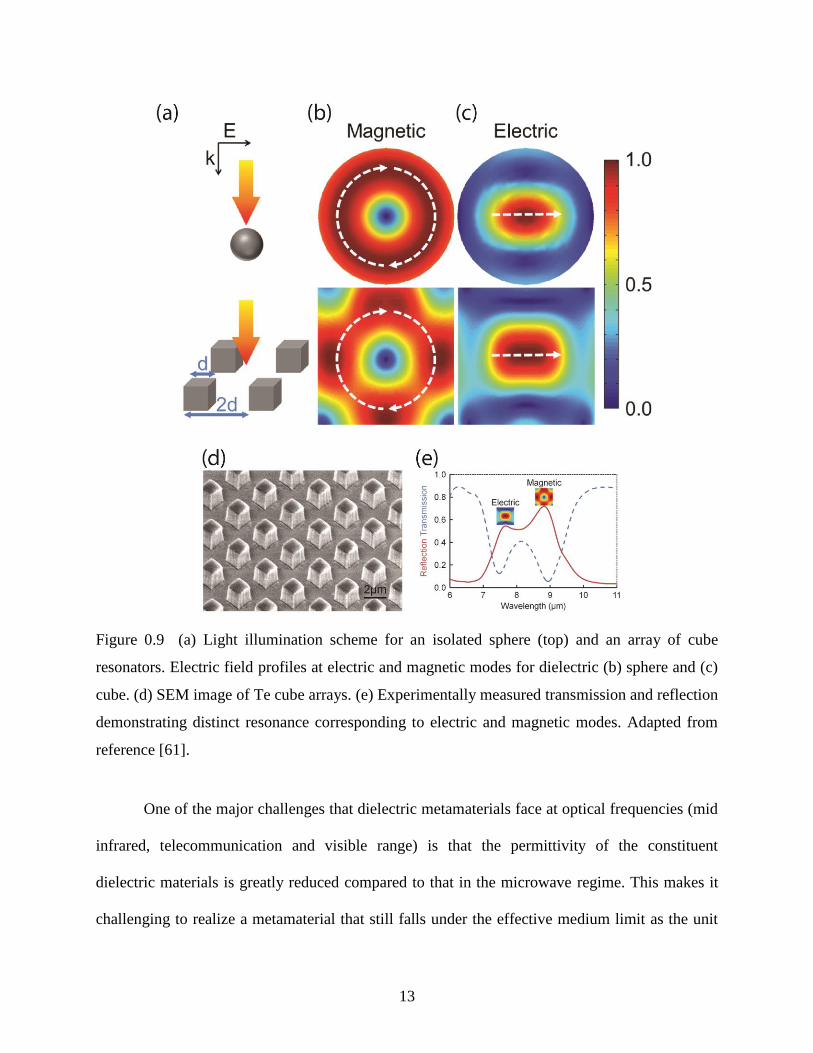
Figure 1.9 (a) Light illumination scheme for an isolated sphere (top) and an array of cube
resonators. Electric field profiles at electric and magnetic modes for dielectric (b) sphere and (c)
cube. (d) SEM image of Te cube arrays. (e) Experimentally measured transmission and reflection
demonstrating distinct resonance corresponding to electric and magnetic modes. Adapted from
reference [61]. ............................................................................................................................... 13
ix
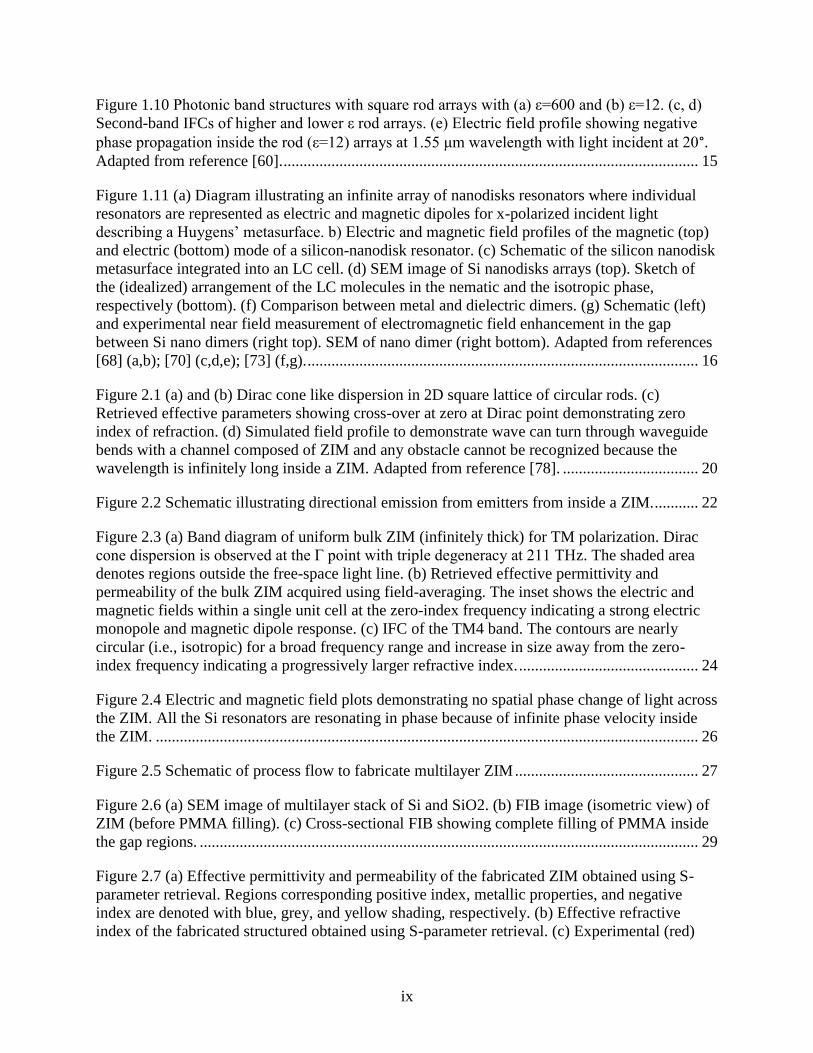
Figure 1.10 Photonic band structures with square rod arrays with (a) ε=600 and (b) ε=12. (c, d)
Second-band IFCs of higher and lower ε rod arrays. (e) Electric field profile showing negative
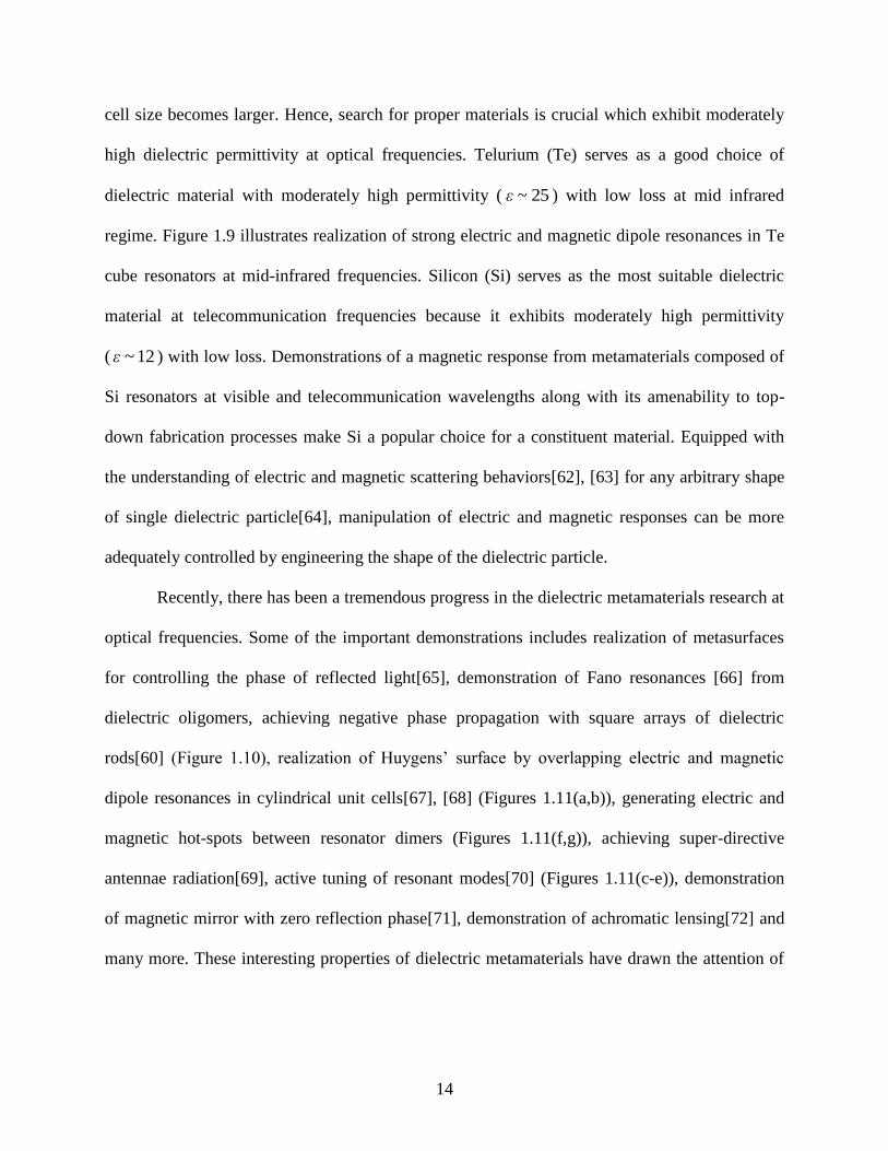
phase propagation inside the rod (ε=12) arrays at 1.55 μm wavelength with light incident at 20°. Adapted from reference [60]. ........................................................................................................ 15
Figure 1.11 (a) Diagram illustrating an infinite array of nanodisks resonators where individual
resonators are represented as electric and magnetic dipoles for x-polarized incident light
describing a Huygens’ metasurface. b) Electric and magnetic field profiles of the magnetic (top)
and electric (bottom) mode of a silicon-nanodisk resonator. (c) Schematic of the silicon nanodisk
metasurface integrated into an LC cell. (d) SEM image of Si nanodisks arrays (top). Sketch of
the (idealized) arrangement of the LC molecules in the nematic and the isotropic phase,
respectively (bottom). (f) Comparison between metal and dielectric dimers. (g) Schematic (left)
and experimental near field measurement of electromagnetic field enhancement in the gap
between Si nano dimers (right top). SEM of nano dimer (right bottom). Adapted from references
[68] (a,b); [70] (c,d,e); [73] (f,g). .................................................................................................. 16
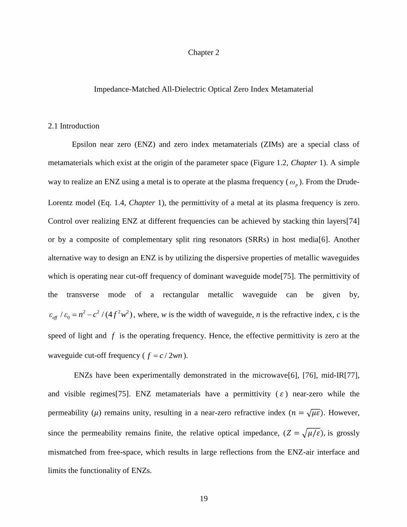
Figure 2.1 (a) and (b) Dirac cone like dispersion in 2D square lattice of circular rods. (c)
Retrieved effective parameters showing cross-over at zero at Dirac point demonstrating zero
index of refraction. (d) Simulated field profile to demonstrate wave can turn through waveguide
bends with a channel composed of ZIM and any obstacle cannot be recognized because the
wavelength is infinitely long inside a ZIM. Adapted from reference [78]. .................................. 20
Figure 2.2 Schematic illustrating directional emission from emitters from inside a ZIM. ........... 22
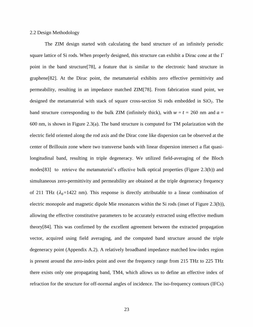
Figure 2.3 (a) Band diagram of uniform bulk ZIM (infinitely thick) for TM polarization. Dirac
cone dispersion is observed at the Γ point with triple degeneracy at 211 THz. The shaded area
denotes regions outside the free-space light line. (b) Retrieved effective permittivity and
permeability of the bulk ZIM acquired using field-averaging. The inset shows the electric and
magnetic fields within a single unit cell at the zero-index frequency indicating a strong electric
monopole and magnetic dipole response. (c) IFC of the TM4 band. The contours are nearly
circular (i.e., isotropic) for a broad frequency range and increase in size away from the zero-
index frequency indicating a progressively larger refractive index. ............................................. 24
Figure 2.4 Electric and magnetic field plots demonstrating no spatial phase change of light across
the ZIM. All the Si resonators are resonating in phase because of infinite phase velocity inside
the ZIM. ........................................................................................................................................ 26
Figure 2.5 Schematic of process flow to fabricate multilayer ZIM .............................................. 27
Figure 2.6 (a) SEM image of multilayer stack of Si and SiO2. (b) FIB image (isometric view) of
ZIM (before PMMA filling). (c) Cross-sectional FIB showing complete filling of PMMA inside
the gap regions. ............................................................................................................................. 29
Figure 2.7 (a) Effective permittivity and permeability of the fabricated ZIM obtained using S-
parameter retrieval. Regions corresponding positive index, metallic properties, and negative
index are denoted with blue, grey, and yellow shading, respectively. (b) Effective refractive
index of the fabricated structured obtained using S-parameter retrieval. (c) Experimental (red)

x
and theoretical transmittance (dotted blue) curves of the ZIM (200 x 200 µm2
total pattern area).
....................................................................................................................................................... 30
Figure 2.8 (a) IFCs of air and a low-index metamaterial illustrating angularly selective
transmission due to conservation of the wave vector parallel to the surface. (b) Simulated angle
and wavelength-dependent transmittance of the fabricated structure. (c-f) Fourier-plane images
of a beam passing through the fabricated ZIM structure within the low index band. Angularly
selective transmission can be observed in the y-direction due to the low effective index. Along
the x-direction, angular selectivity is not preserved due to the one-dimensional nature of Si rods.
(g) Fourier-plane image of the illumination beam demonstrating uniform intensity over the
angular range measured. ............................................................................................................... 31
Figure 2.9 QD Emission Spectrum. Photoluminescence (PL) spectrum of PbS quantum dots
(Evident Technology) used in the main text. The emission peak appears at 1425 nm, with a full-
width at half-maximum of 172 nm. The blue-, gray- and yellow-shaded region corresponds to
positive index, metallic properties, and negative index as acquired from S-parameter retrieval.
The dip of measured luminescence spectrum at around 1380 nm is due to the water absorption
line................................................................................................................................................. 33
Figure 2.10 (a) Schematic of laser-pumped QD emission from within the ZIM structure. (b)
Calculated emission profile for a line source placed in the center of the material (centered) and
the average profile from line sources placed throughout the material (averaged). (c) 2D Fourier-
plane images of quantum dot emission on the substrate, intensity is scaled by two times. (d) A
cross-section of the emission taken at kx = 0. (e) 2D Fourier-plane images of QD emission within
the ZIM, respectively, showing enhanced rate and directivity of spontaneous emission. (f) A
cross-section of the emission taken at kx = 0. ............................................................................... 34
Figure 3.1 (a) Scattering cross-sections of single Si (ε = 12) cylinder resonators embedded in an
air background for two different aspect ratios (AR = 1.25 and AR = 0.6). Solid and dashed lines
represent the electric and magnetic contributions to the scattering cross-section, respectively. (b)
Diagram showing incident plane wave polarization and the azimuthal angles of polar coordinates
for scattering cross section calculation (c) Polar plot of electric and magnetic contribution to
scattering cross sections (m2) at the respective Mie modes at θ = 90° plane with φ varying from 0°
to 360°. (d) Magnetic and electric field profiles at the center of single disk resonator at respective
dipole modes. ................................................................................................................................ 38
Figure 3.2 (a) Spectral positions of the electric and magnetic dipole Mie resonances as a function
of the AR. The solid lines are fitted to the points as a guide for the eye. (b) Simulated reflectance
plots for periodic Si cylinder metamaterials, illustrating reflectance as a function of cylinder AR.
....................................................................................................................................................... 40
Figure 3.3 (a) Effective permittivity and (b) permeability of a periodic cylinder resonator-based
metamaterial in an air background with a resonator geometry corresponding to D = 400 nm, H =
500 nm, and a periodicity of 660 nm. (c) Retrieved n and z for the periodic metamaterial. (d)
Reflectance of the metamaterial array numerically calculated using HFSS. A 100 nm near-
perfect reflectance band is achieved (reflectance > 99%) from 1398 to 1498 nm. ...................... 41
xi
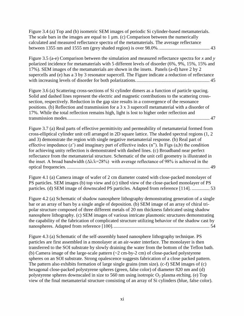
Figure 3.4 (a) Top and (b) isometric SEM images of periodic Si cylinder-based metamaterials.
The scale bars in the images are equal to 1 µm. (c) Comparison between the numerically
calculated and measured reflectance spectra of the metamaterials. The average reflectance
between 1355 nm and 1555 nm (grey shaded region) is over 98.0%. .......................................... 43
Figure 3.5 (a-e) Comparison between the simulation and measured reflectance spectra for x and y
polarized incidence for metamaterials with 5 different levels of disorder (6%, 9%, 15%, 15% and
17%). SEM images of the metamaterials are shown in the insets. Panels (a-d) have 2 by 2
supercells and (e) has a 3 by 3 resonator supercell. The Figure indicate a reduction of reflectance
with increasing levels of disorder for both polarizations. ............................................................. 45
Figure 3.6 (a) Scattering cross-sections of Si cylinder dimers as a function of particle spacing.
Solid and dashed lines represent the electric and magnetic contributions to the scattering cross-
section, respectively. Reduction in the gap size results in a convergence of the resonance
positions. (b) Reflection and transmission for a 3 x 3 supercell metamaterial with a disorder of
17%. While the total reflection remains high, light is lost to higher order reflection and
transmission modes. ...................................................................................................................... 47
Figure 3.7 (a) Real parts of effective permittivity and permeability of metamaterial formed from
cross-elliptical cylinder unit cell arranged in 2D square lattice. The shaded spectral regions (1, 2
and 3) demonstrate the region with single negative metamaterial response. (b) Real part of
effective impedance (z’) and imaginary part of effective index (n”). In Figs (a,b) the condition
for achieving unity reflection is demonstrated with dashed lines. (c) Broadband near perfect
reflectance from the metamaterial structure. Schematic of the unit cell geometry is illustrated in
the inset. A broad bandwidth (Δλ/λ=28%) with average reflectance of 98% is achieved in the
optical frequencies. ....................................................................................................................... 49
Figure 4.1 (a) Camera image of wafer of 2 cm diameter coated with close-packed monolayer of
PS particles. SEM images (b) top view and (c) tilted view of the close-packed monolayer of PS
particles. (d) SEM image of downscaled PS particles. Adapted from reference [114]. ............... 53
Figure 4.2 (a) Schematic of shadow nanosphere lithography demonstrating generation of a single
bar or an array of bars by a single angle of deposition. (b) SEM image of an array of chiral tri-
polar structure composed of three different metals of 20 nm thickness fabricated using shadow
nanosphere lithography. (c) SEM images of various intricate plasmonic structures demonstrating
the capability of the fabrication of complicated structure utilizing behavior of the shadow cast by
nanospheres. Adapted from reference [100]. ................................................................................ 54
Figure 4.3 (a) Schematic of the self-assembly based nanosphere lithography technique. PS
particles are first assembled in a monolayer at an air-water interface. The monolayer is then
transferred to the SOI substrate by slowly draining the water from the bottom of the Teflon bath.
(b) Camera image of the large-scale pattern (~2 cm-by-2 cm) of close-packed polystyrene
spheres on an SOI substrate. Strong opalescence suggests fabrication of a close packed pattern.
The pattern also exhibits formation of large single grains (mm size). (c-f) SEM images of (c)
hexagonal close-packed polystyrene spheres (green, false color) of diameter 820 nm and (d)
polystyrene spheres downscaled in size to 560 nm using isotropic O2 plasma etching. (e) Top
view of the final metamaterial structure consisting of an array of Si cylinders (blue, false color).
xii
The cylinders were formed by using SF6/ C4F8 reactive ion etch chemistry. (f) Tilted view (45°) of the final metamaterial consisting of an array of Si cylinders (blue, false color). The inset
shows an SEM image of a single Si resonator with a top diameter (Dtop), bottom diameter (Dbottom)
and height (H) of 480 nm, 554 nm and 335 nm, respectively. The scale bar for SEM images (c-f)
is 2 μm. .......................................................................................................................................... 57
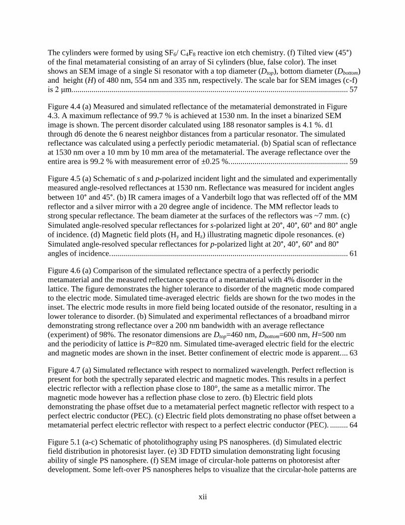
Figure 4.4 (a) Measured and simulated reflectance of the metamaterial demonstrated in Figure
4.3. A maximum reflectance of 99.7 % is achieved at 1530 nm. In the inset a binarized SEM
image is shown. The percent disorder calculated using 188 resonator samples is 4.1 %. d1
through d6 denote the 6 nearest neighbor distances from a particular resonator. The simulated
reflectance was calculated using a perfectly periodic metamaterial. (b) Spatial scan of reflectance
at 1530 nm over a 10 mm by 10 mm area of the metamaterial. The average reflectance over the
entire area is 99.2 % with measurement error of ±0.25 %. ........................................................... 59
Figure 4.5 (a) Schematic of s and p-polarized incident light and the simulated and experimentally
measured angle-resolved reflectances at 1530 nm. Reflectance was measured for incident angles
between 10° and 45°. (b) IR camera images of a Vanderbilt logo that was reflected off of the MM
reflector and a silver mirror with a 20 degree angle of incidence. The MM reflector leads to
strong specular reflectance. The beam diameter at the surfaces of the reflectors was ~7 mm. (c)
Simulated angle-resolved specular reflectances for s-polarized light at 20°, 40°, 60° and 80° angle
of incidence. (d) Magnetic field plots (Hy and Hz) illustrating magnetic dipole resonances. (e)
Simulated angle-resolved specular reflectances for p-polarized light at 20°, 40°, 60° and 80° angles of incidence. ....................................................................................................................... 61
Figure 4.6 (a) Comparison of the simulated reflectance spectra of a perfectly periodic
metamaterial and the measured reflectance spectra of a metamaterial with 4% disorder in the
lattice. The figure demonstrates the higher tolerance to disorder of the magnetic mode compared
to the electric mode. Simulated time-averaged electric fields are shown for the two modes in the
inset. The electric mode results in more field being located outside of the resonator, resulting in a
lower tolerance to disorder. (b) Simulated and experimental reflectances of a broadband mirror
demonstrating strong reflectance over a 200 nm bandwidth with an average reflectance
(experiment) of 98%. The resonator dimensions are Dtop=460 nm, Dbottom=600 nm, H=500 nm
and the periodicity of lattice is P=820 nm. Simulated time-averaged electric field for the electric
and magnetic modes are shown in the inset. Better confinement of electric mode is apparent. ... 63
Figure 4.7 (a) Simulated reflectance with respect to normalized wavelength. Perfect reflection is
present for both the spectrally separated electric and magnetic modes. This results in a perfect
electric reflector with a reflection phase close to 180°, the same as a metallic mirror. The
magnetic mode however has a reflection phase close to zero. (b) Electric field plots
demonstrating the phase offset due to a metamaterial perfect magnetic reflector with respect to a
perfect electric conductor (PEC). (c) Electric field plots demonstrating no phase offset between a
metamaterial perfect electric reflector with respect to a perfect electric conductor (PEC). ......... 64
Figure 5.1 (a-c) Schematic of photolithography using PS nanospheres. (d) Simulated electric
field distribution in photoresist layer. (e) 3D FDTD simulation demonstrating light focusing
ability of single PS nanosphere. (f) SEM image of circular-hole patterns on photoresist after
development. Some left-over PS nanospheres helps to visualize that the circular-hole patterns are
xiii
transferred from the nanospheres. (g) Cross-sectional view of circular-hole patterns in photoresist.
Adapted from references [119] (a-d), [120] (e-g). ........................................................................ 66
Figure 5.2 (a-c) Simulated electric field demonstrating field concentration in elliptical spatial
pattern as asymmetric UV light focused by PS nanosphere. Adapted from reference [118]. ..... 67
Figure 5.3 SEM images at different steps of lithography to generate elliptical patterns. (a) Self-
assembled close-packed nanospheres. (b) Elliptical-hole patterns in photoresist after lift-off. (c,d)
metal nanorods after lift-off, oriented differently. Adapted from reference [118]. ...................... 69
Figure 5.4 (a) Schematic of the optical set-up for gradient patterning using nanosphere lens
lithography. (b) Schematic of spatial light pattern. (c) Fourier plane masking to achieve elliptical
hole patterns oriented differently. ................................................................................................. 71
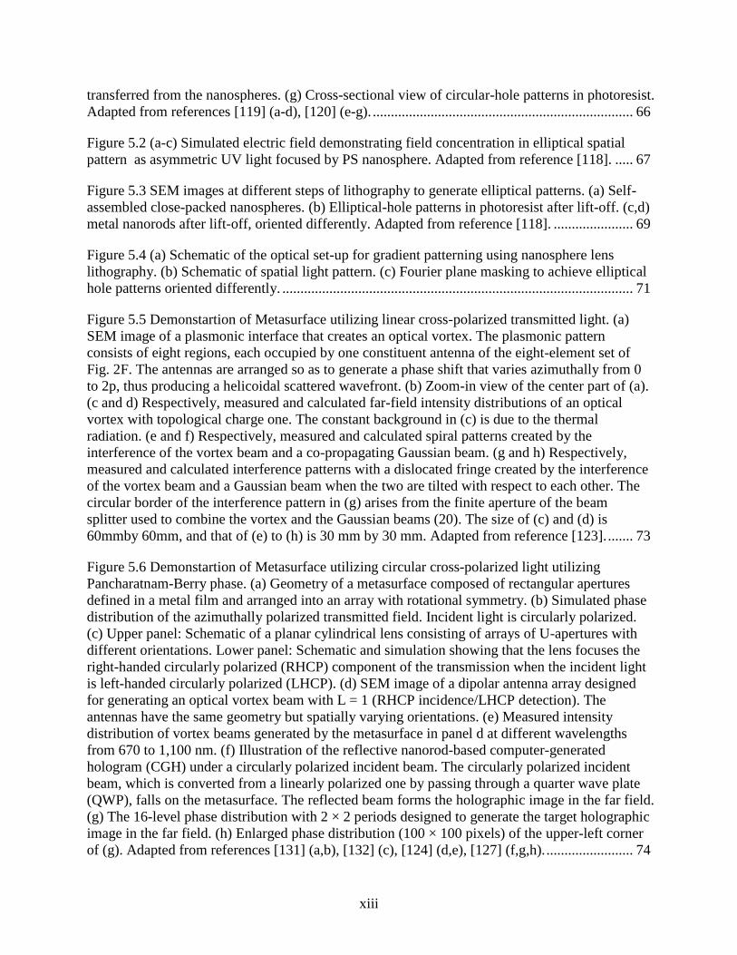
Figure 5.5 Demonstartion of Metasurface utilizing linear cross-polarized transmitted light. (a)
SEM image of a plasmonic interface that creates an optical vortex. The plasmonic pattern
consists of eight regions, each occupied by one constituent antenna of the eight-element set of
Fig. 2F. The antennas are arranged so as to generate a phase shift that varies azimuthally from 0
to 2p, thus producing a helicoidal scattered wavefront. (b) Zoom-in view of the center part of (a).
(c and d) Respectively, measured and calculated far-field intensity distributions of an optical
vortex with topological charge one. The constant background in (c) is due to the thermal
radiation. (e and f) Respectively, measured and calculated spiral patterns created by the
interference of the vortex beam and a co-propagating Gaussian beam. (g and h) Respectively,
measured and calculated interference patterns with a dislocated fringe created by the interference
of the vortex beam and a Gaussian beam when the two are tilted with respect to each other. The
circular border of the interference pattern in (g) arises from the finite aperture of the beam
splitter used to combine the vortex and the Gaussian beams (20). The size of (c) and (d) is
60mmby 60mm, and that of (e) to (h) is 30 mm by 30 mm. Adapted from reference [123]. ....... 73
Figure 5.6 Demonstartion of Metasurface utilizing circular cross-polarized light utilizing
Pancharatnam-Berry phase. (a) Geometry of a metasurface composed of rectangular apertures
defined in a metal film and arranged into an array with rotational symmetry. (b) Simulated phase
distribution of the azimuthally polarized transmitted field. Incident light is circularly polarized.
(c) Upper panel: Schematic of a planar cylindrical lens consisting of arrays of U-apertures with
different orientations. Lower panel: Schematic and simulation showing that the lens focuses the
right-handed circularly polarized (RHCP) component of the transmission when the incident light
is left-handed circularly polarized (LHCP). (d) SEM image of a dipolar antenna array designed
for generating an optical vortex beam with L = 1 (RHCP incidence/LHCP detection). The
antennas have the same geometry but spatially varying orientations. (e) Measured intensity
distribution of vortex beams generated by the metasurface in panel d at different wavelengths
from 670 to 1,100 nm. (f) Illustration of the reflective nanorod-based computer-generated
hologram (CGH) under a circularly polarized incident beam. The circularly polarized incident
beam, which is converted from a linearly polarized one by passing through a quarter wave plate
(QWP), falls on the metasurface. The reflected beam forms the holographic image in the far field.
(g) The 16-level phase distribution with 2 × 2 periods designed to generate the target holographic
image in the far field. (h) Enlarged phase distribution (100 × 100 pixels) of the upper-left corner
of (g). Adapted from references [131] (a,b), [132] (c), [124] (d,e), [127] (f,g,h). ........................ 74

xiv
Figure 5.7 (a) Reflectances from an array of elliptical cylinder resonators with electric field
polarized along long and short axes, respectively. (b) Reflection phase plot demonstrating π
phase difference between reflections from two linear polarizations for 200 nm broad bandwidth.
....................................................................................................................................................... 76
Figure 5.8 (a) Schematic of elliptical patterns with different orientations. (b) Broadband cross-
polarized reflectance as a function of orientation of resonators. (c) Broadband cross-polarized
reflection phase as a function of orientation of resonators. Complete phase control from 0 to 2π is
demonstrated for over 200 nm bandwidth. (d,e) Phase profiles for optical vortex generator and
axicon, respectively....................................................................................................................... 78
Figure 5.9 Schematic of fabrication process flow. ....................................................................... 80
xv
List of Publications
Peer Reviewed
Parikshit Moitra, Yuanmu Yang, Zachary Anderson, Ivan I. Kravchencko, Daryl P.
Briggs & Jason Valentine. Realization of an all-dielectric zero-index optical metamaterial.
Nature Photonics 7, 791–795 (2013).
Parikshit Moitra, Brian Slovick, Zhi Gang Yu, Srini Krishnamurthy & Jason Valentine.
Experimental demonstration of a broadband all-dielectric metamaterial perfect reflector.
Applied Physics Letters 104, 171102 (2014).
Parikshit Moitra, Brian Slovick, Wei Li, Ivan I. Kravchencko, Daryl P. Briggs, Srini
Krishnamurthy & Jason Valentine. Large scale all-dielectric metamaterial perfect
reflectors. ACS Photonics 2, 692-698 (2015)
Yuanmu Yang, Wenyi Wang, Parikshit Moitra, Ivan I. Kravchencko, Daryl P. Briggs &
Jason Valentine. Dielectric meta-reflectarray for broadband linear polarization
conversion and optical vortex generation. Nano Letters 14, 1394-1399 (2014).
Aditya Jain, Parikshit Moitra, Thomas Koschny, Jason Valentine & Costas M.
Soukoulis. Electric and magnetic response in dielectric dark states for low loss
subwavelength optical meta atoms. Accepted in Advanced Optical Materials (2015)
1
Chapter 1
Introduction
1.1 Motivation
Electromagnetic metamaterials are artificially fabricated structures that exhibit properties
unattainable in naturally occurring materials, such as negative index[1]–[4], epsilon-near-
zero[5]–[7], ultra-high index[8], perfect lensing[9], [10] and cloaking[4], [11]–[13]. Since their
inception, metallic unit cells have dominated the field of metamaterials. However, metallic unit
cells suffer from conduction loss[14]–[16], magnetic saturation at high frequencies[17], exhibit
anisotropic optical responses[18] and requires expensive lithography method for fabrication and
hence large area scalability is not feasible for practical applications. Recently, there has been
burgeoning interest in exploiting the Mie resonances[19] in dielectric particles with simple
geometries to design all-dielectric metamaterials, which not only have much less absorption
losses at optical frequencies than their metallic counterparts, but also provide the potential for
achieving isotropic optical responses by simplifying the design. The main motivations of this
dissertation are two fold - first, to understand how electric and magnetic Mie resonances in
dielectric particles can be used to design metamaterials exhibiting novel and unique optical
properties; and second, to experimentally realize metamaterials using nanofabrication techniques,
with a strong motivation towards scaling the metamaterial to large area for practical applications.
This chapter will serve as a guide to understand the inception and brief history of metallic
metamaterials and will also help us to understand the limitations of metallic unit cells and
advantages of transition from metallic unit cells to their dielectric counterparts.
2
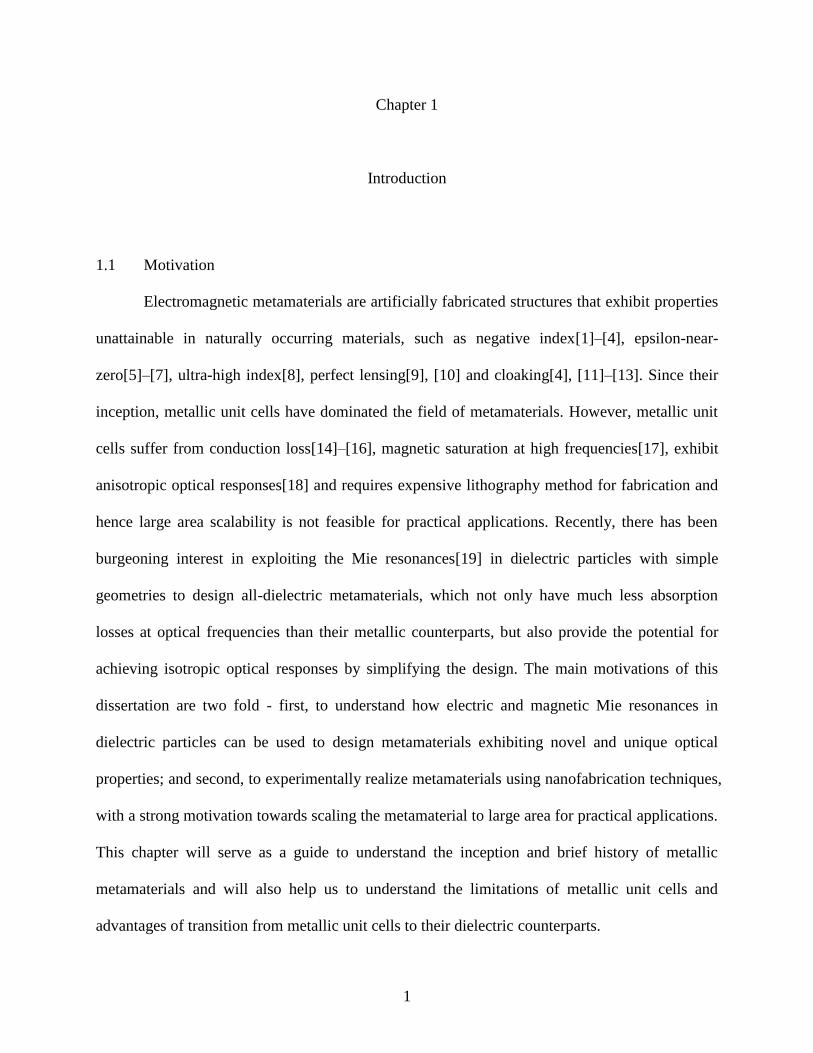
Figure 0.1 Progress of metal-based metamaterial with respect to operation frequency and time.
double SRRs denoted by orange; U-shaped SRRs denoted by green; metallic cut-wire pairs
denoted by blue; double fishnet structures denoted by red. The insets show optical image and
scanning electron microscope images of four different types of structures. Adapted from
reference[20].
1.2 Engineering Index of Refraction
The field of metamaterials provides the framework to engineer optical properties, which
would not otherwise be possible using naturally occurring materials. To achieve novel optical
properties metamaterials needs to be artificially fabricated with periodic or random arrays of
properly structured elements or unit cells, the size and spacing of which must be much smaller
than the wavelength of electromagnetic radiation. Hence, the probing wavelength cannot “see”
individual unit cells and the collective response from all the unit cells can be modeled using a
homogeneous effective permittivity and permeability. Most interesting of all is that the effective
permeability can also be controlled by proper unit cell design.
3
1.2.1 Negative Index Metamaterials
It is useful to begin the discussion of metamaterials with negative index of refraction to
comprehend the inception of this field and how it excited the imagination of researchers
worldwide. Refractive index is a complex number given by n n n . n is a measure of how
the phase velocity of light is slowed down when passing through a material and n is a measure
of absorption of electromagnetic radiation and hence loss. The complex refractive index is
defined by n , where and are the complex electric permittivity and magnetic
permeability of a material. ε and μ define the polarizabilities of a material under the electric and
magnetic field of light, respectively. Based on their ε and μ values all the materials can be
categorized in terms of materials parameter space[21]. The materials parameter space is divided
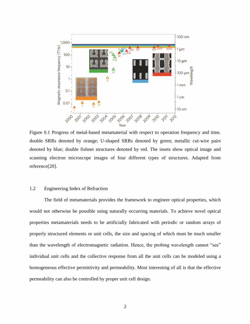
in four quadrants (Figure 1.2). Quadrant I lists most of the dielectric materials with simultaneous
positive permittivity and permeability. Quadrant II consists of materials with negative
permittivity such as metals and doped semiconductors. Quadrant IV consists of materials with
negative permeability but positive permittivity, which includes some ferrite materials. The most
interesting region is Quadrant III with simultaneous negative permittivity and permeability. No
naturally occurring materials belong to this region of parameter space.
Veselago[22] in 1968 was the first to postulate the optical properties of a hypothetical
material exhibiting simultaneous negative values of permittivity and permeability i.e. negative
index of refraction. He postulated that when light propagates from a positive index to negative
index material, or vice versa, it will refract in the wrong way i.e. at the same side of the normal
to the interface. To understand this concept let us review Maxwell’s equations (Eq. 1.1) and the
constitutive equations (Eq. 1.2), where the electric and magnetic fields of incident plane wave
are defined as 0( , ) exp( . . )E ω k E ik r iω t and 0( , ) exp( . . )H ω k H ik r iω t , respectively.

4
Figure 0.2 Materials parameter space illustrating different materials at different Quadrants[21].
0,
,
,
,
B
BE
t
D
DH j
t
0
0
r
r
D E E
B H H
Here, B is the magnetic flux density, D is the electric flux density, is the charge density, and j is
the current density. In absence of any free charges ( ρ ) and currents ( j ), Eq. 1.1 and 1.2 can be
1.1
1.2
5
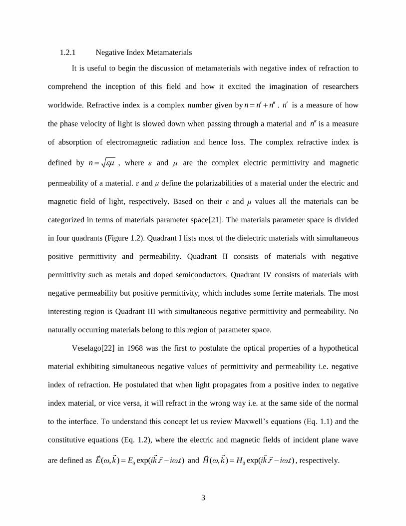
simplified to
k E μωH
k H εωE
For the propagation of a plane wave in conventional dielectric materials with 0ε and 0μ ,
the triplet vectors, k , E and H , follow the right hand rule (Eq. 1.3). However, during
propagation in a medium with 0ε and 0μ , these vectors follow the left-hand rule. Contrary
to conventional understanding, the Poynting vector, which is defined as S E H , and the wave
vector k are directed in opposite directions in such media (Figure 1.3). Furthermore, the real
part of refractive index which is given by r rn ε μ , should take a negative sign to conserve
causality[22].
Figure 0.3 Schematic of refraction behavior when light travels from positive to negative index
medium. Adapted from reference [21].
Designing Simultaneous Negative Permittivity and Permeability: Realization of negative
index requires both permittivity ( ) and permeability ( ) to be negative. Realizing negative
permittivity is relatively simple. Metals possess negative permittivity below plasma frequency.
1.3
6
The dielectric permittivity of a metal can be defined by Drude-Lorentz model at optical
frequencies as,
2
( ) 1( )
p
i
Where, p is the plasma frequency of the metal and is the damping coefficient. However, use
of naturally occurring and unstructured metal does not provide any flexibility in terms of
engineering the permittivity and manipulating it at particular frequencies. On the other hand,
manipulation of the permittivity is possible at different frequencies using the metamaterial
approach. In 1996, Pendry et al.[23] proposed design of dilute metals with a three dimensional
lattice of metallic wires (Figure 1.4(a)), which possesses extremely low plasma frequency. The
effective dielectric permittivity is demonstrated in Figure 1.4(b).
However, realizing negative permeability has been a challenge because the magnetic field
of light couples weakly with materials. That is why the significance of Veselago’s work went
unnoticed for more than 30 years until Sir John Pendry proposed a practical way to realize a
strong magnetic resonance[24] that leads to achieve negative permeability.
A magnetic response can be induced by generating a circulating electric current in a ring
shaped structure using an external magnetic field passing along the axis of the ring. But this
induced magnetic moment will be weak, until a resonance is introduced into the structure. The
split ring resonator (SRR) design provides the opportunity to generate strong artificial
magnetism[24]. Each SRR has a gap and in the double SRR geometry (Figure 1.4(c), these gaps
are in the opposite directions to each other. The SRR can be modeled as an LC circuit with a
natural resonance frequency defined by 0 1/ LC (L and C are inductance and capacitance,
respectively).
1.4
7
A strong circulating electric field can be induced in the SRR by magnetic flux directed
along the axis of the SRR in the frequency range centered at 0ω , which results in an effective
magnetic moment. The induced magnetic field can be either in or out of phase with the external
magnetic field. A strong induced magnetic field can lead to effective negative permeability.
Figure 0.4 (a) Schematic of periodic wires (with radius r) arranged in a simple cubic lattice (with
lattice constant d). (b) Effective permittivity of wire media, acting as dilute metals with an
extremelylow plasma frequency. (c) Schematic of split ring resonators, with outer radius r and
separation s between the two rings. A magnetic field penetrating the resonator induces a current
( j ), and thus a magnetic moment ( m ). (d) Effective permeability of split ring resonators around
the resonance frequency. Adapted from reference [21].
8
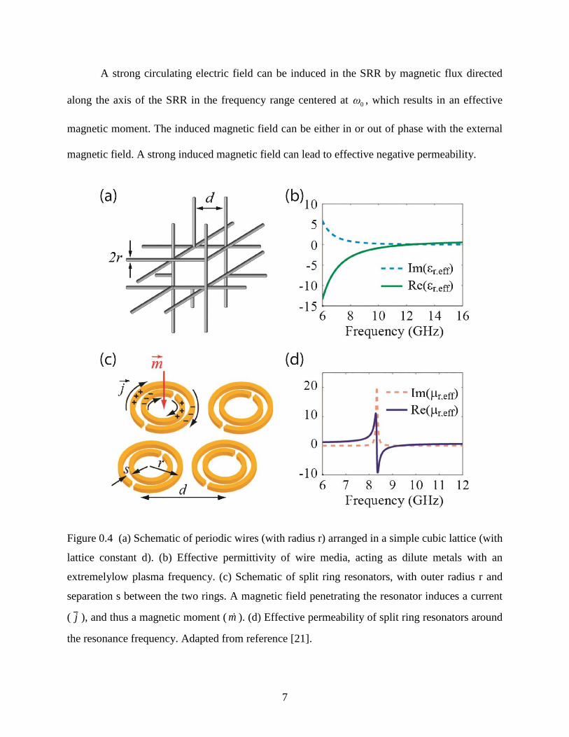
Figure 0.5 (a) Optical image of NIM sample. The NIM sample is made of copper split rings and
copper wires. (b) Transmitted power with respect to refraction angle for Teflon (positive index,
dashed curve) and NIM sample (solid curve). Adapted from reference [1]. (c) Schematic and (d)
SEM image of fishnet metamaterial. (e) SEM of prism of fishnet metamaterials milled using FIB.
(f) Ray diagram to demonstrate direction of refracted light coming out a prism with negative
index. (g) Fourier imaging to demonstrate bending the light in the other way of normal as
expected from a NIM. Adapted from reference[26].
Following Pendry’s work, Smith first experimentally demonstrated the practical
realization of a negative index medium [18] using periodic arrays of SRRs and a cut-wires
9
(Figure 1.5). All these ground breaking studies opened the door to the field of ‘metamaterials’
which has been followed by much work devoted to achieving better design methodologies for
negative index metamaterials at telecom (Figure 1.5) and visible frequencies[25]–[27].
1.3 All-Dielectric Metamaterials: Mie Resonance
Since the inception of metamaterials, researchers have strived to scale metamaterials to
optical frequencies[20], [28]. However, one of the major limitations in metal-based
metamaterials has been the presence of ohmic damping which results in absorption[14]–[16].
Moreover, as the plasmon resonance frequency is approached, the kinetic induction of the
electrons in the metal results in saturation of the magnetic response, limiting the use of metal-
based metamaterials at high frequencies[17]. In search for an alternative to metallic unit cells, the
interaction between electromagnetic waves and high dielectric materials has been investigated by
researchers. Exact theoretical solutions of light scattering by small dielectric spherical particles
was derived long ago by Lorentz and Mie and the theory is more popularly known as Mie theory
(Figure 1.6)[19].
Solutions to Mie theory for dielectric spherical particles yields electric and magnetic
multipole resonances characterized by peaks in the scattering coefficients. The lowest order
electric and magnetic resonances are the dipole modes. A magnetic dipole resonance is
accompanied by a circulating electric displacement current and an electric dipole resonance is
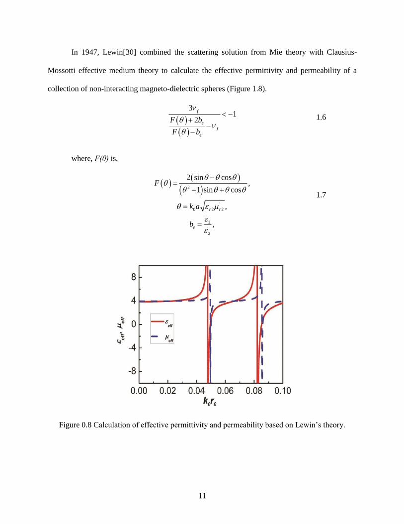
accompanied with a circulating magnetic field (Figure 1.7). These electric and magnetic dipole
resonances in a dielectric particle form the basis of utilizing them as a meta-atom.
10
Figure 0.6 Calculation of scattering cross-section of Si sphere based on Mie theory. Plot
demonstrates total scattering cross section and contribution of electric and magnetic dipole
modes to the total scattering.
Figure 0.7 Electric and magnetic field distribution in a dielectric cube with the magnetic field
polarized along the z axis and electric field polarized along the y axis. (a) Electric field in the
plane z=0 near the first Mie resonance. (b) Magnetic field in the plane y=0 near the first Mie
resonance. (c) Electric field in the plane z=0 near the second Mie resonance. (d) Magnetic field
in the plane y=0 near the second Mie resonance. Adapted from reference [29].
11
In 1947, Lewin[30] combined the scattering solution from Mie theory with Clausius-
Mossotti effective medium theory to calculate the effective permittivity and permeability of a
collection of non-interacting magneto-dielectric spheres (Figure 1.8).
31
2
f
e
f
e
F b
F b
where, F(θ) is,
2
' '
0 2 2
1
2
2 sin cos,
1 sin cos
,
,
r r
e
F
k a
b
Figure 0.8 Calculation of effective permittivity and permeability based on Lewin’s theory.
1.6
1.7
12
It didn’t take long to recognize the implications of Lewin’s work after the inception of
the field of metamaterials. In 2002, with a different approach than Lewin’s, O’Brien and
Pendry[31] showed that effective negative permeability can be obtained at the magnetic
resonance of ferroelectric rods arranged in a two dimensional lattice.
There are several advantages of using dielectric materials over metals as the metamaterial
building block. Firstly, dielectric materials experience less optical absorption than metals at high
frequencies, e.g. telecommunication and visible ranges. Secondly, dielectric materials do not
exhibit magnetic saturation at high frequencies. Thirdly, electric and magnetic Mie resonances
are inherent to dielectric particles with simple geometries opposed to more complicated metallic
unit cell geometries. The complicated unit cell geometry of metal based metamaterials leads to
anisotropic optical properties. Also, because of the complicated geometry of the metallic unit
cells, slow and expensive patterning techniques such as electron beam lithography or focused ion
beam lithography needs to be used to fabricate metal based metamaterials. This limits the
scalability of metal based metamaterials to large areas. However, due to having a simple unit cell
geometry, dielectric metamaterials are amenable low cost and high throughput patterning
techniques such as self-assembly based nanosphere lithography[32]–[49].
Dielectric metamaterial properties were first experimentally demonstrated in the
microwave regime[29], [50]–[54] which allows design of deep sub-wavelength unit cells because
of the availability of high dielectric constituents (e.g. ɛ > 100). Simple unit cell designs e.g
spheres[30], [55]–[58], cylinders[29], [31], [59], [60] and cubes[51]–[53], [61] have been used
to achieve all-dielectric metamaterials demonstrating high frequency magnetism[51]–[53], [59],
[61] and negative refractive index[29], [50], [54].
13
Figure 0.9 (a) Light illumination scheme for an isolated sphere (top) and an array of cube
resonators. Electric field profiles at electric and magnetic modes for dielectric (b) sphere and (c)
cube. (d) SEM image of Te cube arrays. (e) Experimentally measured transmission and reflection
demonstrating distinct resonance corresponding to electric and magnetic modes. Adapted from
reference [61].
One of the major challenges that dielectric metamaterials face at optical frequencies (mid
infrared, telecommunication and visible range) is that the permittivity of the constituent
dielectric materials is greatly reduced compared to that in the microwave regime. This makes it
challenging to realize a metamaterial that still falls under the effective medium limit as the unit
14
cell size becomes larger. Hence, search for proper materials is crucial which exhibit moderately
high dielectric permittivity at optical frequencies. Telurium (Te) serves as a good choice of
dielectric material with moderately high permittivity ( ~ 25ε ) with low loss at mid infrared
regime. Figure 1.9 illustrates realization of strong electric and magnetic dipole resonances in Te
cube resonators at mid-infrared frequencies. Silicon (Si) serves as the most suitable dielectric
material at telecommunication frequencies because it exhibits moderately high permittivity
( ~12ε ) with low loss. Demonstrations of a magnetic response from metamaterials composed of
Si resonators at visible and telecommunication wavelengths along with its amenability to top-
down fabrication processes make Si a popular choice for a constituent material. Equipped with
the understanding of electric and magnetic scattering behaviors[62], [63] for any arbitrary shape
of single dielectric particle[64], manipulation of electric and magnetic responses can be more
adequately controlled by engineering the shape of the dielectric particle.
Recently, there has been a tremendous progress in the dielectric metamaterials research at
optical frequencies. Some of the important demonstrations includes realization of metasurfaces
for controlling the phase of reflected light[65], demonstration of Fano resonances [66] from
dielectric oligomers, achieving negative phase propagation with square arrays of dielectric
rods[60] (Figure 1.10), realization of Huygens’ surface by overlapping electric and magnetic
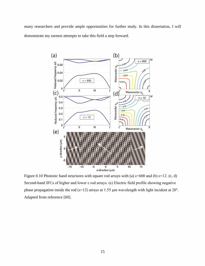
dipole resonances in cylindrical unit cells[67], [68] (Figures 1.11(a,b)), generating electric and
magnetic hot-spots between resonator dimers (Figures 1.11(f,g)), achieving super-directive
antennae radiation[69], active tuning of resonant modes[70] (Figures 1.11(c-e)), demonstration
of magnetic mirror with zero reflection phase[71], demonstration of achromatic lensing[72] and
many more. These interesting properties of dielectric metamaterials have drawn the attention of
15
many researchers and provide ample opportunities for further study. In this dissertation, I will
demonstrate my earnest attempts to take this field a step forward.
Figure 0.10 Photonic band structures with square rod arrays with (a) ε=600 and (b) ε=12. (c, d)
Second-band IFCs of higher and lower ε rod arrays. (e) Electric field profile showing negative
phase propagation inside the rod (ε=12) arrays at 1.55 μm wavelength with light incident at 20°.
Adapted from reference [60].
16
Figure 0.11 (a) Diagram illustrating an infinite array of nanodisks resonators where individual
resonators are represented as electric and magnetic dipoles for x-polarized incident light
describing a Huygens’ metasurface. b) Electric and magnetic field profiles of the magnetic (top)
and electric (bottom) mode of a silicon-nanodisk resonator. (c) Schematic of the silicon nanodisk
metasurface integrated into an LC cell. (d) SEM image of Si nanodisks arrays (top). Sketch of
the (idealized) arrangement of the LC molecules in the nematic and the isotropic phase,
respectively (bottom). (f) Comparison between metal and dielectric dimers. (g) Schematic (left)
and experimental near field measurement of electromagnetic field enhancement in the gap
between Si nano dimers (right top). SEM of nano dimer (right bottom). Adapted from references
[68] (a,b); [70] (c,d,e); [73] (f,g).
17
1.4 Organization of the Document
Chapter 2 will describe the realization of an all-dielectric zero index metamaterial (ZIM) at
optical frequencies. The design methodology will be discussed in detail, followed by discussion
on the bulk fabrication methodology. Finally realization of the ZIM will be demonstrated by
optical experiments.
In Chapter 3, I will discuss the realization of near perfect broadband reflectance from a
single layer sub-wavelength-thick all-dielectric metamaterial. The role of the fundamental modes
of the single resonator will be discussed in achieving a broad near perfect reflectance band. We
will also explore the effect of disorder on the strength of reflectance by randomizing the unit
cells in the metamaterial. Finally, we will propose a mechanism to engineer the unit cell to
broaden the high reflectance bandwidth.
Chapter 4 will be devoted to demonstration of scalability of dielectric metamaterials to
large areas (centimeter sized) using nanosphere lithography, a low cost and high throughput
patterning technique. Large scale perfect reflection will be demonstrated over large areas using a
single layer of silicon resonators. The effect of disorder on the magnetic and electric dipole
resonances will be studied and mechanisms will proposed for overcoming the influence of
disorder on reflectance. The possibility of achieving a magnetic mirror at optical frequencies will
also be explored.
In Chapter 5, I will discuss the advancement of nanosphere lithography technique to
fabricate asymmetric resonators. Here, we propose an advanced large area and high throughput
lithography technique which can control the size and orientation of asymmetric patterns spatially.
This advanced gradient lithography technique will pave the way towards simple, expedited, and
high throughput large scale fabrication of gradient metasurfaces.

18
In Chapter 6, I will summarize the accomplished work and give a perspective of future
work on dielectric metamaterials.
19
Chapter 2
Impedance-Matched All-Dielectric Optical Zero Index Metamaterial
2.1 Introduction
Epsilon near zero (ENZ) and zero index metamaterials (ZIMs) are a special class of
metamaterials which exist at the origin of the parameter space (Figure 1.2, Chapter 1). A simple
way to realize an ENZ using a metal is to operate at the plasma frequency (pω ). From the Drude-
Lorentz model (Eq. 1.4, Chapter 1), the permittivity of a metal at its plasma frequency is zero.
Control over realizing ENZ at different frequencies can be achieved by stacking thin layers[74]
or by a composite of complementary split ring resonators (SRRs) in host media[6]. Another
alternative way to design an ENZ is by utilizing the dispersive properties of metallic waveguides
which is operating near cut-off frequency of dominant waveguide mode[75]. The permittivity of
the transverse mode of a rectangular metallic waveguide can be given by,
2 2 2 2
0/ / (4 )effε ε n c f w , where, w is the width of waveguide, n is the refractive index, c is the
speed of light and f is the operating frequency. Hence, the effective permittivity is zero at the
waveguide cut-off frequency ( / 2f c wn ).
ENZs have been experimentally demonstrated in the microwave[6], [76], mid-IR[77],
and visible regimes[75]. ENZ metamaterials have a permittivity ( ) near-zero while the
permeability ( ) remains unity, resulting in a near-zero refractive index ( √ . However,
since the permeability remains finite, the relative optical impedance, ( √ is grossly
mismatched from free-space, which results in large reflections from the ENZ-air interface and
limits the functionality of ENZs.
20
Figure 0.12 (a) and (b) Dirac cone like dispersion in 2D square lattice of circular rods. (c)
Retrieved effective parameters showing cross-over at zero at Dirac point demonstrating zero
index of refraction. (d) Simulated field profile to demonstrate wave can turn through waveguide
bends with a channel composed of ZIM and any obstacle cannot be recognized because the
wavelength is infinitely long inside a ZIM. Adapted from reference [78].
The solution to overcome the issue of high reflectance is to design a zero index
metamaterial which is impedance matched to air, i.e. both permittivity and permeability are equal
to zero. Impedance matched zero refractive index has been demonstrated at optical frequencies
with a fishnet geometry[79], however, the metamaterial only functions with normal incidence of
light. A more elegant design for an impedance matched ZIM was proposed by Huang et al[78].
In their design the realization of zero refractive index is dictated by designing a periodic
structure of infinite rods which forms a Dirac cone like dispersion at the Г point in the band
diagram (Figure 2.1). Prior to this study, Wang et al [80] proposed that a Dirac cone like
dispersion can be achieved at the Г point from a hypothetical homogeneous medium with linear
dispersion varying from negative-to-zero-to-positive from lower to higher frequencies. From
21
these studies the correlation between Dirac cone like dispersion and zero index of refraction is
substantiated.
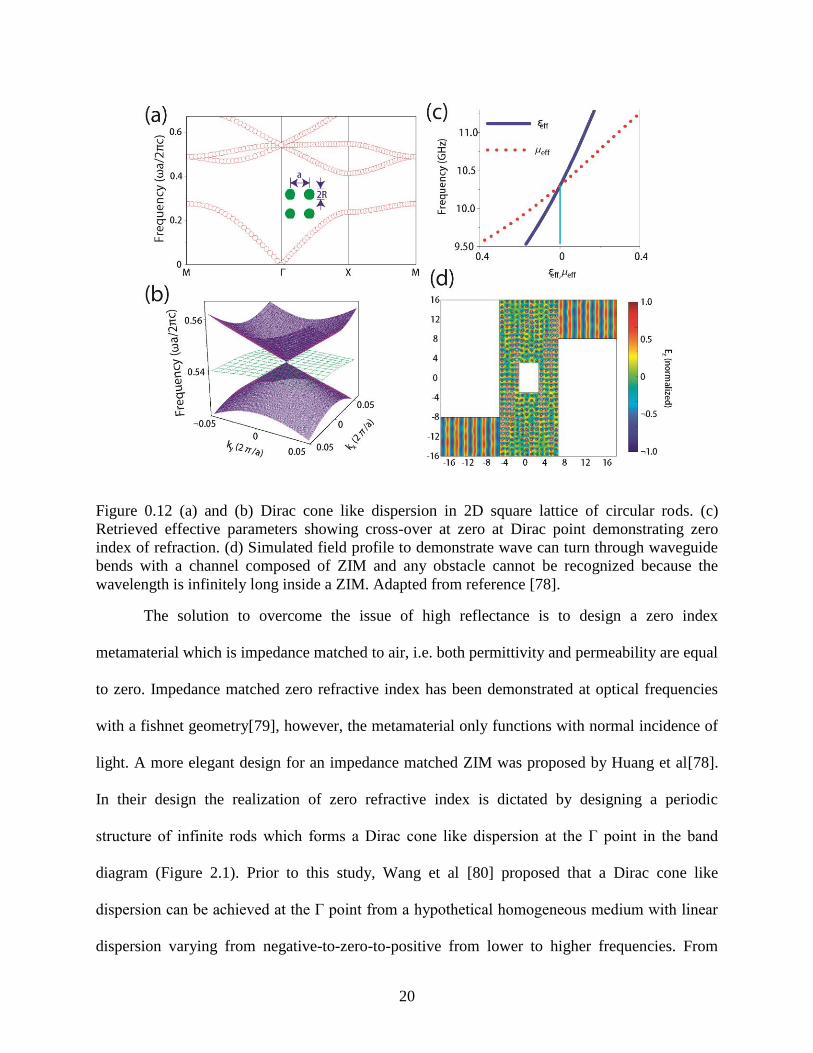
The most interesting feature of a ZIM is that the wave-vector inside such a material is
zero ( 0k ), which leads to many other interesting properties. The phase velocity, defined as
/ω k , is infinite and the effective wavelength ( /nλ λ n ) inside a ZIM is infinite as well. Hence
any object inside a ZIM will practically be cloaked because an object will not scatter light if its
size is infinitely smaller than the wavelength of light illuminating it. Another interesting feature
is that a ZIM only transmits light normal to the interface. This follows directly from Snell’s law,
1 1 2 2sin sinn θ n θ
where, n1 and n2 are the refractive indices of two different media (medium 1 and 2) and light is
incident from medium 1 to medium 2 at an angle θ1 and refracts in medium 2 with an angle of θ2.
Now, let us consider n2=0. To satisfy Snell’s law, θ1 has to be 90°. This can also be explained by
comparing the isofrequency contours (IFCs) of a ZIM and air at the interface. In Figure 2.2, the
small circle (red), corresponding to an IFC of the ZIM, has a radius 0ZIM ZIMk k n which is
proportional to the effective index of the metamaterial and the larger circle (black) has a radius
proportional to the index of air ( 1Airn ). In order to conserve angular momentum at the ZIM-air
interface light can only leave ZIM surface at an angle ( maxθ ) very close to normal to the interface.
This also explains the directional emission behavior of emitters embedded inside a ZIM[76].
2.1
22
Figure 0.13 Schematic illustrating directional emission from emitters from inside a ZIM.
This chapter illustrates the first experimental realization of zero index metamaterials
(ZIM) at optical frequencies with all dielectric constituents[81]. Although, impedance matched
zero refractive index has been demonstrated at optical frequencies with a fishnet geometry[79],
the metamaterial was restricted only to normal incidence of light. These issues have been
overcome by utilizing resonant all-dielectric metamaterial with high refractive index. Here, we
designed the ZIM at optical frequencies with periodic Si rod unit cells under TM polarization of
light. The simple geometry of the dielectric resonators along with advancements in the top-down
nano-fabrication technologies provided the possibilities of fabrication of 3D ZIMs.
23
2.2 Design Methodology
The ZIM design started with calculating the band structure of an infinitely periodic
square lattice of Si rods. When properly designed, this structure can exhibit a Dirac cone at the Γ
point in the band structure[78], a feature that is similar to the electronic band structure in
graphene[82]. At the Dirac point, the metamaterial exhibits zero effective permittivity and
permeability, resulting in an impedance matched ZIM[78]. From fabrication stand point, we
designed the metamaterial with stack of square cross-section Si rods embedded in SiO2. The
band structure corresponding to the bulk ZIM (infinitely thick), with = = 260 nm and =
600 nm, is shown in Figure 2.3(a). The band structure is computed for TM polarization with the
electric field oriented along the rod axis and the Dirac cone like dispersion can be observed at the
center of Brillouin zone where two transverse bands with linear dispersion intersect a flat quasi-
longitudinal band, resulting in triple degeneracy. We utilized field-averaging of the Bloch
modes[83] to retrieve the metamaterial’s effective bulk optical properties (Figure 2.3(b)) and
simultaneous zero-permittivity and permeability are obtained at the triple degeneracy frequency
of 211 THz ( =1422 nm). This response is directly attributable to a linear combination of
electric monopole and magnetic dipole Mie resonances within the Si rods (inset of Figure 2.3(b)),
allowing the effective constitutive parameters to be accurately extracted using effective medium
theory[84]. This was confirmed by the excellent agreement between the extracted propagation
vector, acquired using field averaging, and the computed band structure around the triple
degeneracy point (Appendix A.2). A relatively broadband impedance matched low-index region
is present around the zero-index point and over the frequency range from 215 THz to 225 THz
there exists only one propagating band, TM4, which allows us to define an effective index of
refraction for the structure for off-normal angles of incidence. The iso-frequency contours (IFCs)
24
over this frequency range are shown in Figure 2.3(c) and it can be observed that they maintain a
nearly circular shape indicating that the material maintains a relatively isotropic low-index
response for TM-polarized light over this bandwidth. This all-angle response is critical for
preserving the unique physics associated with low- or zero-index materials such as directionally
selective transmission and emission from within the material. It should be noted that in a
perfectly homogeneous zero-index metamaterial, the flat longitudinal band is not accessible with
TM-polarized light. However, due to finite spatial dispersion, this band becomes quasi-
longitudinal in our case and is accessible at off-normal angles of incidence. As can be seen from
Figure 2.3(a), the band bends down and thus prevents single mode propagation for off-normal
incidence at frequencies at and below the Dirac point (extended states of the crystal are provided
in the Appendix A.2). In this frequency region, a refractive index cannot be assigned for off-
normal incidence and directionally selective transmission is not preserved.
Figure 0.14 (a) Band diagram of uniform bulk ZIM (infinitely thick) for TM polarization. Dirac
cone dispersion is observed at the Γ point with triple degeneracy at 211 THz. The shaded area
denotes regions outside the free-space light line. (b) Retrieved effective permittivity and
permeability of the bulk ZIM acquired using field-averaging. The inset shows the electric and
magnetic fields within a single unit cell at the zero-index frequency indicating a strong electric
monopole and magnetic dipole response. (c) IFC of the TM4 band. The contours are nearly
circular (i.e., isotropic) for a broad frequency range and increase in size away from the zero-
index frequency indicating a progressively larger refractive index.
25
One of the consequences of a low or zero-index is that light will not be guided using a
conventional slab waveguide, in other words Dirac point appears in the light cone, and thus the
metamaterial must be designed for free-space access. Hence, the simulated 2D periodic infinite
rod structure needs to be designed as a 3D structure with periodicity along y and z direction, with
orientation of the rods along x. Along z direction which is the normal direction to the plane of
substrate, keeping in mind the fabrication convenience, number of unit cells needs to be
minimum. We optimized the number of unit cells as 5 based on the convergence of the zero
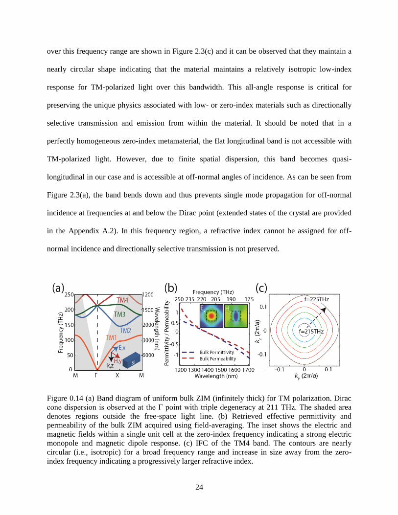
index response to the infinite periodic structure. In Fig, we show the electric and magnetic field
profiles at a frequency that is slightly above the zero-index frequency, where both the index of
refraction and magnitude of the wavevector are close to zero. This leads to negligible spatial
phase change across the length of the ZIM ( , where L is total thickness of the ZIM
structure. In the field plots (Figure 2.4), it is clear that the transmitted light leaves the ZIM / air
interface with the same phase as the incident plane wave. The unit cells also show strong electric
and magnetic resonances, which are resonating in-phase, a characteristics that can be attributed
to infinite phase velocity leading to zero phase lag between the resonators.
26
Figure 0.15 Electric and magnetic field plots demonstrating no spatial phase change of light
across the ZIM. All the Si resonators are resonating in phase because of infinite phase velocity
inside the ZIM.
2.3 Fabrication of Multilayer ZIM
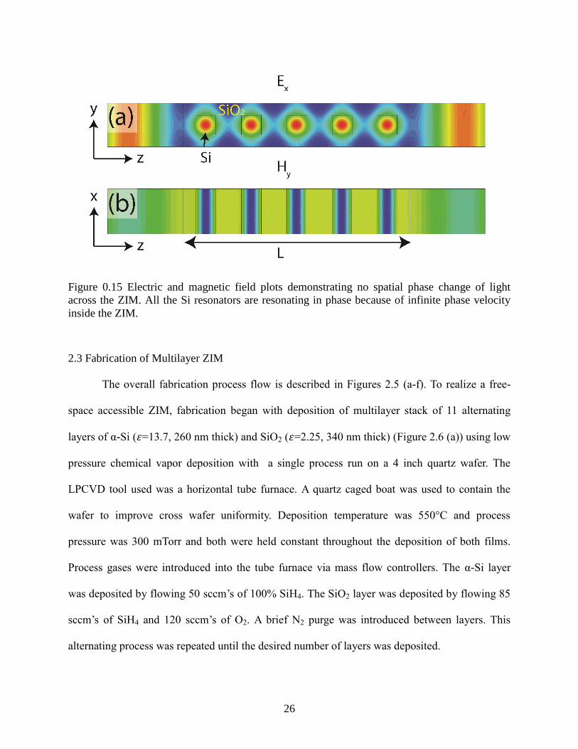
The overall fabrication process flow is described in Figures 2.5 (a-f). To realize a free-
space accessible ZIM, fabrication began with deposition of multilayer stack of 11 alternating
layers of α-Si ( =13.7, 260 nm thick) and SiO2 ( =2.25, 340 nm thick) (Figure 2.6 (a)) using low
pressure chemical vapor deposition with a single process run on a 4 inch quartz wafer. The
LPCVD tool used was a horizontal tube furnace. A quartz caged boat was used to contain the
wafer to improve cross wafer uniformity. Deposition temperature was 550°C and process
pressure was 300 mTorr and both were held constant throughout the deposition of both films.
Process gases were introduced into the tube furnace via mass flow controllers. The α-Si layer
was deposited by flowing 50 sccm’s of 100% SiH4. The SiO2 layer was deposited by flowing 85
sccm’s of SiH4 and 120 sccm’s of O2. A brief N2 purge was introduced between layers. This
alternating process was repeated until the desired number of layers was deposited.
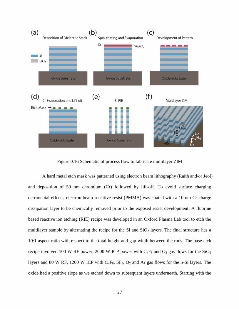
27
Figure 0.16 Schematic of process flow to fabricate multilayer ZIM
A hard metal etch mask was patterned using electron beam lithography (Raith and/or Jeol)
and deposition of 50 nm chromium (Cr) followed by lift-off. To avoid surface charging
detrimental effects, electron beam sensitive resist (PMMA) was coated with a 10 nm Cr charge
dissipation layer to be chemically removed prior to the exposed resist development. A fluorine
based reactive ion etching (RIE) recipe was developed in an Oxford Plasma Lab tool to etch the
multilayer sample by alternating the recipe for the Si and SiO2 layers. The final structure has a
10:1 aspect ratio with respect to the total height and gap width between the rods. The base etch
recipe involved 100 W RF power, 2000 W ICP power with C4F8 and O2 gas flows for the SiO2
layers and 80 W RF, 1200 W ICP with C4F8, SF6, O2 and Ar gas flows for the α-Si layers. The
oxide had a positive slope as we etched down to subsequent layers underneath. Starting with the
28
base recipe for the upper layers, the subsequent SiO2 layers were etched more aggressively with
increasing depth. This was accomplished by changing the ratio of C4F8 and O2 gas-flow which
provided less passivation to the side walls during etching. The base Si etch recipe resulted in
straight side walls until we reached the bottom most layer. The bottom most oxide and Si layers
were etched with the most aggressive recipes and the top layers were protected by additional
passivation steps. The metamaterial’s internal structure was characterized by imaging the edge
profile after milling cross-sections inside the array using focused ion beam milling (FIB). During
all imaging, a thin layer of Cr was deposited on the sample to provide a conducting surface. A
total of 5 functional layers (Si / SiO2 pairs) results in a metamaterial with a thickness of 3 μm,
about twice the free-space wavelength at the zero-index point (Figure 2.6 (b)).
We made sure that PMMA, which was spin-coated on the sample after the RIE process,
filled in the gaps completely in order to provide a background with the same permittivity as the
SiO2 spacer layers. The sample with a drop casted PMMA film was placed in an evacuated
desiccator to remove air bubbles and this process was followed by spinning and soft baking (120
degrees for 2 minutes) twice and reflowing at 300˚ C for 2 minutes to reach the desired
thickness. The final structure was cross-sectioned with FIB milling at multiple locations to
confirm the complete filling (Figure 2.6 (c)).
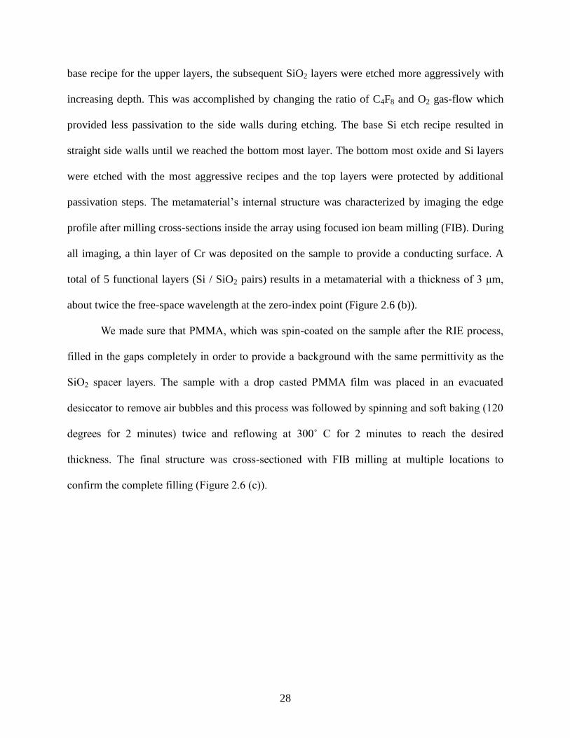
29
Figure 0.17 (a) SEM image of multilayer stack of Si and SiO2. (b) FIB image (isometric view) of
ZIM (before PMMA filling). (c) Cross-sectional FIB showing complete filling of PMMA inside
the gap regions.
2.4 Influence of Non-Uniformity
The fabricated metamaterial has both a finite thickness as well as non-uniform rod sizes
and will thus deviate somewhat from the bulk parameters. To better understand the optical
response of the fabricated metamaterial, full-wave finite-difference time-domain (FDTD)
simulations were assigned with optical properties for arbitrary angles of incidence due to
presence of the quasi-longitudinal band which is accessible at large incident angles.
In order to gauge the agreement with the simulated material properties, transmittance of
the fabricated ZIM was acquired by illuminating the sample with normal-incident white light
with the electric field oriented along the Si rod axis (Figure 2.7(c)). The simulated and measured
transmittance show good agreement in spectral shape, though the experimentally obtained curve
has a lower amplitude that is likely due to non-uniformity in rod width at the edges of the sample
as well as surface roughness. The measured spectrum shows a peak transmission of 80% at 1405
nm, the spectral position corresponding to the impedance-matched low-index point. A dip in
transmission also occurs at 1460 nm, corresponding to the metallic region of the sample.

30
Figure 0.18 (a) Effective permittivity and permeability of the fabricated ZIM obtained using S-
parameter retrieval. Regions corresponding positive index, metallic properties, and negative
index are denoted with blue, grey, and yellow shading, respectively. (b) Effective refractive
index of the fabricated structured obtained using S-parameter retrieval. (c) Experimental (red)
and theoretical transmittance (dotted blue) curves of the ZIM (200 x 200 µm2
total pattern area).
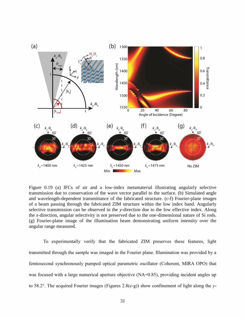
2.5 Experimental Characterization of the ZIM
One of the most fascinating properties of isotropic low-index materials is that light
incident from free-space is only transmitted over a narrow range of incidence angles. This effect
is a direct consequence of phase matching at the interface which requires that the wave vector
along the interface be conserved. As illustrated with the IFCs depicted in Figure 2.8(a), in a low-
index metamaterial, the wavevector is restricted to extremely small values causing light incident
at high angles ( 𝑦 > | 𝑍𝐼𝑀|) to be reflected while near-normal incident light is transmitted
( 𝑦 < | 𝑍𝐼𝑀|). This effect is evident when examining the simulated transmittance with regard
to wavelength and angle of incidence (Figure 2.8(b)) for the fabricated ZIM. The material
exhibits near-zero transmission at off-normal incident angle within the positive index band
centered at 1400 nm, with improving angular confinement in transmission as we approach the
zero-index point. The presence of the quasi-longitudinal band within the negative index region
( ~1475 nm) is also apparent, allowing transmission at large incident angles.
31
Figure 0.19 (a) IFCs of air and a low-index metamaterial illustrating angularly selective
transmission due to conservation of the wave vector parallel to the surface. (b) Simulated angle
and wavelength-dependent transmittance of the fabricated structure. (c-f) Fourier-plane images
of a beam passing through the fabricated ZIM structure within the low index band. Angularly
selective transmission can be observed in the y-direction due to the low effective index. Along
the x-direction, angular selectivity is not preserved due to the one-dimensional nature of Si rods.
(g) Fourier-plane image of the illumination beam demonstrating uniform intensity over the
angular range measured.
To experimentally verify that the fabricated ZIM preserves these features, light
transmitted through the sample was imaged in the Fourier plane. Illumination was provided by a
femtosecond synchronously pumped optical parametric oscillator (Coherent, MIRA OPO) that
was focused with a large numerical aperture objective (NA=0.85), providing incident angles up
to 58.2°. The acquired Fourier images (Figures 2.8(c-g)) show confinement of light along the y-
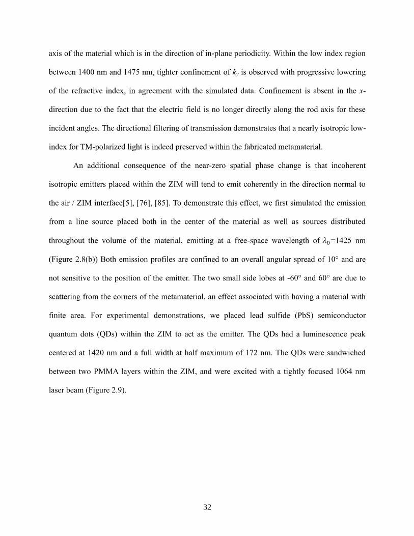
32
axis of the material which is in the direction of in-plane periodicity. Within the low index region
between 1400 nm and 1475 nm, tighter confinement of ky is observed with progressive lowering
of the refractive index, in agreement with the simulated data. Confinement is absent in the x-
direction due to the fact that the electric field is no longer directly along the rod axis for these
incident angles. The directional filtering of transmission demonstrates that a nearly isotropic low-
index for TM-polarized light is indeed preserved within the fabricated metamaterial.
An additional consequence of the near-zero spatial phase change is that incoherent
isotropic emitters placed within the ZIM will tend to emit coherently in the direction normal to
the air / ZIM interface[5], [76], [85]. To demonstrate this effect, we first simulated the emission
from a line source placed both in the center of the material as well as sources distributed
throughout the volume of the material, emitting at a free-space wavelength of =1425 nm
(Figure 2.8(b)) Both emission profiles are confined to an overall angular spread of 10° and are
not sensitive to the position of the emitter. The two small side lobes at -60° and 60° are due to
scattering from the corners of the metamaterial, an effect associated with having a material with
finite area. For experimental demonstrations, we placed lead sulfide (PbS) semiconductor
quantum dots (QDs) within the ZIM to act as the emitter. The QDs had a luminescence peak
centered at 1420 nm and a full width at half maximum of 172 nm. The QDs were sandwiched
between two PMMA layers within the ZIM, and were excited with a tightly focused 1064 nm
laser beam (Figure 2.9).

33
Figure 0.20 QD Emission Spectrum. Photoluminescence (PL) spectrum of PbS quantum dots
(Evident Technology) used in the main text. The emission peak appears at 1425 nm, with a full-
width at half-maximum of 172 nm. The blue-, gray- and yellow-shaded region corresponds to
positive index, metallic properties, and negative index as acquired from S-parameter retrieval.
The dip of measured luminescence spectrum at around 1380 nm is due to the water absorption
line.
The Fourier-plane images (Figures 2.10(c-f)) from both an unstructured PMMA/QD film
and QDs placed within the metamaterial show good angular confinement in the y-direction and
an over two-fold increase in intensity emitted normal to the interface from the ZIM compared to
the unstructured case. The increase in emission normal to the interface is a result of the uniform
phase distribution within the ZIM, leading to constructive interference from emitters throughout
the material[75], further supporting the realization of a near-zero refractive index. The
constructive interference of multiple emitters is in competition with the reduced optical density
of states associated with the low-index response. For instance, if the number of emitters is
reduced to one, the emitted power in air will be greater than the ZIM in all directions. However,
as expected for constructive interference within the material, the far-field intensity of waves
34
propagating normal to the interface is proportional to the number of emitters squared. We also
note that although the luminescence peak of the QDs matches the low-index band of fabricated
ZIM structure quite closely, parts of the emission fall beyond the low-index band, resulting in
slightly lower angular confinement compared with the transmission data.
Figure 0.21 (a) Schematic of laser-pumped QD emission from within the ZIM structure. (b)
Calculated emission profile for a line source placed in the center of the material (centered) and
the average profile from line sources placed throughout the material (averaged). (c) 2D Fourier-
plane images of quantum dot emission on the substrate, intensity is scaled by two times. (d) A
cross-section of the emission taken at kx = 0. (e) 2D Fourier-plane images of QD emission within
the ZIM, respectively, showing enhanced rate and directivity of spontaneous emission. (f) A
cross-section of the emission taken at kx = 0.
35
2.6 Conclusion
Here we developed a mechanism to experimentally realize an impedance matched and
lossless isotropic zero index metamaterial, consisting of all dielectric rod unit cells, at optical
frequencies for a particular polarization (TM) of light. We exploited the electric and magnetic
Mie resonances in single dielectric resonator and designed the ZIM with periodic square lattice
of collection of such resonators, exhibiting simultaneous zero effective permittivity and
permeability. The experimental demonstration of angular selectivity of transmission and
spontaneous emission illustrates the practical realization of isotropic ZIM for TM polarized light.
The realization of impedance matched ZIMs at optical frequencies opens new avenues towards
the development of angularly selective optical filters, directional light sources, and large area
single mode photonic devices. The advent of all-dielectric optical metamaterials provides a new
route to developing novel optical metamaterials with both low absorption loss and isotropic
optical properties. Proper understanding of controlling electric and magnetic Mie resonances
opens the door to other applications such as perfect reflection using single layer all-dielectric
metamaterial structures, which we will explore in the next chapter.
36
Chapter 3
Mie Resonance Based All-Dielectric Metamaterial Perfect Reflectors
3.1 Introduction
In this chapter, we exploit the electric and magnetic Mie dipole resonances of silicon (Si)
cylinder resonators to design a single negative metamaterial with polarization independent near-
perfect broadband reflection within the telecommunication band. The study is also extended to
disordered metamaterials which demonstrates that near-unity reflection can be preserved by
avoiding interactions between resonators. We also explore the opportunities for broadening the
reflectance bandwidth by utilizing higher order resonances along with the fundamental
resonances. This has been achieved by manipulating the resonances with more complex
resonator design.
Perfect dielectric reflectors are important photonic elements due to their ability to handle
high power irradiation. Although gold (Au) and silver (Ag) mirrors exhibit high reflection
(~98 %) in the telecommunication band, they are not suitable for high-power applications due to
their absorption (~2 %). In place of metallic mirrors, distributed Bragg reflectors (DBRs), made
of alternating dielectric layers, are typically used for achieving near-perfect reflection. The
primary disadvantage of Bragg reflectors is that the deposition of multiple dielectric materials is
a lengthy process which adds to the cost of the product. Realization of perfect reflection from a
single-layer disorder metamaterial offers advantages in terms of possibilities of simple, high-
throughput, and low-cost fabrication, and in turn opens the door to future paint-like coatings of
metamaterials for even larger-area implementation.
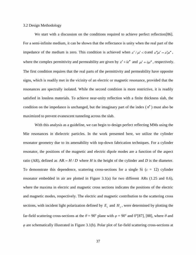
37
3.2 Design Methodology
We start with a discussion on the conditions required to achieve perfect reflection[86].
For a semi-infinite medium, it can be shown that the reflectance is unity when the real part of the
impedance of the medium is zero. This condition is achieved when / 0 and ,
where the complex permittivity and permeability are given by i and i , respectively.
The first condition requires that the real parts of the permittivity and permeability have opposite
signs, which is readily met in the vicinity of an electric or magnetic resonance, provided that the
resonances are spectrally isolated. While the second condition is more restrictive, it is readily
satisfied in lossless materials. To achieve near-unity reflection with a finite thickness slab, the
condition on the impedance is unchanged, but the imaginary part of the index ( n ) must also be
maximized to prevent evanescent tunneling across the slab.
With this analysis as a guideline, we can begin to design perfect reflecting MMs using the
Mie resonances in dielectric particles. In the work presented here, we utilize the cylinder
resonator geometry due to its amenability with top-down fabrication techniques. For a cylinder
resonator, the positions of the magnetic and electric dipole modes are a function of the aspect
ratio (AR), defined as AR /H D where H is the height of the cylinder and D is the diameter.
To demonstrate this dependence, scattering cross-sections for a single Si (ε = 12) cylinder
resonator embedded in air are plotted in Figure 3.1(a) for two different ARs (1.25 and 0.6),
where the maxima in electric and magnetic cross sections indicates the positions of the electric
and magnetic modes, respectively. The electric and magnetic contribution to the scattering cross
sections, with incident light polarization defined by xE and yH , were determined by plotting the
far-field scattering cross-sections at the θ = 90° plane with φ = 90° and 0°[87], [88], where θ and
φ are schematically illustrated in Figure 3.1(b). Polar plot of far-field scattering cross-sections at
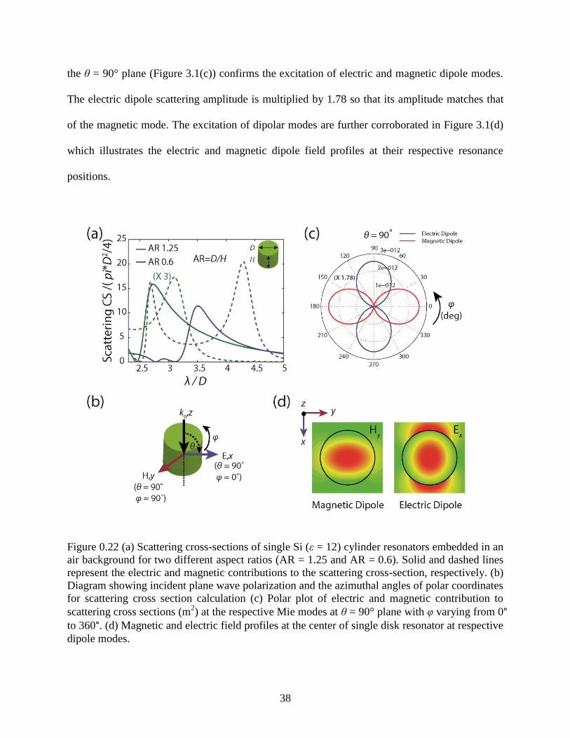
38
the θ = 90° plane (Figure 3.1(c)) confirms the excitation of electric and magnetic dipole modes.
The electric dipole scattering amplitude is multiplied by 1.78 so that its amplitude matches that
of the magnetic mode. The excitation of dipolar modes are further corroborated in Figure 3.1(d)
which illustrates the electric and magnetic dipole field profiles at their respective resonance
positions.
Figure 0.22 (a) Scattering cross-sections of single Si (ε = 12) cylinder resonators embedded in an
air background for two different aspect ratios (AR = 1.25 and AR = 0.6). Solid and dashed lines
represent the electric and magnetic contributions to the scattering cross-section, respectively. (b)
Diagram showing incident plane wave polarization and the azimuthal angles of polar coordinates
for scattering cross section calculation (c) Polar plot of electric and magnetic contribution to
scattering cross sections (m2) at the respective Mie modes at θ = 90° plane with φ varying from 0°
to 360°. (d) Magnetic and electric field profiles at the center of single disk resonator at respective
dipole modes.
39
To illustrate the spectral separation of electric and magnetic modes across a larger
domain, the corresponding mode positions are plotted against the AR in Figure 3.2(a). At low
ARs we find that the electric mode is the first resonance and increasing the AR results in a mode
crossing. Further increasing the AR results in spectral separation of the modes with the largest
spacing occurring at an AR ~ 1.0. After this point, increasing the AR results in slight reduction
of the spectral separation and eventual saturation in the spacing of the modes. To better
understand the collective response of a metamaterial formed from these resonators, the
reflectance of an array of resonators is shown in Figure 3.2(b). As expected, the reflectance
bandwidth is maximized at ARs corresponding to the largest separation between the modes.
Furthermore, as the AR is reduced, complete modal overlap occurs, leading to a wavelength at
which the resonator is impedance matched to air and a narrow transmission window appears.
This effect has previously been studied for cylinder resonators as one way to achieve complete
suppression of backscattering[67].
At AR ~1.0, there is also a slight dip in the middle of the reflectance band. This dip can
be understood by the fact that this region is far from either resonance and thus and are
small, reducing the magnitude of n and thus reducing the strength of the reflectance. Large
ARs also result in weakening of the electric and magnetic dipole resonances and a subsequent
reduction in the bandwidth of the response. In the design of broadband reflectors, caution must
therefore be taken to ensure that spectral separation between the modes and weakening of the
resonances does not adversely affect the average reflection across the band.
40
Figure 0.23 (a) Spectral positions of the electric and magnetic dipole Mie resonances as a
function of the AR. The solid lines are fitted to the points as a guide for the eye. (b) Simulated
reflectance plots for periodic Si cylinder metamaterials, illustrating reflectance as a function of
cylinder AR.
With these studies as a guideline, we have chosen a Si cylinder resonator-based
metamaterial with H = 500 nm, D = 400 nm (AR = 1.25), and a periodicity of 660 nm for
experimental studies. This particular AR and cylinder geometry was chosen as it preserves a
broad reflection band while the band’s position remains within the measurable range of our
microscopy setup. It should also be noted that in experimental studies, H was constrained by the
wafers used to realize the metamaterials, as outlined below. To better understand the
metamaterial’s response, full-wave simulations were performed using the Floquet mode solver
using the commercial finite-element code HFSS (Ansys). S-parameter retrieval[89]–[91] was
used to extract the effective optical properties. These simulations were performed for Si
resonators, in air, with a permittivity equal to that of our experimental samples which was
measured with spectroscopic ellipsometry. As illustrated in Figures 3.2(a,b), the metamaterial is
single negative with 0 and 0 between 1315 nm and 1500 nm. This leads to an extreme
impedance mismatch with 0z across this bandwidth, as shown in Figure 3.2(c). Within this
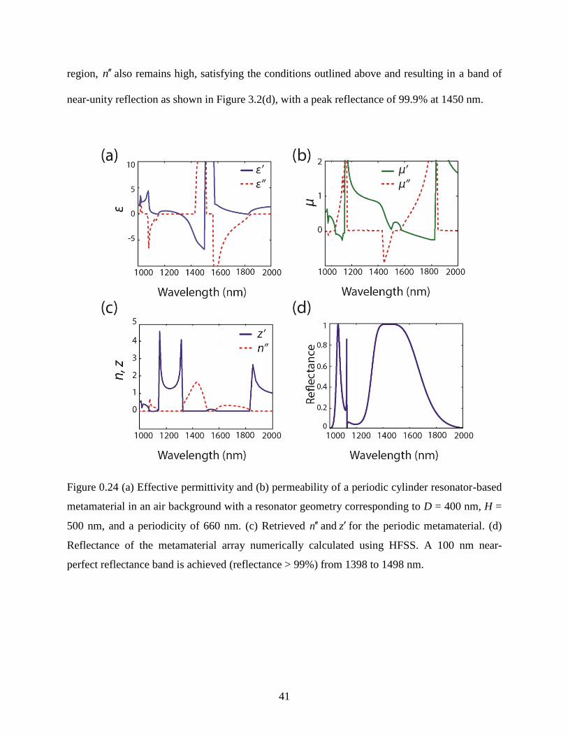
41
region, n also remains high, satisfying the conditions outlined above and resulting in a band of
near-unity reflection as shown in Figure 3.2(d), with a peak reflectance of 99.9% at 1450 nm.
Figure 0.24 (a) Effective permittivity and (b) permeability of a periodic cylinder resonator-based
metamaterial in an air background with a resonator geometry corresponding to D = 400 nm, H =
500 nm, and a periodicity of 660 nm. (c) Retrieved n and z for the periodic metamaterial. (d)
Reflectance of the metamaterial array numerically calculated using HFSS. A 100 nm near-
perfect reflectance band is achieved (reflectance > 99%) from 1398 to 1498 nm.
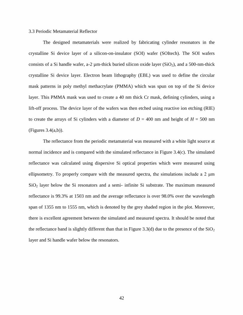
42
3.3 Periodic Metamaterial Reflector
The designed metamaterials were realized by fabricating cylinder resonators in the
crystalline Si device layer of a silicon-on-insulator (SOI) wafer (SOItech). The SOI wafers
consists of a Si handle wafer, a-2 µm-thick buried silicon oxide layer (SiO2), and a 500-nm-thick
crystalline Si device layer. Electron beam lithography (EBL) was used to define the circular
mask patterns in poly methyl methacrylate (PMMA) which was spun on top of the Si device
layer. This PMMA mask was used to create a 40 nm thick Cr mask, defining cylinders, using a
lift-off process. The device layer of the wafers was then etched using reactive ion etching (RIE)
to create the arrays of Si cylinders with a diameter of D = 400 nm and height of H = 500 nm
(Figures 3.4(a,b)).
The reflectance from the periodic metamaterial was measured with a white light source at
normal incidence and is compared with the simulated reflectance in Figure 3.4(c). The simulated
reflectance was calculated using dispersive Si optical properties which were measured using
ellipsometry. To properly compare with the measured spectra, the simulations include a 2 μm
SiO2 layer below the Si resonators and a semi- infinite Si substrate. The maximum measured
reflectance is 99.3% at 1503 nm and the average reflectance is over 98.0% over the wavelength
span of 1355 nm to 1555 nm, which is denoted by the grey shaded region in the plot. Moreover,
there is excellent agreement between the simulated and measured spectra. It should be noted that
the reflectance band is slightly different than that in Figure 3.3(d) due to the presence of the SiO2
layer and Si handle wafer below the resonators.
43
Figure 0.25 (a) Top and (b) isometric SEM images of periodic Si cylinder-based metamaterials.
The scale bars in the images are equal to 1 µm. (c) Comparison between the numerically
calculated and measured reflectance spectra of the metamaterials. The average reflectance
between 1355 nm and 1555 nm (grey shaded region) is over 98.0%.
3.4 Disordered Metamaterial Reflector
One of the benefits of using metamaterials over photonic band gap materials is that their
response should, ideally, not be a strong function of the periodicity. This is because the
resonance is isolated to the unit cell, and the absence of coupling between unit cells ensures that
resonance is not spectrally shifted upon distortion of the lattice. To investigate the effect of
periodicity on the perfect reflectors, we have explored the reflectance from disordered
arrangements of the cylinders in the metamaterials. The metamaterials were designed with
periodic 2 by 2 and 3 by 3 resonator supercells and the position of each resonator within the
44
supercell was randomized by offsetting them from their perfectly periodic x and y positions. The
perfectly periodic positions for each sample are based on a resonator spacing of 660 nm, the
same spacing that is used for the metamaterials presented in Figure 3.4. The disorder was
quantified by computing the standard deviation in the distances between the four nearest
neighbors to each resonator in the supercell and then normalizing this by the periodicity of the
perfectly ordered array.
Metamaterials with 5 different levels of disorder, equal to 6%, 9%, 15%, 15% and 17%
were modeled and experimentally measured for both Ex and Ey polarizations at normal incidence
(Figures 3.5(a-e)). Figures 3.5(a-d) correspond to 2 by 2 resonator supercells and Figure 3.5(e)
corresponds to a 3 by 3 resonator supercell configuration. Each metamaterial configuration is
illustrated by SEM images of the fabricated structure in the inset of the figure. The reflectance
from the disordered structures agree well with the simulated curves for both polarizations and
exhibit a reflection band that is ~180 nm wide. The maximum reflectance value within the band
decreases as the percentage disorder increases, with a maximum reflectance of 98.3%, 96.8%,
91.9%, 92.0% and 86.8% for Ex polarized incidence and 97.1%, 95.8%, 93.1%, 91.0% and 79.9%
for Ey polarized incidence.
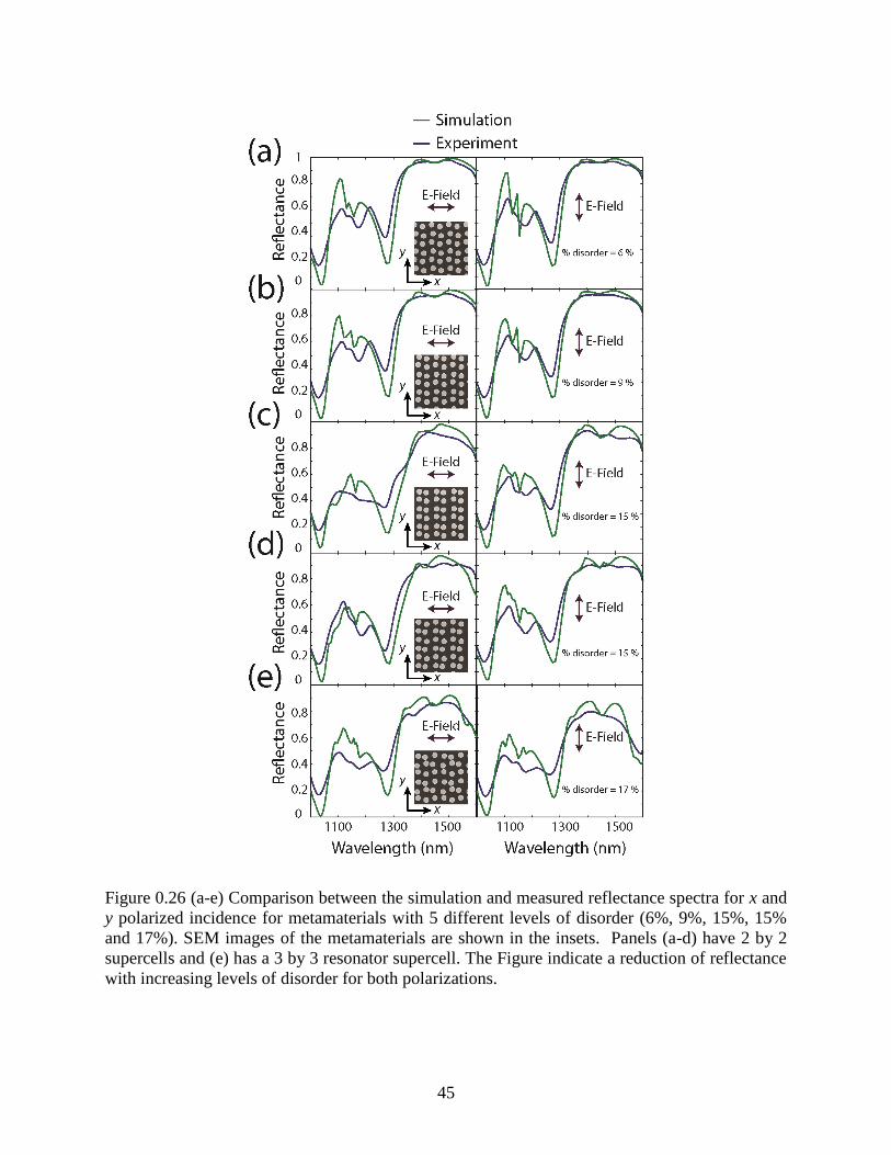
45
Figure 0.26 (a-e) Comparison between the simulation and measured reflectance spectra for x and
y polarized incidence for metamaterials with 5 different levels of disorder (6%, 9%, 15%, 15%
and 17%). SEM images of the metamaterials are shown in the insets. Panels (a-d) have 2 by 2
supercells and (e) has a 3 by 3 resonator supercell. The Figure indicate a reduction of reflectance
with increasing levels of disorder for both polarizations.

46
The correlation between the strength of disorder and the reduction in reflectance is
attributed to spatial variations in the coupling between resonators. For large disorders, cylinders
within the supercell have different separations and thus different coupling strengths. Spatial
variations in the coupling strengths cause the resonances to shift, leading to spatial variations in ε
and µ within the supercell. This is illustrated by the far-field scattering cross-sections of a
cylinder dimer, plotted as a function of separation, in Figure 3.6(a). It can be observed that
narrowing of the gap between the particles leads to blue-shifting of the magnetic dipole
resonance, causing it to converge with the electric dipole resonance. Moreover, because the
supercell periodicity for the disordered structure is comparable to the wavelength of light within
the reflection band, the spatial variations in ε and µ within the supercell lead to the diffraction of
light into higher order reflection and transmission modes. This is illustrated in Figure 3.6(b)
where we plot the calculated total and 0th
order (specular) reflection and transmission of the
disordered metamaterial corresponding to Figure 3.5(e). It can be observed that while the total
reflection remains high, the specular reflection is reduced due to loss to higher order modes.
This issue is not present in the lightly disordered metamaterials in Figures 3.5(a,b) as their
spacing remains large enough to prevent significant coupling between the resonators. So, while
near-perfect reflection from single layer is not limited to periodic structures, the resonators must
be prevented from coming in close proximity to one another. It should be noted that this level of
control is potentially achievable when utilizing nanosphere lithography by managing the
electrostatic repulsion between the dielectric spheres used for masking[92].
One way to reduce the transmission to higher order modes is to utilize a low index
substrate. For instance, we found that some of the 0th
order reflectance can be recovered by
replacing the SiO2 / Si substrate with porous Si with an index of 1.1, which supports fewer
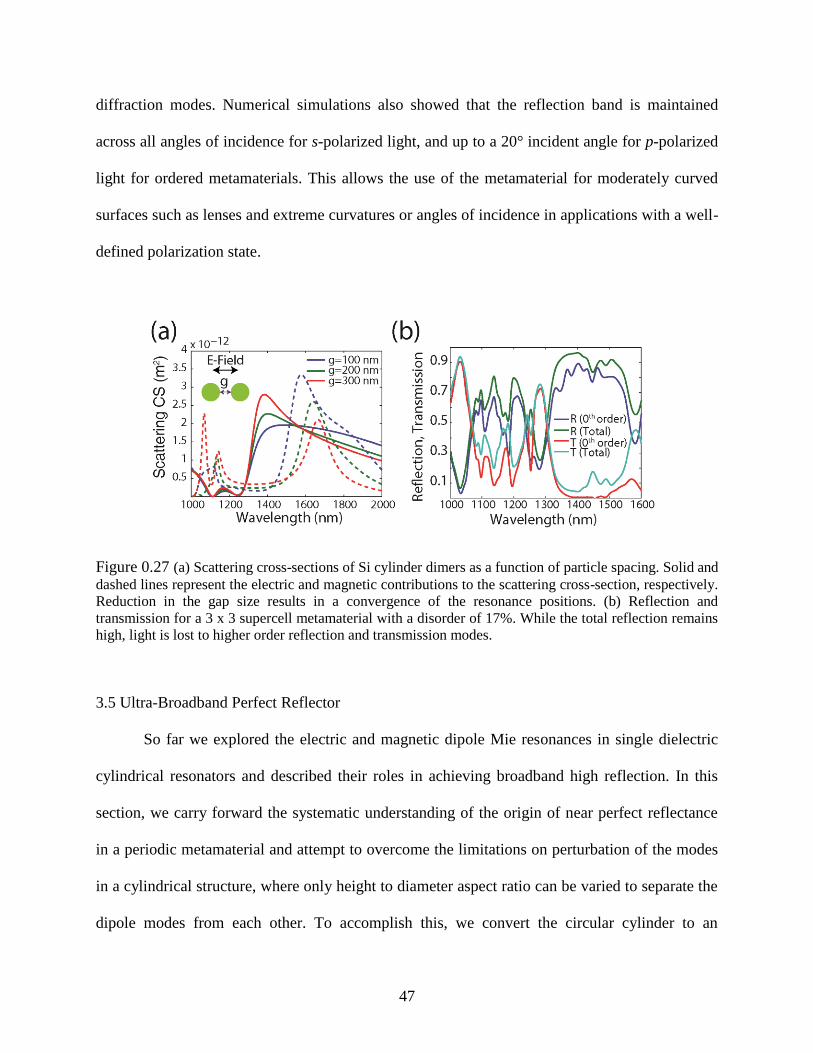
47
diffraction modes. Numerical simulations also showed that the reflection band is maintained
across all angles of incidence for s-polarized light, and up to a 20° incident angle for p-polarized
light for ordered metamaterials. This allows the use of the metamaterial for moderately curved
surfaces such as lenses and extreme curvatures or angles of incidence in applications with a well-
defined polarization state.
Figure 0.27 (a) Scattering cross-sections of Si cylinder dimers as a function of particle spacing. Solid and
dashed lines represent the electric and magnetic contributions to the scattering cross-section, respectively.
Reduction in the gap size results in a convergence of the resonance positions. (b) Reflection and
transmission for a 3 x 3 supercell metamaterial with a disorder of 17%. While the total reflection remains
high, light is lost to higher order reflection and transmission modes.
3.5 Ultra-Broadband Perfect Reflector
So far we explored the electric and magnetic dipole Mie resonances in single dielectric
cylindrical resonators and described their roles in achieving broadband high reflection. In this
section, we carry forward the systematic understanding of the origin of near perfect reflectance
in a periodic metamaterial and attempt to overcome the limitations on perturbation of the modes
in a cylindrical structure, where only height to diameter aspect ratio can be varied to separate the
dipole modes from each other. To accomplish this, we convert the circular cylinder to an
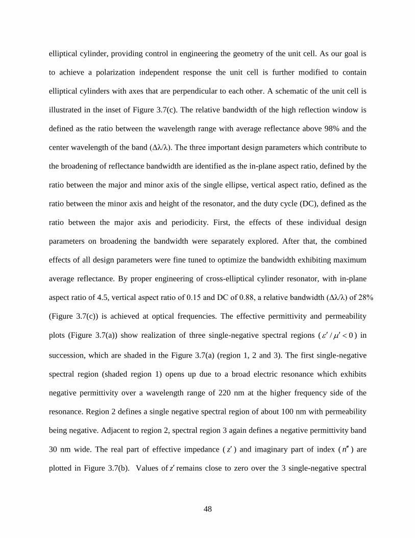
48
elliptical cylinder, providing control in engineering the geometry of the unit cell. As our goal is
to achieve a polarization independent response the unit cell is further modified to contain
elliptical cylinders with axes that are perpendicular to each other. A schematic of the unit cell is
illustrated in the inset of Figure 3.7(c). The relative bandwidth of the high reflection window is
defined as the ratio between the wavelength range with average reflectance above 98% and the
center wavelength of the band (Δλ/λ). The three important design parameters which contribute to
the broadening of reflectance bandwidth are identified as the in-plane aspect ratio, defined by the
ratio between the major and minor axis of the single ellipse, vertical aspect ratio, defined as the
ratio between the minor axis and height of the resonator, and the duty cycle (DC), defined as the
ratio between the major axis and periodicity. First, the effects of these individual design
parameters on broadening the bandwidth were separately explored. After that, the combined
effects of all design parameters were fine tuned to optimize the bandwidth exhibiting maximum
average reflectance. By proper engineering of cross-elliptical cylinder resonator, with in-plane
aspect ratio of 4.5, vertical aspect ratio of 0.15 and DC of 0.88, a relative bandwidth (Δλ/λ) of 28%
(Figure 3.7(c)) is achieved at optical frequencies. The effective permittivity and permeability
plots (Figure 3.7(a)) show realization of three single-negative spectral regions ( / 0 ) in
succession, which are shaded in the Figure 3.7(a) (region 1, 2 and 3). The first single-negative
spectral region (shaded region 1) opens up due to a broad electric resonance which exhibits
negative permittivity over a wavelength range of 220 nm at the higher frequency side of the
resonance. Region 2 defines a single negative spectral region of about 100 nm with permeability
being negative. Adjacent to region 2, spectral region 3 again defines a negative permittivity band
30 nm wide. The real part of effective impedance ( z ) and imaginary part of index ( n ) are
plotted in Figure 3.7(b). Values of z remains close to zero over the 3 single-negative spectral
49
regions and n shows 4 consecutive peaks within these regions confirming realization of perfect
reflection at the respective peak positions based on the analysis in section 3.2.1. The spectral
positions corresponding to perfect reflection are marked with dashed lines in Figures 3.7(a,b) and
with arrows in Figure 3.7(c).
Figure 0.28 (a) Real parts of effective permittivity and permeability of metamaterial formed from
cross-elliptical cylinder unit cell arranged in 2D square lattice. The shaded spectral regions (1, 2
and 3) demonstrate the region with single negative metamaterial response. (b) Real part of
effective impedance (z’) and imaginary part of effective index (n”). In Figs (a,b) the condition
for achieving unity reflection is demonstrated with dashed lines. (c) Broadband near perfect
reflectance from the metamaterial structure. Schematic of the unit cell geometry is illustrated in
the inset. A broad bandwidth (Δλ/λ=28%) with average reflectance of 98% is achieved in the
optical frequencies.
We recognize that broadband high reflectance can be achieved with Bragg reflectors.
However, the fabrication of a Bragg reflector requires deposition of multiple layers of alternating
(high and low permittivity) dielectric materials, which makes the fabrication expensive and
complicated. An alternate route to achieve broadband high reflectance at optical frequencies with
a single layer of patterned structures has been proposed in terms of high contrast gratings (HCG)
[93], [94]. In spite of matching bandwidth and reflectance strength with a Bragg reflector, HCGs
suffers from a polarization dependent response. Metamaterials composed of periodic arrays
50
single layer of cross-elliptical cylinders, on the other hand, have a polarization independent
response with a bandwidth and reflectance comparable to HCGs. Dielectric unit cells in the form
of cross-elliptical cylinders could also be used to explore other novel properties such as a
negative index.
3.6 Conclusion
In conclusion, the electric and magnetic dipole modes of single Si cylindrical resonators
have been manipulated by changing the cylinder height to diameter aspect ratio. Separating the
dipole modes leads to the formation of a single negative metamaterial with an extreme
impedance mismatch, which, along with satisfying the condition of large imaginary effective
index, results in broadband near perfect reflectance. Furthermore, since the metamaterial
response is dominated by the Mie resonances in the individual resonators, it is tolerant to
disorder in the lattice, so long as significant coupling between resonators is avoided. The
potential to achieve near-perfect reflection with a compact disordered MMs opens the door to
large-area fabrication using low-cost and high-throughput patterning techniques such as
nanosphere lithography, which we will discuss in the next chapter. Furthermore, a general
mechanism to broaden the high reflectance bandwidth is provided by manipulating the
fundamental as well as higher order resonances by controlling the dielectric resonator shape.
51
Chapter 4
Large-Scale Metamaterial Perfect Reflectors
4.1 Introduction
In Chapter 3, electron beam lithography was used for a proof-of-concept demonstration
of a dielectric metamaterial reflector with a sample size of 100 m x 100 m. However, for
large-area applications, electron beam lithography is impractical. Here, we describe the design
and fabrication of large-scale (centimeter-sized) MM perfect reflectors based on silicon (Si)
cylinder resonators. Cylindrical resonators are a particularly interesting unit cell design because
they allow spectral separation of the electric and magnetic Mie resonances by changing the
aspect ratio, and can be patterned by self-assembly based nanosphere lithography, a low-cost and
high-throughput fabrication technique. Using this platform, we demonstrate near-perfect
reflection over large centimeter-sized areas with around half a billion resonators comprising the
metamaterial. In addition, by studying the effect of lattice disorder originating from the self-
assembly patterning process, it was found that the reflectance due to the magnetic resonance is
more tolerant to disorder than the electric resonance due to better confinement of the optical
mode. This research could lead to the use of large-scale perfect reflectors within the
telecommunication band for large-area applications.
Additionally, the metamaterial approach provides the freedom to manipulate both the
magnetic and electric response of the reflector. Conventional mirrors made from metal and
Bragg reflectors operate as electric mirrors in which the reflected electric field undergoes a 180º
phase change resulting in an electric field minimum at the mirror surface. Dielectric
52
metamaterial perfect reflectors can exhibit perfect reflection due to both electric and magnetic
dipole Mie resonances[61], [71], [86], [95]. In this case, the phase of the reflected electric field
can be swept from 180º to 0º by moving from the electric to the magnetic resonance[71], [96].
Most importantly, at the magnetic resonance a reflection phase shift of 0º results in an electric
field maximum at the surface of the material, strongly enhancing the light-matter interaction[97]
of materials placed on the mirror. This field enhancement could be useful for applications such
as surface-enhanced Raman spectroscopy or SERS.
4.2 Nanosphere Lithography: A Brief Review
Nanosphere lithography, also known as colloidal lithography or natural lithography[98],
has been proven to be a simple and high throughput large-scale lithography technique with
feature sizes ranging from couple of 100 nm to micrometers. It was first introduced in early 80’s
by Fischer and Zingsheim[99] and Deckman and Dunsmuir[98]. The process is generally
categorized in to two steps. The first step is the self-assembly of polystyrene (PS) particles in a
hexagonal close-packed monolayer on a substrate. The second step is the downscaling of the size
of the PS particles so that it results in a hexagonal non close-packed lattice. The following
fabrication steps depend on the intended applications of the device. The non-close-packed
polystyrene arrays either can be used as an etch mask to pattern the metallic or dielectric layer
underneath or can be used to form a shadow mask during a directional metal evaporation.
Subsequent lift-off of the nanospheres yields intricately shaped plasmonic resonators[45], [100],
[101].
There are a numerous methods that has been explored in generating highly close packed
self-assembled PS monolayers such as spin coating[102]–[111], self-assembly at air-water
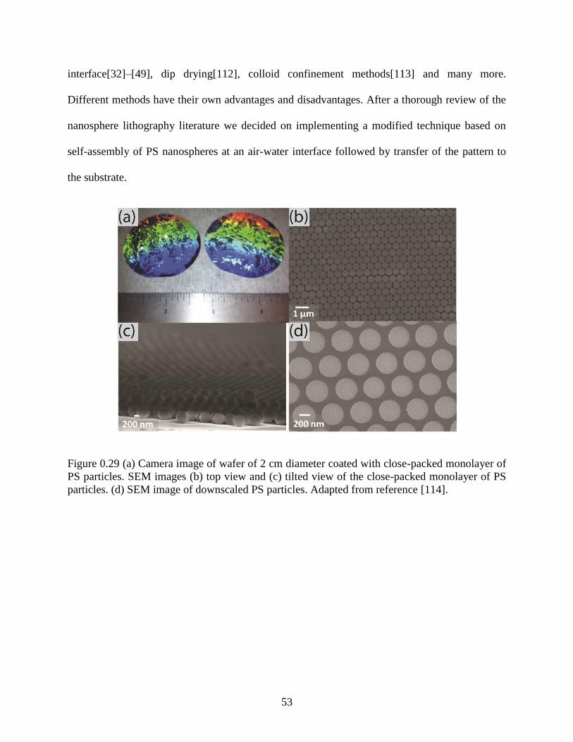
53
interface[32]–[49], dip drying[112], colloid confinement methods[113] and many more.
Different methods have their own advantages and disadvantages. After a thorough review of the
nanosphere lithography literature we decided on implementing a modified technique based on
self-assembly of PS nanospheres at an air-water interface followed by transfer of the pattern to
the substrate.
Figure 0.29 (a) Camera image of wafer of 2 cm diameter coated with close-packed monolayer of
PS particles. SEM images (b) top view and (c) tilted view of the close-packed monolayer of PS
particles. (d) SEM image of downscaled PS particles. Adapted from reference [114].
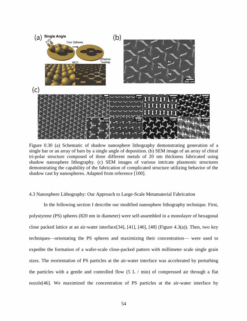
54
Figure 0.30 (a) Schematic of shadow nanosphere lithography demonstrating generation of a
single bar or an array of bars by a single angle of deposition. (b) SEM image of an array of chiral
tri-polar structure composed of three different metals of 20 nm thickness fabricated using
shadow nanosphere lithography. (c) SEM images of various intricate plasmonic structures
demonstrating the capability of the fabrication of complicated structure utilizing behavior of the
shadow cast by nanospheres. Adapted from reference [100].
4.3 Nanosphere Lithography: Our Approach to Large-Scale Metamaterial Fabrication
In the following section I describe our modified nanosphere lithography technique. First,
polystyrene (PS) spheres (820 nm in diameter) were self-assembled in a monolayer of hexagonal
close packed lattice at an air-water interface[34], [41], [46], [48] (Figure 4.3(a)). Then, two key
techniques—orientating the PS spheres and maximizing their concentration— were used to
expedite the formation of a wafer-scale close-packed pattern with millimeter scale single grain
sizes. The reorientation of PS particles at the air-water interface was accelerated by perturbing
the particles with a gentle and controlled flow (5 L / min) of compressed air through a flat
nozzle[46]. We maximized the concentration of PS particles at the air-water interface by
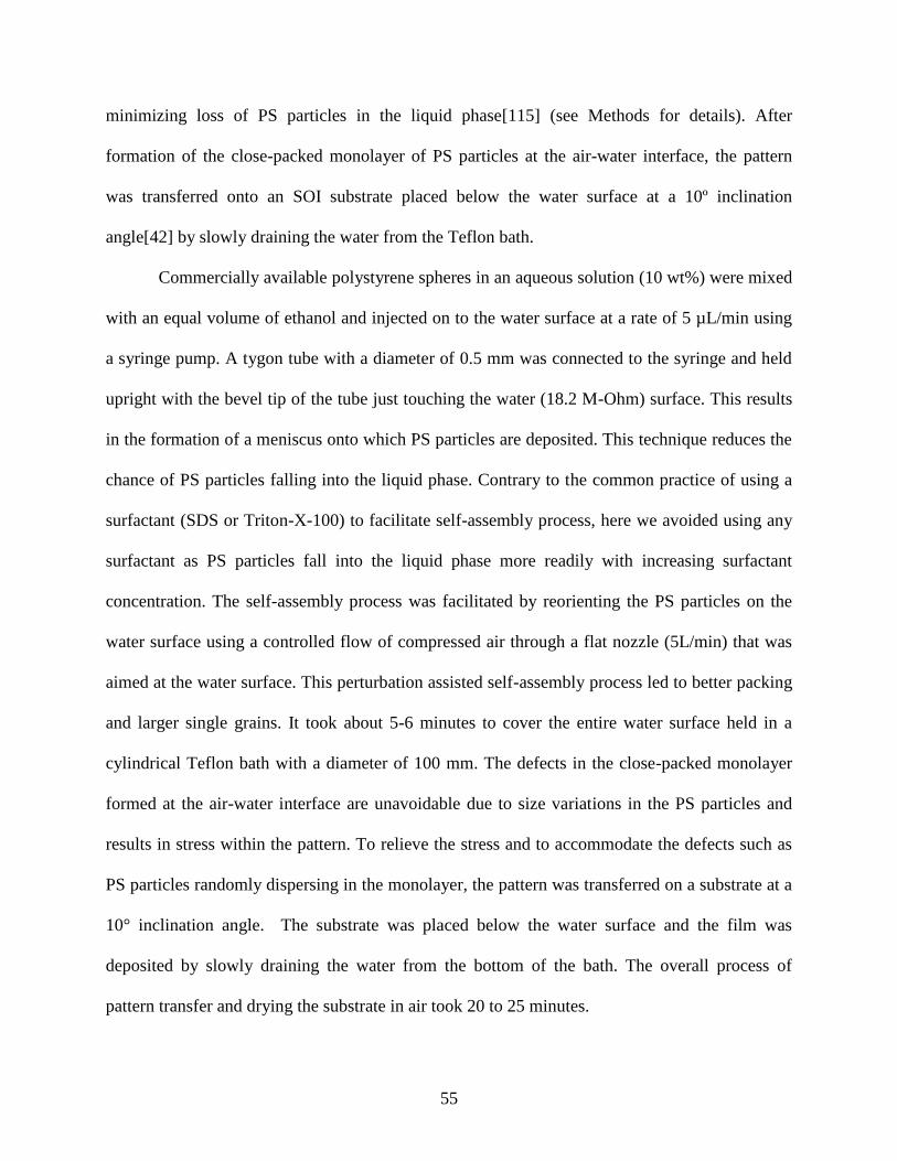
55
minimizing loss of PS particles in the liquid phase[115] (see Methods for details). After
formation of the close-packed monolayer of PS particles at the air-water interface, the pattern
was transferred onto an SOI substrate placed below the water surface at a 10º inclination
angle[42] by slowly draining the water from the Teflon bath.
Commercially available polystyrene spheres in an aqueous solution (10 wt%) were mixed
with an equal volume of ethanol and injected on to the water surface at a rate of 5 µL/min using
a syringe pump. A tygon tube with a diameter of 0.5 mm was connected to the syringe and held
upright with the bevel tip of the tube just touching the water (18.2 M-Ohm) surface. This results
in the formation of a meniscus onto which PS particles are deposited. This technique reduces the
chance of PS particles falling into the liquid phase. Contrary to the common practice of using a
surfactant (SDS or Triton-X-100) to facilitate self-assembly process, here we avoided using any
surfactant as PS particles fall into the liquid phase more readily with increasing surfactant
concentration. The self-assembly process was facilitated by reorienting the PS particles on the
water surface using a controlled flow of compressed air through a flat nozzle (5L/min) that was
aimed at the water surface. This perturbation assisted self-assembly process led to better packing
and larger single grains. It took about 5-6 minutes to cover the entire water surface held in a
cylindrical Teflon bath with a diameter of 100 mm. The defects in the close-packed monolayer
formed at the air-water interface are unavoidable due to size variations in the PS particles and
results in stress within the pattern. To relieve the stress and to accommodate the defects such as
PS particles randomly dispersing in the monolayer, the pattern was transferred on a substrate at a
10° inclination angle. The substrate was placed below the water surface and the film was
deposited by slowly draining the water from the bottom of the bath. The overall process of
pattern transfer and drying the substrate in air took 20 to 25 minutes.
56
An image of a PS pattern assembled on an SOI substrate (2 cm-by-2 cm) is shown in
Figure 4.3(b). The strong opalescence indicates the formation of a close-packed pattern with
individual single grain sizes varying from 2 mm to 10 mm. Next, the PS spheres (SEM image in
Figure 4.3(c)) were downscaled in size to 560 nm (Figure 4.3(d)) using isotropic oxygen plasma
etch. This pattern served as an etch mask for the subsequent RIE processing of Si using SF6 /
C4F8 chemistry. Figures 4.3(e,f) show SEM images of the top and isometric views of the final
metamaterial (after removal of PS mask) consisting of Si cylinders (Dtop=480 nm, Dbottom=554
nm, H=335 nm and P=820 nm) arranged in a hexagonal lattice. The SEM images along with the
optical image clearly demonstrate that the nanosphere lithography can yield high quality
dielectric resonators over a large area.

57
Figure 0.31 (a) Schematic of the self-assembly based nanosphere lithography technique. PS
particles are first assembled in a monolayer at an air-water interface. The monolayer is then
transferred to the SOI substrate by slowly draining the water from the bottom of the Teflon bath.
(b) Camera image of the large-scale pattern (~2 cm-by-2 cm) of close-packed polystyrene
spheres on an SOI substrate. Strong opalescence suggests fabrication of a close packed pattern.
The pattern also exhibits formation of large single grains (mm size). (c-f) SEM images of (c)
hexagonal close-packed polystyrene spheres (green, false color) of diameter 820 nm and (d)
polystyrene spheres downscaled in size to 560 nm using isotropic O2 plasma etching. (e) Top
view of the final metamaterial structure consisting of an array of Si cylinders (blue, false color).
The cylinders were formed by using SF6/ C4F8 reactive ion etch chemistry. (f) Tilted view (45°) of the final metamaterial consisting of an array of Si cylinders (blue, false color). The inset
shows an SEM image of a single Si resonator with a top diameter (Dtop), bottom diameter (Dbottom)
and height (H) of 480 nm, 554 nm and 335 nm, respectively. The scale bar for SEM images (c-f)
is 2 μm.
4.4 Experimental Measurements
The size variations in PS spheres (coefficient of variance (CV) ≤ 3 %) and the self-
assembly process resulted in some disorder of the lattice. The positional disorder (4.1 %) was
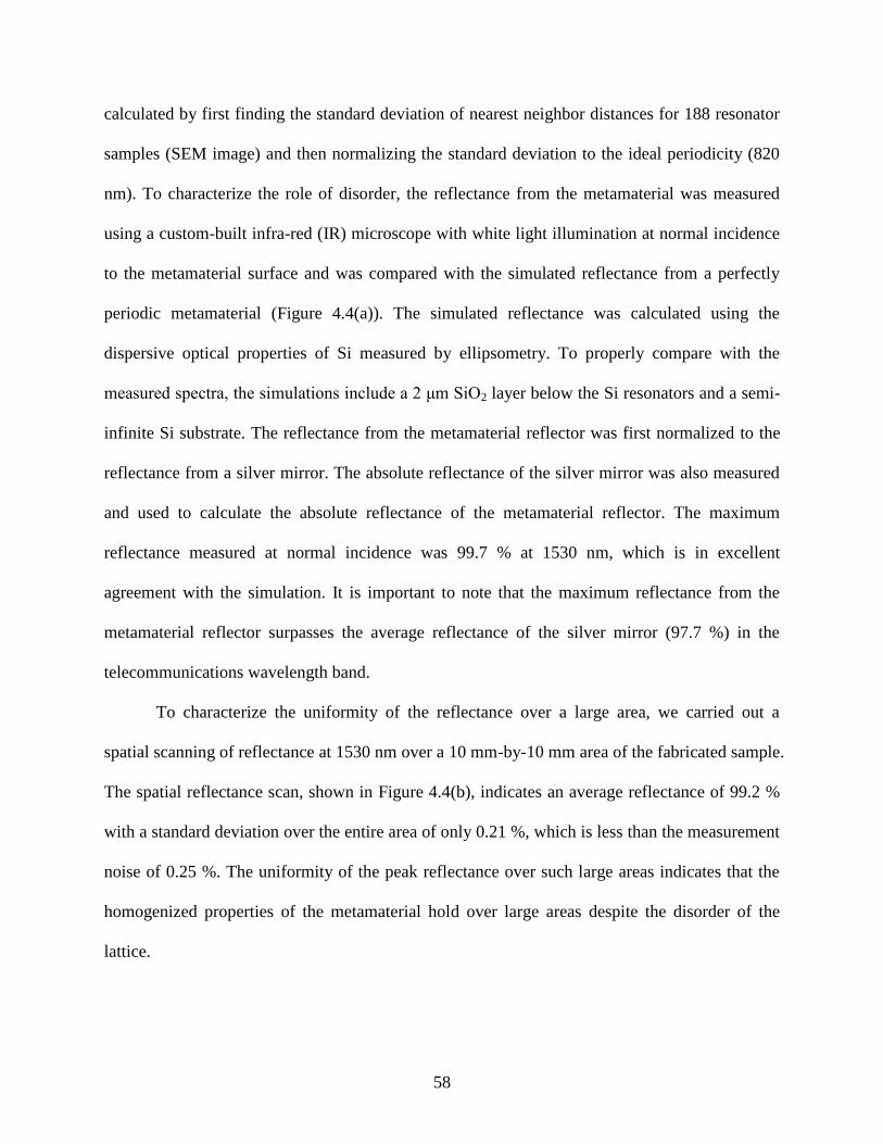
58
calculated by first finding the standard deviation of nearest neighbor distances for 188 resonator
samples (SEM image) and then normalizing the standard deviation to the ideal periodicity (820
nm). To characterize the role of disorder, the reflectance from the metamaterial was measured
using a custom-built infra-red (IR) microscope with white light illumination at normal incidence
to the metamaterial surface and was compared with the simulated reflectance from a perfectly
periodic metamaterial (Figure 4.4(a)). The simulated reflectance was calculated using the
dispersive optical properties of Si measured by ellipsometry. To properly compare with the
measured spectra, the simulations include a 2 μm SiO2 layer below the Si resonators and a semi-
infinite Si substrate. The reflectance from the metamaterial reflector was first normalized to the
reflectance from a silver mirror. The absolute reflectance of the silver mirror was also measured
and used to calculate the absolute reflectance of the metamaterial reflector. The maximum
reflectance measured at normal incidence was 99.7 % at 1530 nm, which is in excellent
agreement with the simulation. It is important to note that the maximum reflectance from the
metamaterial reflector surpasses the average reflectance of the silver mirror (97.7 %) in the
telecommunications wavelength band.
To characterize the uniformity of the reflectance over a large area, we carried out a
spatial scanning of reflectance at 1530 nm over a 10 mm-by-10 mm area of the fabricated sample.
The spatial reflectance scan, shown in Figure 4.4(b), indicates an average reflectance of 99.2 %
with a standard deviation over the entire area of only 0.21 %, which is less than the measurement
noise of 0.25 %. The uniformity of the peak reflectance over such large areas indicates that the
homogenized properties of the metamaterial hold over large areas despite the disorder of the
lattice.
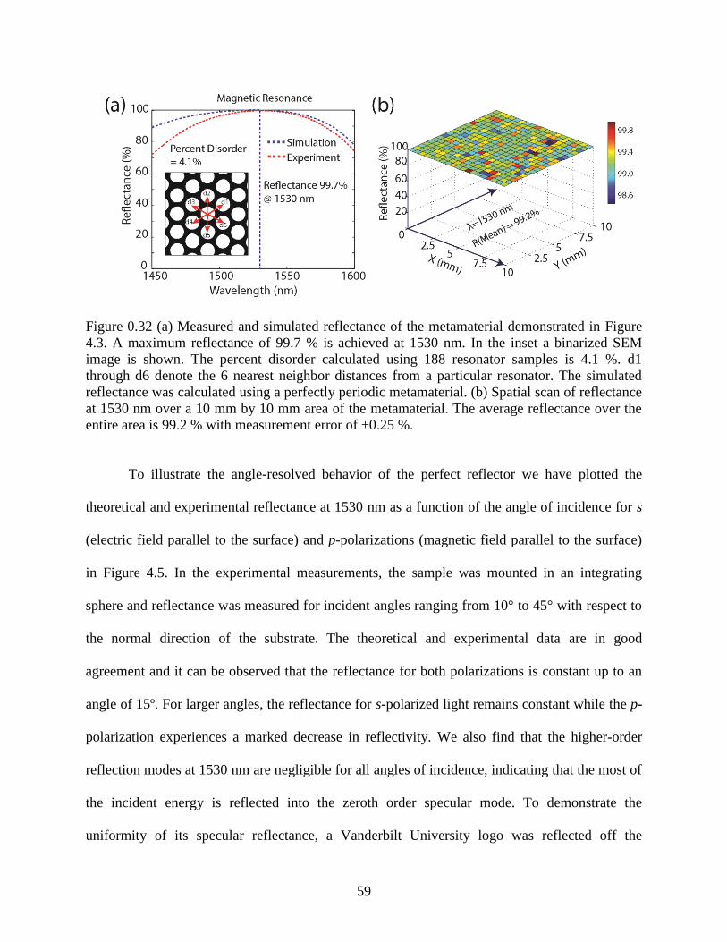
59
Figure 0.32 (a) Measured and simulated reflectance of the metamaterial demonstrated in Figure
4.3. A maximum reflectance of 99.7 % is achieved at 1530 nm. In the inset a binarized SEM
image is shown. The percent disorder calculated using 188 resonator samples is 4.1 %. d1
through d6 denote the 6 nearest neighbor distances from a particular resonator. The simulated
reflectance was calculated using a perfectly periodic metamaterial. (b) Spatial scan of reflectance
at 1530 nm over a 10 mm by 10 mm area of the metamaterial. The average reflectance over the
entire area is 99.2 % with measurement error of ±0.25 %.
To illustrate the angle-resolved behavior of the perfect reflector we have plotted the
theoretical and experimental reflectance at 1530 nm as a function of the angle of incidence for s
(electric field parallel to the surface) and p-polarizations (magnetic field parallel to the surface)
in Figure 4.5. In the experimental measurements, the sample was mounted in an integrating
sphere and reflectance was measured for incident angles ranging from 10° to 45° with respect to
the normal direction of the substrate. The theoretical and experimental data are in good
agreement and it can be observed that the reflectance for both polarizations is constant up to an
angle of 15º. For larger angles, the reflectance for s-polarized light remains constant while the p-
polarization experiences a marked decrease in reflectivity. We also find that the higher-order
reflection modes at 1530 nm are negligible for all angles of incidence, indicating that the most of
the incident energy is reflected into the zeroth order specular mode. To demonstrate the
uniformity of its specular reflectance, a Vanderbilt University logo was reflected off the
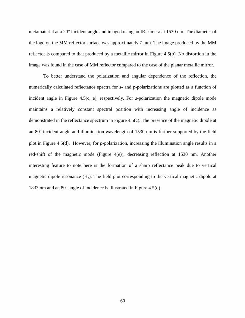
60
metamaterial at a 20° incident angle and imaged using an IR camera at 1530 nm. The diameter of
the logo on the MM reflector surface was approximately 7 mm. The image produced by the MM
reflector is compared to that produced by a metallic mirror in Figure 4.5(b). No distortion in the
image was found in the case of MM reflector compared to the case of the planar metallic mirror.
To better understand the polarization and angular dependence of the reflection, the
numerically calculated reflectance spectra for s- and p-polarizations are plotted as a function of
incident angle in Figure 4.5(c, e), respectively. For s-polarization the magnetic dipole mode
maintains a relatively constant spectral position with increasing angle of incidence as
demonstrated in the reflectance spectrum in Figure 4.5(c). The presence of the magnetic dipole at
an 80° incident angle and illumination wavelength of 1530 nm is further supported by the field
plot in Figure 4.5(d). However, for p-polarization, increasing the illumination angle results in a
red-shift of the magnetic mode (Figure 4(e)), decreasing reflection at 1530 nm. Another
interesting feature to note here is the formation of a sharp reflectance peak due to vertical
magnetic dipole resonance (Hz). The field plot corresponding to the vertical magnetic dipole at
1833 nm and an 80° angle of incidence is illustrated in Figure 4.5(d).
61
Figure 0.33 (a) Schematic of s and p-polarized incident light and the simulated and
experimentally measured angle-resolved reflectances at 1530 nm. Reflectance was measured for
incident angles between 10° and 45°. (b) IR camera images of a Vanderbilt logo that was
reflected off of the MM reflector and a silver mirror with a 20 degree angle of incidence. The
MM reflector leads to strong specular reflectance. The beam diameter at the surfaces of the
reflectors was ~7 mm. (c) Simulated angle-resolved specular reflectances for s-polarized light at
20°, 40°, 60° and 80° angle of incidence. (d) Magnetic field plots (Hy and Hz) illustrating
magnetic dipole resonances. (e) Simulated angle-resolved specular reflectances for p-polarized
light at 20°, 40°, 60° and 80° angles of incidence.
It is also critical to understand what role disorder plays on the electric and magnetic
resonances of the surface. Figure 4.6(a) compares the measured reflectance from a MM with a
disorder of approximately 4 % and the simulated reflectance from a perfectly periodic
metamaterial with a hexagonal lattice (P=820 nm). While the measured reflectance shows
excellent agreement with the simulated reflectance at the magnetic resonance, it is approximately
62
15 % less than the simulated reflectance at the electric resonance. This is because the electric
mode is leaking into the regions between the resonators, whereas the magnetic mode is well
confined within the resonator. To achieve tolerance to disorder, the electric mode must be more
confined inside the resonator which can be achieved by increasing the aspect ratio. In Figure
4.6(b) we present the simulated and measured reflectance from a metamaterial with a resonator
height of 500 nm, increased from 335 nm in the original design. The new design has a 200 nm
broad reflectance band centered at 1700 nm with an average measured reflectance greater than
98 %. The simulated electric field plot shows better confinement for the electric mode inside the
resonators (Dtop=460 nm, Dbottom=600 nm, H=500 nm, P=820 nm) than that observed in Figure
4.6(a) which ultimately results in higher reflectance near the electric mode in the fabricated
samples.
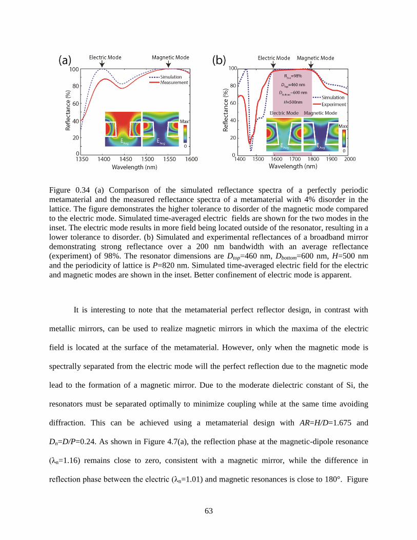
63
Figure 0.34 (a) Comparison of the simulated reflectance spectra of a perfectly periodic
metamaterial and the measured reflectance spectra of a metamaterial with 4% disorder in the
lattice. The figure demonstrates the higher tolerance to disorder of the magnetic mode compared
to the electric mode. Simulated time-averaged electric fields are shown for the two modes in the
inset. The electric mode results in more field being located outside of the resonator, resulting in a
lower tolerance to disorder. (b) Simulated and experimental reflectances of a broadband mirror
demonstrating strong reflectance over a 200 nm bandwidth with an average reflectance
(experiment) of 98%. The resonator dimensions are Dtop=460 nm, Dbottom=600 nm, H=500 nm
and the periodicity of lattice is P=820 nm. Simulated time-averaged electric field for the electric
and magnetic modes are shown in the inset. Better confinement of electric mode is apparent.
It is interesting to note that the metamaterial perfect reflector design, in contrast with
metallic mirrors, can be used to realize magnetic mirrors in which the maxima of the electric
field is located at the surface of the metamaterial. However, only when the magnetic mode is
spectrally separated from the electric mode will the perfect reflection due to the magnetic mode
lead to the formation of a magnetic mirror. Due to the moderate dielectric constant of Si, the
resonators must be separated optimally to minimize coupling while at the same time avoiding
diffraction. This can be achieved using a metamaterial design with AR=H/D=1.675 and
Dn=D/P=0.24. As shown in Figure 4.7(a), the reflection phase at the magnetic-dipole resonance
(λn=1.16) remains close to zero, consistent with a magnetic mirror, while the difference in
reflection phase between the electric (λn=1.01) and magnetic resonances is close to 180°. Figure
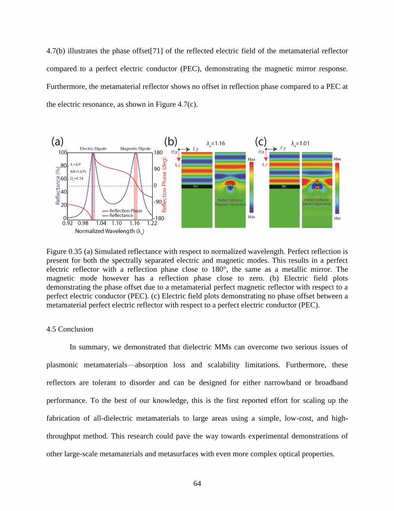
64
4.7(b) illustrates the phase offset[71] of the reflected electric field of the metamaterial reflector
compared to a perfect electric conductor (PEC), demonstrating the magnetic mirror response.
Furthermore, the metamaterial reflector shows no offset in reflection phase compared to a PEC at
the electric resonance, as shown in Figure 4.7(c).
Figure 0.35 (a) Simulated reflectance with respect to normalized wavelength. Perfect reflection is
present for both the spectrally separated electric and magnetic modes. This results in a perfect
electric reflector with a reflection phase close to 180°, the same as a metallic mirror. The
magnetic mode however has a reflection phase close to zero. (b) Electric field plots
demonstrating the phase offset due to a metamaterial perfect magnetic reflector with respect to a
perfect electric conductor (PEC). (c) Electric field plots demonstrating no phase offset between a
metamaterial perfect electric reflector with respect to a perfect electric conductor (PEC).
4.5 Conclusion
In summary, we demonstrated that dielectric MMs can overcome two serious issues of
plasmonic metamaterials—absorption loss and scalability limitations. Furthermore, these
reflectors are tolerant to disorder and can be designed for either narrowband or broadband
performance. To the best of our knowledge, this is the first reported effort for scaling up the
fabrication of all-dielectric metamaterials to large areas using a simple, low-cost, and high-
throughput method. This research could pave the way towards experimental demonstrations of
other large-scale metamaterials and metasurfaces with even more complex optical properties.
65
Chapter 5
Large-Scale Gradient Metasurface Using Nanospherical Lens Lithography: A Perspective of
Advanced Large Scale Lithography with Spatial Control of Patterns
5.1 Introduction
Self-assembly based nanosphere lithography has been proven to be a low cost and high
throughput patterning technique for large area patterning of materials. In Chapter 4, we have
extensively studied and demonstrated large scale fabrication of dielectric metamaterials using
nanosphere lithography. While the technique is restricted to the fabrication of circular patterns,
asymmetric patterns such as ellipses can be generated using a more advanced nanosphere
lithography technique commonly known as nanospherical lens lithography or nanosphere
photolithography[116]–[118]. Here, we take advantage of nanospherical lens lithography, which
utilizes light-focusing through the nanospheres to expose the underlying photoresist, to further
develop a novel large scale gradient lithography technique allowing spatial control over the
orientation of asymmetric patterns.
5.2 Nanosphere Lens Lithography: Past Achievements
In order to illustrate the large scale gradient lithography technique we have to first
understand how basic nanospherical lens lithography works. Nanospherical lens lithography or
nanosphere photolithography is a novel photolithography technique that utilizes a self-assembled
planar array of spheres as optical lenses to generate regular hole-patterns over large areas on a
photoresist. Figure 5.1 shows the basic process flow of nanosphere photolithography. First, a thin
photoresist film is spin coated on the substrate (Figure 5.1(a)) and soft baked at 95° C.
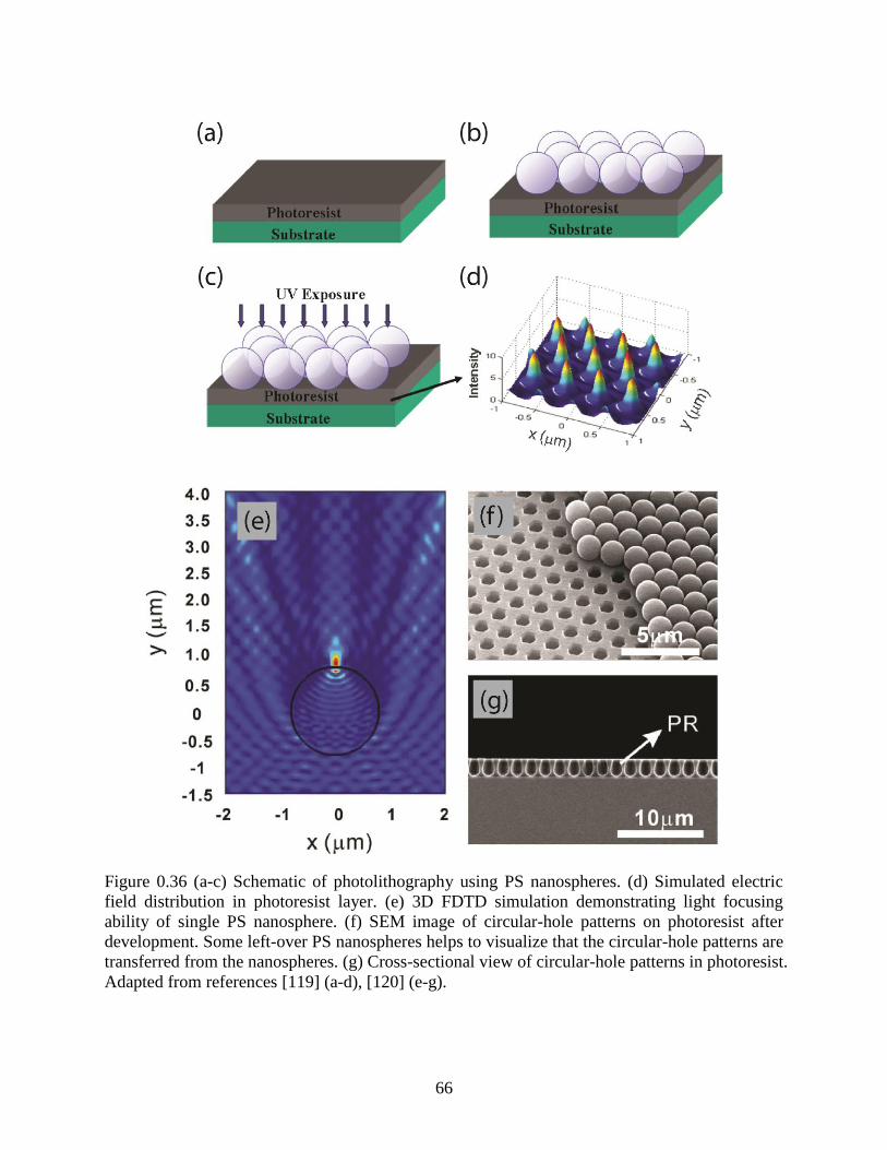
66
Figure 0.36 (a-c) Schematic of photolithography using PS nanospheres. (d) Simulated electric
field distribution in photoresist layer. (e) 3D FDTD simulation demonstrating light focusing
ability of single PS nanosphere. (f) SEM image of circular-hole patterns on photoresist after
development. Some left-over PS nanospheres helps to visualize that the circular-hole patterns are
transferred from the nanospheres. (g) Cross-sectional view of circular-hole patterns in photoresist.
Adapted from references [119] (a-d), [120] (e-g).
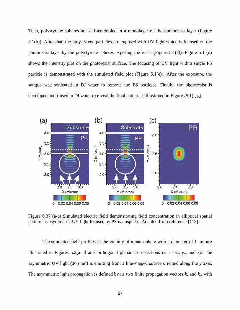
67
Then, polystyrene spheres are self-assembled in a monolayer on the photoresist layer (Figure
5.1(b)). After that, the polystyrene particles are exposed with UV light which is focused on the
photoresist layer by the polystyrene spheres exposing the resist (Figure 5.1(c)). Figure 5.1 (d)
shows the intensity plot on the photoresist surface. The focusing of UV light with a single PS
particle is demonstrated with the simulated field plot (Figure 5.1(e)). After the exposure, the
sample was sonicated in DI water to remove the PS particles. Finally, the photoresist is
developed and rinsed in DI water to reveal the final pattern as illustrated in Figures 5.1(f, g).
Figure 0.37 (a-c) Simulated electric field demonstrating field concentration in elliptical spatial
pattern as asymmetric UV light focused by PS nanosphere. Adapted from reference [118].
The simulated field profiles in the vicinity of a nanosphere with a diameter of 1 μm are
illustrated in Figures 5.2(a–c) at 3 orthogonal planar cross-sections i.e. at xz, yz, and xy. The
asymmetric UV light (365 nm) is emitting from a line-shaped source oriented along the y axis.
The asymmetric light propagation is defined by its two finite propagation vectors kx and kz, with
68
ky=0 (Figures 5.2(a, b)), i.e. propagation vector along the axis of the line source is zero. This
asymmetry in the in-plane wave vector causes asymmetry in focusing of light by the nanospheres.
Because of the finite wave vector along x direction (finite kx and hence divergent beam) light is
more tightly focused along x compared to y direction (as ky=0) and it generates asymmetric or
elliptical focusing spot size in xy plane (Figure 5.2(c)).
Figures 5.3(a-d) illustrate SEM images at different stages of the lithography. Figure 5.3(a)
illustrates SEM images of PS nanospheres assembled on the photoresist layer. The SEM image
of elliptical-hole pattern is demonstrated in Figure 5.3(b). The SEM images of final structures
with two different orientations of the metal nanorods (after metal deposition and lift-off) are
shown in Figures 5.3(c, d).

69
Figure 0.38 SEM images at different steps of lithography to generate elliptical patterns. (a) Self-
assembled close-packed nanospheres. (b) Elliptical-hole patterns in photoresist after lift-off. (c,d)
metal nanorods after lift-off, oriented differently. Adapted from reference [118].
5.3 Large-Scale Metasurface Using Modified and Advanced Nanospherical Lens Lithography
5.3.1 Optical Set Up for Lithography
With this basic understanding of nanospherical lens lithography, here we describe our
approach to modify the basic nanospherical lens lithography to further develop large scale
gradient metasurfaces. Figure 5.4(a) demonstrates the schematic of the optical set-up for the
exposure. A CW Nitrogen (N2) laser (405 nm) is used as the light source. The 405 nm laser light
first goes through a 50:50 non-polarizing cube beam splitter and is reflected off of a digital
micro-mirror device (DMD), which imparts a desired spatial pattern in the reflected light with
this pattern being imaged at the sample. Here, it is important to note that spatial patterning of

70
light is important to define a particular region in the sample having a particular orientation of the
elliptical pattern. The spatially patterned light (Figure 5.4 (b)) is again reflected from the beam
splitter. The orientation of the ellipse is controlled by masking the Fourier plane with a
rectangular slit. The rectangular slit transmits all the k-vectors along the length of the slit, while
suppresses the high k-vectors in the direction of the short axis. All the higher order diffracted
modes from the micro-mirror array are also masked at the Fourier plane. The transmitted light,
which is masked at the Fourier plane, defines the asymmetric illumination that is incident on the
monolayer of nanospheres and in turn is focused asymmetrically by the PS particles to generate
the elliptical-hole pattern in the underlying photoresist. It is important to note here that the
orientation of the patterned ellipse is normal to the slit axis (Figure 5.5(c)). To define different
regions on the sample with different orientations of ellipses the spatial patterning of the light is is
accompanied by rotating the axis of the slit which is mounted on a rotation stage.
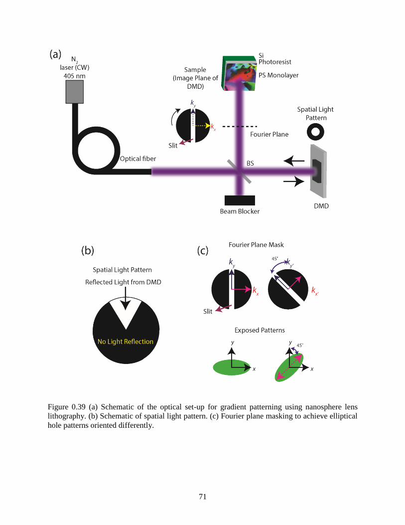
71
Figure 0.39 (a) Schematic of the optical set-up for gradient patterning using nanosphere lens
lithography. (b) Schematic of spatial light pattern. (c) Fourier plane masking to achieve elliptical
hole patterns oriented differently.
72
5.4 Motivation: Metasurfaces
The motivation behind developing the advanced nanosphere photolithography technique
is to achieve low cost and high throughput fabrication of metasurfaces that are composed of
spatially varying resonators. ‘Metasurfaces’ are planar ultra-thin optical components that provide
complete control over the phase of light, opposed to conventional optical elements that solely
depend on accumulating phase during propagation over an optical path that is much larger than
the wavelength. With complete control of light i.e., spatial phase variation from 0 to 2π,
metasurfaces provide a new design methodology that can be used to realize novel ultra-thin
optics such as ultrathin planar lenses[121], [122], optical vortex beam generation[123], [124] and
holograms[125]–[127]. Metasurfaces typically utilize asymmetric electric dipole resonances to
allow 0 to 2π phase control for the cross-polarized light. Initial metasurface work started by
utilizing plasmonic antennae, however, one of the drawbacks of plasmonic metasurfaces is that
they generally suffer from low efficiency because of weak coupling between incident and cross-
polarized fields. In order to increase efficiency, efforts have been made to combine an array of
plasmonic nano antennae with a metal ground plane to achieve 80% efficiency for anomalous
reflection and linear polarization conversion. However, the use of metallic nano antennae still
limits the efficiency because of ohmic loss at optical frequencies. The efficiency for polarization
conversion was recently boosted up to 98% over a 200 nm bandwidth in the short infrared band
by replacing metallic nano antennas with dielectric nano antennas. This allowed high efficiency
optical vortex beam generation over a band from 1500-1600 nm by azimuthally varying the
phase of the cross polarized reflected light[65]. Some selected examples of metasurfaces are
demonstrated in Figure 5.6.
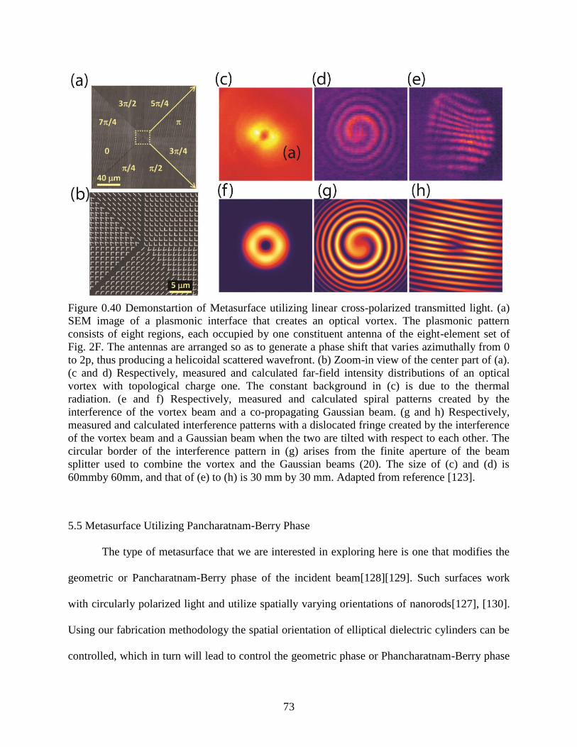
73
Figure 0.40 Demonstartion of Metasurface utilizing linear cross-polarized transmitted light. (a)
SEM image of a plasmonic interface that creates an optical vortex. The plasmonic pattern
consists of eight regions, each occupied by one constituent antenna of the eight-element set of
Fig. 2F. The antennas are arranged so as to generate a phase shift that varies azimuthally from 0
to 2p, thus producing a helicoidal scattered wavefront. (b) Zoom-in view of the center part of (a).
(c and d) Respectively, measured and calculated far-field intensity distributions of an optical
vortex with topological charge one. The constant background in (c) is due to the thermal
radiation. (e and f) Respectively, measured and calculated spiral patterns created by the
interference of the vortex beam and a co-propagating Gaussian beam. (g and h) Respectively,
measured and calculated interference patterns with a dislocated fringe created by the interference
of the vortex beam and a Gaussian beam when the two are tilted with respect to each other. The
circular border of the interference pattern in (g) arises from the finite aperture of the beam
splitter used to combine the vortex and the Gaussian beams (20). The size of (c) and (d) is
60mmby 60mm, and that of (e) to (h) is 30 mm by 30 mm. Adapted from reference [123].
5.5 Metasurface Utilizing Pancharatnam-Berry Phase
The type of metasurface that we are interested in exploring here is one that modifies the
geometric or Pancharatnam-Berry phase of the incident beam[128][129]. Such surfaces work
with circularly polarized light and utilize spatially varying orientations of nanorods[127], [130].
Using our fabrication methodology the spatial orientation of elliptical dielectric cylinders can be
controlled, which in turn will lead to control the geometric phase or Phancharatnam-Berry phase
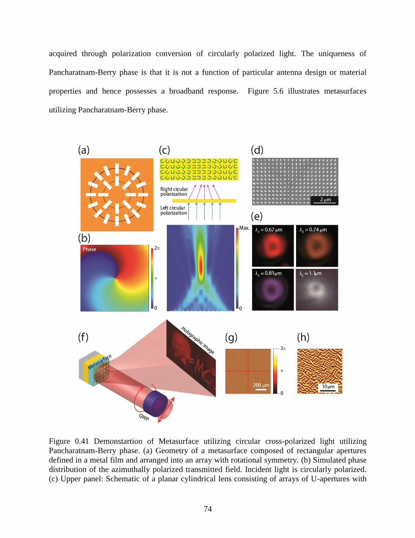
74
acquired through polarization conversion of circularly polarized light. The uniqueness of
Pancharatnam-Berry phase is that it is not a function of particular antenna design or material
properties and hence possesses a broadband response. Figure 5.6 illustrates metasurfaces
utilizing Pancharatnam-Berry phase.
Figure 0.41 Demonstartion of Metasurface utilizing circular cross-polarized light utilizing
Pancharatnam-Berry phase. (a) Geometry of a metasurface composed of rectangular apertures
defined in a metal film and arranged into an array with rotational symmetry. (b) Simulated phase
distribution of the azimuthally polarized transmitted field. Incident light is circularly polarized.
(c) Upper panel: Schematic of a planar cylindrical lens consisting of arrays of U-apertures with
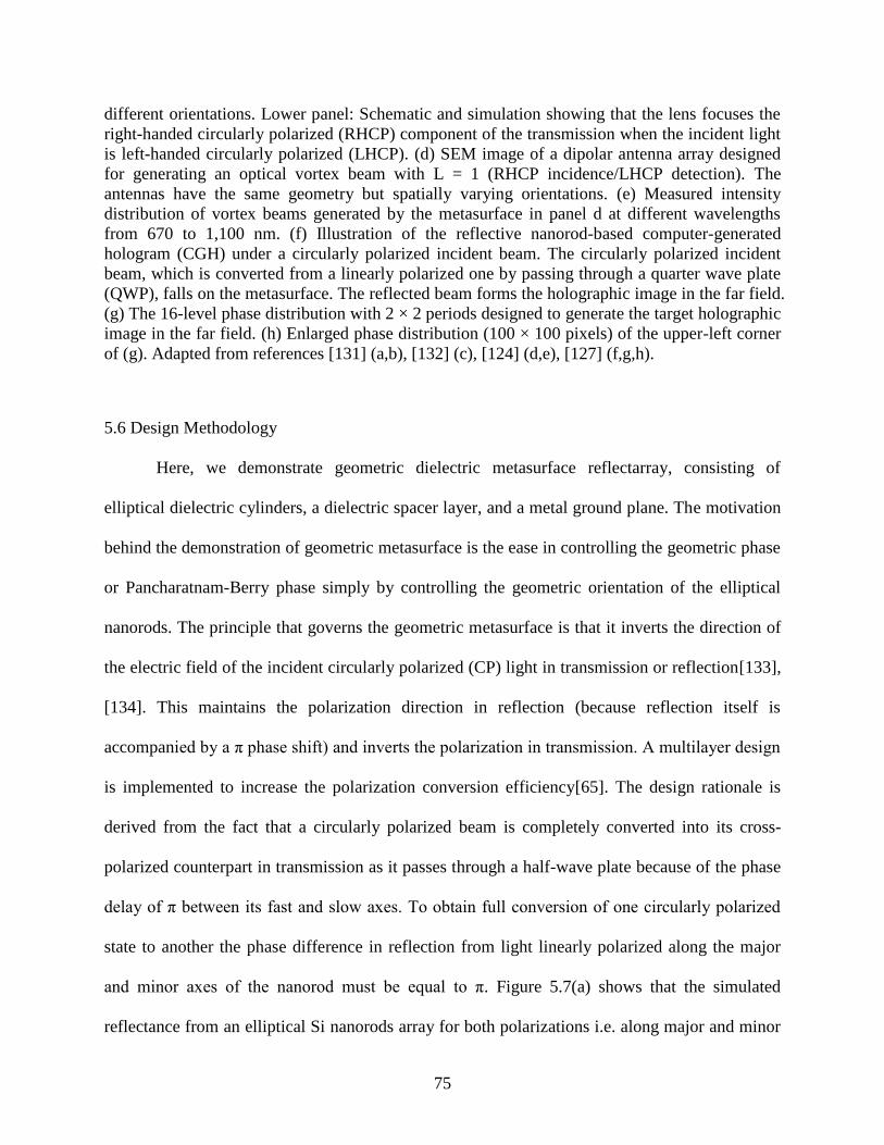
75
different orientations. Lower panel: Schematic and simulation showing that the lens focuses the
right-handed circularly polarized (RHCP) component of the transmission when the incident light
is left-handed circularly polarized (LHCP). (d) SEM image of a dipolar antenna array designed
for generating an optical vortex beam with L = 1 (RHCP incidence/LHCP detection). The
antennas have the same geometry but spatially varying orientations. (e) Measured intensity
distribution of vortex beams generated by the metasurface in panel d at different wavelengths
from 670 to 1,100 nm. (f) Illustration of the reflective nanorod-based computer-generated
hologram (CGH) under a circularly polarized incident beam. The circularly polarized incident
beam, which is converted from a linearly polarized one by passing through a quarter wave plate
(QWP), falls on the metasurface. The reflected beam forms the holographic image in the far field.
(g) The 16-level phase distribution with 2 × 2 periods designed to generate the target holographic
image in the far field. (h) Enlarged phase distribution (100 × 100 pixels) of the upper-left corner
of (g). Adapted from references [131] (a,b), [132] (c), [124] (d,e), [127] (f,g,h).
5.6 Design Methodology
Here, we demonstrate geometric dielectric metasurface reflectarray, consisting of
elliptical dielectric cylinders, a dielectric spacer layer, and a metal ground plane. The motivation
behind the demonstration of geometric metasurface is the ease in controlling the geometric phase
or Pancharatnam-Berry phase simply by controlling the geometric orientation of the elliptical
nanorods. The principle that governs the geometric metasurface is that it inverts the direction of
the electric field of the incident circularly polarized (CP) light in transmission or reflection[133],
[134]. This maintains the polarization direction in reflection (because reflection itself is
accompanied by a π phase shift) and inverts the polarization in transmission. A multilayer design
is implemented to increase the polarization conversion efficiency[65]. The design rationale is
derived from the fact that a circularly polarized beam is completely converted into its cross-
polarized counterpart in transmission as it passes through a half-wave plate because of the phase
delay of π between its fast and slow axes. To obtain full conversion of one circularly polarized
state to another the phase difference in reflection from light linearly polarized along the major
and minor axes of the nanorod must be equal to π. Figure 5.7(a) shows that the simulated
reflectance from an elliptical Si nanorods array for both polarizations i.e. along major and minor
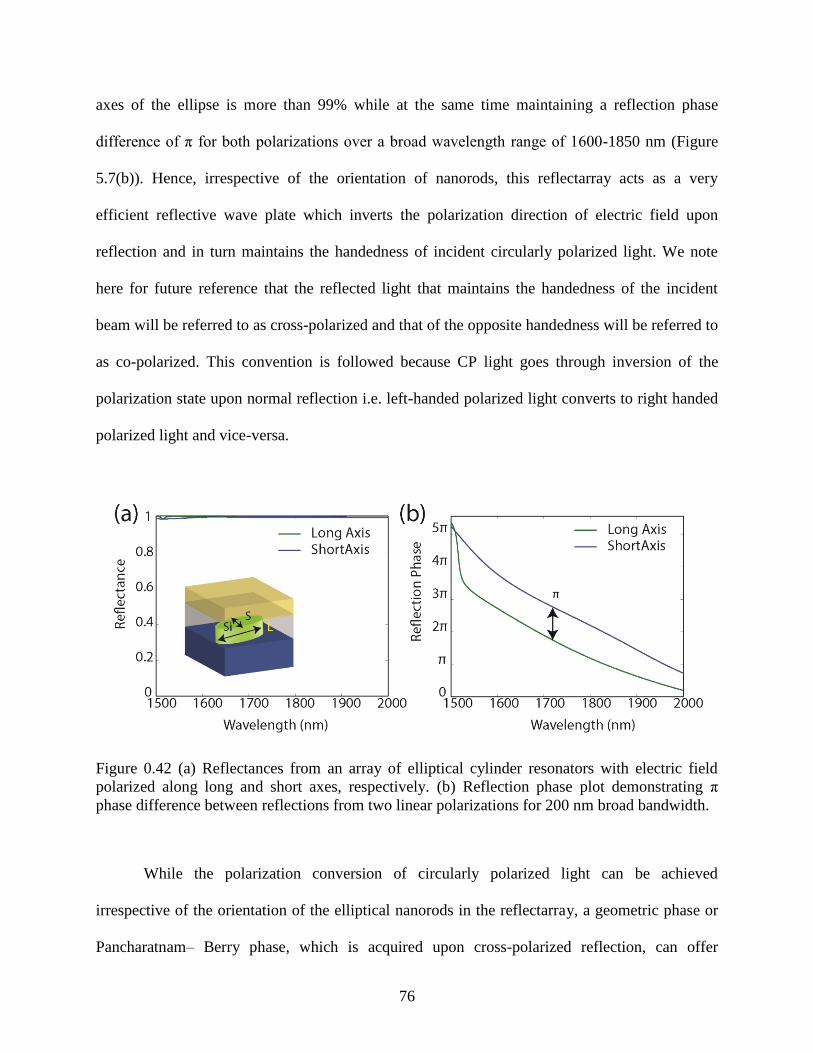
76
axes of the ellipse is more than 99% while at the same time maintaining a reflection phase
difference of π for both polarizations over a broad wavelength range of 1600-1850 nm (Figure
5.7(b)). Hence, irrespective of the orientation of nanorods, this reflectarray acts as a very
efficient reflective wave plate which inverts the polarization direction of electric field upon
reflection and in turn maintains the handedness of incident circularly polarized light. We note
here for future reference that the reflected light that maintains the handedness of the incident
beam will be referred to as cross-polarized and that of the opposite handedness will be referred to
as co-polarized. This convention is followed because CP light goes through inversion of the
polarization state upon normal reflection i.e. left-handed polarized light converts to right handed
polarized light and vice-versa.
Figure 0.42 (a) Reflectances from an array of elliptical cylinder resonators with electric field
polarized along long and short axes, respectively. (b) Reflection phase plot demonstrating π
phase difference between reflections from two linear polarizations for 200 nm broad bandwidth.
While the polarization conversion of circularly polarized light can be achieved
irrespective of the orientation of the elliptical nanorods in the reflectarray, a geometric phase or
Pancharatnam– Berry phase, which is acquired upon cross-polarized reflection, can offer
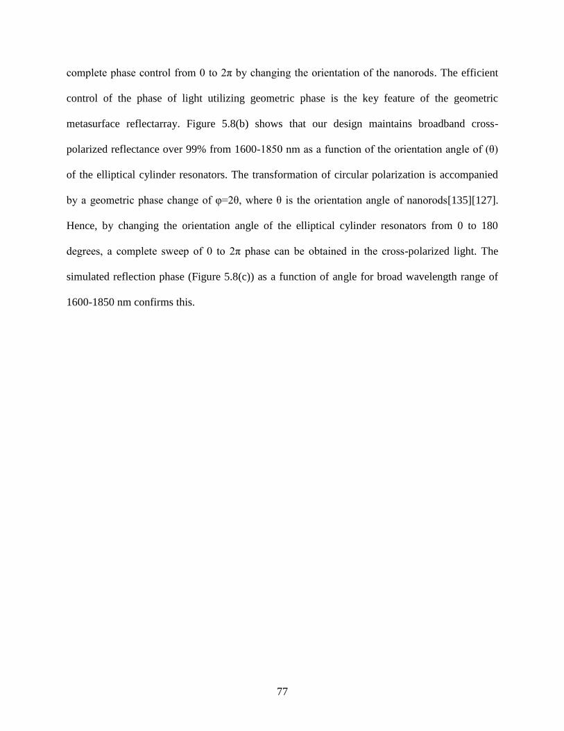
77
complete phase control from 0 to 2π by changing the orientation of the nanorods. The efficient
control of the phase of light utilizing geometric phase is the key feature of the geometric
metasurface reflectarray. Figure 5.8(b) shows that our design maintains broadband cross-
polarized reflectance over 99% from 1600-1850 nm as a function of the orientation angle of (θ)
of the elliptical cylinder resonators. The transformation of circular polarization is accompanied
by a geometric phase change of φ=2θ, where θ is the orientation angle of nanorods[135][127].
Hence, by changing the orientation angle of the elliptical cylinder resonators from 0 to 180
degrees, a complete sweep of 0 to 2π phase can be obtained in the cross-polarized light. The
simulated reflection phase (Figure 5.8(c)) as a function of angle for broad wavelength range of
1600-1850 nm confirms this.
78
Figure 0.43 (a) Schematic of elliptical patterns with different orientations. (b) Broadband cross-
polarized reflectance as a function of orientation of resonators. (c) Broadband cross-polarized
reflection phase as a function of orientation of resonators. Complete phase control from 0 to 2π is
demonstrated for over 200 nm bandwidth. (d,e) Phase profiles for optical vortex generator and
axicon, respectively.
79
5.7 Practical Implementation
The first step in the fabrication of an asymmetric dielectric meta-reflectarray is the
deposition of 400 nm of high density amorphous Si on quartz substrate using low pressure
chemical vapor deposition (LPCVD) furnace. The substrate is then diced to 20mm X 20 mm
sized samples. The sample is spin-coated at 6000 rpm with diluted AZ5214 photoresist which is
diluted with equal volume of solvent (AZ EBR) to get 500 nm thin photoresist layer. The
photoresist is soft baked at 95° C and immersed in MIF 316 solution to provide hydrophilicity to
the surface, which helps in the self-assembly of PS monolayer on the photoresist film. The same
procedure as described in the previous chapter is used in the process of self-assembly and pattern
transfer on the substrate. AZ5214 is sensitive to both i-(~365 nm) and h-line (~405 nm) exposure.
Here, we utilize the h-line exposure (405 nm) because of the optimized working wavelength of
400-700 nm for the DMD and also for the availability of laser source. After the exposure, the
polystyrene particles are removed by sonication of the sample in DI water. The photoresist is
developed with MIF 316 developer which reveals the elliptical-hole arrays.
The remainder of the fabrication follows the conventional lift-off process to metallize the
elliptical mask followed by reactive ion etching (RIE) of the underlying silicon. 250 nm PMMA
is then spin-coated on the sample, followed by soft baking (180 degrees for 2 minutes) and
reflowing at 300° C for 2 minutes to reach the desired thickness and flatness. In the last step, 150
nm of silver is thermally deposited on top of the sample, serving as the ground metal plane. The
entire process is summarized in Figure 5.5.
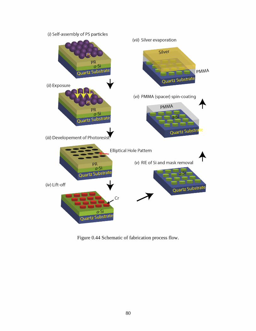
80
Figure 0.44 Schematic of fabrication process flow.
81
5.8 Future Demonstrations
The two most important parameters to create a metasurface are complete 0 to 2π phase
control and efficient conversion of polarization. In our design we have demonstrated over 99%
efficiency in polarization conversion along with complete phase control using a dielectric meta-
reflectarray. With the advanced lithography technique outlined in this chapter the fabrication of
different metasurfaces such as lenses, axicons, optical vortex generators or phase holograms will
be greatly simplified and expedited with at the same time cost of fabrication will be highly
reduced. However, the experimental demonstration of such a metasurface is not within the scope
of this dissertation and will be explored in detail in future work.
5.9 Conclusion
Here, we demonstrated the idea of a novel lithography approach that combines
asymmetric pattern generation with the spatial control of resonator orientation using spatial light
patterning using a DMD. The overall lithography set-up is simple and should result in high
throughput fabrication of metasurfaces. Moreover, in addition to controlling the orientation of
the patterns the size of the pattern can also be controlled spatially by controlling the intensity of
the incident light using grayscale masking. Better control over resonator size can also be
implemented by controlling the Fourier plane masking. We believe that the demonstration of a
simple, low-cost and high-throughput gradient lithography technique will lead to the
implementation of metasurfaces for practical applications.
82
Chapter 6
Conclusion and Future Outlook
6.1 Conclusion
The advent of metamaterial research started with the use of metal based unit cells[1][18]
and many interesting demonstrations have followed including negative index of refraction[25]–
[27], ultra-high index[8], epsilon near zero[5]–[7], [136], electromagnetically induced
transparency[137]–[144], chirality[145]–[148], nonlinearity[149]–[155], magnetic mirrors[97],
and spatial control of phase [72], [123], [125], [127], [156]. However, at optical frequencies the
path towards further improvement using metal based metamaterials face immense challenges
mostly because of parasitic loss due to absorption. Secondly, with scaling to high frequencies
dimensions of the unit cells gets extremely small and the intricate unit cell designs prohibit large
area scalability due to the need for expensive patterning equipment. Thirdly, the intricate unit
cell designs also render the optical properties anisotropic. While metal based designs served well
to understand the physics of metamaterials, the search for alternative approaches is now in full
swing. Dielectric metamaterials are excellent alternatives which address all the challenges faced
by metal based metamaterials. Dielectric materials are lossless at optical frequencies and exhibit
electric and magnetic dipole Mie resonances with very simple and isotropic resonator geometries,
which, in turn, can result in an isotropic optical response. Finally, due to simple resonator
designs dielectric metamaterials offer large area scalability with simple, low cost, and expedited
83
lithography processes. The purpose of my research has been to take advantage of all these
interesting features and hopefully contribute to advancing this field of study.
In Chapter 2, I experimentally demonstrated zero-index-metamaterial with multilayered
design at optical frequencies[81]. A proper design methodology has been followed to achieve
Dirac cone like dispersion in band diagram of a square lattice of dielectric (Si) rods with square
cross section. Effective metamaterial properties have been retrieved to demonstrate impedance
matched zero index of refraction. Rigorous fabrication challenges were overcome to achieve
uniform resonator dimensions in the direction normal to the plane of substrate. Finally, zero
index of refraction was experimentally demonstrated with directional transmission and
directional enhanced emission from quantum dots from inside the ZIM.
In Chapter 3, I explored the advantage of using dielectric (Si) cylinder unit cell as it
offers control over spectral manipulation of electric and magnetic resonances. With optimized
design, I was able to demonstrate broadband perfect reflection from sub-wavelength single layer
metamaterial formed from ordered and disordered arrays of Si cylinders[95][157]. Because of
the simple unit cell design, this research leads to the farther demonstration of perfect reflection
from large area using low cost and high throughput fabrication technique for practical
applications.
In Chapter 4, I scaled the metamaterial perfect reflector to large area (centimeter size). To
fabricate large area metamaterial, I developed a modified nanosphere lithography technique with
self-assembly of polystyrene particles which forms a highly close packed monolayer. The size of
the polystyrene particles is then reduced using isotropic oxygen plasma etching and the
downscaled polystyrene particles are used as mask for subsequent reactive ion etching of silicon.
The influence of disorder in the lattice imparted by the self-assembly process, on reflection was

84
studied at electric and magnetic modes. It was found that reflection at magnetic modes is more
tolerant to that of electric modes. This was because of the fact that magnetic mode is more
confined in the resonators than the electric modes and disorder does not influence the optical
response at magnetic mode. I farther proposed a mechanism and demonstrated that with
increasing aspect ratio the electric mode can also be confined inside the resonators which will
lead to high reflectance at electric mode and can be used to achieve broadband reflectance.
Finally, a design is numerically proposed for achieving magnetic mirror at optical frequencies,
which can be fabricated conveniently in large area with the present capability.
In Chapter 5, the perspective of advancement of nanosphere lithography is discussed
which can lead to achieve gradient metasurface with spatially varying resonator sizes and
orientations. The key to achieve this advanced nanosphere photolithography technique is to first
spatially pattern light using a digital micro-mirror device (DMD) which is imaged at the sample
and second, controlling the wave vector of light at the Fourier plane for asymmetric light
illumination at the sample. Spatial patterned light defines the pixel locations on the sample while
orientation of rectangular slit at the Fourier plane controls the orientation of the elliptical-hole
pattern in the photoresist. The asymmetric light incident leads to asymmetric focal spot on the
photoresist and in turn leads to formation of elliptical-hole pattern.
6.2 Future Outlook
2015 is being celebrated as the International Year of Light. As a researcher in optical
metamaterials I take pride in the contributions that metamaterials research has made in the
advancement of the fields of photonics and plasmonics. Still, there is a long and bumpy road
ahead for metamaterials that requires further research advances. Here, I will briefly describe the
85
major challenges that can be addressed by advancing the future research in the direction of my
dissertation work.
The performance of all-dielectric metamaterials can be greatly improved at
telecommunication wavelengths if the dielectric permittivity of the constituent material is high,
because of stronger and more confined dipole resonances and sub-wavelength unit cell
geometries. Silicon serves as the most suitable material in this wavelength range because of its
comparatively high permittivity ( 12~ε ) and low loss. However, it should be actively pursued
to develop a metamaterial which has low-loss and high effective permittivity,effε (much higher
than ε of silicon). This artificial high permittivity metamaterial with low-loss would serve as an
ideal constituent to further develop a “Meta-Metamaterial” design, i.e. a metamaterial which is
composed of unit cells made of homogeneous metamaterials. Though the idea may sound a little
far-fetched, the motivation can be derived from experimental demonstration of high-permittivity
metamaterials in THz wavelengths[8].
Another interesting area for advancement is the active tunability of silicon based
metamaterial properties at telecommunication wavelengths. This can be achieved with the
thermo-optic and electro-optic effects in silicon i.e. changing index of refraction of silicon as a
function of an increase in temperature[158] or electric field[159]. These effects has been
experimentally demonstrated for silicon based waveguides[160]–[163]. Experimental
demonstration of the tunability of resonances of silicon resonator based dielectric metamaterials
is yet to be done and is subject to future study.
Finally, for practical applications and commercialization of metamaterials, development
of a cost-effective well-ordered large area fabrication with minimum defect is essential.
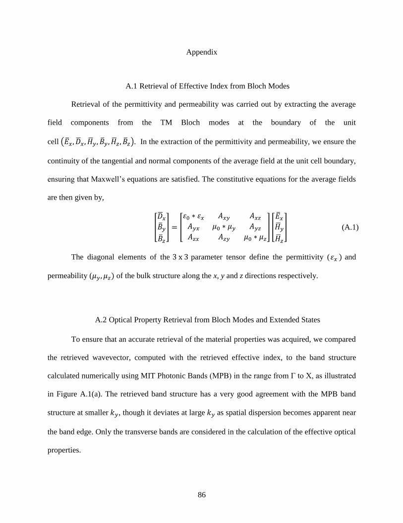
86
Appendix
A.1 Retrieval of Effective Index from Bloch Modes
Retrieval of the permittivity and permeability was carried out by extracting the average
field components from the TM Bloch modes at the boundary of the unit
cell ( 𝑦 𝑦 ). In the extraction of the permittivity and permeability, we ensure the
continuity of the tangential and normal components of the average field at the unit cell boundary,
ensuring that Maxwell’s equations are satisfied. The constitutive equations for the average fields
are then given by,
[
𝑦
] [
𝑦
𝑦 𝑦 𝑦
𝑦
] [
𝑦
] (A.1)
The diagonal elements of the parameter tensor define the permittivity ( and
permeability ( 𝑦 of the bulk structure along the x, y and z directions respectively.
A.2 Optical Property Retrieval from Bloch Modes and Extended States
To ensure that an accurate retrieval of the material properties was acquired, we compared
the retrieved wavevector, computed with the retrieved effective index, to the band structure
calculated numerically using MIT Photonic Bands (MPB) in the range from Γ to Х, as illustrated
in Figure A.1(a). The retrieved band structure has a very good agreement with the MPB band
structure at smaller 𝑦, though it deviates at large 𝑦 as spatial dispersion becomes apparent near
the band edge. Only the transverse bands are considered in the calculation of the effective optical
properties.
87
In order to properly assign a refractive index to a material for off-normal angles of
incidence, there must be only one propagating band at a particular frequency. To verify that there
is only one propagating band within the material, we simulated the extended states of the crystal,
shown in Figure A.1(b). Within the frequency range from 215 THz to 225 THz, slightly above
the zero-index point, there is a single band (TM4) throughout k-space. Within this region, a
refractive index may be assigned to the metamaterial, though it may change slightly with the
angle of incidence, as illustrated in the IFC plot shown in Figure 2.1(c).
Figure A. 1 Comparison of optical properties and band structure and extended states of the
metamaterial. a, The solid lines represent the band structure of the square lattice calculated from
MPB and the circles correspond to band diagram retrieved from effective index and the
dispersion relation 𝑦 ⁄ . The mismatch of the two methods at the band edge is due to
the fact that the effective medium approximation no longer holds in those regions. b, Extended
states of the crystal showing that only one band (TM4) is present between 215 THz and 225 THz,
allowing an effective index to be assigned to this region.
A.3 Comparison of Normal and Angle Dependent Transmission from ZIM and
Homogeneous Media
To verify the use of effective constitutive properties in the case of the ZIM, we also
simulated normal and angle dependent transmission of a homogeneous medium with the same
effective optical properties. The ZIM structure that was simulated consisted of 5 identical unit
cells along the light propagation direction and the homogenous medium it was compared to was
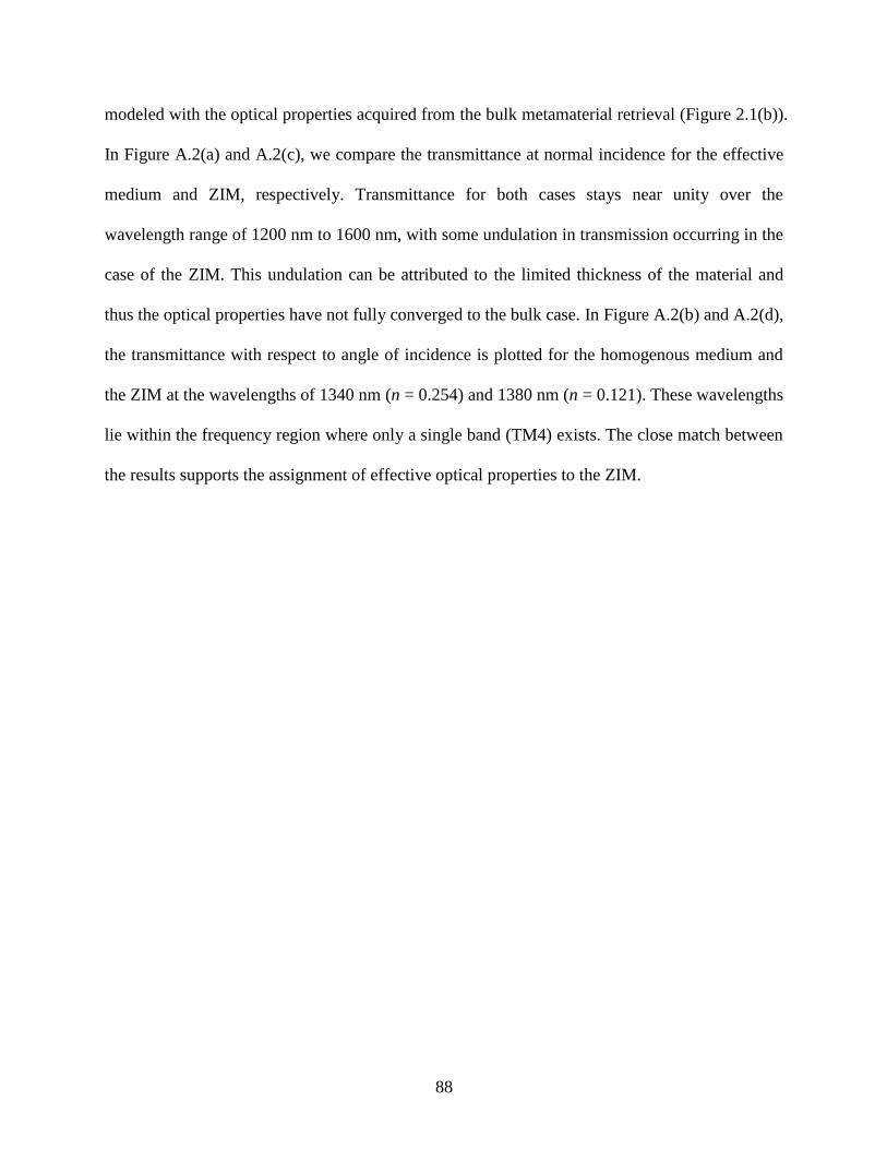
88
modeled with the optical properties acquired from the bulk metamaterial retrieval (Figure 2.1(b)).
In Figure A.2(a) and A.2(c), we compare the transmittance at normal incidence for the effective
medium and ZIM, respectively. Transmittance for both cases stays near unity over the
wavelength range of 1200 nm to 1600 nm, with some undulation in transmission occurring in the
case of the ZIM. This undulation can be attributed to the limited thickness of the material and
thus the optical properties have not fully converged to the bulk case. In Figure A.2(b) and A.2(d),
the transmittance with respect to angle of incidence is plotted for the homogenous medium and
the ZIM at the wavelengths of 1340 nm (n = 0.254) and 1380 nm (n = 0.121). These wavelengths
lie within the frequency region where only a single band (TM4) exists. The close match between
the results supports the assignment of effective optical properties to the ZIM.
89
Figure A. 2 Comparison of normal and angle dependent transmittance of a homogeneous
medium and the ZIM structure. a,c, Transmittance of the homogeneous medium and ZIM
structure (5 periods), respectively, under normal incidence. b,d, Angle dependent transmittance
of the homogeneous medium and ZIM structure, respectively, at wavelengths of 1340 nm and
1380 nm.
A.4 Homogeneous Effective Materials Properties
To further justify our claim that the proposed metamaterial structure can indeed be
homogenized as an effective medium and has an isotropic low index property for TM-polarized
light, we conducted numerical simulation with a Gaussian beam incident at the ZIM from
multiple angles. The wavelengths of the incident beams (1340nm and 1380nm) are chosen such
that they fall within the bandwidth where only one propagating band (TM4) exists.
The simulated electric field profiles with multiple angles of incidence and wavelengths
are shown in Figures A.3(a-f). In all cases, we see no higher order diffraction taking place at the
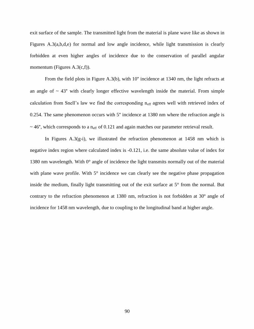
90
exit surface of the sample. The transmitted light from the material is plane wave like as shown in
Figures A.3(a,b,d,e) for normal and low angle incidence, while light transmission is clearly
forbidden at even higher angles of incidence due to the conservation of parallel angular
momentum (Figures A.3(c,f)).
From the field plots in Figure A.3(b), with 10° incidence at 1340 nm, the light refracts at
an angle of ~ 43° with clearly longer effective wavelength inside the material. From simple
calculation from Snell’s law we find the corresponding neff agrees well with retrieved index of
0.254. The same phenomenon occurs with 5° incidence at 1380 nm where the refraction angle is
~ 46°, which corresponds to a neff of 0.121 and again matches our parameter retrieval result.
In Figures A.3(g-i), we illustrated the refraction phenomenon at 1458 nm which is
negative index region where calculated index is -0.121, i.e. the same absolute value of index for
1380 nm wavelength. With 0° angle of incidence the light transmits normally out of the material
with plane wave profile. With 5° incidence we can clearly see the negative phase propagation
inside the medium, finally light transmitting out of the exit surface at 5° from the normal. But
contrary to the refraction phenomenon at 1380 nm, refraction is not forbidden at 30º angle of
incidence for 1458 nm wavelength, due to coupling to the longitudinal band at higher angle.
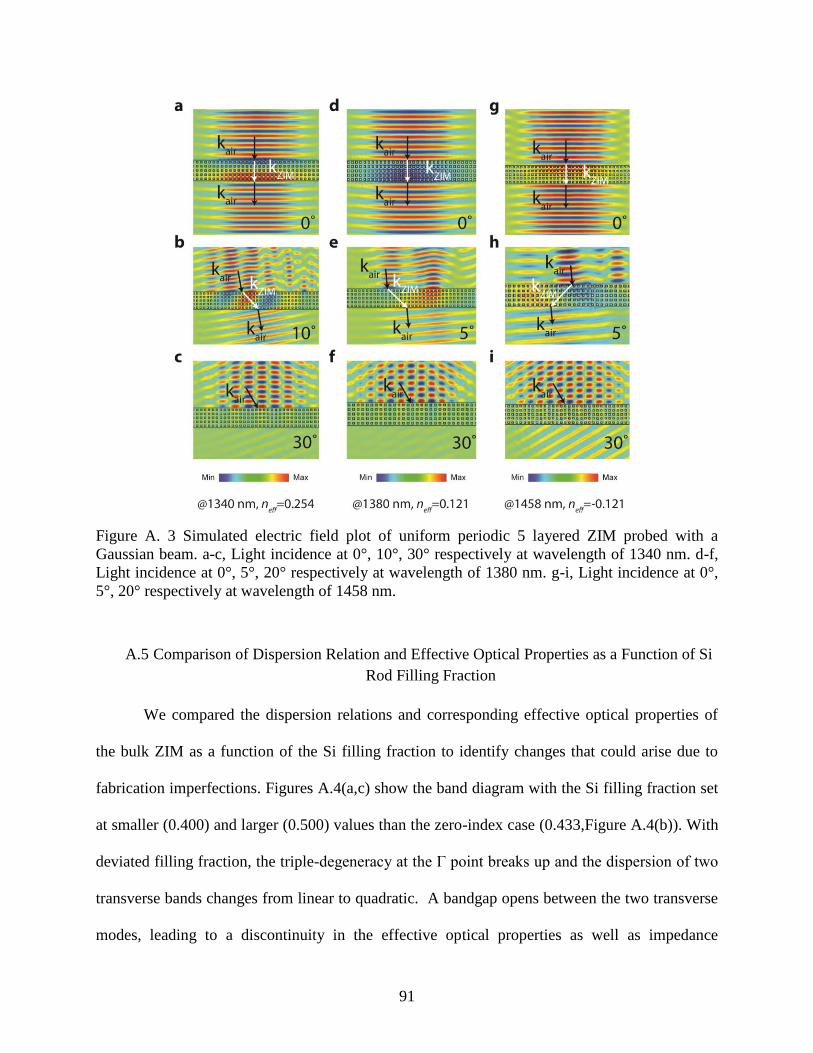
91
Figure A. 3 Simulated electric field plot of uniform periodic 5 layered ZIM probed with a
Gaussian beam. a-c, Light incidence at 0°, 10°, 30° respectively at wavelength of 1340 nm. d-f,
Light incidence at 0°, 5°, 20° respectively at wavelength of 1380 nm. g-i, Light incidence at 0°,
5°, 20° respectively at wavelength of 1458 nm.
A.5 Comparison of Dispersion Relation and Effective Optical Properties as a Function of Si
Rod Filling Fraction
We compared the dispersion relations and corresponding effective optical properties of
the bulk ZIM as a function of the Si filling fraction to identify changes that could arise due to
fabrication imperfections. Figures A.4(a,c) show the band diagram with the Si filling fraction set
at smaller (0.400) and larger (0.500) values than the zero-index case (0.433,Figure A.4(b)). With
deviated filling fraction, the triple-degeneracy at the Γ point breaks up and the dispersion of two
transverse bands changes from linear to quadratic. A bandgap opens between the two transverse
modes, leading to a discontinuity in the effective optical properties as well as impedance
92
mismatch at the band edge, as shown in Figure A.4(d) and Figure A.4(f). A similar effect is
present in the fabricated structure due to non-uniform Si rod size.
Figure A. 4 Band diagram and parameter retrieval for three different filling fractions. a-c, Band
diagram of a square lattice with Si filling fraction of, a 0.400, b 0.433, c 0.500. The lattice
constant is 600 nm, with , . d-f, Corresponding retrieved optical
properties of the bulk material using field averaging. A bandgap appears when the Si filling
fraction deviates from the ideal design. In this case, at the band edge where index is low, the
permittivity and permeability no longer match each other, leading to impedance mismatch to free
space.
A.6 Characterization of Disorder
Here, we provide the lattice positions of the resonators composing the disordered
metamaterials shown in Figures 3.5(a-e) as well as the percentage of disorder. The disorder in
the lattice has been realized by placing the resonators in 2 x 2 and 3 x 3 resonator super cells and
off-setting the resonators’ x and y positions from a nominal spacing of 660 nm.
The percentage disorder in the different lattices is characterized by taking the standard
deviation of the distances between the 4 nearest neighbors to each resonator and normalizing the
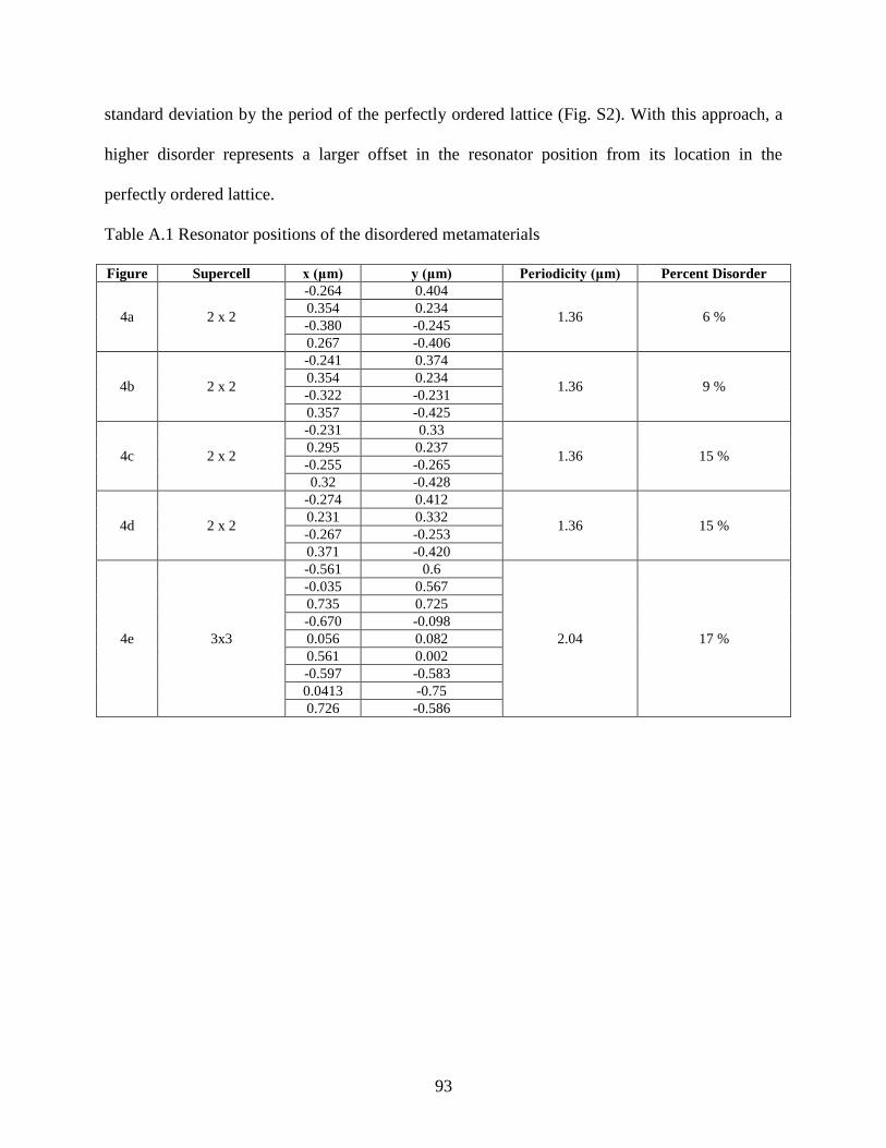
93
standard deviation by the period of the perfectly ordered lattice (Fig. S2). With this approach, a
higher disorder represents a larger offset in the resonator position from its location in the
perfectly ordered lattice.
Table A.1 Resonator positions of the disordered metamaterials
Figure Supercell x (μm) y (μm) Periodicity (μm) Percent Disorder
4a 2 x 2
-0.264 0.404
1.36 6 % 0.354 0.234
-0.380 -0.245
0.267 -0.406
4b 2 x 2
-0.241 0.374
1.36 9 % 0.354 0.234
-0.322 -0.231
0.357 -0.425
4c 2 x 2
-0.231 0.33
1.36 15 % 0.295 0.237
-0.255 -0.265
0.32 -0.428
4d 2 x 2
-0.274 0.412
1.36 15 % 0.231 0.332
-0.267 -0.253
0.371 -0.420
4e 3x3
-0.561 0.6
2.04 17 %
-0.035 0.567
0.735 0.725
-0.670 -0.098
0.056 0.082
0.561 0.002
-0.597 -0.583
0.0413 -0.75
0.726 -0.586
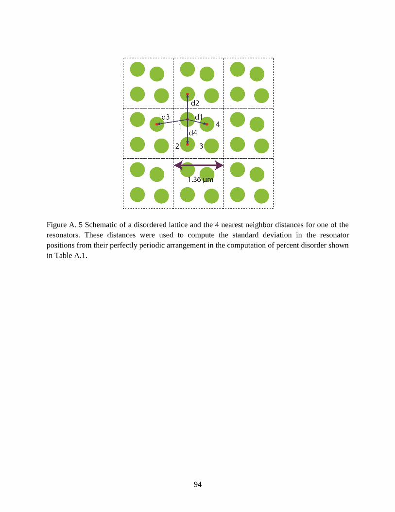
94
Figure A. 5 Schematic of a disordered lattice and the 4 nearest neighbor distances for one of the
resonators. These distances were used to compute the standard deviation in the resonator
positions from their perfectly periodic arrangement in the computation of percent disorder shown
in Table A.1.
95
Bibliography
[1] R. A. Shelby, D. R. Smith, and S. Schultz, “Experimental verification of a negative index
of refraction.,” Science, vol. 292, pp. 77–79, 2001.
[2] S. Zhang, W. Fan, N. C. Panoiu, K. J. Malloy, R. M. Osgood, and S. R. J. Brueck,
“Experimental demonstration of near-infrared negative-index metamaterials.,” Phys. Rev.
Lett., vol. 95, p. 137404, 2005.
[3] V. M. Shalaev, W. Cai, U. K. Chettiar, H.-K. Yuan, A. K. Sarychev, V. P. Drachev, and A.
V Kildishev, “Negative index of refraction in optical metamaterials.,” Opt. Lett., vol. 30,
pp. 3356–3358, 2005.
[4] J. Valentine, S. Zhang, T. Zentgraf, E. Ulin-Avila, D. A. Genov, G. Bartal, and X. Zhang,
“Three-dimensional optical metamaterial with a negative refractive index.,” Nature, vol.
455, no. 7211, pp. 376–9, Sep. 2008.
[5] A. Alù, M. Silveirinha, A. Salandrino, and N. Engheta, “Epsilon-near-zero metamaterials
and electromagnetic sources: Tailoring the radiation phase pattern,” Phys. Rev. B, vol. 75,
no. 15, p. 155410, Apr. 2007.
[6] R. Liu, Q. Cheng, T. Hand, J. J. Mock, T. J. Cui, S. A. Cummer, and D. R. Smith,
“Experimental demonstration of electromagnetic tunneling through an epsilon-near-zero
metamaterial at microwave frequencies.,” Phys. Rev. Lett., vol. 100, p. 023903, 2008.
[7] M. Silveirinha and N. Engheta, “Tunneling of electromagnetic energy through
subwavelength channels and bends using epsilon-near-zero materials.,” Phys. Rev. Lett.,
vol. 97, p. 157403, 2006.
[8] M. Choi, S. H. Lee, Y. Kim, S. B. Kang, J. Shin, M. H. Kwak, K.-Y. Kang, Y.-H. Lee, N.
Park, and B. Min, “A terahertz metamaterial with unnaturally high refractive index.,”
Nature, vol. 470, no. 7334, pp. 369–73, Feb. 2011.
[9] J. B. Pendry, “Negative Refraction Makes a Perfect Lens,” Physical Review Letters, vol.
85. pp. 3966–3969, 2000.
[10] N. Fang, H. Lee, C. Sun, and X. Zhang, “Sub-diffraction-limited optical imaging with a
silver superlens.,” Science, vol. 308, pp. 534–537, 2005.
[11] J. B. Pendry, D. Schurig, and D. R. Smith, “Controlling electromagnetic fields.,” Science,
vol. 312, pp. 1780–1782, 2006.
96
[12] D. Schurig, J. J. Mock, B. J. Justice, S. A. Cummer, J. B. Pendry, A. F. Starr, and D. R.
Smith, “Metamaterial electromagnetic cloak at microwave frequencies.,” Science, vol. 314,
pp. 977–980, 2006.
[13] J. Valentine, J. Li, T. Zentgraf, G. Bartal, and X. Zhang, “An optical cloak made of
dielectrics.,” Nat. Mater., vol. 8, no. 7, pp. 568–71, Jul. 2009.
[14] A. Boltasseva and H. A. Atwater, “Materials science. Low-loss plasmonic metamaterials.,”
Science (80-. )., vol. 331, no. 6015, pp. 290–1, Jan. 2011.
[15] N. I. Zheludev, “Applied physics. The road ahead for metamaterials.,” Science (80-. )., vol.
328, no. 5978, pp. 582–583, Apr. 2010.
[16] C. M. Soukoulis and M. Wegener, “Past achievements and future challenges in the
development of three-dimensional photonic metamaterials,” Nat. Photonics, vol. 5, no. 9,
pp. 523–530, Jul. 2011.
[17] J. Zhou, T. Koschny, M. Kafesaki, E. N. Economou, J. B. Pendry, and C. M. Soukoulis,
“Saturation of the Magnetic Response of Split-Ring Resonators at Optical Frequencies,”
Phys. Rev. Lett., vol. 95, no. 22, p. 223902, Nov. 2005.
[18] D. Smith, W. Padilla, D. Vier, S. Nemat-Nasser, and S. Schultz, “Composite Medium with
Simultaneously Negative Permeability and Permittivity,” Phys. Rev. Lett., vol. 84, no. 18,
pp. 4184–4187, May 2000.
[19] H. C. van de Hulst, Light Scattering by Small Particles. Courier Dover Publications, 2012,
p. 470.
[20] C. M. Soukoulis and M. Wegener, “Past achievements and future challenges in the
development of three-dimensional photonic metamaterials,” Nat. Photonics, vol. 5, no. 9,
pp. 523–530, Jul. 2011.
[21] Y. Liu and X. Zhang, “Metamaterials: a new frontier of science and technology.,” Chem.
Soc. Rev., vol. 40, no. 5, pp. 2494–507, May 2011.
[22] V. G. Veselago, “The electrodynamics of substances with simultaneously negative values
of ε and μ,” Sov. Phys. Uspekhi, vol. 10, pp. 509–514, 1968.
[23] J. Pendry, A. Holden, W. Stewart, and I. Youngs, “Extremely Low Frequency Plasmons in
Metallic Mesostructures,” Phys. Rev. Lett., vol. 76, no. 25, pp. 4773–4776, Jun. 1996.
[24] J. B. Pendry, A. J. Holden, D. J. Robbins, and W. J. Stewart, “Magnetism from conductors
and enhanced nonlinear phenomena,” IEEE Trans. Microw. Theory Tech., vol. 47, 1999.
97
[25] C. García-Meca, R. Ortuño, F. J. Rodríguez-Fortuño, J. Martí, and A. Martínez, “Double-
negative polarization-independent fishnet metamaterial in the visible spectrum,” Opt. Lett.,
vol. 34, no. 10, p. 1603, May 2009.
[26] J. Valentine, S. Zhang, T. Zentgraf, E. Ulin-Avila, D. A. Genov, G. Bartal, and X. Zhang,
“Three-dimensional optical metamaterial with a negative refractive index.,” Nature, vol.
455, pp. 376–379, 2008.
[27] C. García-Meca, J. Hurtado, J. Martí, A. Martínez, W. Dickson, and A. V. Zayats, “Low-
Loss Multilayered Metamaterial Exhibiting a Negative Index of Refraction at Visible
Wavelengths,” Phys. Rev. Lett., vol. 106, no. 6, p. 067402, Feb. 2011.
[28] V. M. Shalaev, “Optical negative-index metamaterials,” Nat. Photonics, vol. 1, no. 1, pp.
41–48, 2007.
[29] L. Peng, L. Ran, H. Chen, H. Zhang, J. A. Kong, and T. M. Grzegorczyk, “Experimental
observation of left-handed behavior in an array of standard dielectric resonators.,” Phys.
Rev. Lett., vol. 98, p. 157403, 2007.
[30] L. Lewin, “The electrical constants of a material loaded with spherical particles,” J. Inst.
Electr. Eng. III Radio Commun. Eng., vol. 94, pp. 65–68, 1947.
[31] S. O’Brien and J. B. Pendry, “Photonic band-gap effects and magnetic activity in
dielectric composites,” Journal of Physics: Condensed Matter, vol. 14. pp. 4035–4044,
2002.
[32] B. Ai, Y. Yu, H. Möhwald, L. Wang, and G. Zhang, “Resonant optical transmission
through topologically continuous films.,” ACS Nano, vol. 8, no. 2, pp. 1566–75, Feb. 2014.
[33] B. Ai, Y. Yu, H. Möhwald, and G. Zhang, “Novel 3D Au nanohole arrays with
outstanding optical properties.,” Nanotechnology, vol. 24, no. 3, p. 035303, Jan. 2013.
[34] S. J. Barcelo, S. Lam, G. A. Gibson, X. Sheng, and D. Henze, “Nanosphere lithography
based technique for fabrication of large area , well ordered metal particle arrays Abstract :
Nanosphere lithography based technique for fabrication of large area , well ordered metal
particle arrays,” 2012.
[35] S. L. Cheng, C. Y. Chen, and S. W. Lee, “Kinetic investigation of the electrochemical
synthesis of vertically-aligned periodic arrays of silicon nanorods on (001)Si substrate,”
Thin Solid Films, vol. 518, no. 6, pp. S190–S195, Jan. 2010.
[36] C. Geng, L. Zheng, J. Yu, Q. Yan, X. Wang, G. Shen, and D. Shen, “Monolayer colloidal
mask with tunable interstice size for nanosphere lithography,” Thin Solid Films, vol. 544,
pp. 83–87, Oct. 2013.
98
[37] K. Kempa, B. Kimball, J. Rybczynski, Z. P. Huang, P. F. Wu, D. Steeves, M. Sennett, M.
Giersig, D. V. G. L. N. Rao, D. L. Carnahan, D. Z. Wang, J. Y. Lao, W. Z. Li, and Z. F.
Ren, “Photonic Crystals Based on Periodic Arrays of Aligned Carbon Nanotubes,” Nano
Lett., vol. 3, no. 1, pp. 13–18, Jan. 2003.
[38] P.-C. Li and E. T. Yu, “Large-area omnidirectional antireflection coating on low-index
materials,” J. Opt. Soc. Am. B, vol. 30, no. 10, p. 2584, Sep. 2013.
[39] P.-C. Li and E. T. Yu, “Flexible, low-loss, large-area, wide-angle, wavelength-selective
plasmonic multilayer metasurface,” J. Appl. Phys., vol. 114, no. 13, p. 133104, Oct. 2013.
[40] X. H. Li, P. C. Li, D. Z. Hu, D. M. Schaadt, and E. T. Yu, “Angular dependence of light
trapping in In0.3Ga0.7As/GaAs quantum-well solar cells,” J. Appl. Phys., vol. 115, no. 4,
p. 044303, Jan. 2014.
[41] J. Rybczynski, U. Ebels, and M. Giersig, “Large-scale, 2D arrays of magnetic
nanoparticles,” Colloids Surfaces A Physicochem. Eng. Asp., vol. 219, no. 1–3, pp. 1–6,
Jun. 2003.
[42] P. I. Stavroulakis, N. Christou, and D. Bagnall, “Improved deposition of large scale
ordered nanosphere monolayers via liquid surface self-assembly,” Mater. Sci. Eng. B, vol.
165, no. 3, pp. 186–189, Dec. 2009.
[43] A. Trzaskowska, S. Mielcarek, B. Graczykowski, B. Mroz, P. Patoka, and M. Giersig,
“The effect of nickel nanostructure on surface waves propagation in silicon support,” J.
Alloys Compd., vol. 527, pp. 96–100, Jun. 2012.
[44] F. Xie, A. Centeno, B. Zou, M. P. Ryan, D. J. Riley, and N. M. Alford, “Tunable synthesis
of ordered zinc oxide nanoflower-like arrays.,” J. Colloid Interface Sci., vol. 395, pp. 85–
90, Apr. 2013.
[45] Y. Yu, B. Ai, H. Möhwald, Z. Zhou, G. Zhang, and B. Yang, “Fabrication of Binary and
Ternary Hybrid Particles Based on Colloidal Lithography,” Chem. Mater., vol. 24, no. 23,
pp. 4549–4555, Dec. 2012.
[46] X. Meng and D. Qiu, “Gas-flow-induced reorientation to centimeter-sized two-
dimensional colloidal single crystal of polystyrene particle.,” Langmuir, vol. 30, no. 11,
pp. 3019–23, Mar. 2014.
[47] C. L. Cheung, R. J. Nikolić, C. E. Reinhardt, and T. F. Wang, “Fabrication of nanopillars
by nanosphere lithography,” Nanotechnology, vol. 17, no. 5, pp. 1339–1343, Mar. 2006.
[48] C.-C. Ho, P.-Y. Chen, K.-H. Lin, W.-T. Juan, and W.-L. Lee, “Fabrication of monolayer
of polymer/nanospheres hybrid at a water-air interface.,” ACS Appl. Mater. Interfaces, vol.
3, no. 2, pp. 204–8, Feb. 2011.
99
[49] L. Li, T. Zhai, H. Zeng, X. Fang, Y. Bando, and D. Golberg, “Polystyrene sphere-assisted
one-dimensional nanostructure arrays: synthesis and applications,” J. Mater. Chem., vol.
21, no. 1, p. 40, 2011.
[50] X. Cai, R. Zhu, and G. Hu, “Experimental study for metamaterials based on dielectric
resonators and wire frame,” Metamaterials, vol. 2, no. 4, pp. 220–226, Dec. 2008.
[51] Q. Zhao, L. Kang, B. Du, H. Zhao, Q. Xie, X. Huang, B. Li, J. Zhou, and L. Li,
“Experimental demonstration of isotropic negative permeability in a three-dimensional
dielectric composite.,” Phys. Rev. Lett., vol. 101, p. 027402, 2008.
[52] F. Zhang, Q. Zhao, L. Kang, J. Zhou, and D. Lippens, “Experimental verification of
isotropic and polarization properties of high permittivity-based metamaterial,” Phys. Rev.
B, vol. 80, no. 19, p. 195119, Nov. 2009.
[53] B.-I. Popa and S. Cummer, “Compact Dielectric Particles as a Building Block for Low-
Loss Magnetic Metamaterials,” Phys. Rev. Lett., vol. 100, no. 20, p. 207401, May 2008.
[54] T. Lepetit, E. Akmansoy, and J.-P. Ganne, “Experimental measurement of negative index
in an all-dielectric metamaterial,” Appl. Phys. Lett., vol. 95, no. 12, p. 121101, Sep. 2009.
[55] C. L. Holloway, E. F. Kuester, J. Baker-Jarvis, and P. Kabos, “A double negative (DNG)
composite medium composed of magnetodielectric spherical particles embedded in a
matrix,” IEEE Trans. Antennas Propag., vol. 51, no. 10, pp. 2596–2603, Oct. 2003.
[56] K. C. Huang, M. L. Povinelli, and J. D. Joannopoulos, “Negative effective permeability in
polaritonic photonic crystals,” Appl. Phys. Lett., vol. 85, no. 4, pp. 543–545, 2004.
[57] M. Wheeler, “Three-dimensional array of dielectric spheres with an isotropic negative
permeability at infrared frequencies,” Phys. Rev. B, vol. 72, no. 19, p. 193103, 2005.
[58] A. Ahmadi and H. Mosallaei, “Physical configuration and performance modeling of all-
dielectric metamaterials,” Phys. Rev. B, vol. 77, no. 4, p. 045104, Jan. 2008.
[59] J. Schuller, R. Zia, T. Taubner, and M. Brongersma, “Dielectric Metamaterials Based on
Electric and Magnetic Resonances of Silicon Carbide Particles,” Phys. Rev. Lett., vol. 99,
no. 10, p. 107401, Sep. 2007.
[60] K. Vynck, D. Felbacq, E. Centeno, A. Căbuz, D. Cassagne, and B. Guizal, “All-Dielectric
Rod-Type Metamaterials at Optical Frequencies,” Phys. Rev. Lett., vol. 102, no. 13, p.
133901, Mar. 2009.
[61] J. C. Ginn, I. Brener, D. W. Peters, J. R. Wendt, J. O. Stevens, P. F. Hines, L. I. Basilio, L.
K. Warne, J. F. Ihlefeld, P. G. Clem, and M. B. Sinclair, “Realizing Optical Magnetism
from Dielectric Metamaterials,” Phys. Rev. Lett., vol. 108, no. 9, p. 097402, Feb. 2012.
100
[62] L. I. Basilio, L. K. Warne, W. L. Langston, W. A. Johnson, and M. B. Sinclair,
“Microwave-Frequency, Negative-Index Metamaterial Designs Based on Degenerate
Dielectric Resonators,” IEEE Antennas Wirel. Propag. Lett., vol. 11, pp. 113–116, 2012.
[63] L. K. Warne, L. I. Basilio, W. L. Langston, W. A. Johnson, and M. B. Sinclair,
“PERTURBATION THEORY IN THE DESIGN OF DEGENERATE RECTANGULAR
DIELECTRIC RESONATORS,” Prog. Electromagn. Res. B, vol. 44, pp. 1–29, 2012.
[64] A. Evlyukhin, C. Reinhardt, and B. Chichkov, “Multipole light scattering by nonspherical
nanoparticles in the discrete dipole approximation,” Physical Review B, vol. 84. 2011.
[65] Y. Yang, W. Wang, P. Moitra, I. I. Kravchenko, D. P. Briggs, and J. Valentine,
“Dielectric meta-reflectarray for broadband linear polarization conversion and optical
vortex generation.,” Nano Lett., vol. 14, no. 3, pp. 1394–9, Mar. 2014.
[66] A. E. Miroshnichenko and Y. S. Kivshar, “Fano Resonances in All-Dielectric Oligomers,”
2012.
[67] I. Staude, A. E. Miroshnichenko, M. Decker, N. T. Fofang, S. Liu, E. Gonzales, J.
Dominguez, T. S. Luk, D. N. Neshev, I. Brener, and Y. Kivshar, “Tailoring Directional
Scattering through Magnetic and Electric Resonances in Subwavelength Silicon
Nanodisks.,” ACS Nano, vol. 7, no. 9, pp. 7824–7832, Aug. 2013.
[68] M. Decker, I. Staude, M. Falkner, J. Dominguez, D. N. Neshev, I. Brener, T. Pertsch, and
Y. S. Kivshar, “High-Efficiency Dielectric Huygens’ Surfaces,” Adv. Opt. Mater., p. n/a–
n/a, Jan. 2015.
[69] A. E. Krasnok, C. R. Simovski, P. A. Belov, and Y. S. Kivshar, “Superdirective dielectric
nanoantennas.,” Nanoscale, vol. 6, no. 13, pp. 7354–61, Jul. 2014.
[70] I. Staude, M. Decker, E. Rusak, D. N. Neshev, and I. Brener, “Active Tuning of All-
Dielectric,” no. 4, pp. 4308–4315, 2015.
[71] S. Liu, M. B. Sinclair, T. S. Mahony, Y. C. Jun, S. Campione, J. Ginn, D. A. Bender, J. R.
Wendt, J. F. Ihlefeld, P. G. Clem, J. B. Wright, and I. Brener, “Optical magnetic mirrors
without metals,” Optica, vol. 1, no. 4, p. 250, Oct. 2014.
[72] F. Aieta, M. A. Kats, P. Genevet, and F. Capasso, “Achromatic metasurface optical
components by dispersive phase compensation,” Nov. 2014.
[73] R. M. Bakker, D. Permyakov, Y. F. Yu, D. Markovich, R. Paniagua-Domínguez, L.
Gonzaga, A. Samusev, Y. Kivshar, B. Luk’yanchuk, and A. I. Kuznetsov, “Magnetic and
Electric Hotspots with Silicon Nanodimers.,” Nano Lett., Feb. 2015.
[74] D.-H. Kwon and D. H. Werner, “Low-index metamaterial designs in the visible spectrum,”
Opt. Express, vol. 15, no. 15, p. 9267, Jul. 2007.

101
[75] E. J. R. Vesseur, T. Coenen, H. Caglayan, N. Engheta, and A. Polman, “Experimental
Verification of n=0 Structures for Visible Light,” Phys. Rev. Lett., vol. 110, p. 013902,
2013.
[76] S. Enoch, G. Tayeb, P. Sabouroux, N. Guérin, and P. Vincent, “A metamaterial for
directive emission.,” Phys. Rev. Lett., vol. 89, p. 213902, 2002.
[77] D. Adams, S. Inampudi, T. Ribaudo, D. Slocum, S. Vangala, N. Kuhta, W. Goodhue, V.
Podolskiy, and D. Wasserman, “Funneling Light through a Subwavelength Aperture with
Epsilon-Near-Zero Materials,” Phys. Rev. Lett., vol. 107, no. 13, p. 133901, Sep. 2011.
[78] X. Huang, Y. Lai, Z. H. Hang, H. Zheng, and C. T. Chan, “Dirac cones induced by
accidental degeneracy in photonic crystals and zero-refractive-index materials.,” Nature
materials, vol. 10. pp. 582–586, 2011.
[79] S. Yun, Z. H. Jiang, Q. Xu, Z. Liu, D. H. Werner, and T. S. Mayer, “Low-loss impedance-
matched optical metamaterials with zero-phase delay.,” ACS Nano, vol. 6, pp. 4475–82,
2012.
[80] L.-G. Wang, Z.-G. Wang, J.-X. Zhang, and S.-Y. Zhu, “Realization of Dirac point with
double cones in optics,” Opt. Lett., vol. 34, no. 10, p. 1510, May 2009.
[81] P. Moitra, Y. Yang, Z. Anderson, I. I. Kravchenko, D. P. Briggs, and J. Valentine,
“Realization of an all-dielectric zero-index optical metamaterial,” Nat. Photonics, vol. 7,
no. 10, pp. 791–795, Aug. 2013.
[82] K. S. Novoselov, A. K. Geim, S. V Morozov, D. Jiang, M. I. Katsnelson, I. V Grigorieva,
S. V Dubonos, and A. A. Firsov, “Two-dimensional gas of massless Dirac fermions in
graphene.,” Nature, vol. 438, pp. 197–200, 2005.
[83] I. Tsukerman, “Effective parameters of metamaterials: a rigorous homogenization theory
via Whitney interpolation,” Journal of the Optical Society of America B, vol. 28. p. 577,
2011.
[84] Y. Wu, J. Li, Z.-Q. Zhang, and C. Chan, “Effective medium theory for magnetodielectric
composites: Beyond the long-wavelength limit,” Physical Review B, vol. 74. 2006.
[85] R. W. Ziolkowski, “Propagation in and scattering from a matched metamaterial having a
zero index of refraction.,” Phys. Rev. E. Stat. Nonlin. Soft Matter Phys., vol. 70, p. 046608,
2004.
[86] B. Slovick, Z. G. Yu, M. Berding, and S. Krishnamurthy, “Perfect dielectric-metamaterial
reflector,” Phys. Rev. B, vol. 88, no. 16, p. 165116, Oct. 2013.
102
[87] L. I. Basilio, L. K. Warne, W. L. Langston, W. A. Johnson, and M. B. Sinclair,
“Microwave-Frequency, Negative-Index Metamaterial Designs Based on Degenerate
Dielectric Resonators,” IEEE Antennas Wirel. Propag. Lett., vol. 11, pp. 113–116, 2012.
[88] L. K. Warne, L. I. Basilio, W. L. Langston, W. A. Johnson, and M. B. Sinclair,
“PERTURBATION THEORY IN THE DESIGN OF DEGENERATE RECTANGULAR
DIELECTRIC RESONATORS,” Prog. Electromagn. Res. B, vol. 44, pp. 1–29, 2012.
[89] X. Chen, T. Grzegorczyk, B.-I. Wu, J. Pacheco, and J. Kong, “Robust method to retrieve
the constitutive effective parameters of metamaterials,” Phys. Rev. E, vol. 70, no. 1, p.
016608, Jul. 2004.
[90] D. R. Smith, D. C. Vier, T. Koschny, and C. M. Soukoulis, “Electromagnetic parameter
retrieval from inhomogeneous metamaterials,” Phys. Rev. E, vol. 71, no. 3, p. 036617,
Mar. 2005.
[91] Z. Szabo, G.-H. Park, R. Hedge, and E.-P. Li, “A Unique Extraction of Metamaterial
Parameters Based on Kramers–Kronig Relationship,” IEEE Trans. Microw. Theory Tech.,
vol. 58, no. 10, pp. 2646–2653, Oct. 2010.
[92] C. L. Haynes, A. D. McFarland, M. T. Smith, J. C. Hulteen, and R. P. Van Duyne,
“Angle-Resolved Nanosphere Lithography: Manipulation of Nanoparticle Size, Shape,
and Interparticle Spacing,” J. Phys. Chem. B, vol. 106, no. 8, pp. 1898–1902, Jan. 2002.
[93] V. Karagodsky, F. G. Sedgwick, and C. J. Chang-Hasnain, “Theoretical analysis of
subwavelength high contrast grating reflectors.,” Opt. Express, vol. 18, no. 16, pp. 16973–
88, Aug. 2010.
[94] C. Chase, Y. Rao, W. Hofmann, and C. J. Chang-Hasnain, “1550 nm high contrast grating
VCSEL.,” Opt. Express, vol. 18, no. 15, pp. 15461–6, Jul. 2010.
[95] P. Moitra, B. A. Slovick, Z. Gang Yu, S. Krishnamurthy, and J. Valentine, “Experimental
demonstration of a broadband all-dielectric metamaterial perfect reflector,” Appl. Phys.
Lett., vol. 104, no. 17, p. 171102, Apr. 2014.
[96] “IEEE Xplore Full-Text HTML : Experimental demonstration of an optical artificial
perfect magnetic mirror using dielectric resonators.” [Online]. Available:
http://ieeexplore.ieee.org/xpls/icp.jsp?arnumber=6349206. [Accessed: 10-Feb-2015].
[97] M. Esfandyarpour, E. C. Garnett, Y. Cui, M. D. McGehee, and M. L. Brongersma,
“Metamaterial mirrors in optoelectronic devices.,” Nat. Nanotechnol., vol. 9, no. 7, pp.
542–7, Jul. 2014.
[98] H. W. Deckman, “Natural lithography,” Appl. Phys. Lett., vol. 41, no. 4, p. 377, Aug.
1982.
103
[99] U. C. Fischer, “Submicroscopic pattern replication with visible light,” J. Vac. Sci.
Technol., vol. 19, no. 4, p. 881, Nov. 1981.
[100] A. Nemiroski, M. Gonidec, J. M. Fox, P. Jean-Remy, E. Turnage, and G. M. Whitesides,
“Engineering shadows to fabricate optical metasurfaces.,” ACS Nano, vol. 8, no. 11, pp.
11061–70, Nov. 2014.
[101] J. M. Hoffmann, H. Janssen, D. N. Chigrin, and T. Taubner, “Enhanced infrared
spectroscopy using small-gap antennas prepared with two-step evaporation nanosphere
lithography.,” Opt. Express, vol. 22, no. 12, pp. 14425–32, Jun. 2014.
[102] P. Colson, C. Henrist, and R. Cloots, “Nanosphere Lithography: A Powerful Method for
the Controlled Manufacturing of Nanomaterials,” J. Nanomater., vol. 2013, pp. 1–19, Jan.
2013.
[103] J. C. Hulteen, “Nanosphere lithography: A materials general fabrication process for
periodic particle array surfaces,” J. Vac. Sci. Technol. A Vacuum, Surfaces, Film., vol. 13,
no. 3, p. 1553, May 1995.
[104] E. C. Brown, S. K. Wilke, D. A. Boyd, D. G. Goodwin, and S. M. Haile, “Polymer sphere
lithography for solid oxide fuel cells: a route to functional, well-defined electrode
structures,” J. Mater. Chem., vol. 20, no. 11, p. 2190, Mar. 2010.
[105] J. Chen, P. Dong, D. Di, C. Wang, H. Wang, J. Wang, and X. Wu, “Controllable
fabrication of 2D colloidal-crystal films with polystyrene nanospheres of various
diameters by spin-coating,” Appl. Surf. Sci., vol. 270, pp. 6–15, Apr. 2013.
[106] P. Colson, R. Cloots, and C. Henrist, “Experimental design applied to spin coating of 2D
colloidal crystal masks: a relevant method?,” Langmuir, vol. 27, no. 21, pp. 12800–6, Nov.
2011.
[107] N. Denkov, O. Velev, P. Kralchevski, I. Ivanov, H. Yoshimura, and K. Nagayama,
“Mechanism of formation of two-dimensional crystals from latex particles on substrates,”
Langmuir, vol. 8, no. 12, pp. 3183–3190, Dec. 1992.
[108] P. Jiang and M. J. McFarland, “Large-scale fabrication of wafer-size colloidal crystals,
macroporous polymers and nanocomposites by spin-coating.,” J. Am. Chem. Soc., vol. 126,
no. 42, pp. 13778–86, Oct. 2004.
[109] C.-W. Kuo, J.-Y. Shiu, and P. Chen, “Size- and Shape-Controlled Fabrication of Large-
Area Periodic Nanopillar Arrays,” Chem. Mater., vol. 15, no. 15, pp. 2917–2920, Jul.
2003.
[110] T. J. Rehg and G. Higgins, “Spin coating of colloidal suspensions,” AIChE J., vol. 38, no.
4, pp. 489–501, Apr. 1992.

104
[111] Y. . Zheng, S. . Chua, C. H. . Huan, and Z. . Miao, “Selective growth of GaAs quantum
dots on the triangle nanocavities bounded by SiO2 mask on Si substrate by MBE,” J.
Cryst. Growth, vol. 268, no. 3–4, pp. 369–374, Aug. 2004.
[112] S. Okazaki, “Resolution limits of optical lithography,” J. Vac. Sci. Technol. B
Microelectron. Nanom. Struct., vol. 9, no. 6, p. 2829, Nov. 1991.
[113] Y. Xia and G. M. Whitesides, “Soft Lithography,” Angew. Chemie Int. Ed., vol. 37, no. 5,
pp. 550–575, Mar. 1998.
[114] A. S. Hall, S. A. Friesen, and T. E. Mallouk, “Wafer-scale fabrication of plasmonic
crystals from patterned silicon templates prepared by nanosphere lithography.,” Nano Lett.,
vol. 13, no. 6, pp. 2623–7, Jun. 2013.
[115] J.-T. Zhang, L. Wang, X. Chao, S. S. Velankar, and S. a. Asher, “Vertical spreading of
two-dimensional crystalline colloidal arrays,” J. Mater. Chem. C, vol. 1, no. 38, p. 6099,
2013.
[116] A. B. Dark, P. Mode, M. Nanodisk, A. Fabricated, and N.-L. Lithography, “Observation
of Absorption-Dominated Bonding Dark Plasmon Mode from Metal À Insulator À Metal
Nanodisk Arrays Fabricated by Nanospherical-,” no. 4, pp. 3390–3396, 2012.
[117] Y.-C. Chang, H.-C. Chung, S.-C. Lu, and T.-F. Guo, “A large-scale sub-100 nm Au
nanodisk array fabricated using nanospherical-lens lithography: a low-cost localized
surface plasmon resonance sensor.,” Nanotechnology, vol. 24, no. 9, p. 095302, Mar. 2013.
[118] Y.-C. Chang, S.-C. Lu, H.-C. Chung, S.-M. Wang, T.-D. Tsai, and T.-F. Guo, “High-
Throughput Nanofabrication of Infra-red and Chiral Metamaterials using Nanospherical-
Lens Lithography,” Sci. Rep., vol. 3, Nov. 2013.
[119] W. Wu, A. Katsnelson, O. G. Memis, and H. Mohseni, “A deep sub-wavelength process
for the formation of highly uniform arrays of nanoholes and nanopillars,” Nanotechnology,
vol. 18, no. 48, p. 485302, Dec. 2007.
[120] C.-H. Hou, S.-Z. Tseng, C.-H. Chan, T.-J. Chen, H.-T. Chien, F.-L. Hsiao, H.-K. Chiu, C.-
C. Lee, Y.-L. Tsai, and C.-C. Chen, “Output power enhancement of light-emitting diodes
via two-dimensional hole arrays generated by a monolayer of microspheres,” Appl. Phys.
Lett., vol. 95, no. 13, p. 133105, 2009.
[121] F. Aieta, P. Genevet, M. A. Kats, N. Yu, R. Blanchard, Z. Gaburro, and F. Capasso,
“Aberration-free ultrathin flat lenses and axicons at telecom wavelengths based on
plasmonic metasurfaces.,” Nano Lett., vol. 12, no. 9, pp. 4932–6, Sep. 2012.
[122] C. Pfeiffer and A. Grbic, “Metamaterial huygens’ surfaces: Tailoring wave fronts with
reflectionless sheets,” Phys. Rev. Lett., vol. 110, p. 197401, 2013.
105
[123] N. Yu, P. Genevet, M. A. Kats, F. Aieta, J.-P. Tetienne, F. Capasso, and Z. Gaburro,
“Light Propagation with Phase Discontinuities: Generalized Laws of Reflection and
Refraction,” Science, vol. 334. pp. 333–337, 2011.
[124] L. Huang, X. Chen, H. Mühlenbernd, G. Li, B. Bai, Q. Tan, G. Jin, T. Zentgraf, and S.
Zhang, “Dispersionless phase discontinuities for controlling light propagation.,” Nano
Lett., vol. 12, no. 11, pp. 5750–5, Nov. 2012.
[125] N. Yu and F. Capasso, “Flat optics with designer metasurfaces.,” Nat. Mater., vol. 13, no.
2, pp. 139–50, Feb. 2014.
[126] P. Genevet and F. Capasso, “Holographic optical metasurfaces: a review of current
progress.,” Rep. Prog. Phys., vol. 78, no. 2, p. 024401, Jan. 2015.
[127] G. Zheng, H. Mühlenbernd, M. Kenney, G. Li, T. Zentgraf, and S. Zhang, “Metasurface
holograms reaching 80% efficiency,” Nat. Nanotechnol., no. February, pp. 1–6, Feb. 2015.
[128] S. Pancharatnam, “Generalized theory of interference, and its applications,” Proc. Indian
Acad. Sci. - Sect. A, vol. 44, no. 5, pp. 247–262.
[129] M. V. Berry, “The Adiabatic Phase and Pancharatnam's Phase for Polarized Light,” J.
Mod. Opt, vol 34, no. 11, pp. 1401–1407, 1987.
[130] L. Marrucci, C. Manzo, and D. Paparo, “Pancharatnam-Berry phase optical elements for
wave front shaping in the visible domain: Switchable helical mode generation,” Appl.
Phys. Lett., vol. 88, no. 22, p. 221102, 2006.
[131] M. Kang, J. Chen, X.-L. Wang, and H.-T. Wang, “Twisted vector field from an
inhomogeneous and anisotropic metamaterial,” J. Opt. Soc. Am. B, vol. 29, no. 4, p. 572,
Mar. 2012.
[132] M. Kang, T. Feng, H.-T. Wang, and J. Li, “Wave front engineering from an array of thin
aperture antennas.,” Opt. Express, vol. 20, no. 14, pp. 15882–90, Jul. 2012.
[133] F. Gori, “Measuring Stokes parameters by means of a polarization grating,” Opt. Lett., vol.
24, no. 9, p. 584, May 1999.
[134] Z. Bomzon, G. Biener, V. Kleiner, and E. Hasman, “Space-variant Pancharatnam-Berry
phase optical elements with computer-generated subwavelength gratings,” Opt. Lett., vol.
27, no. 13, p. 1141, Jul. 2002.
[135] D. Lin, P. Fan, E. Hasman, and M. L. Brongersma, “Dielectric gradient metasurface
optical elements,” vol. 345, no. 6194, pp. 5189–5192, 2014.

106
[136] D. Slocum, D. C. Adams, S. Inampudi, S. Vangala, W. D. Goodhue, V. A. Podolskiy, and
D. Wasserman, “Funneling light through a subwavelength aperture using epsilon-near-
zero materials,” CLEO 2011 - Laser Sci. to Photonic Appl., pp. 1–2, 2011.
[137] A. Miroshnichenko and Y. Kivshar, “Engineering Fano resonances in discrete arrays,”
Phys. Rev. E, vol. 72, no. 5, p. 056611, Nov. 2005.
[138] S. Zhang, D. A. Genov, Y. Wang, M. Liu, and X. Zhang, “Plasmon-Induced Transparency
in Metamaterials,” Phys. Rev. Lett., vol. 101, no. 4, p. 047401, Jul. 2008.
[139] J. Gu, R. Singh, X. Liu, X. Zhang, Y. Ma, S. Zhang, S. A. Maier, Z. Tian, A. K. Azad, H.-
T. Chen, A. J. Taylor, J. Han, and W. Zhang, “Active control of electromagnetically
induced transparency analogue in terahertz metamaterials.,” Nat. Commun., vol. 3, p. 1151,
Jan. 2012.
[140] N. Liu, T. Weiss, M. Mesch, L. Langguth, U. Eigenthaler, M. Hirscher, C. Sönnichsen,
and H. Giessen, “Planar metamaterial analogue of electromagnetically induced
transparency for plasmonic sensing.,” Nano Lett., vol. 10, no. 4, pp. 1103–7, Apr. 2010.
[141] N. Papasimakis, V. A. Fedotov, N. I. Zheludev, and S. L. Prosvirnin, “Metamaterial
Analog of Electromagnetically Induced Transparency,” Phys. Rev. Lett., vol. 101, no. 25,
p. 253903, Dec. 2008.
[142] S. Xiao, V. P. Drachev, A. V Kildishev, X. Ni, U. K. Chettiar, H.-K. Yuan, and V. M.
Shalaev, “Loss-free and active optical negative-index metamaterials.,” Nature, vol. 466,
no. 7307, pp. 735–8, Aug. 2010.
[143] P. Tassin, L. Zhang, T. Koschny, E. N. Economou, and C. M. Soukoulis, “Low-Loss
Metamaterials Based on Classical Electromagnetically Induced Transparency,” Phys. Rev.
Lett., vol. 102, no. 5, p. 053901, Feb. 2009.
[144] N. Liu, L. Langguth, T. Weiss, J. Kästel, M. Fleischhauer, T. Pfau, and H. Giessen,
“Plasmonic analogue of electromagnetically induced transparency at the Drude damping
limit.,” Nat. Mater., vol. 8, no. 9, pp. 758–62, Sep. 2009.
[145] S. Zhang, Y.-S. Park, J. Li, X. Lu, W. Zhang, and X. Zhang, “Negative refractive index in
chiral metamaterials.,” Phys. Rev. Lett., vol. 102, p. 023901, 2009.
[146] Y. Tang and A. E. Cohen, “Optical Chirality and Its Interaction with Matter,” Phys. Rev.
Lett., vol. 104, no. 16, p. 163901, Apr. 2010.
[147] M. Decker, M. W. Klein, M. Wegener, and S. Linden, “Circular dichroism of planar chiral
magnetic metamaterials.,” Opt. Lett., vol. 32, pp. 856–858, 2007.
[148] E. Plum, V. A. Fedotov, and N. I. Zheludev, “Optical activity in extrinsically chiral
metamaterial,” Appl. Phys. Lett., vol. 93, no. 19, p. 191911, Nov. 2008.
107
[149] N. N. Rosanov, N. V. Vysotina, A. N. Shatsev, A. S. Desyatnikov, and Y. S. Kivshar,
“Knotted Solitons in Nonlinear Magnetic Metamaterials,” Phys. Rev. Lett., vol. 108, no.
13, p. 133902, Mar. 2012.
[150] N. N. Rosanov, N. V Vysotina, A. N. Shatsev, I. V Shadrivov, D. A. Powell, and Y. S.
Kivshar, “Discrete dissipative localized modes in nonlinear magnetic metamaterials.,” Opt.
Express, vol. 19, no. 27, pp. 26500–6, Dec. 2011.
[151] Y. S. Kivshar, “Tunable and nonlinear metamaterials: toward functional metadevices,”
Adv. Nat. Sci. Nanosci. Nanotechnol., vol. 5, no. 1, p. 013001, Nov. 2013.
[152] K. O’Brien, H. Suchowski, J. Rho, A. Salandrino, B. Kante, X. Yin, and X. Zhang,
“Predicting nonlinear properties of metamaterials from the linear response,” Nat. Mater.,
vol. 14, no. 4, pp. 379–383, Feb. 2015.
[153] “Nonlinear, Tunable and Active Metamaterials | Springer.” [Online]. Available:
http://www.springer.com/us/book/9783319083858. [Accessed: 04-May-2015].
[154] L. Kang, Y. Cui, S. Lan, S. P. Rodrigues, M. L. Brongersma, and W. Cai, “Electrifying
photonic metamaterials for tunable nonlinear optics.,” Nat. Commun., vol. 5, p. 4680, Jan.
2014.
[155] M. Hentschel, T. Utikal, H. Giessen, and M. Lippitz, “Quantitative modeling of the third
harmonic emission spectrum of plasmonic nanoantennas.,” Nano Lett., vol. 12, no. 7, pp.
3778–82, Jul. 2012.
[156] L. Huang, X. Chen, H. Mühlenbernd, H. Zhang, S. Chen, B. Bai, Q. Tan, G. Jin, K.-W.
Cheah, C.-W. Qiu, J. Li, T. Zentgraf, and S. Zhang, “Three-dimensional optical
holography using a plasmonic metasurface,” Nat. Commun., vol. 4, Nov. 2013.
[157] S. Pleasants, “Metamaterials: Perfect reflection,” Nat. Photonics, vol. 8, no. 7, pp. 498–
498, Jun. 2014.
[158] F. G. Della Corte, M. Esposito Montefusco, L. Moretti, I. Rendina, and G. Cocorullo,
“Temperature dependence analysis of the thermo-optic effect in silicon by single and
double oscillator models,” J. Appl. Phys., vol. 88, no. 12, p. 7115, Dec. 2000.
[159] R. Soref and B. Bennett, “Electrooptical effects in silicon,” IEEE J. Quantum Electron.,
vol. 23, no. 1, pp. 123–129, Jan. 1987.
[160] F. Gan, T. Barwicz, M. A. Popovic, M. S. Dahlem, C. W. Holzwarth, P. T. Rakich, H. I.
Smith, E. P. Ippen, and F. X. Kartner, “Maximizing the Thermo-Optic Tuning Range of
Silicon Photonic Structures,” in 2007 Photonics in Switching, 2007, pp. 67–68.

108
[161] D. Kwong, A. Hosseini, J. Covey, Y. Zhang, X. Xu, H. Subbaraman, and R. T. Chen,
“On-chip silicon optical phased array for two-dimensional beam steering.,” Opt. Lett., vol.
39, no. 4, pp. 941–4, Feb. 2014.
[162] J. Sun, E. Timurdogan, A. Yaacobi, E. S. Hosseini, and M. R. Watts, “Large-scale
nanophotonic phased array.,” Nature, vol. 493, no. 7431, pp. 195–9, Jan. 2013.
[163] Q. Xu, B. Schmidt, S. Pradhan, and M. Lipson, “Micrometre-scale silicon electro-optic
modulator.,” Nature, vol. 435, no. 7040, pp. 325–7, May 2005.