microwave transmission lines - department of electrical engineering
TRANSCRIPT

Microwave Transmission Lines
An Introduction to the Basics
Debapratim Ghosh
Department of Electrical Engineering
Indian Institute of Technology Bombay

Abstract
This document presents an introduction to the basics of microwave transmission lines. It is important to
understand the principles underlying the propagation and transmission of high-frequency signals, which
are vital in areas such as communications circuit design as well as in high-frequency processor cores, and it
is a well known fact that contemporary processors are clocked by frequencies as high as 3GHz! Designs at
such high frequencies require careful consideration so as to minimize losses and to ensure maximum power
transmission. This document starts by giving an insight into the basics of transmission lines and wave
propagation theory. This is then followed by different transmission line technologies adopted in modern
electronic systems for fabrication.

Chapter 1
Introduction
Microwaves are a part of the electromagnetic spectrum. Usually, waves with wavelengths ranging from
as low as a few millimeters to almost a metre are classified as microwaves. Conventional definition for the
microwave frequency range is from 300MHz − 300GHz. A very important question is the reason behind
studying microwaves. What do these have to offer, and how are they advantageous? The answer is that
most of modern electronic communication engineering make use of microwaves. Then again, what do mi-
crowaves have that makes them suitable for use in comminication engineering? Let us consider for example,
a mobile phone, an indispensable communication tool for all. Supposing that a mobile uses the GSM1800
band, i.e. it makes use of communication frequencies of about 1800MHz. For proper wireless transmission
and reception, every device requires a transmission/reception antenna, tuned to the frequency of operation,
and the antenna size is usually determined by the wavelength λ. A good antenna size approximation is
λ/4, and for an 1800MHz wave, the antenna size required would be around 4.2cm. What would be the
required antenna size if the transmission frequency would be low, say for example 100Hz?
This leads to another interesting question. If antenna sizes can be reduced considerably by using
high frequenices, why not use much higher frequencies? Above microwaves, there are the infra-red and
visible light spectra, and even above, there are ultraviolet rays, X-rays and gamma rays. Many of the
high-frequency waves such as the UV rays and above, are detrimental for health as they are ionizing radi-
ations. This also means that for satellite communications, these waves would be afftected by the earth’s
atmosphere. Moreover, even non-ionizing waves such as infrared rays are easily affected by atmospheric
constituents and do not have obstruction penetration strength. Would these make good candidates for
wireless communication, especially mobile phones, where users are often inside their houses, surrounded
by thick walls?
1

1.1 The High Frequency Circuit Analysis Problem
In this section, we will see the method of analysis for low-frequency circuits and from thereon, examine
why this cannot be used at high frequencies.
Consider a circuit with a source Vs(t) and load RL, as in Figure 1.1. The connection between them is by
means of two conductors (whose resistance is assumed to be low). An initial look at this circuit shows that
at any instant of time t, the voltage across the load Vo(t) will equal the source voltage i.e., Vo(t) = Vs(t).
In such cases, the wire length l has absolutely no role is determining Vo(t) (assuming l is small enough).
l
Vs (t) RL Vo (t)
Figure 1.1: Simple source-load circuit
This approximation however, is true for low frequencies only. Consider the source sine wave traveling
along the length l with a wave velocity v. Define the propagation time from source to load tp as
tp =v
l
Define a voltage along the line, which is a function of both time t and the position on the line x, where
0 ≤ x ≤ l. Assume x = 0 denotes the source end and x = l the load end. Consider the source voltage Vs(t)
waveform shown in Figure 1.2. Consider the source voltage at t = 0 i.e. Vs(t = t0, x = 0) = V1. Then,
the load voltage will equal V1 only when t = t0 + tp, i.e. after the line propagation delay time. But, then,
Vs(t = t0 +tp, x = 0) = V2. Voltages V1 and V2 are likely to e largely different, if the wave frequency is high,
i.e. the time period T is small. Clearly, it is seen that the voltage varies along the length of the line when
the frequency is high, or in general, when the wave dimensions become comparable to the dimensions of
the circuit components. Hence, the lumped circuit theorems at low frequencies cannot directly be applied
to analyzing circuits at high frequencies. The voltage at any given point on the line is now a function of
time as well as space (or position).
The starting method of analyzing high frequency transmission lines is to consider a small section of the
line, where the voltage is assumed not to change significantly over the length of the section, wherein the
laws of lumped circuit theory can be applied.
2

t
Vs (t)
T
1
2
tp
to
V
V
Figure 1.2: Sinusoidal source voltage
1.2 Voltage and Current along a Transmission Line
Let us now study the transmission line behaviour to an input, in greater detail. Consider a sinusoidal
signal traveling along the line. Irrespective of the kind of signal traveling through the line, the conductors
will have some resistance. Let R denote the resistance of the line per unit length. Also, this two-conductor
connection is separated by a dielectric, which may have a parasitic conductance component, denoted per
unit length as G. Due to the traveling sine wave, a time-varying magnetic field will be generated around
each conductor, while a mutual electric field will interact between the two conductors. The magnetic
field leads to a distributed inductance along the line, while the interacting electric field leads to a mutual
capacitance. Denote the per unit length inductance and capacitance as L and C respectively. Consider an
infinitesimally small section of the transmission line ∆x, where the voltage variation over the length ∆x is
negligible. The section of such a size can then be expressed as an R−L−G−C lumped circuit as shown
in Figure 1.3.
Since we have assumed R,L,G,C to be the per unit length line parameters, the actual resistance,
capacitance etc. for this section of the transmission line will be the product of these parameters and the
length in consideration, i.e., ∆x, which is assumed to be infinitesimally small. Note that we deal with
the positional voltages and currents in this circuit as a consequence of the discussion in Section 1.1. The
voltage and current at the left end of the line are denoted as V (x) and I(x), while at a distance of ∆x
towards the right are V (x + ∆x) and I(x + ∆x).
Assume that the frequency of operation is f , and the angular frequency Ω = 2πf . Now, applying
Kirchhoff’s Voltage Law (KVL) in the loop, we have
V (x + ∆x) = V (x) − I(x)(R + jΩL)∆x
3

R∆x L∆x
G∆x C∆xV(x) V(x+∆x)I(x) I(x+∆x)
Figure 1.3: Small section of a transmission line- lumped circuit equivalent
∴
V (x + ∆x) − V (x)
∆x= −I(x)(R + jΩL)
taking the limiting case of ∆x → 0
lim∆x→0
V (x + ∆x) − V (x)
∆x=
dV
dx= −(R + jΩL)I (1.1)
Similarly, by applying Kirchhoff’s Current Law (KCL) at the right node, we get
dI
dx= −(G + jΩC)V (1.2)
We now have two differeintial equations in two variables, V and I. To make them easier to solve,
differentiate both (1.1) and (1.2) by x again. We now have two equations
d2V
dx2= (R + jΩL)(G + jΩC)V (1.3)
d2I
dx2= (R + jΩL)(G + jΩC)I (1.4)
Let γ2 = (R+jΩL)(G+jΩC). The significance of the term γ will be dicussed later. The two differential
equations now becomed2V
dx2= γ2V (1.5)
d2I
dx2= γ2I (1.6)
Equations (1.5) and (1.6) are called the wave equations. Let us see why. These equations are now
simplified, which are ordinary second order differential equations, which can be solved independently.
Consider the voltage equation (1.5). Its solution is of the form
V (x) = V1e−γx + V2e
γx (1.7)
4

The solution for V (x) is a function of the position on the transmission line alone. However, the complete
solution for V (x) is a function of both x and time t. Consider a sinusoidal input to the transmission line,
which can be represented by a complex exponential ejΩt. Thus, the complete voltage solution on the line
is
V (x, t) = V1e−γxejΩt + V2e
γxejΩt (1.8)
Recall that γ2 = (R + jΩL)(G + jΩC). Thus γ in general, is a complex quantity. Therefore, let
γ = α + jβ. V (x, t) can now be represented as
V (x, t) = V1e−αxej(Ωt−βx) + V2e
αxej(Ωt+βx) (1.9)
This gives an interesting result. Consider, for simplicity, α = 0. Let us focus on the first term of (1.9),
i.e. V1ej(Ωt−βx). This quantity is complex, comprising of a sine and a cosine component. Consider the real
part of this term, i.e. V1 cos(Ωt − βx). If this term is now evaluated for various values of x in increasing
order, the results are as shown in Figure 1.4.
x = xo
x = x1 > xo
x = x2 > x1
A
A
A
Figure 1.4: Wave propagation as a function of x
Observe the point A on the wave. As the value of x increases, the point A shifts to the right, indicating
the wave “propagation” in the positive x direction. Similarly, the term V2 cos(Ωt + βx), which is the real
part of the second term of the solution for V (x, t), indicates a wave traveling in the negative x direction
(work it out yourself, for different values of x). This indicates that when a transmission line is excited with
an AC input, there are two waves traveling- from source to load and vice-versa. Likewise, the current will
also propagate in two directions!
5

Chapter 2
Transmission Line Characteristics
In the previous chapter, we had an initial look at the lumped-component sectional representation of
a transmission line, and that waves propagate in two directions, once the line is excited with a voltage
input. In this chapter, we will study the transmission line characteristics in greater detail, such as the line
behaviour with different kinds of load, issues of losses and different techniques for analysis, and applications
of transmission lines.
2.1 Wave Propagation in Transmission Lines
We have seen that in general, the complete solution for the voltage and current along a transmission
line is given as
V (x, t) = V1e−αxej(Ωt−βx) + V2e
αxej(Ωt+βx)
I(x, t) = I1e−αxej(Ωt−βx) + I2e
αxej(Ωt+βx)(2.1)
Note that γ = α + jβ. Let us investigate the quantity γ in more detail. Suppose γ = 0. This is
then, a trivial case of a non-propagating sinusoidal wave, as it exists due to the mere presence of the input
ejΩt itself. Thus clearly, γ is a quantity that determines the wave propagation. Hence, it is called the
propagation constant. Let us now look into the quantities α and β more closely. To do this, we again select
the voltage wave component that is traveling toward the positive x direction as we had in Section 1.2, i.e.
V1e−αx cos(Ωt − βx). Now what does α indicate? Had α been zero, the sine wave peak would be V1. Due
to a nonzero α, the sine wave amplitude (envelope) changes exponentially over the distance x, depending
on the value of α. As α causes change in wave amplitude over the length of the transmission line, it is
called the attenuation constant. The term βx in (2.1) denotes a phase component of the wave, hence β is
called the phase constant. Note that a distance of λ, i.e. the wavelength of the propagating wave on the
6
transmission line would mean a phase change of 2π. Thus, for x = λ, βλ = 2π. Hence
β =2π
λ(2.2)
What do you think will be the units for α and β? A first look tells us that since the term αx is
dimensionless (why?), α would have the units m−1. This indicates the absolute attenuation affecting the
wave per unit length of the transmission line. However, since α in some sense, relates to a change in
voltage or current, it is treated in the same way as voltage or current gain and is sometimes expressed in
decibels (dB/m). Often, microwave engineers deal with a term named “effective travel distance”, which
is the distance along the transmission line, at which the wave amplitude becomes 1/e times the starting
amplitude (at x = 0). Clearly, at this point, αx = 1. The effective dB gain is 20 log10 e−1 = 8.68dB. We
define here a new unit, named Neper (Np), where 1Np = 8.68dB. Thus, α is often expressed in the unit
Np/m−1. Likewise, the units for β would be rad/m.
ZL
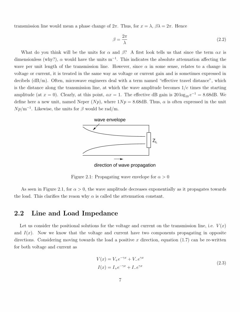
wave envelope
direction of wave propagation
Figure 2.1: Propagating wave envelope for α > 0
As seen in Figure 2.1, for α > 0, the wave amplitude decreases exponentially as it propagates towards
the load. This clarifies the reaon why α is called the attenuation constant.
2.2 Line and Load Impedance
Let us consider the positional solutions for the voltage and current on the transmission line, i.e. V (x)
and I(x). Now we know that the voltage and current have two components propagating in opposite
directions. Considering moving towards the load a positive x direction, equation (1.7) can be re-written
for both voltage and current as
V (x) = V+e−γx + V−eγx
I(x) = I+e−γx + I−eγx(2.3)
7
As seen in (2.3), there are four unknowns, i.e. V+, V−, I+ and I−. However, the current equation may
also be expressed in terms of V+ and V−. Let us see how. We will make use of the knowledge of γ as a
function of line parameters, i.e. γ2 = (R + jΩL)(G + jΩC). Consider equation (1.1), which is
dV
dx= −(R + jΩL)I
= −√
(R + jΩL)(G + jΩC)
√
R + jΩL
G + jΩCI
Observe the above expression carefully. The term√
R+jΩL
G+jΩChas the units of impedance, so let us call it
Z0. We now havedV
dx= −γZ0I (2.4)
Now let us differentiate the voltage expression in (2.3) as per the results obtained in (2.4).
−γZ0I(x) = −γV+e−γx + γV−eγx
∴ I(x) =1
Z0
(V+e−γx − V−eγx) (2.5)
In some sense, the impedance Z0 seems to govern the line voltage and current much like Ohm’s Law.
Z0 is seen to depend on the per unit length line parameters R, L, G and C, and also on the frequency
of operation Ω. Thus, Z0 is an impedance not physically present anywhere on the line, but rather, a
distributed impedance that is characteritic to the line parameters themselves. Z0 is thus called the char-
acteristic impedance of the transmission line and is a very important quantity governing microwave-based
designs.
Let us now change our analysis slightly. So far, we have now focused more on the transmission line
parameters than anything else. It will be soon clear that the load connected at the end of the line plays
a very important factor in determining the voltage and current variation along the length of the line. Let
us therefore, consider a length axis l, where l = 0 is the position of the load and movement twoards the
voltage source indicates movement along the positive l direction. Thus, substituting x = −l in (2.3) gives
us
V (l) = V+eγl + V−e−γl
I(l) = I+eγl + I−e−γl(2.6)
8
Using the results obtained in (2.5), we have
V (l) = V+eγl + V−e−γl
I(l) =1
Z0
(V+eγl − V−e−γl)(2.7)
The impedance at any point on the line is thus given by
Z(l) =V (l)
I(l)= Z0
V+eγl + V−e−γl
V+eγl − V−e−γl(2.8)
Recall that the quantities V+eγl and V−e−γl denote wave propagation in opposite directions- towards
the load and source respectively. Intuitively, we can say that the voltage component V+eγl travels towards
the load due to excitation from the source at the other end of the transmission line. However, the voltage
component V−e−γl, which travels back to the source, is not what one would have expected to exist. In
some sense, this quantity is a voltage “reflected” back from the load. Let us define a quantity Γ, called
voltage reflection coefficient, as follows
Γ(l) =V−e−γl
V+eγl=
V−
V+
e−2γl (2.9)
Thus, the reflection coefficient at any point along the line is the ratio of the backward moving wave to
the forward moving wave in terms of voltage magnitude, at that point. The original idea of designing a
transmission line is to transmit the entire power from the source to the load, without any power reflected
back from the load. Moreover, reflection towards the source can degrade the performance of the source
itself over time. Hence, we aim to have the reflection coefficient Γ as small as possible. Consider equation
(2.8), where
Z(l) = Z0V+eγl + V−e−γl
V+eγl − V−e−γl
At l = 0, i.e. at the load, we have the load impedance Z(0) = ZL = V (0)/I(0). Thus, at l = 0, taking
V+ common from both numerator and denominator,
ZL = Z01 + ΓL
1 − ΓL
(2.10)
where ΓL is the reflection coefficient at the load end. Now, ΓL can be expressed from (2.10) by
ΓL =ZL − Z0
ZL + Z0
(2.11)
9

Equation (2.11) gives some interesting information. It is clear that ΓL (subsequently, the Γ at any point
l) takes values such that 0 ≤ |Γ(l)| ≤ 1, which is true since the maximum power that can be reflected back
to the source can equal the input power itself (principle of conservation of energy). To ensure zero reflected
power, clearly the load impedance has to be equal to the line characteristic impedance, i.e. ZL = Z0. Such
a condition is known as a matched condition and is critical in ensuring that the load absorbs all the
indcident power and reflects back nothing. What happens when the load is (a) an open circuit and (b) a
short circuit?
2.3 Design Issues in Transmission Lines
So far, we have studies some important characteristics in a transmission line- the wave propagation, line
and load impedances and how they affect the wave characteristics in the line. Here, we look briefly into
certain related issues that are important for engineers who wish to design transmission lines at very high
frequencies.
2.3.1 Transmission Line Losses
We have seen that the quantity γ governs the wave propagation characteristics in terms of both ampli-
tude and phase. As γ = α + jβ, we have seen in section 2.1 that α affects the wave amplitude variation in
the line and β is related to the phase of the sinusoid. We would like the transmission line to be a lossless
line, i.e. the power that reaches the load should be the same as the power generated by the source. It
is evident that the quantity α governs the power delivered to the load. If α 6= 0, we have seen that the
wave amplitude changes (more specifically, decreases) exponentially as we move towards the load. This
directly indicates a loss; the voltage amplitude that reaches the load is not the same as that generated by
the source. Thus, for the line to be lossless, it must have α = 0.
What is the physical implication of all this? How does the fact that a lossless line having α = 0
translate physically? Let us revert to the expression for the propagation constant γ. We know that,
γ =√
(R + jΩL)(G + jΩC)
To have α = 0, as a result, we need γ = jβ. This can only happen when R = G = 0. With this, we
now have,
γ = jΩ√
LC
=⇒ β = Ω√
LC(2.12)
10

We have seen that, β = 2π/λ. Substituting in (2.12), we get
2π
λ= 2πf
√LC
The wave velocity v is the product of frequency and wavelength, which can be expressed as
v =1√LC
(2.13)
For a lossless line the characteristic impedance Z0 is purely real, since both R = G = 0. Thus,
Z0 =
√
L
C(2.14)
This indicates the physical properties of a lossless line. Resistance and conductance are lossy elements
and must be zero to minimize the losses. Since the AC impedance of R and G are frequency-independent,
these are lossy components, unlike the line inductance and capacitance.
2.3.2 Matching in Transmission Lines
We have discussed that when a line is excited by an AC source, there are voltage and current waves
traveling on the line, in both directions- to and from the load. The waves traveling back to the source are
termed as reflected waves. The waves reflected back to the source are highly undersirable as they tend to
load the source and reduces its life. Thus, the second important design consideration is matching, in order
to minimize reflections from the load.
Recall our discussion in section 2.2, where the concept of reflection coefficient Γ was introduced. It is
the ratio of the amplitudes of the reverse-going wave to the forward-going gave, at any point l along the
line. The matched condition requires that Γ = 0. From (2.9), we have,
Γ(l) = ΓLe−2γl
Since the term e−2γl is difficult to be made zero (as neither l nor γ is zero), we need to make ΓL = 0.
By definition, ΓL is the reflection coefficient at the load, which is given by (2.11), as
ΓL =ZL − Z0
ZL + Z0
11

ΓL = 0 would imply that
ZL = Z0 (2.15)
This is a very important result and is known as the matched condition. Under this condition, there will
be no reflected wave from the load to the source. The matched condition is somewhat analogous to the
maximum power transfer theorem as in circuit theory and is a highly desirable condition in the design of
transmission lines. We would like to design lossless (zero attenuation) and matched transmission lines.
2.3.3 Line Impedance Revisited
We have already derived the expressions for voltage and current as a function of position l on the
transmission line. Thus, the impedance at any point l on the line is given by (2.8) as
Z(l) = Z0V+eγl + V−e−γl
V+eγl − V−e−γl
We know that ΓL = V+/V−. Substituting, we get
Z(l) = Z0eγl + ΓLe−γl
eγl − ΓLe−γl
Also, ΓL = (ZL − Z0)/(ZL + Z0). Putting this we get
Z(l) = Z0
eγl + ZL−Z0
ZL+Z0
e−γl
eγl − ZL−Z0
ZL+Z0
e−γl
= Z0(ZL + Z0)e
γl + (ZL − Z0)e−γl
(ZL + Z0)eγl − (ZL − Z0)e−γl
= Z0ZL(eγl + e−γl) + Z0(e
γl − e−γl)
ZL(eγl − e−γl) + Z0(eγl + e−γl)
Expressing the sum of exponentials as hyperbolic cosine and sine functions, this equation becomes
Z(l) = Z0ZL cosh γl + Z0 sinh γl
ZL sinh γl + Z0 cosh γl(2.16)
Equation (2.16) is a very important result. It indicates that if we know the characteristic impedance
Z0 and the load impedance ZL, then we can calculate the impedance Z at any other point on the line l. In
fact, this can be generalized even further- if we know the characteristic impedance Z0 and the impedance
at any point on the line l1, then we can find the impedance at any other point on the line l2 6= l1! Hence,
this relation is known as the impedance transformation relation and is a very handy tool.
12

Let us now bring in a new term called normalized impedance, wherein the impedance at any point
on the line is taken with reference to Z0. Consider the impedance Z(l) whose normalized impedance is
expressed as
z(l) =Z(l)
Z0
(2.17)
As is clear, the zL term is unitless. The normalized impedance is a useful term, whose significance shall
be discussed later. In terms of this, the impedance transformation relation can be written as
z(l) =zL cosh γl + sinh γl
zL sinh γl + cosh γl(2.18)
Let us now focus our discussion on lossless transmission lines. In (2.18), we can then replace γ = α+jβ.
Doing so gives us the impedance transformation relation for lossless lines, as
z(l) =zL cos βl + j sin βl
jzL sin βl + cos βl(2.19)
Based on this, let us now examine some interesting properties of a lossless transmission line. Suppose
we know the normalized impedance on a line at point l, which is, say, z(l). Let us now move along the
length of the line by a distance λ/4, where λ is the operating wavelength. The normalized impedance at
this point is then
z(l + λ/4) =zL cos β(l + λ/4) + j sin β(l + λ/4)
jzL sin β(l + λ/4) + cos β(l + λ/4)
We know that β = 2π/λ. Putting this in the above expression, we have
z(l + λ/4) =zL cos(βl + π/2) + j sin(βl + π/2)
jzL sin(βl + π/2) + cos(βl + π/2)
=−zL sin βl + j cos βl
jzL cos βl − sin βl
Multiplying both numerator and denominator by −j, we have
z(l + λ/4) =jzL sin βl + cos βl
zL cos βl + j sin βl
=⇒ z(1 + λ/4) =1
z(l)
(2.20)
We can thus state the first result as
Result 1 The normalized line impedance inverts itself every λ/4 distance along the line.
13

Now, let us move a distance of λ/2 along the transmission line. The normalized impedance is then
z(l + λ/2) =zL cos(βl + π) + j sin(βl + π)
jzL sin(βl + π) + cos(βl + π)
=zL cos βl + j sin βl
jzL sin βl + cos βl
= z(l)
This brings us to the second result.
Result 2 The line impedance repeats itself every λ/2 distance along the line.
As far as matching is concerned, the absolute load impedance does not have much meaning by itself.
All line impedances are with respect to the characteristic impedance Z0. Hence, in many discussions in
future, we will find ourselves discussing more with the normalized impedance rather than the absolute
impedance. This brings us to another obvious, yet indispensable result.
Result 3 The normalized load impedance for a matched load is unity.
2.4 Wave Patterns in Transmission Lines
Let us now revisit the solutions for voltage and current on transmission lines as a function of the position
l. These are given by (2.7).
V (l) = V+eγl + V−e−γl
I(l) =1
Z0
(V+eγl − V−e−γl)
For lossless lines, these become
V (l) = V+ejβl + V−e−jβl
I(l) =1
Z0
(V+ejβl − V−e−jβl)(2.21)
This set of lines may be rewritten by taking the V+ejβl term common. This is done in order to find the
maximan and minima of the voltage and current along the line. Since we already know the definition of
reflection coefficient Γ,
V (l) = V+ejβl(1 + ΓLe−j2βl)
I(l) =V+
Z0
ejβl(1 − ΓLe−j2βl)(2.22)
14

The load reflection coefficient in general, may be a complex quantity depending on the load impedance
ZL. Hence ΓL can be expressed in polar form with a magnitude and a phase component as ΓL = |ΓL|ejφL .
Equation (2.22) now becomes
V (l) = V+ejβl(1 + |ΓL|ej(φL−2βl))
I(l) =V+
Z0
ejβl(1 − |ΓL|ej(φL−2βl))(2.23)
Let us focus on the voltage equation term 1 + |ΓL|ej(φL−2βl). This can be visualized as a vector sum of
a constant unit vector and a vector whose phase is decided by l. As l increases, the phase angle (φL − 2βl)
decreases, implying a clockwise rotation. Thus, as we move from the load towards the source, the vector
locus rotates clockwise. Figure 2.2 illustrates this.
1
φL− 2βl
|Γ L|
movementtowards source
AB
Figure 2.2: Locus of the vector 1 + |ΓL|ej(φL−2βl)
Clearly, the voltage maxima is achieved at point B, when (φL − 2βl) = 0 and the voltage minima is at
A, where (φL − 2βl) = π. Consequently, the current maxima and minima occur at A and B respectively
(convince yourself). Therefore, we can generalize the following in case of voltage along the line:
Voltage magnitude Phase conditionMaxima (φL − 2βl) = 2nπMinima (φL − 2βl) = (2n + 1)π
Here, n is any integer (we assume non-negative, for the sake of simplicity) i.e. nǫ0, 1, ..... We can
thus, very easily compute the magnitudes of the maximum and minimum voltages using Figure 2.2.
|Vmax| = V+ejβl(1 + |ΓL|)|Vmin| = V+ejβl(1 − |ΓL|)
(2.24)
15
Define a Voltage Standing Wave Ratio (VSWR) ρ, as
ρ =|Vmax||Vmin|
=1 + |ΓL|1 − |ΓL|
(2.25)
We know by now, that 0 ≤ |ΓL| ≤ 1, which means that 1 ≤ ρ ≤ ∞. For a perfectly matched line, the
load VSWR should be unity. This quantity VSWR is merely an extension to our knowledge of the reflection
coefficient, but is a highly useful tool for measurements at microwave frequencies. For instance, we can
very easily compute the maximum and minimum impedance along the transmission line. At the point of
maximum impedance, the voltage magnitude peaks and the current magnitude reaches a minimum. From
(2.23) and (2.24), you can show that
Zmax = ρZ0
Zmin =Z0
ρ
(2.26)
And in terms of normalized impedance, the Zmax is simply equal to the VSWR! Thus, this analysis
shows us the pattern of the standing waves along the line. Voltage and current waves are out of phase
by 180 (from the fact that voltage maxima/minima coincide with current minima/maxima respectively).
Also, consecutive maxima or minima are apart from each other by a distance of λ/2. Can you prove this?
2.5 The Smith Chart
We have seen that the impedance at any point on the line can be calculated provided we know the load
impedance and the characteristic impedance. We can also do these operations the other way round, i.e.
the load impedance can be caluclated provided we know the impedance at some other point on the line.
Such comptutations can be done by means of the impedance transformation relation. We shall, for now,
limit our discussion to lossless transmission lines i.e. α = 0. However, the computation of impedances
using the transformation relation, though straightforward, is rather tedious and non-intuitive. In this
section, we shall study a simple graphical or figurative tool, the Smith Chart, which will aid us in solving
problems on transmission lines. This tool was developed by Philip H. Smith in 1939 and is still widely in use.
Consider the normalized impedance at any point on the line, denoted as z. The reflection coefficient
at this point is then given by
Γ =z − 1
z + 1(2.27)
Recall that Γ is a complex quantity, and the expression in (2.27) indicates that every value of z can be
16

mapped into a unique value of Γ (how?). Let us then, try to map every value of normalized impedance z
onto a point in the complex-Γ plane. Let z = r + jx and Γ = u + jv. From (2.27), we have
z =1 + Γ
1 − Γ
∴ r + jx =1 + u + jv
1 − (u + jv)
=(1 + u) + jv
(1 − u) − jv
Let us rationalize the R.H.S., i.e. multiply both numerator and denominator by (1 − u) + jv.
∴ r + jx =(1 + u) + jv
(1 − u) − jv
(1 − u) + jv
(1 − u) + jv
=1 − u2 − v2 + j2v
(1 − u)2 + v2
Equating the real part of the R.H.S. to r and the imaginary part to x, we have the following equations.
r =1 − u2 − v2
(1 − u)2 + v2
x =2v
(1 − u)2 + v2
(2.28)
2.5.1 Constant Resistance Solution
Consider the resistance expression in (2.28). Since we are expressing r as a function of the complex
Γ plane axes u and v, we need to arrive at a particular expression in terms of u and v to determine the
nature of the mapping.
r =1 − u2 − v2
(1 − u)2 + v2
∴ r(1 − u)2 + rv2 = 1 − u2 − v2
∴ r − 2ru + ru2 + rv2 + u2 + v2 − 1 = 0
∴ (r + 1)u2 − 2ru + r − 1 + (r + 1)v2 = 0
Dividing throughout by (r + 1) we get
u2 − 2ru
r + 1+ v2 +
r − 1
r + 1= 0
17

Completing the square, we get
u2 − 2ru
r + 1+
(
r
r + 1
)2
+ v2 +r − 1
r + 1=
(
r
r + 1
)2
∴
(
u − r
r + 1
)2
+ v2 =
(
r
r + 1
)2
− r − 1
r + 1
∴
(
u − r
r + 1
)2
+ v2 =
(
r
r + 1
)2
− r2 − 1
(r + 1)2
∴
(
u − r
r + 1
)2
+ v2 =
(
1
r + 1
)2
(2.29)
Clearly, (2.29) shows the equation of a circle, with centre (r/(r + 1), 0) and radius 1/(r + 1). Based on
various values of the normalized resistance component r, a set of cricles can be formed, as shown in Figure
2.3. Each circle corresponds to a unique values of r and hence are called constant resistance circles. The
coordinates indicate the corresponding u- and v-values.
r = 0
r = 1
r = 2r = 3
r = ∞(0,0)(-1,0) (1/2,0)
(1,0)
Figure 2.3: Constant Resistance Circles on the Complex Γ-plane
18

2.5.2 Constant Reactance Solution
Consider the reactance expression in (2.28). Solving in a similar procedure to the constant resistance
solution, we have
x =2v
(1 − u)2 + v2
∴ x(1 − u)2 + xv2 = 2v
∴ x(1 − u)2 + xv2 − 2v = 0
Dividing by x and completing the square, we get
(u − 1)2 + v2 − 2v
x+
1
x2=
1
x2
∴ (u − 1)2 +
(
v − 1
x
)2
=
(
1
x
)2
(2.30)
Clearly, (2.30) is the equation of a circle centered at (1, 1/x) and radius 1/x. The set of constant
reactance circles which can thus be obtained are shown in Figure 2.4.
(1,0)
u = 1
x = 1
x = 2
x = 3
x = -1
x = -2
x = -3
x = -∞
x = ∞
Figure 2.4: Constant Reactance Circles on the Complex Γ-plane
The circles on the positive half of the Γ-plane correspond to the inductive reactance component whille
19

those on the negative half of the Γ-plane correspond to the capacitive reactance component. Combining
the results of the constant resistance and reactance circles, we get what is called the Smith Chart, as shown
in Figure 2.5. Simply by superimposing the resistance and reactance circles, the Smith Chart is obtained
as a result. The outermost circle points to r = 0. As an exrecise, point out the resistance and reactance
circles for discrete values.
Figure 2.5: Smith Chart as a superposition of resistance and reactance circles
Let us now see some interesting results from the Smith Chart in Figure 2.5. Consider the point
Γ = 0. This would mean that this point corresponds to z = 1, i.e. the corresponding impedance is equal
to the characteristic impedance. A short-circuit impedance, i.e. z = 0, would be the point where the
r = 0, x = 0 circles intersect, and an open-circuit impedance, i.e. z = ∞ would be the point where the
r = ∞, x = ∞ circles intersect. Thus, we see that every impedance is uniqeuly identitfied by intersection
of a constant resistance and a constant reactance circle. Recall from our discussion in section 2.4 that a
clockwise movement on the Γ-plane corresponds to movement towards the source and vice-versa (as per
our conventions on length l). Figure 2.6 shows the results.
Recall from our discussion in section 2.3.3 that the normalized line impedance inverts itself after every
λ/4 length along the line and repeats every λ/2 length along the line. This means that half the Smith
Chart circumference corresponds to a movement of λ/4 on the line, and one full circumference implies a
λ/2 movement. You can verify this easily by considering the open- and short-circuit points on the line.
Commonly used Smith Charts don’t just have a few circles- they are calibrated much like a stationery
graph sheet- with accurately labeled resistance and reactance circles. Figure 2.7 shows a commercially
available Smith Chart that is commonly used to solve transmission line problems.
20

0
z = 1
shortcircuit(z = 0)
opencircuit(z = ∞)
movementtowards source
movementtowards load
Figure 2.6: Various results using Smith Chart
Figure 2.7: A commonly used Smith Chart
21