microwave oscillator with phase noise reduction using
TRANSCRIPT

Microwave Oscillator with Phase Noise
Reduction Using Nanoscale Technology for
Wireless Systems
A thesis submitted for the degree of PhD at the University of Manchester
Faculty of Engineering and Physical Sciences
2015
MOHAMMED ALI AQEELI
SCHOOL OF ELECTRICAL AND ELECTRONIC ENGINEERING
MICROWAVE AND COMMUNICATION SYSTEMS GROUP

Microwave Oscillator with Phase Noise Reduction Using Nanoscale Technology for Wireless Systems M. Aqeeli
2
ABSTRACT
This thesis introduces, for the first time, a novel 4-bit, metal-oxide-metal (MOM) digital
capacitor switching array (MOMDCSA) which has been implemented into a wideband
CMOS voltage controlled oscillator (VCO) for 5 GHz WiMAX/WLAN applications.
The proposed MOMDCSA is added both in series and parallel to nMOS varactors. For
further gain linearity, a wider tuning range and minor phase noise variations, this
varactor bank is connected in parallel to four nMOS varactor pairs, each of which is
biased at a different voltage. Thus, VCO tuning gain reduces and optimal phase noise
variation is obtained across a wide range of frequencies. Based on this premise, a
wideband VCO is achieved with low phase noise variation of less than 4.7 dBc/Hz. The
proposed VCO has been designed using UMC 130 nm CMOS technology. It operates
from 3.45 GHz to 6.23 GHz, with a phase noise of -133.80 dBc/Hz at a 1 MHz offset, a
figure of merit (FoM) of -203.5 dBc/Hz.
A novel microstrip low-phase noise oscillator is based on a left-handed (LH)
metamaterial bandpass filter which is embedded in the feedback loop of the oscillator.
The oscillator is designed at a complex quality factor Qsc peak frequency, to achieve
excellent phase noise performance. At a centre frequency of 2.05 GHz, the reported
oscillator demonstrates, experimentally, a phase noise of -126.7 dBc/Hz at a 100 kHz
frequency offset and a FoM of -207.2 dBc/Hz at a 1 MHz frequency offset.
The increasing demands have been placed on the electromagnetic compatibility
performance of VCO devices is crucial. Therefore, this thesis extends the potential of
highly flexible and conductive graphene laminate to the application of electromagnetic
interference (EMI) shielding. Graphene nanoflake-based conductive ink is printed on
paper, and then it is compressed to form graphene laminate with a conductivity of
0.43×10⁵ S/m. Shielding effectiveness is experimentally measured at above 32 dB as
being between 12GHz and 18GHz, even though the thickness of the graphene laminate
is only 7.7µm. This result demonstrates that graphene has great potential for offering
lightweight, low-cost, flexible and environmentally friendly shielding materials which
can be extended to offering required shielding from electromagnetic interference (EMI),
not only for VCO phase noise optimisation, but also for sensitive electronic devices.

Microwave Oscillator with Phase Noise Reduction Using Nanoscale Technology for Wireless Systems M. Aqeeli
3
Declaration
No portion of the work referred to in the thesis has been submitted in support of an
application for another degree or qualification of this or any other university or other
institute of learning.

Microwave Oscillator with Phase Noise Reduction Using Nanoscale Technology for Wireless Systems M. Aqeeli
4
Copyright Statement
The author of this thesis (including any appendices and/or schedules to this thesis) owns
certain copyright or related rights in it (the “Copyright”), and he has given The
University of Manchester rights to use such Copyright for administrative purposes.
Copies of this thesis, either in full or in extracts, and whether in hard or electronic copy,
may be made only in accordance with the Copyright, Designs and Patents Act 1988
(as amended) and regulations issued under it or, where appropriate, in accordance with
licensing agreements which the University has from time to time. This page must form
part of any such copies made.
The ownership of certain Copyright, patents, designs, trademarks and other intellectual
property (the “Intellectual Property”) and any reproductions of copyright works in the
thesis, for example graphs and tables (“Reproductions”), which may be described in this
thesis, may not be owned by the author and may be owned by third parties. Such
Intellectual Property and Reproductions cannot and must not be made available for use
without the prior written permission of the owner(s) of the relevant Intellectual Property
and/or Reproductions.

Microwave Oscillator with Phase Noise Reduction Using Nanoscale Technology for Wireless Systems M. Aqeeli
5
Acknowledgements
Although this report is my own work, it would not have been possible to complete it
without the help of other people. Let this paragraph be my way of thanking those who
contributed or supported me along the way. All you can see in this report would not be
possible without Dr. Zhirun Hu, the project supervisor, who gave me a chance to work
at the University of Manchester and was both supportive and motivational. I do not
recall exactly how many times he convinced me to produce high-quality publications,
but he was right – it was all worth it. Numerous times he provided me with constructive
criticism, and he also acted as the main editor of this report. I would like to thank him
for making this work and report happen. Next, I would like to thank my mother and my
father. Many years ago they convinced me and supported me to work hard. This, I
believe, helped me to become one of the best students in my class and subsequently led
me to start the doctoral programme. Thank you very much to all of my family and
friends who supported me along the way. I thank all of you for everything. Finally, I
would like to thank Professor Ali Rezazadeh, Professor Krikor Ozanyan (Head of
Sensing, Imaging and Signal Processing), Dr. Robin Sloan, Head of the Microwave and
Communication Systems (MCS) Research Group, and all of my colleagues and friends
for all their help and support.
Microwave Oscillator with Phase Noise Reduction Using Nanoscale Technology for Wireless Systems M. Aqeeli
6
Figures list
Figure 1.1 Bock diagram of a typical heterodyne receiver ............................................. 34
Figure 1.2 Block diagram of basic phase-locked loop .................................................... 36
Figure 1.3 PLL linear model ........................................................................................... 37
Figure 1.4 Passive loop filter model ............................................................................... 38
Figure 1.5 Desired operation regions for a VCO tuning curve. ..................................... 42
Figure 1.6 Phase noise of VCOs with accumulation-mode nMOS, inversion mode
pMOS and varactor diode. .............................................................................................. 48
Figure 2.1 An ideal signal (left) and an actual signal with additional phase
noise (right) .................................................................................................................... 64
Figure 2.2 Phase noise definition .................................................................................... 67
Figure 2.3 Sidebands around the carrier as a result of AM (a) and PM (b) .................... 69
Figure 2.4 VCO phase noise characteristics: (a) Low-Q (b) High-Q ............................. 70
Figure 2.5 Noise attributes of a MOSFET transistor in a fixed bias condition .............. 71
Figure 2.6 The open-loop transfer function .................................................................... 72
Figure 2.7 Signal path phase noise model ...................................................................... 75
Figure 2.8 Block diagram of a PLL system .................................................................... 81
Figure 2.9 Leeson’s Phase Noise Model ........................................................................ 88

Microwave Oscillator with Phase Noise Reduction Using Nanoscale Technology for Wireless Systems M. Aqeeli
7
Figure 2.10 Phase noise model of an LC feedback oscillator with low fm or low Q0. ... 91
Figure 2.11 Phase noise model of an LC feedback oscillator with high fm or high Q0.. 91
Figure 2.12 The effect of phase noise on wireless receivers .......................................... 95
Figure 2.13 The effect of phase noise on the transmit path. The nearby transmitter’s
phase noise might overwhelm the weak wanted signal .................................................. 95
Figure 3.1 Direct conversion receiver for multi-standard cellular application ............. 100
Figure 3.2 Receiver architectures for WLAN applications at the 2.4 GHz ISM band . 101
Figure 3.3 An integer-N PLL frequency synthesiser architecture ................................ 102
Figure 3.4 (a) CP and VCO connection through a loop filter (b) Desired operating
region for a VCO tuning curve ..................................................................................... 109
Figure 3.5 Different approaches to a broadband VCO with sub-bands: (a) a capacitance
switching LC tank and (b) an inductance switching LC tank ....................................... 111
Figure 3.6 Different approaches to the broadband VCO with switching between LC
tanks [1] ........................................................................................................................ 112
Figure 3.7 nMOS transistors as an RF switch: (a) VSW is low, in the OFF state, while
(b) VSW is high, in the ON state .................................................................................. 115
Figure 3.8 Differential capacitance switching .............................................................. 116
Figure 3.9 Differential capacitance switching with biasing resistors ........................... 116
Figure 3.10 nMOS VCO topology ................................................................................ 118

Microwave Oscillator with Phase Noise Reduction Using Nanoscale Technology for Wireless Systems M. Aqeeli
8
Figure 3.11 pMOS VCO topology ................................................................................ 119
Figure 3.12 NMOS-pMOS VCO topology ................................................................... 120
Figure 3.13 Amplitude correction circuit with detector ............................................... 123
Figure 3.14 Amplitude correction based on tuning curve selection ............................. 123
Figure 3.15 Bias filtering (a) conventional low-pass bias filter (b) nMOS bias filter .. 124
Figure 3.16 Bias filtering (a) power-up delay circuit (b) dynamic delay circuit .......... 125
Figure 3.17 Different types of on-chip inductors: a symmetric centre-tapped octagonal
spiral, a square spiral with a crossover and a circular spiral ......................................... 127
Figure 3.18 Square-shaped planar spiral inductors, w is the width of the spiral and s is
the spacing between the turns of the spiral ................................................................... 129
Figure 3.19 The use of π in the model circuit of the inductor. ..................................... 129
Figure 3.20 The simplified inductor π model circuit for the planar on-chip inductor. 130
Figure 3.21 The π- equivalent circuit for a two-port network ...................................... 138
Figure 3.22 Two methods for reducing the π-network: (a) single-ended and
(b) differential configurations ....................................................................................... 139
Figure 4.1 Mobility of electrons and holes in bulk silicon at T=300............................ 144
Figure 4.2 Resistivity of bulk silicon versus doping concentration ............................. 144
Figure 4.3 nMOS transistor on a P-type silicon waver ................................................. 148
Figure 4.4 nMOS transistor on a P-type silicon waver ................................................. 149
Microwave Oscillator with Phase Noise Reduction Using Nanoscale Technology for Wireless Systems M. Aqeeli
9
Figure 4.5 nMOS transistor on a P-type silicon waver ................................................. 150
Figure 4.6 I-V static characteristic of an MOS transistor. ............................................ 151
Figure 4.7 nMOS transistor in the saturation region .................................................... 156
Figure 4.8 Large signal equivalent circuit of an MOS transistor .................................. 159
Figure 4.9 Gate capacitances of the VGS voltage ........................................................ 161
Figure 4.10 Small signal equivalent circuit of an nMOS transistor .............................. 162
Figure 4.11 Integrated resistor in n-well ....................................................................... 167
Figure 4.12 Cross-section of integrated resistances: (a) diffusion into a well
(b) diffusion .................................................................................................................. 168
Figure 4.13 Cross-section of integrated resistances: (a) well (b) pinched well ............ 169
Figure 4.14 Cross-section of a polysilicon integrated resistance .................................. 170
Figure 4.15 Cross-section of integrated resistances with well shielding ...................... 170
Figure 4.16 Undercut effect and its boundary dependence ......................................... 172
Figure 4.17 The temperature in the centre of the resistors is: (a) dissimilar and
(b) similar ...................................................................................................................... 173
Figure 5.1 Cross-section of an nMOS varactor ............................................................ 179
Figure 5.2 Capacitance performances between the gate and the substrate with the
gate-to-source voltage ................................................................................................... 179

Microwave Oscillator with Phase Noise Reduction Using Nanoscale Technology for Wireless Systems M. Aqeeli
10
Figure 5.3 Simulated nMOS varactors with source, drain and bulk connected to the
tuning voltage ............................................................................................................... 180
Figure 5.4 Typical capacitance curve of an nMOS varactor with source, drain and bulk
connected to the tuning voltage .................................................................................... 180
Figure 5.5 Typical capacitance curves of an nMOS varactor with its source, drain and
bulk connected to the tuning voltage at different biasing gate voltages ....................... 181
Figure 5.6 nMOS varactor working in accumulation mode ......................................... 182
Figure 5.7 An nMOS varactor working in depletion mode .......................................... 183
Figure 5.8 nMOS varactor working in inversion mode ................................................ 184
Figure 5.9 Simulated nMOS varactors with source and drain connected to
the tuning voltage and bulk connected to the ground ................................................... 185
Figure 5.10 Capacitance of the nMOS varactor in inversion mode .............................. 185
Figure 5.12 Two operating modes of an nMOS varactor ............................................. 187
Figure 5.13 Influence of the operating mode ................................................................ 188
Figure 5.14 Impact of gate length of an nMOS varactor with tuning voltage .............. 189
Figure 5.15 Scalability of nMOS varactors in the inversion mode .............................. 190
Figure 6.1 Phase noise of VCOs with a body-biased pMOS varactor ........................ 193
Figure 6.2 Schematic diagram of the proposed 5.0 GHz 130 nm CMOS DCSA and its
logic control with a varactor bank ................................................................................ 196
Microwave Oscillator with Phase Noise Reduction Using Nanoscale Technology for Wireless Systems M. Aqeeli
11
Figure 6.3 Layout of the proposed differential inductor ............................................... 198
Figure 6.4 Equivalent differential inductor model ........................................................ 198
Figure 6.5 Comparison of the Q factor and resonance frequency between a single-ended
and a differential inductor ............................................................................................. 200
Figure 6.6 Inductor values and quality factor of the centre-tapped differential inductor
versus frequency ........................................................................................................... 201
Figure 6.7 Small signal equivalent circuit of the VCO ................................................. 201
Figure 6.8 KVCO and phase noise of the proposed VCO with DCSA connected in parallel
to the varactor bank. ...................................................................................................... 206
Figure 6.9 KVCO and phase noise of the proposed VCO with DCSA connected in series
and in parallel to the varactor bank ............................................................................... 211
Figure 6.10 Tuning curves of an I-MOS varactor at different biasing voltages and the
proposed design ............................................................................................................ 213
Figure 6.11 Proposed tuning circuit, including MOMDCSA with nMOS DSVB and its
logic control .................................................................................................................. 214
Figure 6.12 Layout of the VCO with a die area of 720× 586 μm2 ............................... 218
Figure 6.13 KVCO and phase noise of the proposed VCO using MOMDCSA, an nMOS
varactor pair and DSVB as the functions of control codes ........................................... 219
Figure 6.14 Oscillation frequency characteristics versus tuning voltage ..................... 219

Microwave Oscillator with Phase Noise Reduction Using Nanoscale Technology for Wireless Systems M. Aqeeli
12
Figure 6.15 Tuning characteristics and FoM of the proposed VCO MOMDCSA in series
and parallel to a varactor with a gain-linearised DSVB varactor bank ........................ 220
Figure 6.16 Phase noise performance of the proposed VCO using MOMDCSA in series
and parallel to a varactor with a gain-linearised varactor bank at a 1 MHz offset ....... 221
Figure 6.17 Phase noise variation against temperature in degrees Celsius (°C)........... 222
Figure 7.1 Figure Permittivity-permeability (ε- µ) diagram ......................................... 237
Figure 7.2 An LH MTM consisting of square split resonators and copper wire
strips .............................................................................................................................. 237
Figure 7.3 The “incremental circuit model for a hypothetical uniform LH TL” .......... 238
Figure 7.4 Characteristics of CRLH TL (a) Circuit model for unit cell TL
(b) Dispersion diagram for the CRLH, PLH, PRH structures ...................................... 240
Figure 7.5 Layout of an MTM TL unit cell based on CSRR ....................................... 242
Figure 7.6 Equivalent circuit model for the MTM TL unit cell based on CSRR ........ 243
Figure 7.7 Layout of the bandpass filter combining one right-handed and two
left-handed SRR-based coplanar unit cells ................................................................... 243
Figure 7.8 Simulated frequency response of the bandpass filter ................................. 244
Figure 7.9 The layout of a UWB bandpass filter based on CSRR balanced unit
cells ............................................................................................................................... 244
Figure 7.10 Simulated performance of the UWB bandpass filter ................................ 245

Microwave Oscillator with Phase Noise Reduction Using Nanoscale Technology for Wireless Systems M. Aqeeli
13
Figure 7.11 Top and bottom views of the open split ring resonator connected to
a microstrip line ............................................................................................................ 246
Figure 7.12 Top and bottom views of the DOSRR ...................................................... 248
Figure 7.13 Feedback oscillator. .................................................................................. 249
Figure 7.14 Layout of a four-pole elliptic filter ........................................................... 253
Figure 7.15 (a) Layout of an MTM TL unit cell based on CSRR (b) Equivalent circuit
model for the MTM TL unit cell based on CSRR ........................................................ 254
Figure 7.16 Simulated s-parameter results for the hybrid unit cell ............................. 255
Figure 7.17 Real part of permittivity and permeability for the proposed BPF ........... 256
Figure 7.18 Simulated electrical field at the resonance frequency for one unit cell .... 257
Figure 7.19 Simulated magnetic field at the resonance frequency for one unit cell .... 257
Figure 7.20 Simulated group delay results for the hybrid unit cell ............................. 258
Figure 7.21 Simple CSRR based Filter ........................................................................ 259
Figure 7.22 Simulated results of S21 for the proposed filter and simple structure ..... 259
Figure 7.23 Simulated phase response for the proposed filter and simple CSRR
filter ............................................................................................................................... 260
Figure 7.24 Layout of the proposed LH BPF .............................................................. 261
Figure 7.25 Simulated S21 results for a narrowband BPF based on one and two unit
cells ............................................................................................................................... 261

Microwave Oscillator with Phase Noise Reduction Using Nanoscale Technology for Wireless Systems M. Aqeeli
14
Figure 7.26 Simulated group delay results for the BPF using two hybrid unit cells ... 262
Figure 7.27 Complex quality factor for the BPF using two hybrid unit cells.............. 262
Figure 7.28 Complex quality factor and group delay for the BPF using two hybrid unit
cells ............................................................................................................................... 263
Figure 7.29 Amplifier used in the oscillator design .................................................... 266
Figure 7.30 Schematics of the filter with the amplifier, parts of connecting lines ...... 267
Figure 7.31 Phase response of the amplifier with the filter and parts of connecting
lines ............................................................................................................................... 267
Figure 7.32 Schematics diagram of the proposed filter based oscillator ..................... 268
Figure 7.33 Schematic of the oscillator designed at Qsc peak frequency ................... 269
Figure 7.34 Simulated harmonics for a filter-based oscillator at Qsc peak frequency . 270
Figure 7.35 Simulated phase noise for a filter-based oscillator at Qsc peak ................ 270
Figure 7.36 Schematic of the proposed oscillator, designed and implemented at group
delay peak frequency .................................................................................................... 271
Figure 7.37 Simulated output spectrum and phase noise for the oscillator designed at
group delay peak frequency .......................................................................................... 272
Figure 7.38 Simulated phase noise for the filter-based oscillator at group delay peak
frequency ...................................................................................................................... 272
Figure 7.39 Layout of the proposed feedback oscillator ............................................. 273

Microwave Oscillator with Phase Noise Reduction Using Nanoscale Technology for Wireless Systems M. Aqeeli
15
Figure 7.40 Circuit photograph of the oscillator designed at Qsc peak frequency ...... 273
Figure 7.41 Measured output spectrum of the proposed oscillator .............................. 274
Figure 7.42 Measured and simulated phase noise for the L-band oscillator .............. 275
Figure 8.1 C60 fullerene molecules, carbon nanotubes, and graphite formed from
graphene sheets ............................................................................................................. 281
Figure 8.2 Carbon atoms bonded in a honeycomb crystal lattice in graphene ......... 283
Figure 8.3 Interference injection path in a super-heterodyne receiver ...................... 284
Figure 8.4 Processes involved in preparing the graphene nanoflake-based EMI
shielding material .......................................................................................................... 288
Figure 8.5 Graphene samples and measurement of SE in a waveguide system ........... 290
Figure 8.6 Measured transmissions in a waveguide, with and without DUT ............... 291
Figure 8.7 Shielding effectiveness of graphene laminate ............................................. 292
Microwave Oscillator with Phase Noise Reduction Using Nanoscale Technology for Wireless Systems M. Aqeeli
16
List of Tables
Table 2-1 Statistical measure for different types of phase noise ..................................... 86
Table 4-1 Physical properties of silicon ....................................................................... 143
Table 4-2 Resistors feature ........................................................................................... 174
Table 6-1 Geometry of the differential inductor ........................................................... 199
Table 6-2 EM-simulated results of the inductor ........................................................... 199
Table 6-3 A comparison of the two VCOs, one with MOMDCSA in parallel to a pMOS
varactor bank and the second with MOMDCSA in parallel to a gain-linearised nMOS
varactor bank ................................................................................................................. 207
Table 6-4 A comparison of the two VCOs, one with MOMDCSA in parallel to a gain-
linearised nMOS varactor bank and the second with MOMDCSA in series and parallel
to a varactor bank .......................................................................................................... 212
Table 6-5 Working mode of the varactor bank ............................................................. 215
Table 6-6 A comparison between the three proposed VCOs ........................................ 222
Table 6-7 Performance comparison of CMOS VCOs .................................................. 226
Table 8-1 Performance comparison between published oscillators and this study ...... 277
Table 8-1Resistivity and conductivity of as-deposited and various compressed graphene
laminates. ...................................................................................................................... 287

Microwave Oscillator with Phase Noise Reduction Using Nanoscale Technology for Wireless Systems M. Aqeeli
17
Abbreviations and Symbols
Degree centigrade
∆f Frequency offset
∆f3dB 3dB-bandwidth
µ Permeability
µ0 Permeability of vacuum
ADE Analogue design environment
ADS Advanced design system
an Coefficient
BJT Bipolar junction transistor
bn Coefficient
BPF Band pass filter
BW Bandwidth
C Capacitor
C0 Overlap capacitance
CAD Computer aided design
Cctr Capacitance tuning range
Cd Depletion capacitance
Cf Fringing capacitance in varactors
Cf,fix Fixed fringing capacitance
Cf,var Variable fringing capacitance
Cjd Junction capacitance
Cmax Maximum varactor capacitance
Cmin Minimum varactor capacitance
CMODE Combining multi-objective optimization with differential evolution
Co
Microwave Oscillator with Phase Noise Reduction Using Nanoscale Technology for Wireless Systems M. Aqeeli
18
CMOS Complementary metal–oxide–semiconductor
Cox Gate oxide capacitance of varactor
Cp Parasitic capacitance
Cpc Parasitic capacitances of the VCO circuit
CRLH Composite right/left-handed
CRT Cathode ray tube
CSRR Complementary split ring resonator
Cv Variable capacitance
Cvar,max Maximum variable varactor capacitance
Cvar,min Minimum variable varactor capacitance
dB Decibels
dBc Decibels relative to the carrier
dBm Decibels to one milliwatt
DFT Discrete Fourier transform
DGS Defected ground structure
f Frequency
F Excess noise factor
f0 Center frequency of the VCO
f0 Signal frequency in Hz
FBW Fractional bandwidth
fc The 1/f corner frequency
FDM Frequency domain measurement
FET Field effect transistor
FFT Fast Fourier transform
FIF Amplifier frequency in Hz
fm The offset from the output frequency (Hz)
Microwave Oscillator with Phase Noise Reduction Using Nanoscale Technology for Wireless Systems M. Aqeeli
19
FoM Figure of merit
fres Resonance frequency
FS Signal frequency in Hz
ftr Frequency tuning range
FVCO VCO frequency in Hz
gbise Refers to the current source trans-conductance
HTS High-temperature superconductor
I/O Input/output
IC Integrated circuit
IF Intermediate frequency
k Boltzmann's constant
KVCO Sensitivity of VCO frequency to variations in Vtune
KVdd Sensitivity of VCO frequency to variations in
L Inductance
L(fm) Defines the ratio of power in a 1 Hz bandwidth
lf Finger length
lg Gate length
LO Local oscillator
Lp Parasitic inductance
LPF Low pass filter
LTCC Low-temperature co-fired ceramics
mA Milliamperes
MMIC Monolithic microwave integrated circuit
mSec Millisecond
MSRR Multiple split ring resonator
MTM Metamaterials

Microwave Oscillator with Phase Noise Reduction Using Nanoscale Technology for Wireless Systems M. Aqeeli
20
n Order of harmonic oscillation
NMOS Negative metal–oxide–semiconductor
PLL Phase-locked loop
Ploss Power consumption
PMOS Positive metal–oxide–semiconductor
PN Phase noise
Psig Signal power
Q Quality factor
Qacc Charge in accumulation layer
Qav Averaged quality factor
Qav,min Minimum averaged quality factor
QBW Quality factor according to the bandwidth
Qdep Charge in depletion layer
Qg Charge at gate node
QLC Quality factor of LC-tank
Qmin Minimum quality factor
Racc Resistance of the accumulation layer
RF Radio frequency
RF Radio frequency
Rg Gate resistance
Rinv Resistance of the inversion layer
Rp Parasitic resistance
Rs Series resistance
Rsub Substrate resistance
Rv Variable resistance
Rw Well resistances

Microwave Oscillator with Phase Noise Reduction Using Nanoscale Technology for Wireless Systems M. Aqeeli
21
SRR Split ring resonator
SSRR Symmetrical split ring resonator
T Temperature
T Period of the signal
TEM Transverse electromagnetic
TL Transmission line
tox Gate oxide thickness
VCO Voltage controlled oscillator
Vdd Supply voltage
Veff Effective voltage across gate oxide and depletion region
Veff,a,d Effective voltages for accumulation, depletion
VFB Flatband voltage
Vgate Gate voltage
Vth Threshold voltage
Vtune Tuning voltage
Vwell Well voltage
Wd Width of depletion region
Wf Finger width
Wg Gate width
α Attenuation constant
β Propagation constant
γ Complex propagation constant
ε Electric permittivity
εo Permittivity of vacuum
εox Dielectric constant of silicon dioxide
εsi Dielectric constant of silicon

Microwave Oscillator with Phase Noise Reduction Using Nanoscale Technology for Wireless Systems M. Aqeeli
22
θ Electrical length
λ Wavelength
μm Micrometre
τ Life time of charge carriers
τ Time delay
ω Angular frequency

Microwave Oscillator with Phase Noise Reduction Using Nanoscale Technology for Wireless Systems M. Aqeeli
23
Contents
Abstract 2
Dedication 3
Copy Statements 4
Acknowledgments
List of Figures
5
6
List of Tables 1 16
Abbreviations and Symbols 1 17
INTRODUCTION ................................................................................... 32 CHAPTER 1:
1.1: RF COMMUNICATION SYSTEMS ....................................................................... 32
1.2: PLL FUNDAMENTALS ...................................................................................... 36
1.3: VCOS .............................................................................................................. 40
1.4: MOM CAPACITORS ......................................................................................... 44
1.5: LITERATURE REVIEW ....................................................................................... 46
1.6: MOTIVATION AND RESEARCH OBJECTIVES ...................................................... 51
1.7: PROBLEM STATEMENT ..................................................................................... 54
1.8: THESIS ORGANISATION .................................................................................... 56
1.9: MAIN CONTRIBUTIONS .................................................................................... 59

Microwave Oscillator with Phase Noise Reduction Using Nanoscale Technology for Wireless Systems M. Aqeeli
24
1.10: CHAPTER SUMMARY ........................................................................................ 61
FUNDAMENTALS OF PHASE NOISE IN ELECTRICAL OSCILLATORS .. 62 CHAPTER 2:
2.1: INTRODUCTION ................................................................................................ 62
2.2: PHASE NOISE SPECIFICATIONS ......................................................................... 65
2.3: CHARACTERISTICS OF OSCILLATOR NOISE ....................................................... 70
2.4: QUALITY FACTOR AND NOISE IN LC VCO ....................................................... 71
2.4.1: Quality factor .............................................................................................. 71
2.4.2: Dependence of phase noise on the offset frequency and the Q factor ........ 75
2.5: PHASE NOISE IN OFDM WIRELESS SYSTEMS ................................................... 78
2.5.1: Free-Running Oscillator ............................................................................. 80
2.5.1.1: Oscillator With PLLs ....................................................................... 81
2.5.1.2: First order PLL: ............................................................................... 82
In this model F(s)=1 and the closed loop transfer function is given by: ........... 82
2.5.1.3: Second –order PLLB ........................................................................ 84
2.6: PHASE NOISE MODELS ..................................................................................... 86
2.6.1: Leeson’s time-invariant (LTI) phase noise model ...................................... 87
2.6.2: Time-variant (TV) Hajimiri and Lee model. .............................................. 92
2.6.3: Design implications and limitations of the Hajimiri-Lee model ................ 93
2.7:THE EFFECT OF PHASE NOISE IN WIRELESS COMMUNICATION AND RADAR SYSTEMS 94

Microwave Oscillator with Phase Noise Reduction Using Nanoscale Technology for Wireless Systems M. Aqeeli
25
2.8: PHASE NOISE MEASUREMENT .......................................................................... 96
2.9: CHAPTER SUMMARY ........................................................................................ 97
SYSTEM DESIGN CONSIDERATION OF WIDEBAND VCOS ................. 99 CHAPTER 3:
3.1: INTRODUCTION ................................................................................................ 99
3.2: RADIO ARCHITECTURE AND FREQUENCY PLANNING CONSIDERATIONS .......... 100
3.3: THE PROBLEM OF SPECTRAL PURITY .............................................................. 103
3.4: FM NOISE CONTRIBUTIONS ............................................................................ 104
3.5: AM-FM CONVERSION NOISE CONTRIBUTION ................................................ 105
3.6: SPURIOUS SIDEBANDS ................................................................................... 107
3.7: SUPPLY VOLTAGE EFFECTS ............................................................................ 108
3.8: CONSIDERATION OF CIRCUIT DESIGN AND IMPLEMENTATION ........................ 110
3.8.1: Wideband VCO implementing sub-bands ................................................ 111
3.8.2: Switching techniques for a wideband LC-VCO ....................................... 113
3.8.2.1: Capacitance switching ................................................................... 113
3.8.2.2: Inductance switching ..................................................................... 117
3.9: WIDEBAND VCO IMPLEMENTATION ............................................................. 118
3.9.1: Active circuit design ................................................................................. 118
3.9.2: Programmable bias current ....................................................................... 122

Microwave Oscillator with Phase Noise Reduction Using Nanoscale Technology for Wireless Systems M. Aqeeli
26
3.9.3: Bias noise filtering .................................................................................... 124
3.10: LC TANK DESIGN ........................................................................................... 126
3.10.1: Spiral inductor modelling ......................................................................... 128
3.10.2: Quality factor of inductors ........................................................................ 132
3.10.2.1: Instantaneous quality factor ........................................................... 133
3.10.3: Layout of spiral inductor .......................................................................... 134
3.10.4: Losses in spiral inductors ......................................................................... 135
3.10.5: Inductor circuit models ............................................................................. 137
3.11: CHAPTER SUMMARY ...................................................................................... 141
CMOS TRANSISTORS ....................................................................... 142 CHAPTER 4:
4.1: MATERIAL PROPERTIES ................................................................................. 142
4.1.1: Silicon ....................................................................................................... 142
4.1.1.1: Silicon dioxide ............................................................................... 145
4.1.1.2: Polysilicon ..................................................................................... 146
4.2: CMOS TECHNOLOGY ................................................................................... 146
4.2.1: The characterisation of the I-V curve ....................................................... 148
4.2.2: Weak inversion region .............................................................................. 151
4.2.3: Triode region ............................................................................................ 153
4.2.4: Saturation region ...................................................................................... 155

Microwave Oscillator with Phase Noise Reduction Using Nanoscale Technology for Wireless Systems M. Aqeeli
27
4.3: EQUIVALENT CIRCUITS IN A CMOS TRANSISTOR .......................................... 159
4.3.1: Large signal equivalent circuit ................................................................. 159
4.3.2: Small signal equivalent circuit ................................................................. 162
4.4: CADENCE VIRTUOSO ANALOGUE DESIGN ENVIRONMENT ............................... 165
4.5: CMOS RESISTORS AND CAPACITORS ............................................................. 167
4.5.1: Integrated resistors .................................................................................... 167
4.5.2: Integrated resistor accuracy ...................................................................... 170
4.6: CHAPTER SUMMARY ...................................................................................... 174
MOS VARACTOR DESIGN ................................................................ 175 CHAPTER 5:
5.1: PRINCIPLES OF NMOS VARACTORS ............................................................... 177
5.1.1: Accumulation mode varactors .................................................................. 181
5.1.2: Depletion mode varactors ......................................................................... 182
5.1.3: Inversion mode varactors ......................................................................... 183
5.2: OPERATING MODE INFLUENCE ON AN NMOS VARACTOR .............................. 187
5.2.1: Influence of the geometrical parameters on an nMOS varactor ............... 188
5.2.1.1: Influence of gate length variations ................................................ 188
5.2.1.2: Impact of variations in varactor size ............................................. 189
5.3: CHAPTER SUMMARY ...................................................................................... 190

Microwave Oscillator with Phase Noise Reduction Using Nanoscale Technology for Wireless Systems M. Aqeeli
28
DIGITALLY CONTROLLED MICROWAVE VCO WITH A WIDE TUNING CHAPTER 6:
RANGE AND LOW PHASE NOISE VARIATION ............................................................. 191
6.1: INTRODUCTION .............................................................................................. 191
6.2: CIRCUIT DESIGN AND IMPLEMENTATION ....................................................... 194
6.2.1: Integrated spiral inductor .......................................................................... 196
6.2.2: Varactor for low phase noise variation ..................................................... 201
6.2.2.1: MOMDCSA in parallel with a gain-linearised varactor ................ 203
6.2.2.2: MOMDCSA in series and parallel to a varactor bank ................... 207
6.2.2.3: MOMDCSA in series and parallel to a varactor with gain linearized
varctor bank ..................................................................................................... 212
6.3: SIMULATION RESULTS ................................................................................... 217
6.4: CHAPTER SUMMARY ...................................................................................... 223
LOW PHASE NOISE MICROWAVE OSCILLATOR BASED ON A CHAPTER 7:
MINIATURISED META-MATERIAL BANDPASS FILTER ............................................... 231
7.1: INTRODUCTION TO CST ................................................................................ 234
7.2: FUNDAMENTALS OF LEFT-HANDED METAMATERIALS .................................... 235
7.3: TRANSMISSION LINE APPROACH .................................................................... 238
7.4: COMPOSITE RIGHT-/LEFT-HANDED (CRLH) TL ............................................ 240
7.5: METAMATERIAL FILTERS .............................................................................. 241

Microwave Oscillator with Phase Noise Reduction Using Nanoscale Technology for Wireless Systems M. Aqeeli
29
7.6: FEEDBACK OSCILLATOR ................................................................................ 249
7.7: OSCILLATOR DESIGN USING AN LH BANDPASS FILTER .................................. 251
7.8: FILTER DESIGN USING LH TRANSMISSION LINE UNIT CELLS........................... 253
7.9: OSCILLATOR DESIGN AT QSC AND THE GROUP DELAY PEAK FREQUENCY ....... 265
7.10: CHAPTER SUMMARY ...................................................................................... 277
ELECTROMAGNETIC INTERFERENCE SHIELDING BASED ON HIGHLY CHAPTER 8:
FLEXIBLE AND CONDUCTIVE GRAPHENE LAMINATE ............................................... 279
8.1: INTRODUCTION .............................................................................................. 279
8.2: THE RISE OF GRAPHENE ................................................................................. 280
8.3: EFFECT OF LOW- AND HIGH-POWER CONTINUOUS WAVE ELECTROMAGNETIC
INTERFERENCE ON A MICROWAVE VCO ....................................................................... 283
8.4: GRAPHENE-BASED EMI SHIELDING ............................................................... 284
8.5: ELECTROMAGNETIC INTERFERENCE SHIELDING BASED ON HIGHLY CONDUCTIVE
GRAPHENE LAMINATE .................................................................................................. 285
8.6: CHAPTER SUMMARY ...................................................................................... 293
CONCLUSION AND FUTURE WORK ................................................... 294 CHAPTER 9:
9.1: CONCLUSION ................................................................................................. 294
9.2: FUTURE RESEARCH OPPORTUNITIES .............................................................. 297
LIST OF PUBLICATIONS ............................................................................................... 299

Microwave Oscillator with Phase Noise Reduction Using Nanoscale Technology for Wireless Systems M. Aqeeli
30
REFERENCES . …………………………………………………………………….302
Microwave Oscillator with Phase Noise Reduction Using Nanoscale Technology for Wireless Systems M. Aqeeli
31
Appendices
A COMPARISON OF INDUCTOR'S QUALITY FACTOR, SERIES RESISTANCE AND
FREQUENCY AT DIFFERENT THICKNESS. ....................................................................... 321
B UMC 130NM NMOS TRANSISTORS STANDARD PERFORMANCE ENHANCEMENT
1.2 V USING CADENCEVIRTOUSO ................................................................................ 325
C METAL-OXIDE-METAL CAPACITOR DEVICE ARCHITECTURE. ........................ 329
D VCO GAIN AND TUNING FREQUENCY VERSUS DIGITAL SWITCHING VARACTOR
BANK AS THE FUNCTIONS OF CONTROL VOLTAGE. ........................................................ 330

Microwave Oscillator with Phase Noise Reduction Using Nanoscale Technology for Wireless Systems M. Aqeeli
32
Introduction Chapter 1:
1.1: RF communication systems
Voltage-controlled oscillators (VCOs) are critical components of RF circuits used in
transmitters, receivers, frequency synthesisers and signal-tracking generators as sources
of carrier waves with tuneable frequencies. The rapid development of microelectronic
circuits has led to a huge amount of research on the integrated implementation of
oscillator circuits. Combining a wideband tuning range with fixed phase noise is not
possible. There has to be differences in phase noise values (variations) across the
bandwidth and still one of the most challenging challenges in the design of LC-VCOs,
as the VCO must achieve a high degree of spectral purity.
The rapid, explosive and tremendous growth of telecommunications applications has
brought increasing demand for sophisticated, low-cost and high-performance radio
frequency integrated circuits (RFICs). Wireless communication consists of important
building blocks known as ‘phase-locked loop (PLL) frequency synthesisers’ [1]. A very
important and critical element of almost any PLL frequency synthesiser or transceiver
Microwave Oscillator with Phase Noise Reduction Using Nanoscale Technology for Wireless Systems M. Aqeeli
33
in wireless communication is the local oscillator (LO). In communications, calibration
and instrument signal sources are required so that some carriers can increase baseband
information. Local oscillators are required for achieving frequency conversions and
controlling the performance of the wireless communication system. Overall
performance of wireless communication systems is heavily dependent upon the quality
of the LO signal. Phase noise performance determines how closely channels may be
placed in narrow band systems, while integrated phase noise throughout the required
signal bandwidth determines how closely constellation points may be positioned in the
I/Q plane in digital systems. Consequently, in order to achieve very high PLL frequency
synthesiser performance, expertise is required in system-level design as well as a broad
range of knowledge in radio frequency (RF), analogue and digital circuit design.
Significant advances have been made in the last ten years in terms of using LOs. They
are required whenever heterodyning is utilised in receivers, to convert high-frequency
signals to an intermediate-frequency (IF) spectrum, in order to simplify processing.
Mixers and LOs are used to down-convert the RF signal to a minimal, intermediate
frequency (IF), or to up-convert the IF signal to a higher RF frequency. Since the IF
frequency is usually fixed, the channel of interest is selected by varying the frequency
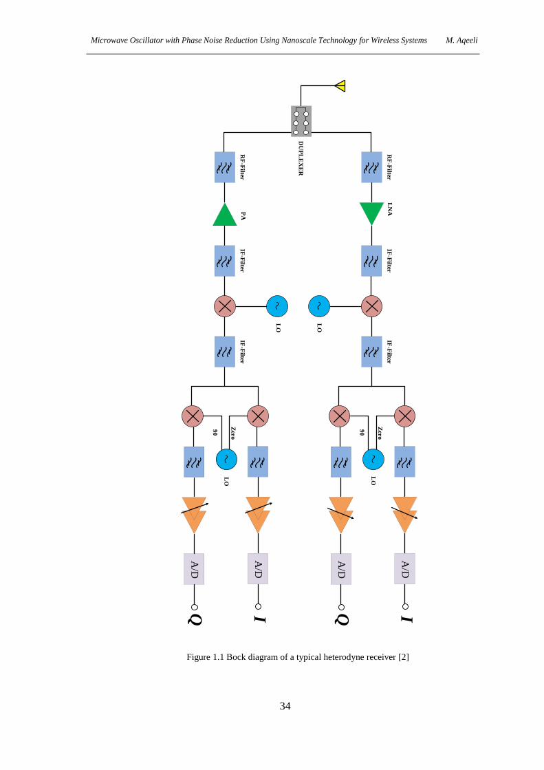
of the LO. A typical heterodyne receiver employed in wireless communication systems
is depicted in Figure 1.1. The incoming radio frequency (RF) signal from the antenna
is first filtered by a band select filter that removes the out-of-band signals. It is then
amplified by a low noise amplifier (LNA), which also suppresses the contribution of the
noise from the succeeding stages.
Microwave Oscillator with Phase Noise Reduction Using Nanoscale Technology for Wireless Systems M. Aqeeli
34
IF-F
ilter
A/D
I
A/D
Q
IF-F
ilter
RF
-Filte
rL
NA
Zero
90
IF-F
ilter
A/D
I
A/D
Q
IF-F
ilter
RF
-Filte
r
LO
PA
Zero
90
DU
PL
EX
ER
LO
LO
LO
Figure 1.1 Bock diagram of a typical heterodyne receiver [2]

Microwave Oscillator with Phase Noise Reduction Using Nanoscale Technology for Wireless Systems M. Aqeeli
35
The LNA output is then filtered by an image-reject filter to remove the image, which
has an offset of twice the intermediate frequency from the desired channel signal,
before being down-converted to the intermediate frequency (IF) by the mixer. A
channel-select filter then performs channel selection at the IF, and after that
demodulation or detection is carried out to retrieve the desired information. The
generated signal from the radio frequency local oscillator (RFLO) on the receiver side
is implemented to translate the incoming signal into a lower intermediate-frequency (IF)
range. Channel selection can be accomplished at the intermediate frequency local
oscillator (IFLO), depending on the layout architecture of the system. Solutions for
integrated systems usually use zero-IF radio architecture, which transforms the
incoming RF signal to a baseband frequency range accompanied by an LO. The zero-IF
radio architecture permits the full integration of RF front-end functionality by avoiding
the IF filter. The transmit up-conversion is carried out in a double conversion systematic
plan or arrangement. Furthermore, the IFLO and RF signal can be shared between the
transmitter and the receiver in time-division duplexing systems. The baseband signal
needs to be digitized using an analogue to digital (A/D) converters which provide
digitized receiver signal to be processed in a digital processing unit.
LOs and VCOs are the key factors in creating PLL frequency synthesisers employed to
generate a certain frequency. Figure 1.2 shows that each PLL employs a crystal
oscillator as a reference signal and VCO which synthesise output signal [1]. It is well
known that crystal oscillators are characterised by a very high-quality factor, a very
stable signal, low levels of phase noise and excellent performance and accuracy. The
disadvantages of crystal oscillators are their dependency on mechanical vibration for
resonant behaviour. As a result, they are large in size when compared to other surface-
Microwave Oscillator with Phase Noise Reduction Using Nanoscale Technology for Wireless Systems M. Aqeeli
36
mount technology (SMT) components. Furthermore, they cannot be synthesised to be
implemented as an LO or be designed in the RF frequency range. This research will
focus on the oscillator’s design implementing different technologies, more specifically
the LC-VCOs, which are key factors in the general frequency synthesiser block
diagram.
1.2: PLL fundamentals
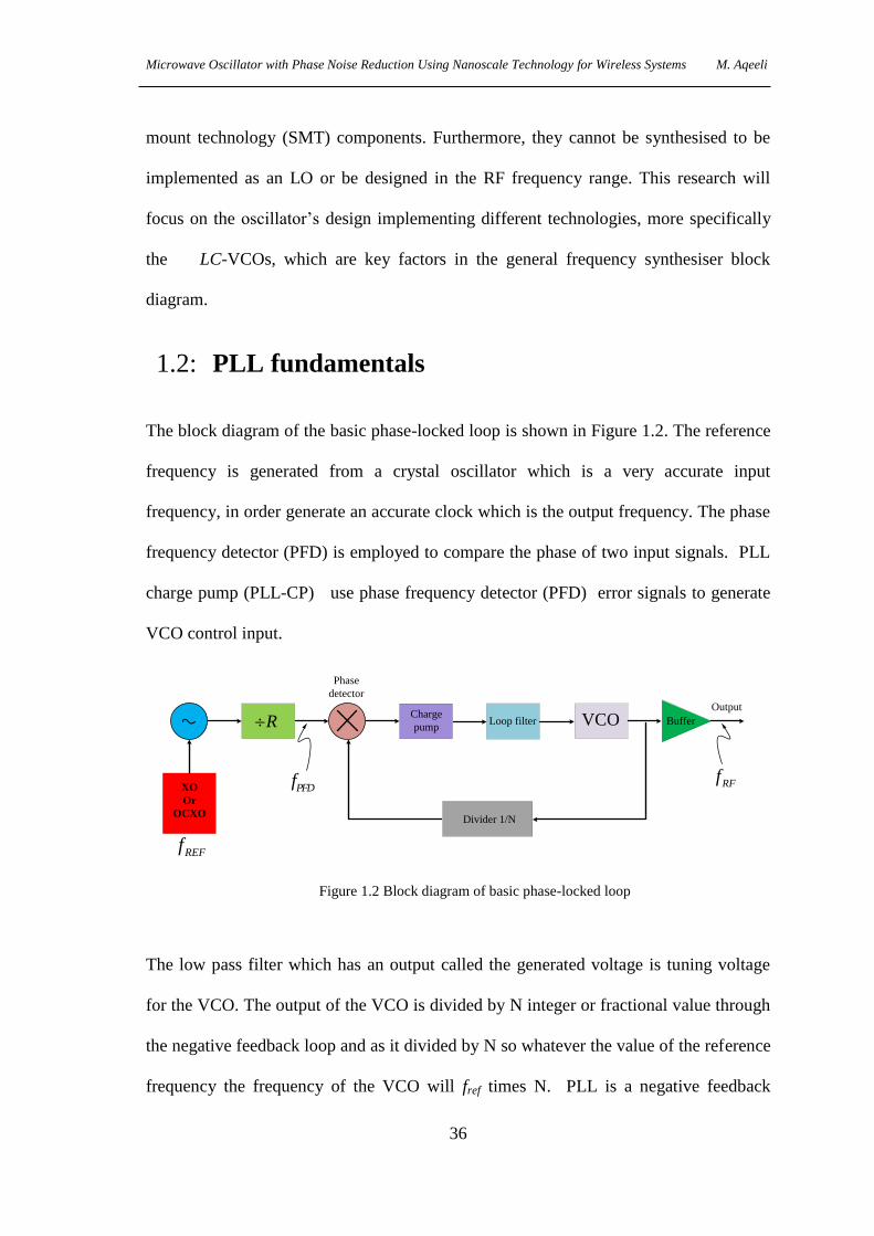
The block diagram of the basic phase-locked loop is shown in Figure 1.2. The reference
frequency is generated from a crystal oscillator which is a very accurate input
frequency, in order generate an accurate clock which is the output frequency. The phase
frequency detector (PFD) is employed to compare the phase of two input signals. PLL
charge pump (PLL-CP) use phase frequency detector (PFD) error signals to generate
VCO control input.
Phase
detector
Charge
pumpLoop filter VCO Buffer
Divider 1/N
Output
XO
Or
OCXO
RFf
REFf
PFDf
R
Figure 1.2 Block diagram of basic phase-locked loop
The low pass filter which has an output called the generated voltage is tuning voltage
for the VCO. The output of the VCO is divided by N integer or fractional value through
the negative feedback loop and as it divided by N so whatever the value of the reference
frequency the frequency of the VCO will fref times N. PLL is a negative feedback

Microwave Oscillator with Phase Noise Reduction Using Nanoscale Technology for Wireless Systems M. Aqeeli
37
system, as depicted in Figure 1.3, and it has the ability to multiply a reference signal,
where [1]. The performance of the PLL’s phase can be modelled mathematically, while
the characterisation of the PLL can be determined by implementing the control theory.
Phase
detectorLoop filter VCO
Divider 1/N
( )F sout
div
ref2
CPI
2 VCOK
s
PFD/CP
Figure 1.3 PLL linear model [1]
From the feedback system, the transfer function can be written as follows:
2( ) . ( ).
2
CP VCOI KG s F s
s
(1.1)
where 2CPI is PFD/CP gain, F(s) is the transfer function of the low pass filter and
2 VCOK is the gain of the VCO. With regard to third-order PLL, elements of the
passive loop filter are depicted in Figure 1.4.
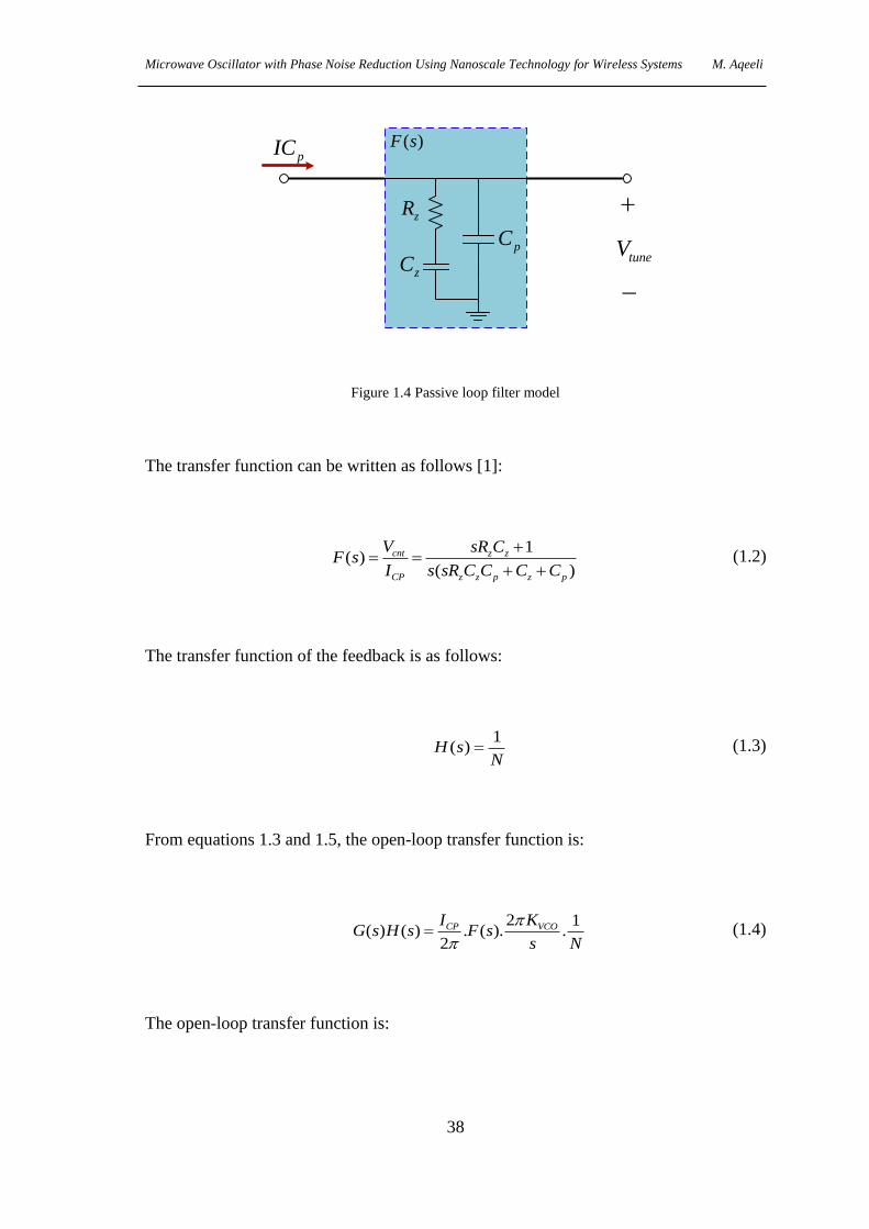
Microwave Oscillator with Phase Noise Reduction Using Nanoscale Technology for Wireless Systems M. Aqeeli
38
zR
zCpC
tuneV
( )F spIC
Figure 1.4 Passive loop filter model
The transfer function can be written as follows [1]:
1( )
( )
cnt z z
CP z z p z p
V sR CF s
I s sR C C C C
(1.2)
The transfer function of the feedback is as follows:
1
( )H sN
(1.3)
From equations 1.3 and 1.5, the open-loop transfer function is:
2 1( ) ( ) . ( ). .
2
CP VCOI KG s H s F s
s N
(1.4)
The open-loop transfer function is:

Microwave Oscillator with Phase Noise Reduction Using Nanoscale Technology for Wireless Systems M. Aqeeli
39
( ) ( )
( ) 1 ( ) ( )in
H s G s
s G s H s
(1.5)
In order to define the parameters of the loop filter, the open-loop frequency response,
( ) ( )s j
G s H s
, is implemented by ensuring loop steadiness. The open-loop frequency
response can possibly be written in terms of the loop parameters ICP, KVCO and the loop
filter time constants, which are as follows [1]:
.z p
p z
z p
C CR
C C
, (1.6)
z z zR C , (1.7)
2
1( ) ( ) .
( ) 1
CP VCO z
s jz p p
I K jG s H s
N C C j
(1.8)
Under the condition of known loop filter parameters, crossover frequency can be
defined as follows:
.CP VCO z zc
z p
I K R C
N C C
(1.9)
The phase margin for loop steadiness can be guaranteed when Z =1/Tz selects factor
below c and P =1/Tp selects a factor above c . If and is equal to four,
Microwave Oscillator with Phase Noise Reduction Using Nanoscale Technology for Wireless Systems M. Aqeeli
40
then a phase margin of 60o is achieved. From the loop parameters, the loop filter
components’ values are calculated as follows:
.z c
CP VCO
NR
I K (1.10)
2.CP VCO
z
c
I KC
N
(1.11)
2
1.CP VCO
p
c
I KC
N (1.12)
1.3: VCOs
Wireless communication applications require a tuneable oscillator, known as a VCO,
that can be built at RF frequencies when the output frequency of a device is a function
of a control input voltage, it nominated as VCO. Generally, there are two different kinds
of VCOs in most chips, the majority of which are based in LC tank VCOs, while the
other types are ring oscillators, which are simply a series of cascaded inverters used
when phase noise applications are not critical. In most applications, such as cellular
systems and WiFi, which requires strengthened phase noise performance, clean and
sophisticated oscillators are mandatory, which can be obtained through LC-VCOs. The
fundamental property of an LC-VCO is the LC tank, composed of an inductor and a
resistor. If energy is injected into this tank it will oscillate with a frequency of
oscillation fosc , which equates to:

Microwave Oscillator with Phase Noise Reduction Using Nanoscale Technology for Wireless Systems M. Aqeeli
41
1oscf
LC (1.13)
In reality, what happens is that on-chip inductors do have finite loss, the series
resistance Rs, which in turn is inversely proportional to the quality factor of the inductor
[1]. The nominated Q factor typically varies from 10-15 in 0.35µm CMOS technology.
Surprisingly, though, in modern nanoscale CMOS technology, this figure can be closer
to 20, and as the value of the Q factor increases, Rs decreases. It can be suggested
confidently that if energy is injected into the LC tank in the presence of these losses,
oscillation might take place. However, the wave might dampen exponentially, due to
these losses, because of the inability to sustain this oscillation, and it will eventually die
out. Consequently, in order to overcome the loss of the inductor, Rs can be replaced
initially by an equivalent resistor parallel to the LC tank, called Rp, which can be given
roughly as Rp ~ Q(L ), i.e. the lossy part, bearing in mind that this transformation is
only valid for narrowband frequencies when the Q factor is high. Nowadays, two parts
are available, namely the lossless part represented by the LC tank and the lossy part, so
in this instance if energy is injected into this system, it will not oscillate, because the
lossy part will kill any oscillation. Therefore, negative resistance, -R, is required to
cancel out Rp, because when energy is injected it starts oscillating and will keep on
oscillating. This is the basic principle of the oscillator for an LC tank which needs to
overcome losses, primarily due to the existence of the inductor.
An ideal VCO usually has output frequencies which function in line with its input
control voltage. The output of an ideal VCO can be represented as follows:

Microwave Oscillator with Phase Noise Reduction Using Nanoscale Technology for Wireless Systems M. Aqeeli
42
0out VCO tuneK V (1.14)
where 0 is the frequency at tuneV , equal to zero volts, and VCOK is the sensitivity or the
gain of the VCO in MHz/V. The obtainable tuning range, shown in Figure 1.5, is equal
to 2 1 .
Tuning voltage (V)
Fre
qu
ency
(GH
z)
0
2
1
,mintuneV ,maxtuneV
Figure 1.5 Desired operation regions for a VCO tuning curve.
Generally, VCOs exhibit very poor performance, and they are unstable due the lower
value relating to their Q factor of the resonator or the LC tank. A huge amount of effort
has been expended in designing VCOs, and for a long time they have remained a major
challenge to many researchers and manufacturers and thus have received the most
attention in recent years, as proved by the large number of publications in this field. In
order to evaluate the specifications and the performance of a VCO, important
components are available, for example oscillation frequency, phase noise, bandwidth
and power consumption. Phase noise plays an important role in these specifications.
Traditionally, a VCO has been implemented as a stand-alone module separate from

Microwave Oscillator with Phase Noise Reduction Using Nanoscale Technology for Wireless Systems M. Aqeeli
43
other PLL circuit blocks and then combined on the PCB board in a hybrid manner.
Moreover, it is usually encapsulated, using tinned iron to isolate it from external noise.
A VCO needs to be a separate module for several reasons. RF front-end low-noise
amplifiers (LNAs), circuits such as power amplifiers (PAs), mixers and switches have
been designed predominantly in III-V compound semiconductor technologies.
However, unlike other RF circuits, a Si BJT has been accepted generally as the best
candidate for an oscillator because of its low flicker noise and high gain characteristics.
Moreover, only an LC tank consisting of off-chip high-Q passive components enables
an oscillator to meet strict phase noise specifications for wireless handset applications.
Using Si BJTs and off-chip passive components forces it to be a separate module. Even
though wireless mobile technology has grown tremendously during the last 15 years,
customers continue to demand ever smaller and less expensive electronic wireless
products [3]. The most attractive approach to meet these growing requirements is a
silicon-based single-chip radio [4]. Developed technology in the area of Si-based
integrated circuits (ICs) permits a high level of integration but at an economic cost.
With the minimum feature size of CMOS approaching the nano-scale, and the
emergence of SiGe-wideband gap technology on Si substrates, an Si-based RF front-end
module has been considered as a possible solution because of its excellent active device
frequency characteristics [5]. Even though a Si-based single-chip radio has already
been proposed, it has suffered from several drawbacks that need to be overcome. One of
the most critical drawbacks of Si technology is the poor Q of the passive components;
this shortcoming results from the thin metallisation process and lossy Si substrate. Poor-
quality passive components, especially low-Q inductors, prevent the Si-based single-
chip radio from being the best solution.

Microwave Oscillator with Phase Noise Reduction Using Nanoscale Technology for Wireless Systems M. Aqeeli
44
As the peremptory requirement for high-performance, cheaper, smaller and more
advanced power-efficient wireless transceivers continues to increase, manufacturers put
a lot of effort into integrating as much as possible of the transceiver and the tracking
signal generator’s circuitry onto a single piece of silicon. On the other hand, it has been
very difficult to integrate high-tolerance inductors and high Q, though investigations
have established that the IC fabrication process is inexpensive. There could be many
types of LC-VCOs, but their numbers in practical use are rather limited, due mostly to
limitations in relation to bandwidth, significant phase noise variations and high power
consumption. The most critical parameter for any oscillator is phase noise, which is
widely used to characterise the performance and the spectral purity of both oscillators
and VCOs as well as frequency stability. For example, in receivers, the phase noise of
the LO restricts the ability and the sensitivity to detect a weak signal in the presence of a
strong signal, while transmitter phase noise results in energy being transmitted outside
of the required band [6]. Researchers always aim to lower phase noise, and in order to
assist in achieving this goal, a high quality factor or in the other words minimum loss
capacitors and inductors, is needed.
1.4: MOM capacitors
In general the required tuning range for VCOs is only a few percent. This is especially
true at the Gigahertz bandwidth since the application bandwidth is much smaller than
the centre frequency. If tuning is used to overcome the process variations a much larger
tuneability is required. A fully integrated VCO will typically exhibit a centre frequency
variations of +/-10%, this is mainly due to on chip capacitance variations. In order to
change the centre frequency to design a VCO, the LC-tank must be changed
Microwave Oscillator with Phase Noise Reduction Using Nanoscale Technology for Wireless Systems M. Aqeeli
45
electronically using digitally controlled switches. Typically, the wider the frequency
tuning range, the stronger the varactor’s tendency to convert AM into FM. The tuning
range of a MOS varactor develops with the difference between the minimum and
maximum small-signal capacitance Cmax-Cmin. This indicates that wide tuning range is
complemented with low phase noise. However, there is a big chance to decouple tuning
range from phase noise at the cost of a more complex control scheme. An array
consisting of fixed capacitors controlled digitally can tune the oscillator to the desired
set of discrete frequencies[7].
A varactor’s variable capacitance will cover the required gap not the full tuning range
but only between adjacent discrete frequencies. In the presence of some elements in the
switched capacitor array this gap minimized to smaller fragments of the full tuning
range. Most importantly is that only the varactor does convert AM into FM but not
fixed capacitors. In this method, the tuning range might be extended by adding fixed
capacitor arrays without degrading the sensitivity to AM–FM conversion.
MOM capacitors are widely used as fixed capacitors, due to their low cost, high
capacitance density, symmetrical plate design, superior RF characteristics, low parasitic
capacitance and no process steps or additional masks. MOM capacitors rely on coupling
capacitance which exist between metal fingers placed parallel to one another. In
symmetric-type MOM structures, the practical design made up of two ports, and the
number of fingers per layer is restricted to even numbers only, this is to ensure
symmetry. MOM capacitors take the advantage of the effect of intralayer capacitive
coupling between the plates formed by standard metallization wiring lines and vias.
Microwave Oscillator with Phase Noise Reduction Using Nanoscale Technology for Wireless Systems M. Aqeeli
46
Lateral capacitive coupling provides better matching characteristics than vertical
coupling due to a better process control of lateral dimensions than that of metal and
dielectric layer thicknesses. To increase the capacitance density, several metal layers are
connected in parallel by vias, forming a vertical metal wall or mesh. Normally, lowest
metal layers with minimum metal line width and spacing are used for MOMs to
maximize the capacitance density.
1.5: Literature review
Increases in both the complexity and size of VLSI circuits over the last several decades
need no reiteration. Microelectronics and its associated disciplines have undergone a
spurt in growth that cannot be matched by any area of science or engineering in the
history of technology. What is perhaps less obvious, though, are the ways in which
methods through which design methodologies and attitudes towards computer
assistance have been forced to adapt. VCOs have gained considerable attention in recent
years, mainly because of two reasons. The first is their importance in many applications
such as aerospace, point-to-point microwave backhaul calibration instruments and
defence, broadband and other commercial communications applications. The second
one involves rapid developments in CMOS process technology and metamaterial
technology.
A considerable amount of books have focused on the theory behind and the design and
implementation of oscillators and VCOs [1, 8-13]. In addition, a huge number of quality
papers have been published in support of a variety of oscillators and VCOs, leading to
some good solutions for many challenging parameters, such as wide tuning range, low
Microwave Oscillator with Phase Noise Reduction Using Nanoscale Technology for Wireless Systems M. Aqeeli
47
phase noise performance, highly linear tuning, stable performance at temperature
extremes, circuit architecture and low power consumption. Some of these designs
provide cutting-edge solutions for challenging communications requirements.
Designing an LC-VCO is a real challenge, even though CMOS technology has
developed rapidly. This is especially true mainly due to the characterisation of available
varactors. This literature review focuses on research and publications relating to centre
oscillation frequency ranges between 1 to 7.2 GHz as well as work related mainly to
fully integrated CMOS LC-VCOs featuring low phase noise, wide tuning ranges, low
power consumption and quality FoM.
A recently published, fully integrated CMOS LC-VCOs including all specifications and
key figures which feature sizes between 65nm and 0.35µm are considered as invaluable
for the interrogatory. Typical CMOS technology offers two modes of capacitor: the
inversion-mode MOS capacitor and the accumulation-mode MOS capacitor.
Accumulation-mode nMOS and Inversion-mode pMOS varactors can provide a
significant VCO tuning range, but quality factor (Q) variations near the threshold cause
VCO phase noise to fluctuate in relation to tuning voltage, as shown in Figure 1.6 In
some designs, in fact, phase noise variations exceed 20 dB. According to information
available to the authors, it seems that this problem is not as widely acknowledged in the
literature as perhaps it should be [14].

Microwave Oscillator with Phase Noise Reduction Using Nanoscale Technology for Wireless Systems M. Aqeeli
48
Figure 1.6 Phase noise of VCOs with accumulation-mode nMOS, inversion mode pMOS and varactor
diode.
VCO gain (KVCO) variation issues must be considered carefully when the tuning range
of a VCO becomes very wide. KVCO variation increases in line with the frequency tuning
range of the VCO, which in turn makes it more difficult to optimise the performance of
the PLL. In addition, using a MOS transistor as a varactor will increase the probability
of converting AM noise to FM noise. Therefore, switching capacitors are mandatory for
maintaining minimum phase noise, tuning linearity and low VCO sensitivity when the
tuning range is more than 30%. Studies using switching capacitors inside the LC tank
have been conducted, in order to extend the tuning range and to improve VCO phase
noise. These techniques are effective in widening frequency tuning, improving phase
noise performance and lowering KVCO. However, measured phase noise has been
relatively high, varying from -90.2 dBc/Hz 5 to -122 dBc/Hz.
4.8 5.0 5.2 5.4 5.6
-132
-128
-124
-120
-116
Ph
ase
no
ise
at
1M
Hz o
ffse
t(d
Bc/H
z)
Frequency of operation(GHz)
Accumulation-mode nMOS varactor
Inversion-mode pMOS varactor
Diode varactor

Microwave Oscillator with Phase Noise Reduction Using Nanoscale Technology for Wireless Systems M. Aqeeli
49
This work emphasises dramatic changes in phase noise over the tuning range. However,
recently published studies related to the phase noise performance of VCOs usually
obscure this problem and report simulating or measuring phase noise at a certain offset
frequency from the carrier frequency, only or at a small number of chosen tuning
voltages. When designing an oscillator or a VCO, it should be borne in mind that the
main concept of phase noise must centre on the characterisation of an oscillator or the
VCO, in order to maintain relatively exact phase noise performance over a specified
tuning range.
Phase noise is mandatory for many transmitting and receiving systems [15]. Transmitter
signal purity and adjacent channel rejection, for instance, are dependent on the phase
noise of a local oscillator. In a heterodyne system, when mixing an undesirable phase
noise (noisy) local oscillator with clean a low phase noise RF signal, a noisy IF signal
will be produced. When generating a high-frequency signal, low phase noise is
essential. Phase noise is the measure of variations and unwanted changes in the phase
of a signal. When implementing a PLL synthesiser in any communication system or
measurement instrument, overall phase noise consists of a synthesis of the different
components and circuit blocks that subscribe to the conclusive value. The phase noise
of oscillators is transferred to the carrier to which the receiver is tuned and is then
demodulated. Phase noise can be described in many methods, but the most common one
is the single sideband (SSB), which is denoted as L∆f. The United States of America’s
National Institute of Standards and Technology (NIST) defines L∆f as the ratio of the
power density at an offset frequency to the total power of the carrier signal with unit
dBc/Hz [16]. For simulation and measurement comparisons, generally, they normalise

Microwave Oscillator with Phase Noise Reduction Using Nanoscale Technology for Wireless Systems M. Aqeeli
50
to 1MHz frequency offset, assuming a 1/∆f2 characteristic of the skirt of the phase
noise as follows:
2
2 10log m
m
fL f L f
f
(1.15)
where mL f is the measured phase noise at a measured offset frequency mf in
dBc/Hz. The difficulty involved in comparing several VCOs was noted during this
study, as each design has different oscillation frequencies and different tuning ranges,
and they may also have different bias currents and supply voltages. Therefore, in order
to assess the performance of any oscillator or LC-VCO architecture, a widely accepted
and applied FoM was introduced in [16] to describe the performance features of a
system or a device. This FoM computes the reciprocal action of the phase noise of the
oscillator, the first-order oscillation frequency and power consumption [16]. The
implemented model to assess phase noise is as follows:
2
02 10log .
2sig
fkTL f
P Q f
(1.16)
where k is the Boltzmann constant, T is absolute temperature, Psig is the signal power of
the output, f0 is the oscillation frequency, Q is the quality factor of the oscillator tank
and ∆f is the frequency offset. The FoM can be defined as follows [16]:

Microwave Oscillator with Phase Noise Reduction Using Nanoscale Technology for Wireless Systems M. Aqeeli
51
2
0
sup
210log .
fkTPFN L f
P f
(1.17)
Note here that the better performance of the VCO, the higher the FoM. Although there
are many published works on different and specific VCO designs, they tend to focus on
the fundamentals, while topology studies are very rare. The exception to this rule,
presented in [17-19], reveals the design methodology for nMOS-pMOS cross-coupled
LC tank VCOs. This particular design, published in [19], focuses on an inductance
selection scheme, run through a method called an ‘insightful graphical’, to reduce phase
noise subject to different design obstacles imposed on tuning range, power
consumption, tank amplitude, oscillation start-up and the size of spiral inductors. A
method for optimising and specially automating components for CMOS LC oscillators
is presented in [17]. Phase noise characterisation in VCO design and implementation is
a fundamental issue, but it seems to be that the phase noise model presented by D. B.
Lesson [20] is the most qualitatively valid model. Recently, a new physical model has
been presented in [21-23]. The authors argue that the model has the ability to make
quantitative predictions regarding both jitter and phase noise for many kinds of
oscillators and VCOs.
1.6: Motivation and research objectives
Due to major advances and developments in the communication technology and
semiconductor fields, the world of wireless communication has developed rapidly in the
last two decades, from simple devices such as pagers to an emerging new generation of
cellular phones. PLL frequency synthesisers, which are critical components in
Microwave Oscillator with Phase Noise Reduction Using Nanoscale Technology for Wireless Systems M. Aqeeli
52
communication systems, have been the main topic of extensive research efforts in recent
years. The synthesiser works as a local oscillator for channel selection and frequency
translation in broadband cable tuners and wireless transceivers. In addition, it performs
as a clock synthesiser for data transforms in the analogue-digital signal interface. One of
the more difficult elements of PLL design is the VCO, which is covered in this thesis
from a design point of view as well as analysis and implementation. The specifications
of VCOs have gained considerable efforts in the research. Consequently, there have
been considerable advances in VCO and PLL design techniques and harmonious
developments in performance. Due to the importance of phase noise in VCO
performance, much of the research work mentioned above has focused on
correspondingly minimising this issue by employing different methods. As a result,
there has been some research on high-performance wideband VCOs and PLL
synthesisers. It seems to be none of the current published work clearly indicated the
problem of phase noise variation
This research focuses on both fundamental and advanced design techniques for ultra-
low phase noise and wideband VCOs. A cross-coupled differential VCO with low phase
noise variation is presented herein. The VCO’s core adopts a metal-oxide-metal (MOM)
digital switching capacitor array (DSCA), which is connected in series and in parallel to
the nMOS varactor, in order to reduce KVCO variation. For further gain linearity, a wider
tuning range and minor phase noise variations, this varactor bank is connected in
parallel to four nMOS varactor pairs. Each pair is biased at a different voltage. The
proposed VCO has been designed and implemented within UMC 130-nm, 6-metal
CMOS technology [14]. A new oscillator is presented with a novel microstrip low phase
noise oscillator based on a left-handed (LH) metamaterial bandpass filter which is

Microwave Oscillator with Phase Noise Reduction Using Nanoscale Technology for Wireless Systems M. Aqeeli
53
embedded into the feedback loop of the oscillator. The oscillator is designed at the
complex quality factor Qsc peak frequency, in order to achieve excellent phase noise
performance. A prototype is implemented to validate the research analysis and to
demonstrate the feasibility of the low phase noise oscillator. To the author’s best
knowledge, these solutions offer a reduction in phase noise and improve the
performance of microwave VCOs and oscillators.
The aims and objectives of this project include:
Design and simulate a high-performance 5.72 GHz VCO for the 130nm UMC.
MIXED MODE/RFCMOS processes. The design methodology must be
amendable for future technology and implemented using a range of software
tools.
Analyse and establish optimisation techniques for an oscillator based on LH
material at low cost and with low phase noise, high FoM, reduced size and easy
of fabrication.
Extends the potential of highly flexible and conductive graphene laminate to the
application of electromagnetic interference (EMI) shielding to offer the required
shielding from electromagnetic interference (EMI), not only for VCO phase
noise optimisation, but also for sensitive electronic devices.
Performance comparison with key existing technologies.

Microwave Oscillator with Phase Noise Reduction Using Nanoscale Technology for Wireless Systems M. Aqeeli
54
1.7: Problem statement
Phase noise performance is directly proportional to the gain of VCOs, and it is known
as KVCO. As a consequence, a large KVCO will amplify the noise coupling to the control
node and, as a consequence, degrade phase noise performance [24]. According to
information available to the authors, it seems that this problem is not as widely
acknowledged in the literature as it should be [25]. As indicated in section 1.2, the main
objective of this study is to present a novel varactor for VCOs design that can provide
low phase noise variation, wide tuning range, a competitive FoM, a compact size, low
power consumption and performance enhancements.
The design of wide tuning range VCOs is challenging, mainly due to the problem of
phase noise variations. In conventional microwave LC-VCOs, phase noise varies
dramatically over the tuning range of a VCO, but the published literature overshadows
this issue by measuring or simulating phase noise at the centre frequency. It is difficult
to obtain simultaneously a large tuning range and small phase noise variation, by
accommodating MOS varactors, because it increases the probability of converting AM
noise to FM noise [26]. This will grow in line with the difference between the
maximum and the minimum capacitances and may become indistinguishable from
phase noise. Thus, switching capacitors are vital to maintaining minimum phase noise
variations for wide tuning ranges and low VCO sensitivity, i.e. KVCO. Many research
works, which consider switching capacitors inside the LC tank, have been published, in
order to extend the tuning range and minimise VCO phase noise. However, these
studies have resulted in occupying a larger die area as well as exhibiting large phase
noise variations and higher power dissipation.

Microwave Oscillator with Phase Noise Reduction Using Nanoscale Technology for Wireless Systems M. Aqeeli
55
For low phase noise, it is necessary to have as small an amount of gain as possible, i.e.
KVCO. However, this smaller KVCO means a narrow frequency-locking range. Standard
CMOS technology offers diodes and MOS capacitors as varactors. In some designs
phase noise variations exceed 25dB. In a wide tuning range, variations between the
minimum and maximum values of the frequencies (fmax-fmin) will be large, thus meaning
large variations in KVCO [27]. In order to prove of this theory and to compare between
the studies presented in this thesis and other published works, a pMOS-only VCO
design, complete with body-bias varactors, was constructed and simulated. The result
shows clearly that the achieved tuning range reached oscillation frequencies ranging
from 4.4 to 5.4 GHz with phase noise variation of more than 16 dBc/Hz at a 1 MHz
offset. Therefore, there must be a solution to this conflict and a trade-off between the
frequency tuning range and KVCO variation.
High Q factor varactors that regularly have narrower tuning ranges and, as a result,
phase noise reduction at a certain frequency as well as phase noise variation, commonly
reveal undesirable manufacturing variations. Standard CMOS technology offers diodes
and MOS capacitors as varactors. nMOS in accumulation-mode and pMOS in
inversion-mode varactors can provide a significant VCO tuning range, while on the
other hand Q factor variations close to the Vth cause LC-VCO phase noise to fluctuate
dramatically in line with the control voltage. Phase noise variations vary dramatically
over the wide tuning range of VCOs.

Microwave Oscillator with Phase Noise Reduction Using Nanoscale Technology for Wireless Systems M. Aqeeli
56
1.8: Thesis organisation
The work in this thesis sets out to investigate, design, optimise, realise and characterise
wideband low phase noise variation and to gain linearised LC-VCO. The layout of the
thesis is detailed as follows.
Chapter One is a general introductory chapter. It first introduces an overview of
wireless communication and phase-locked loop (PLL) frequency synthesisers. It then
moves on to explain the implementation of oscillators and VCOs as a very important
and critical building block for almost every PLL frequency synthesiser or transceiver in
wireless communication, calibration and measurement instrument signal sources. It also
demonstrates how phase noise plays an important role in the specifications of
oscillators, VCOs and PLLs. In addition, it presents the challenges in and an overview
of the most recent research and publications in this area.
Chapter Two, any research work requires a strong foundation and in-depth background
study, so this chapter gives a general overview of the fundamentals of phase noise in
electrical oscillators, phase noise analysis, characterisation, design implications, phase
noise measurements and limitations of the presented mode and phase noise impact on
the overall efficiency and performance of the wireless system.
Chapter Three explains how VCOs are applied in modern multiband mobile radio
transceivers and then presents system design considerations and detailed parameters for
wideband VCOs. Also, it explains the problem of spectral purity in CMOS technology
and the contribution of AM-FM conversion noise. In addition, it explores the circuit
design considerations for wideband RF LC-VCOs and their implementation and

Microwave Oscillator with Phase Noise Reduction Using Nanoscale Technology for Wireless Systems M. Aqeeli
57
applications in fully integrated transceivers. In this section, switching discrete values of
capacitance or inductance from an LC tank, in order to design a wideband VCO, and its
trade-offs are discussed.
Chapter Four is mainly oriented toward dealing with those physical and device
modelling issues that constitute the foundations of the design of the proposed VCO. As
a part of this task, basic physics solid state principles are discussed. Following this, a
discussion on the influential characteristics of the materials used in the design of
microelectronics is presented. The design and simulation, as well as the steps in a
typical CMOS technology, will be considered, following which CMOS transistor
modelling will be analysed. In the last part of the chapter, a detailed study of noise
performance is presented.
Chapter Five, a particular study is introduced on a conventional type of varactor that
has been designed and implemented as a tuning device in the latest LC-VCO circuits.
Various types of varactor structures are implemented to describe the tuning curve of the
LC tank VCOs and their relationship with the C-V curve of varactors. Also, it explains
the requirements and the implementation of low-loss varactors in designing high-
performance LC oscillators and VCOs which require low-loss varactors, low phase
noise variation and a wide tuning range.
Chapter Six introduces the new approaches designed to conquer the problem of phase
noise variation, by using a metal-oxide-metal (MOM) digital switching capacitor array
(DSCA) which is added both in series and parallel to nMOS varactors. For further gain
linearising and minor phase noise variations, this chapter explains how a combination is
connected in parallel to four nMOS varactor pairs under inversion mode conditions.

Microwave Oscillator with Phase Noise Reduction Using Nanoscale Technology for Wireless Systems M. Aqeeli
58
Each pair is biased at different voltages to shift the tuning curves of varactors, while the
control signal for each group in the varactor bank is correlated to the control signal for
the binary weighted switched-capacitor bank. Such an approach enables the VCO to
produce an extended tuning bandwidth and minimises phase noise variations throughout
the entire tuning range while maintaining minimum die size. Furthermore, the chapter
demonstrates how previous resistors employed in recently published works have been
replaced with much smaller nMOS transistors, which perform as resistors, and then it
highlights the advantages of such approaches to gain linearisation, in order to provide a
significant improvement in VCO phase noise performance. Finally the practical design
and simulation results of the proposed VCOs, based on two new experimental VCO
circuit designs, are verified, thereby confirming the theory presented in the previous
chapters. The layout and measurement of two oscillators designed in this project, and
several phase noise improvement techniques, are summarised.
Chapter Seven, presents the practical design and simulation results of a novel
oscillator, based on miniaturised metamaterial bandpass filters with low phase noise, are
presented. In the proposed oscillator design, the passband filter is embedded into the
feedback loop, to be used as a frequency stabilisation element [74] The peak frequency
of the complex quality factor Qsc of the miniaturised filter is adopted in this project to
design the proposed oscillator as a substitution for implementing the group-delay-peak
frequency. To prove the effectiveness of the proposed concept, two filter-based
oscillators are designed and simulated using computer simulation technology (CST).
The first one was designed at the Qsc -peak frequency, while in the second one the
group-delay-peak frequency was used. It was found that the first oscillator achieved

Microwave Oscillator with Phase Noise Reduction Using Nanoscale Technology for Wireless Systems M. Aqeeli
59
excellent phase noise and was improved by more than 10 dB compared to the group-
delay-peak frequency oscillator – this improvement was experimentally verified.
Chapter Eight extends the potential of highly conductive graphene laminate to the
application of electromagnetic interference (EMI) shielding and proposes implementing
the achieved design to minimise the effects of continuous wave electromagnetic
interference (EMI) and to shield sensitive devices such as oscillators VCOs and PLLs.
Chapter Nine shows the details, identifies and discusses the key objectives achieved in
this work. A summary of the results and suggestions, and some directions for future
study, are also provided.
1.9: Main contributions
The general focus throughout this research is on the complete analysis of an oscillator
and VCO that is able to generate a wide range of RFs with low phase noise variations,
high FoM and low power consumption, and which is able to minimise a silicon area.
The initial discussion is on VCO phase noise variation and its impact on wireless
communication systems and calibration and measurement instruments. Prior to this
thesis, no mathematical analysis had demonstrated the gain of the VCO as a function of
the LC tank or the design parameters of the LC tank, which minimise the gain KVCO and
phase noise variation implementing a metal-oxide-metal (MOM) digital switching
capacitor array (DSCA) that is connected in series and in parallel to the nMOS varactor.
Without such analysis, it is impossible to draw any conclusions on a practical VCO
design. Therefore, it is essential to develop a novel oscillator and VCO with outstanding
specifications. First, this report focuses on oscillation criteria, namely in relation to

Microwave Oscillator with Phase Noise Reduction Using Nanoscale Technology for Wireless Systems M. Aqeeli
60
sensitivity to various circuit parameters. Second, as the oscillator is a large signal
device, the report covers the important topic of noise performance. The mathematical
description of the oscillator circuit is then concluded by introducing a new phase FoM.
All of these theoretical insights are proven through the design and simulation of a
practical LC VCO implemented in a CMOS circuit. The design procedure is presented
in a clear manner, and the reader can use it as a reference in the design of any VCO. The
proposed VCO circuit can be used as a new, fast, fully integrated VCO and as an
attractive alternative to the existing built-in examples. This work, introduce a novel
approach to gaining linearisation, in order to provide a significant improvement in VCO
phase noise performance. This approach is implemented by using a digitally switched
varactor bank (DSVB) together with a new 4-bit metal-oxide-metal (MOM) digital
capacitor switching array (MOMDCSA), which delivers reduced VCO tuning gain
along with low phase noise variation. Using this novel approach, it will be able to
optimise the VCO for phase noise and extend and linearise the tuning range. In order to
reduce VCO phase noise variation, a varactor bank is used, and each pair in the bank is
biased differently, to extend the range. Thus, VCO tuning gain reduces, and optimal
phase noise is obtained across a wide range of frequencies, accompanied by minimum
phase noise. When compared to recently reported work, the proposed VCO’s bandwidth
is increased by more than 10% and phase noise reduction by more than 10 dBc/Hz,
while phase noise variation is simulated at less than 4.9 dBc/Hz. In addition, based on
the analysis of a complex quality factor Qsc for an LH narrowband metamaterial filter, a
novel free-running oscillator has been designed to meet the most stringent phase noise
requirements in the L-band. It can conclude that the reported oscillator has better
performance, low cost and significant phase noise reduction than those published works
to date. A highly conductive graphene laminate printed on paper with the highly

Microwave Oscillator with Phase Noise Reduction Using Nanoscale Technology for Wireless Systems M. Aqeeli
61
advantages of being lightweight, flexible and low in cost. The advantages made
graphene laminate very promising in EMI shielding for electronics and wireless
communication devices.
1.10: Chapter summary
An overview of oscillators in wireless radio transceiver is introduced. The LO signal
quality has a huge impact on the radio transceiver performance. All parameters of
VCOs are described in detail. The PLL loop filter design and PLL frequency synthesis
are discussed. Phase noise problem is specified and the MOM capacitors are
overviewed. The thesis contribution and organisation are described.

Microwave Oscillator with Phase Noise Reduction Using Nanoscale Technology for Wireless Systems M. Aqeeli
62
Fundamentals of Chapter 2:
Phase Noise in Electrical
Oscillators
2.1: Introduction
A perfect oscillator would be able to produce a pure signal which could be represented
as a single spectral line. In the real world, sources have unwanted amplitude or consist
of small, random perturbations in the phase of the signal [28]. These phase-modulated
components are classed as ‘phase noise’. An ideal oscillator is a device that generates a
periodic signal with wanted properties. It would be characterised as a sine wave in the
time domain:
v(t) = A cos(2πf0t) (2.1)
Microwave Oscillator with Phase Noise Reduction Using Nanoscale Technology for Wireless Systems M. Aqeeli
63
where A is the amplitude and f0 is the frequency. However, in reality, a random
amplitude and phase noise are added to this signal, and so the instantaneous output of a
practical oscillator can be represented as follows:
v(t) = (A+a(t)) cos(2πf0t + φ(t)) (2.2)
where a(t) and φ(t) are the random amplitude and phase noise, respectively. Oscillators
do experience alterations in amplitude and in phase noise. Such alterations are caused
by both the internal noise generated by passive and active devices and by external
interference coupled with a power supply or a substrate.
Two different types of phase expressions arise as a result of oscillator output. The first
example appears as a prominent component in the spectrum‚ usually pointed out as a
spurious tone, while the second type of phase expression exists as random phase
alterations‚ noted as phase noise. Phase noise in oscillators is a very critical subject and
mainly appears because of internal noise sources, such as from active devices (flicker
noise or 1/f‚ shot noise) and thermal noise sources [29]. They can be described as being
random phenomena in nature. Spurious tones are caused by external noise sources, such
as tuning voltage noise‚ bias current sources, power supplies and required clock signals.
All of these parameters can be determined practically. With regard to the spurious tones,
it can be said that they are not directly related to oscillators, although they are very
important and sophisticated requirements in the output of frequency synthesiser
equipment and in PLL design specification parameters [30]. Amplitude noise is usually
less important in comparison with phase noise for oscillators, since it is suppressed by
the intrinsic non-linear nature of oscillators. Hence, amplitude fluctuations will die
away after a period of time in an oscillator. On the other hand, phase noise will

Microwave Oscillator with Phase Noise Reduction Using Nanoscale Technology for Wireless Systems M. Aqeeli
64
accumulate, resulting in the severe performance degradation of the electronic
instrumentation system in which the oscillator is used. Therefore, electronic
instrumentation wireless communication systems usually impose strict specifications on
the phase noise performance parameters of voltages controlling the performance of
oscillator noise, described as phase noise in the frequency domain and as jitter in the
time domain [31]. The importance of each element depends on the application;
therefore, calibration and measurement specialists, as well as microwave engineers, care
about phase noise, whereas for digital signal processing specialists, jitter is important.
Generally, noisy oscillators are associated with phase noise and jitter. Therefore, as
phase noise increases in the oscillator, jitter will increase as well. In analogue designs,
phase noise is commonly described in the frequency domain [32]. The phase noise unit
is dBc/Hz, demonstrating noise power proportional to the carrier implicated in a 1 Hz
bandwidth at a certain frequency offset from the carrier. In ideal cases, oscillators
operate at the spectrum, whilst in realistic oscillators, the spectrum displays ‘skirts’
around the centre or ‘carrier’ frequency.
f0 f f0 2f0 3f0
Harmonics
Random phase
Spurious
signal
Figure 2.1 An ideal signal (left) and an actual signal with additional phase noise (right) [30]
There are two types of irregular rise and fall phase terms. The first expression,
characterised by discrete signals, is referred to as ‘spurious’ and appears as a form of
prominent synthesis in spectral density (see Figure 2.1). The second term, which is

Microwave Oscillator with Phase Noise Reduction Using Nanoscale Technology for Wireless Systems M. Aqeeli
65
classified as ‘random’ in reality, appears as a random phase alteration and is generally
associated with phase noise.
2.2: Phase noise specifications
In local oscillators and VCOs, signal phase noise plays a major role in the overall
efficiency and performance of the wireless system. This is done usually through
specifying how channels can be allocated in narrowband systems and how closely group
points are allocated in the I/Q plane in the form of digital modulated systems. The first
aspect determines phase noise power levels with regard to the carrier at a specific offset
frequency (dBc/Hz). This particular specification is normally imperative in cellular
systems which can be identified as narrowband systems [31].
To understand the importance of phase noise, consider a local oscillator (LO) which
provides the carrier signal to a mixer located in a frequency synthesiser system. When
the output of any local oscillators includes phase noise, then this phase noise will affect
both the down-converted and up-converted signals, and the required signal may be
accompanied by interference in an adjacent channel. Moreover, if two signals are mixed
with the output of the LO, then the down-converted band will consist of two
overlapping spectra, with the targeted signal encountering considerable noise resulting
from the tail of the interferer. This influence is defined as ‘reciprocal mixing’. Phase
noise on LO signals used for up- and down-conversion leads to the imperfect rejection
of nearby signals.

Microwave Oscillator with Phase Noise Reduction Using Nanoscale Technology for Wireless Systems M. Aqeeli
66
If the generated signal from local oscillators is noisy, this will definitely degrade the
performance of these systems. In locally transmitted signal applications, noises which
are close to the channel offsets will stop the clean reception of a remote signal in the
closed channel. On the other hand, noise on receiver LOs – at offsets equating to the IF
frequency – may affect the total capability and performance of the receivers. An
oscillator’s phase noise is used the single-sideband (SSB) phase noise ‚ which is
determined as the ratio of noise power in a 1 Hz bandwidth at an offset‚ fm, to the signal
power. SSB phase noise is determined in dBc/Hz at a certain frequency offset from the
carrier, fm [1].
( )( ) 10log noise m
m
signal
P fL f
P
(2.3)
Equation 2.3 can be written as follows:
,
2
2
,
( )( ) 10log n rms m
m
c rmssignal
V fL f
V
(2.4)
where ,
2 ( )n rms mV f is the rms value which represents the phase noise sideband at the offset
frequency 𝑓𝑚 from the carrier frequency, and 2
,c rmssignalV is the rms value of the carrier
signal. This SSB power can be caused by alterations in the amplitude or the phase of the
source. Sidebands near to the carrier derive either from the AM or PM modulation of
the carrier signal by noise, as shown in Figure 2.2.

Microwave Oscillator with Phase Noise Reduction Using Nanoscale Technology for Wireless Systems M. Aqeeli
67
fm
1 Hz
L( fm )
f0
Power
Spectrum PSignal
PNoise
f (Hz)
Figure 2.2 Phase noise definition [1]
Phase noise can be written with the contributions of AM and PM noise as follows [1]:
( ) ( )( ) 10log
2 2
m a mm
S f S fL f
(2.5)
where ( )mS f is double-sideband phase noise spectral density and ( )a mS f is double-
sideband amplitude noise spectral density. Assuming a signal of a fixed amplitude, and
that this signal is phase-modulated by a sine wave of frequency 𝑓𝑚, this signal can be
represented as [1]:
( ) ( sin )VCO c c p mS t A cos t t (2.6)
where Ac is a constant amplitude of a signal‚ c is the frequency of the signal, m is the
modulation frequency, p is peak phase deviation. If 2p then the narrowband
FM is used to obtain the following:

Microwave Oscillator with Phase Noise Reduction Using Nanoscale Technology for Wireless Systems M. Aqeeli
68
( ) ( ) cos( ) cos( )2 2
p p
VCO c c c m c mS t A cos t t t
(2.7)
The amplitude of the side band‚ 𝐴𝑠𝑝, as a result of the modulating signal, is written as
[1]:
2
c p
sp
AA
(2.8)
From Equation (2.8)‚ peak phase deviation‚ with amplitude 𝐴𝑠𝑝, around the carrier is
written as:
2p
c
Asp
A (2.9)
Supposing that the sidebands are caused by phase noise alterations‚ then the phase noise
power spectral density in Equations 2.4 and 2.9 can be expressed as [1]:
22
,
,
( ) ( )( )
2 2
m n rms mrms m
c rms
S f V ff
V
(2.10)
It should be noted that equation 2.10 represents the fundamental importance of
simulating and calculating phase noise in PLLs. Phase noise equations are helpful in
measuring and characterising using measurement tools‚ while the 𝜙( 𝑓𝑚) is
advantageous in calculating integrated residual phase deviation through the required

Microwave Oscillator with Phase Noise Reduction Using Nanoscale Technology for Wireless Systems M. Aqeeli
69
bandwidth. If the impact of the AM modulation of a carrier signal is included, the AM
modulated signal is expressed as [1]:
( ) (1 )cosVCO c m cS t A mcos t t (2.11)
Equation 2.12 can be expanded as:
( ) ( ) cos( ) cos( )2 2
VCO c c c m c m
m mS t A cos t t t (2.12)
As noted, equation 2.12 signifies that AM modulation produces a couple of spurious
sidebands which are identical to those seen in PM modulation, with the only variation
between the AM and PM sidebands being the phase link, as indicated in Figure 2.3. If
𝐿( 𝑓𝑚) is measured using a spectrum analyser‚ the AM and PM sidebands cannot be
distinguished, since spectrum analysers do not possess phase information. PM-
modulated noise dominates close to the carrier‚ and it might be accounted for as phase
noise. Both AM and PM noise contribute equally in far offset frequencies [1].
fc fC+ fm
fC - fm
PM
fc fC+ fmfC - fm
AM
(a) (b)
Figure 2.3 Sidebands around the carrier as a result of AM (a) and PM (b) [1]

Microwave Oscillator with Phase Noise Reduction Using Nanoscale Technology for Wireless Systems M. Aqeeli
70
2.3: Characteristics of oscillator noise
Oscillator phase noise has a very significant effect on the all of the noise attributes of a
PLL. Every PLL regularly utilises two oscillators, namely an RF VCO and a reference
crystal oscillator. Phase noise in oscillators has an effect on the close-in phase noise of a
PLL, while VCO noise overcomes and formulates the noise of the PLL. An oscillator’s
noise exhibits various slopes in different regions. Figure 2.4 shows phase noise versus
log frequency in decibels. These plotted regions have slopes of 0‚1/f, 1/f 2 and 1/f
3. The
noise plot of a MOSFET or Bipolar transistor indicates that they have only two regions,
namely thermal noise and the 1/f region, as shown in Figure 2.5. The noise of the
active and passive devices is driven into the resonators of oscillators and VCOs, and it
will affect every system, especially those used in communications. This noise will be
shaped on each side of the oscillation frequency by the VCO resonator, and as a
consequence thermal noise becomes 1/f 2 and noise becomes 1/f
3 along the resonator’s
bandwidth [1]. The particular characteristics of RF LC tank oscillators are shown in
Figure 2.4(a), while Figure 2.4(b) models the characteristics of a high-Q crystal
oscillator.
1𝑓𝑚
2
1𝑓𝑚
3
𝑓0
2𝑄
𝑓1 𝑓
fm
L ( fm)
1𝑓𝑚
1𝑓𝑚
3
𝑓1 𝑓 𝑓0
2𝑄
fm
L ( fm)
(a) (b)
Figure 2.4 VCO phase noise characteristics: (a) Low-Q (b) High-Q [1]

Microwave Oscillator with Phase Noise Reduction Using Nanoscale Technology for Wireless Systems M. Aqeeli
71
𝑓1 𝑓
20𝑙𝑜𝑔𝑉𝑛2
1𝑓𝑚
fm
L ( fm)
Thermal noise
flicker noise
Figure 2.5 Noise attributes of a MOSFET transistor in a fixed bias condition [1]
2.4: Quality factor and noise in LC VCO
The quality factor, Q, of the oscillator tank circuit is a very important design parameter
in determining oscillator performance. It is a critical issue that arises in oscillators, and
it can be stated confidently that the phase noise of an LC oscillator relies on the quality
factor of the LC tank circuit.
2.4.1: Quality factor
Oscillator phase noise is effected by the Q factor of an LC tank, where Q represents
energy lost as it is moved from the inductor to the capacitor, and vice versa. Therefore,
it is a primary objective of any oscillator research to obtain a high Q value. Three
definitions and interpretations of Q will be presented herein[33]. Firstly, Q is generally
defined as:
Energy stored
2 /Energy dissipated
Q cycle (2.13)

Microwave Oscillator with Phase Noise Reduction Using Nanoscale Technology for Wireless Systems M. Aqeeli
72
Secondly, Q can also be defined with respect to the phase of the open-loop transfer
function, Q at the resonance of the LC tank in an oscillator, as energy dissipated:
0
2
dQQ
d
(2.14)
where ωo is the resonant frequency. The quality factor of the system is a function of
phase deviation with respect to a change in frequency. Finally, Q can also be defined as
the ‘sharpness’ of the magnitude of the frequency response. Figure 2.6 illustrates the
one-port transfer response of a simple parallel RLC tank. Q can be calculated as
follows:
0
2 1
Q
(2.15)
Therefore, designing a tank circuit for minimal loss reduces its bandwidth, which results
in a signal that does not spill over as much into adjacent channels. Q can be defined
with respect to the phase ∅(𝑗𝜔) of the open-loop transfer function.
RPL1 C1( )X j ( )Y j
Figure 2.6 The open-loop transfer function

Microwave Oscillator with Phase Noise Reduction Using Nanoscale Technology for Wireless Systems M. Aqeeli
73
The transfer function of the circuit is equal to:
( )
( )( )
Y jH j
X j
(2.16)
The open-loop transfer function of the system= ( ) ( )H j Z j :
1 Im ( ( ))( ) tan
Re ( ( ))
ag Z jj
al Z j
(2.17)
The impedance that can be seen by the source is given by the following equation:
1 1 1
p
j CZ j L R
(2.18)
1
1 1
p
Z
j Cj L R
(2.19)
1 1 1 2
1
( ) tan tan ( ) (1 )1 p
p
CLj R L LC
R
(2.20)
Using 1
2
(tan ) 1
1
d u du
dx u dx
(2.21)
then:
2
2
1
1 (1 )p
d
d RLC
L
(2.22)

Microwave Oscillator with Phase Noise Reduction Using Nanoscale Technology for Wireless Systems M. Aqeeli
74
0
1
LC (2.23)
2
01 0LC (2.24)
0
2 p
dCR
d
(2.25)
The equivalent expressions for the circuit Q factor are given by:
0
00
2
p
p
C
RdQQ CR
d X
(2.26)
0
1CX
C (2.25)
at resonance XC=XL , where 0LX L
0
00
2
p
p
C
RdQQ CR
d X
(2.27)
For steady state oscillation, total phase shift around the feedback loop must be zero. If
the oscillator frequency deviates slightly, due to noise injection, then the larger the
change in the loop phase, the greater the tendency for the oscillator to return to its centre
frequency [12]. The open-loop Q is a measure of the level of the closed-loop system
resists variations in the frequency.
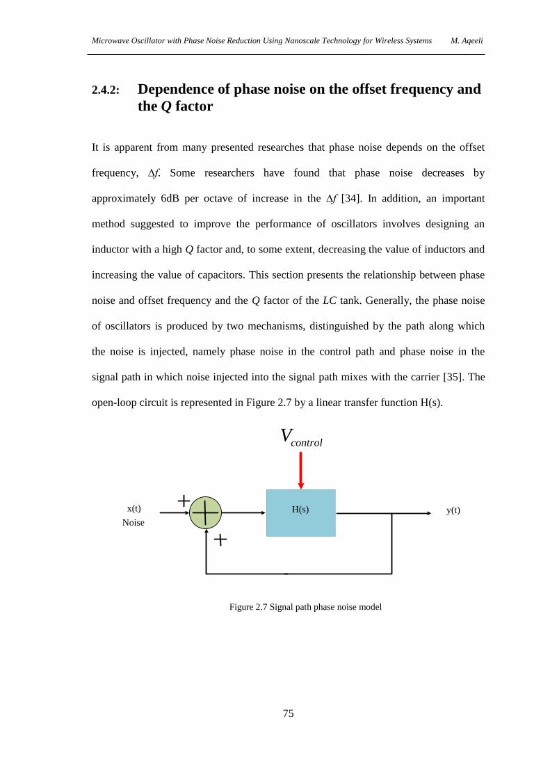
Microwave Oscillator with Phase Noise Reduction Using Nanoscale Technology for Wireless Systems M. Aqeeli
75
2.4.2: Dependence of phase noise on the offset frequency and
the Q factor
It is apparent from many presented researches that phase noise depends on the offset
frequency, ∆f. Some researchers have found that phase noise decreases by
approximately 6dB per octave of increase in the ∆f [34]. In addition, an important
method suggested to improve the performance of oscillators involves designing an
inductor with a high Q factor and, to some extent, decreasing the value of inductors and
increasing the value of capacitors. This section presents the relationship between phase
noise and offset frequency and the Q factor of the LC tank. Generally, the phase noise
of oscillators is produced by two mechanisms, distinguished by the path along which
the noise is injected, namely phase noise in the control path and phase noise in the
signal path in which noise injected into the signal path mixes with the carrier [35]. The
open-loop circuit is represented in Figure 2.7 by a linear transfer function H(s).
Noise
H(s) y(t)x(t)
controlV
Figure 2.7 Signal path phase noise model
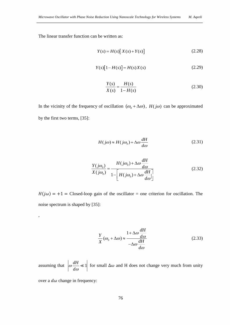
Microwave Oscillator with Phase Noise Reduction Using Nanoscale Technology for Wireless Systems M. Aqeeli
76
The linear transfer function can be written as:
( ) ( ) ( ) ( )Y s H s X s Y s (2.28)
( ) 1 ( ) ( ) ( )Y s H s H s X s (2.29)
( ) ( )
( ) 1 ( )
Y s H s
X s H s
(2.30)
In the vicinity of the frequency of oscillation 0( ) , ( )H j can be approximated
by the first two terms, [35]:
0( ) ( )dH
H j H jd
(2.31)
0
0
00
( )( )
( )1 ( )
dHH j
Y j ddHX j
H jd
(2.32)
𝐻(𝑗𝜔) = +1 = Closed-loop gain of the oscillator = one criterion for oscillation. The
noise spectrum is shaped by [35]:
,
0
1
( )
dH
Y ddHX
d
(2.33)
assuming that 1dH
d
for small ∆𝜔 and H does not change very much from unity
over a 𝑑𝜔 change in frequency:

Microwave Oscillator with Phase Noise Reduction Using Nanoscale Technology for Wireless Systems M. Aqeeli
77
0
1( )
Y
dHX
d
(2.34)
2
0 22
1( )
Y
X dH
d
(2.35)
= the factor by which noise introduced into the signal path is multiplied when it
appears at the output of the oscillator [35]:
j jd HdH dH
e j H ed d d
(2.36)
22 22d HdH dH
Hd d d
(2.37)
For an LC oscillator
2 22dH d
Hd d
(2.38)
since the Q is relatively high, H is close to unity and d H
d is not large enough for
oscillation to be sustained, since |𝐻| must remain close to unity [35]:
22
2
0
2dHQ
d
(2.39)
22
0
2
1( )
4
Yj
X Q
(2.40)
Therefore, the phase noise of an oscillator is proportional to 2
1
Q and
2
1
.

Microwave Oscillator with Phase Noise Reduction Using Nanoscale Technology for Wireless Systems M. Aqeeli
78
2.5: Phase noise in OFDM wireless systems
Phase noise is an important parameter when designing any communication system and
must be dealt with it very carefully. When phase noise existed, it might at the receiver
minimize the effective signal-to-noise ratio, and as a result, limit the bit error rate and
data rate. Phase noise arises mainly caused by the undesirable features or specifications
of the local oscillator (LO). Basically, for LOs it exemplifies a time-varying drift of the
phase from its reference. Phase noise effects in orthogonal frequency division
multiplexing (OFDM). It definitely causes significant degradation in the performance
the OFDM which is recognized modulation method for high data rate communications
over wireless links. Due to the fact that OFDM has the capability to eliminate inter-
symbol and capture multipath energy interference, therefore it has been selected as the
transmission method for many standards, including the IEEE 802.11g WLAN standard
in the 2.4-GHz band, the IEEE 802.11a wireless local area network (WLAN) standard
in the 5-GHz band, and the European digital video broadcasting system (DVB-T). in
addition to that, the OFDM-based physical layer is being paid attention by several
standardization groups, for instant, the IEEE 802.20 mobile broad- band wireless access
(MBWA) groups and IEEE 802.15.3 wireless personal area network (WPAN) and. The
raised up interest in OFDM has resulted recently in huge research in this field in order
making the real systems less costly in practice and most important more reliable. The
critical limitation of OFDM applications is that they are very sensitive to the phase
noise generated by local oscillators. The effect of phase noise on OFDM receivers has
been investigated in many published works discussed in [36]. The distortion issued by
phase noise is characterized by what is known as phase error (CPE) term and an inter-

Microwave Oscillator with Phase Noise Reduction Using Nanoscale Technology for Wireless Systems M. Aqeeli
79
carrier interference (ICI) term. The ICI term may be represented as additive Gaussian
noise while the CPE term accounts for the rotation of the constellation points in the
complex plane. OFDM transmits data symbols over many low-rate subcarriers. This
makes it more difficult to track and compensate for phase noise when compared to
single-carrier modulation methods.
As OFDM receivers are particularly sensitive to phase noise, strict constraints result in
the design and fabrication of oscillators and the associated circuitry, so that the
generated phase noise level is within the allowed limits of the system [36]. There are
many examples in literature which describe approaches to decrease the impact of phase
noise in digital systems. This approach provides a reliable, low cost solution to
overcome the problem of phase noise, whilst maintaining efficiency of the system.
Various works describe methods which compensate for the CPE term, where the
constellation rotation is estimated using pilot tones embedded in OFDM symbols before
the demodulator applies the correction [36]. The ICI effect is ignored or treated as
additive noise in these schemes. This means that if the phase noise varies quickly in
comparison to the OFDM symbol rate they will perform poorly.
There are essentially two types of oscillators. The most commonly used ones are free-
running oscillators operated without the PLL. In this scenario, the generated phase
noise is modeled as the accumulation of many unknown frequency deviations. In a PLL
oscillator, any variations in the phase of the carrier signal are tracked by the closed-loop
control mechanism. Thus, the generated phase noise will include a finite variance [37].

Microwave Oscillator with Phase Noise Reduction Using Nanoscale Technology for Wireless Systems M. Aqeeli
80
2.5.1: Free-Running Oscillator
For oscillators, the frequency deviation µ(t) is modeled as a zero-mean white Gaussian
random process with single-sided PSD N0=v/π , where v is the oscillator linewidth. The
phase noise ϕfree-osc(t) from a free-running oscillator is modeled by integrating µ(t), i.e.,
0( ) 2 ( )
t
free osc t d (2.41)
The single sided (PSD) of ( )free osc t is,
, 2( )free osc
vS f
f
(2.42)
For 0f . The carrier noise is ( )( ) j free t
free oscC t e
and its mean value satisfies
( ) 0free oscE C t (2.43)
As t . The autocorrelation function of ( )free oscC tis given by
( )free oscCR e
(2.44)
and the single-sided PSD of ( )free osc
C t
is Lorezian
, 2 2
4( )
(4 )free oscC
vS f
f v
(2.45)

Microwave Oscillator with Phase Noise Reduction Using Nanoscale Technology for Wireless Systems M. Aqeeli
81
Oscillator With PLLs 2.5.1.1:
The block diagram of a PLL system is depicted in Figure 2.8 [36]. The existing phase
error ϕ(t) between the carrier signal and the local oscillator is filtered through the low
pass filter which is represented by KdF(s). The resulting signal Vc is used as the input to
the oscillator so that its output will track the variations of the phase of the carrier signal.
The closed loop transfer function between the carrier phase signal θi and the oscillator
phase signal θo is given as follows
/
/
( ) ( )( )
( ) ( )
o p o d
i p o d
s K K F sH s
s s K K F s
(2.46)
Where o dK K is the open loop gain. Thus, the transfer function between the input phase
signal θi/p and the phase noise ϕ is
/ /
/ /
( ) ( )( )( ) 1 ( )
( ) ( ) ( )
i p o p
i p i p o d
s ss sG s H s
s s s K K F s
(2.47)
Loop Filter
Control Signal
×
Oscillator
Carrier Phase signal
0K
s
( )dK F s
Oscillator Phase signal
( )( )C d i oV K F s
i o Error Signali ×
oo C
KV
s
Figure 2.8 Block diagram of a PLL system [36]

Microwave Oscillator with Phase Noise Reduction Using Nanoscale Technology for Wireless Systems M. Aqeeli
82
Several loop filters will generate phase noise with several PSDs. Models for the first
order and second order PLLs that are widely used will be explained.
First order PLL: 2.5.1.2:
In this model F(s)=1 and the closed loop transfer function is given by:
( ) L
L
H ss
(2.48)
Where L o dK K is the angular frequency of zero decibel loop gain. Due to the fact
that input phase signal is produced by a free running oscillator, it is possible to let
/ ( ) ( )i p free osct t . After the PLL correction, the single sided PSD of the phase noise
( )APLL t can be represnted as follows[36]
2 2
, 2 2 2( ) ( 2 ) ( ) 1 ( 2 )
2 ( )A free oscPLL
L
v vS f G j f S f H j f
f f f
(2.49)
Where / 2L Lf is a measure of the loop bandwidth. The variance of ( )PLLA t is
given by
2
,
0
( )2PLL AA
PLL
L
vS f df
f
(2.50)
The autocorrelation function of ( )PLLA t can be calculated as follows
2
, 2 2( )
2 ( )A
j f
PLL
L
vR e df
f f
* (2.51)
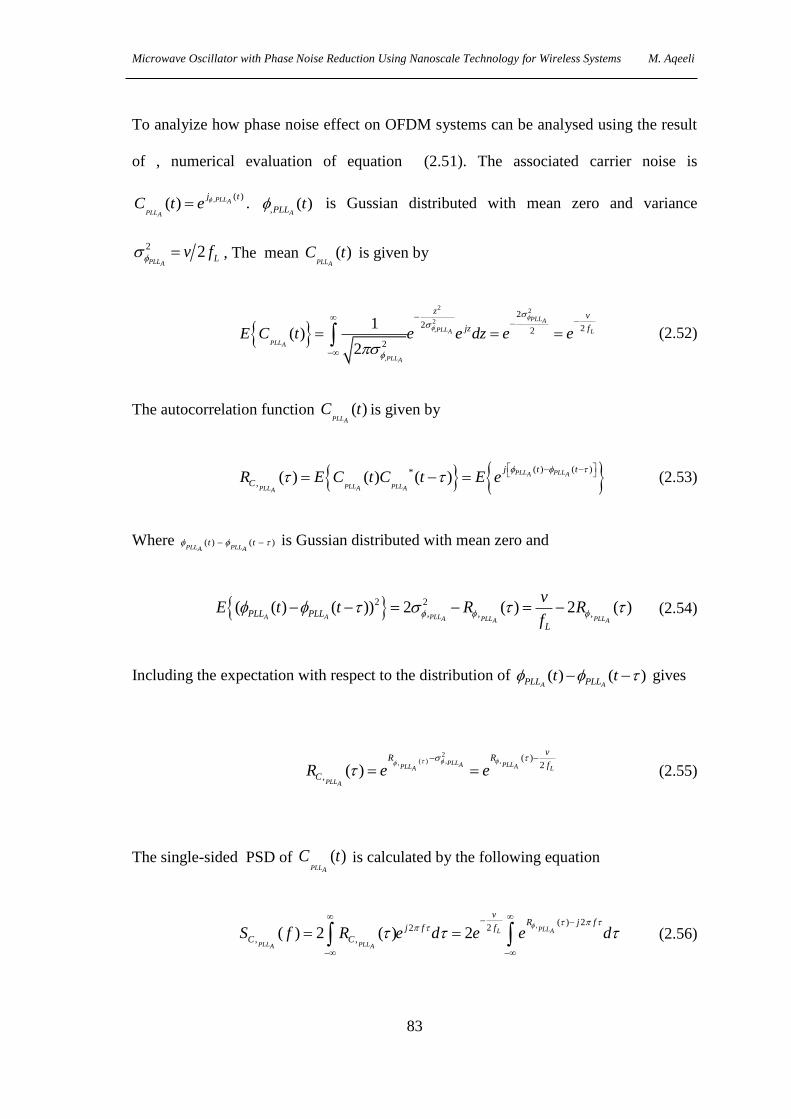
Microwave Oscillator with Phase Noise Reduction Using Nanoscale Technology for Wireless Systems M. Aqeeli
83
To analyize how phase noise effect on OFDM systems can be analysed using the result
of , numerical evaluation of equation (2.51). The associated carrier noise is
, ( )( ) PLLA
PLLA
j tC t e .
, ( )APLL t is Gussian distributed with mean zero and variance
2 2PLLA
Lv f , The mean ( )PLLA
C t is given by
2
2
2
,
,
2
2 22
2
1( )
2
PLLA
PLLA L
PLLA
PLLA
zv
fjzE C t e e dz e e
(2.52)
The autocorrelation function ( )PLLA
C t is given by
( ) ( )*
, ( ) ( ) ( )PLL PLLA A
PLL PLLPLL A AA
j t t
CR E C t C t E e
(2.53)
Where ( ) ( )PLL PLLA A
t t is Gussian distributed with mean zero and
2 2
, , ,( ( ) ( )) 2 ( ) 2 ( )A A PLLA PLL PLLA A
PLL PLL
L
vE t t R R
f (2.54)
Including the expectation with respect to the distribution of ( ) ( )A APLL PLLt t gives
2,( ) ,,
( )2
, ( )PLL PLLA APLLA L
PLLA
vRR
f
CR e e
(2.55)
The single-sided PSD of ( )PLLA
C t is calculated by the following equation
, ( ) 222
, ,( ) 2 ( ) 2 PLLL A
PLL PLLA A
vR j f
fj f
C CS f R e d e e d
(2.56)
Microwave Oscillator with Phase Noise Reduction Using Nanoscale Technology for Wireless Systems M. Aqeeli
84
Second–order PLLB 2.5.1.3:
The closed loop transfer function for the second-order PLL is as follows:
2
2 2
2( )
2
n n
n n
sH s
s s
(2.57)
Where is the damping factor which is equal to 0.707 and n is the loop natural
frequency. The sigle-sided PSD of the phase noise ( )PLLB t is represented by the
following equation
22 2
, 2 4 4( ) ( 2 ) ( ) 1 ( 2 )
2 ( )free oscPLLBC
n
v vfS f G j f S f H j f
f f f
(2.58)
Where / 2n nf is a measure of the loop bandwidth. The variance of ( )BPLL t is
calculated as follows
,
2
,
0
( )2 2PLL BB
PLL
n
vS f df
f
(2.59)
The autocorrelation of the ( )BPLL t can be calculated by the following equation
2
, 4 4( )
2 ( )B
j f
PLL
n
vR e df
f f
(2.60)
The associated carrier noise is , ( )( ) PLLB
PLLB
j tC t e , the mean value can be calculated as
follows:

Microwave Oscillator with Phase Noise Reduction Using Nanoscale Technology for Wireless Systems M. Aqeeli
85
2
2
2
,
,
2
2 2 22
2( )
2
PLLB
PLL nB
PLLB
PLLB
z v
fjzvE C t e e dz e e
(2.61)
The autocorrelation of the ( )BPLLC t is calculated by the following equation
2,( ) ,,
( )2 2
, ( )PLL PLLB BPLLB
PLLB
vRR
fn
CR e e
(2.62)
The single-sided PSD of the phase noise ( )BPLLC t is represented by the following
equation
, ( ) 222
, ,( ) 2 ( ) 2 PLLL B
PLL PLLB B
vR j f
fj f
C CS f R e d e e d
(2.63)
A summary of the statistical measures that is used to calculate the effective SNR for
several compensation schemes is presented in Table 2-1. If the phase noise model is not
specified ( )t and ( )C t are used to represent the carrier noise and the phase noise by
ignoring the subscripts. It is also the same for ( )R , ( )CR 2
, ( )S f and ( )CS f [36].

Microwave Oscillator with Phase Noise Reduction Using Nanoscale Technology for Wireless Systems M. Aqeeli
86
Table 2-1 Statistical measure for different types of phase noise [36]
Outer
Diameter
Free-
running
Oscillator
First-order PLL
Second-order PLL
2
-
2 L
v
f
2 2 n
v
f
( )R
-
2
2 22 ( )
j f
L
ve df
f f
, ( ) 22
2 PLLL A
vR j f
fe e d
( )CR v
e
, ( )2PLLA L
vR
fe
, ( )2 2PLLB n
vR
fe
( )S f 2
v
f
2 2( )L
v
f f
2
4 42 ( )n
vf
f f
( )CS f 4 2
4
(4 )
v
f v
, ( ) 22
2 PLLL A
vR j f
fe e d
, ( ) 2
2 22 PLLn B
vR j f
fe e d
( )PLLB
E C t
0
4 2 n
v
fe
, ( )2 2
PLLBn
vR
fe
2.6: Phase noise models
The well-known Leeson’s model for phase noise is based on this method. Assuming
that phase noise as a small perturbation, Leeson linearises the oscillator circuit around
the steady-state point, in order to obtain a closed-form formula for phase noise. While
often of great practical importance, Leeson’s formula has two major defects, in that it
cannot correctly describe the up-conversion of the low-frequency flicker noise
components around carrier phase noise, and it also predicts infinite phase noise power.
Hajimiri and Lee [16] used a linear time-variant model for the oscillator, in order to
propose a phase noise analysis method which explains this up-conversion phenomenon,
though it fails to predict correctly phase noise at frequency offsets very close to the
Microwave Oscillator with Phase Noise Reduction Using Nanoscale Technology for Wireless Systems M. Aqeeli
87
carrier. To overcome this problem, a non-linear analysis is required such as the
harmonic-balance and Monte Carlo methods, which are widely used in CAD
simulations. Recently, Demir presented a general method that can correctly predict the
spectrum of phase noise; however, it is more suitable for numerical calculations.
Despite its simplicity, Leeson’s phase noise model is of great practical importance, as it
provides useful design insights for low phase noise oscillators. In this section, Leeson’s
phase noise model is discussed and generalised to oscillators using complex resonant
circuits, as they are the subject of this thesis.
2.6.1: Leeson’s time-invariant (LTI) phase noise model
This approach, known as Leeson’s model, consists of a linear amplifier described with
noise figure, F, and a simple LC resonator with a finite quality factor Q0, as illustrated
in Figure 2.8. Leeson showed that for an LC oscillator, the unloaded quality factor of
the resonator is a critical parameter in determining phase noise performance [38]. In the
Leeson model, two main noise sources are considered: white noise and flicker noise.
Both noise sources modulate the oscillator phase, and therefore the signal’s
instantaneous frequency (as the frequency is a derivative of the phase). Thus, the
oscillator undergoes AM-PM noise conversion. The phase of the signal is modulated
with rates ( m )proportional to the frequency components of each of the noise sources.

Microwave Oscillator with Phase Noise Reduction Using Nanoscale Technology for Wireless Systems M. Aqeeli
88
∆𝜙𝑖𝑛 ∆𝜙𝑜𝑢𝑡
flicker noiseWhite noise
Resonator
R
LC
Figure 2.9 Leeson’s Phase Noise Model [38]
If that rate is small, flicker noise becomes the main phase modulating source, whereas a
white noise source becomes dominant at higher m . Leeson expressed the integration of
these two noise sources in terms of double sideband relative power spectral density,
represented as:
32( ) 1m
m
FkTS
Ps
(2.64)
where k is Boltzmann’s constant, F is a noise factor of the amplifier, T is the
temperature in Kelvins, Ps is a carrier signal power and 3 is the frequency for which
the level of a flicker noise is similar to the white noise, referred to as the ‘corner
frequency’.
The noise factor of the amplifier is realised as the signal-to-noise ratio on the output of
the amplifier to the signal-to-noise ratio (SNR) at its input. Equation (2.63) shows that
Lesson proposed a single noise source, thus demonstrating the power spectral density of

Microwave Oscillator with Phase Noise Reduction Using Nanoscale Technology for Wireless Systems M. Aqeeli
89
the phase uncertainty of the LC tank oscillator, . The LC tank acts as a low pass filter
which attenuates signals that are offset from the resonant frequency; this attenuation is
proportional to half of the bandwidth of the resonator:
01/ 2
02BW
Q
(2.65)
The power spectrum density of the out phase fluctuation on the amplifier out is found
from the following relation:
1/ 2
0
2
1/ 2
2( ) ( )
m
m
out m mBWm
BWS S
(2.66)
From equation (2.65), when m is greater than the resonator 1/ 2BW , frequency
variations are attenuated. If the power spectrum density of the phase variation is equal
to ( )S , total phase noise is described as follows [38]:
2 2 2
3 0 0 3 0 3
2 3 2
0 0 0
2 1 2 1 1( ) 1 1 1
4 4 4m
m m m m m
FkT FkTS
Ps Q Ps Q Q
(2.67)
Equation (2.67) indicates that lesson’s model considers four different noise sources. The
first one is up-converted flicker noise, which is proportional to 1/ 3
m . The second one is
thermal FM noise and is proportional to 1/ 2
m . The third one is flicker noise, which

Microwave Oscillator with Phase Noise Reduction Using Nanoscale Technology for Wireless Systems M. Aqeeli
90
demonstrates the noise floor, and the last source is related to the performance of the
oscillator. If the LC resonator has a low 3 or a low quality factor value Q0 and the
1/ 2BW is greater than the flicker noise corner, the phase noise spectrum consists of three
main components, as shown in Figure 2.10, which contain all the parameters of the
noise presented in equation (2.44)[38]. If the LC resonator has a high 3 or a high
quality factor value Q0, the phase noise spectrum, presented in Figure 2.11, represents
the spectrum of a conventional LC oscillator.
According to this model, in order to reduce the phase noise of an oscillator or a voltage-
controlled oscillator, some pre-conditions are required. First, the signal power of PS
must be large enough. When the amplitude of the oscillation is large, the signal-to-noise
ratio (SNR) improves, which in turn leads to lower phase noise. Secondly, the quality
factor of the resonator must be large to decrease the resonator 1/ 2BW . Thirdly, the flicker
corner frequency 3 must be low, which will reduce noise from 1/ 3
m and 1/ m .
Consequently, phase noise close to the carrier is reduced. However, Lesson’s model
contains some shortcomings. Firstly, this model presented with a bases that the
amplifier will presumably performed linearly, but this not true in reality. Secondly, the
model deals with an LC feedback oscillator only and does not cover the performance of
other oscillators, such as ring oscillators. Finally, important parameters must be known
prior to making any calculations, such as corner frequency, the power of the signal and
the noise factor.

Microwave Oscillator with Phase Noise Reduction Using Nanoscale Technology for Wireless Systems M. Aqeeli
91
1k 10k 100k 1M 10M 100M 1G 10G
-300
-280
-260
-240
-220
-200
-180
-160
-140
-120
-100
-80
-60
-40
-20
0
20
40
SS
B P
ha
se
No
ise
(d
Bc/H
z)
Frequency offset (Hz)
White noise
Total noise
mf3
mf
2
mf
Figure 2.10 Phase noise model of an LC feedback oscillator with low fm or low Q0
1k 10k 100k 1M
-200
-180
-160
-140
-120
-100
-80
-60
SS
B P
ha
se
No
ise
(d
Bc/H
z)
Frequency offset (Hz)
White noise
Total noise
mf
3
mf
2
mf
Figure 2.11 Phase noise model of an LC feedback oscillator with high fm or high Q0
Microwave Oscillator with Phase Noise Reduction Using Nanoscale Technology for Wireless Systems M. Aqeeli
92
2.6.2: Time-variant (TV) Hajimiri and Lee model.
The Hajimiri and Lee Model is conducted to demonstrate phase noise, particularly the
up-conversion of low frequency noise. The presented time-variant model has the
capability of an assessment of the effects on phase noise of both of cyclostationary and
the stationary noise sources. In addition to that it makes explicit predictions of the
relationship between waveform shape and 1/f noise up-conversion. The Hajimiri and
Lee model (HLM) [22] presents several major claims in relation to its accuracy and
explanatory power, although these claims have been proven to be incorrect. The HLM
rule approach presents how 1/f noise up-converts into close-in phase noise. In addition,
it resembles the procedures and methods used to restrain the mentioned up-conversion.
The theory conciliates cyclo-stationary noise origin sources, highlighting important
design parameters. With the HLM assumption, an amplifier introduces the same amount
of noise equally over a period of oscillation. In general, though, this is not true, since in
each cycle a standard LC resonator receives energy from the amplifier in the form of
short pulses. Noise is also injected into the tank during this short period of time.
Therefore, the phase modulation of the oscillator signal caused by noise depends also on
the time at which the noise has been introduced to the circuit. As a result, oscillator
behaviour in the presence of noise is time-variant as opposed to the HML approach.
This problem was recognised and described by Hajimiri and Lee [19]. In general, if a
pulse perturbation (or any signal including noise) is injected into an oscillating
resonator, it causes variations in both amplitude and phase. If the perturbation occurs
when an oscillation reaches its peak magnitude, the amplitude of the signal is changed,
albeit the phase is not affected. Conversely, if the same perturbation is injected during
the zero crossing, the phase changes instantly but the amplitude does not. Thus, it has
Microwave Oscillator with Phase Noise Reduction Using Nanoscale Technology for Wireless Systems M. Aqeeli
93
been seen that the phase noise of an oscillator depends on the time at which the noise is
introduced to the resonator. In order to describe the performance of phase fluctuations,
Hajimiri and Lee proposed the impulse sensitivity function (ISF), which is measured as
a relative phase change to a signal period for multiple injection instants of the single test
pulse of a magnitude of electrical charge. The ISF equates to zero when the perturbation
is applied at oscillation peak, and it approaches the maximum value when the pulse is
introduced during zero crossings. At the very moment the ISF is deduced it is extended
in terms of a Fourier series with real coefficients, which are then used to express a phase
noise equation in a logarithmic scale [22]:
2 2 2 21/0
2 3 2 2
max max
. / /( ) 10log . .
4 2
fn RMS nm
m m
c i iS
q q
(2.68)
where C0 is the first coefficient of the Fourier expansion of ISF, 2 /ni is the noise
power spectrum density of a single source, qmax is the maximum charge stored in a tank
capacitor, m is an offset frequency from the carrier, 1/ f represents the flicker corner
frequency of an amplifier and ΓRMS is an RMS value for a periodic function Γ(x).
Hajimiri and Lee noted that even though oscillators are non-linear, phase fluctuations
are proportional to the magnitude of charge injected into the resonator by noise sources.
2.6.3: Design implications and limitations of the Hajimiri-
Lee model
The main advantages of the Hajimiri-Lee approach lie in the ability of this model to
possess the non-linear effects existing in practical oscillators. From equation (2.67) it
can be seen that the resulting phase noise involves the effects of non-linear distortion

Microwave Oscillator with Phase Noise Reduction Using Nanoscale Technology for Wireless Systems M. Aqeeli
94
created in the oscillator. This qualitative derivation would not be achieved by
implementing the simple Leeson model. The main drawback of this method is the long-
winded calculation of ISF, applicable only to a defined circuit, and it fails to apply
accurately phase/frequency/modulation up-conversion produced by any capacitances
and non-linear time constants. Due to the fact that feasible oscillators present these
types of effects, it is evaluated as a model shortcoming in the specification. In addition,
as indicated in [39], a precise analytical derivation of Γ(x) does not exist, and therefore
it has to be solved numerically. Furthermore, the amplitude of the testing impulse is not
specified explicitly, and so additional testing is needed to verify linearity between phase
fluctuations and the charge.
2.7: The effect of phase noise in wireless
communication and radar systems
The impact of phase noise in any system is one of the most important subjects when
talking about phase noise in general, or VCO phase noise specifically. Oscillator phase
noise in wireless transceivers limits the overall performance of communication systems
in a variety of ways. Phase noise directly affects short-term frequency stability, bit-
error-rates and adjacent channel interference [40]. To explain how significant phase
noise is in wireless communications systems, assume a comprehensive receiver, as
depicted in Figure 2.12, which comprises a low noise amplifier, a down-conversion
mixer and a bandpass filter [41]. The LO supplying the transporter signal to the mixer is
installed in a frequency synthesiser. If the output of the LO becomes corrupted or
includes phase noise, then the down-converted element will be corrupted.

Microwave Oscillator with Phase Noise Reduction Using Nanoscale Technology for Wireless Systems M. Aqeeli
95
×
LO
Mixer
LNA BPF
Adjacent
Channel
Phase Noise
f (Hz)
LO LO
Figure 2.12 The effect of phase noise on wireless receivers [40]
On the other hand, from a practical point of view, the targeted signal might be
accompanied by a huge interferer in an adjacent channel, in which case the LO
demonstrates finite phase noise. When mixing two signals with the output of the LO,
the down-converted band formulates two overlapping spectra, and the required signal
will be affected by the considerable amount of noise caused by the tail of the interferer.
Figure 2.13 depicts the impact of phase noise on the transmit direction.
f2
Nearby
Transmitter
Wanted Signal
f (Hz)f1
Figure 2.13 The effect of phase noise on the transmit path. The nearby transmitter’s phase noise might
overwhelm the weak wanted signal
Microwave Oscillator with Phase Noise Reduction Using Nanoscale Technology for Wireless Systems M. Aqeeli
96
Consider a noiseless receiver being used to detect a low power signal at ω2, and on the
other hand a very close and powerful transmitter generating a signal at ω1 with a large
phase noise value. In this instance, the required signal will be affected or corrupted by
the phase noise tail of the interfering transmitter. The point that needs to be focused on
in this example is that the variation between the two frequencies, ω1 and ω2, can be as
low as a few tens of kilohertz, while each of these individual frequencies is nearly
several GHz. Subsequently, the LO output spectrum needs to be considerably sharp,
with an extremely minimum phase noise value. In fact, LO phase noise affects the
efficiency of communication and radar systems [42], in that it limits the performance of
communications systems and radar range and, more importantly, its detection
capabilities. In the case of a fast-moving target, and the Doppler shift is around several
kHz. Therefore, the reflected signal is going to be above the phase noise level of the LO
in the receiver. Conversely, in the case of a slow-moving target for which the Doppler
shift is around several tens of hertz, the reflected signal cannot be detected, as it is
buried in the phase noise of the local oscillator.
2.8: Phase noise measurement
Phase noise is the most important parameter in VCO design. Achieving very low phase
noise requires important attention. A primary objective of this research is to analyse
performance issues associated with noise. One way of doing this is to measure phase
noise directly using a spectrum analyser. Inherently, it is only possible to measure phase
noise of a signal by using a system which has equal or better noise performance [25].
Different kinds of methods are available for phase noise measurement, and
sophisticated measurement systems in the market, based on the depicted technique, have
Microwave Oscillator with Phase Noise Reduction Using Nanoscale Technology for Wireless Systems M. Aqeeli
97
been available for a long time. Some cases use discrete instrumentation systems,
including low noise signal generators [43].
Recent advances in digital signal processing have implemented cross-correlation
method, built-in phase noise measurement equipment. These modern solutions involve
employing signal source analyser equipment, assigned to characterise devices such as
oscillators. The simplest way of achieving this in many test equipment and calibration
laboratories is to use a spectrum analyser to measure the phase noise of a signal.
Nowadays, many spectrum analysers come equipped with phase noise measurement
options. The spectrum analyser which has the ability to measure phase noise is a
compact instrument that examines analyser’s phase noise and that of the signal. This
type of source is not valuable in the ideal case; on the other hand, the measured noise
value will be not correct. As a result, phase noise performance becomes a critical
parameter when choosing a signal source for the calibration of a spectrum analyser. The
technique involves integrating two single-channel reference sources and performing
cross-correlation operations between the outputs for every individual channel [25].
2.9: Chapter summary
In this chapter the basic oscillator theory has been presented. Oscillators are non-linear,
time-varying systems due to the presence of large and periodic signals within their
circuits. This makes phase noise analysis in oscillators a challenging task which has
been an area of investigation for several decades. In a digital communication system,
phase noise can cause a lower noise margin. In OFDM applications, a wide bandwidth

Microwave Oscillator with Phase Noise Reduction Using Nanoscale Technology for Wireless Systems M. Aqeeli
98
is divided into sub-channels. The phase noise leads to inter carrier interference and as
result a degradation in the digital communication systems. In any receiver, the effects of
phase noise introduced by the local oscillator can be improved through the design of the
oscillator itself. However, this might not be easy and will associate with an increase in
the cost. Hence, the importance of determining how much a receiver can remains
unaffected from phase noise while maintaining the targeted operation.

Microwave Oscillator with Phase Noise Reduction Using Nanoscale Technology for Wireless Systems M. Aqeeli
99
System Design Chapter 3:
Consideration of Wideband
VCOs
3.1: Introduction
Generally, modern multiband mobile radio transceivers use various VCOs to meet the
requirements of up- and down-conversions. Implementing separate VCOs would cause
a huge increase in the size of the RF section and furthermore would increase overall
costs. To resolve this problem, an integrated radio transceiver with a broadband VCO
can be used. Recently, work has been published on a high standard RF CMOS VCO
with excellent features. This chapter focuses on system design considerations in fully
integrated transceiver solutions and explores the aforementioned broadband RF CMOS
VCO. By itself‚ a VCO incorporates phase noise‚ tuning range, harmonics level, output
power and power consumption.

Microwave Oscillator with Phase Noise Reduction Using Nanoscale Technology for Wireless Systems M. Aqeeli
100
3.2: Radio architecture and frequency planning
considerations
Designing a multiband radio transceiver requires an optimised frequency plan to
minimise the die area and to maximise component sharing. Integrated receivers
overwhelmingly use either low-IF or wideband-IF, as depicted in Figures 3.1-3.2, which
represent wideband IF and low-IF receiver architectures using wideband VCOs for
several applications, where ‘divide-by-2’ and ‘divide-by-4’ devices are implemented to
produce quadrature LO signals [1]. If the VCO operates at a frequency which is higher
than the desired LO frequency, it will have advantages for completely integrated direct
conversion radio applications [2], i.e. it will unbuckle a number of direct conversion
design parameters, for example the excessive frequency pulling of the VCO by injection
locking, load pulling and self-mixing of the LO and RF signals. Quadrature‚ I/Q‚ LO
signals are produced accurately by quadrature/2 circuits.
VCO
(3.6-4.3 GHz)
Mixer
LNABPF
Mixer
×
×
/4
Mixer
LNABPF
Mixer
×
×
GSM 900
MHz
GSM 1800 MHz/1900 MHz/
WCDMA
/2
I
I
Q
Q
Figure 3.1 Direct conversion receiver for multi-standard cellular application

Microwave Oscillator with Phase Noise Reduction Using Nanoscale Technology for Wireless Systems M. Aqeeli
101
A WLAN receiver operating at a frequency of 2.4 GHz can be designed with a
wideband IF or direct conversion, as depicted in Figures 3.2 (a) and (b)‚ respectively.
Figure 3.2 (a) shows the direct conversion WLAN receiver implementing a VCO at an
operating frequency of 5 GHz, as well as the divide-by-2 circuit for quadrature LO [1].
Figure 3.2 (b) depicts a receiver architecture with a two-step down-conversion
implementing a first LO frequency at 3.2 GHz which interprets input signals at
oscillating frequencies ranging between an RF frequency of 2.4 GHz and an IF
frequency of 800 MHz. Quadrature LOs at a frequency of 800 MHz are produced by a
quarter circuit from the exact wideband VCO. Image frequency is situated at 4 GHz [1]
Consequently‚ the incoming RF and the image signals are dissociated by 1.6 GHz,
which permits for on-chip filtering of the image signal. The wideband IF receiver helps
the VCO to operate in a bandwidth between 3.2 and 3.3 GHz.
Mixer
LNABPF
Mixer
×
×For WLAN
/2
I
Q VCO
Tuning Range: (4.8-5.0GHz) f0 =2.4 GHz
IF Receiver
(a)
Mixer
Mixer
LNABPF
×
×
/4
I
Q
×VCO
Tuning Range: (3.2-3.3 GHz) f0 =2.4 GHz For WLAN
Direct conversion Receiver
(b)
Figure 3.2 Receiver architectures for WLAN applications at the 2.4 GHz ISM band
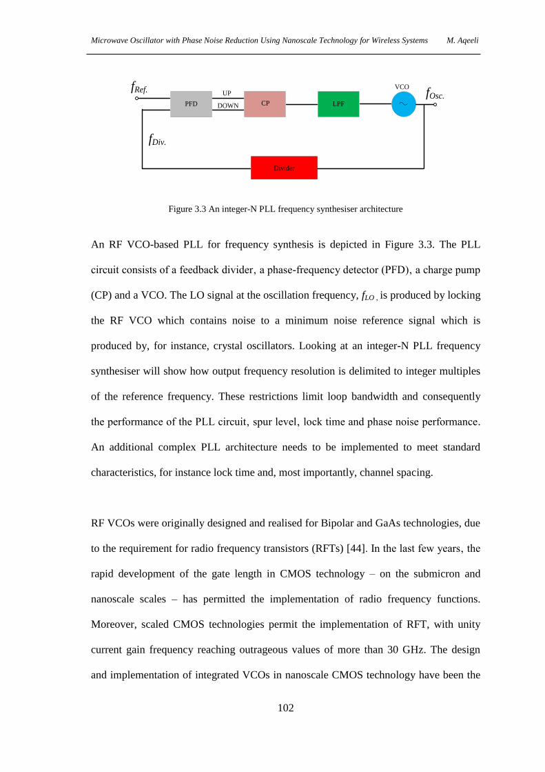
Microwave Oscillator with Phase Noise Reduction Using Nanoscale Technology for Wireless Systems M. Aqeeli
102
Divider
LPFCPPFD
VCOUP
DOWN
fOsc.fRef.
fDiv.
Figure 3.3 An integer-N PLL frequency synthesiser architecture
An RF VCO-based PLL for frequency synthesis is depicted in Figure 3.3. The PLL
circuit consists of a feedback divider‚ a phase-frequency detector (PFD)‚ a charge pump
(CP) and a VCO. The LO signal at the oscillation frequency, fLO , is produced by locking
the RF VCO which contains noise to a minimum noise reference signal which is
produced by, for instance, crystal oscillators. Looking at an integer-N PLL frequency
synthesiser will show how output frequency resolution is delimited to integer multiples
of the reference frequency. These restrictions limit loop bandwidth and consequently
the performance of the PLL circuit‚ spur level‚ lock time and phase noise performance.
An additional complex PLL architecture needs to be implemented to meet standard
characteristics, for instance lock time and, most importantly, channel spacing.
RF VCOs were originally designed and realised for Bipolar and GaAs technologies, due
to the requirement for radio frequency transistors (RFTs) [44]. In the last few years‚ the
rapid development of the gate length in CMOS technology – on the submicron and
nanoscale scales – has permitted the implementation of radio frequency functions.
Moreover, scaled CMOS technologies permit the implementation of RFT, with unity
current gain frequency reaching outrageous values of more than 30 GHz. The design
and implementation of integrated VCOs in nanoscale CMOS technology have been the
Microwave Oscillator with Phase Noise Reduction Using Nanoscale Technology for Wireless Systems M. Aqeeli
103
flagship topic of ongoing research [45-48]. Highly sophisticated and fully integrated
PLLs have been reported in many researches [49, 50]. The advanced scaling of the
channel length of the pMOS and the nMOS transistor conducted with a lessening in the
breakdown voltage and turned out to be limiting the maximum supply voltage.
Reducing the supply voltage presents new challenges in the design, simulation and
integration of LC-VCOs at frequencies measured in GHz, by minimising the obtainable
controlling voltage. Focusing on the subject of integrating LC-VCOs operating in RF
bands on the sub-micron CMOS technology scale, consistent with other parameters,
raises the following two issues. The first is that the output spectral purity of proposed
VCO ought to be preserved in an integrated circumference together with an assortment
of noise sources from other digital devices and signal sources, due to poor isolation and
cross-talking on the die chip. Secondly, supply voltage scaling in sub-micron CMOS
technology creates complications for the wideband tuning range operations because of
the need to reduce tuning voltage [1].
3.3: The problem of spectral purity
A wireless transceiver, designed and fabricated on the same single chip implementing
CMOS technology, comprises analogue and digital circuits on the substrate. These
digital circuits will become a source of noise in the substrate, and this noise may cause
coupling between blocks in various mechanisms. The first type is the coupling through
the substrate, while the second one is the coupling through the supply, and last but not
least is the coupling through the signal lines. With regard to noise coupled to the VCO
control line‚ bias lines and supply sources, this type of noise will be transformed into
noise sidebands surrounding the oscillation frequency through AM‚ FM and AM-FM

Microwave Oscillator with Phase Noise Reduction Using Nanoscale Technology for Wireless Systems M. Aqeeli
104
transformation mechanisms. Focusing on AM noise influences, it can be said that this
type of noise is less important for the close-in spectral purity of VCOs in contrast to the
influences of FM or PM noise. In addition‚ AM noise can be overcome by using any
type of limiter. On the other hand‚ AM noise is predominantly transformed into FM
noise through a process called ‘AM-FM conversion’. AM-FM transformation noise and
FM noise are preferably searched for integration considerations.
3.4: FM noise contributions
Noise linked to the tuning voltage used across any type of varactor, whether nMOS,
pMOS or diodes implemented in the LC tank of VCOs, will change the tank’s
capacitance and, as a result, the resonant frequency. This can be observed as a
frequency modulation noise (FMN) mechanism which illustrate any low frequency
noise surrounded the oscillation frequency. For any noise source with an rms voltage
value on the VCO control line, phase noise is characterised using narrowband FM
approaches by applying the following equation ]:
2
2( ) 10log 10log
2
VCO nnoiseVCNT m
carrier m
K VPL f
P f
(3.1)
Phase noise produced from the control line to the PLL output might be reduced through
making the gain of the VCOs as small as possible. Noise sources in the control line are
CP current noise and the thermal noise of the loop filter resistor, further to any other
noise linked by signal routing and the substrate. Generally‚ the FM noise mechanism is
amenable to whatever noise source is modulating or varying the frequency of the

Microwave Oscillator with Phase Noise Reduction Using Nanoscale Technology for Wireless Systems M. Aqeeli
105
oscillation. A VCO’s output frequency is responsive to supply voltage or biasing current
variations. Any noise accompanied by the supply voltage or the biasing current will
furthermore participate in a similar way to the phase noise of VCOs through the FM
noise mechanism. Therefore, Leeson’s equation can be expanded to include the
contributions of this noise as follows:
2 2 2 2
2 2 2
2 0( ) 10log 1
2 2 2 2
VCO VCO IBkm VCNT VDD
L m m m m m
K K KfFkT fL f S S
Ps Q f f f f f
(3.2)
where SVCNT and SVDD are the voltage noise spectral densities of the voltage supply and
the tuning voltage in V2/Hz, respectively. KVDD and KVCO are defined as VCO gain in
relation to voltage supply and tuning voltage ‚ respectively, and the gain of the VCO in
relation to the bias current variations, KIB. Thus‚ the supply gain or sensitivity and the
bias of the VCO should be reduced as much as possible to achieve low noise
performance. Supply and bias noise can be reduced by adapting q filtering technique
without affecting the dynamics of the PLL circuits, which is not possible to accomplish
for noise accompanied by the tuning control input of the VCO [1]. Circuit and layout
design techniques represent main functions involved in minimising noise coupled to the
controlling line on the die chip.
3.5: AM-FM conversion noise contribution
The effective and capacitance performances of any varactor rely on the amplitude of the
oscillation and DC voltage. Different noises coupled to bias, supply and substrate
improve the oscillation amplitude of VCOs. Taking a differential LC-VCO or an LC-
oscillator as an example, these two types of oscillator up-convert low frequency bias

Microwave Oscillator with Phase Noise Reduction Using Nanoscale Technology for Wireless Systems M. Aqeeli
106
noise into AM sidebands. These up-conversions are performed around the frequency of
the oscillation. Generally‚ AM noise contributes in a small way to close offset
frequencies in comparison to FM or PM noise contributions. In addition‚ this noise can
be rejected by using a limiter circuit. However‚ AM noise connected to resonator
modulate as well the effectiveness capacitance of any varactor, which as a consequence
transforms AM noise into FM noise. It can be stated confidently that the sidebands of
FM noise cannot be distinguished from phase noise‚ and a limiter circuit cannot
suppress phase noise or FM [39]. AM-FM noise can be calculated by implementing the
approximation of the FM narrowband [39]:
2
,
2( ) 10log
2
AM FM n A
AM FM m
m
K V ML f
f
(3.3)
where KAM-FM is the transformation gain of AM-FM in V/Hz. Vn, AM is the rms voltage
spectral density AM noise in V Hz . The AM-FM transformation gain is determined
as:
eff
AM FM
CK
A
(3.4)
where Ceff is effective MOS capacitance’s, A is amplitude. Since 0 1 effLC , then:
1
2
effoAM FM
eff
CK
C A
(3.5)
The effective MOS capacitance’s, Ceff sensitivity to the amplitude of the oscillation is
presented by [42]:

Microwave Oscillator with Phase Noise Reduction Using Nanoscale Technology for Wireless Systems M. Aqeeli
107
2
max min
2
21
eff DC DCC C C V V
A A A
(3.6)
From Equations 3.5 and 3.6:
max minAM FMK C C (3.7)
Equation 3.7 proposes that a wide tuning range results in a huge AM-FM gain‚ and in-
turn greater AM-FM noise transformation. An identical connection for a P n junction
diode can be derived if the diode is implemented as a varactor in an oscillator or a VCO.
3.6: Spurious sidebands
Any compulsive signal on the control line with frequency fs, for example a reference
signal supplying through from the CP circuit output and the crystal clock connected to
the controlling line‚ ought to be up-converted as discrete sidebands around specific
frequencies of oscillation 0 sf f . These discrete sidebands are nominated as reference
spurs, which are caused by the reference signal connected to the tuning line. These
spurious sidebands’ magnitudes can be calculated in relation to the carrier magnitude,
by using Equation 3.1 throughout and substituting Vn with 2nV for a periodic signal:
2
2( ) 10log 10log
4
spur VCO s
spur m
carrier s
P K VL f
P f
(3.8)
Spurious VCO sidebands can be reduced greatly by decreasing the gain of the VCO,
KVCO.

Microwave Oscillator with Phase Noise Reduction Using Nanoscale Technology for Wireless Systems M. Aqeeli
108
Any spurious sidebands which appear due to the on-chip crystal clock may also be
minimised by implementing the highest possible crystal frequency‚ fXCO. The reference
frequency of the PLL can be produced by implementing a divider from the crystal clock
signal. An alternative method for reducing the spurious sideband involves isolating the
tuning line. On-chip loop filter applications are not constantly conceivable when the
values of the component are too large for on-chip physical implementation. The off-chip
position of the loop filter generally results from routing lines to the VCO, especially if
longer lines are used in the circuit‚ which means that great attention must be given to
the circuit layout.
3.7: Supply voltage effects
VCO tuning ranges should cover all selectable channels within the required CP output
voltage or VCO tuning voltage in the existence of PVT variations. CP and VCO
connections through a loop filter are depicted in Figure 3.4(a). The required tuning
curve is depicted in the coloured area of Figure 3.4(b). However, obtaining such tuning
curves presents challenges in CMOS sub-micron technology, because of the scaled
supply voltage which limits the targeted bandwidth or the tuning voltage. Nevertheless,
by implementing a small tuning voltage range, it is possible to achieve a wide tuning
range when implementing nMOS or pMOS devices such as varactors [14, 25, 51-53].
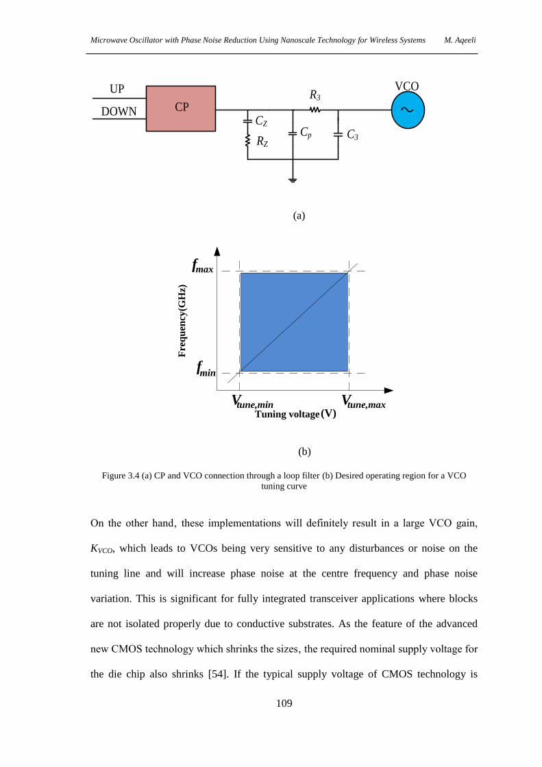
Microwave Oscillator with Phase Noise Reduction Using Nanoscale Technology for Wireless Systems M. Aqeeli
109
UP
DOWN CP
VCO
CZ
RZ
R3
C3Cp
(a)
Vtune,min Vtune,max
fmin
Tuning voltage(V)
Fre
qu
ency
(GH
z)
fmax
(b)
Figure 3.4 (a) CP and VCO connection through a loop filter (b) Desired operating region for a VCO
tuning curve
On the other hand‚ these implementations will definitely result in a large VCO gain,
KVCO, which leads to VCOs being very sensitive to any disturbances or noise on the
tuning line and will increase phase noise at the centre frequency and phase noise
variation. This is significant for fully integrated transceiver applications where blocks
are not isolated properly due to conductive substrates. As the feature of the advanced
new CMOS technology which shrinks the sizes‚ the required nominal supply voltage for
the die chip also shrinks [54]. If the typical supply voltage of CMOS technology is

Microwave Oscillator with Phase Noise Reduction Using Nanoscale Technology for Wireless Systems M. Aqeeli
110
1.2 V, an exemplary charge pump will operate at an output voltage range approximately
between (0.3 V - 1.0 V) while maintaining output transistors in saturation. .
Tuning curve non-linearity means that any gain, KVCO , will vary over the tuning
voltage, and degradation in the overall PLL performance parameters will result. In order
to obtain wideband tuning with low VCO gain, KVCO and linear tuning curves
simultaneously, the single wideband tuning curve is divided into multiple narrow sub-
bands with an adequate frequency overlap. This method can be used by employing
continuous and discrete tuning, while continuous tuning can be used by employing
either an nMOS or a pMOS varactor.
3.8: Consideration of circuit design and
implementation
This section explores circuit design considerations for wideband RF LC-VCOs and their
implementation and applications in fully integrated transceivers. A wideband LC-VCO
with sub-bands is considered an important device for communication implementation.
Inductance and capacitance switching designs for discrete tuning control are explored
for implementation and performance considerations. The resonator tank design and the
active circuit for the LC-VCO design will be detailed herein. The current biasing circuit
is a major noise source and contributes to phase noise in VCOs. Therefore, biasing
filtering techniques are important parameters which need to be investigated. Solutions
such as dynamic bias filtering is recommended for fast start-up, and it is necessary to
explore passive components which are used to form some of the LC tank of the VCO.
They are of primary importance, because they fundamentally determine two important
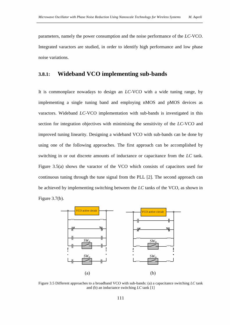
Microwave Oscillator with Phase Noise Reduction Using Nanoscale Technology for Wireless Systems M. Aqeeli
111
parameters, namely the power consumption and the noise performance of the LC-VCO.
Integrated varactors are studied, in order to identify high performance and low phase
noise variations.
3.8.1: Wideband VCO implementing sub-bands
It is commonplace nowadays to design an LC-VCO with a wide tuning range, by
implementing a single tuning band and employing nMOS and pMOS devices as
varactors. Wideband LC-VCO implementation with sub-bands is investigated in this
section for integration objectives with minimising the sensitivity of the LC-VCO and
improved tuning linearity. Designing a wideband VCO with sub-bands can be done by
using one of the following approaches. The first approach can be accomplished by
switching in or out discrete amounts of inductance or capacitance from the LC tank.
Figure 3.5(a) shows the varactor of the VCO which consists of capacitors used for
continuous tuning through the tune signal from the PLL [2]. The second approach can
be achieved by implementing switching between the LC tanks of the VCO, as shown in
Figure 3.7(b).
VCO active circuit
SWn
SWo
VCO active circuit
SWn
SWo
(a) (b)
Figure 3.5 Different approaches to a broadband VCO with sub-bands: (a) a capacitance switching LC tank
and (b) an inductance switching LC tank [1]
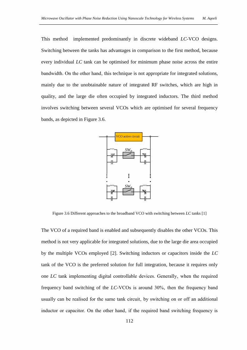
Microwave Oscillator with Phase Noise Reduction Using Nanoscale Technology for Wireless Systems M. Aqeeli
112
This method implemented predominantly in discrete wideband LC-VCO designs.
Switching between the tanks has advantages in comparison to the first method, because
every individual LC tank can be optimised for minimum phase noise across the entire
bandwidth. On the other hand‚ this technique is not appropriate for integrated solutions,
mainly due to the unobtainable nature of integrated RF switches, which are high in
quality, and the large die often occupied by integrated inductors. The third method
involves switching between several VCOs which are optimised for several frequency
bands, as depicted in Figure 3.6.
VCO active circuit
SWn
SWn
Figure 3.6 Different approaches to the broadband VCO with switching between LC tanks [1]
The VCO of a required band is enabled and subsequently disables the other VCOs. This
method is not very applicable for integrated solutions, due to the large die area occupied
by the multiple VCOs employed [2]. Switching inductors or capacitors inside the LC
tank of the VCO is the preferred solution for full integration, because it requires only
one LC tank implementing digital controllable devices. Generally‚ when the required
frequency band switching of the LC-VCOs is around 30%‚ then the frequency band
usually can be realised for the same tank circuit‚ by switching on or off an additional
inductor or capacitor. On the other hand‚ if the required band switching frequency is

Microwave Oscillator with Phase Noise Reduction Using Nanoscale Technology for Wireless Systems M. Aqeeli
113
above 30%‚ then it will become a very complex undertaking to fulfil both wideband and
low noise requirements for low phase noise at the centre frequency and low phase noise
variation in a single design [14]. Importantly, switching between VCOs or their LC
tanks is mandatory for good phase noise performance when the tuning range is equal to
or greater than 30%.
3.8.2: Switching techniques for a wideband LC-VCO
This section discusses, switching discrete values of capacitance or inductance from an
LC tank, to design a wideband VCO, and its trade-offs.
Capacitance switching 3.8.2.1:
The first proposal to extend the tuning range is to use switching capacitances. nMOS
transistor technology is implemented to design an RF switch. nMOS transistor circuits,
used to switch in and out a capacitance value of Co at high frequencies. The drain
parasitic fringe capacitance, Cd , is equal to Wsw * Cdd. The switching transistor is Wsw
and Cdd is drain fringe capacitance.
The equivalent circuits with capacitance (Co) and the switch in the OFF case are
depicted in Figure 3.7(a). Assuming that 1
.OFF dR C
and COFF, then the
impedance of the circuit will be, 0//OFF dC C C which is written as:
1( )
OFF
Z ssC
(3.9)
The equivalent circuits for capacitance (Co) and the switch in the ON state are depicted
in Figure 3.7(b). Channel resistance, RON, of the switching transistor is combined in

Microwave Oscillator with Phase Noise Reduction Using Nanoscale Technology for Wireless Systems M. Aqeeli
114
series with capacitance Co. When the case is ON, the impedance of the circuit, assuming
1
.OFF dR C
, is written as [1]:
0
1( ) ONZ s R
sC (3.10)
Resistance RON is the channel resistance of the MOS transistor‚ and it is written as
follows:
1
ON n ox GS t
WR C V V
L
(3.11)
As mentioned previously, CMOS technology continues to scale down‚ and so as a result
the RON value improves, because channel resistance is inversely proportional to channel
length. In the design consideration it should be noted that two operational parameters
need to be focused on. The first is the Q factor of the tuning circuit at the frequency
band, while the second is the ratio of the maximum capacitance to the minimum
capacitance Cmax/Cmin. It is noteworthy that the Q factor of the switched capacitance is
lowest at the situation when the switch device is ON. This quality factor can be written
as [1]:
0
1
o ON
QC R
(3.12)
where 𝜔𝑜 is the operating frequency and RON is given by 3.11. From equation 3.11 and
3.12, the quality factor can be rewritten as follows [1]:
0
sw
o
WQ
C
(3.13)

Microwave Oscillator with Phase Noise Reduction Using Nanoscale Technology for Wireless Systems M. Aqeeli
115
where Wsw is the width of the switching transistor. To obtain a maximum quality factor,
VGS-Vt=VDD-Vt and L=Lmin must be selected, according to equation (3.11). The
parameters Co and Wsw are the design variables. The tuning range is reliant on the
Cmax/Cmin ratio, since oscillation frequency is proportional to 1 LC . This ratio can be
written as [1]:
max 0
min
1sw dd
C C
C W C (3.14)
Vsw= 0
Co
Msw ROFF Cd
Co
Cd
Co
Vsw= Vdd
Co
Msw RON Cd
Co
RON
Co
(a) (b)
Figure 3.7 nMOS transistors as an RF switch: (a) VSW is low, in the OFF state, while (b) VSW is high,
in the ON state [1]
Equations 3.13 and 3.14 propose increasing the Q factor of the switched capacitance.
When the switched capacitance magnitude, Co, is specified at operating frequency, 0 ,
the width of the switching transistor‚ Wsw, is the most important design parameter to be
optimised [1]. The switched capacitance quality factor can be changed for the better by
employing a single switch device for two capacitances in a differential pattern, as
depicted in Figure 3.8. When the switch is ON, half of the resistance‚ RON, can be
added to each capacitance. In this respect, the Q factor will ameliorate twice as much as
the single-ended structure that is shown in Figure 3.7.

Microwave Oscillator with Phase Noise Reduction Using Nanoscale Technology for Wireless Systems M. Aqeeli
116
Vsw
Co MswCo
Figure 3.8 Differential capacitance switching
Differentially switched capacitances are depicted in Figure 3.9. The notable difference
between these two structures is the biasing of the MOS switch device‚ M1. Resistors R1
and R2 are implemented for DC biasing of the source and drain terminals of the MOS
switching device. The amount of these resistors must be large enough for the
operational frequency, since it is important to display high impedance for RF signals.
The operational mode of this switch is as follows: when Vsw is set to zero, then VGS -Vt
of the nMOS transistor is maximised by setting VG= Vdd and VD/S=0V [1]. The
equivalent capacitance that is seen from differential ports will take the maximum value
and lessen the frequency of operation. When Vsw is set to high, Vdd, the higher frequency
band is selected, with VG= 0V and VD/S= Vdd being voltages for the higher voltage
setting.
NP
Vsw
Co MswCo
Figure 3.9 Differential capacitance switching with biasing resistors [1]
Microwave Oscillator with Phase Noise Reduction Using Nanoscale Technology for Wireless Systems M. Aqeeli
117
The switched capacitance is implemented using either MIM (metal-insulator-metal) or
MOM (metal-oxide-metal) capacitance, as will be seen later on in this thesis.
Inductance switching 3.8.2.2:
The differential switching of inductors has the advantage of lowering parasitic
capacitance and series resistance by an approximate factor of two. Conversely,
switching the inductors comes from loss in the CMOS switch, as in the case of
switching capacitance. It is apparent that any loss in the switch is more common in the
inductor case, because the Q factor of an on-chip inductor would have been previously
lower than the Q factor of the capacitance. When switches are designed with
specifically lower series resistance, in order to eliminate deterioration of the quality of
the tank‚ then massive parasitic switch capacitance is conducted on the RF-nodes of the
tank, which leads to phase noise and high power consumption. Unfortunately, the
implementation of evenly spaced sub-bands is relatively difficult when applying
switching inductors, because essentially they demand the use of a binary-weighted
inductor switching structure which presupposes executing multiple inductors‚ Lo,
2Lo,….. nLo. The characterisation of such a structure is not a recommended task.
Moreover‚ it will take the provision of a very big die area. Thus, inductor switching
does not permit digitally controllable sub-bands [1].
The linearity of the tuning curves is difficult to controlled implementing inductor
switching with LC-VCO frequency which is proportional to 1 / p vL C C . Variable
capacitance, Cv, in the LC-resonator remains fixed when switching from a small to a
huge inductor value.

Microwave Oscillator with Phase Noise Reduction Using Nanoscale Technology for Wireless Systems M. Aqeeli
118
3.9: Wideband VCO implementation
A standard CMOS LC-VCO involves complementary, cross-coupled nMOS and pMOS
pairs, in order to realise negative resistance required to compensate for the loss of the
LC tank in an oscillator [55]. In a fully integrated circuit realisation, the differential
topology has some advantages‚ such as the rejection of substrate noise and the rejection
of common-mode supply.
3.9.1: Active circuit design
The most conventional differential cross-coupled topology is depicted in Figure 3.10.
The choice of topology depends on specifications of the LC-VCO, which are most
importantly phase noise at the centre frequency, phase noise variations at the minimum
and the maximum frequencies‚ tuning range, power consumption and the process
technology.
Vout-Vout+
Switch capacitor array
Vtune
M1 M2
Vdd
Vout-Vout+
Switch capacitor array
Vtune
M1 M2
Figure 3.10 nMOS VCO topology [1]

Microwave Oscillator with Phase Noise Reduction Using Nanoscale Technology for Wireless Systems M. Aqeeli
119
The nMOS topology depicted in Figure 3.12 facilitates a distinctive attribute, which is
higher transconductance per area in comparison to the pMOS-only topology, which is
shown in Figure 3.13.
Vdd
Vout-Vout+
Switch capacitor array
Vtune
M1 M2
Vdd
Vout-Vout+
Switch capacitor array
Vtune
M1 M2
Figure 3.11 pMOS VCO topology [1]
This is due to the higher mobility of electrons in nMOS transistors‚ and, as a result,
lower transistor capacitances ought to participate in the total parasitic capacitance of the
LC tank. On the other hand‚ the flicker noise density is lower using pMOS transistors
than nMOS devices.
With regard to the nMOS and pMOS complementary topology shown in Figure 3.12‚ it
is noticeable that the power consumption of this topology is smaller than the power
consumption of the pMOS-only or nMOS-only topologies, due to the fact that the bias
current has been reused. It can be said that a topology is applicable where there is
sufficient supply voltage for the transistors. The most obvious case applies when the
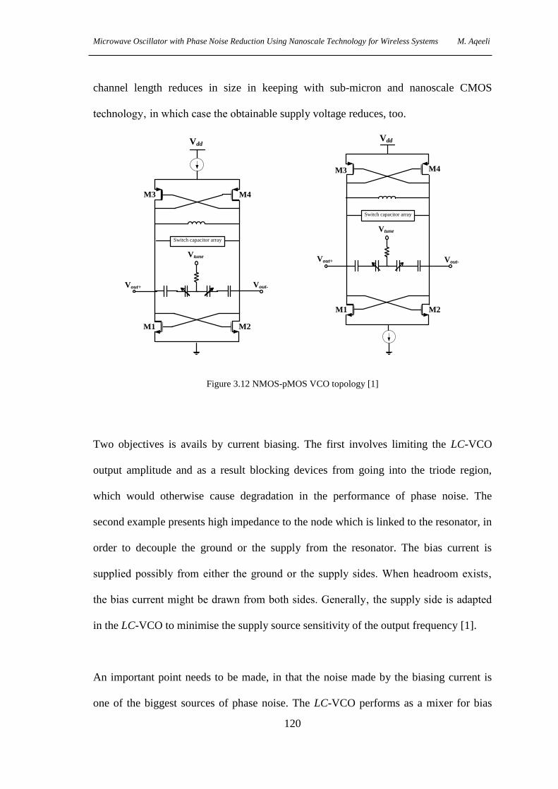
Microwave Oscillator with Phase Noise Reduction Using Nanoscale Technology for Wireless Systems M. Aqeeli
120
channel length reduces in size in keeping with sub-micron and nanoscale CMOS
technology‚ in which case the obtainable supply voltage reduces, too.
Vdd
Vout-Vout+
Switch capacitor array
Vtune
M3 M4
M1 M2
Vdd
Vout-Vout+
Switch capacitor array
Vtune
M3 M4
M1 M2
Figure 3.12 NMOS-pMOS VCO topology [1]
Two objectives is avails by current biasing. The first involves limiting the LC-VCO
output amplitude and as a result blocking devices from going into the triode region,
which would otherwise cause degradation in the performance of phase noise. The
second example presents high impedance to the node which is linked to the resonator, in
order to decouple the ground or the supply from the resonator. The bias current is
supplied possibly from either the ground or the supply sides. When headroom exists‚
the bias current might be drawn from both sides. Generally‚ the supply side is adapted
in the LC-VCO to minimise the supply source sensitivity of the output frequency [1].
An important point needs to be made, in that the noise made by the biasing current is
one of the biggest sources of phase noise. The LC-VCO performs as a mixer for bias

Microwave Oscillator with Phase Noise Reduction Using Nanoscale Technology for Wireless Systems M. Aqeeli
121
noise and transforms low-frequency bias noise into sidebands. At the drain of both
transistors M1 and M2 in in Figure 3.12, the small signal admittance is equivalent to
Gin=-gm/2 [1]. In the saturation region, MOS transconductance can be written as:
m n ox GS t
Wg C V V
L
(3.15)
where (µn Cox) is a fixed process-dependent design parameter, W is the width, L is the
length of the transistor geometry and the DC bias point, (VGS-Vt), are selected to obtain
the required gm.
A trade-off occurs between phase noise performance, the tuning range and power
savings when choosing the length and width of the transistor and bias point (VGS-Vt). In
order to decrease power consumption‚ (VGS-Vt ) must be as small as possible; therefore,
in this situation‚ (W/L) has to be increased to achieve the targeted value. This will result
in huge parasitic capacitances combining with the capacitance of the resonant tank,
which then leads to minimising the tuning range. In addition, reducing (VGS-Vt) and the
size of the transistor value will increase the tuning range, minimise power consumption
and produce a lower oscillation amplitude . .Osc OscV I In general, the minimum
oscillation amplitude will lead to high phase noise, because phase noise is inversely
proportional to the square of the amplitude of oscillation‚ 2
,. 1 .Osc ampPN V
Lowering power consumption in an LC-VCO requires immolations from the tuning
range and phase noise performance. Increasing the tuning range to its maximum level
will result in a higher power consumption value and unwanted phase noise. Minimising

Microwave Oscillator with Phase Noise Reduction Using Nanoscale Technology for Wireless Systems M. Aqeeli
122
phase noise requires a small tuning range, which enlarges the L/C ratio. In addition, it
will require the highest output amplitude, which ultimately means more power
consumption [1]. The resistance that is seen at the active circuit port, Ra, in Figures
3.12-3.14 has to be selected at least two times higher than the effective resistance of the
resonant tank, 2a mR g , in order to guarantee the start-up the oscillation in the
VCO.
3.9.2: Programmable bias current
The biasing current of the LC-VCO can be designed to be programmable, in order to
efficiently vary the core current of the LC-VCO for amplitude adjustment when the Q
factor of the resonator is small due to process variations‚ voltage supply variations and
temperature. In addition‚ the resonator Q changes across the tuning range for wider
bandwidth. During stabilised performance‚ oscillator-active devices perform as switches
– not as small signal negative resistance. The current supplied to the resonator tank is
bounded by the current mirrors in the LC-VCO bias circuit and turns into a square wave
with a peak current, Iosc. In general, for any oscillator, output is calculated
approximately by implementing the Fourier component [1] as follows:
2p osc pV I R
(3.16)
Where Vp is the peak voltage, IOsc is the current supplied to the resonator and Rp is the
equivalent tank resistance at the steady state. Equation 3.16 shows that the oscillator’s
output amplitude is originally dependent on the active device bias current and the
resonator equivalent resistance. The easiest way to keep the output amplitude of the LC-
VCO at the required level, or constant through the frequency band, is to maintain the

Microwave Oscillator with Phase Noise Reduction Using Nanoscale Technology for Wireless Systems M. Aqeeli
123
result of Osc pI R fixed. This can be implemented or accomplished in several ways. One
method is by implementing the automatic amplitude control (AAC) circuit. A detailed
explanation of the analogue and the digital AAC for LC-VCOs is presented in [1]. The
AAC circuit is required in wideband LC-VCOs to assure appropriate performance
across a broadband tuning range. Figures 3.13 and 3.16 show two different topologies
employed to obtain proper amplitude for a wideband LC-VCO. The first architecture,
which is shown in Figure 3.13, represents a digital correction circuit using an ADC
circuit, while the second architecture, shown in Figure 3.14, uses the programmable bias
block.
Ibias
VCO
Vp Vn
Programable Bias
Block
Amplitude
detector
ADC
Dig. Ctrl
IOSC
AOUT
Figure 3.13 Amplitude correction circuit with detector [1]
VCO
Programable Bias
Block
IOSC
TR(0:N)
Ibias
Figure 3.14 Amplitude correction based on tuning curve selection [1]

Microwave Oscillator with Phase Noise Reduction Using Nanoscale Technology for Wireless Systems M. Aqeeli
124
3.9.3: Bias noise filtering
A standard low pass bias filter is depicted in Figure 3.15(a). The product of b pC R
determines the noise bandwidth, which should be less than the PLL loop bandwidth
because the PLL restrains LC-VCO noise inside the PLL loop’s bandwidth. Standard
resistors and capacitors found in CMOS submicron and nanoscale technology occupy a
large die area. Figure 3.17(b) shows a proposed solution. Importantly, using a large
resistor with nMOS or pMOS transistors employs less die area than a capacitor in an
MOS device.
Vdd
M1 M2
Iout
Rb
Cb
Iin
Vdd
M1 M2
Iout
Vbf
M3
M4
Iin
Figure 3.15 Bias filtering (a) conventional low-pass bias filter (b) nMOS bias filter [1]
As a consequence‚ it is preferable to make the capacitance small and the resistance large
while retaining the product, RC fixed. MOS resistance in the triode region can be
obtained by:
1
DS n ox GS t
WR C V V
L
(3.17)
The resistance of the MOS transistor is a function of GS tV V and (W/L). Bias voltage‚
Vbf, sets the MOS transistor resistance shown in Figure 3.18. Another consideration
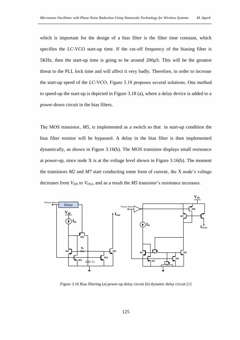
Microwave Oscillator with Phase Noise Reduction Using Nanoscale Technology for Wireless Systems M. Aqeeli
125
which is important for the design of a bias filter is the filter time constant, which
specifies the LC-VCO start-up time. If the cut-off frequency of the biasing filter is
5KHz, then the start-up time is going to be around 200µS. This will be the greatest
threat to the PLL lock time and will affect it very badly. Therefore, in order to increase
the start-up speed of the LC-VCO‚ Figure 3.18 proposes several solutions. One method
to speed-up the start-up is depicted in Figure 3.18 (a), where a delay device is added to a
power-down circuit in the bias filters.
The MOS transistor‚ M5, is implemented as a switch so that in start-up condition the
bias filter resistor will be bypassed. A delay in the bias filter is then implemented
dynamically, as shown in Figure 3.16(b). The MOS transistor displays small resistance
at power-up, since node X is at the voltage level shown in Figure 3.16(b). The moment
the transistors M2 and M7 start conducting some form of current‚ the X node’s voltage
decreases from VDD to VDS2, and as a result the M5 transistor’s resistance increases.
Vdd
M1 M2
Iout
Rb
Cb
Iin
Delay
M4M3
M5
Power down
Vdd
M1 M2
IVCO
Iin
M4M3
M5
M6
M7
M8Power down
Figure 3.16 Bias filtering (a) power-up delay circuit (b) dynamic delay circuit [1]

Microwave Oscillator with Phase Noise Reduction Using Nanoscale Technology for Wireless Systems M. Aqeeli
126
3.10: LC tank design
An important parameter in evaluating the performance of the LC-VCO is the Q factor of
capacitors‚ varactors and on-chip inductors. The loaded Q of the LC tank is mostly
specified by the quality factor of varactors and on-chip inductors. Varactors and
integrated inductors will be overviewed briefly in this section.
Passive devices are actually very critical elements in RFICs. At low frequencies,
designers usually represent the functions of passive devices with active components, in
order to achieve better and more reliable designs. However, this is not applicable for
RF. The LC-tank is the heart of an oscillator. For technological considerations and
practical implementation, the Q factors of voltage-controlled varactors usually tend to
be much higher. On the other hand, inductors are the determinative elements in VCOs.
In fully integrated VCOs, if the nominal Q factor of inductors is low, it will definitely
affect performance. CMOS spiral inductors have been implemented in a wide range of
applications in high-speed analogue signal processing and data communications. These
vast applications include bandwidth-distributed amplifiers, low-noise amplifiers and
voltage-controlled oscillators. The influence of these inductors, however, is affected by
some limitations in relation to the spiral layout of the inductors, including small and
non-tuneable inductance, a low self-resonant frequency, a low quality factor, poor noise
performance and the need for a large silicon area which leads to high fabrication
costs [1]. A major obstacle in RF CMOS is designing a high-quality factor on-chip
inductor.

Microwave Oscillator with Phase Noise Reduction Using Nanoscale Technology for Wireless Systems M. Aqeeli
127
In wireless communications, one of the most important applications of on-chip
inductors is designing LC oscillators. LC-VCOs with spiral inductors have the
advantage of minimum phase noise performance. Thus, they are implemented
extensively in wireless communication systems. Stacked spiral and planar inductors
have been developed, and detailed characterisations and modelling examples are
available. Modern IC design software, such as Cadence, is equipped with different types
of inductors as standard devices with some selectable parameters in their component
libraries. A spiral inductor can be designed and fabricated on a silicon substrate by
implementing multilevel interconnects. The structure of an inductor is defined by the
number of turns, wire space and width and the total area. The layout of spiral inductors
can be square, polygonal or circular, as illustrated in Figure 3.17, respectively.
Figure 3.17 Different types of on-chip inductors: a symmetric centre-tapped octagonal spiral, a square
spiral with a crossover and a circular spiral
Square spiral inductors are widely implemented due to their simplicity. Capacitance and
resistance in a real inductor are considered as parasitic and as causes of energy loss. The
parasitic effects of an integrated inductor are mainly created by the electromagnetic
field building up around the metal traces. This electromagnetic field supplies an
Microwave Oscillator with Phase Noise Reduction Using Nanoscale Technology for Wireless Systems M. Aqeeli
128
electrical field which reduces transmitted energy. Consequently, the quality factor of the
inductor is reduced.
Skin and proximity effects exist at higher frequencies. The parasitic effects of on-chip
inductors include energy loss inside metal lines, due to the flow of the current through
the spiral inductor itself, and include both eddy-current and ohmic losses. In a single
metal line, the current is uniformly distributed inside the conductor, and ohmic loss does
not depend on the frequency, but as the frequency moves higher, the skin effect limits
the depth of the current penetrating into the metal, thereby making the depth shallower
than the cross-section of the metal lines. Subsequently, ohmic loss is a function of
frequency. Furthermore, the magnetic field produced by other closed lines changes
current distribution and results in higher current density along the metal lines’ edges
(eddy-current loss). This effect is called the ‘proximity effect’, and it increases the
resistance and minimises the Q of spiral inductors.
3.10.1: Spiral inductor modelling
Two methods can be used to model a spiral inductor. The first involves dividing it into
several segments, and each one is then modelled separately, taking into consideration
the coupling effects in the segments. In the second method, the spiral inductor is
approximated by the compact models such low order equivalent circuit. The use of the
π – circuit is suitable, since inductors are a two-port item [44]. Discrete components are
used to model parasitic elements. The square planar inductors are depicted in
Figure 3.18.

Microwave Oscillator with Phase Noise Reduction Using Nanoscale Technology for Wireless Systems M. Aqeeli
129
Cs
Under-path
Capacitance
Figure 3.18 Square-shaped planar spiral inductors, w is the width of the spiral and s is the spacing
between the turns of the spiral [44]
The lumped equivalent circuit of spiral inductors is illustrated in Figure 3.19, where Rs
stands for series resistance resulting from resistance induced by the eddy current in the
substrate and the skin effect-induced resistance, where L is the inductance of the spiral
inductor, Cs the capacitance resulting from the centre-tap underpasses and the overlap of
the spiral [56].
Figure 3.19 The use of π in the model circuit of the inductor.

Microwave Oscillator with Phase Noise Reduction Using Nanoscale Technology for Wireless Systems M. Aqeeli
130
The capacitance and resistance of the substrate are quantified by Cb and Rb,
respectively. Any capacitance between the substrate and the spiral is represented by Cox,
However, this model proves that it is too difficult for circuit analysis, due to the
existence of the capacitances, Cox, and so for this reason they are replaced by the
simplified model shown in Figure 3.20with frequency-dependent Rp and Cp.
New, sophisticated CMOS technologies are provided with multiple metal layers.
However, the top metal layer is used to build transformers and planar spiral inductors
such that the undesirable parasitic capacitance located across the space separating the
spiral and the substrate will be reduced [13]. A primary concern regarding substrate loss
is that it will decrease the quality factor of spiral inductors by approximately 10-30% in
low GHz ranges, fundamentally because of electrical field penetration produced by the
spiral in an inductor into the substrate. A low inductance value is the major drawback of
planar spiral inductors.
Figure 3.20 The simplified inductor π model circuit for the planar on-chip inductor.

Microwave Oscillator with Phase Noise Reduction Using Nanoscale Technology for Wireless Systems M. Aqeeli
131
It is notable that as the Q of the tank increases, phase noise decreases. The phase noise
of an LC oscillator is based on the Q factor of the LC tank, and the quality factor is an
indication of the energy lost as it is transferred from the capacitor to the inductor:
CRL
R
d
dQ p
p
0
0
0
0
)(
2
(3.18)
CRL
R
QQQcap
Ind
LcLoad
0
0
111
(3.19)
Where QLoad is the total loaded Q, pR is the equivalent parallel resistance of the lossy
tank, individual losses and the capacitor components themselves, cQ and QL are the
components Q of the capacitor and the inductor, respectively, Rcap is the series
resistance of the capacitor and IndR is the series resistance of the inductor, which can be
defined as [12]:
/. . 1Ind t
lR
(3.20)
where
0
2
(3.21)
The total length of the winding (l) [12] is:
)()1(914 swNNrnl (3.22)

Microwave Oscillator with Phase Noise Reduction Using Nanoscale Technology for Wireless Systems M. Aqeeli
132
0
2
0
1.2
.
)()1(914
tInd
swNNrnR
(3.23)
where n is the winding count, ω is the oscillation frequency, s is the winding spacing,
t is the thickness of the material, N= integer (n), w is the winding width, is the
conductivity of the interconnect, δ is skin depth and µ0 is magnetic permeability. For
the planner inductor, the value L can be given approximately by [12]:
2.0
)(ln..
2
0
wtn
llL
(3.24)
Comparison of inductor's quality factor, series resistance and frequency at different
thickness is demonstrated in appendix A. Several parameters of the inductor shown in
equation 3.24 have been compared against the series resistance. The inductors used in
the proposed VCO design carefully take into consideration this series resistance for
accurate phase noise results.
3.10.2: Quality factor of inductors
This section provides a brief overview of the Q factor of inductors which quantify the
proportion of the magnetic energy stocked in the inductor in relation to its ohmic loss in
one cycle of oscillation. The quantity of the spiral inductors’ quality factor is not
constrained by the voltage/current of the inductors. This attribute, on the other hand,
does not apply to active inductors, because the inductance of the spiral is based on
transconductance comprising load capacitance and active inductors. If an active

Microwave Oscillator with Phase Noise Reduction Using Nanoscale Technology for Wireless Systems M. Aqeeli
133
inductor is implemented in applications such as LC-VCOs, then the inductance of the
active inductors reacts vigorously to swings in the current and the voltage of the VCOs.
To quantify the proportion of magnetic energy stored in the inductor compared to its
ohmic loss in one cycle of oscillation, and then connecting it to LC-VCO performance,
specifically phase noise performance of the VCOs at the oscillation frequency and
phase noise variations across the entire bandwidth, an alternative determination of the
quality factor that commutates for swings in the current/voltage of active inductors is
required [44].
Instantaneous quality factor 3.10.2.1:
The Q factor is an important parameter which is required to characterise resonant tank
circuits and can be defined as:
Maximum energy stored2
Energy dissipated per cycleQ (3.25)
The resonator Q has a very significant influence on both power consumption and
phase noise variation in VCOs. Generally, an inductor in an LC-VCO is an important
circuit parameter in the design, and its Q factor dominates the total Q of the LC tank.
Furthermore, the tuning range of the LC-VCO is controlled substantially by the self-
resonant frequency (fsr) of the LC-VCO inductor [57]. The fsr is the frequency at which
the inductor’s capacitive parasite is produced in a state of what is called ‘zero-net
reactance’; higher than this frequency, the inductor looks like a capacitor.
Conventional inductors have been integrated as discrete devices existing off-chip,
overwhelmingly as tiny surface-mount parts. As such inductors often exhibit quite

Microwave Oscillator with Phase Noise Reduction Using Nanoscale Technology for Wireless Systems M. Aqeeli
134
excellent performance, it is recommended to remove as many off-chip discrete
components as possible. This will lead to minimising complexity at board level, and in
turn it will result in a reduction in costs.
Although bonding wires may have a relatively high Q factor of 50, they can also have
large variations in L, because wire bonding is in fact a mechanical operation which
cannot be as precisely controlled as processes known as ‘photolithographic’. The
fabrication of monolithic inductors is widely implemented using GaAs substrates with
Qs factor ranges between 20 and 40. However, the Qs factor becomes much lower than
these ranges when inductors are fabricated using silicon substrates. The L of a
monolithic inductor is specified distinctly by its geometry. Due to the fact that modern
photolithographic processes are improving continuously and provide very
sophisticated geometric tolerances, monolithic inductors exhibit minimal variations in
their performance [12].
3.10.3: Layout of spiral inductor
Several methods can be used to layout a planar spiral inductor. Importantly, a circular
spiral can be characterised as the optimum choice, because the structure positions a
considerable amount of conductors into the smallest area possible, and this has a very
important advantage, namely a reduction in the series resistance, Rs, of the spiral and in
turn will improve phase noise in VCO applications. Conversely, this structure is not
preferable, due to the fact that it is not provided by enough mask generation systems.
Many of these systems are eligible to generate Manhattan geometries only and probably
Microwave Oscillator with Phase Noise Reduction Using Nanoscale Technology for Wireless Systems M. Aqeeli
135
only at 45° angles. The layout of the Manhattan style contains structures with 90°
angles only [57].
In the world of inductor design, there is always a trade-off between layout
implementation and the Q factor. Therefore, although octagonal spiral inductors have a
lower Q factor than circular inductors, they are advantageous because they are easy to
lay out. In the CMOS technology implemented in this thesis, non-Manhattan modalities
are permitted in certain circumstances, but on the whole they are not preferable [57]. As
a result, the conventional inductor with a square spiral structure was chosen by the
researchers. This structure does not claim to have superior performance, but it is
nevertheless one of the simplest structures to implement, lay out and simulate.
3.10.4: Losses in spiral inductors
Unfortunately, spiral inductors have several sources of loss. The generality visible loss
mechanism which will affect the entire performance of the inductors and their
applications is series resistance, Rs. Copper is widely implemented as an interconnecting
metal in everyday CMOS processes. The spiral DC resistance of the inductor can be
calculated easily as the number of squares in the spiral and the product of this sheet
resistance. However, at higher frequencies, spiral resistance rises because the current
mobilises at the corners of every turn, as well as the skin effect. The exploration of thick
upper-level interconnects and copper metallisation has resulted in an improvement in
inductor Qs factors fabricated in silicon [58]. In addition, numerous levels of
metallisation can be strapped jointly to make a spiral inductor with a smaller DC
winding resistance. On the other hand, conventional CMOS substrate losses eventually
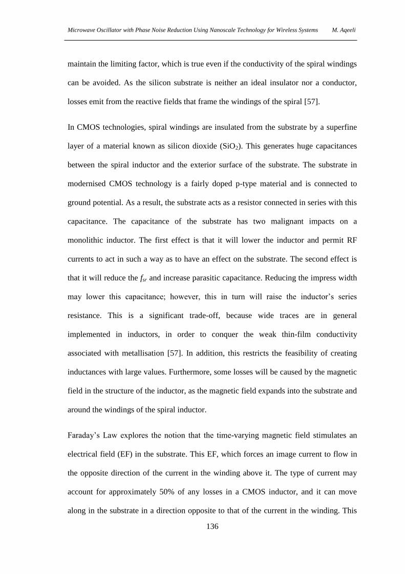
Microwave Oscillator with Phase Noise Reduction Using Nanoscale Technology for Wireless Systems M. Aqeeli
136
maintain the limiting factor, which is true even if the conductivity of the spiral windings
can be avoided. As the silicon substrate is neither an ideal insulator nor a conductor,
losses emit from the reactive fields that frame the windings of the spiral [57].
In CMOS technologies, spiral windings are insulated from the substrate by a superfine
layer of a material known as silicon dioxide (SiO2). This generates huge capacitances
between the spiral inductor and the exterior surface of the substrate. The substrate in
modernised CMOS technology is a fairly doped p-type material and is connected to
ground potential. As a result, the substrate acts as a resistor connected in series with this
capacitance. The capacitance of the substrate has two malignant impacts on a
monolithic inductor. The first effect is that it will lower the inductor and permit RF
currents to act in such a way as to have an effect on the substrate. The second effect is
that it will reduce the fsr and increase parasitic capacitance. Reducing the impress width
may lower this capacitance; however, this in turn will raise the inductor’s series
resistance. This is a significant trade-off, because wide traces are in general
implemented in inductors, in order to conquer the weak thin-film conductivity
associated with metallisation [57]. In addition, this restricts the feasibility of creating
inductances with large values. Furthermore, some losses will be caused by the magnetic
field in the structure of the inductor, as the magnetic field expands into the substrate and
around the windings of the spiral inductor.
Faraday’s Law explores the notion that the time-varying magnetic field stimulates an
electrical field (EF) in the substrate. This EF, which forces an image current to flow in
the opposite direction of the current in the winding above it. The type of current may
account for approximately 50% of any losses in a CMOS inductor, and it can move
along in the substrate in a direction opposite to that of the current in the winding. This

Microwave Oscillator with Phase Noise Reduction Using Nanoscale Technology for Wireless Systems M. Aqeeli
137
impact may also be assumed to be in the form of a parasitic transformer. Moreover,
large inductors’ magnetic fields infiltrate deeper into the substrate, and, as a result,
suffer from higher losses. This effect is in opposition to the target of limiting series
resistance, which includes wide spiral traces. Implementing high-resistivity Si substrates
[10], to etch away the substrate beneath the inductor, has an advantage of decreasing the
impact of the substrate. The influence of the magnetic field means that it will not only
infiltrate into the substrate, but it will also penetrate into the other windings of the coil,
and moreover it will promote further loss. The eddy current produced in the heart of a
winding will motivate the inner turns of the inductor to contribute a good deal more loss
to the inductor, though they will have a minimal influence on the actual inductor [57].
3.10.5: Inductor circuit models
A monolithic inductor circuit model on a low-resistivity substrate comprises circuit
parameters that model the loss mechanisms. It also models inductors on low resistivity
silicon substrates in a fairly accurate way, because it contains the impact of the
magnetic eddy currents. This model represents magnetic substrate loss as a perfect
transformer connected to a resistor, Rm. Generally, the inductance value of a monolithic
inductor L is calculated by simulated S-parameters or by converting the s-parameter into
Y-parameters. Then, the Y parameters are implemented to extirpate the values of Q and
L. If one side of the inductor is grounded, then L is often defined by the following
equation:
111
2
YL lm
f
(3.26)
Microwave Oscillator with Phase Noise Reduction Using Nanoscale Technology for Wireless Systems M. Aqeeli
138
When the inductor is implemented differentially, L is often defined [59] as follows:
121
2
YL lm
f
(3.27)
The difference between the two definitions can be explored with the help of the
equivalent π model of the two-port network, as shown in Figure 3.21, where the Y
parameters are admittances. For a symmetric network, Y11 = Y22, while for a passive
network, Y12 =Y21. To define the inductance value L and the Q factor, the π-model has to
be minimised to a single element so that the inductor will be allocated in series or in
parallel with resistance. Selecting the condition of a simple series element R+jX, then:
2
XL
f (3.28)
and
XQ
R (3.29)
Port 1 Port 2
11 12Y Y22 12Y Y
12Y
Figure 3.21 The π- equivalent circuit for a two-port network

Microwave Oscillator with Phase Noise Reduction Using Nanoscale Technology for Wireless Systems M. Aqeeli
139
Two methods are available in order to reduce the π-circuit to the series element R+jX, as
depicted in Figure 3.22.
Port 1Port 1
Port 2
ZinZin
(a) (b)
Figure 3.22 Two methods for reducing the π-network:
(a) single-ended and (b) differential configurations
When port two of the π-circuit is connected to the ground, the Y22+Y12 element is
bypassed, and the circuit looking into port one decreases to the admittance Y11
connected to the ground, since admittances are added in parallel and Y12 is removed
[57]. Converting admittance to impedance, R+jX becomes [12]:
11
1R jX
Y (3.30)
If this assumption is valid, L is defined using (4), and:
11
11
(1 )
Re(1 )
lm YQ
Y (3.31)
This method is applicable when the inductor is going to be implemented in a circuit
where one terminal of the inductor is grounded. Overwhelmingly, this is the situation in

Microwave Oscillator with Phase Noise Reduction Using Nanoscale Technology for Wireless Systems M. Aqeeli
140
many RF circuits, especially in mixers and low-noise amplifiers (LNAs), where
inductors are implemented for degeneration or loading. This method is synonymous
with taking the measurements of a one-port S-parameter with one terminal of the
grounded inductor and transforming the measured reflection coefficient into input
impedance. The series impedance is calculated as:
10
1
1
1inR jX Z Z
(3.32)
where
1 11S (3.33)
When an inductor that is going be used in a differential configuration means that neither
port is at AC ground potential, a different approach is required. Floating impedance,
R+jX, seen between port one and port two of the π-network, is [12]:
11 22 12
2
12 11 12 22 12 11 22 12
21 1 1 Y Y YR jX
Y Y Y Y Y Y Y Y
(3.34)
Equation 11 shows the impedance calculation and is referred to as ‘floating’ because it
disregards the connection to the ground in the equivalent circuit. Inductors connected
using these techniques are labelled ‘differential’ or ‘floating’. In this manner, the shunt
parameters Y11+Y12 and Y22+Y12 of the π-network will be parasitic capacitances and are
often ignored. This is especially true in technologies implementing semi-insulating
substrates, in which case Q is calculated as follows:

Microwave Oscillator with Phase Noise Reduction Using Nanoscale Technology for Wireless Systems M. Aqeeli
141
12
12
(1 )
Re(1 )
lm YQ
Y (3.35)
In standard CMOS technology, parameters Y11+Y12 and Y22+Y12 are not negligible.
Therefore, in order to calculate L and Q accurately, equation (3.34) can be used in
conjunction with (3.28) and (3.29).
3.11: Chapter summary
In this chapter‚ the implementation of wideband VCOs at the circuit level are described
in detail. Wideband tuning is designed with discrete and continuous tuning control
mechanisms to minimize VCO tuning sensitivity‚ and as a result reduce phase noise due
to tuning control line. The discrete tuning is designed with capacitance switching.
Differential structures are preferable for better common mode noise rejection and lower
switch resistance. In addition to that, active circuit design techniques are also explained.
The choices of a certain active circuit topology depend on the design requirements. The
use of pMOS transistors will lead to lower flicker noise. On the other hand, nMOS
transistors occupy a much smaller area, Hence, less parasitic capacitance affecting the
RF nodes of the VCO. Integrated inductors and varactors are also described.
Microwave Oscillator with Phase Noise Reduction Using Nanoscale Technology for Wireless Systems M. Aqeeli
142
CMOS Transistors Chapter 4:
4.1: Material properties
Silicon is the key material implemented in microelectronics technology. It is chemically
associated with other elements to obtain solid state devices, or what are typically known
as ‘integrated circuits’ [60]. The materials polysilicon, silicon dioxide and silicon nitride
are the most significant compounds used in microelectronics. Important elements such
as power dissipation and packaging require the use of several other inorganic and
organic elements. This section will consider the technological and physical properties
only of those compounds which are used significantly and specifically in ICs
technology.
4.1.1: Silicon
Monocrystalline silicon (MS) is the substrate on which ICs is constructed for
microelectronics. MS is composed of wafers or thin slices ranging from 300-1000µm in
size. Its physical properties are summarised in Table 4-1.
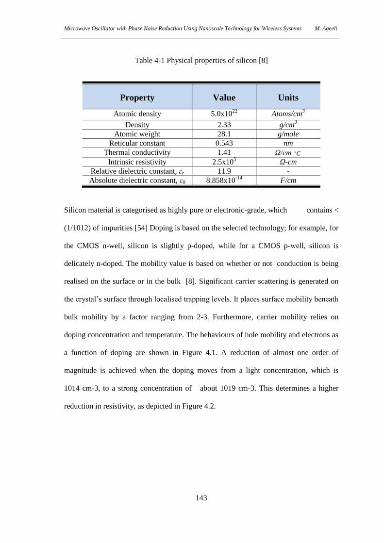
Microwave Oscillator with Phase Noise Reduction Using Nanoscale Technology for Wireless Systems M. Aqeeli
143
Table 4-1 Physical properties of silicon [8]
Property Value Units
Atomic density 5.0x10²²
Atoms/cm3
Density 2.33 g/cm3
Atomic weight 28.1 g/mole
Reticular constant 0.543 nm
Thermal conductivity 1.41 Ω/cm oC
Intrinsic resistivity 2.5x10⁵ Ω-cm
Relative dielectric constant, εr 11.9 -
Absolute dielectric constant, ε0 8.858x10⁻¹⁴
F/cm
Silicon material is categorised as highly pure or electronic-grade, which contains <
(1/1012) of impurities [54] Doping is based on the selected technology; for example, for
the CMOS n-well, silicon is slightly p-doped, while for a CMOS p-well, silicon is
delicately n-doped. The mobility value is based on whether or not conduction is being
realised on the surface or in the bulk [8]. Significant carrier scattering is generated on
the crystal’s surface through localised trapping levels. It places surface mobility beneath
bulk mobility by a factor ranging from 2-3. Furthermore, carrier mobility relies on
doping concentration and temperature. The behaviours of hole mobility and electrons as
a function of doping are shown in Figure 4.1. A reduction of almost one order of
magnitude is achieved when the doping moves from a light concentration, which is
1014 cm-3, to a strong concentration of about 1019 cm-3. This determines a higher
reduction in resistivity, as depicted in Figure 4.2.

Microwave Oscillator with Phase Noise Reduction Using Nanoscale Technology for Wireless Systems M. Aqeeli
144
1E14 1E15 1E16 1E17 1E18 1E19
100
1000
10000
Mo
bili
ty (
cm
2/V
.sec)
Doping Concentration (cm-3)
Electrons
Holes
Figure 4.1 Mobility of electrons and holes in bulk silicon at T=300 [7]
1E14 1E15 1E16 1E17 1E18 1E19 1E20 1E21
1E-4
1E-3
0.01
0.1
1
10
100
Resis
tivity (
Ohm
-cm
)
Doping Concentration (cm-3)
n-typep-type
Figure 4.2 Resistivity of bulk silicon versus doping concentration [7]
The properties and the specifications of homogeneous silicon were discussed briefly in
the section above. Nevertheless, an integrated circuit does not use homogeneous
materials, thereby permitting several structures to be implemented which guarantee the
Microwave Oscillator with Phase Noise Reduction Using Nanoscale Technology for Wireless Systems M. Aqeeli
145
adequate alteration of doping in dedicated regions. Several doping concentrations are
obtained by selective masking correlated with thermal diffusion and ion implantation.
These two steps result in great modifications in doping and will convert it from a
fraction into thin layers of about a few microns close to the surface. Doping appears like
an error function or a Gaussian. The functions of doped layers are used to make
resistors and to create active devices which are nominated as sources and drains for
CMOS transistors. To speed up the performance of the transistor, the source and the
drain must have the lowest possible resistance. In contradiction, to create a resistor, the
resistivity features of the diffused layers must be exploited. In order to make a resistor, a
diffused layer is used and the engineer must evaluate the achieved resistance value.
Silicon dioxide 4.1.1.1:
Microelectronics technology uses silicon dioxide for two reasons. The first is to make
active devices and the second is to ensure insulation, because of its features as an
excellent insulator. The thickness of the silicon dioxide used depends on the steps of the
specific fabrication. A very important parameter of the physical properties of the
silicon dioxide to consider is dielectric strength, which spans from 2 to 8 MV per
centimetre, with the higher value pertaining to monocrystalline silicon oxide and the
lower value to polysilicon oxide. With this amount of dielectric strength, the possibility
of supporting 6 V to 24 V in a modern technology 30 nm gate oxide thickness is very
high.
Microwave Oscillator with Phase Noise Reduction Using Nanoscale Technology for Wireless Systems M. Aqeeli
146
Polysilicon 4.1.1.2:
Polysilicon is an increasingly important element in modern technology, and it has been
used to create MOS transistor gates, for short interconnections, and most importantly to
make capacitor plates. Conductivity tolerance is obtained through doping the
polysilicon at approximately 1020-1021 atoms/cm3. Consequently, the polysilicon
layer’s sheet resistance will be between 20-40 ohm/seq. It should be noted that this
small value is not sufficient for many applications, because it might produce a noisy
operation. A primary concern of high resistive gates is that they will limit the speed of
the transistor. In the history of development, sheet resistance has improved by
employing sandwiched layers, which have remarkable sheet resistance between 1 and
5ohm/seq [8].
4.2: CMOS Technology
Frank Wanlass invented the CMOS circuit design in 1963 [61]. Promoting the idea of a
circuit that could be made with discrete complementary MOS devices, an nMOS and a
pMOS transistor were novel at the time, especially given the immaturity of MOS
technology and the growing implementation of the bipolar junction transistor (BJT) as a
replacement for the vacuum tube.
MOS transistors are the most sophisticated and important manufactured devices in the
history of mankind. Nowadays, more than 95% of integrated circuits are fabricated in
CMOS. In 1968, a team supervised by Albert Medwin [62] created the first CMOS
integrated circuits. At first, CMOS circuits were slower and weaker alternatives to BJT
logic circuits using transistor-transistor logic (TTL) digital logic. During the 1970s,
Microwave Oscillator with Phase Noise Reduction Using Nanoscale Technology for Wireless Systems M. Aqeeli
147
watch factories used CMOS technology for computing processor development, which
led ultimately to the revolution of the personal computer industry in the 1980s and the
launch of internet technology in the 1990s. For the present and prospective future,
CMOS will continue be the dominant technology for fabricating integrated circuits.
This is true for various reasons. The first reason is that CMOS integrated circuits can be
housed in a very small area. Secondly, they can achieve very high operating speeds and
dissipate relatively low power. Thirdly, and very importantly, CMOS circuits are
possibly being fabricated with very few defects. Finally, fabrication costs remain low by
reducing device scaling through the continuous development of new generations of
technology.
At first, CMOS was utilised particularly for digital design, but the unending push to
increase functionality and minimise the costs of ICs has resulted in the technology being
used for mixed-signal chips that combine a digital signal with analogue circuits,
analogue/digital and analogue-only design. Both n-channel and p-channel transistors
can be employed on a chip using integrated CMOS technology [63]. For a p-doped
substrate, n-channel transistors are positioned directly on the substrate, while a well is
mandatory for p-channel devices. With regard to the n-type substrate, p-channel
transistors are fabricated in the substrate and n-channel transistors are positioned inside
the p-well. Twin wells are used in advanced technologies, in order to fabricate both
transistor categories inside wells, without paying attention to substrate doping to
optimise electrical behaviour.

Microwave Oscillator with Phase Noise Reduction Using Nanoscale Technology for Wireless Systems M. Aqeeli
148
4.2.1: The characterisation of the I-V curve
Explaining the operation of the MOSFET transistor helps to focus on the structure of
the transistor, and to do this it is important to study the MOSFET transistor current
versus, I-V curves. Looking at the structure of the nMOS transistor depicted in Figure
4.3, it can be seen a P-type waver, gate electrode, source and drain diffusion, using an n-
channel and p-diffusion, in order to make contact with the P-type substrate. In reality, a
third dimension extends the gate electrode and similarly the source, the drain and the
diffusion region. The region under the gate electrode is where the channel that is going
to be formed, and the distance between them, is the channel length, L. The channel
width is the other dimension, namely the width of the transistor.
Gate
P-type
substrate
Depletion region
DrainSource
GS ThV V
N+N+P+
Figure 4.3 nMOS transistor on a P-type silicon waver [66]
Assume that the source, drain and the substrate are connected to the ground. If a voltage
is applied to the gate, VGS , then an electrical field will be created beneath the gate; it is
also known that the p-region has holes. Therefore, these holes will be repelled and
pushed downwards by this electrical field, and electrons will be attracted to the surface
when the operation starts to happen. When it reaches a critical voltage, known as the
‘threshold, VTH, a sufficiently strong enough electric field will form to invert the p-type
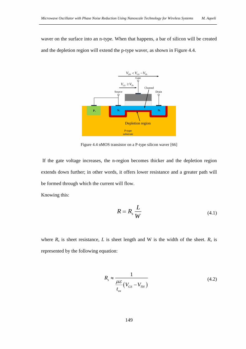
Microwave Oscillator with Phase Noise Reduction Using Nanoscale Technology for Wireless Systems M. Aqeeli
149
waver on the surface into an n-type. When that happens, a bar of silicon will be created
and the depletion region will extend the p-type waver, as shown in Figure 4.4.
Gate
P-type
substrate
Depletion region
DrainSource
GS ThV VChannel
DS GS ThV V V
N+N+P+
Figure 4.4 nMOS transistor on a P-type silicon waver [66]
If the gate voltage increases, the n-region becomes thicker and the depletion region
extends down further; in other words, it offers lower resistance and a greater path will
be formed through which the current will flow.
Knowing this:
s
LR R
W (4.1)
where Rs is sheet resistance, L is sheet length and W is the width of the sheet. Rs is
represented by the following equation:
1s
GS TH
ox
R
V Vt
(4.2)

Microwave Oscillator with Phase Noise Reduction Using Nanoscale Technology for Wireless Systems M. Aqeeli
150
where µ is channel mobility, ε is the permittivity of the region under the gate electrode,
tox is the thickness of the region under the gate electrode, VGS is the gate-to-source
voltage and VTH is the threshold voltage. Note that when the gate-to-source voltage
increases, the dominator becomes larger, and the channel between the drain and the
source will be driven down and sheet resistance will be lower. The main question relates
to what will happen if the drain and the source voltage are not equal? From a fabrication
point of view, it can be said the drain and the source are interchangeable, and what
distinguishes them is the voltage level; for an nMOS transistor, the voltage of the source
is usually low such as ground level. Connect a controlled voltage source to the drain
and similarly another controlled voltage source to the gate. Then, by setting the drain
voltage to zero and increasing VGS until it overcomes VTH, the n-type will start to form
between the drain and the source [63].
If the drain voltage increases, the electrical field will become weaker and the channel is
now not driven down and resistance increases, as shown in Figure 4.5.
Gate
P-type
substrate
Pinched-off channel
DrainSource
GS ThV V
DS GS ThV V V
N+N+P+
Figure 4.5 nMOS transistor on a P-type silicon waver
I-V characteristics can be determined by differentiating between three regions of
operation. The first one is weak inversion, whose gate voltage is VG < VTH. Second is
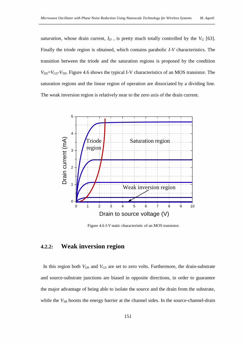
Microwave Oscillator with Phase Noise Reduction Using Nanoscale Technology for Wireless Systems M. Aqeeli
151
saturation, whose drain current, ID , is pretty much totally controlled by the VG [63].
Finally the triode region is obtained, which contains parabolic I-V characteristics. The
transition between the triode and the saturation regions is proposed by the condition
VDS=VGS-VTH. Figure 4.6 shows the typical I-V characteristics of an MOS transistor. The
saturation regions and the linear region of operation are dissociated by a dividing line.
The weak inversion region is relatively near to the zero axis of the drain current.
0 1 2 3 4 5 6 7 8 9 10
0
1
2
3
4
5
Dra
in c
urr
en
t (m
A)
Drain to source voltage (V)
Saturation regionTriode
region
Weak inversion region
Figure 4.6 I-V static characteristic of an MOS transistor.
4.2.2: Weak inversion region
In this region both VDS and VGS are set to zero volts. Furthermore, the drain-substrate
and source-substrate junctions are biased in opposite directions, in order to guarantee
the major advantage of being able to isolate the source and the drain from the substrate,
while the VSB boosts the energy barrier at the channel sides. In the source-channel-drain

Microwave Oscillator with Phase Noise Reduction Using Nanoscale Technology for Wireless Systems M. Aqeeli
152
structure, two p-n diodes are recognised. When voltage is applied between the source
and the drain, it will fall approximately across the inversely biased diode, and the
current of the transistor will be specified by its reverse saturation current, Isat. This
current relies exponentially on the height of the energy barrier. As the VGS increases, a
fraction of it, for instance ((n-1)/n), spreads across the gate oxide, while a fraction of 1/n
detracts the barrier.
The increase in the reverse Isat can be calculated as follows [64]:
G Bqv nkt qv nkt
sat DOI I e e
(4.3)
Taking into account the slight dependence on the VDS voltage, which acts as a reverse
biasing voltage, the drain current ID is calculated as [64]:
[1 ]G Bqv nkT qv nkT qvDS nkT
D DOI I e e e (4.4)
In a weak inversion, result indicates that, the IV MOS characteristic alters exponentially
with changes to the control voltage, while a MOS transistor (sub-threshold) performs
similar to the bipolar transistor in the weak inversion region [64]. On the other hand,
voltage remains the electrical source that controls the operation of the device.

Microwave Oscillator with Phase Noise Reduction Using Nanoscale Technology for Wireless Systems M. Aqeeli
153
4.2.3: Triode region
When VGS > VTh, the oxide-silicon will be linked to strong inversion, which starts when
VGS =VTh. When applying a larger voltage, the surplus part will lead to an build-up of
mobile charges at the oxide-semiconductor interface, subsequently forming the
inversion layer. The charge per unity area, Qinv, for a generic position x, is calculated by
[64]:
( ) ( ) ( )inv OX GS ThQ x C V V x V x (4.5)
which relies on two parameters; the first one is the resulting threshold voltage. And the
second one is the variation the drop voltage, V(x), along the channel. To calculate
resistance across an infinitesimal element, dx, of the channel, the following equation is
implemented [64]:
( )inv
dx dxdR
A Q x W (4.6)
where W is the width of the transistor and µ is carrier mobility. The subsidence voltage
is calculated as follows [64]:
[ ( ) ( )]
DD
OX GS Th
I dxdV I dR
C V V x V x W
(4.7)
Along the channel, VTH changes due to the body effect, as stated by the following
equation [64]:

Microwave Oscillator with Phase Noise Reduction Using Nanoscale Technology for Wireless Systems M. Aqeeli
154
,0 2 ( ) 2 Th Th SB F FV V V V x (4.8)
Substituting equation (4.6) in equation (4.7), the drain current can be calculated as
follows [64]:
3 2 3 22
,0
1 2( 2 ) [ 2 2 ]
2 3D OX GS Th F DS DS SB F SB F
WI C V V V V V V
L
(4.9)
Neglecting the impact of equation (4.8), to calculate for differences in the condition of
the Vth along the channel, therefore, equation (4.9) can be simplified as follows:
21( )
2D OX GS Th DS DS
WI C V V V V
L
(4.10)
It can be observed from equations (4.9) and (4.10) that both consist of the term
OXC W L , thus ID is larger, with electrons acting as mobile carriers for thinner
gate oxides. This is true because their mobility is greater than that of the holes.
Furthermore, the ID is proportional to the (W/L) ratio of the gate. In addition, equation
(4.10) illustrates a parabola, with its maximum obtained at:
GS Th DSV V V (4.11)
Microwave Oscillator with Phase Noise Reduction Using Nanoscale Technology for Wireless Systems M. Aqeeli
155
It can be observed that when the above condition is implemented in equation (4.5), the
charge in the inverted layer at the drain end (x=L; V(L)=VDS) goes to zero page. Since
the inversion layer is irreversible, any VDS voltage larger than the one given by equation
(4.11) will result in an unrealistic situation. Equation (4.11) establishes the limits of the
triode region and realises the applicability limit of the above formulation. It must be
noted that for a very small drain to source voltage, VDS (VGS-VTh>>VDS), the I-V curve
approximates a straight line with a slope proportional to VGS [64].
4.2.4: Saturation region
The transistor departs the linear region and moves to the saturation region when voltage
at the VG gate is greater than the threshold Vth and when VDS exceeds the saturation
voltage, Vsat. This is defined as follows:
DS GS ThV V V (4.12)
In this region, the inversion layer disappears inside the channel, and part of the channel,
∆L, becomes depleted, as depicted in Figure 4.7. Consequently, as the drain voltage
increases, the channel pinches off more, as shown in Figure 4.7. As a result, the
effective channel length, Leff , will decrease and the electrons will be attracted to the
drain region, so more or less will have a constant current source, which can be described
by the following equation [64]:
2
2D GS TH
ox eff
WI V V
t L
(4.13)

Microwave Oscillator with Phase Noise Reduction Using Nanoscale Technology for Wireless Systems M. Aqeeli
156
It can be noted from equation 4.13 that as the drain current increases, the effective
channel length decreases.
Gate
P-type
substrate
DrainSource
GS ThV VChannel
DS GS ThV V V
N+N+P+
Pinched-off channel
effL L
Figure 4.7 nMOS transistor in the saturation region [66]
The voltage across the depleted part is:
DS satV V V (4.14)
Width ∆L can be approximated by:
2( )DS sat
A
L V VqN
(4.15)
The current flowing in the transistor can be estimated from equations (4.10) and (4.12)
as follows [64]:
2 21 1( )
2 2D OX GS Th OX DS
W WI C V V C V
L L L L
(4.16)
where (L/L-∆L) is the correcting factor for the reduction of the channel length.

Microwave Oscillator with Phase Noise Reduction Using Nanoscale Technology for Wireless Systems M. Aqeeli
157
From equation (4.15), the correcting factor can be written as:
2
1
21 ( )DS sat
A
L
L LV V
qN L
2
21 ( ) 1DS sat DS
A
V V VqN L
(4.17)
The new parameter, which is defined as , represents the channel modulation
parameter. ( )DS satV V is replaced with VDS , while the other square root is included in
parameter . From (4.17), channel length modulation will cause a linear increase in the
ID , which is after the approximation and can be seen as being proportional to VDS. An
empirical expression for is as follows:
710
.AN L (4.18)
where NA is the doping concentration, in cm-3, and the length, L, is measured in
microns. The ID in the saturation region can be obtained by combining equation (4.16)
with equation (4.17) [64]:
21( ) (1 )
2D OX GS Th DS
WI C V V V
L
(4.19)
It can be noted from the I-V characteristics expressed in equation (4.10) that a zero
slope in the ID-VDS plane exists on the boundary between the triode region and the

Microwave Oscillator with Phase Noise Reduction Using Nanoscale Technology for Wireless Systems M. Aqeeli
158
saturation region. On the other hand, the slope calculated using equation (4.19) is .
The parameter µCox is frequently demonstrated by the symbols kn or kp that are
nominated as the process transconductance, namely their values based on the type of
channel carrier and the implemented technology. For developed CMOS technologies,
the following figures can be used: µn =460cm2 / Vsec and µp=148cm
2/Vsec, tox=12nm;
consequently, for transistors’ n- and p-channels, this technology leads respectively to
the following [65]:
2120 /n n OXk C A V (4.20)
239 /p p OXk C A V (4.21)
To conclude, it can be posited that the nMOS transistor has three modes of operation.
The first mode occurs when VGS < VTh, in which case the transistor is in either the cut-
off mode or the off mode. The second mode occurs when VGS < VTh,, i.e. when the
transistor turns on. The third mode occurs when VGS > VTh,in the presence of a large VDS
value, in which case the transistor behaves as a current source in which the current flow
becomes independent of VDS. On the other hand, if the value of VDS is small, then the
current flow in the transistor will be proportional to VDS and the transistor will behave as
a linear resistor. With regard to pMOS transistors, these operate in the opposite way.
The n-type body is connected to a high potential, so any junctions with the p-type drain
and the source are reverse-biased [66]. In the case, if the gate holds high potential, then
there will be no current between the drain and the source.
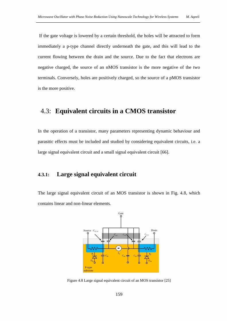
Microwave Oscillator with Phase Noise Reduction Using Nanoscale Technology for Wireless Systems M. Aqeeli
159
If the gate voltage is lowered by a certain threshold, the holes will be attracted to form
immediately a p-type channel directly underneath the gate, and this will lead to the
current flowing between the drain and the source. Due to the fact that electrons are
negative charged, the source of an nMOS transistor is the more negative of the two
terminals. Conversely, holes are positively charged, so the source of a pMOS transistor
is the more positive.
4.3: Equivalent circuits in a CMOS transistor
In the operation of a transistor, many parameters representing dynamic behaviour and
parasitic effects must be included and studied by considering equivalent circuits, i.e. a
large signal equivalent circuit and a small signal equivalent circuit [66].
4.3.1: Large signal equivalent circuit
The large signal equivalent circuit of an MOS transistor is shown in Fig. 4.8, which
contains linear and non-linear elements.
Gate
P-type
substrate
DrainSource ,GS ovC
GSC GDC ,GD ovC
BSD
BSC BGCBDC
DBD
DRDISR
Figure 4.8 Large signal equivalent circuit of an MOS transistor [25]

Microwave Oscillator with Phase Noise Reduction Using Nanoscale Technology for Wireless Systems M. Aqeeli
160
Resistors Rs and Rd depicted in Figure 4.8, in contact with the ends of the channel, are
described as resistive paths from the source and the drain values and depend on the
aspect ratio of the contact regions and on the particular resistance of the diffused layers,
with values typically between 10 and 50Ω. With respect to the two diodes, DBS, DBD,
and their parasitic capacitances, it can be said that they insulate the source and the drain
from the substrate through reversely biased p-n junctions. An important issue in circuit
performance is leakage current, because in reverse biased conditions this is controlled
by what is known as the ‘effect of generation recombination’, IGR, which is expressed
by [64]:
02
i j
GR
qn xI A
(4.22)
where A is the area of the junction, q is the electron charge, ni is the intrinsic carrier
concentration, xj is the width of the depletion region and 0 is the mean lifetime for
minority carriers. It should be noted that the IGR is proportional to the depletion width.
Consequently, as reverse biasing increases, the current increases. In addition, IGR is
proportional to ni, thereby making it exponentially dependent on temperature – at room
temperature, the value of IGR ranges from 10-7
to 10-16
A/µm2.
CBS and CBD, depicted in Figure 4.8, show the junction capacitance of the diodes. Step
junctions are proportional to the area of the junction and inversely proportional to the
square root of the reverse biasing. Thus, the drain and the source contact areas must be
reduced whilst ensuring an acceptable value for Rs and Rd. The capacitive behaviour of
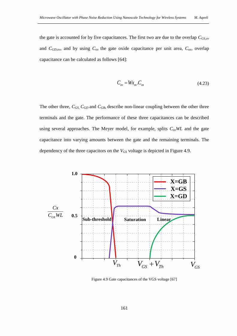
Microwave Oscillator with Phase Noise Reduction Using Nanoscale Technology for Wireless Systems M. Aqeeli
161
the gate is accounted for by five capacitances. The first two are due to the overlap CGS,ov
and CGD,ov, and by using Cox the gate oxide capacitance per unit area, Cox, overlap
capacitance can be calculated as follows [64]:
.ov ov oxC Wx C (4.23)
The other three, CGS, CGD and CGB, describe non-linear coupling between the other three
terminals and the gate. The performance of these three capacitances can be described
using several approaches. The Meyer model, for example, splits CoxWL and the gate
capacitance into varying amounts between the gate and the remaining terminals. The
dependency of the three capacitors on the VGS voltage is depicted in Figure 4.9.
Saturation
ThVGSVGS ThV V
LinearSub-threshold
X=GB
X=GS
X=GD
0
0.5OX
Cx
C WL
1.0
Figure 4.9 Gate capacitances of the VGS voltage [67]

Microwave Oscillator with Phase Noise Reduction Using Nanoscale Technology for Wireless Systems M. Aqeeli
162
It can be said that coupling with the source and the drain in the sub-threshold region is
very weak, because the conductive channel has not been created. Consequently, CGB is
considerable capacitance. On the contrary, in the saturation and linear region, the
conductive channel generates equivalent shielding for the substrate; therefore, CGB turns
out to be negligible. With regard to the linear region, the channel is equal to resistance
located directly underneath the gate.
4.3.2: Small signal equivalent circuit
The small signal equivalent circuit is depicted in Figure 4.10. The id source produces
three terms vgs, vds and vbs, which are proportional to the small signal voltages and thus
[64]:
( , , ) D D Dd gs ds bs gs ds bs
GS DS BS
I I Ii v v v v v v
V V V
(4.24)
d m gs ds ds mb bsi g v g v g v (4.25)
mb bsg vm gsg v
gdC
gbCgsC
dbCsbC
di
gsv
bsv
gate
source
drain
bulk
+
--
+
0r
Figure 4.10 Small signal equivalent circuit of an nMOS transistor [67]

Microwave Oscillator with Phase Noise Reduction Using Nanoscale Technology for Wireless Systems M. Aqeeli
163
Equations (4.24) and (4.25) define transconductance gm, output conductance gds and the
substrate transconductance gmb, and they are calculated in three regions of operation.
Starting with the weak inversion region [64]:
D
m mb
Ig g
kTnq
(4.26)
ds wi Dg I (4.27)
In the linear region:
m OX DS
Wg C V
L
(4.28)
[ ]ds OX GS Th DS
Wg C V V V
L
(4.29)
In the saturation region,
2( )
( )
Dm OX GS Th OX D
GS Th
IW Wg C V V C I
L V V L
(4.30)
ds Dg I (4.31)
where the dimension is V-1
. Analogue applications usually use the saturation region.
It can be noted from equation (4.30) that transconductance is inversely proportional to
the overdrive voltage GS ThV V , directly proportional to the current, and
transconductance is proportional to the square root of the transistor’s aspect ratio (W/L)
and to the square root of the drain current. Figure 4.11 shows the plot of ID versus gm/ID.

Microwave Oscillator with Phase Noise Reduction Using Nanoscale Technology for Wireless Systems M. Aqeeli
164
When ID turns small, the transistor moves into the region of the weak inversion, and
transconductance, as mentioned in equation (4.26), corresponds to the ID. The transition
between the weak inversion and the saturation regions is relatively consistent. In fact, it
is hard to find the transition point between these two regions when implementing the
equations describing the I-V relationship [64].
Drain current (A)
()
mD
gI
IV
W/L=1000
W/L=100
W/L=10
W/L=1
10
0.001
0.01
0.1
1
10n 100n 1µ 10µ 100µ
Figure 4.11 Transconductance versus the drain current in a sub-threshold and saturation [64]
Suppose that transconductance gm never shows discontinuity; as a consequence, the
transition between the two regions will take place at current DI , for which [64]:
D
OX D
I WC I
LkTnq
(4.32)
solve for ID:

Microwave Oscillator with Phase Noise Reduction Using Nanoscale Technology for Wireless Systems M. Aqeeli
165
2
2D OX
WkTI n Cq L
(4.33)
In CMOS technology at room temperature, with n=1.5 and the area of the transistor
(W/L=1), the transition point is achieved at approximately 328 nA and 115 nA for
nMOS and pMOS transistors, respectively.
4.4: Cadence virtuoso analogue design environment
Designing integrated circuits requires very complicated operations. Consequently, it is
recommended to use sophisticated devices that can be easily handled with computer
simulation software. In this thesis, the Cadence Virtuoso Analogue Design Environment
(CVADE) is implemented, which is the advanced design and simulation environment
for the Virtuoso platform [67]. This revolutionary software was designed and
constructed to help researchers create reliable and solid designs. Cadence certainly
plays a fundamental factor in the creation of today’s integrated circuits and authorises
global electronic design innovations. Researchers across the globe use Cadence
software as well as methodologies to design and justify advanced semiconductors,
computer systems and consumer electronics. It is the market-leading design system in
global electronic-design innovation, and UMC is a leading global semiconductor
manufacturer which recently announced the existence of design kits for the UMC 130-
nanometer foundry employed in this research work through the latest CVADE design
platform (IC 6.1) release which allows for phase noise variations in VCOs. Researchers
use UMC’s logic/mixed-mode 130-nanometer logic/mixed mode RF 130-nanometer
low-leakage (LL) process and standard performance (SP) process [68]. Detailed
Microwave Oscillator with Phase Noise Reduction Using Nanoscale Technology for Wireless Systems M. Aqeeli
166
parameters for the UMC 130nm transistors standard performance enhancement 1.2 V
using Cadence Virtouso is shown in Appendix B.
The CVADE technology helps to accelerate the silicon circuit design of analogue, RF
and mixed-signal devices. It was noted during this project that the availability of the
130-nm design kits supports all designs reported in this thesis and more quickly realises
the performance of the circuits, phase noise and power consumption. Furthermore, the
developed Virtuoso platform with UMC’s kits [11] will accelerate development time for
researchers, engineers and scientists, to help them meet their targets accurately.
Cadence Virtuoso solutions and UMC’s nanoscale technology support designers in the
rapidly developing IC world. These technologies present advanced processes for the
unmatched integration of mixed-signal and digital designs. The kit used in this work
allows for leveraging features of both the UMC 130-nanometer process and the
CVADE platform in reported and upcoming designs, to meet the requirements of high
performance. UMC is a leading global and advanced developed semiconductor foundry
that manufactures advanced designs for applications covering a considerable area of IC
manufacturing. Its strategy is based on the beneficial quality of advanced technologies,
which involve proven nanoscale technology and mixed signal/RFCMOS. UMC’s
production is corroborative, through 10-wafer manufacturing. Wireless applications
designers gain a competitive advantage by implementing CVADE in conjunction with
UMC’s RFCMOS process. With regard to back annotation verification, Cadence QRC
Extraction supplies an accurate methodology to predict performance in critical design
circuits, such as high performance, low phase noise and a wideband LC tank VCO. In
addition, the extraction that covers RLCK can be used to predict greater frequency
accuracy and how the circuit will perform in silicon [11].

Microwave Oscillator with Phase Noise Reduction Using Nanoscale Technology for Wireless Systems M. Aqeeli
167
4.5: CMOS resistors and capacitors
An analogue ICs device is made from active and passive components. This section
explores the properties, major characteristics and limits of some of the most important
integrated passive components, such as resistors and capacitors. In monolithic form, the
operation of passive elements is dissimilar to that of the corresponding discrete or ideal
versions.
4.5.1: Integrated resistors
In integrated technology, resistors are fabricated on a thin resistive layer. The typical
structure consists of a long sheet of resistive material connected to metal terminals by
two ohmic contacts, as shown in Figure 4.11.
Metal
WL
Figure 4.11 Integrated resistor in n-well
A reversely biased junction, or an oxide layer, is employed to insulate the body of the
resistance. Total resistance, R, is calculated by:
2 cont
LR R R
W (4.34)
where Rcont is resistance representing the contacts of the metal connection, ranging
between 10 and 50 Ohme. R is the sheet resistance. Resistant elements are obtained by
diffused layers, n+, p
+ and a well, or by polysilicon. Importantly, it is well known that
Microwave Oscillator with Phase Noise Reduction Using Nanoscale Technology for Wireless Systems M. Aqeeli
168
resistances range from a few tens of Ohms per square to a few kilo-ohms per square. As
a result, achieving resistor values up to a few kilo-ohms is realistic. On the other hand, it
would be impossible to reach ( 0.1-100) MΩ. Cross-sections of various n-well CMOS
technology CMOS integrated resistor structures are shown in Figures 4.12 (a) and (b).
Insulation is obtained by reversely biased junctions. A highly-doped diffusion is
implemented in both resistors; the first has a diffusion sitting inside the well and the
second one utilises a diffusion obtained directly on the substrate.
P-type
substrate
P+ N+N+
n-Well
(a)
n-type
substrate
N+
Diffusion
Metal
(b)
Figure 4.12 Cross-section of integrated resistances: (a) diffusion into a well (b) diffusion [1]
It can be noticed from Figure 4.12 that the n+ and p
+ layers touch the metal lines
directly. On the other hand, the slightly doped diffusion of the well has intermediate n+
diffusion. In order to confirm that the insulation of the resistance produces a capacitive
coupling between the substrate and the body of the resistor, a reversely biased diode is
employed. This parasitic capacitance will not cause any limitation to the frequency, but
it will be mandatory to interact with it, because the resistor might be affected by this

Microwave Oscillator with Phase Noise Reduction Using Nanoscale Technology for Wireless Systems M. Aqeeli
169
noise. Due to the fact that spur signals definitely influence the substrate through
parasitic coupling, this noise approaches the resistance and as result leads to poorer
performance. It is very important to mention that in mixed signal integrated circuits,
substrate noise is one of the most critical restrictions to resolution, and because
integrated resistors are completely sensitive devices, they need very careful protection
against substrate noise coupling. It can be said that placing resistors in the well will
provide some protection, because the well supplies some form of local shielding. The
basic structure of a well resistor is depicted in Figures 4.13 (a) and (b) with a p-type
substrate [1].
P-type
substrate
N+N+
n-Well
(a)
P-type
substrate
P+ N+N+
n-Well
(b)
Figure 4.13 Cross-section of integrated resistances: (a) well (b) pinched well [1]
Relatively speaking, the resistance of wells is fairly high. Nonetheless, in order to
increase the resistivity of layers, a complementary diffusion has to be placed above the
well, in order to reverse doping at the surface. Resistance is obtained with an entombed
layer; in this case, doping concentration will be greater than on the surface. Figure

Microwave Oscillator with Phase Noise Reduction Using Nanoscale Technology for Wireless Systems M. Aqeeli
170
4.13(b) shows the resulting structure, referred to as a ‘pinched well’. It can be said that
this resistance increases significantly from only a few kΩ to several kΩ. In addition, a
huge reduction in noise (1/f) in the lower frequency is obtained because conduction will
exist in the bulk of the material. Polysilicon material implementation offers a good way
to face the issue situation of shielding. Polysilicon can be employed to design resistors;
some typical structures are shown in Figures 4.14 and 4.15. Polysilicon is not in the
direct environment of the substrate, and so this will result in a weaker coupling in
comparison with diffusion. In addition, single or double shielding can be employed [1].
n-type
substrate
MetalPolysilicon
Figure 4.14 Cross-section of a polysilicon integrated resistance [1]
n-Well
MetalPolysilicon
N+
Figure 4.15 Cross-section of integrated resistances with well shielding [1]
4.5.2: Integrated resistor accuracy
This section focus on achievable relative accuracy and achievable absolute accuracy in
designing resistors using integrated technology. Assuming that the resistance of the strip
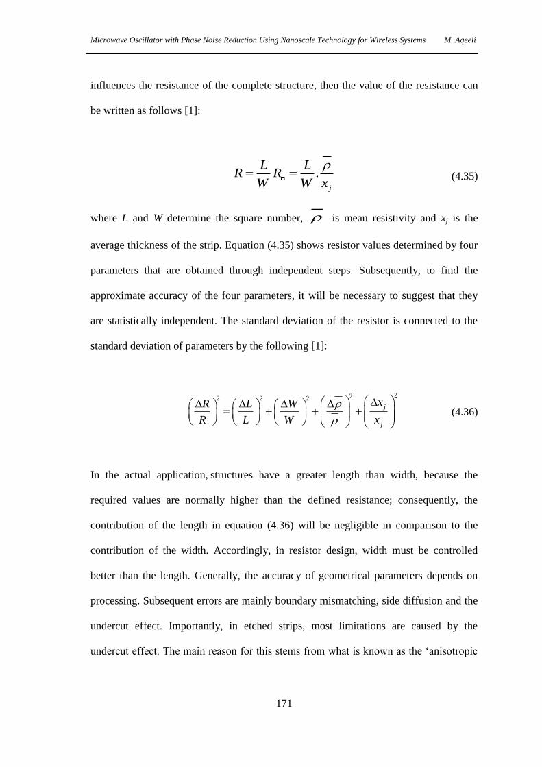
Microwave Oscillator with Phase Noise Reduction Using Nanoscale Technology for Wireless Systems M. Aqeeli
171
influences the resistance of the complete structure, then the value of the resistance can
be written as follows [1]:
.j
L LR R
W W x
(4.35)
where L and W determine the square number, is mean resistivity and xj is the
average thickness of the strip. Equation (4.35) shows resistor values determined by four
parameters that are obtained through independent steps. Subsequently, to find the
approximate accuracy of the four parameters, it will be necessary to suggest that they
are statistically independent. The standard deviation of the resistor is connected to the
standard deviation of parameters by the following [1]:
222 2 2
j
j
xR L W
R L W x
(4.36)
In the actual application, structures have a greater length than width, because the
required values are normally higher than the defined resistance; consequently, the
contribution of the length in equation (4.36) will be negligible in comparison to the
contribution of the width. Accordingly, in resistor design, width must be controlled
better than the length. Generally, the accuracy of geometrical parameters depends on
processing. Subsequent errors are mainly boundary mismatching, side diffusion and the
undercut effect. Importantly, in etched strips, most limitations are caused by the
undercut effect. The main reason for this stems from what is known as the ‘anisotropic

Microwave Oscillator with Phase Noise Reduction Using Nanoscale Technology for Wireless Systems M. Aqeeli
172
action’ of the etch, where the etching process is taken place further the required and the
erosion below the protection results, as depicted in Figure 4.16 (a).
The resulting pattern is lower than the designed one by a magnitude of ∆x, which
depends on the etching process and the implemented etched material. For polysilicon,
using moisten etching, ∆x ranges from 0.2µm to 0.4µm with a standard deviation of
0.04-0.08µm, while in ion etching, the undercut is usually tiny for the reactive example,
where ∆x is approximately 0.05µm with a standard deviation of 0.01µm.
Mask
More active Less active
Mask
∆X
(a) (b)
Figure 4.16 Undercut effect and its boundary dependence [1]
In addition, the boundary dependence of undercut etching is one of the major sources of
inaccuracy. As shown in Figure 4.16 (b), etching becomes active if the region that
needed to be taken off is extensive. Alternatively, if the strip to be taken off is narrow,
this will be less effective. As a result, the undercut on the strip conducts on the two
sides in dissimilar ways, due to differences between the boundaries. Therefore, if a
number of parallel closed strips need to be designed, such as in serpentine resistance,
elements which contain two terminals will undergo huge etching locating on the
external side. As a result, what will happen in the terminal elements is that a smaller
width will stimulate a huge resistor value and an error in this resistor value will occur.
This problem can be resolved by using dummy strips which do not have any electrical

Microwave Oscillator with Phase Noise Reduction Using Nanoscale Technology for Wireless Systems M. Aqeeli
173
function allocated around the structure. These dummy elements are employed to define
symmetrical geometry and to provide exactly the same undercut effect on both sides of
the etched strip. It can be concluded that temperature has a very big impact on the
resistivity of diffused layers and, as a result, on integrated resistors.
The temperature coefficient can be as large as 1%/°C, corresponding to a considerable
increase in the resistor’s magnitude for a minor change of temperature, which might
result in resistor mismatching. If a chip circuit includes a power device, the temperature
gradient will be determined by the dissipation of this device. Consequently, the average
temperature of the resistors might differ, as depicted in Figure 2.17 (a). In addition,
inside the chip, temperature varies in line with power dissipation. Therefore, a layout
identical to the power devices is preferable, as shown in Figure 2.17 (b).
Power
Device
1T
2T
3T
Power
Device
1T
2T
3T
Figure 4.17 The temperature in the centre of the resistors is: (a) dissimilar and (b) similar [1]
The last parameter that influences the precision of integrated resistors is resistive layer
thickness, which contains two sources of errors, namely the implant dose and the
deposition rate [1]. The properties of the resistors are summarised in Table 4-2.

Microwave Oscillator with Phase Noise Reduction Using Nanoscale Technology for Wireless Systems M. Aqeeli
174
It is evident that the poorest quality or the lowest standard performance are displayed by
resistors that have high sheet resistance. Consequently, precise elements with huge
resistive value are not appropriate in integrated technology.
Table 4-2 Resistors feature [1]
Type of
Layer
Sheet
Resistance
Ω/
Accuracy
%
Temperature
Coefficient
ppm/ oC
Voltage
coefficient
Ppm/V
n+ diff 30-50 20-40 200-1K 50-300
P+ diff 50-150 20-40 200-1K 50-300
n-well 2K-4K 15-30 5K 10K
p-well 3K-6K 15-30 5K 10k
Pinched n-well 6K-10K 25-40 10K 20K
Pinched n-well 9K-13K 25-40 10k 20K
First poly 20-40 25-40 500-1500 20-200
Second poly 15-40 25-40 500-1500 20-200
4.6: Chapter summary
In this chapter the objective was to deal with those physical and device modelling issues
that constitute the foundations of the design of the proposed VCO. As part of this task a
brief summary of basic solid state physics principles has been presented. Following that,
is a discussion on the influential characteristics of the materials used in the design of
microelectronics.
The design and simulation and steps of a typical CMOS technology will then be
considered, and CMOS transistors modelling will be analysed. In the last part, a detailed
study of noise performance will be presented. This chapter presented a comprehensive
overview of active inductor circuits, its basic parameters and performance limitations.

Microwave Oscillator with Phase Noise Reduction Using Nanoscale Technology for Wireless Systems M. Aqeeli
175
MOS Varactor Design Chapter 5:
High-performance LC oscillators and VCOs require low-loss varactors, low phase noise
variations and a wide tuning range. Varactors implemented in RF applications such as
LC-VCOs require a capacitance-voltage characteristic and a high Q factor that supplies
a large linear tuning range. MOS-based varactors are becoming more and more popular
over diode varactors, due to improvements in the Q factor as a result of rapid
developments in process generation because of higher doping levels in silicon. The gate
of an MOS transistor is a very good capacitor, and its capacitance is important when
looking to attract a charge to invert the channel. The capacitor can be represented as a
parallel plate capacitor with a thin oxide dielectric between the gate on the top and the
channel on the bottom, whereby the channel is not one of the transistor’s terminals.
Where Co is the gate oxide gate per unit area, W is the width of the channel and L is the
channel length. If the transistor is on, the channel extends from the source and reaches
the drain, if the transistor is in an unsaturated condition.
Microwave Oscillator with Phase Noise Reduction Using Nanoscale Technology for Wireless Systems M. Aqeeli
176
The transistor length is maintained at a minimum, in order to attain minimum power
consumption and high-speed performance. Thus, taking L as a constant, capacitance can
be defined as follows [66]:
g permicronC C W (5.1)
where
oxpermicron ox
ox
C C L Lt
(5.2)
where ε0 is the permittivity of free space and t0 is the oxide thickness. Note that Cpermicron
remains unchanged and has fallen approximately from about 2 fF/µm in the old process,
0.35 µm, to about 1 fF/µm at 65 nm nodes. MOS varactors are based on the MOS
structure, the capacitance values of which vary according to the controlled voltage.
Nowadays, the most commonly used varactors are inversion-mode MOS varactors,
accumulation-mode MOS varactors, MEMS capacitors and PN junction varactors [66].
The two types of varactor that are available for the silicon process are MOS varactors
and the reversed-bias pn-junction diode, though the latter have many disadvantages.
Firstly, the high resistivity of the n-well materials decreases the Q factor of the varactor,
due to series resistance created by the reverse-biased diode. Secondly, it is not good
because of the intrinsic substrate capacitance incorporated in the n-well, which will
result in fixed capacitance to the LC tank and will cause limitations in the tuning range.
Inversion-mode MOS varactors are common in CMOS designs due to their ability to
assure large signal swings and their compatibility with standard MOS processes. On the
other hand, PN junction varactors are familiar in bipolar applications. All varactors
share general specifications, which are mainly the variability of their capacitance with
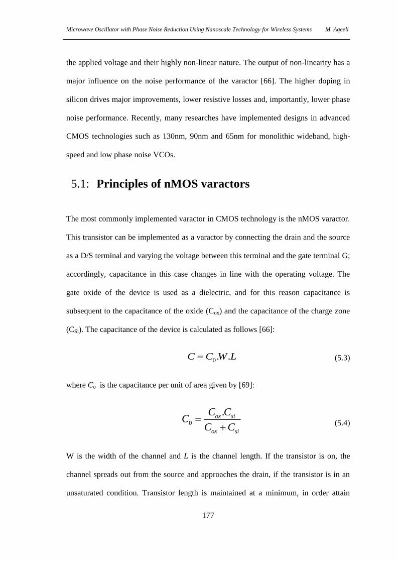
Microwave Oscillator with Phase Noise Reduction Using Nanoscale Technology for Wireless Systems M. Aqeeli
177
the applied voltage and their highly non-linear nature. The output of non-linearity has a
major influence on the noise performance of the varactor [66]. The higher doping in
silicon drives major improvements, lower resistive losses and, importantly, lower phase
noise performance. Recently, many researches have implemented designs in advanced
CMOS technologies such as 130nm, 90nm and 65nm for monolithic wideband, high-
speed and low phase noise VCOs.
5.1: Principles of nMOS varactors
The most commonly implemented varactor in CMOS technology is the nMOS varactor.
This transistor can be implemented as a varactor by connecting the drain and the source
as a D/S terminal and varying the voltage between this terminal and the gate terminal G;
accordingly, capacitance in this case changes in line with the operating voltage. The
gate oxide of the device is used as a dielectric, and for this reason capacitance is
subsequent to the capacitance of the oxide (Cox) and the capacitance of the charge zone
(CSi). The capacitance of the device is calculated as follows [66]:
0. .C C W L (5.3)
where Co is the capacitance per unit of area given by [69]:
0
.ox si
ox si
C CC
C C
(5.4)
W is the width of the channel and L is the channel length. If the transistor is on, the
channel spreads out from the source and approaches the drain, if the transistor is in an
unsaturated condition. Transistor length is maintained at a minimum, in order attain

Microwave Oscillator with Phase Noise Reduction Using Nanoscale Technology for Wireless Systems M. Aqeeli
178
minimum power consumption and high-speed performance. The nMOS varactor stands
out particularly, due to its asymmetric nature, in that the values of its parameter tuning
range and capacitance vary if they are examined from the diffusion terminals or from
the gate. Furthermore, from the area point of view, nMOS varactors are very effective.
The maximum capacitance per unit of area is approximately 300% higher than that of a
PN-junction varactor with obtained the quality factor almost very close to the PN-
junction and will be improved with the technology progression. In addition, the
Cmax/Cmin ratio becomes better in comparison with PN-junction varactors. The
performance of an nMOS varactor should be a compromise between the capacitance
value and the Q factor. Capacitance is at its maximum level when Q reaches its
minimum point [57]. Two operational modes are synonymous with nMOS varactors:
the inversion mode and the accumulation mode.
The accumulation mode is the most commonly used in nMOS varactors; however, an
accumulation-mode MOS varactor is usually a special structure, with its source and
drain doped in the same polarity of the well. As a result, in this research, an nMOS
varactor in inversion mode will be implemented in the proposed LC-VCO. It is
necessary to mention that the nMOS varactor structure in the accumulation mode is
virtually identical to that of an n-channel MOSFET transistor. The only difference is
that it is made in an n well rather than placed directly on the P substrate, as shown in
Figure 5.1. This method removes the parasitic capacitances of the PN-junction that exist
between the P substrate and the source and the drain, which would otherwise restrict the
tuning range. The drain/source is shorted together, and the bulk of the nMOS transistor
is connected to the ground. The operating mode of the transistor is controlled by the VGS
voltage [70].
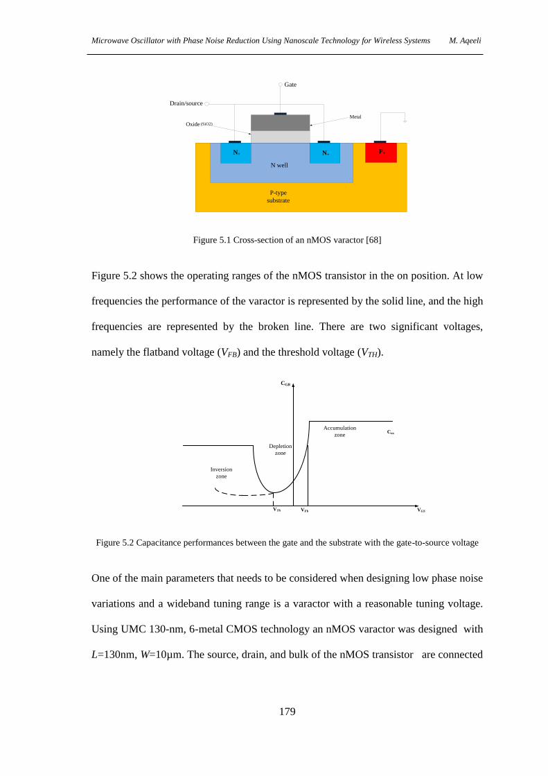
Microwave Oscillator with Phase Noise Reduction Using Nanoscale Technology for Wireless Systems M. Aqeeli
179
N+P+N+
Metal
Drain/source
Gate
P-type
substrate
N well
Oxide (SiO2)
Figure 5.1 Cross-section of an nMOS varactor [68]
Figure 5.2 shows the operating ranges of the nMOS transistor in the on position. At low
frequencies the performance of the varactor is represented by the solid line, and the high
frequencies are represented by the broken line. There are two significant voltages,
namely the flatband voltage (VFB) and the threshold voltage (VTH).
Accumulation
zone
Depletion
zone
Inversion
zone
VFbVTh VGS
Cox
CGB
Figure 5.2 Capacitance performances between the gate and the substrate with the gate-to-source voltage
One of the main parameters that needs to be considered when designing low phase noise
variations and a wideband tuning range is a varactor with a reasonable tuning voltage.
Using UMC 130-nm, 6-metal CMOS technology an nMOS varactor was designed with
L=130nm, W=10µm. The source, drain, and bulk of the nMOS transistor are connected

Microwave Oscillator with Phase Noise Reduction Using Nanoscale Technology for Wireless Systems M. Aqeeli
180
to the tuning voltage as shown in Figure 5.3. The simulation results provide both an
inversion and an accumulation mode curve, as shown in Figure 5.4.
Figure 5.3 Simulated nMOS varactors with source, drain and bulk connected to the tuning voltage
-3 -2 -1 0 1 2 3
45.0f
50.0f
55.0f
60.0f
65.0f
70.0f
75.0f
Ca
pacita
ncw
e (
F)
Tuning voltage (V)
nMOS varactor
Figure 5.4 Typical capacitance curve of an nMOS varactor with source, drain and bulk connected to the
tuning voltage

Microwave Oscillator with Phase Noise Reduction Using Nanoscale Technology for Wireless Systems M. Aqeeli
181
A varactor bank contains four nMOS transistors which are designed and connected in
parallel with L=130nm, W=10µm using UMC 130-nm, 6-metal CMOS technology.
This takes advantage of the ability of the tuning curve of the varactor bank to be shifted
using different bias-voltages. The different selected biasing voltages are selected to be:
0.4, 0.8, 1.6 and 3.2 V, to basically shifted curves, as depicted in Figure 5.5. The overall
tuning characteristic of the varactor bank will be implemented in this study to extend
the tuning range due to overlapping between linear tuning ranges among the varactor
bank.
-3 -2 -1 0 1 2 3
45.0f
50.0f
55.0f
60.0f
65.0f
70.0f
75.0f
Ca
pa
cita
ncw
e (
F)
Tuning voltage (V)
nMOS varactor
0.4 V
0.8 V
1.6 V
3.2 V
Figure 5.5 Typical capacitance curves of an nMOS varactor with its source, drain and bulk connected to
the tuning voltage at different biasing gate voltages
5.1.1: Accumulation mode varactors
An nMOS varactor works in accumulation mode when the gate-source DC voltage is
greater than the flat-band DC voltage VGS > VFB. Electrons accumulate on the silicon

Microwave Oscillator with Phase Noise Reduction Using Nanoscale Technology for Wireless Systems M. Aqeeli
182
surface below the oxide from the zones N+, as shown in Figure 5.6, while the holes are
expelled. Therefore, total capacitance, Ctotal, is the outcome of the two capacitance
series Cox and CSi. An AMOS varactor is not readily available in any design kit. This is
especially true for the UMC-130nm [12].
N+P+N+
Metal
Drain/source
Gate
P-type
substrate
Oxide (SiO2)
-------
+++++++
Free holes
Free electrons
Figure 5.6 nMOS varactor working in accumulation mode [11]
5.1.2: Depletion mode varactors
An nMOS varactor operates in depletion mode when VTH < VGS < VFB. Holes are
attracted from the substrate, and as consequence depletion zones are produced around
the N+ diffusions (Cd), as shown in Figure 5.7, just underneath the gate oxide CSi. The
total capacitance of the varactor will be the combination of CSi, Cox and Cd. The size of
the depletion zone will depend on the applied DC voltage, increasing or reducing CSi
and Cd. Consequently, the minimum value of total capacitance is achieved when
VGS = VTH. Observing this point for varactor design, the advantage of the depletion
operating mode in comparison with the accumulation mode is that it is likely to control
the capacitance value through the voltage between its terminals [12].

Microwave Oscillator with Phase Noise Reduction Using Nanoscale Technology for Wireless Systems M. Aqeeli
183
N+P+N+
Metal
Drain/source
Gate
P-type
substrate
--------------
+ +
Oxide (SiO2)
+
Fixed donator ions
Fixed acceptor ions
Figure 5.7 An nMOS varactor working in depletion mode [12]
5.1.3: Inversion mode varactors
An inversion zone is formed under the gate when the gate-source voltage continues to
decrease, i.e. VGS < VTH, as shown in Figure 5.8. Operating in the inversion zone at low
frequencies demonstrates an increase in the device capacitance almost at the maximum
value (Cox,max). The maximum capacitance value per unit of area, C0,max, is equal to ε/tox,
which is very similar to the high accumulation value directly below the gate oxide. The
minimum capacitance value per unit of area, C0,min, is achieved when the difference
between the voltages of electrodes in the device is equal to the VTH magnitude. The
tuning range can be defined by the ratio between Cox and C0,min. The nMOS varactor
behaves differently when the DC voltage applied between its terminals is not the exact
value [12].

Microwave Oscillator with Phase Noise Reduction Using Nanoscale Technology for Wireless Systems M. Aqeeli
184
N+P+N+
Metal
Drain/source
Gate
P-type
substrate
---------------------
+
Oxide (SiO2)
++++++
Fixed donator ions
Free electrons
Fixed acceptor ions
Figure 5.8 nMOS varactor working in inversion mode [12]
In order to determine the capacitance value of an nMOS varactor in inversion mode, the
circuit shown in Figure 5.9 was designed, containing two nMOS transistors with both
bulks connected to 0V or the ground. If biasing throughout the resistor is ignored for a
while, and consider the following situation: bulk is connected to 0V, the gate is
connected to 0V and Source/ drain are connected to -1 V, this will lead to the situation
on the left side of the plots shown in Figure 5.10. It might not be easy to visualise, but
the MOSFET is in inversion. As the tuning voltage increases, Vtune to 0 V, the inversion
layer disappears, but further increases Vtune to 1.0 V and above, though this does not
result in accumulation. If the bias voltage is set to positive values throughout the
resistor, then the result are basically shifted curves [12].

Microwave Oscillator with Phase Noise Reduction Using Nanoscale Technology for Wireless Systems M. Aqeeli
185
Figure 5.9 Simulated nMOS varactors with source and drain connected to
the tuning voltage and bulk connected to the ground
-3 -2 -1 0 1 2 3
3.5x10⁻¹⁴
4.0x10⁻¹⁴
4.5x10⁻¹⁴
5.0x10⁻¹⁴
5.5x10⁻¹⁴
6.0x10⁻¹⁴
6.5x10⁻¹⁴
7.0x10⁻¹⁴
7.5x10⁻¹⁴
Ca
pacita
nce
(F)
Tuning voltage(V)
nMOS varactor in inversion mode
Figure 5.10 Capacitance of the nMOS varactor in inversion mode

Microwave Oscillator with Phase Noise Reduction Using Nanoscale Technology for Wireless Systems M. Aqeeli
186
A varactor bank contains five nMOS varactors in inversion mode which are designed
and connected in parallel with L=130nm, W=10µm using UMC 130-nm, 6-metal CMOS
technology. Taking advantage of the ability of the tuning curve of the varactor bank to
be shifted using different bias-voltages, the different selected biasing voltages to
positive values through the resistor are: 0.2 0.4, 0.8, 1.6 and 3.2 V. In this case, a
basically shifted curves is achieved, as depicted in Figure 5.11. The overall tuning
characteristic of the varactor bank will be employed in this study to extend the tuning
range due to overlapping between the tuning ranges in the varactor bank. As a result, the
gain of the proposed LC-VCO will decrease compared to conventional designs.
Importantly, phase noise variations will decrease, as will be shown in Chapter 7.
-3 -2 -1 0 1 2 3
3.5x10⁻¹⁴
4.0x10⁻¹⁴
4.5x10⁻¹⁴
5.0x10⁻¹⁴
5.5x10⁻¹⁴
6.0x10⁻¹⁴
6.5x10⁻¹⁴
7.0x10⁻¹⁴
7.5x10⁻¹⁴
Ca
pa
cita
nce
(F
)
Tuning voltage (V)
nMOS varactor in inversion mode
BV=0.2V
BV=0.4V
BV=3.2V
BV=1.6V
BV=0.8V
Figure 5.11 Simulated capacitance of the five nMOS varactor banks in inversion mode
different gate-basing voltages

Microwave Oscillator with Phase Noise Reduction Using Nanoscale Technology for Wireless Systems M. Aqeeli
187
5.2: Operating mode influence on an nMOS varactor
It was mentioned above that nMOS varactors have an accumulation mode and an
inversion operating mode. It is necessary to mention here that the only difference
between the two configurations is that in accumulation varactors an N well is present in
the channel between the drain and the source, as shown in Figure 5.12 (a), which
depicts a cross-section in comparison with nMOS varactors working in the inversion
mode shown in Figure 5.12 (b). This divergence makes the voltage behave differently in
both configurations. The variation of the capacitance with the bias voltage of the
varactors working in the accumulation and the inversion operating modes is shown in
Figure 5.13. When a positive DC voltage is applied to the gate of an nMOS varactor in
accumulation mode, total capacitance is fundamentally specified by Cox [71].
N+ N+
Drain/source
Gate
P-type
substrate
N well
N+ N+
Drain/source
Gate
P-type
substrate
(a) Accumulation mode (b) Inversion mode
Figure 5.12 Two operating modes of an nMOS varactor

Microwave Oscillator with Phase Noise Reduction Using Nanoscale Technology for Wireless Systems M. Aqeeli
188
-3.5 -1.5-2.5 -0.5 +0.5 +1.5 +2.5 +3.51.0
1.5
2.0
2.5
3.5
3.0
4.0
Bias voltage (V)
Cap
acit
ance
(pF
)
nMOS Varactor in accumulation mode
nMOS Varactor in inversion mode
Figure 5.13 Influence of the operating mode
5.2.1: Influence of the geometrical parameters on an nMOS
varactor
This section presents the influence of geometrical parameters on the operation of an
nMOS varactor working in the inversion mode. These parameters explore varactor size,
gate length and gate width.
Influence of gate length variations 5.2.1.1:
A very important parameter in any CMOS varactor is length. The influence of the gate
length is analysed through three nMOS varactors in the inversion mode with three gate
lengths: 130nm, 250nm and 340nm, are chosen, the variation of the capacitance with
the tuning voltage of the three varactors are simulated as shown in Figure 5.14. It is

Microwave Oscillator with Phase Noise Reduction Using Nanoscale Technology for Wireless Systems M. Aqeeli
189
clearly evident that increments in capacitance value are not equal around the zero
voltage.
-3 -2 -1 0 1 2 3
30.0f
40.0f
50.0f
60.0f
70.0f
80.0f
90.0f
100.0f
110.0f
Cap
acitan
ce (
F)
Tuning voltage (V)
10
130
W m
L nm
10
250
W m
L nm
10
360
W m
L nm
Figure 5.14 Impact of gate length of an nMOS varactor with tuning voltage
Impact of variations in varactor size 5.2.1.2:
An nMOS varactor was designed using nMOS transistors in the inversion mode,
connected in parallel with the same width and a different number of devices.
Figure 5.15 depicts variations in capacitance with the tuning voltage for four different
varactors constructed with one transistor, four transistors, six transistors and 12
transistors.
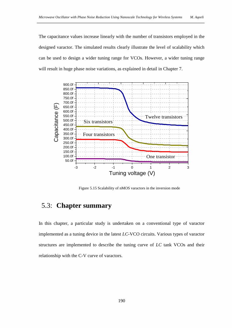
Microwave Oscillator with Phase Noise Reduction Using Nanoscale Technology for Wireless Systems M. Aqeeli
190
The capacitance values increase linearly with the number of transistors employed in the
designed varactor. The simulated results clearly illustrate the level of scalability which
can be used to design a wider tuning range for VCOs. However, a wider tuning range
will result in huge phase noise variations, as explained in detail in Chapter 7.
-3 -2 -1 0 1 2 3
50.0f
100.0f
150.0f
200.0f
250.0f
300.0f
350.0f
400.0f
450.0f
500.0f
550.0f
600.0f
650.0f
700.0f
750.0f
800.0f
850.0f
900.0f
Ca
pa
cita
nce
(F
)
Tuning voltage (V)
Four transistors
One transistor
Six transistorsTwelve transistors
Figure 5.15 Scalability of nMOS varactors in the inversion mode
5.3: Chapter summary
In this chapter, a particular study is undertaken on a conventional type of varactor
implemented as a tuning device in the latest LC-VCO circuits. Various types of varactor
structures are implemented to describe the tuning curve of LC tank VCOs and their
relationship with the C-V curve of varactors.

Microwave Oscillator with Phase Noise Reduction Using Nanoscale Technology for Wireless Systems M. Aqeeli
191
Digitally Controlled Chapter 6:
Microwave VCO with a
Wide Tuning Range and
Low Phase Noise Variation
6.1: Introduction
The design of VCOs is challenging, due to the limited characteristics of available
varactors. High Q factor varactors regularly have narrower tuning ranges, and as a
result, the reduction of phase noise at a certain frequency as well as phase noise
variations commonly reveal the undesirable presence of manufacturing errors. Standard
CMOS technology offers diodes and MOS capacitors as varactors. nMOS in
accumulation mode and pMOS in inversion mode varactors [51, 72-74] can provide a
significant VCO tuning range, while Q factor variations close to the VTH cause phase
noise in the LC-VCO to fluctuate dramatically in line with the control voltage, as

Microwave Oscillator with Phase Noise Reduction Using Nanoscale Technology for Wireless Systems M. Aqeeli
192
mentioned in Chapter one. Phase noise variations vary dramatically over the wide
tuning range of VCOs.
For low phase noise, it is necessary to have as little gain as possible. However, this
small KVCO means a narrow frequency locking range [75]. Standard CMOS technology
offers diodes and MOS capacitors as varactors. In some designs, phase noise variations
exceed 25dB [44]. In a wide tuning range, variations between the minimum and the
maximum values of the frequencies (fmax-fmin) can be large, meaning large variations in
KVCO. As proof of this theory, and to compare between the studies presented in this
thesis and published work, the pMOS-only VCO design with body-bias varactors
presented in [76] was constructed using the same parameters mentioned in the published
work.
The simulation results show clearly that the achieved tuning ranges from
4.40 to 5.43 GHz with phase noise variation of more than 16 dBc/Hz at 1 MHz offset,
as shown in Figure 6.1, although the claimed measured phase noise was -138.4 dBc/Hz
at a 1 MHz offset. Therefore, there must be a solution to this conflict and a trade-off
between the frequency tuning range and KVCO variations. As phase noise performance is
directly proportional to gain, KVCO, a large KVCO will amplify noise coupling to the
control node, and as a consequence it will degrade phase noise performance. According
to information available to the authors, it seems that this problem is not as widely
acknowledged in the literature as perhaps it should be.

Microwave Oscillator with Phase Noise Reduction Using Nanoscale Technology for Wireless Systems M. Aqeeli
193
PN=-116.8dBc/Hz @ 5GHz
PN=-133dBc/Hz @ 4.4GHz
4.4 4.6 4.8 5.0 5.2 5.4
-135
-130
-125
-120
-115
-110
Ph
ase
no
ise
at
1M
Hz o
ffse
t (d
Bc/H
z)
Frequency of operation (GHz)
Body- biased pMOS varactor
Figure 6.1 Phase noise of VCOs with a body-biased pMOS varactor
KVCO variation issues must be considered carefully when the tuning range of a VCO
becomes very wide. KVCO variations increase in line with the frequency tuning range of
the VCO, which in turn creates an obstruction to optimising the performance of the
PLL. In addition, using an MOS transistor as a varactor will increase the probability of
converting AM noise to FM noise [77]. Therefore, switching capacitors are mandatory
for maintaining minimum phase noise, tuning linearity and achieving low VCO
sensitivity when the tuning range is more than 30% [14].
Studies using switching capacitors inside the LC tank have been conducted, in order to
extend the tuning range and improve VCO phase noise [52, 72, 78, 79]
. These
techniques are effective in widening frequency tuning, improving phase noise
performance and lowering KVCO. However, the measured phase noise has been relatively
Microwave Oscillator with Phase Noise Reduction Using Nanoscale Technology for Wireless Systems M. Aqeeli
194
high, varying from -90.2 dBc/Hz to -122 dBc/Hz. The resistors in all the presented
works used switches that were implemented from stacked devices and large resistors for
DC biasing of the S/D terminals of the MOS switch [80]. These large resistors tend to
be implemented to gain high impedance for RF signals, resulting in occupying a larger
die area as well as exhibiting higher power dissipation and phase noise. Mostly
important a higher parasitic capacitances are added to critical RF nodes which will
cause a degradation of phase noise. In addition, it is proven that specific CMOS
resistances range from a few tens of Ω/ to only a few kΩ/ Therefore, it can be
beneficial to have resistors up to a few hundred ohm [1], while on the other hand it
becomes a serious obstacle when reaching a thousands of kilo-ohms, which are the
required values for DC biasing resistors.
6.2: Circuit design and implementation
The VCO core is based on a standard LC-tuned complementary cross-coupled
topology as shown in Figure 6.2 . It is composed by two blocks of cross-coupled pair
transistors –pMOS (W/L=50µm/130nm), nMOS (W/L=50µm/130nm), LC tank and a
current source. This configuration was chosen for this work because the structure
offers higher transconductance, better rise- and fall-time symmetry and the active
devices serve as a negative resistor to compensate for energy loss from the tank due to
the tank’s effective resistor. Another advantage of this topology is its ability to achieve
low phase noise compared to other configurations. The LC-tank of the proposed VCO
is mainly composed of a single integrated differential spiral inductor, a varactor bank
(inversion-mode MOS varactors) and a high-quality digital switching array providing
coarse tuning steps, to obtain linear tuning curves, minimum KVCO and minor phase

Microwave Oscillator with Phase Noise Reduction Using Nanoscale Technology for Wireless Systems M. Aqeeli
195
noise variations. To sustain oscillations, VCO must satisfy the Barkhausen criteria.
The oscillation will occur when the loop gain has a zero phase shift with a magnitude
of one at the oscillation frequency. Practically, the oscillator the start-up loop-gain
magnitude should be greater than one in order for oscillations to build up to the
steady-state amplitude that is limited by other nonlinear effects. The oscillation
frequency is also affected by the bias current. The proposed design utilizes a direct
bias current source rather than the conventional mirrored bias current. The bias current
of the VCO, which is an important parameter for phase noise optimization, is designed
to handle the maximum current allowed by the specifications. Therefore, a biasing
current source is designed with a capacitor Cx is inserted in parallel with the transistor
M1 to filter the tail transistor noise. Cp is the source node capacitance which causes
the oscillation frequency to increase. To solve the loading problem, an inductor with a
value of Lx is inserted between the drain of the tail transistor M1 and the source node
of the cross-coupled transistors. Due to the fact that poor output isolation can produce
various mechanisms which cause disturbance to the VCO performance, therefore, a
buffer stage is necessary to be included at oscillator outputs. Isolation between two
circuit stages is often achieved by introducing a buffer amplifier between them. This
isolation minimizes adverse effects in a wide range of applications. The LC-tank
output buffer was designed to facilitate the simulations and the future measurements.
Its main function is to deliver sufficient power to drive the 50Ω spectrum analyzer.
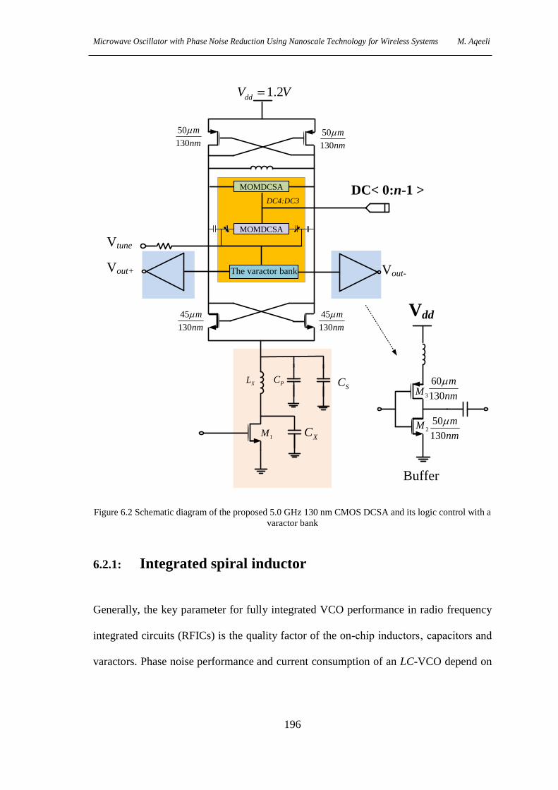
Microwave Oscillator with Phase Noise Reduction Using Nanoscale Technology for Wireless Systems M. Aqeeli
196
DC< 0:n-1 >
Vout-Vout+
Vtune
DC4:DC3
MOMDCSA
MOMDCSA
The varactor bank
50
130
m
nm
50
130
m
nm
45
130
m
nm
45
130
m
nm
XL
XC
PCSC
1M
Vdd
60
130
m
nm
50
130
m
nm
2M
3M
1.2ddV V
Buffer
Figure 6.2 Schematic diagram of the proposed 5.0 GHz 130 nm CMOS DCSA and its logic control with a
varactor bank
6.2.1: Integrated spiral inductor
Generally, the key parameter for fully integrated VCO performance in radio frequency
integrated circuits (RFICs) is the quality factor of the on-chip inductors‚ capacitors and
varactors. Phase noise performance and current consumption of an LC-VCO depend on

Microwave Oscillator with Phase Noise Reduction Using Nanoscale Technology for Wireless Systems M. Aqeeli
197
the quality factor of the LC tank circuit: the higher the Q factor of the tank, the lower
phase noise [81].
The loaded Q factor of the resonator tank is primarily determined by the Q factor of on-
chip inductors and varactors. The major drawback of on-chip inductors is their low
Q factor and large die area. An approach has therefore been implemented and tested in
this work to reduce losses, reduce current consumption, enhance the differential Q
factor and save the silicon area for on-chip inductors in CMOS technology. This
involves reducing metal sheet resistance by using thicker metallisation and lower
resistivity metals [44].
The Q factor of a differential inductor is the same as that of a single-ended inductor at
low frequencies. However, the self-resonance point of a differential transmission line is
at the half-wavelength frequency, whereas a shorted inductor self-resonates
fundamentally at the quarter-wavelength frequency. This means that a differential
inductor self-resonates at an approximately two times higher frequency than a single-
ended inductor. Therefore, the Q factor difference between the two inductors increases
as the operating frequency rises. In addition, another advantage is a reduction of chip
area because of mutual magnetic coupling, which results in less substrate loss at high
frequencies. Required information about the electrical model is supplied through the
Component Description Format (CDF) form in Cadence software [44]. The first field of
this form, “Simulation Information,” handles necessary inputs concerning the
simulation, while the second one, known as “Component Parameters,” is employed to
enter the parameters which describe the model. The layout and its equivalent model of
octagonal differential inductor are shown in Figure 6.3 and Figure 6.4, respectively.
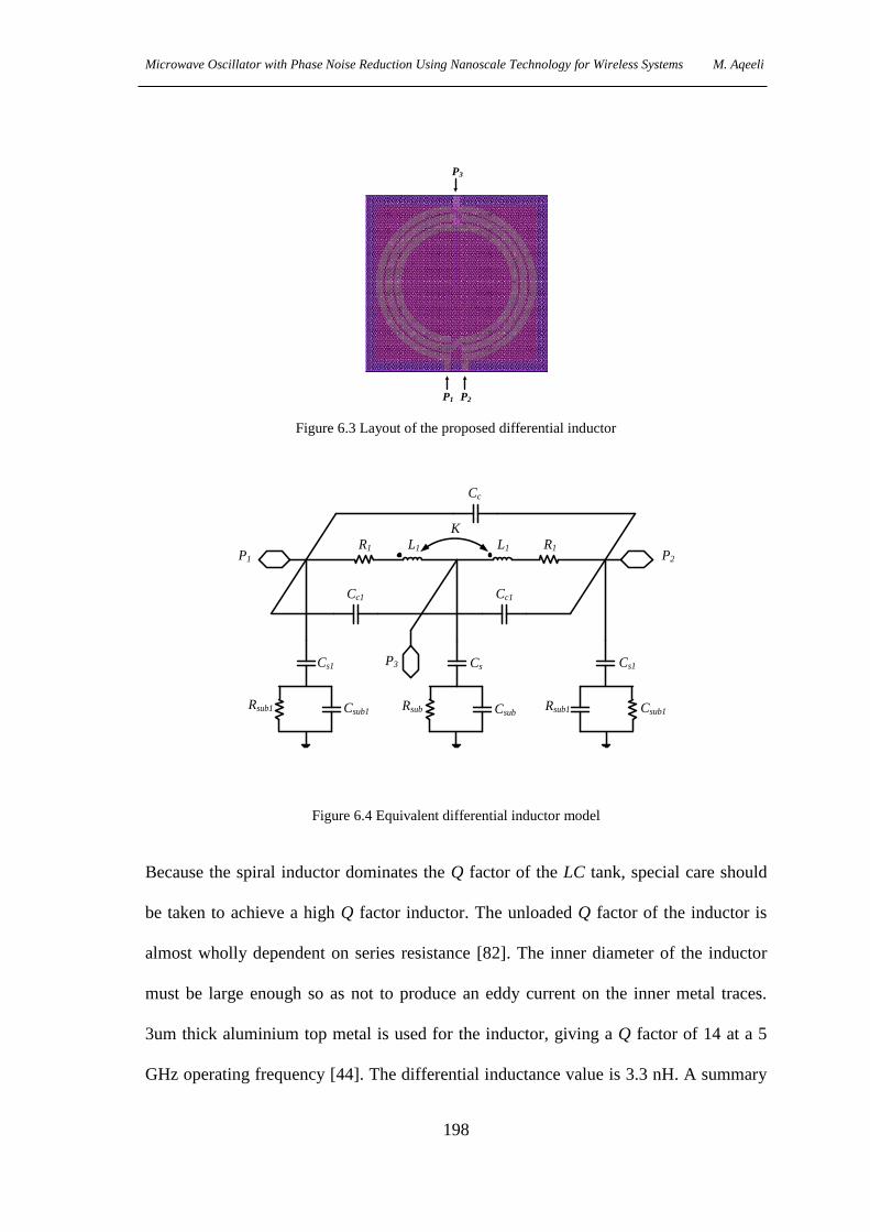
Microwave Oscillator with Phase Noise Reduction Using Nanoscale Technology for Wireless Systems M. Aqeeli
198
P1 P2
P3
Figure 6.3 Layout of the proposed differential inductor
Cc1
Rsub Csub
Cs
Csub1
Cs1
Csub1
Cs1
Rsub1 Rsub1
Cc1
Cc
R1 R1L1L1P2P1
P3
K
Figure 6.4 Equivalent differential inductor model
Because the spiral inductor dominates the Q factor of the LC tank, special care should
be taken to achieve a high Q factor inductor. The unloaded Q factor of the inductor is
almost wholly dependent on series resistance [82]. The inner diameter of the inductor
must be large enough so as not to produce an eddy current on the inner metal traces.
3um thick aluminium top metal is used for the inductor, giving a Q factor of 14 at a 5
GHz operating frequency [44]. The differential inductance value is 3.3 nH. A summary
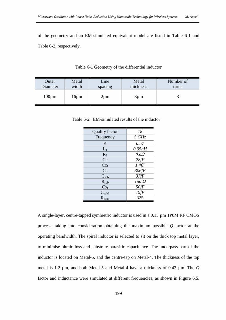
Microwave Oscillator with Phase Noise Reduction Using Nanoscale Technology for Wireless Systems M. Aqeeli
199
of the geometry and an EM-simulated equivalent model are listed in Table 6-1 and
Table 6-2, respectively.
Table 6-1 Geometry of the differential inductor
Outer
Diameter
Metal
width
Line
spacing
Metal
thickness
Number of
turns
100µm 16µm 2µm 3µm 3
Table 6-2 EM-simulated results of the inductor
Quality factor 18
Frequency 5 GHz
K 0.57
L1 0.95nH
R1 0.6Ω
Cc 28fF
Cc1 1.4fF
Cs 306fF
Csub 37fF
Rsub 160 Ω
Cs1 50fF
Csub1 19fF
Rsub1 325
A single-layer, centre-tapped symmetric inductor is used in a 0.13 µm 1P8M RF CMOS
process, taking into consideration obtaining the maximum possible Q factor at the
operating bandwidth. The spiral inductor is selected to sit on the thick top metal layer,
to minimise ohmic loss and substrate parasitic capacitance. The underpass part of the
inductor is located on Metal-5, and the centre-tap on Metal-4. The thickness of the top
metal is 1.2 µm, and both Metal-5 and Metal-4 have a thickness of 0.43 µm. The Q
factor and inductance were simulated at different frequencies, as shown in Figure 6.5.
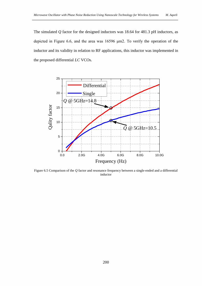
Microwave Oscillator with Phase Noise Reduction Using Nanoscale Technology for Wireless Systems M. Aqeeli
200
The simulated Q factor for the designed inductors was 18.64 for 481.3 pH inductors, as
depicted in Figure 6.6, and the area was 16596 μm2. To verify the operation of the
inductor and its validity in relation to RF applications, this inductor was implemented in
the proposed differential LC VCOs.
Q @ 5GHz=14.8
Q @ 5GHz=10.5
0.0 2.0G 4.0G 6.0G 8.0G 10.0G
0
5
10
15
20
25
Qal
ity
fac
tor
Frequency (Hz)
Differential
Single
Figure 6.5 Comparison of the Q factor and resonance frequency between a single-ended and a differential
inductor

Microwave Oscillator with Phase Noise Reduction Using Nanoscale Technology for Wireless Systems M. Aqeeli
201
0.00 2.50G 5.00G 7.50G 10.00G
480.0p
482.0p
484.0p
486.0p
488.0p
490.0p
492.0p
494.0p
496.0p
498.0p
500.0p Quality factor
Inductance
Frequency (Hz)
Ind
ucta
nce (
H)
0
6
12
18
24
30
Quali
ty f
acto
r (Q
)
Figure 6.6 Inductor values and quality factor of the centre-tapped differential inductor versus frequency
6.2.2: Varactor for low phase noise variation
Phase noise can be analysed using Lee and Hajimiri’s
model [21]. LC tank VCOs can
be viewed as a parallel combination of a lossy LC tank with a negative resistance, as
shown in Figure 6.7.
Vout-
Z(o+∆)
LPCPRP-RP in
Figure 6.7 Small signal equivalent circuit of the VCO [21]

Microwave Oscillator with Phase Noise Reduction Using Nanoscale Technology for Wireless Systems M. Aqeeli
202
Negative resistance must compensate for the loss of the LC tank’s parallel resistance,
RP. At resonance the impedance of an LC-VCO tank may be approximated as:
0
0 0[ ( )]2
pRZ jZ j
Q
(6.1)
where Q is the quality factor of the LC tank. The relationship between phase noise and
gain KVCO at the output of the VCO can be shown as [72]
22 2_
0 0 2
0
1( ) . .
2
VCO VCOn n
K KS Z
S Qi
(6.2)
where KVCO is the gain of the VCO, 0 is the carrier frequency, ∆ 0 is the offset
frequency,
2_
ni is the mean square noise current spectral density and Q is the quality
factor of the LC tank. Equation (6.2) shows clearly that the phase noise of the VCO is
proportional to the square of the VCO gain. As discussed above, in order to obtain
better phase noise with minimal variations, both VCO tuning gain and an extended
linear tuning range are necessary. A wide tuning range is achieved by switching
capacitors in popular wideband VCOs, in which the switched capacitors can be fixed
capacitors or varactors. However, this leads to KVCO and phase noise varying greatly
over different sub-bands.

Microwave Oscillator with Phase Noise Reduction Using Nanoscale Technology for Wireless Systems M. Aqeeli
203
MOMDCSA in parallel with a gain-linearised varactor 6.2.2.1:
Switched capacitors have worse phase noise due to their lower quality factor than fixed
capacitors, as well as noise from large resistors used for DC biasing of the S/D terminals
in MOS switch devices being modulated directly to phase noise. To achieve a wide
tuning range for lower phase noise and minimal variations, a set metal-oxide-metal
(MOM) digital switching capacitors array (DSCA) is added in parallel to nMOS
varactors, to divide the tuning range into multiple bands. Importantly, previous employed
resistors [52, 72, 83] have been replaced with much smaller nMOS transistors [84, 85]
which perform as resistors. These in turn occupy a much smaller area, resulting in less
parasitic capacitance affecting the RF nodes of the VCO. For further gain, linearise and
minor phase noise variations, each pair of nMOSvaractors is biased at different voltages,
namely 0.8, 1.6 and 3.2V, to shift the tuning curves of varactors. The control signal for
each group in the varactor bank is correlated with the control signal for the binary
weighted switched-capacitor bank. Such an approach enables the VCO to have an
extended tuning bandwidth and minimises phase noise variations throughout the entire
tuning range while maintaining minimum die size. nMOS transistors are employed as
varactors instead of pMOS transistors, because they occupy a smaller die area compared
to pMOS transistors‚ and thus fewer parasitic capacitances are added to the VCO core.
Such an arrangement will extend the linear tuning range of the varactors and,
importantly, reduce the KVCO, phase noise and phase noise variations. In order to reduce
phase noise variations it is necessary to find the VCO design parameters which will
compensate for the KVCO disparities. To understand the effect of the proposed varactor,
one has to derive the expression for the gain and the varactor. The MOMDCSA varactor
consists of MOMDCSA is connected in parallel with the nMOS varactor pair and the
Microwave Oscillator with Phase Noise Reduction Using Nanoscale Technology for Wireless Systems M. Aqeeli
204
DSVB is implemented, to divide the tuning range into multiple frequency bands. Equal
step sizes for the MOM capacitor values (CMOM, 2CMOM, 4CMOM…2N-1
CMOM ) and nMOS
device switch widths (WN, 2WN, 4WN... 2N-1
WN) are used to provide binary-weighted
switching steps. The DCSA capacitance value can be calculated as [1]:
1
1 1(2 1)N
MOM DF
CC C
(6.3)
where CMOM is the capacitance of the DCSA, and CDF is the drain fringe capacitance of
the switch devices. Total capacitance C of the series MOMDCSA, including fixed
parasitic capacitance of the active devices. Total capacitance SC of the MOMDCSA
array is equal to:
1
1 1(2 1)N
S PAR
MOM DF
C CC C
(6.4)
where DFC is the drain fringe capacitance of the parallel MOMDCSA. Total capacitance
Cγ of the nMOS varactor and the series MOMDCSA can be calculated as:
S VarC C C (6.5)
where CVar is the total capacitance of the nMOS varactor. The oscillation frequency (fosc)
of the VCO can be written as follows:
1
2Osc
S Var
fL C C
(6.6)
KVCO can be derived as follows:

Microwave Oscillator with Phase Noise Reduction Using Nanoscale Technology for Wireless Systems M. Aqeeli
205
3/ 2
1 1. .( )4
Osc VarVCO
Cont S Var Cont
f CK
V C C VL
(6.7)
where Vcont is the controlled voltage. Equation (6.7) demonstrates that the gain of the
proposed VCO is a function of the LC tank. Consequently, the gain KVCO is gradient of
the frequency-voltage relationship. The proposed VCO has many advantages, such as
providing an accepted solution to the problem of high phase noise variations associated
with wideband tuning, and minimising the sensitivity of the VCO by optimising gain.
Finally, it has an output frequency which varies linearly with the control voltage. The
LC-VCO has been designed and simulated using a UMC-130 nm mixed-mode CMOS.
The VCO has a tuning range from 4.45 GHz to 5.78 GHz, which varies linearly with the
control voltage. Clearly, the proposed MOMDCSA topology with the gain linearised
nMOS varactor bank has better characterisations than the work presented in [76],
which employed a pMOS varactor with a more significant effect on phase noise
reduction variations. The high-performance VCO specifications include phase noise
measured at -132.5 dBc/Hz at an offset frequency of 1 MHz away from the 5.0 GHz,
phase noise variations of less than 12.7 dBc/Hz and KVCO variations equal to
23.5MHz/V, as shown in Figure 6.8.
Microwave Oscillator with Phase Noise Reduction Using Nanoscale Technology for Wireless Systems M. Aqeeli
206
30
35
40
45
50
55
60
Kvco (MHz/V)
Phase noise(dBc/Hz)
Coarse control code
Kvco @
1.0
V(M
Hz/V
)
-138
-136
-134
-132
-130
-128
-126
-124
-122
Pha
se
no
ise (
dB
c/H
z)
23
.5 M
Hz/
V
12.7
dB
c/H
z
0000 0001 0010 0011 0100 0101 0110 0111 1000 1001 1010 1011 1100 1101 1110 1111
Figure 6.8 KVCO and phase noise of the proposed VCO with DCSA connected in parallel to the varactor
bank
The derived FoM is -202.8 dBc/Hz, while the VCO core’s total power consumption is
2.9 mW away from a 3.2V supply voltage. The output peak-to-peak voltage of the VCO
is 2.8 V, with spurious harmonics at < 32 dBm. As proof of the concept, the
performance of the novel VCO in this study is compared to a previously designed VCO
with a body biased pMOS varactor bank implemented, using the same technology. The
results show clearly in Table 6-3 that the novel VCO is the best in terms of phase noise,
power dissipation, ultra-bandwidth and a better FoM.

Microwave Oscillator with Phase Noise Reduction Using Nanoscale Technology for Wireless Systems M. Aqeeli
207
Table 6-3A comparison of the two VCOs, one with MOMDCSA in parallel to a pMOS
varactor bank and the second with MOMDCSA in parallel to a gain-linearised nMOS
varactor bank
Parameter
A
B
Phase Noise Variances (dBc/Hz) 16.3 ∼12.7
Phase Noise at Centre Frequency (dBc/Hz) -132.20 -132.50
FoM@1MHz Offset(dBc/Hz) -195.6 -202.8
Tuning Range (GHz) 4.45 -5.43 4.45-5.78
KVCO Variation (MHz/V) 36.2 23.5
Spurious harmonics (dBm) 25 32
Power Consumption (mW) 13.1 2.9
A: MOMDCSA in parallel to a pMOS varactor bank.
B: MOMDCSA in parallel to a gain-linearised nMOS varactor bank [25] PN: Phase Noise
MOMDCSA in series and parallel to a varactor bank 6.2.2.2:
In this subsection, an extended approach to gain linearisation will be introduced, in
order to provide a significant improvement in VCO phase noise performance. To
achieve a wide tuning range for lower phase noise and minimum variation, two sets of
DCSA are used in the proposed VCO. The first one is in series with the nMOS
varactors, and the second is in parallel with the inductor, to divide the tuning range into
multiple frequency bands. Such an arrangement will extend the linear tuning range of
the varactors and, importantly, reduce the KVCO and phase noise variation [84]. It was
found that this topology provides a relatively constant output swing frequency and
minimal phase noise over the operating frequency range. Consequently, phase noise
variation challenges were optimised. The operation of the DCSA was implemented
using symmetric-type MOM capacitors (capacitor device architecture is illustrated in
Appendix C), because of their large capacitance, low parasitic capacitance, symmetrical
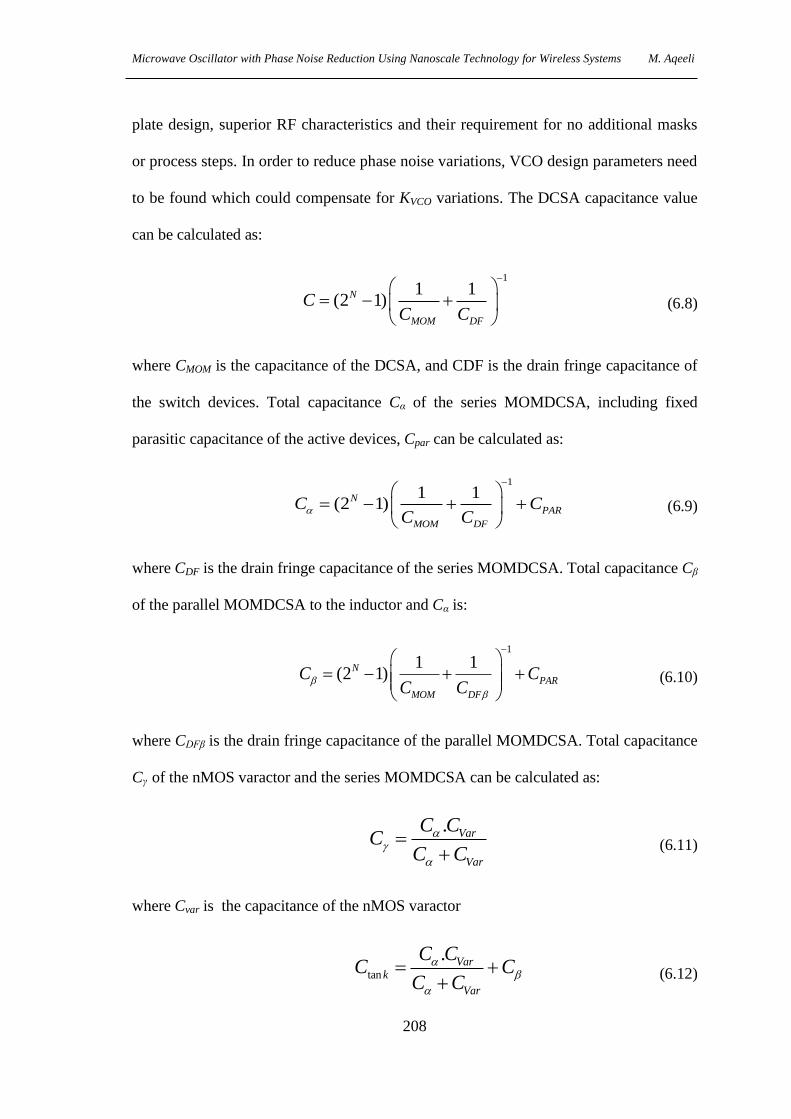
Microwave Oscillator with Phase Noise Reduction Using Nanoscale Technology for Wireless Systems M. Aqeeli
208
plate design, superior RF characteristics and their requirement for no additional masks
or process steps. In order to reduce phase noise variations, VCO design parameters need
to be found which could compensate for KVCO variations. The DCSA capacitance value
can be calculated as:
1
1 1(2 1)N
MOM DF
CC C
(6.8)
where CMOM is the capacitance of the DCSA, and CDF is the drain fringe capacitance of
the switch devices. Total capacitance Cα of the series MOMDCSA, including fixed
parasitic capacitance of the active devices, Cpar can be calculated as:
1
1 1(2 1)N
PAR
MOM DF
C CC C
(6.9)
where CDF is the drain fringe capacitance of the series MOMDCSA. Total capacitance Cβ
of the parallel MOMDCSA to the inductor and Cα is:
1
1 1(2 1)N
PAR
MOM DF
C CC C
(6.10)
where CDFβ is the drain fringe capacitance of the parallel MOMDCSA. Total capacitance
Cγ of the nMOS varactor and the series MOMDCSA can be calculated as:
. Var
Var
C CC
C C
(6.11)
where Cvar is the capacitance of the nMOS varactor
tan
. Vark
Var
C CC C
C C
(6.12)

Microwave Oscillator with Phase Noise Reduction Using Nanoscale Technology for Wireless Systems M. Aqeeli
209
The oscillation frequency (fosc) of the VCO can be written as follows:
1
2 [( . ) ]Osc
Var Var
fL C C C C C
(6.13)
KVCO can be derived as follows:
Assuming:
( ) .Var
Var
C C C C CC
C C
(6.14)
then:
2
23/ 2
1. .( )4 .
Osc VarVCO
Cont Var Cont
f C CK
V C C VL C
(6.15)
where Vcont is the controlled voltage. From (6.13 and 6.14):
2 2
1
4 . .Osc
Cf L
(6.16)
Substituting (6.16) into (6.15):
22 3
22 . . . .
( )
VarVCO Osc
Var Cont
C CK f L
C C V
(6.17)
Assuming that τ is equal to:
C
C
(6.18)
then:
22 3
22 . . . .
( )
VarVCO Osc
Var Cont
C CK f L
C C V
(6.19)

Microwave Oscillator with Phase Noise Reduction Using Nanoscale Technology for Wireless Systems M. Aqeeli
210
Equation (6.19) shows the third-order exponential relationship between the KVCO and the
frequency of oscillation, and it demonstrates that the gain of the proposed VCO is a
function of the LC tank. Therefore, for a higher oscillation frequency, the KVCO decreases
with a parallel-connected capacitor bank, while it increases with a series-connected
capacitor bank varactor. As a result, the design parameters which minimise these
variations can be identified.
The proposed VCO was implemented using a commercially available UMC 130 nm, 6-
metal, mixed-mode CMOS process and simulated using CVADET. To verify the
proposed theory, two VCOs were designed, the first with DCSA connected in parallel to
the varactor bank, while the second one had DCSA connected in both series and parallel
to the varactor bank. Phase noise variations and the KVCO of the proposed VCO were
simulated as a function of the control code of the switchable capacitor bank, while the
varactor tuning voltage was fixed at 1.0 V. As can be seen in Figure 6.3, the VCO
designed with MOMDCSA connected in parallel to the varactor bank demonstrated a
gain sensitivity of 23.5MHz/V and a phase noise variation of 12.7 dBc/Hz. The
proposed VCO resulted in better simulated performance in terms of KVCO, which reduced
to 5.7MHz/V, and phase noise variation, which was less than 4.9 dBc/Hz, as shown in
Figure 6.9. The simulation is performed using the features of the CVADET and included
parasitic capacitances and resistances.

Microwave Oscillator with Phase Noise Reduction Using Nanoscale Technology for Wireless Systems M. Aqeeli
211
51.0
52.7
54.4
56.1
57.8
59.5
61.2
62.9
64.6
Kvco(MHz/V)
Phase noise(dBc/Hz)
Coarse control code
Kvco
@ 1
.0V
(MH
z/V
)
-140
-135
-130
-125
-120
-115
-110
-105
-100
Ph
ase
no
ise
@ 1
.0V
(dB
c/H
z)
5.7
MH
z/V
4.8
6dB
c/H
z
0000 0001 0010 0011 0100 0101 0110 0111 1000 1001 1010 1011 1100 1101 1110 1111
Figure 6.9 KVCO and phase noise of the proposed VCO with DCSA connected in series and in parallel to
the varactor bank
Using a novel design, a wideband LC-VCO was designed and simulated with a
broadband tuning range of approximately 49.2 percent, which varied linearly with the
control voltage. The high-performance VCO specifications include simulated phase
noise of -132.7 dBc/Hz at an offset frequency of 1 MHz away from the 5.0 GHz
FoM of -201.9 dBc/Hz, while the VCO core’s total power consumption is 2.88 mW
away from a 3.2V supply voltage. The performance of the novel VCO in this study was
compared to a previously designed VCO with a body-biased pMOS varactor bank using
the same technology, and the results show clearly in Table 6-3 that the novel VCO is the
best in terms of phase noise, power dissipation, ultra-bandwidth and a better FoM.

Microwave Oscillator with Phase Noise Reduction Using Nanoscale Technology for Wireless Systems M. Aqeeli
212
Table 6-4 A comparison of the two VCOs, one with MOMDCSA in parallel to a gain-
linearised nMOS varactor bank and the second with MOMDCSA in series and parallel to a varactor
bank
Parameter
B
C
Phase Noise Variances (dBc/Hz) ∼12.7 ∼4.9
Phase Noise at Centre Frequency (dBc/Hz) -132.50 -132.7
FoM@1MHz Offset(dBc/Hz) -202.8 -201.9
Tuning Range (GHz) 4.45-5.78 3.85-6.31
KVCO Variation (MHz/V) 23.5 5.7
Spurious harmonics (dBm) 32 35
Power Consumption (mW) 2.9 2.88
B: MOMDCSA in parallel to a gain linearised nMOS varactor bank [25]
C: MOMDCSA in series and parallel to nMOS varactor bank [85] PN: Phase Noise
MOMDCSA in series and parallel to a varactor with gain 6.2.2.3:
linearized varctor bank
It is highly probable that a VCO will provide steady phase noise across its operating
frequency range. Therefore, in order to achieve a wider tuning range for lower phase
noise and minimum variation, two groups of DCSAs are used in the proposed VCO, one
of which is connected in series with the varactor, and the other connected in parallel with
the inductor. This combination is connected in parallel to four nMOS varactor pairs
under inversion mode conditions [85]. Each pair is biased at different voltages, namely
0.4, 0.8, 1.6 and 3.2V, to shift the tuning curves of the varactors, as shown in Figure
6.10.

Microwave Oscillator with Phase Noise Reduction Using Nanoscale Technology for Wireless Systems M. Aqeeli
213
-3 -2 -1 0 1 2 3
Cap
acita
nce (
pF
)
Tuning voltage (V)
nMOS varactor in inversion mode
Effective Tuning Range
5.0
4.5
4.0
3.5
3.0
2.5
2.0
1.5
1.0
Figure 6.10 Tuning curves of an I-MOS varactor at different biasing voltages and the proposed design
The control signal for each group in the varactor bank is correlated with the control
signal for the binary-weighted switched-capacitor bank, as depicted in Figure 6.11. To
optimise KVCO variations across the entire operating range, the 16 sub-bands are divided
into four subgroups, each of which corresponds to an operating mode of the proposed
varactor bank. For example, the sub-group which covers the sub-bands between 2 and 3
will correspond to operating mode 01. A detailed configuration of digitally controlled
varactor banks in relation to all sub-bands is listed in Table 6-5. Each pair of the
proposed varactor bank are set to be increases exponentially. It was found that this
topology provides a relatively constant output swing, reduced KVCO and minor phase
noise variations in line with the frequencies.
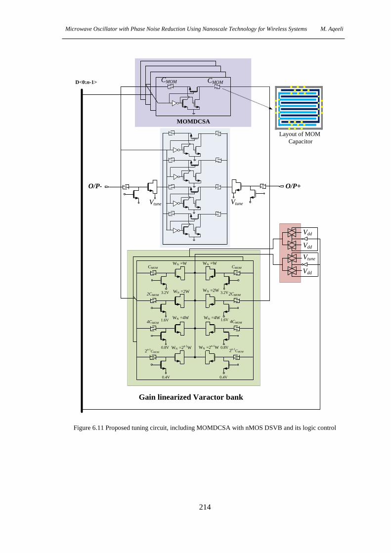
Microwave Oscillator with Phase Noise Reduction Using Nanoscale Technology for Wireless Systems M. Aqeeli
214
MOMDCSA
CMOM
O/P+O/P-
D<0:n-1>
Gain linearized Varactor bank
Layout of MOM
Capacitor
Vtune
CMOM
Vtune
CMOMCMOM
2CMOM2CMOM
Vtune
Vdd
Vdd
Vdd
WN =W
WN =2WWN =2W
WN =W
WN =2n-1WWN =2n-1W2n-1
CMOM2n-1CMOM
WN =4WWN =4W4CMOM 4CMOM
0.4V0.4V
3.2V3.2V
1.6V1.6V
0.8V0.8V
Figure 6.11 Proposed tuning circuit, including MOMDCSA with nMOS DSVB and its logic control

Microwave Oscillator with Phase Noise Reduction Using Nanoscale Technology for Wireless Systems M. Aqeeli
215
Table 6-5Working mode of the varactor bank
Group Binary Mode DC(4:3) Sub-bands
1 00 0-3
2 01 4-7
3 10 8-11
4 11 12-15
The proposed topology provides a relatively constant output swing frequency and
minimal phase noise over the operating frequency range. Thus, phase noise variations are
optimised. The DCSA capacitance value can be calculated as:
1
1 1 1(2 )N
MOM DF
CC C
(6.20)
where CMOM is the capacitance of the DCSA, and CDF is the drain fringe capacitance of
the switch devices. Total capacitance Cα of the series MOMDCSA, including fixed
parasitic capacitance of the active devices, PARC can be calculated as:
1
1 1(2 1)N
PAR
MOM DF
C CC C
(6.21)
where CDF is the drain fringe capacitance of the series MOMDCSA. Total capacitance Cβ
of the parallel MOMDCSA to the inductor and Cα is:
1
1 1(2 1)N
PAR
MOM DF
C CC C
(6.22)
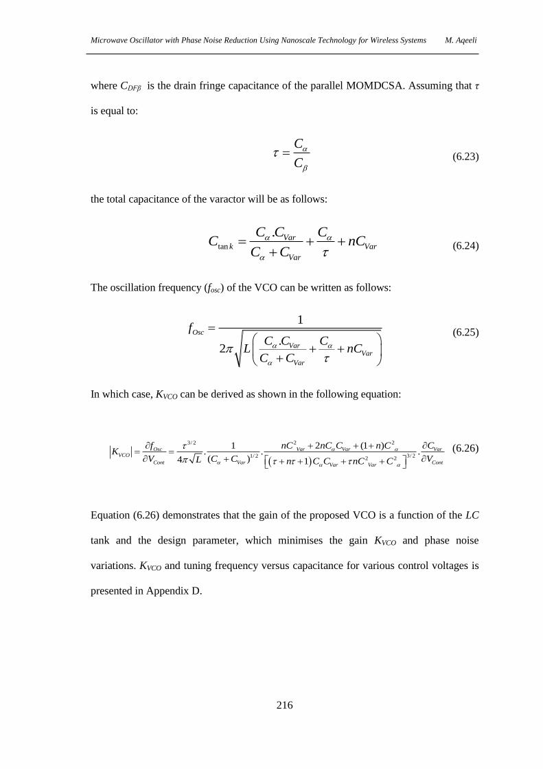
Microwave Oscillator with Phase Noise Reduction Using Nanoscale Technology for Wireless Systems M. Aqeeli
216
where CDFβ is the drain fringe capacitance of the parallel MOMDCSA. Assuming that τ
is equal to:
C
C
(6.23)
the total capacitance of the varactor will be as follows:
tan
. Vark Var
Var
C C CC nC
C C
(6.24)
The oscillation frequency (fosc) of the VCO can be written as follows:
1
.2
Osc
VarVar
Var
fC C C
L nCC C
(6.25)
In which case, KVCO can be derived as shown in the following equation:
2 23/ 2
3/ 21/ 2 2 2
2 (1 )1. . .( )4 1
Osc Var Var VarVCO
Cont Var ContVar Var
f nC nC C n C CK
V C C VL n C C nC C
(6.26)
Equation (6.26) demonstrates that the gain of the proposed VCO is a function of the LC
tank and the design parameter, which minimises the gain KVCO and phase noise
variations. KVCO and tuning frequency versus capacitance for various control voltages is
presented in Appendix D.
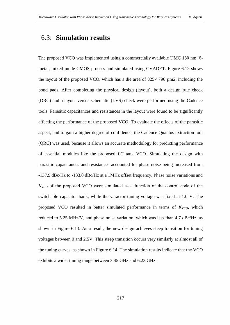
Microwave Oscillator with Phase Noise Reduction Using Nanoscale Technology for Wireless Systems M. Aqeeli
217
6.3: Simulation results
The proposed VCO was implemented using a commercially available UMC 130 nm, 6-
metal, mixed-mode CMOS process and simulated using CVADET. Figure 6.12 shows
the layout of the proposed VCO, which has a die area of 825× 796 µm2, including the
bond pads. After completing the physical design (layout), both a design rule check
(DRC) and a layout versus schematic (LVS) check were performed using the Cadence
tools. Parasitic capacitances and resistances in the layout were found to be significantly
affecting the performance of the proposed VCO. To evaluate the effects of the parasitic
aspect, and to gain a higher degree of confidence, the Cadence Quantus extraction tool
(QRC) was used, because it allows an accurate methodology for predicting performance
of essential modules like the proposed LC tank VCO. Simulating the design with
parasitic capacitances and resistances accounted for phase noise being increased from
-137.9 dBc/Hz to -133.8 dBc/Hz at a 1MHz offset frequency. Phase noise variations and
KVCO of the proposed VCO were simulated as a function of the control code of the
switchable capacitor bank, while the varactor tuning voltage was fixed at 1.0 V. The
proposed VCO resulted in better simulated performance in terms of KVCO, which
reduced to 5.25 MHz/V, and phase noise variation, which was less than 4.7 dBc/Hz, as
shown in Figure 6.13. As a result, the new design achieves steep transition for tuning
voltages between 0 and 2.5V. This steep transition occurs very similarly at almost all of
the tuning curves, as shown in Figure 6.14. The simulation results indicate that the VCO
exhibits a wider tuning range between 3.45 GHz and 6.23 GHz.

Microwave Oscillator with Phase Noise Reduction Using Nanoscale Technology for Wireless Systems M. Aqeeli
218
Th
e Varacto
r ban
k
Tran
smissio
n g
ateT
he
curr
ent
sou
rce
Th
e b
uff
er
Pro
po
sed V
CO
core
Th
e M
OM
DC
SA
Figure 6.12 Layout of the VCO with a die area of 720× 586 μm2
Microwave Oscillator with Phase Noise Reduction Using Nanoscale Technology for Wireless Systems M. Aqeeli
219
49.5
51.0
52.5
54.0
55.5
57.0
58.5
60.0
61.5
63.0
Kvco (MHz/V) Phase noise (dBc/Hz)
Coarse control code
Kvco@
1.0
V(M
Hz/V
)
-140
-135
-130
-125
-120
-115
-110
-105
-100
Pha
se
no
ise @
1.0
V(d
Bc/H
z)
5.2
5 M
Hz/
V
4.7
dB
c/H
z
0000 0001 0010 0011 0100 0101 0110 0111 1000 1001 1010 1011 1100 1101 1110 1111
Figure 6.13 KVCO and phase noise of the proposed VCO using MOMDCSA, an nMOS varactor pair and
DSVB as the functions of control codes
0.0 0.5 1.0 1.5 2.0 2.5
Oscill
atio
n f
req
ue
ncy(G
Hz)
Tuning voltage(V)
6.5
6.0
5.5
5.0
4.5
4.0
3.5
3.0
Figure 6.14 Oscillation frequency characteristics versus tuning voltage

Microwave Oscillator with Phase Noise Reduction Using Nanoscale Technology for Wireless Systems M. Aqeeli
220
The proposed VCO has good performance parameters, due mainly to the MOMDCSA
and the characteristics of the new design. Importantly, phase noise variations remain
relatively small for all tuning ranges, due to the advantages of the discrete frequency
ranges. Circuit performance, which was simulated using CVADET to show the transient
analysis of the VCO, demonstrates clearly that steady-state oscillation starts at
approximately 5.48 ns. The circuit generates stable periodic signals, with tuning
voltages varying from 0 to 2.5V. The FoM varies from -201.9 dBc/Hz to -204.6
dBc/Hz at a 1 MHz offset frequency, as shown in Figure 6.15, upon implementation of
the novel varactor.
-0.5 0.0 0.5 1.0 1.5 2.0 2.53.0
3.5
4.0
4.5
5.0
5.5
6.0
6.5
7.0
Oscilla
tio
n f
req
ue
ncy (
GH
z)
Tuning voltage - Frequency
Tuning voltage - FOM
Tuning voltage (V)
-180
-190
-200
-210
-220
-230
FO
M (
dB
c/H
z)
Figure 6.15 Tuning characteristics and FoM of the proposed VCO MOMDCSA in series and parallel to a
varactor with a gain-linearised DSVB varactor bank
As an illustration of the novel varactor’s usefulness, single sideband (SSB) phase noise
was simulated at a 1 MHz offset, while the carrier frequency was -133.8 dBc/Hz, as
shown in Figure 6.16. It is notable that phase noise is reduced by 1.7 dBc/Hz in the
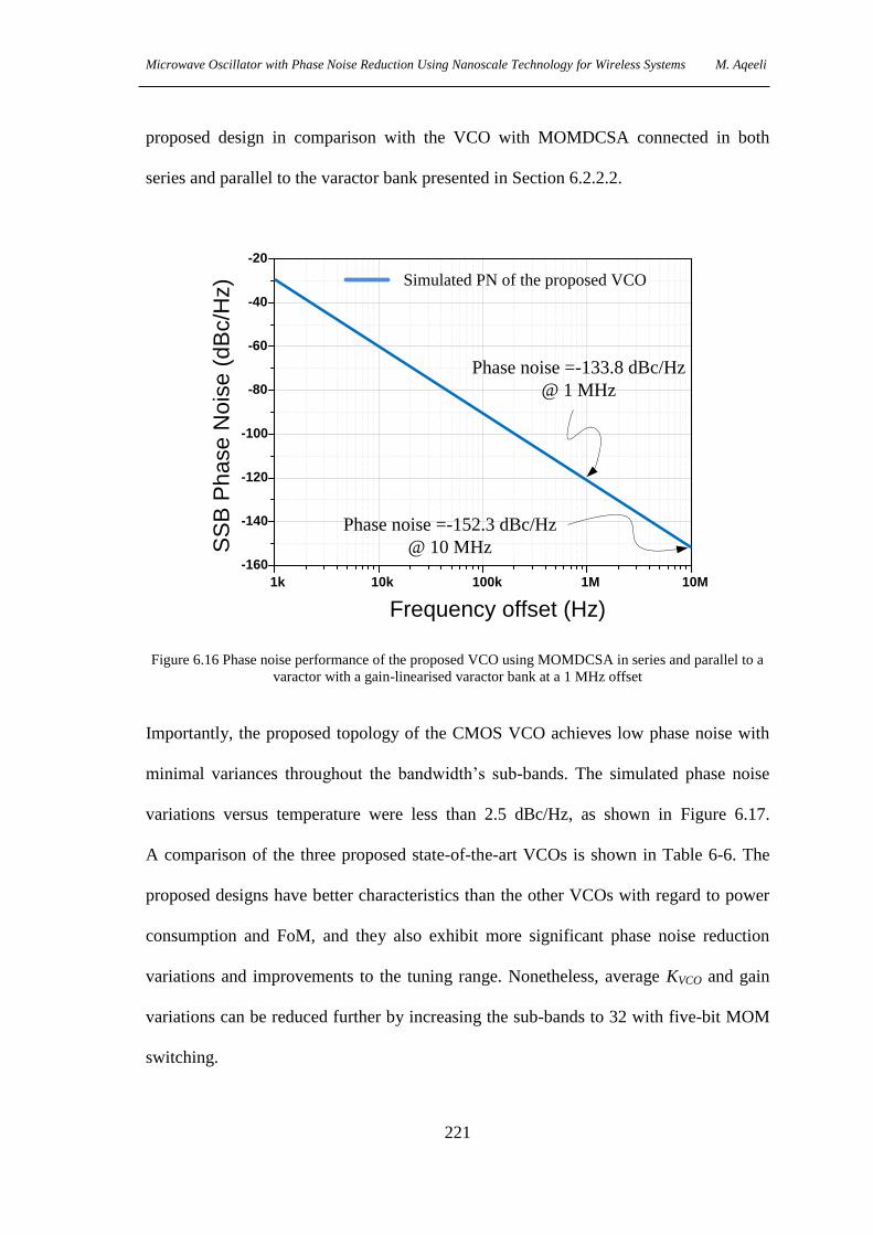
Microwave Oscillator with Phase Noise Reduction Using Nanoscale Technology for Wireless Systems M. Aqeeli
221
proposed design in comparison with the VCO with MOMDCSA connected in both
series and parallel to the varactor bank presented in Section 6.2.2.2.
1k 10k 100k 1M 10M
-160
-140
-120
-100
-80
-60
-40
-20
S
SB
Ph
ase
No
ise
(d
Bc/H
z)
Frequency offset (Hz)
Phase noise =-133.8 dBc/Hz
@ 1 MHz
Phase noise =-152.3 dBc/Hz
@ 10 MHz
Simulated PN of the proposed VCO
Figure 6.16 Phase noise performance of the proposed VCO using MOMDCSA in series and parallel to a
varactor with a gain-linearised varactor bank at a 1 MHz offset
Importantly, the proposed topology of the CMOS VCO achieves low phase noise with
minimal variances throughout the bandwidth’s sub-bands. The simulated phase noise
variations versus temperature were less than 2.5 dBc/Hz, as shown in Figure 6.17.
A comparison of the three proposed state-of-the-art VCOs is shown in Table 6-6. The
proposed designs have better characteristics than the other VCOs with regard to power
consumption and FoM, and they also exhibit more significant phase noise reduction
variations and improvements to the tuning range. Nonetheless, average KVCO and gain
variations can be reduced further by increasing the sub-bands to 32 with five-bit MOM
switching.

Microwave Oscillator with Phase Noise Reduction Using Nanoscale Technology for Wireless Systems M. Aqeeli
222
-40 -20 0 20 40 60 80 100 120 140
-134.0
-133.5
-133.0
-132.5
-132.0
-131.5
-131.0P
ha
se
no
ise
(d
Bc/H
z)
Temperature (oC)
Phase noise against temperature
< 2
.5 d
Bc/
Hz
Figure 6.17 Phase noise variation against temperature in degrees Celsius (°C)
Table 6-6 A comparison between the three proposed VCOs
Parameter
B
C
D
PN Variances (dBc/Hz) ∼12.7 ∼4.9 ∼4.68
PN at Centre Frequency (dBc/Hz) -133.40 -132.7 -133.8
FoM@1MHz Offset(dBc/Hz) -203.3 -201.9 -203.5
Tuning Range (GHz) 4.45-5.43 3.45-5.78 3.45-6.23
KVCO Variation (MHz/V) 23.5 5.7 5.25
Spurious harmonics (dBm) 32 35 41
Power Consumption (mW) 2.9 2.88 3.2
A: MOMDCSA in parallel to gain linearised nMOS varactor bank [25]
B: MOMDCSA in series and parallel to nMOS varactor bank [84]
C: MOMDCSA in series and parallel to nMOS varactor with gain linearised bank [14, 84, 85]
PN: Phase Noise
Microwave Oscillator with Phase Noise Reduction Using Nanoscale Technology for Wireless Systems M. Aqeeli
223
6.4: Chapter summary
Phase noise performance is directly proportional to gain, KVCO. As a consequence, a
large KVCO will amplify any noise coupling to the control node and therefore degrade
phase noise performance. This problem is not as widely acknowledged in the literature
as perhaps it might be. As indicated in Chapter one, the main objective of this study is
to present a novel VCO design that can provide low phase noise variation, a wide tuning
range, a competitive FoM, a compact size and low power consumption and performance
enhancement. Phase noise varies dramatically over the tuning range of a VCO. High Q
factor varactors have regularly narrower tuning ranges, and as a result, the reduction of
phase noise at a certain frequency as well as phase noise variations commonly reveal
undesirable manufacturing errors. Standard CMOS technology offers diodes and MOS
capacitors as varactors. nMOS in accumulation-mode and pMOS in inversion-mode
varactors can provide significant VCO tuning ranges; however, Q factor variations close
to the VTH cause phase noise in the LC-VCO to fluctuate dramatically in line with the
control voltage. Consequently, it is difficult to attain a large tuning range and small
phase noise variations simultaneously, by accommodating MOS varactors, because it
increases the probability of converting AM noise to FM noise. This will expand in line
with differences between the maximum and the minimum capacitances, and it may
become indistinguishable from phase noise. Thus, switching capacitors are mandatory
when seeking to maintain minimum phase noise variations for wide tuning ranges and
low VCO sensitivity, KVCO. Many researches which consider switching capacitors inside
the LC tank, in order to extend the tuning range and minimise VCO phase noise.
However, their studies result in occupying a larger die area as well as exhibiting large
phase noise variations and higher power dissipation. For low phase noise, it is necessary

Microwave Oscillator with Phase Noise Reduction Using Nanoscale Technology for Wireless Systems M. Aqeeli
224
to have as small KVCO as possible. However, this smaller KVCO creates a narrow
frequency locking range. In some designs phase noise variations exceed 25 dB. In a
wide tuning range, variations between the minimum and the maximum values of the
frequencies (fmax-fmin) will be large, meaning large variations for KVCO. As proof of this
theory, and to compare the studies presented in this thesis, a pMOS-only VCO design
with body-bias varactors, presented in several works, was constructed and simulated.
The results show clearly the existence of significant phase noise variations. Therefore,
this thesis presents a solution to this problem and a trade-off between the frequency
tuning range and KVCO variations.
Three different wideband LC-VCOs have been designed and simulated using a UMC-
130nm mixed-mode CMOS process for high performance. An ideal VCO, utilising an
MOMDCSA, an nMOS varactor pair and a DSVB, has been employed, along with an
achieved broadband tuning range, which varies linearly with the control voltage.
It can be concluded that the proposed VCO with MOMDCSA connected both in series
and parallel to a varactor with a gain-linearised varactor bank has better characterisation
over other switches and a more significant effect on phase noise reduction variations.
After completing the physical design (layout), both a design rule check (DRC) and a
layout versus schematic (LVS) check were performed using Cadence tools. Parasitic
capacitances and resistances in the layout were found to be significantly affecting the
performance of the proposed VCO. To evaluate the effects of this parasitic element, and
to gain a higher degree of confidence, the QRC tool was used, because it provides a
convenient and accurate methodology to predict performance in critical building blocks
such the proposed LC tank VCO. Simulating the design with parasitic capacitances and
Microwave Oscillator with Phase Noise Reduction Using Nanoscale Technology for Wireless Systems M. Aqeeli
225
resistances accounted for phase noise being increased from -136.9 dBc/Hz
to -133.8 dBc/Hz at a 1MHz offset frequency.
Phase noise variations and the gain of the proposed VCO were simulated as a function
of the control code of the switchable capacitor bank, while the varactor tuning voltage
was fixed at 1.0 V. The proposed VCO resulted in better simulated performance in
terms of KVCO, which reduced to 5.25 MHz/V, and phase noise variation, which was less
than 4.7 dBc/Hz. As a result, the new design achieves a steep transition for tuning
voltages varying between 0 and 2.5V. This steep transition occurs similarly for almost
all of the tuning curves. High-performance VCO specifications include measured phase
noise of -133.8 dBc/Hz at an offset frequency of 1 MHz away from a 5.0 GHz FoM of -
203.5 dBc/Hz, while the VCO core’s total power consumption is 3.2 mW, using a 1.2V
supply voltage. The output peak-to-peak voltage of the VCO is 2.6V, with excellent
spurious harmonics at < 41 dBm. For CMOS, there are currently no published VCO
designs featuring this topology, its performance or specifications. As proof of the
concept, the performance of the novel VCO in this study is compared in Table 6-7 to
other state-of-the-art designs in 0.09 µm, 0.13 μm and 0.18 μm CMOS technologies. A
wideband LC VCO is designed in TSMC 0.13-µm CMOS process is presented in [52] .
Bias filters are used to suppress the dynamic transient effects and the reference current
noise on the bias line.

Microwave Oscillator with Phase Noise Reduction Using Nanoscale Technology for Wireless Systems M. Aqeeli
226
Table 6-7 Performance comparison of CMOS VCOs
Process
CMOS
F
(GHz)
P
(mW)
PN
(dBc/Hz)
Offset
(MHz)
TR
(GHz)
FoM
(dBc/Hz)
Ref.
0.18µm 4.20 4.5 -119.0 1.0 4.1-4.8 -184.5 [52] S
0.18µm 5.00 7.2 -90.2 1.0 4.1-5.0 -154.8 [72]
0.65nm 3.30 5.0 -137.4 3.0 3.0-4.5 186.5 [74]
0.65nm 4.35 41.6 144.8 3.0 3.6-4.4 -197.4 [86]
0.13µm 4.80 10.1 -126.1 1.0 4.0-4.8 -189.6 [87]
0.18µm 5.20 1.8 -119.9 1.0 5.2-6.3 -191.7 [88]
0.18µm 5.00 13.0 -121.5 1.0 5.1-5.4 -192.1 [89]
0.18µm 3.50 8.8 -125.9 1.0 3.1-3.9 -191.7 [90]
0.09µm 3.95 6.6 -147.0 10.0* 3.4-4.5 -191.0 [91]
0.13µm 5.00 3.2 -133.8 1.0 3.5-6.2 -203.5 This work
F: Centre frequency, P: power, PN: Phase noise, TR: Tuning range
The performance of the proposed VCO performs the tuning range of 3.14-3.88 GHz and
3.86-5.28 GHz and phase noise of around -119 dBc/Hz at 1.0 MHz offset frequency
over the whole working band, the current consumption is less than 4.5 mA from 1.2V
power supply. [72] Presents a new gain linearized varactor bank for wideband VCOs.
The design is fabricated in a 0.18-μm CMOS technology. The VCO tuning gain
linearized techniques, namely the gain variation compensation and linear tuning range
extension techniques, are used in the proposed varactor bank to achieve a further
reduced VCO tuning gain with low variation. Fabricated in a 0.18-μm CMOS
technology, a 3-bits VCO prototype employing the proposed varactor bank achieves
<5% gain variation at the output frequency from 4.1 to 5 GHz, and exhibits maximum
power consumption of 7.2 mW at its peak frequency, 5 GHz. In [74] a low core
current-VCO for multi-standard cellular transceivers is fabricated in a 65-nm CMOS
process. If the core current is large, a VCO with a smaller core-size can lower phase

Microwave Oscillator with Phase Noise Reduction Using Nanoscale Technology for Wireless Systems M. Aqeeli
227
noise. Based on the analysis, the effective core-size of the VCO is designed to be
scalable according to the core current, by switching the secondary core-transistors on or
off. Thus, the proposed VCO becomes adaptive to multi-standard cellular transceivers.
When the core current is set to 4 mA, the VCO in the LP mode achieved the phase noise
of 127.9 dBc/Hz at the 3 MHz offset from 3.3-GHz signals. When the core current is set
to 15 mA, phase noise of the VCO in the LN mode is minimized to 137.5 dBc/Hz at the
same offset. The FoM is 184.8 and 186.5 dB, respectively.
In [86] a new class of operation of an RF oscillator that minimizes its phase noise is
presented. The main idea is to enforce a clipped voltage waveform around the LC tank
by increasing the second-harmonic of fundamental oscillation voltage through an
additional impedance peak, thus giving rise to a class-F2 operation. As a result, the
noise contribution of the tail current transistor on the total phase noise can be
significantly decreased without sacrificing the oscillator's voltage and current
efficiencies. Furthermore, its special impulse sensitivity function (ISF) reduces the
phase sensitivity to thermal circuit noise. The prototype of the class-F2 oscillator is
implemented in standard TSMC 65 nm CMOS occupying 0.2 mm2. It draws 32–38 mA
from 1.3 V supply. Its tuning range is 19% covering 7.2–8.8 GHz. It exhibits phase
noise of 139 dBc/Hz at 3 MHz offset from 8.7 GHz carrier, translated to an average
figure-of-merit of 191 dBc/Hz with less than 2 dB variation across the tuning range. The
long term reliability is also investigated with estimated >10 year lifetime.
In [87] VCO design method for extended tuning range with low phase noise is applied
and verified by simulations, implementation and measurements on 130-nm CMOS. The
oscillator tuning range is expanded from 49.4% to 60.2% by shorting transformer
Microwave Oscillator with Phase Noise Reduction Using Nanoscale Technology for Wireless Systems M. Aqeeli
228
secondary winding with a switch. The VCO achieved a phase noise between
-123.4dBc/Hz and -126.1dBc/Hz at a 1 MHz offset covering bandwidth ranges from a
4.0 GHz and 4.8 GHz carrier while consuming less than 7.5 mA from 1.8 V power
supply. In [88] a linear KVCO dual-tuning CMOS VCO has been proposed and
implemented in the TSMC IP6M micrometer CMOS process. The dual tuning varactor
and the tail transistor structure could extend the bandwidth phase noise and power
consumption. The KVCO exhibits 150MHz/V from 5.2 GHz to 6.3 GHz with 19% tuning
ratio. The phase noise is -119.9dBc/Hz at 1MHz offset frequency. The power
consumption is 1.8mW from 1.4V supply.
In [89] a fully integrated CMOS LC VCO is presented which exhibits low phase noise
and low power consumption. To reduce the phase noise, the researchers used a bias
filter consisting of an inductor and capacitor to suppress noise. In addition, the source of
tail current uses a memory reduced tail transistor to avoid degradation of phase noise
and to gain low power consumption. The prposed VCO is designed and implemented by
0.18-µm TSMC CMOS process and achieves -100.9 and -121.5 dBc/Hz at 1 kHz and 1
MHz offsets respectively. The current consumption is 1.5mA with a 1.5V power supply.
A figure-of-merit of -192.1 dBc/Hz is observed by simulation.
A dual-band wide-tuning-range quadrature (Q) VCO using a harmonic-injection
coupling technique is proposed in [90]. The tuning range of a switched capacitor and a
switched-inductor LC-tank are investigated. Based on the investigation, a switched-
inductor tank is employed since it provides a wide tuning range. A harmonic injection
coupling technique, which eliminates the noise sources of coupling transistors, is
Microwave Oscillator with Phase Noise Reduction Using Nanoscale Technology for Wireless Systems M. Aqeeli
229
applied to generate the quadrature outputs. The QVCO is designed for 3.5GHz WiMAX
and 2.4 GHz ISM applications. Theses achieve a tuning range of 24.9% and 20.7%,
measured phase noise of -123.5 dBc/Hz and -125.9 dBc/Hz at a 1MHz offset and FoM
of -191.7 and -192.4 respectively.
Work presented in [91] shows two class-C CMOS VCOs with a dynamic bias of the
core transistors, which maximizes the oscillation amplitude without compromising the
robustness of the oscillation start-up, thereby breaking the most severe trade-off in the
original class-C topology. An analysis of several different oscillators, starting with the
common class-B architecture and arriving to the proposed class-C design, shows that
the latter exhibits FoM that is closest to the ideal FoM allowed by the integration
technology. The class-C VCOs have been implemented in a 90 nm CMOS process with
a thick top metal layer. They are tunable between 3.4 GHz and 4.5 GHz, covering a
tuning range of 28%. Drawing 5.5 mA from 1.2 V, the phase noise is lower than 152
dBc/Hz at a 20 MHz offset from a 4 GHz carrier. The resulting FoM is 191 dBc/Hz, and
varies by less than 1 dB across the tuning range.
The results show clearly that the presented VCO with MOMDCSA in series and
parallel to a varactor with gain linearized varctor bank is the best in terms of phase
noise, power dissipation, bandwidth and FoM, not only for fabricated work but also for
simulated designs as well. The simulation results indicate that the VCO exhibits a wider
tuning range between 3.45 GHz and 6.23 GHz, at approximately 56%. Phase noise
variations range from -135.67 dBc/Hz to -130.97 dBc/Hz, and the FoM varies from -
202.1 dBc/Hz to -204.5 dBc/Hz at a 1 MHz offset frequency. Circuit performance,
which is simulated using CVADET to show the transient analysis of the VCO,
demonstrates clearly that steady-state oscillation starts at approximately 5.48 ns. The

Microwave Oscillator with Phase Noise Reduction Using Nanoscale Technology for Wireless Systems M. Aqeeli
230
three proposed VCOs can be implemented widely in 5GHz Wireless LANs in industrial
and in WLAN radio applications [92]. Better coverage and higher WLAN capacity have
resulted in increasing requirements for Worldwide Interoperability for Microwave
Access (WiMAX) technology. The IEEE’s unlicensed national information
infrastructure WiMAX band (as specified by IEEE 802.16) provides both fixed and
portable wireless broadband connectivity, independent of a base station [93, 94]. The
majority of countries around the world have embraced the 5 GHz spectrum for licence-
exempt communications. IEEE 802.11a radio also utilises the 5GHz frequency band
(5.180 – 5.825GHz).
Microwave Oscillator with Phase Noise Reduction Using Nanoscale Technology for Wireless Systems M. Aqeeli
231
Low Phase Noise Chapter 7:
Microwave Oscillator Based
on a Miniaturised Meta-
material Bandpass Filter
At the beginning of the century and the start of the new millennium, a new research
field appeared in the fields of science and technology: metamaterials. Indeed, the
number of journal and conference papers, special sessions in conferences and research
and development projects and contracts related to metamaterials has experienced
exponential growth since 2000. Metamaterials can be considered a transversal topic,
involving many different disciplines and fields, such as acoustics, electromagnetism, RF
and microwave engineering, millimetre wave and THz technology, micro- and
nanotechnology, photonics and optics and medical engineering, among others. During
the last few years, several books devoted to metamaterials have been published by

Microwave Oscillator with Phase Noise Reduction Using Nanoscale Technology for Wireless Systems M. Aqeeli
232
active researchers in the field [95-97]. Such books cover different aspects of
metamaterial science and technology, including theory, technology and applications. In
this chapter, the focus is on the applications and the implementation of metamaterial
concepts in the design of RF/microwave devices for wireless applications.
Metamaterials are synthetic materials manufactured from periodic particles of
conventional ingredients with controllable electromagnetic properties [95]. In these
artificial materials, the period is considerably smaller than the guided wavelength;
therefore, the structure behaves as a homogeneous medium, exhibiting effective
medium properties. Such properties can be controlled by properly engineering the
material, and they can be substantially different to those observed in conventional
transmission lines. For instance, it was experimentally demonstrated in [98] that a prism
made of metallic strips and split ring resonators etched on dielectric slabs exhibits a
negative refractive index in a defined frequency band. Indeed, such artificial media,
with negative permittivity and permeability, exhibit not only negative refraction, but
also backward waves, an inverse Doppler effect and backward Cerenkov radiation [95].
Such properties were already predicted by Veselago in 1968, but it was not until the
past decade that such properties were experimentally demonstrated.
The first reported bulk structure exhibiting negative permittivity and permeability was
published in 2000 by the Smith Group [99]. The structure consisted of an array of
metallic posts and SRRs. The array of metallic posts behaves like an effective medium,
which has negative permittivity below a frequency, that is controlled by the posts’
radius and the distance between them, while the SRRs exhibit negative effective
permeability in a narrow band above their resonance frequency. Thus, by designing the
SRRs in order to present their first resonance in the negative permittivity region of the
Microwave Oscillator with Phase Noise Reduction Using Nanoscale Technology for Wireless Systems M. Aqeeli
233
posts, the combined post and SRR structure exhibits negative constitutive parameters in
a specified narrow band. However, the structure is highly anisotropic, since it is
necessary to excite it with an electrical field parallel to the posts and a magnetic field
axial to the SRRs. From Maxwell’s equations, it can be demonstrated easily that a
structure with negative permeability and permittivity supports backward waves [100].
Namely, in such media, group velocity and phase velocity are anti-parallel. The wave
vector, the magnetic field vector and the electrical field intensity vector form a left-
handed triplet, and so for this reason such materials have been called ‘left-handed’ (LH)
materials. In RF and microwave engineering, the constitutive components are
transmission lines and stubs. As long as metamaterials exhibit properties beyond those
achievable with conventional materials, it is possible to load a transmission line with
reactive elements, in order to obtain properties not present in conventional lines.
The properties and the specifications of LH metamaterials, demonstrated in
[101-105] through full-wave analysis, show some signs of future success for a diverse
range of microwave and optical applications, such as new types of bandpass filters,
super-lenses, modulators, microwave components and sophisticated antennas. On the
other hand, the LH structures offered at first were unwieldy for microwave applications,
because of their narrow bandwidth characteristics and the fact that they were too lossy.
Alternative theories seem to be very attractive in relation to obtaining a deep and
intuitive understanding of their behaviour.
A low phase noise oscillator is presented in this chapter based on an LH metamaterial
bandpass filter. The idea of using an LH metamaterial filter to design an oscillator was
first introduced in [106], and there have been a number of notable published works by a
Microwave Oscillator with Phase Noise Reduction Using Nanoscale Technology for Wireless Systems M. Aqeeli
234
group at University of Manchester [104, 107], in which different novel metamaterial
concepts have been verified independently.
In the microwave frequency range, standard CMOS LC-tank oscillators are preferred
for their compact size and excellent phase noise performance. However, the cost of this
fabrication is expensive. A novel oscillator operating at 2.0 GHz, based on miniaturised
metamaterial bandpass filters with low phase noise, is presented in his chapter. In the
proposed oscillator design, the passband filter is embedded in the feedback loop, to be
used as a frequency stabilisation element [102].
The peak frequency of the complex quality factor Qsc of the miniaturised filter is
adopted in this project to design the proposed oscillator as a substitution for the group-
delay-peak frequency. To prove the effectiveness of the proposed concept, two filter-
based oscillators were designed and simulated using Computer Simulation Technology
(CST). The first was designed at the Qsc-peak frequency, while in the second one the
group-delay-peak frequency was used. It was found that the first oscillator achieved
excellent phase noise and was improved by more than 10 dB compared to the group-
delay-peak frequency oscillator. The improvement was verified experimentally. The
measured phase noise was 152.1 dBc/Hz at a 1 MHz offset frequency.
7.1: Introduction to CST
CST is a particularistic tool for the three-dimensional (3D) electromagnetic (EM)
simulation of high-frequency components [108]. CST’s performance and capabilities
make it the first choice for many researchers in universities around the world as well as
research and development engineers in the industry. It enables the fast and accurate
design of high-frequency devices such as filters, absorbers, antennas, couplers, planar
Microwave Oscillator with Phase Noise Reduction Using Nanoscale Technology for Wireless Systems M. Aqeeli
235
and multi-layer structures, and it is fast software which gives an insight into the EM
behaviour of high-frequency structures. Furthermore, it offers users great flexibility in
designing a wide application range through different solver technologies such as time
domains and frequency domain solvers. In addition, CST can be used with several
industry-standard workflows through its user interface.
The accuracy of two well-known solvers in the CST microwave studio, the time and
frequency domains, are improved by using the exemplary boundary approximation
(PBA) [109], thin sheet technique (TST), and true geometry adaptation. PBA is
considered an extension of the finite integration theory, in which very complicated 3D
cavities can be modelled efficiently. Also, the PBA technique reduces solver simulation
time by one order of magnitude compared to the conventional method for structures
with many curved boundaries. This technique was used in CST to model an input
coupler for TESLA superconducting cavities, where a rounded transition was needed
between rectangular and an elliptical waveguide [109]. The S-parameter simulation
results show a reflection of more than -40 dB in the design frequency of 1.3 GHz. TST
improves the accuracy of the solver by independently treating two of two dielectric
parts of a mesh cell, separated by a metallic sheet. The combination of these techniques
increases CST computational performance and accuracy.
7.2: Fundamentals of left-handed metamaterials
Electromagnetic metamaterials (MTM) are artificial electromagnetic structures with
exceptional properties not readily found in nature [100]. The structural average value of
cell size p must be at least smaller than a quarter of the guided wavelength λg to meet
the effective homogeneity condition. This condition ensures that refraction dominates

Microwave Oscillator with Phase Noise Reduction Using Nanoscale Technology for Wireless Systems M. Aqeeli
236
scattering or diffraction for reliable wave propagation inside MTM media. When this
condition is met, the structure can be seen as a material with constitutive parameters of
electric permittivity ε and permeability µ, where it is electromagnetically uniform across
the propagation direction. The refractive index n is realised in terms of the constitutive
parameters ε and µ as:
r rn (7.1)
where 𝜇𝑟 𝑎𝑛𝑑 휀𝑟 are permeability and relative permittivity, respectively, which are
associated with free space permeability and permittivity by 휀0 =ε
ε𝑟= 8.854 × 10⁻¹²
and 𝜇𝑜 =µ
𝜇𝑟= 4𝜋 × 10−7. It can be concluded from (7.1) that the sign for (ε, µ) can be
(+,+), (+,-), (-,+) and (-,-), as shown in Figure 7.1. The first quadrant of the ε- µ diagram
corresponds to the conventional right-handed material with forward wave propagation.
When either ε or µ is less than zero, the wave cannot propagate, because the negative
sign for either ε or µ results in an imaginary propagation constant β=nk0= ±√휀𝑟𝜇𝑟 and
a stopband can be observed. The fourth quadrant in Figure 7.1 represents left-handed
(LH) material where ε and µ are simultaneously negative. Such materials can be
identified by anti-parallel phase and group velocities because of their double-negative
parameters.
In 1967, Viktor Veselago predicted the existence of an LH MTM that would allow
backward wave propagation [110]. This prediction was confirmed three decades later by
Smith, who proposed a structure consisting of continuous thin wires and split ring
resonators, arranged in a periodic structure, as shown in Figure 7.2, which allow wave
propagation at a certain frequency region with negative-ε and negative-µ [111].
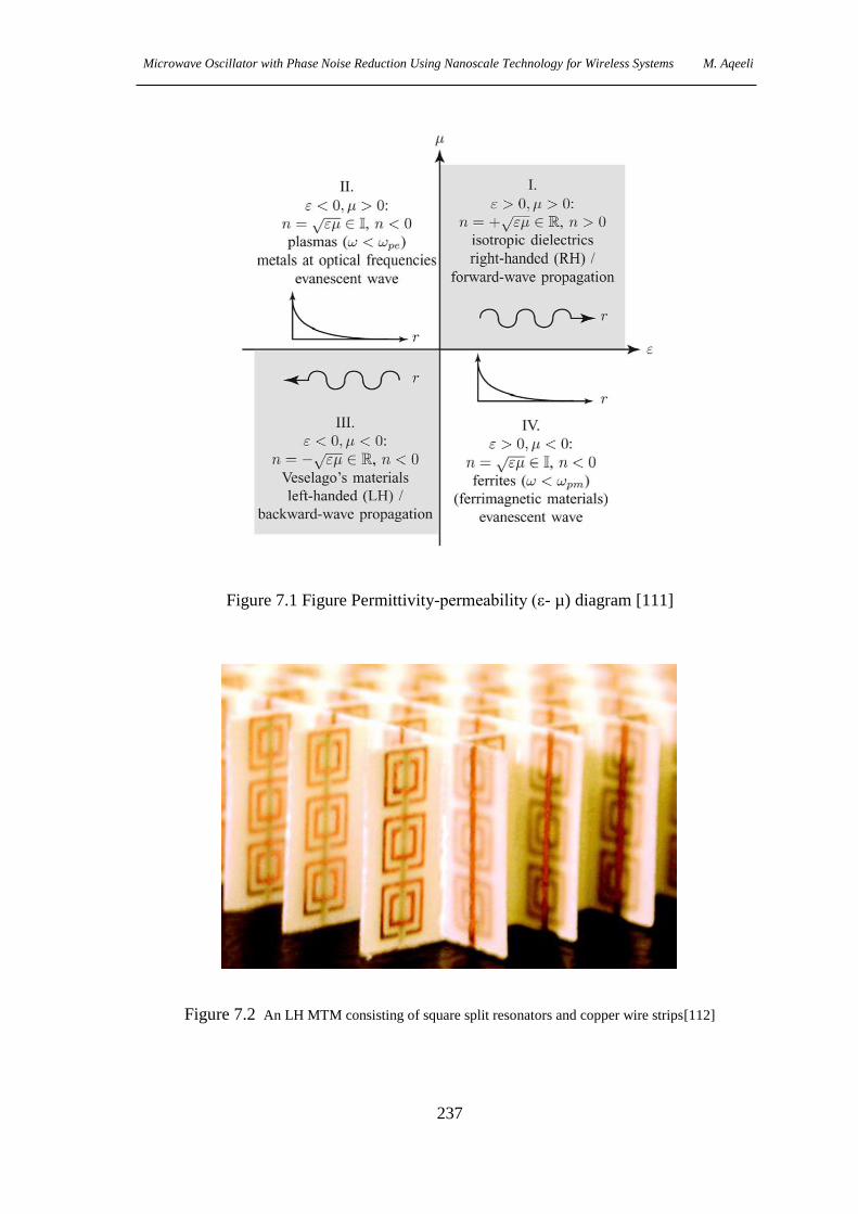
Microwave Oscillator with Phase Noise Reduction Using Nanoscale Technology for Wireless Systems M. Aqeeli
237
Figure 7.1 Figure Permittivity-permeability (ε- µ) diagram [111]
Figure 7.2 An LH MTM consisting of square split resonators and copper wire strips[112]

Microwave Oscillator with Phase Noise Reduction Using Nanoscale Technology for Wireless Systems M. Aqeeli
238
After Smith’s breakthrough, research on LH MTMs continued, and different theoretical
and experimental approaches were used to verify backward wave propagation. The LH
structure presented in Figure 7.2 was inspired by Pendry’s work in [101] and can be
considered as a resonant type of structure that suffers from high loss and exhibits
narrow bandwidth. Therefore, the transmission line approach of MTM was presented by
Caloz in [100], to solve the problems of the resonant type of structure presented by
Smith. In the next section, it will be shown that the TL approach of MTM is preferred,
since classical TL theory can be used to design and analyse an LH MTM.
7.3: Transmission line approach
The main characteristic of the LH TL is its anti-parallel phase and group velocities,
which can be easily verified when considering the incremental circuit model for a
lossless LH TL, as shown in Figure 7.3.
' '1 ( )LZ j C
' '1 ( )LZ j L
' ( . )LC F m
0z
' ( . )LL H m
Figure 7.3 The “incremental circuit model for a hypothetical uniform LH TL”[95]
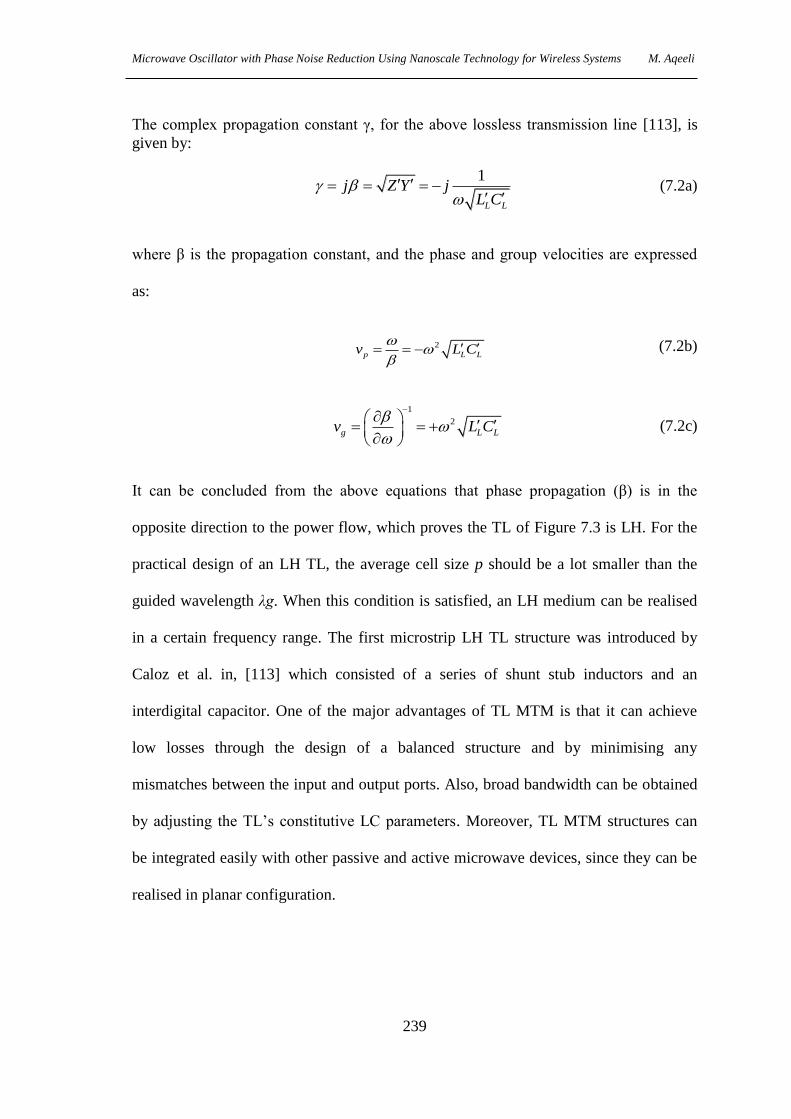
Microwave Oscillator with Phase Noise Reduction Using Nanoscale Technology for Wireless Systems M. Aqeeli
239
The complex propagation constant γ, for the above lossless transmission line [113], is
given by:
1
L L
j Z Y jL C
(7.2a)
where β is the propagation constant, and the phase and group velocities are expressed
as:
2
p L Lv L C
(7.2b)
1
2
g L Lv L C
(7.2c)
It can be concluded from the above equations that phase propagation (β) is in the
opposite direction to the power flow, which proves the TL of Figure 7.3 is LH. For the
practical design of an LH TL, the average cell size p should be a lot smaller than the
guided wavelength λg. When this condition is satisfied, an LH medium can be realised
in a certain frequency range. The first microstrip LH TL structure was introduced by
Caloz et al. in, [113] which consisted of a series of shunt stub inductors and an
interdigital capacitor. One of the major advantages of TL MTM is that it can achieve
low losses through the design of a balanced structure and by minimising any
mismatches between the input and output ports. Also, broad bandwidth can be obtained
by adjusting the TL’s constitutive LC parameters. Moreover, TL MTM structures can
be integrated easily with other passive and active microwave devices, since they can be
realised in planar configuration.
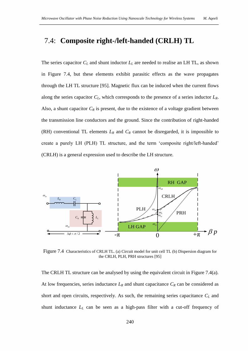
Microwave Oscillator with Phase Noise Reduction Using Nanoscale Technology for Wireless Systems M. Aqeeli
240
7.4: Composite right-/left-handed (CRLH) TL
The series capacitor CL and shunt inductor LL are needed to realise an LH TL, as shown
in Figure 7.4, but these elements exhibit parasitic effects as the wave propagates
through the LH TL structure [95]. Magnetic flux can be induced when the current flows
along the series capacitor CL, which corresponds to the presence of a series inductor LR.
Also, a shunt capacitor CR is present, due to the existence of a voltage gradient between
the transmission line conductors and the ground. Since the contribution of right-handed
(RH) conventional TL elements LR and CR cannot be disregarded, it is impossible to
create a purely LH (PLH) TL structure, and the term ‘composite right/left-handed’
(CRLH) is a general expression used to describe the LH structure.
RH GAP
LH GAP
cR
sh
se
cL
0
p
PLHPRH
CRLH
+π 0-π / 2
RL LC
LLRC
se
sh
Figure 7.4 Characteristics of CRLH TL. (a) Circuit model for unit cell TL (b) Dispersion diagram for
the CRLH, PLH, PRH structures [95]
The CRLH TL structure can be analysed by using the equivalent circuit in Figure 7.4(a).
At low frequencies, series inductance LR and shunt capacitance CR can be considered as
short and open circuits, respectively. As such, the remaining series capacitance CL and
shunt inductance LL can be seen as a high-pass filter with a cut-off frequency of
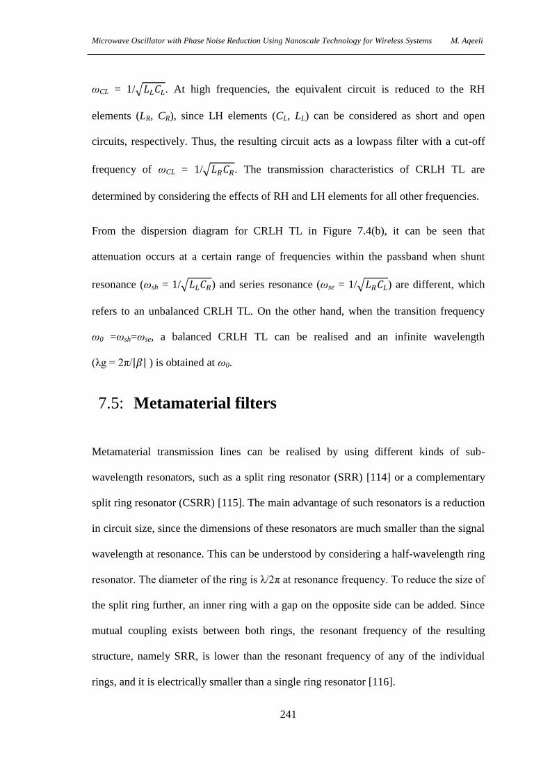
Microwave Oscillator with Phase Noise Reduction Using Nanoscale Technology for Wireless Systems M. Aqeeli
241
ωCL = 1/√𝐿𝐿𝐶𝐿. At high frequencies, the equivalent circuit is reduced to the RH
elements (LR, CR), since LH elements (CL, LL) can be considered as short and open
circuits, respectively. Thus, the resulting circuit acts as a lowpass filter with a cut-off
frequency of ωCL = 1/√𝐿𝑅𝐶𝑅. The transmission characteristics of CRLH TL are
determined by considering the effects of RH and LH elements for all other frequencies.
From the dispersion diagram for CRLH TL in Figure 7.4(b), it can be seen that
attenuation occurs at a certain range of frequencies within the passband when shunt
resonance (ωsh = 1/√𝐿𝐿𝐶𝑅) and series resonance (ωse = 1/√𝐿𝑅𝐶𝐿) are different, which
refers to an unbalanced CRLH TL. On the other hand, when the transition frequency
ω0 =ωsh=ωse, a balanced CRLH TL can be realised and an infinite wavelength
(λg = 2π/|𝛽| ) is obtained at ω0.
7.5: Metamaterial filters
Metamaterial transmission lines can be realised by using different kinds of sub-
wavelength resonators, such as a split ring resonator (SRR) [114] or a complementary
split ring resonator (CSRR) [115]. The main advantage of such resonators is a reduction
in circuit size, since the dimensions of these resonators are much smaller than the signal
wavelength at resonance. This can be understood by considering a half-wavelength ring
resonator. The diameter of the ring is λ/2π at resonance frequency. To reduce the size of
the split ring further, an inner ring with a gap on the opposite side can be added. Since
mutual coupling exists between both rings, the resonant frequency of the resulting
structure, namely SRR, is lower than the resonant frequency of any of the individual
rings, and it is electrically smaller than a single ring resonator [116].
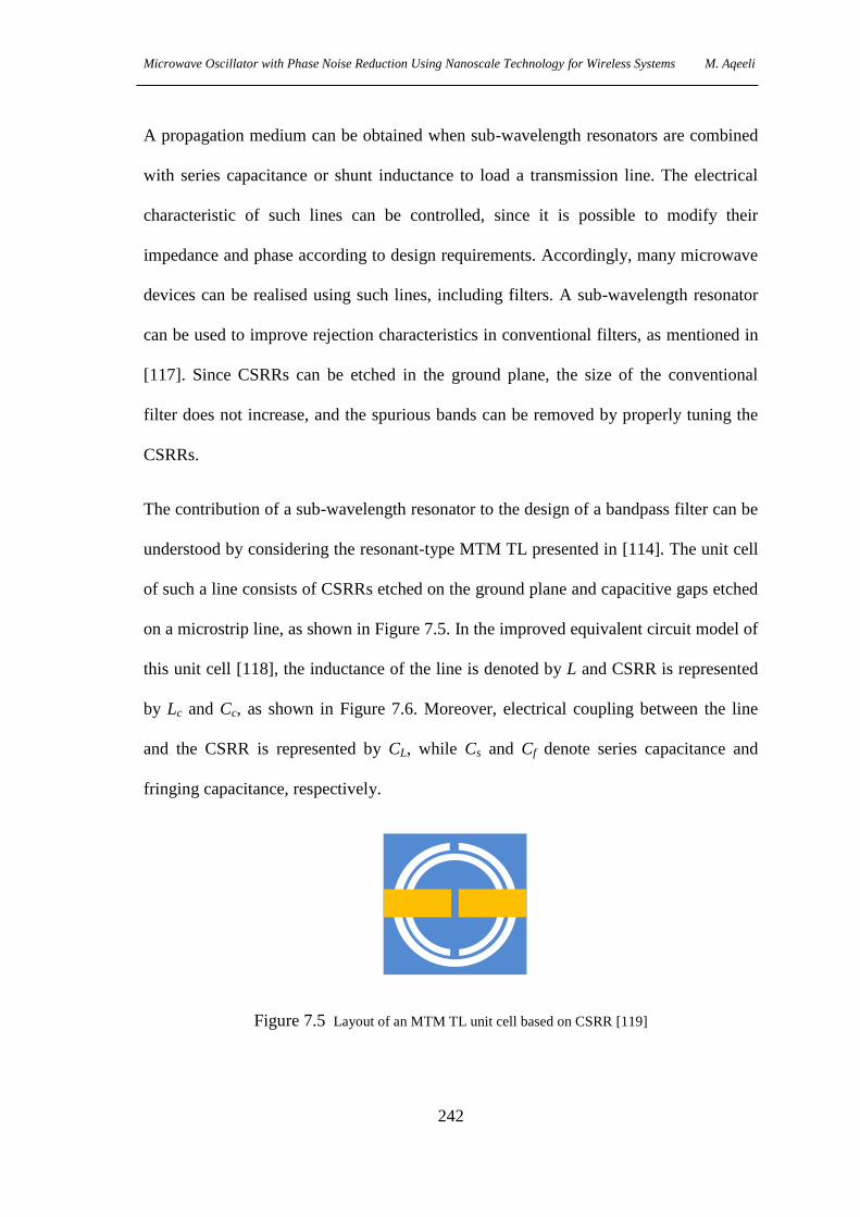
Microwave Oscillator with Phase Noise Reduction Using Nanoscale Technology for Wireless Systems M. Aqeeli
242
A propagation medium can be obtained when sub-wavelength resonators are combined
with series capacitance or shunt inductance to load a transmission line. The electrical
characteristic of such lines can be controlled, since it is possible to modify their
impedance and phase according to design requirements. Accordingly, many microwave
devices can be realised using such lines, including filters. A sub-wavelength resonator
can be used to improve rejection characteristics in conventional filters, as mentioned in
[117]. Since CSRRs can be etched in the ground plane, the size of the conventional
filter does not increase, and the spurious bands can be removed by properly tuning the
CSRRs.
The contribution of a sub-wavelength resonator to the design of a bandpass filter can be
understood by considering the resonant-type MTM TL presented in [114]. The unit cell
of such a line consists of CSRRs etched on the ground plane and capacitive gaps etched
on a microstrip line, as shown in Figure 7.5. In the improved equivalent circuit model of
this unit cell [118], the inductance of the line is denoted by L and CSRR is represented
by Lc and Cc, as shown in Figure 7.6. Moreover, electrical coupling between the line
and the CSRR is represented by CL, while Cs and Cf denote series capacitance and
fringing capacitance, respectively.
Figure 7.5 Layout of an MTM TL unit cell based on CSRR [119]

Microwave Oscillator with Phase Noise Reduction Using Nanoscale Technology for Wireless Systems M. Aqeeli
243
2 gC/ 2L
fC LC
cLCC
/ 2L
fCLC
SC
Figure 7.6 Equivalent circuit model for the MTM TL unit cell based on CSRR [118]
A bandpass filter can be created by combining right-handed unit cells with left-handed
ones, as shown in Figure 7.7 and as mentioned in [114].
Figure 7.7 Layout of the bandpass filter combining one right-handed and two left-handed SRR-based
coplanar unit cells [114]
Two left-handed unit cells are combined with one right-handed unit cell to obtain a
bandpass response with a sharp roll-off at the lower and upper frequency limits, as seen
in Figure 7.8. The designed filter has a narrowband response and very compact size
when compared to a conventional coupled line filter.

Microwave Oscillator with Phase Noise Reduction Using Nanoscale Technology for Wireless Systems M. Aqeeli
244
0 2 4 6 8 10
-80
-60
-40
-20
0
S(1
.1),
S(2
.1)
dB
Frequency (GHz)
S (1,1)
S (2,1)
Figure 7.8 Simulated frequency response of the bandpass filter[114]
An ultra-wideband (UWB) bandpass filter can be also designed using an SRR or a
CSRR-based balanced transmission line. A broad transmission band is obtained when
the upper cut-off frequency of the LH region is equal to the lower cut-off frequency of
the RH region. In [120], a broadband filter is designed using three CSRR-based
balanced unit cells. The frequency selectivity of such a filter can be improved by
increasing the number of balanced unit cells used, but the upper cut-off frequency
cannot be controlled. The authors in [121] suggested using additional CSRRs to control
the upper limit of the passband, as shown in Figure 7.9.
Figure 7.9 The layout of a UWB bandpass filter based on CSRR balanced unit cells [121]
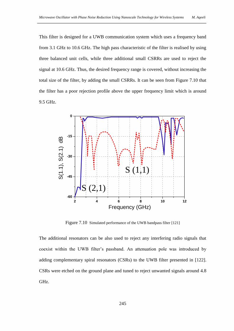
Microwave Oscillator with Phase Noise Reduction Using Nanoscale Technology for Wireless Systems M. Aqeeli
245
This filter is designed for a UWB communication system which uses a frequency band
from 3.1 GHz to 10.6 GHz. The high pass characteristic of the filter is realised by using
three balanced unit cells, while three additional small CSRRs are used to reject the
signal at 10.6 GHz. Thus, the desired frequency range is covered, without increasing the
total size of the filter, by adding the small CSRRs. It can be seen from Figure 7.10 that
the filter has a poor rejection profile above the upper frequency limit which is around
9.5 GHz.
2 4 6 8 10 12
-60
-45
-30
-15
0
S(1
.1),
S(2
.1)
dB
Frequency (GHz)
S (1,1)
S (2,1)
Figure 7.10 Simulated performance of the UWB bandpass filter [121]
The additional resonators can be also used to reject any interfering radio signals that
coexist within the UWB filter’s passband. An attenuation pole was introduced by
adding complementary spiral resonators (CSRs) to the UWB filter presented in [122].
CSRs were etched on the ground plane and tuned to reject unwanted signals around 4.8
GHz.

Microwave Oscillator with Phase Noise Reduction Using Nanoscale Technology for Wireless Systems M. Aqeeli
246
An open split ring resonator (OSRR), shown in Figure 7.11, is another attractive
component in the design of compact microstrip bandpass filters. The resonance
frequency of the filter is controlled by the geometric parameters of the OSRR, whereas
its bandwidth is adjusted according to the length of the transmission lines connected to
the OSRR.
OSRR
Top view
Bottom view
Figure 7.11 Top and bottom views of the open split ring resonator connected to a microstrip line [123]
OSRR-based filters are smaller in electrical size when compared to SRR- or CSRR-
based filters. Cascading multiple OSRRs in series with a microstrip line is the first
approach taken when designing OSRR-based filters. The second approach involves
connecting the OSRR with quarter-wave microstrip lines with various characteristic

Microwave Oscillator with Phase Noise Reduction Using Nanoscale Technology for Wireless Systems M. Aqeeli
247
impedances [124]. The desired filter response using this approach is achieved by
carefully calculating the impedance of the quarter-wave microstrip lines. Both of these
design approaches suffer from spurious passbands above the desired transmission
bands, which degrades filter performance.
To overcome OSRR design limitations, a double-sided open split ring resonator
DOSRR, shown in Figure 7.12, is introduced in [125], to increase the selectivity of the
filter by introducing an additional transmission zero. DOSRR combines two OSRRs
aligned in an inverted fashion over the top and bottom layers of the substrate. By using
the same physical size of the OSRR, DOSRR has the ability to introduce a transmission
zero located above the transmission pole of the filter. Two design strategies are
suggested in [125] to supress spurious passbands. The first strategy is to use the exact
circular shape of the DOSRR cell placed on both the top and the bottom layer of the
substrate. Etching a circular window instead of a square one on the bottom layer of the
DOSRR enables us to shift the spurious passbands upwards. Another approach is to
introduce U-shaped slots into the microstrip line, which will lead to an additional extra
transmission zero to achieve a wider upper stopband.
CRLH TL based on LC-loaded TL is another approach that can be used in filter design.
C. Tseng et al. presented dual-band bandpass and bandstop filters based on CRLH TL.
The main advantage of using CRLH TL over quarter-wave open-circuited and short-
circuited options in a conventional filter is that the passband/stopband of the filter can
be chosen, and it is not limited to the odd harmonics of the designed centre frequency f0.

Microwave Oscillator with Phase Noise Reduction Using Nanoscale Technology for Wireless Systems M. Aqeeli
248
OSRR
Top view
gc
dc
r
εr
g
D
Bottom view
Ground plane window
Figure 7.12 Top and bottom views of the DOSRR [123]
One of the most promising LH MTM structures is presented in [104]. In this structure, a
microstrip TL is loaded with CSRR and capacitive coupling on the top layer, in order to
produce negative permittivity and negative permeability simultaneously. It was shown
earlier that LH MTM structures can be realised through complex designs which either
require using through holes, known as via, for a quasi-lumped approach, or using a
defected ground structure (DGS) for the resonant-type LH TL. These requirements can
increase losses and introduce parasitic couplings between vias. Thus, it can be seen that

Microwave Oscillator with Phase Noise Reduction Using Nanoscale Technology for Wireless Systems M. Aqeeli
249
the design of the LH TL proposed by the authors in the present study is simple and
easier to fabricate, and undesirable effects from using the via and DGS can be avoided.
7.6: Feedback oscillator
A feedback oscillator is the most common type of harmonic oscillator, and its basic
operation can be explained with the linear feedback circuit shown in Figure 7.13. An
amplifier with voltage gain A is operated in a feedback loop where its output is fed back
into its input through a feedback network with a resonator or a bandpass filter.
O/P
Network
Amplifier
Resonator
BPF
R L
Figure 7.13 Feedback oscillator.
The resonant circuit Q is a significant design parameter that affects oscillator
performance, as mentioned in Leeson’s oscillator model [20]. The output oscillation
spectrum Sϕ(δω) can be written as:
0( ) 1
2S S
Q
(7.3)
where 𝛿𝜔 is the offset frequency from the oscillation frequency 𝜔0, 𝑆∆𝜃 is the additive
noise element and the quality factor of the oscillator, Q, represents any loss in the

Microwave Oscillator with Phase Noise Reduction Using Nanoscale Technology for Wireless Systems M. Aqeeli
250
resonant circuit. The conventional Q factor definition can be generally be defined
as[126]:
average energy stored.
energy loss/secondQ (7.4)
Q can be also defined with respect to the phase response of the resonator. It will be
denoted here as Qr to distinguish it from the complex quality factor which will be
defined later. High Qr resonators are used to increase the Q of the oscillator [127]. The
quality factor of the resonator can be defined as[128]:
0
0 0( )
2 2r d
dQ
d
(7.5)
where 𝜔0 is the oscillation frequency, ∅(𝜔0) is the phase response of the resonator and
𝜏𝑑 is the group delay. A bandpass filter can be used as a feedback network in the
oscillator design, as shown in Figure 7.13.
The impedance matrix Z can be used to represent the frequency response of the
bandpass filter. In [129], a complex quality factor, Qsc, is introduced which takes into
account the derivative of both the amplitude and the phase response of the filter with
respect to the frequency. It can be defined as:
0 011 11
12 12
ln2 2
sc
z zd dQ j
d z d z
(7.6)
Qsc is more rigorous than Qr, since it takes into account the effects of the amplitude and
the phase response of the filter. In the next section, a feedback oscillator will be
designed, using a left-handed bandpass filter. Furthermore, it will be designed at the
Microwave Oscillator with Phase Noise Reduction Using Nanoscale Technology for Wireless Systems M. Aqeeli
251
group delay peak and complex quality factor peak frequencies, to compare phase noise
results.
7.7: Oscillator design using an LH bandpass filter
An oscillator is considered an essential part of any wireless communication system.
Many design methods have been reported [130], [131] to meet oscillator design
requirements, namely low phase noise, low cost in comparison to the CMOS LC-
oscillator and low power consumption. The first design approach involves using high Q
resonators, such as a dielectric resonator, to design low phase noise oscillators [130].
On the other hand, the integration of the dielectric resonator with other planar circuits is
difficult, and it cannot be designed and implemented in the integrated circuit (IC)
process.
A planar microwave oscillator is proposed in [132-134] to mitigate the problems
observed in the high Q resonator-based oscillator. A four-pole elliptic-response filter is
used as a frequency-selective parameter to design a feedback oscillator [132]. Since
transmission zeros are present in their transfer function, elliptic filters have considerable
group-delay peaks at the corner frequencies of the passband, which makes them capable
of achieving considerable loaded quality factors.
Leeson derived an approximate equation specified for phase noise in a feedback
oscillator [135], which defines the single-sideband noise power (PSB) relative to the
oscillator output power (PC) as
1
. 1.
SB c
C C m d m
P LFKT
P P
(7.7)

Microwave Oscillator with Phase Noise Reduction Using Nanoscale Technology for Wireless Systems M. Aqeeli
252
where F is the amplifier excess noise figure, L is the insertion loss for the frequency
selective element used in the feedback, T is ambient temperature, K is the Boltzmann
constant, ωc is the flicker noise corner frequency, ωm is the offset frequency and τd is the
group delay of the feedback path. Equation 7.7 shows that phase noise is reduced as the
group delay increased. Consequently, designing the oscillation frequency at the group
delay peak frequency will improve phase noise performance. The authors in [136]
extended the passive four-pole filter mentioned in [41], to turn it into an active filter and
to further reduce the phase noise of the oscillator. Better performance is achieved at the
expense of increasing manufacturing cost, since two microwave transistors are needed.
Another major drawback of using conventional filters, such as elliptic, in feedback
oscillator design is that it requires a larger circuit size when compared to metamaterial
filters. Figure 7.14 shows the layout of a bandpass filter with a four-pole elliptic
implemented in [50], which has an electrical size of 0.49λg × 0.5λg. In [132], the authors
explained that the Qr peak frequency value might not match the oscillator’s Q value.
Therefore, the best phase noise performance might not be obtained, and so they
suggested using frequencies at the Qsc peak.
In the next section, a novel narrowband BPF is presented which consists of two CRLH
transmission line unit cells. Group-delay peak and complex quality factor Qsc peak are
both evaluated and used to design the proposed oscillator with low phase noise. The
results show that a significant reduction in phase noise can be obtained at the Qsc peak
frequency.

Microwave Oscillator with Phase Noise Reduction Using Nanoscale Technology for Wireless Systems M. Aqeeli
253
12.6 mm
12
.4 m
m
Figure 7.14 Layout of a four-pole elliptic filter [132]
7.8: Filter design using LH transmission line unit
cells
An LH structure can be constructed using different design approaches. The hybrid
approach combines resonators with shunt grounded inductances and series capacitive
gaps [137]. The advantage of this approach is that transmission zero exists right on the
top of the left-handed region, which makes it suitable for designing compact filters with
good out-of-band rejection levels. Moreover, ground plane etching is avoided by
presenting CSRR, series gaps and shunt inductive stubs onto the top metallic layer, as
shown in Figure 7.15 (a). The CSRRs are the most important part of the unit cell and are
represented in the circuit by Lc and Cc and coupled to the line by C, as shown in Figure
7.15 (b). The coupling of the CSRRs to the line will be controlled by its total area.
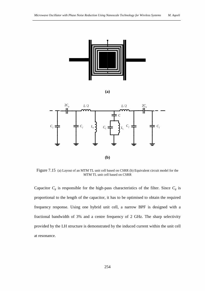
Microwave Oscillator with Phase Noise Reduction Using Nanoscale Technology for Wireless Systems M. Aqeeli
254
(a)
2 gC 2 gC/ 2L
fCfCfC fC
cLCCdL
/ 2L
C
(b)
Figure 7.15 (a) Layout of an MTM TL unit cell based on CSRR (b) Equivalent circuit model for the
MTM TL unit cell based on CSRR
Capacitor Cg is responsible for the high-pass characteristics of the filter. Since Cg is
proportional to the length of the capacitor, it has to be optimised to obtain the required
frequency response. Using one hybrid unit cell, a narrow BPF is designed with a
fractional bandwidth of 3% and a centre frequency of 2 GHz. The sharp selectivity
provided by the LH structure is demonstrated by the induced current within the unit cell
at resonance.

Microwave Oscillator with Phase Noise Reduction Using Nanoscale Technology for Wireless Systems M. Aqeeli
255
The induced current is confined by the effective capacitance between the gaps. The
inductance and capacitance of the unit cell can be optimised by varying the number of
concentric rings and gaps between them. The simulated s-parameter results for the filter
are presented in Figure 7.16.
1.0 1.5 2.0 2.5 3.0
-39.6
-35.2
-30.8
-26.4
-22.0
-17.6
-13.2
-8.8
-4.4
0.0
Magnitude (
dB
)
Frequency (GHz)
S21
S11
Figure 7.16 Simulated s-parameter results for the hybrid unit cell
The existence of negative permittivity and negative permeability regions in the
passband can be verified by using the S-parameter retrieval method outlined in [140].
It can be seen in Figure 7.17 that the proposed filter shows that the BPF exhibits a left-
handed passband from 2 to 2.05 GHz and right-handed passband from 1.96 to 2 GHz.
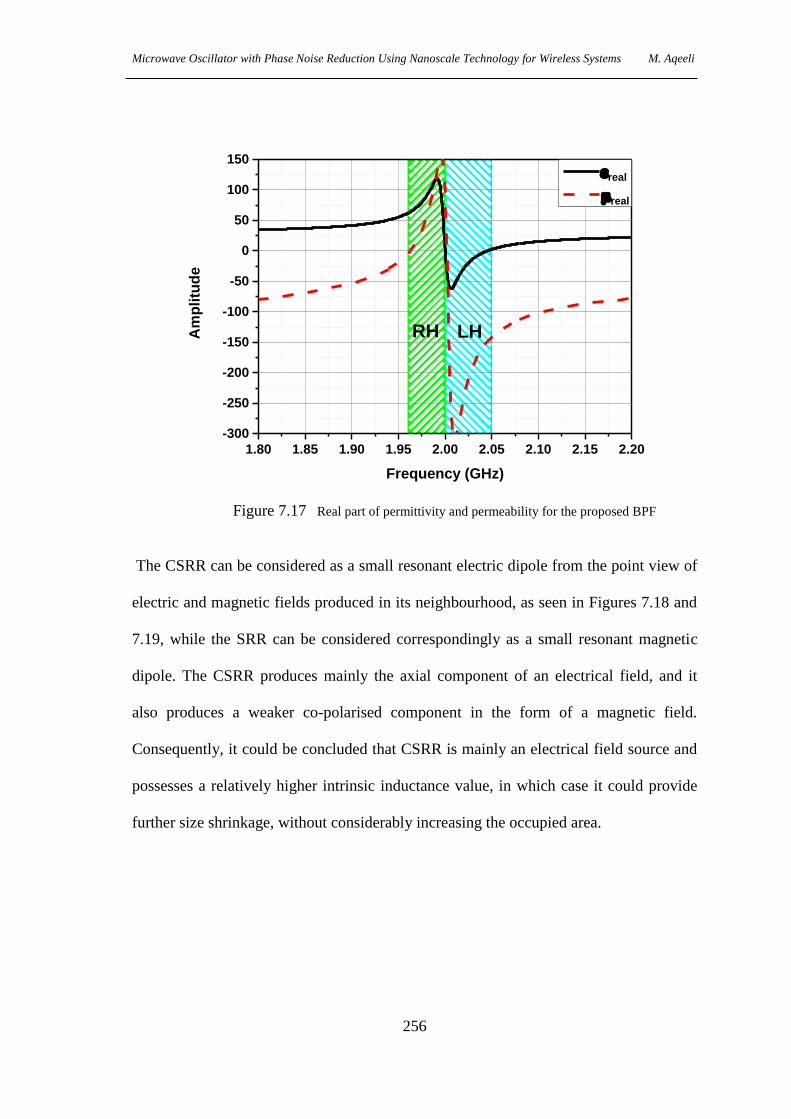
Microwave Oscillator with Phase Noise Reduction Using Nanoscale Technology for Wireless Systems M. Aqeeli
256
1.80 1.85 1.90 1.95 2.00 2.05 2.10 2.15 2.20
-300
-250
-200
-150
-100
-50
0
50
100
150
Am
plitu
de
Frequency (GHz)
real
real
RH LH
Figure 7.17 Real part of permittivity and permeability for the proposed BPF
The CSRR can be considered as a small resonant electric dipole from the point view of
electric and magnetic fields produced in its neighbourhood, as seen in Figures 7.18 and
7.19, while the SRR can be considered correspondingly as a small resonant magnetic
dipole. The CSRR produces mainly the axial component of an electrical field, and it
also produces a weaker co-polarised component in the form of a magnetic field.
Consequently, it could be concluded that CSRR is mainly an electrical field source and
possesses a relatively higher intrinsic inductance value, in which case it could provide
further size shrinkage, without considerably increasing the occupied area.

Microwave Oscillator with Phase Noise Reduction Using Nanoscale Technology for Wireless Systems M. Aqeeli
257
Figure 7.18 Simulated electrical field at the resonance frequency for one unit cell
Figure 7.19 Simulated magnetic field at the resonance frequency for one unit cell
Due to the presence of transmission zero in the lower stopband, a large group delay is
generated at the passband’s edge, thereby increasing the capability of the CSRR-based
filter to provide a high quality factor. The transmission zero located at 1.75 GHz is due
to the grounded series resonator, as seen in the equivalent circuit model in Figure

Microwave Oscillator with Phase Noise Reduction Using Nanoscale Technology for Wireless Systems M. Aqeeli
258
7.15(b). The simulated group delay results show that the filter has a group delay peak =
3.8 ns at 1.99 GHz, as shown in Figure 7.20.
1.8 1.9 2.0 2.1 2.20
1
2
3
4
G
rou
p D
ea
ly (
ns)
Frequency (GHz)
Group Dealy
Figure 7.20 Simulated group delay results for the hybrid unit cell
Using two unit cells, where the capacitive coupling between them is relatively weak,
allows for the increment in the group delay peak value. It is a valid assumption for any
multi-resonator structure that there will be trade-offs between the group delay,
bandwidth and insertion loss. Decreasing the coupling between resonators allows for the
increment of the group delay value at the expense of the other factors. Since bandwidth
is not a critical parameter for the oscillator design application, insertion loss becomes
the only limiting factor for the minimum allowable value of coupling between
resonators. The designed structure using two unit cells might look complicated to some
extent. In order to illustrate the design consideration of the unit cell, the unit cell used in
the proposed filter is compared to a simple CRLH TL unit cell shown in Figure 7.21.

Microwave Oscillator with Phase Noise Reduction Using Nanoscale Technology for Wireless Systems M. Aqeeli
259
Figure 7.21 Simple CSRR based Filter
The simulated S21 results show that insertion loss was slightly improved, as shown in
Figure 7.22, whereas the selectivity of the filter degraded significantly when using the
simple structure.
1.0 1.5 2.0 2.5 3.0
-70
-60
-50
-40
-30
-20
-10
0
S2
1 (
dB
)
Frequency (GHz)
Proposed Filter
Simple CSRR Filter
S21=-2.65 dB S21=-3 dB
Figure 7.22 Simulated results of S21 for the proposed filter and simple structure
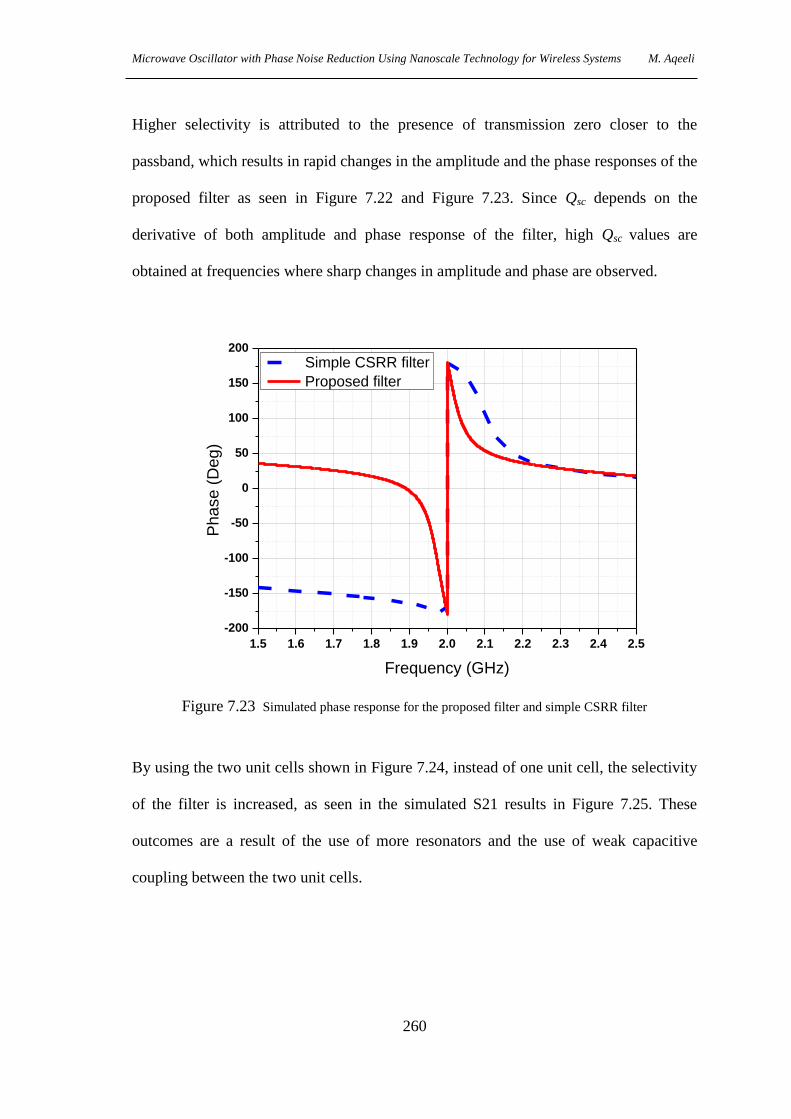
Microwave Oscillator with Phase Noise Reduction Using Nanoscale Technology for Wireless Systems M. Aqeeli
260
Higher selectivity is attributed to the presence of transmission zero closer to the
passband, which results in rapid changes in the amplitude and the phase responses of the
proposed filter as seen in Figure 7.22 and Figure 7.23. Since Qsc depends on the
derivative of both amplitude and phase response of the filter, high Qsc values are
obtained at frequencies where sharp changes in amplitude and phase are observed.
1.5 1.6 1.7 1.8 1.9 2.0 2.1 2.2 2.3 2.4 2.5
-200
-150
-100
-50
0
50
100
150
200
Phase (
Deg
)
Frequency (GHz)
Simple CSRR filter
Proposed filter
Figure 7.23 Simulated phase response for the proposed filter and simple CSRR filter
By using the two unit cells shown in Figure 7.24, instead of one unit cell, the selectivity
of the filter is increased, as seen in the simulated S21 results in Figure 7.25. These
outcomes are a result of the use of more resonators and the use of weak capacitive
coupling between the two unit cells.

Microwave Oscillator with Phase Noise Reduction Using Nanoscale Technology for Wireless Systems M. Aqeeli
261
5.00mm
1.95mm
0.12mm
1.70mm
4.92mm
1.10mm
5.8
3m
m
0.30mm
0.30mm4.9
5m
m
5.8
3m
m
9.40mm
1.57mm
Figure 7.24 Layout of the proposed LH BPF
1.0 1.5 2.0 2.5 3.0
-50
-40
-30
-20
-10
0
S21 (
dB
)
Frequency (GHz)
2 cells
1 cell
Figure 7.25 Simulated S21 results for a narrowband BPF based on one and two unit cells
Moreover, the higher selectivity of the filter leads to a higher Q, which can be easily
translated into a larger group delay peak, as explained in equation 7.5 and proven by the
simulation results in Figure 7.26.

Microwave Oscillator with Phase Noise Reduction Using Nanoscale Technology for Wireless Systems M. Aqeeli
262
1.8 1.9 2.0 2.1 2.20
1
2
3
4
5
6
7
Gro
up D
ela
y (n
s)
Frequency (GHz)
Group Delay
Figure 7.26 Simulated group delay results for the BPF using two hybrid unit cells
Using equation (7.6), magnitude of Qsc is plotted for the proposed BPF in Figure 7.27,
where two Qsc peaks are observed at 1.975 GHz and 2.05 GHz.
1.80 1.85 1.90 1.95 2.00 2.05 2.10 2.15 2.20
0
20
40
60
80
100
120
140
160
180
200
Co
mp
lex Q
Frequency (GHz)
Qs=184
@1.975GHz
Qs=188
@2.050GHz
Figure 7.27 Complex quality factor for the BPF using two hybrid unit cells
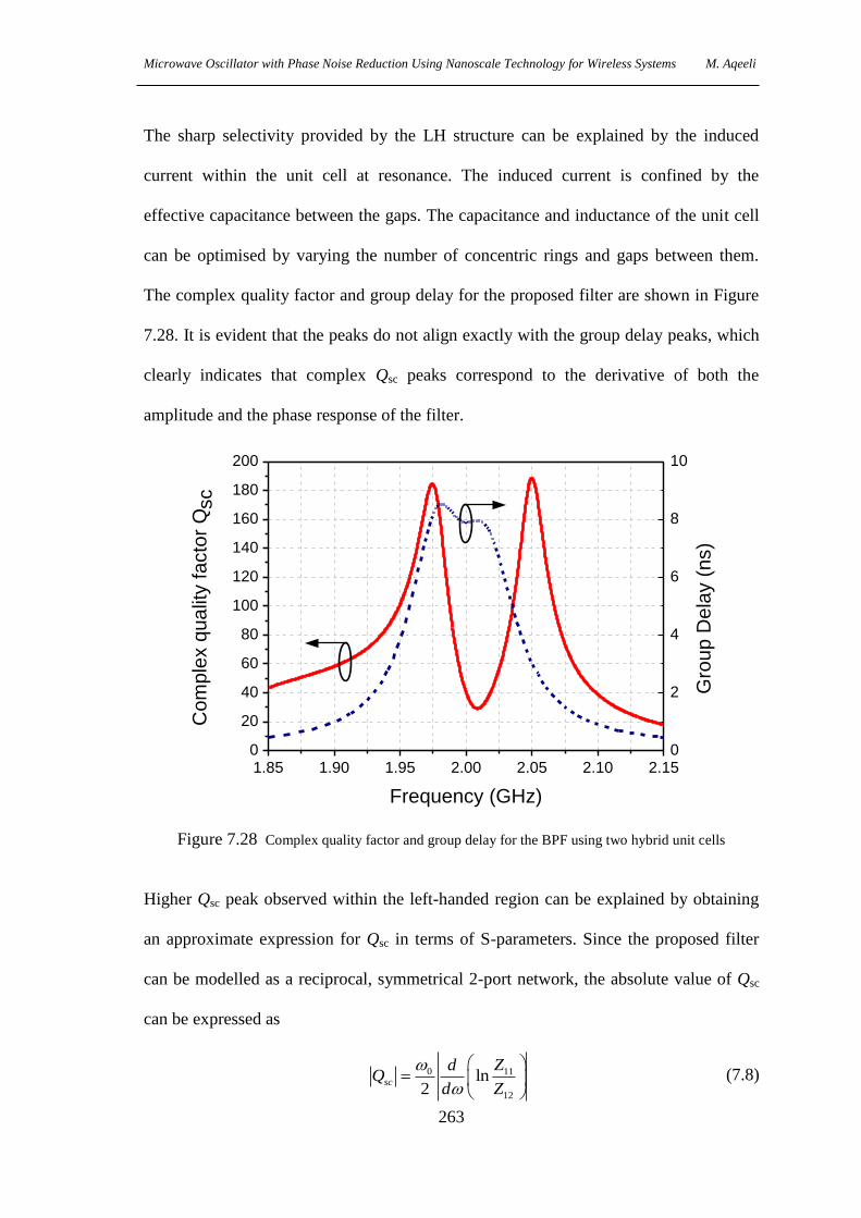
Microwave Oscillator with Phase Noise Reduction Using Nanoscale Technology for Wireless Systems M. Aqeeli
263
The sharp selectivity provided by the LH structure can be explained by the induced
current within the unit cell at resonance. The induced current is confined by the
effective capacitance between the gaps. The capacitance and inductance of the unit cell
can be optimised by varying the number of concentric rings and gaps between them.
The complex quality factor and group delay for the proposed filter are shown in Figure
7.28. It is evident that the peaks do not align exactly with the group delay peaks, which
clearly indicates that complex Qsc peaks correspond to the derivative of both the
amplitude and the phase response of the filter.
1.85 1.90 1.95 2.00 2.05 2.10 2.150
20
40
60
80
100
120
140
160
180
200
Co
mp
lex q
ua
lity f
acto
r Q
sc
Frequency (GHz)
0
2
4
6
8
10
Gro
up
De
lay (
ns)
Figure 7.28 Complex quality factor and group delay for the BPF using two hybrid unit cells
Higher Qsc peak observed within the left-handed region can be explained by obtaining
an approximate expression for Qsc in terms of S-parameters. Since the proposed filter
can be modelled as a reciprocal, symmetrical 2-port network, the absolute value of Qsc
can be expressed as
0 11
12
ln2
sc
ZdQ
d Z
(7.8)
Microwave Oscillator with Phase Noise Reduction Using Nanoscale Technology for Wireless Systems M. Aqeeli
264
And the impedance parameters of the 2-port network are defined as
11 22 12 21 0
11
11 22 12 21
(1 )(1 )
(1 )(1 )
S S S S ZZ
S S S S
(7.9)
12 012
11 22 12 21
2
(1 )(1 )
S ZZ
S S S S
(7.10)
Where S21 and S11 are the insertion loss and return loss of the filter. Assuming S11=S22
and S12=S21 for reciprocal 2-port network, the following relation is obtained:
2 2
11 11 21
21 21
1
2
Z S S
Z S
(7.11)
Equation 7.11 can be applied to a 2-port network realised by the proposed bandpass
filter and S11 and S21 can be expanded at ω=ω0 as
11 11 0 11 0( ) ( ) ( )d
S S Sd
(7.12)
21 21 0 21 0( ) ( ) ( )d
S S Sd
(7.13)
Where ω0 is the centre frequency of the bandpass filter and by assuming the following
for the filter:
11 0( ) 1S , 11 0( ) 1d
Sd
, 21 0( )S Insertion loss=IL, 21 0( ) 1
dS
d

Microwave Oscillator with Phase Noise Reduction Using Nanoscale Technology for Wireless Systems M. Aqeeli
265
21 0arg( )d
S atd
=-group delay=-τg, According to (7.8) and (7.11), Qsc is calculated in
terms of S-parameters as
2 2
0 11 21
21
1ln
2 2sc
S SdQ
d S
(7.14)
Taking the derivative of (7.14), the following formula for Qsc is obtained:
0
2sc gQ
at 0 (7.15)
Since group velocity, vg, is the inverse of the group delay per unit length, LT, Qsc can be
written as
0
2
Tsc
g
LQ
v
at 0 (7.16)
Electromagnetic propagation within LH region is characterized by low group velocity
(134), hence higher Qsc is obtained within the LH region.
7.9: Oscillator design at Qsc and the group delay peak
frequency
Two elements are required to design a filter-based oscillator: an amplifier and a
bandpass filter. The BFP405 bipolar transistor, manufactured by Infineon is biased at
Vcc= 2.135 V with a collector current Ic= 2.85 mA. It was used to realise the amplifier
shown in Figure 7.29. The author used the same amplifier in [38] to observe the effect
of filters based on an LH transmission line unit cell.
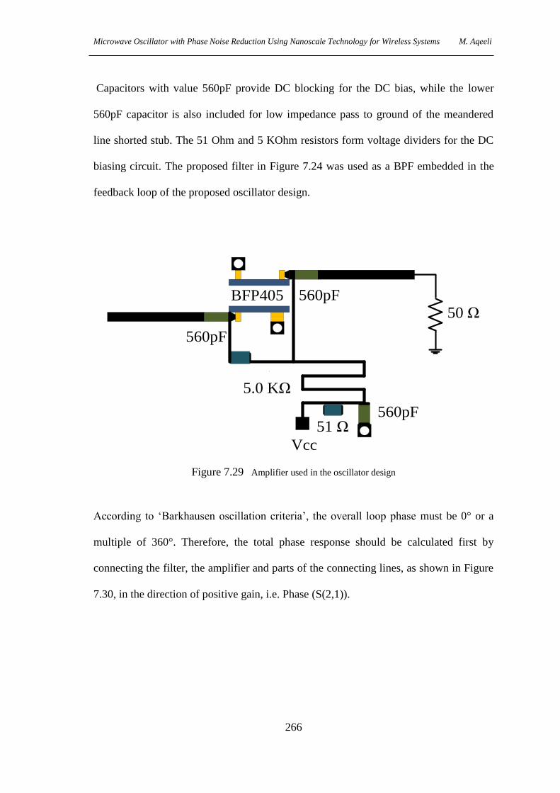
Microwave Oscillator with Phase Noise Reduction Using Nanoscale Technology for Wireless Systems M. Aqeeli
266
Capacitors with value 560pF provide DC blocking for the DC bias, while the lower
560pF capacitor is also included for low impedance pass to ground of the meandered
line shorted stub. The 51 Ohm and 5 KOhm resistors form voltage dividers for the DC
biasing circuit. The proposed filter in Figure 7.24 was used as a BPF embedded in the
feedback loop of the proposed oscillator design.
BFP40550 Ω
51 Ω
560pF
Vcc
560pF
560pF
5.0 KΩ
Figure 7.29 Amplifier used in the oscillator design
According to ‘Barkhausen oscillation criteria’, the overall loop phase must be 0° or a
multiple of 360°. Therefore, the total phase response should be calculated first by
connecting the filter, the amplifier and parts of the connecting lines, as shown in Figure
7.30, in the direction of positive gain, i.e. Phase (S(2,1)).

Microwave Oscillator with Phase Noise Reduction Using Nanoscale Technology for Wireless Systems M. Aqeeli
267
Figure 7.30 Schematics of the filter with the amplifier, parts of connecting lines
The length of the transmission line needed to connect port 1 to port 2 is determined
using the phase values at Qsc and group delay peak frequencies indicated in Figure 7.31.
1.80 1.85 1.90 1.95 2.00 2.05 2.10 2.15 2.20
-300
-250
-200
-150
-100
-50
0
50
100
Ph
ase
(d
eg
)
Frequency (GHz)
Phase =-69.592 deg
@ 1.970 GHzPhase =-236.110 deg
@ 2.050 GHz
Figure 7.31 Phase response of the amplifier with the filter and parts of connecting lines

Microwave Oscillator with Phase Noise Reduction Using Nanoscale Technology for Wireless Systems M. Aqeeli
268
The width of the connecting microstrip transmission line is easily calculated by
considering the analytical line impedance at the centre frequency of the LH BPF. Using
Taconic RF-35 substrate, with a thickness of 0.508 mm and a loss tangent of 0.0018 and
dielectric constant of 3.5, the width of the connecting lines is chosen to be 1.1 mm to
reach 50 ohm characteristic impedance.The schematic of the designed oscillator at Qsc
peak frequency is shown in Figure 7.33. The circuit analysis has been performed with
ADS oscport module within Harmonic balance (HB) solver, as depicted in Figure 7.32.
Figure 7.32 Schematics diagram of the proposed filter based oscillator

Microwave Oscillator with Phase Noise Reduction Using Nanoscale Technology for Wireless Systems M. Aqeeli
269
Figure 7.33 Schematic of the oscillator designed at Qsc peak frequency
The simulated output power for the oscillator designed at Qsc peak is 4.8 dBm at the
oscillation frequency of 2.05 GHz, as shown in Figure 7.34. The DC power consumed
by the oscillator is 6.1 mW. The simulated phase noises are -126 dBc/Hz at 100 kHz
and -152.1 dBc/Hz at 1 MHz offset frequencies, as presented in Figure 7.35. The FoM
of the designed oscillator at a 1-MHz offset frequency is -207 dBc/Hz. The significant
reduction of the phase noise observed in the simulation results of the proposed oscillator
confirms that LH BPF is capable of providing high Qsc peak which is mainly attributed
to the slow-wave propagation property of LH structure.
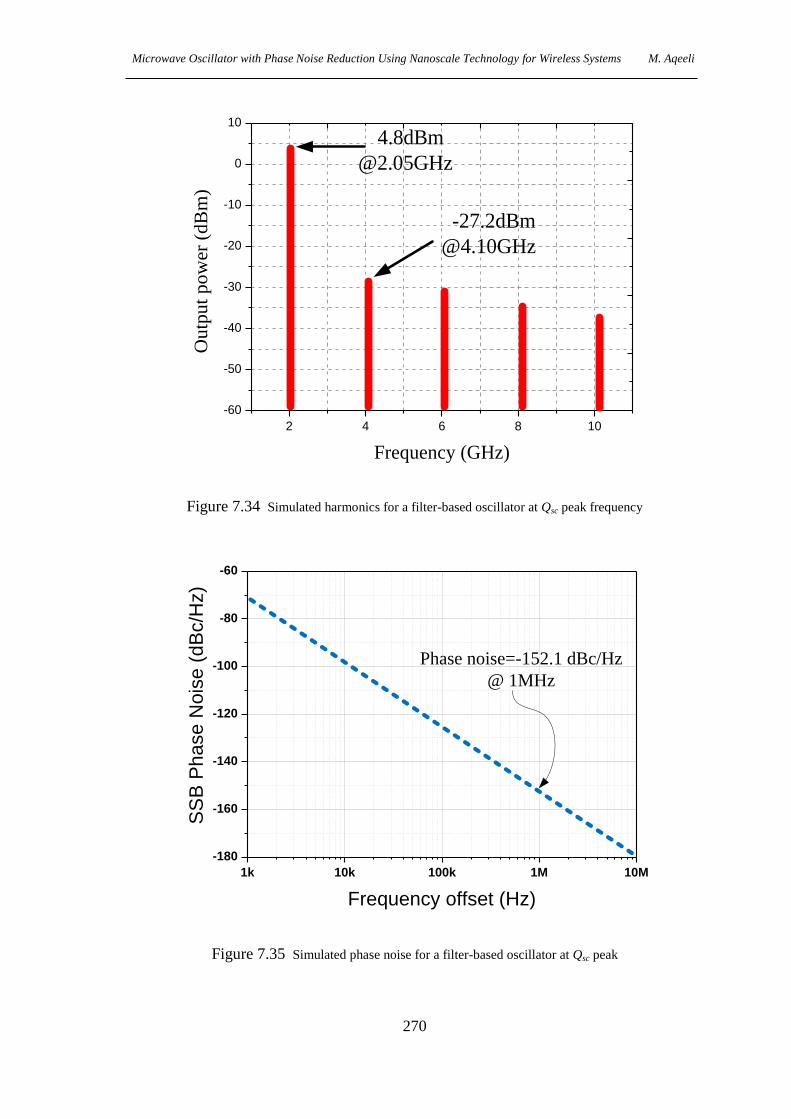
Microwave Oscillator with Phase Noise Reduction Using Nanoscale Technology for Wireless Systems M. Aqeeli
270
2 4 6 8 10
-60
-50
-40
-30
-20
-10
0
10
Ou
tpu
t p
ow
er (
dB
m)
Frequency (GHz)
4.8dBm
@2.05GHz
-27.2dBm
@4.10GHz
Figure 7.34 Simulated harmonics for a filter-based oscillator at Qsc peak frequency
1k 10k 100k 1M 10M
-180
-160
-140
-120
-100
-80
-60
SS
B P
ha
se
No
ise
(d
Bc/H
z)
Frequency offset (Hz)
Phase noise=-152.1 dBc/Hz
@ 1MHz
Figure 7.35 Simulated phase noise for a filter-based oscillator at Qsc peak

Microwave Oscillator with Phase Noise Reduction Using Nanoscale Technology for Wireless Systems M. Aqeeli
271
By changing the length of the connecting transmission line between port 1 and port 2,
the oscillator can be designed to oscillate at the group delay peak frequency of 1.971
GHz, as shown in Figure 7.36. It can be seen that the length of the connecting line is
reduced to 63.9 mm to satisfy Barkhausen oscillation criteria at the group delay peak
frequency.
Figure 7.36 Schematic of the proposed oscillator, designed and implemented at group delay peak
frequency
The simulated output power for the proposed oscillator is 2.168 dBm, as shown in
Figure 7.37 where the oscillation frequency is designed at group delay peak. The
simulated phase noises are -116.1 dBc/Hz and -142.5 dBc/Hz at 100-kHz and 1-MHz
offset frequencies, as presented in Figure 7.38.

Microwave Oscillator with Phase Noise Reduction Using Nanoscale Technology for Wireless Systems M. Aqeeli
272
2 4 6 8 10
-60
-50
-40
-30
-20
-10
0
10
Outp
ut po
wer
(dB
m)
Frequency (GHz)
2.6dBm
@2.05GHz -17.3dBm
@4.10GHz
Figure 7.37 Simulated output spectrum and phase noise for the oscillator designed at group delay peak
frequency
1k 10k 100k 1M 10M
-165
-150
-135
-120
-105
-90
-75
-60
SS
B P
hase N
ois
e (
dB
c/H
z)
Frequency offset (Hz)
Phase noise=-142.5 dBc/Hz
@ 1MHz
Figure 7.38 Simulated phase noise for the filter-based oscillator at group delay peak frequency
The simulation results show that significant phase noise reduction is attained when

Microwave Oscillator with Phase Noise Reduction Using Nanoscale Technology for Wireless Systems M. Aqeeli
273
designing the oscillator at the Qsc peak instead of the group delay peak. Figure 7.39
shows the layout of the proposed oscillator, which is designed using an LH
metamaterial BPF and is fabricated on a Taconic RF-35 substrate, with a thickness of
0.508 mm, a loss tangent of 0.0018 and a dielectric constant of 3.5. The fabricated
oscillator is shown in Figure 7.40.
BFP40550 Ω
5.0mm
5.0mm
51 Ω
560pF
560pF
560pF
Input
Output
5.0 KΩ
Vcc
Figure 7.39 Layout of the proposed feedback oscillator
Figure 7.40 Circuit photograph of the oscillator designed at Qsc peak frequency
Agilent E5052B source signal analyzer is a piece of measurement equipment that can
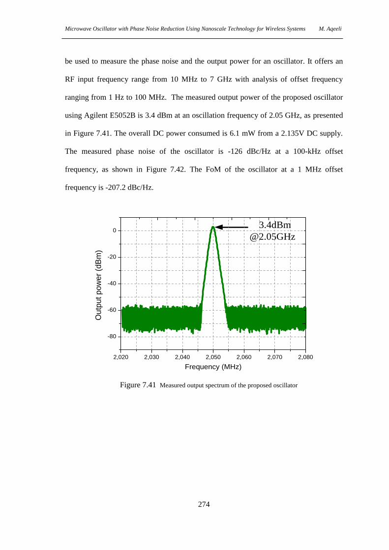
Microwave Oscillator with Phase Noise Reduction Using Nanoscale Technology for Wireless Systems M. Aqeeli
274
be used to measure the phase noise and the output power for an oscillator. It offers an
RF input frequency range from 10 MHz to 7 GHz with analysis of offset frequency
ranging from 1 Hz to 100 MHz. The measured output power of the proposed oscillator
using Agilent E5052B is 3.4 dBm at an oscillation frequency of 2.05 GHz, as presented
in Figure 7.41. The overall DC power consumed is 6.1 mW from a 2.135V DC supply.
The measured phase noise of the oscillator is -126 dBc/Hz at a 100-kHz offset
frequency, as shown in Figure 7.42. The FoM of the oscillator at a 1 MHz offset
frequency is -207.2 dBc/Hz.
3.4dBm
@2.05GHz
2,020 2,030 2,040 2,050 2,060 2,070 2,080
-80
-60
-40
-20
0
Ou
tpu
t p
ow
er
(dB
m)
Frequency (MHz)
Figure 7.41 Measured output spectrum of the proposed oscillator
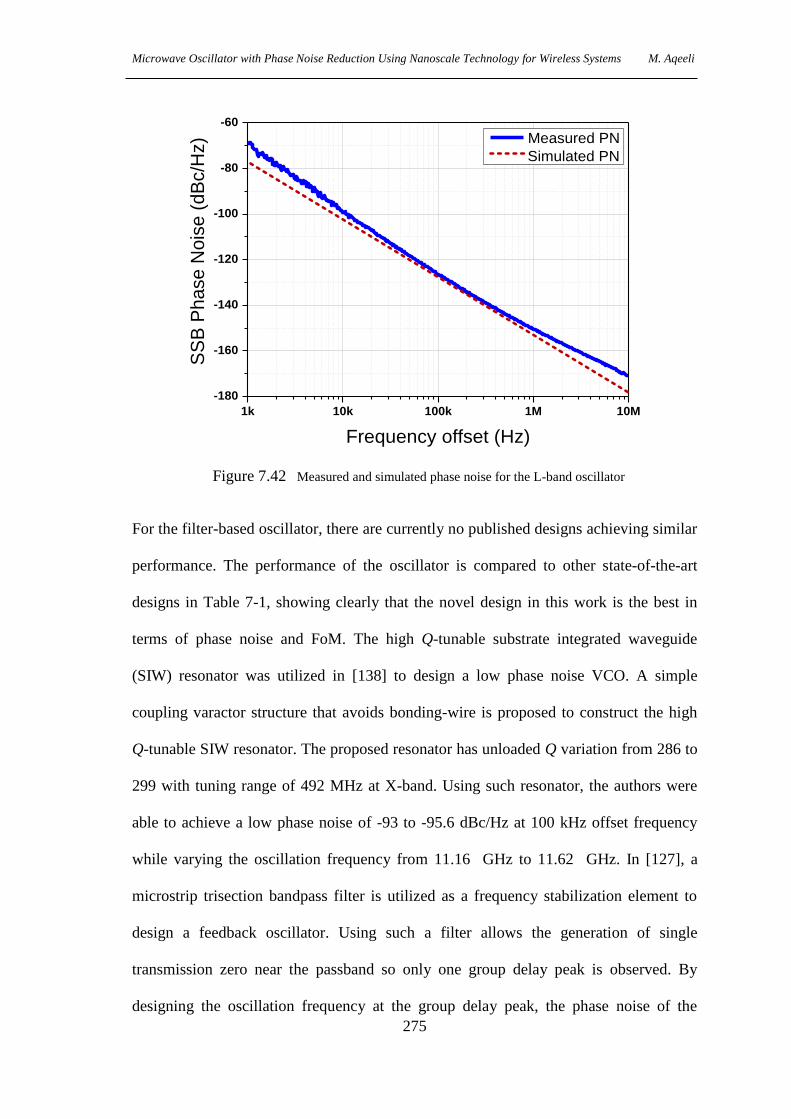
Microwave Oscillator with Phase Noise Reduction Using Nanoscale Technology for Wireless Systems M. Aqeeli
275
1k 10k 100k 1M 10M
-180
-160
-140
-120
-100
-80
-60
SS
B P
ha
se
No
ise
(d
Bc/H
z)
Frequency offset (Hz)
Measured PN
Simulated PN
Figure 7.42 Measured and simulated phase noise for the L-band oscillator
For the filter-based oscillator, there are currently no published designs achieving similar
performance. The performance of the oscillator is compared to other state-of-the-art
designs in Table 7-1, showing clearly that the novel design in this work is the best in
terms of phase noise and FoM. The high Q-tunable substrate integrated waveguide
(SIW) resonator was utilized in [138] to design a low phase noise VCO. A simple
coupling varactor structure that avoids bonding-wire is proposed to construct the high
Q-tunable SIW resonator. The proposed resonator has unloaded Q variation from 286 to
299 with tuning range of 492 MHz at X-band. Using such resonator, the authors were
able to achieve a low phase noise of -93 to -95.6 dBc/Hz at 100 kHz offset frequency
while varying the oscillation frequency from 11.16 GHz to 11.62 GHz. In [127], a
microstrip trisection bandpass filter is utilized as a frequency stabilization element to
design a feedback oscillator. Using such a filter allows the generation of single
transmission zero near the passband so only one group delay peak is observed. By
designing the oscillation frequency at the group delay peak, the phase noise of the
Microwave Oscillator with Phase Noise Reduction Using Nanoscale Technology for Wireless Systems M. Aqeeli
276
oscillator is significantly reduced. The measured phase noise of the trisection bandpass
filter based oscillator is -120 dBc/Hz at an offset frequency of 100 kHz for an
oscillation frequency of 2.46 GHz. Complex quality factor Qsc was introduced in [129]
to take into account both amplitude and phase response of the bandpass filter used in
feedback oscillator design. Significant reduction in phase noise result was achieved by
designing the oscillation frequency at the Qsc peak instead of group delay peak. Since
the combline filter has a simple circuit structure, it was utilized to design a low phase
noise oscillator at the frequency of Qsc peak. The measured phase noise for the combline
filter based oscillator is -125.6 dBc/Hz at an offset frequency of 100 kHz from the
oscillation frequency of 2.04 GHz.
An SIW dual-mode BPF with circular cavity is first utilized to design an X-band low
phase noise oscillator in [134]. At microwave frequencies, higher quality factor values
are obtained using SIW cavity based BPF instead of conventional microstrip BPF.
Moreover, one large group delay peak is obtained near the upper passband to exclude
the design ambiguity introduced within elliptic-response BPF. Another parameter that
affects the phase noise performance in oscillator design is the insertion loss of the BPF.
Group delay can be maximized at the expense of increasing the insertion loss of the
filter. Therefore, the proposed SIW BPF was optimized to achieve the largest group
delay value while maintain an acceptable level of insertion loss.
Hairpin-shaped resonator (HSR) using composite right/left-handed transmission line
was proposed in [139]. CRLH TL and conventional TL are utilized to construct the
proposed resonator. High Q-factor obtained using such resonator is attributed to the
slow wave propagation property of the CRLH TL. High Q-factor and compact size are

Microwave Oscillator with Phase Noise Reduction Using Nanoscale Technology for Wireless Systems M. Aqeeli
277
two of the major requirements in microwave oscillator design to reduce the phase noise
and lower the cost of the manufacturing. Using the HSR, a microwave oscillator is
designed at an oscillation frequency of 4.95 GHz where a phase noise of -120.5 was
achieved at 100 kHz offset frequency with FOM of -206.3.
Table 7-1 Performance comparison between published oscillators and this study
Resonator/
Filter
F
(GHz)
PDC
(mW)
P0
(dBm)
PN
(dBc/Hz)
FoM
(dBc/Hz)
Ref.
SIW 11.4 20.00 2.60 -95.6 -193.1 [138]
Trisection 2.46 6.40 6.39 -120.4 -195.8 [127]
Combline 2.04 22.00 -0.68 -125.6 -201.1 [129]
Dual Mode SIW 11.6 11.40 -2.30 -117.3 -206.2 [134]
HSR 4.95 6.40 4.93 -120.5 -206.3 [139]
LH Metamaterial 2.05 6.10 3.40 -126.7 -207.2 This work F: Centre frequency, PDC: Power dissipated, P0: Output power, PN: Phase noise at 100 kHz, FoM measured at 1.0MHz
7.10: Chapter summary
In this chapter, a novel low phase noise free-running oscillator design based on high
selectivity metamaterial bandpass filter is presented. The bandpass filter is realized by
combining complementary split ring resonators with capacitive gaps and short
connected inductance to construct the composite right TL. The high selectivity of the
proposed filter is attributed to the use of the two unit cells instead of single unit cell and
the presence of transmission zero within the lower stopband.
The complex quality factor Qsc of proposed bandpass filter was studied and analyzed.
Qsc is a rigorous definition of the Q-factor which takes into accounts both amplitude and
phase response of the bandpass filter. It was observed that the proposed filter has higher

Microwave Oscillator with Phase Noise Reduction Using Nanoscale Technology for Wireless Systems M. Aqeeli
278
Qsc peak within the LH region when compared to the RH region. By deriving an
expression for Qsc in terms of S-parameters, it was concluded that Qsc is inversely
related to group velocity. Since electromagnetic propagation within LH region is
characterized by slow wave propagation, high Qsc peak value is attained within the LH
region. Based on the analysis of the complex quality factor Qsc for an LH narrowband
metamaterial filter, a novel, free-running oscillator has been designed to meet the most
stringent phase noise requirements in the L-band.
It can be concluded that the reported oscillator exhibits better performance and
significantly reduces phase noise compared to examples in published works to date. The
high performance specifications include measured phase noise of -126.7 dBc/Hz at an
offset frequency of 100 KHz away from 2.05 GHz, an FoM of -207.2 dBc/Hz, while the
oscillator core’s total power consumption is 6.1 mW from a 2.135V DC supply.
Microwave Oscillator with Phase Noise Reduction Using Nanoscale Technology for Wireless Systems M. Aqeeli
279
Electromagnetic Chapter 8:
Interference Shielding
based on Highly Flexible
and Conductive Graphene
Laminate
8.1: Introduction
A practical solution is to cover the electronic device with a shielding material to
restrains it from emitting radio frequency or electromagnetic energy. The shielding
material either absorbs or reflects the electromagnetic energy within the material.
Shielding effectiveness (SE) is defined as the ratio of the power received with and
without a material present
Microwave Oscillator with Phase Noise Reduction Using Nanoscale Technology for Wireless Systems M. Aqeeli
280
1
2
( ) 10logP
SE dBP
(8.1)
Where P1 is the received power with the material present, P2 is the received power
without the material present. A material that absorbs and/or reflects 99% of the
electromagnetic (EM) energy has a SE of 20 and may be used for shielding applications.
This research extends the potential of highly conductive graphene laminate to the
application of electromagnetic interference (EMI) shielding. In addition, it presents a
future proposal to study the effects of continuous wave electromagnetic interference
(EMI) on oscillators and VCOs.
8.2: The rise of graphene
Graphene is a new class of material which, due to its unique chemical, mechanical,
thermal, electronic and optical properties has attracted a lot of attention about its
potential applications in many fields. Graphene is a flat monolayer of carbon atoms
packed tightly into a two-dimensional honeycomb lattice as shown in Figure 8.1.
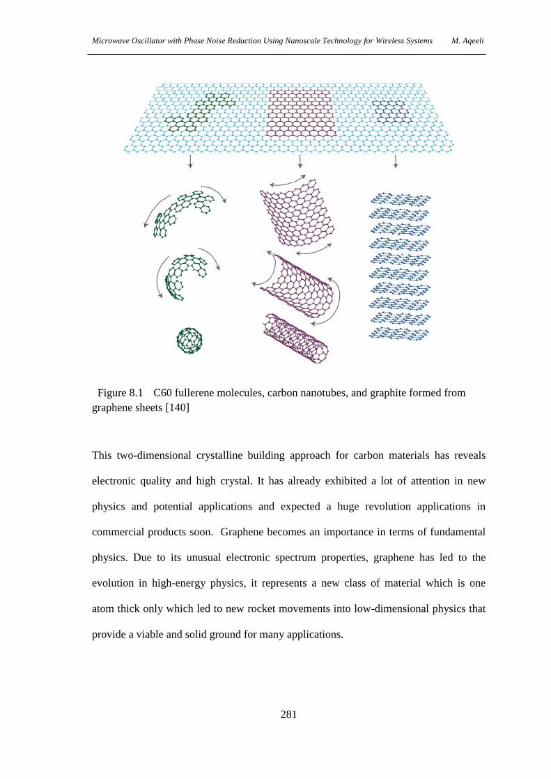
Microwave Oscillator with Phase Noise Reduction Using Nanoscale Technology for Wireless Systems M. Aqeeli
281
Figure 8.1 C60 fullerene molecules, carbon nanotubes, and graphite formed from
graphene sheets [140]
This two-dimensional crystalline building approach for carbon materials has reveals
electronic quality and high crystal. It has already exhibited a lot of attention in new
physics and potential applications and expected a huge revolution applications in
commercial products soon. Graphene becomes an importance in terms of fundamental
physics. Due to its unusual electronic spectrum properties, graphene has led to the
evolution in high-energy physics, it represents a new class of material which is one
atom thick only which led to new rocket movements into low-dimensional physics that
provide a viable and solid ground for many applications.

Microwave Oscillator with Phase Noise Reduction Using Nanoscale Technology for Wireless Systems M. Aqeeli
282
The Nobel Prize in Physics 2010 honoured two scientists, Sir Andre Geim and Sir
Konstantin S. Novoselov, both at the University of Manchester. This was for their
successfully producing, identifying isolating and characterizing graphene.
Graphene, is a planar atomic layer of carbon atoms bonded in a hexagonal structure. It
is an excellent material in emerging nanoelectronic applications [141]. Graphene’s band
structure, together with it’s high degree thinness, leads to a very noticeable electric field
and Hall effects [142-144]. Intrinsic graphene is a zero bandgap semiconductor, and its
conductivity can be tuned by either magnetostatic or electrostatic gating. For this reason
this is the dominant fundamental behind conventional semiconductor devices, this effect
in graphene is particularly dependable and very promising for the evolution of ultrathin
carbon nano-electronic devices. Although both the Hall effect and the electric field
effect can take place in atomically thin metal films, these likely to be changed
thermodynamically likely to be changed, and don’t form continuous layers with good
transport properties. On the other hand, graphene is basically stable material, and, like
its cylindrical carbon nanotube versions, can display ballistic transport over at lower
submicron distances. The energy-momentum relationship for electrons is linear over a
wide range of energies, rather than quadratic as in great extend materials. This means
that electrons conduct as massless relativistic particles with an energy-independent
velocity. The linear energy bands produce a minimum conductivity and good quantum
properties even when charge carrier concentrations disappear. Graphene is a one atom
thick planar sheet of bonded carbon atoms in a honeycomb crystal lattice as sown in
Figure 8.2. Graphene has three unique electronic properties. The first one is the very
high electron mobility. Second, it has high sensitivity and finally the material has a
thermoelectric current effect.

Microwave Oscillator with Phase Noise Reduction Using Nanoscale Technology for Wireless Systems M. Aqeeli
283
Figure 8.2 Carbon atoms bonded in a honeycomb crystal lattice in graphene [145]
8.3: Effect of low- and high-power continuous wave
electromagnetic interference on a microwave VCO
Due to the rapid spread of wireless communication and imaging systems, fully
integrated designs, implementations and fabrications have become more sophisticated,
compact, power-efficient and sensitive to electromagnetic interference, especially from
high-power microwave sources. Therefore, it is very important to study the influence of
electromagnetic interference on electronic circuits, devices and systems, in order to
build up the required knowledge to understand fully the problem and to suggest required
solutions. The super-heterodyne receiver may be exposed to EMI, mostly from the
antenna, as illustrated in Figure 8.3. If the interference signal is within the bandwidth of
the antenna, it will transfer through the RF amplifier and reach the mixer, following
which the interference will reach the LO.

Microwave Oscillator with Phase Noise Reduction Using Nanoscale Technology for Wireless Systems M. Aqeeli
284
×
Mixer FilterRF Amplifier IF Amplifier
Demodulator
Antenna
Interference
Figure 8.3 Interference injection path in a super-heterodyne receiver
Many studies have already been carried out to analyse the disturbing effects of EMI on
PLLs and receivers [146-151]. The reported studies and experiments were implemented
on a specific PLL/VCO [152] only and concluded that the effects were due to the
intrinsic non-linearities of these devices. In addition, the suggested solutions to reduce
the effectiveness of EMC efficiency involved firstly choosing a highly isolated mixer
and preventing subharmonics from reaching the demodulator, which can be achieved by
decreasing the frequency bandwidth of the IF filter. As a consequence, this phenomenon
seems to need to be conducted in a wide range of VCO devices.
8.4: Graphene-based EMI shielding
Generally, devices implemented in wireless communication systems, and used in the
measurement and calibration of computers, are very sensitive to EM interference.
Therefore, an ultra-lightweight carbon is employed in shielding, due to advantages such
as processing specifications, flexibility, light weight and resistance to corrosion. In this
section it is believed that incredibly conductive and strong single-atom-thick sheets of
carbon have moved a significant step along the path from laboratory bench novelty to

Microwave Oscillator with Phase Noise Reduction Using Nanoscale Technology for Wireless Systems M. Aqeeli
285
commercially viable material for new EMI electronic applications. A printed graphene
laminate for the application of electromagnetic interference (EMI) shielding has been
achieved by using compressed graphene ink.
The compressed graphene laminate performs well enough to make it practical for use in
EMI shielding for aerospace and wireless communication devices. Even better, it is
environmentally friendly and flexible, and it could be mass-produced at relatively low
cost. This study presented in [153] demonstrates for the first time that printable
graphene is now ready for use in shielding printed circuits, electronic components and
devices such as VCOs and shows the advantages it has over other types materials.
8.5: Electromagnetic interference shielding based on
highly conductive graphene laminate
This research extends the potential of highly conductive graphene laminate to the
application of electromagnetic interference (EMI) shielding. Graphene nanoflakes,
based on conductive ink, are printed on paper and compressed to form graphene
laminate with a conductivity of 0.43×10⁵ S/m. Shielding effectiveness has been
experimentally measured at above 32dB between 12GHz and 18GHz, even though the
thickness of the graphene laminate is only 7.7µm. This work demonstrates that
graphene has great potential as a lightweight, low-cost, flexible and environmentally
friendly shielding material. EMI shielding materials have attracted increasingly
intensive research attention due to the wide use of electronic and communication
facilities in commercial and military areas [154]. Shielding materials are normally
required to be conductive, to increase reflection loss. In general, there are three main

Microwave Oscillator with Phase Noise Reduction Using Nanoscale Technology for Wireless Systems M. Aqeeli
286
categories of conductive materials presented for EMI shielding, namely metals,
conductive polymers and carbon nanomaterials. Metals such as silver are heavy and
expensive, even though they do admittedly offer high conductivity. Conductive
polymers are low-cost, but their conductivity is not high enough [155] [156]. Moreover,
polymer is limited by chemical and thermal instability, and therefore it is not suitable
for high-temperature application fields [157]. However, carbon nanomaterials,
especially graphene, are quite competitive in providing high conductivity along with
advantages in cost, chemical/thermal stability and flexibility [158]. Previously,
monolayer graphene has been studied for EMI shielding, while shielding effectiveness
(SE) was low due to ultra-small thickness [159]. Graphene/polymer combinations have
also been reported, while the SE requires further improvement and some are not
environmentally friendly [160, 161]. Herein, a lightweight, highly conductive, flexible
and environmentally friendly graphene nanoflake-based shielding material is presented,
and experimentally verify its potential in providing high SE.
The EMI shielding material in this research is made of graphene ink (Grat-ink 102E,
Bluestone Global Tech) [162]. The following Figure 8.2 provides the procedure for
making highly flexible and conductive graphene-based shielding materials. A total of 10
measurements at different spots were carried out to obtain the average value of each
sample. With measured thickness and sheet resistance, the normalised sheet resistance
to 1 mil (equal to 25.4 µm), resistivity and bulk conductivity are calculated and
summarised in Table 8-1.
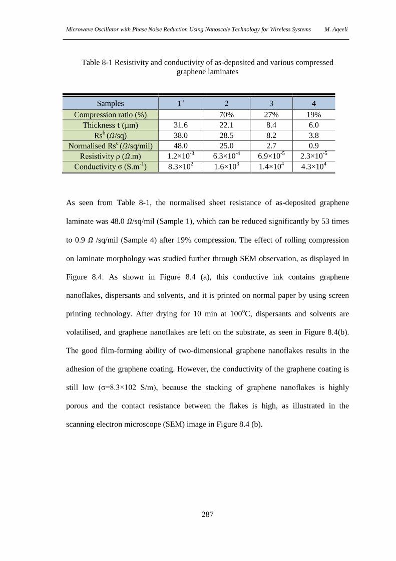
Microwave Oscillator with Phase Noise Reduction Using Nanoscale Technology for Wireless Systems M. Aqeeli
287
Table 8-1 Resistivity and conductivity of as-deposited and various compressed
graphene laminates
Samples 1a
2 3 4
Compression ratio (%)
70% 27% 19%
Thickness t (µm) 31.6 22.1 8.4 6.0
Rsb (𝛺/sq) 38.0 28.5 8.2 3.8
Normalised Rsc (𝛺/sq/mil) 48.0 25.0 2.7 0.9
Resistivity ρ (𝛺.m) 1.2×10⁻³
6.3×10⁻⁴
6.9×10⁻⁵
2.3×10⁻⁵
Conductivity σ (S.m-1
) 8.3×10² 1.6×10
3 1.4×10
4 4.3×10
4
As seen from Table 8-1, the normalised sheet resistance of as-deposited graphene
laminate was 48.0 𝛺/sq/mil (Sample 1), which can be reduced significantly by 53 times
to 0.9 𝛺 /sq/mil (Sample 4) after 19% compression. The effect of rolling compression
on laminate morphology was studied further through SEM observation, as displayed in
Figure 8.4. As shown in Figure 8.4 (a), this conductive ink contains graphene
nanoflakes, dispersants and solvents, and it is printed on normal paper by using screen
printing technology. After drying for 10 min at 100oC, dispersants and solvents are
volatilised, and graphene nanoflakes are left on the substrate, as seen in Figure 8.4(b).
The good film-forming ability of two-dimensional graphene nanoflakes results in the
adhesion of the graphene coating. However, the conductivity of the graphene coating is
still low (σ=8.3×10² S/m), because the stacking of graphene nanoflakes is highly
porous and the contact resistance between the flakes is high, as illustrated in the
scanning electron microscope (SEM) image in Figure 8.4 (b).
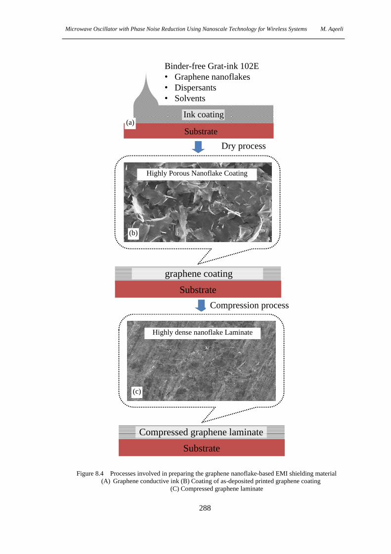
Microwave Oscillator with Phase Noise Reduction Using Nanoscale Technology for Wireless Systems M. Aqeeli
288
Substrate
Binder-free Grat-ink 102E
• Graphene nanoflakes
• Dispersants
• Solvents
Ink coating(a)
(b)
(c)
Substrate
Compressed graphene laminate
Highly dense nanoflake Laminate
Substrate
graphene coating
Highly Porous Nanoflake Coating
Dry process
Compression process
Figure 8.4 Processes involved in preparing the graphene nanoflake-based EMI shielding material
(A) Graphene conductive ink (B) Coating of as-deposited printed graphene coating
(C) Compressed graphene laminate
Microwave Oscillator with Phase Noise Reduction Using Nanoscale Technology for Wireless Systems M. Aqeeli
289
In order to increase conductivity, a rolling compression is applied to reduce contact
resistance and provide smooth pathways for electron transport. From the SEM in Figure
8.4 (c), a highly dense graphene nanoflake laminate forms, and this laminate is compact
and smooth. To illustrate the effect of compression, the conductivity and surface
impedance of the as-deposited graphene coating and the compressed graphene laminate
were compared. With a four-point probe measurement (RM3000, Jandel), the sheet
resistance of the as-deposited graphene coating was measured at 38.0 𝛺/sq, and the
thickness was 31.6 µm, as measured with a digital thickness gauge (PC-485, Teclock).
The bulk conductivity of the coating can be calculated at σ=8.3×10² S/m. However,
following compression, the thickness reduced to 6 µm, and sheet resistance was
Rs=3.8 𝛺/sq, which means, one-tenth of the un-compressed sample. Conductivity
increased to σ=0.43×10⁵ S/m, which reveals the compression procedure increases
conductivity 50-fold. In our previous work [162], this material was used for radio
frequency radiation. However, its superior properties as far as flexibility, lightweight,
high conductivity, environmental friendliness, etc. are concerned promise many more
potential applications. As this material is mechanically flexible and highly conductive,
and the preparation procedure is compatible with heat-sensitive materials such as paper,
plastics and textiles, to name a few, it is a strong candidate for EMI shielding, and
especially for wearable shielding applications. Herein, the potential applications of the
new EMI shielding material are experimentally explored. The EMI shielding material
samples printed on paper are displayed in Figure 8.5 (a), while Figure 8.5 (b)
demonstrates the flexibility of the samples when the same paper is bent. The sheet
resistance of these graphene laminates is measured at Rs=3 𝛺/sq and a thickness of
t=7.7 µm.

Microwave Oscillator with Phase Noise Reduction Using Nanoscale Technology for Wireless Systems M. Aqeeli
290
(c)
Coaxial-Waveguide
adapters
DUT
(d)
Vector Network
Analyser
(a) (b)
Figure 8.5 Graphene samples and measurement of SE in a waveguide system
(A) Printed on paper for DC measurement
(B) Printed on paper and bent to verify the ink graphene’s flexibility
(C) Graphene laminate attached to cover the waveguide port
(D) SE measurement based on the waveguide system

Microwave Oscillator with Phase Noise Reduction Using Nanoscale Technology for Wireless Systems M. Aqeeli
291
To measure the SE of the graphene laminate-based shielding material, the sample was
tailored to fit the size of the waveguide port (15.8 mm×7.9 mm) and was pasted to cover
the port, as seen in Figure 8.5 (c). The configuration of the test setup and measurements
is displayed in Figure 8.5 (d). Two waveguide-to-coaxial adapters are connected, to
measure the transmission (S21), using a vector network analyser (VNA), Agilent model
number N5230A. The graphene laminate sample (DUT, device under test) is inserted
between two waveguide ports, as highlighted in Figure 8.5 (c). Transmission – with and
without DUT – was recorded and is shown in Figure 8.6. As can be seen, when the
DUT is not inserted, the S21 is close to 0 dB, namely full transmission between two
VNA ports. However, when the DTU is placed, the transmission decreases dynamically
to below -35 dB to -40 dB in 12 GHz to18 GHz band.
12 13 14 15 16 17 18-50
-40
-30
-20
-10
0
Frequency (GHz)
S-P
aram
eter
s (d
B)
S21 (Without DUT)
S21 (With DUT)
Figure 8.6 Measured transmissions in a waveguide, with and without DUT

Microwave Oscillator with Phase Noise Reduction Using Nanoscale Technology for Wireless Systems M. Aqeeli
292
From the differences in transmission shown in Figure 8.7, the SE is calculated and
depicted in Figure 8.8. As shown, the SE is above 32 dB between 12 GHz and 18 GHz,
and at a central frequency of 15 GHz the SE sits at around 37 dB.
12 13 14 15 16 17 1825
30
35
40
45
Frequency (GHz)
102E
Sh
ield
ing
Eff
ecti
vn
ess
(dB
)
Figure 8.7 Shielding effectiveness of graphene laminate
As the thickness (7.7 µm) is less than half of the skin depth at 15 GHz (19.7 µm), the
SE can be further improved by increasing the thickness of the graphene laminate. From
the above analysis, it is demonstrated unambiguously that this lightweight,
mechanically flexible, graphene-based shielding material can provide effective
shielding against electromagnetic (EM) waves.

Microwave Oscillator with Phase Noise Reduction Using Nanoscale Technology for Wireless Systems M. Aqeeli
293
8.6: Chapter summary
This chapter has introduced highly conductive graphene laminate printed on paper with
the sophisticated advantages of being lightweight, flexible and low in cost. The
potential in providing effective EM wave shielding has been experimentally verified.
The advantages in flexibility, conductivity and thermal stability make graphene
laminate very promising in various applications, such as EM-shielding clothes and EMI
shielding for aerospace and wireless communication devices.

Microwave Oscillator with Phase Noise Reduction Using Nanoscale Technology for Wireless Systems M. Aqeeli
294
Conclusion Chapter 9:
and Future work
9.1: Conclusion
High-performance microwave oscillators are among the key building blocks required in
modern wireless communication systems. Compact VCOs that provide wide tuning
ranges, low phase noise variation and low power consumption are highly sought after
for GSM/WCDMA/LTE frequency synthesisers in modern, multi-standard transceivers.
The demand for electronic devices of reduced size, low power consumption and low-
cost is currently the highest it has ever been. Single-chip silicon-based VCOs are one of
the most pervasive and attractive of the innovations emerging in wireless
communication applications. However, phase noise variations still continue to exert
significant influence on the performance limits of all silicon-based microwave device
implementations. Therefore, this work has focused on phase noise as a dominant loss
factor in LC tanks. Furthermore, the design optimisation of VCOs was carried out from
Microwave Oscillator with Phase Noise Reduction Using Nanoscale Technology for Wireless Systems M. Aqeeli
295
a high-quality varactor perspective. Three silicon-based VCOs with wide tuning range
and low phase noise variations were presented in this thesis. Finally, a summary of the
contributions of this thesis is given below.
1. The advantages of a digital varactor switching array which has been
implemented into a wideband CMOS VCO for 5 GHz WiMAX/WLAN
applications have been verified analytically and simulated accordingly. As proof
of the concept, the performances of the three novel VCOs presented in this study
are compared to other state-of-the-art designs in several CMOS technologies,
with the results showing clearly that the achieved designs are the best in terms of
phase noise, power dissipation, bandwidth and FoM, not only for fabricated
work, but also for simulated designs. In this thesis, the phase noise of high-
frequency VCOs has been studied extensively. The analysis and design of a
novel FoM, low-phase noise, LC tank voltage-controlled oscillator (VCO) has
been presented. The new design decreases phase noise and optimises the FoM.
The work also presents a fully integrated 5.0 GHz VCO, designed and simulated
using 130-nm CMOS technology. Instead of using a conventional diode-based
varactor in the tank design, a high-performance metal-oxide-metal (MOM)
capacitor varactor bank is implemented as an effective varactor. A wideband
LC-VCO has been designed and simulated to meet WiMAX/WLAN
specification and the most stringent phase noise requirements. An ideal VCO
has a broadband tuning range of approximately 56 percent which varies linearly
with the control voltage. The high performance VCO specifications include
simulated phase noise of -133.8 dBc/Hz at an offset frequency of 1 MHz away

Microwave Oscillator with Phase Noise Reduction Using Nanoscale Technology for Wireless Systems M. Aqeeli
296
from the 5.0 GHz FoM of -203.5 dBc/Hz, while the VCO core’s total power
consumption is 3.2 mW from a 1.2 V supply voltage.
2. A new oscillator with low phase noise is based on an LH metamaterial bandpass
filter embedded into the feedback loop of the oscillator. An LH microstrip filter-
based oscillator is proposed, at the complex quality factor Qsc-peak frequency.
The test results show clearly that the phase noise of the oscillator designed at
Qsc-peak frequency can be significantly reduced; in fact, phase noise improved
by more than 1 dB compared to a combline filter resonator. The proposed
oscillator’s measured results at the centre frequency demonstrate a phase noise
of -142.3 dBc/Hz and an FoM of -201.13 dBc/Hz at a 1 MHz frequency offset,
less than -32 dBm spurious harmonics and total oscillator power consumption of
3.0 mW from a 3.2V supply voltage.
3. With the rapid development of the integrated circuits (ICs) design, there are
increasing demands for electromagnetic compatibility performance in wireless
communication systems, in which the electromagnetic compatibility
performance of VCO devices is crucial to the design process of the entire
system. Therefore, this research extends the potential of highly flexible and
conductive graphene laminate to the application of electromagnetic interference
(EMI) shielding. Graphene nanoflake-based conductive ink is printed on paper
and compressed to form graphene laminate with a conductivity of 0.43×10⁵
S/m. Shielding effectiveness was shown experimentally to be above 32 dB when
between 12 GHz and 18 GHz, even though its thickness was only 7.7 µm. This
result demonstrates that graphene has great potential in offering lightweight,
Microwave Oscillator with Phase Noise Reduction Using Nanoscale Technology for Wireless Systems M. Aqeeli
297
low-cost, flexible and environmentally friendly shielding materials which can be
extended to offers the require shielding from electromagnetic interference (EMI)
of not only VCOs phase noise optimisation but for sensitive electronic devices
as well.
9.2: Future research opportunities
While the research outcome is promising in terms of high-specification VCO design,
further research is required, mainly to improve the design and related components.
1. This paper focuses on high-performance LC CMOS VCO design at 5 GHz
implementing a centre-tapped symmetric inductor designed using 130 nm 1P8M
RF CMOS process inductors which have a low quality-factors ranging from
10 to 20. The effects of the inductor Q-factor on the VCO performance should
be investigated and analyzed from the phase noise perspective.
2. In addition, a varactor may be attached on the CRLH-TL resonator of the filter
to control the oscillation frequency the developed oscillator and can be easily
extended to a VCO.
3. An experimental study for the purposed electromagnetic interference shielding
based on highly conductive graphene laminate presented in chapter 8 to analyze
the disturbing effects of low and high power EMI on first a VCO, and then, on a
PLL phase noise.

Microwave Oscillator with Phase Noise Reduction Using Nanoscale Technology for Wireless Systems M. Aqeeli
298
4. The current biasing circuit is a major noise source and contributes to phase noise
in VCOs. Therefore, biasing filtering techniques are important parameters which
need to be investigated. Solutions such as dynamic bias filtering is
recommended for fast VCO start-up, and it is necessary to explore passive
components which are used to form some of the LC tank of the VCO.
Microwave Oscillator with Phase Noise Reduction Using Nanoscale Technology for Wireless Systems M. Aqeeli
299
List of publications
1. Mohammed Aqeeli, Ting Leng, Xianjun Huang *, Jia Cing Chen, Kuo Hsin
Chang, Abdullah Alburaikan and Zhirun Hu., " Electromagnetic Interference
Shielding Based on Highly Flexible and Conductive Graphene Laminate", The
Institution of Engineering and Technology (IET) Electronics Letters, Issue 16,
published on August 2015.
2. Xianjun Huang,1 Ting Leng, Mengjian Zhu, Xiao Zhang, JiaCing Chen,
KuoHsin Chang, Mohammed Aqeeli, Andre K. Geim, Kostya S. Novoselov,
Zhirun Hu, " Highly Flexible and Conductive Printed Graphene for Wireless
Wearable Communications Applications", Accepted in the Scientific Reports,
2015.
3. A. Alburaikan, M. Aqeeli, X. Huang, Z. Hu, " Low Phase Noise Free-running
Oscillator Based on High Selectivity Bandpass Filter Using Composite
Right/Left-Handed Transmission Line", Accepted to IEEE Microwave and
Wireless Components Letters, 2015.
4. M. Aqeeli, A. Alburaikan, X. Huang, Z. Hu, "Wide Tuning Range Voltage
Controlled Oscillator (VCO) with Minimized Phase Noise Variation in
Nanoscale CMOS Technology", the International IEEE Conference on
Nanotechnology, IEEE NANO 2015.
5. M. Aqeeli, A. Alburaikan, C. Muvianto, X. Huang, Z. Hu "Wideband Gain
Linearized Microwave Voltage Controlled Oscillator with Low Phase Noise
Variation in Nanometer CMOS Technology" Journal of circuits, systems and
computers, Vol. 24, No 3,pp. 1-14, 2015.
6. M. Aqeeli, A. Alburaikan, X. Huang, Z. Hu, " Low-Phase Noise Variation VCO
Implementing Resistorless, " IEEE International Conference on Integrated
Circuit Design and Technology (ICICDT), 2015.
7. M. Aqeeli, A. Alburaikan, X. Huang, Z. Hu, " Low-Phase Noise Variation and
Gain linearized VCO Implementing Digital Varator Arrays", Accepted on the
22nd European conference on circuit theory and design, ECCTD 2015.

Microwave Oscillator with Phase Noise Reduction Using Nanoscale Technology for Wireless Systems M. Aqeeli
300
8. Xianjun Huang, Xiao Zhang, Zhirun Hu, Aqeeli Mohammed, Alburaikan
Abdullah, " Design of broadband and tunable terahertz absorbers based on
graphene metasurface: equivalent circuit model approach" IET Microwaves
Antennas & Propagation, Vol. 9, No 4,pp. 307-312, 2015.
9. A. Alburaikan, M. Aqeeli, X. Huang, Z. Hu "Miniaturized ultra-wideband
bandpass filter based on CRLH-TL unit cell "44th European Microwave
Conference (EuMC), pp. 540-543, 2015.
10. A. Alburaikan, M. Aqeeli, X. Huang, Z. Hu "Miniaturized Via-less ultra-
wideband bandpass filter based on CRLH-TL unit cell "IEEE Radio wireless
Week, 2015.
11. M. Aqeeli, A. Alburaikan, C. Muvianto, X. Huang, Z. Hu " An Ultra-Wideband
and Low Phase Noise CMOS VCO for WiMAX/WLAN using a Novel Metal-
Oxide-Metal Digital Capacitor Switching Array " IET Circuits, Devices &
Systems, provisionally accepted.
12. M. Aqeeli, A. Alburaikan, C. Muvianto, X. Huang, Z. Hu "An Ultra-Wideband
and Gain Linearized CMOS VCO with Minor Phase Noise Variation " European
Microwave Association, IEEE Asia Pacific Microwave Conference (APMC),
pp. 965-967, 2014.
13. M. Aqeeli, A. Alburaikan, C. Muvianto, X. Huang, Z. Hu "A Novel Wide
Tuning Range LC-VCO with Small Phase Noise Variation " The IEEE 11th
Vehicular Technology Society Asia Pacific Wireless Communications
Symposium ( IEEE VTS APWCS), 2014.
14. M. Aqeeli, Z. Hu, X. Huang, A. Alburaikan, and C. Muvianto "An Ultra-
wideband and Low Phase Noise LC-VCO Using nMOS Varactor with MOM
Digital Capacitor Switching Arrays" 35th
Progress In Electromagnetics Research
Symposium, pp. 386-389, 2014.
15. M. Aqeeli, Z. Hu, X. Huang, A. Alburaikan, C. Muvianto "Low-Power and
Wideband LC-VCO for WiMAX in CMOS Technology" IEEE UKSim-AMSS
16th International Conference on Computer Modelling and Simulation, pp. 553-
557, 2014.
16. X. Huang, Z. Hu, X. Zhang, M. Abdalla, T. leng, M. Aqeeli, A. Alburaikan, "
Tuneable Microwave CPW Antenna with Graphene Sheet " 2014 Loughborough
Antennas & Propagation Conference (LAPC).

Microwave Oscillator with Phase Noise Reduction Using Nanoscale Technology for Wireless Systems M. Aqeeli
301
17. M. Aqeeli, Zhirun Hu, Cahyo Muvianto, " Design of a Novel 6.68 GHz Low-
Phase-Noise VCO Adopting Metal-Oxide-Metal Capacitors Using 130nm
CMOS Technology" the IEEE Electron Devices Poster Conference, 2013.
18. M. Aqeeli and H. Zhirun, “Design of a high performance 5.2 GHz low phase
noise 90nm CMOS voltage controlled oscillator,” Proceedings of the 2nd
International Conference on Computer Science and Electronics Engineering
(ICCSEE), Atlantis Press, 2013, pp. 715-719,2013.
19. M. Aqeeli, Zhirun Hu, Cahyo Muvianto, " A 6.72 GHz Low-Phase-Noise
Voltage Controlled Oscillator Adopting Metal-Oxide-Metal Capacitors Using
130nm CMOS Technology" the 2013 Fifth International Conference on
Computational Intelligence, Communication Systems and Networks, pp. 101 –
106, 2013.
20. M. Aqeeli and Z. Hu, " Design of a High Performance 5.0 GHz Low Phase
Noise 0.35μm CMOS Voltage Controlled Oscillator " the International Journal
of Information and Electronics Engineering, IJIEE, Vol. 3, No. 4, pp. 436-439,
2013.

Microwave Oscillator with Phase Noise Reduction Using Nanoscale Technology for Wireless Systems M. Aqeeli
302
REFERENCES
[1] A. Ismail, "CMOS PLLs and VCOs for 4G Wireless," ed: Kluwer Academic
Publishers, Norwell, 2004.
[2] K. Shu and E. Sánchez-Sinencio, CMOS PLL Synthesizers: Analysis and
Design: Analysis and Design vol. 783: Springer Science & Business Media,
2006.
[3] T. Ernst, L. Duraffourg, C. Dupre, E. Bernard, P. Andreucci, S. Bécu, et al.,
"Novel Si-based nanowire devices: Will they serve ultimate MOSFETs scaling
or ultimate hybrid integration?," in 2008 IEEE International Electron Devices
Meeting, 2008.
[4] R. Mukhopadhyay, Y. Park, P. Sen, N. Srirattana, J. Lee, C.-H. Lee, et al.,
"Reconfigurable RFICs in Si-based technologies for a compact intelligent RF
front-end," Microwave Theory and Techniques, IEEE Transactions on, vol. 53,
pp. 81-93, 2005.
[5] H. S. Bennett, R. Brederlow, J. C. Costa, P. E. Cottrell, W. M. Huang, A.
Immorlica, et al., "Device and technology evolution for Si-based RF integrated
circuits," Electron Devices, IEEE Transactions on, vol. 52, pp. 1235-1258,
2005.
[6] R. Caverly, CMOS RFIC design principles: Artech House, Inc., 2007.
[7] G. Huang, S.-K. Kim, Z. Gao, S. Kim, V. Fusco, and B.-S. Kim, "A 45 GHz
CMOS VCO Adopting Digitally Switchable Metal-Oxide-Metal Capacitors,"
Microwave and Wireless Components Letters, IEEE, vol. 21, pp. 270-272, 2011.
[8] F. Maloberti, ANALOG DESIGN FOR CMOS VLSI SYSTEMS. USA: Kluwer
Academic, 2003.
Microwave Oscillator with Phase Noise Reduction Using Nanoscale Technology for Wireless Systems M. Aqeeli
303
[9] L. B. Oliveira, Analysis and Design of Quadrature Oscillators. Dordrecht:
Dordrecht : Springer, 2008.
[10] W. M. Sansen, Analog design essentials vol. 859: Springer Science & Business
Media, 2007.
[11] A. Bellaouar and M. Elmasry, Low-power digital VLSI design: circuits and
systems: Springer Science & Business Media, 2012.
[12] M. Tiebout, Low Power VCO Design in CMOS. Dordrecht
Berlin, Heidelberg: Dordrecht : Springer-Verlag Berlin and Heidelberg GmbH & Co.
KG, 2006.
[13] S. Yoder, M. Ismail, and W. Khalil, VCO-based Quantizers Using Frequency-
to-digital and Time-to-digital Converters: Springer, 2011.
[14] M. Aqeeli, A. Alburaikan, C. Muvianto, X. Huang, and Z. Hu, "A Wideband
Gain Linearized Microwave Voltage Controlled Oscillator with Low Phase
Noise Variation in Nanometer CMOS Technology," Journal of Circuits, Systems
and Computers, vol. 24, p. 1550024, 2015.
[15] R. E. Best, Phase locked loops: McGraw-Hill Professional, 2007.
[16] T. H. Lee and A. Hajimiri, "Oscillator phase noise: a tutorial," Solid-State
Circuits, IEEE Journal of, vol. 35, pp. 326-336, 2000.
[17] M. del Mar Hershenson, A. Hajimiri, S. S. Mohan, S. P. Boyd, and T. H. Lee,
"Design and optimization of LC oscillators," in Proceedings of the 1999
IEEE/ACM international conference on Computer-aided design, 1999, pp. 65-
69.
[18] A. Hajimiri and T. H. Lee, "Design issues in CMOS differential LC oscillators,"
Solid-State Circuits, IEEE Journal of, vol. 34, pp. 717-724, 1999.

Microwave Oscillator with Phase Noise Reduction Using Nanoscale Technology for Wireless Systems M. Aqeeli
304
[19] D. Ham and A. Hajimiri, "Concepts and methods in optimization of integrated
LC VCOs," Solid-State Circuits, IEEE Journal of, vol. 36, pp. 896-909, 2001.
[20] D. B. Leeson, "A simple model of feedback oscillator noise spectrum,"
Proceedings of the IEEE, vol. 54, pp. 329-330, 1966.
[21] A. Hajimiri and T. H. Lee, "A general theory of phase noise in electrical
oscillators," Solid-State Circuits, IEEE Journal of, vol. 33, pp. 179-194, 1998.
[22] A. Hajimiri and T. H. Lee, The design of low noise oscillators: Springer Science
& Business Media, 1999.
[23] A. Hajimiri, S. Limotyrakis, and T. H. Lee, "Jitter and phase noise in ring
oscillators," Solid-State Circuits, IEEE Journal of, vol. 34, pp. 790-804, 1999.
[24] B. Razavi, RF microelectronics vol. 1: Prentice Hall New Jersey, 1998.
[25] M. Aqeeli, A. Alburaikan, C. Muvianto, X. Huang, and Z. Hu, "An ultra-
wideband and gain linearized CMOS VCO with minor phase noise variation," in
Microwave Conference (APMC), 2014 Asia-Pacific, 2014, pp. 965-967.
[26] I. Gutierrez, J. Meléndez, and E. Hernández, Design and characterization of
integrated varactors for RF applications: John Wiley & Sons, 2007.
[27] A. Grebennikov, "CMOS Voltage‐Controlled Oscillators," RF and Microwave
Transistor Oscillator Design, pp. 299-345, 2007.
[28] A. L. Lacaita, S. Levantino, and C. Samori, Integrated frequency synthesizers
for wireless systems: Cambridge University Press, 2007.
[29] G. Bianchi, Phase-locked loop synthesizer simulation: McGraw-Hill, Inc., 2005.
[30] D. Banerjee, PLL performance, simulation and design: Dog Ear Publishing,
2006.
[31] T. Dubois, J. J. Laurin, J. Raoult, and S. Jarrix, "Effect of Low and High Power
Continuous Wave Electromagnetic Interference on a Microwave Oscillator
Microwave Oscillator with Phase Noise Reduction Using Nanoscale Technology for Wireless Systems M. Aqeeli
305
System: From VCO to PLL to QPSK Receiver," Electromagnetic Compatibility,
IEEE Transactions on, vol. 56, pp. 286-293, 2014.
[32] C. Jian, F. Jonsson, H. Olsson, Z. Li-Rong, and Z. Dian, "A current shaping
technique to lower phase noise in LC oscillators," in Electronics, Circuits and
Systems, 2008. ICECS 2008. 15th IEEE International Conference on, 2008, pp.
392-395.
[33] E. Hegazi, The Designer's Guide to High-Purity Oscillators. Dordrecht:
Dordrecht : Springer, 2006.
[34] R. J. van de Plassche, J. Huijsing, and W. Sansen, Analog circuit design: RF
analog-to-digital converters; sensor and actuator interfaces; low-noise
oscillators, PLLs and synthesizers: Springer Science & Business Media, 2013.
[35] J. Héctor, C. Sturm, and J. Ponte, Radio Systems Engineering: A Tutorial
Approach: Springer, 2014.
[36] Q. Zou, A. Tarighat, and A. H. Sayed, "Compensation of phase noise in OFDM
wireless systems," Signal Processing, IEEE Transactions on, vol. 55, pp. 5407-
5424, 2007.
[37] L. Piazzo and P. Mandarini, "Analysis of phase noise effects in OFDM
modems," Communications, IEEE Transactions on, vol. 50, pp. 1696-1705,
2002.
[38] G. Szczepkowski, "Analysis and design of wideband voltage controlled
oscillators using self-oscillating active inductors," PhD, Department of
Electronic Engineering, University of Ireland, 2010.
[39] E. Hegazi, The Designer's Guide to High-Purity Oscillators. Dordrecht:
Dordrecht : Springer, 2006.
Microwave Oscillator with Phase Noise Reduction Using Nanoscale Technology for Wireless Systems M. Aqeeli
306
[40] M. Nick, "New Q-Enhanced Planar Resonators for Low Phase-Noise Radio
Frequency Oscillators," The University of Michigan, 2011.
[41] U. L. Rohde, A. K. Poddar, and G. Böck, The design of modern microwave
oscillators for wireless applications: theory and optimization: John Wiley &
Sons, 2005.
[42] K. Yao, F. Lorenzelli, and C.-E. Chen, Detection and Estimation for
Communication and Radar Systems: Cambridge University Press, 2013.
[43] W. P. Robins, Phase noise in signal sources: theory and applications vol. 9:
IET, 1984.
[44] F. Yuan, CMOS active inductors and transformers: principle, implementation,
and applications: Springer Science & Business Media, 2008.
[45] N. Yanay and E. Socher, "Wide Tuning-Range mm-Wave Voltage-Controlled
Oscillator Employing an Artificial Magnetic Transmission Line," Microwave
Theory and Techniques, IEEE Transactions on, vol. 63, pp. 1342-1352, 2015.
[46] J. Zhang, N. Sharma, W. Choi, D. Shim, and Q. Zhong, "85-to-127 GHz CMOS
Signal Generation Using a Quadrature VCO With Passive Coupling and
Broadband Harmonic Combining for Rotational Spectroscopy," 2015.
[47] J. McNeill, R. Majidi, and J. Gong, "“Split ADC” Background Linearization of
VCO-Based ADCs," Circuits and Systems I: Regular Papers, IEEE
Transactions on, vol. 62, pp. 49-58, 2015.
[48] A. Buonomo and A. Lo Schiavo, "Analysis and Design of Dual-Mode CMOS
LC-VCOs," Circuits and Systems I: Regular Papers, IEEE Transactions on, vol.
62, pp. 1845-1853, 2015.

Microwave Oscillator with Phase Noise Reduction Using Nanoscale Technology for Wireless Systems M. Aqeeli
307
[49] M.-H. Shen and P.-C. Huang, "A Wide-Range Multiport LC-Ladder Oscillator
and Its Applications to a 1.2–10.1 GHz PLL," Very Large Scale Integration
(VLSI) Systems, IEEE Transactions on, vol. 23, pp. 184-188, 2015.
[50] J. Park, H. Ryu, K.-W. Ha, J.-G. Kim, and D. Baek, "76–81-GHz CMOS
Transmitter With a Phase-Locked-Loop-Based Multichirp Modulator for
Automotive Radar," Microwave Theory and Techniques, IEEE Transactions on,
vol. 63, pp. 1399-1408, 2015.
[51] K.-C. Lu, F.-K. Wang, and T.-S. Horng, "Ultralow phase noise and wideband
CMOS VCO using symmetrical body-bias PMOS varactors," Microwave and
Wireless Components Letters, IEEE, vol. 23, pp. 90-92, 2013.
[52] T. Xin, H. Fengyi, T. Xusheng, and S. Mingchi, "A wideband 0.13 μm CMOS
LC-VCO for IMT-advanced and UWB applications," Journal of
Semiconductors, vol. 34, p. 015004, 2013.
[53] M. Aqeeli, H. Zhirun, and C. Muvianto, "A Novel 6.72GHz Low Phase Noise
Voltage-Controlled Oscillator Adopting Metal-Oxide-Metal Capacitors Using
130nm CMOS Technology," in Computational Intelligence, Communication
Systems and Networks (CICSyN), 2013 Fifth International Conference on, 2013,
pp. 101-106.
[54] S. H. Voldman, ESD: circuits and devices: John Wiley & Sons, 2015.
[55] K. Zhang, S. Cheng, X. Zhou, W. Li, and R. Liu, "A wide band differentially
switch-tuned CMOS monolithic quadrature VCO with a low Kvco and high
linearity," Microelectronics Journal, vol. 40, pp. 881-886, 2009.
[56] Z. Wang, M. J. Deen, and A. Rahal, "Modeling of integrated inductors and
resistors for microwave applications," Integrated passive component technology,
pp. 247-291, 2003.
Microwave Oscillator with Phase Noise Reduction Using Nanoscale Technology for Wireless Systems M. Aqeeli
308
[57] R. L. Bunch, D. Sanderson, and S. Raman, "Quality factor and inductance in
differential IC implementations," Microwave Magazine, IEEE, vol. 3, pp. 82-92,
2002.
[58] J. N. Burghartz, D. Edelstein, M. Soyuer, H. Ainspan, and K. Jenkins, "RF
circuit design aspects of spiral inductors on silicon," Solid-State Circuits, IEEE
Journal of, vol. 33, pp. 2028-2034, 1998.
[59] Y. K. Koutsoyannopoulos and Y. Papananos, "Systematic analysis and modeling
of integrated inductors and transformers in RF IC design," Circuits and Systems
II: Analog and Digital Signal Processing, IEEE Transactions on, vol. 47, pp.
699-713, 2000.
[60] A. Asenov, S. Roy, R. Brown, G. Roy, C. Alexander, C. Riddet, et al.,
"Advanced simulation of statistical variability and reliability in nano CMOS
transistors," in Electron Devices Meeting, 2008. IEDM 2008. IEEE
International, 2008, pp. 1-1.
[61] E. K. Blum and A. V. Aho, Computer Science: The Hardware, Software and
Heart of it: Springer Science & Business Media, 2011.
[62] R. J. Baker, CMOS: circuit design, layout, and simulation vol. 18: John Wiley &
Sons, 2011.
[63] V. Kursun and E. G. Friedman, Multi-voltage CMOS circuit design: John Wiley
& Sons, 2006.
[64] F. Maloberti, "Resistors, Capacitors, Switches," Analog Design for CMOS VLSI
Systems, pp. 59-98, 2003.
[65] I. n. i. Gutierrez, Design and characterization of integrated varactors for RF
applications / Inigo Gutierrez, Juan Melendez, Erik Hernandez. Chichester,

Microwave Oscillator with Phase Noise Reduction Using Nanoscale Technology for Wireless Systems M. Aqeeli
309
West Sussex, England ; Hoboken, NJ: Chichester, West Sussex, England ;
Hoboken, NJ : Wiley, 2006.
[66] Í. Gutiérrez, J. Meléndez, and E. Hernández, "MOS Varactors," Design and
Characterization of Integrated Varactors for RF Applications, pp. 31-52, 2006.
[67] E. Brunvand, Digital VLSI chip design with Cadence and Synopsys CAD tools:
Addison-Wesley, 2010.
[68] V. A. Chandrasetty, "Analog and Mixed Signal Design," in VLSI Design, ed:
Springer, 2011, pp. 83-104.
[69] J. Maget, M. Tiebout, and R. Kraus, "MOS varactors with n- and p-type gates
and their influence on an LC-VCO in digital CMOS," Solid-State Circuits, IEEE
Journal of, vol. 38, pp. 1139-1147, 2003.
[70] N. Weste, D. Harris, and A. Banerjee, "Cmos vlsi design," A circuits and
systems perspective, vol. 11, p. 739, 2005.
[71] C. Nguyen, "Fundamentals of CMOS Transistors for RFIC Design," Radio-
Frequency Integrated-Circuit Engineering, pp. 379-417.
[72] J. Jing, Y. Xiaopeng, L. Xiaoming, L. Wei Meng, and Z. Jianjun, "A Wideband
Voltage-Controlled Oscillator With Gain Linearized Varactor Bank,"
Components, Packaging and Manufacturing Technology, IEEE Transactions on,
vol. 4, pp. 905-910, 2014.
[73] L. Fanori and P. Andreani, "Class-D CMOS Oscillators," Solid-State Circuits,
IEEE Journal of, vol. 48, pp. 3105-3119, 2013.
[74] T. Seong, J. J. Kim, and J. Choi, "Analysis and Design of a Core-Size-Scalable
Low Phase Noise-VCO for Multi-Standard Cellular Transceivers," Circuits and
Systems I: Regular Papers, IEEE Transactions on, vol. 62, pp. 781-790, 2015.
[75] F. M. Gardner, Phaselock techniques: John Wiley & Sons, 2005.
Microwave Oscillator with Phase Noise Reduction Using Nanoscale Technology for Wireless Systems M. Aqeeli
310
[76] L. Kuan-Chung, W. Fu-Kang, and H. Tzyy-Sheng, "Ultralow Phase Noise and
Wideband CMOS VCO Using Symmetrical Body-Bias PMOS Varactors,"
Microwave and Wireless Components Letters, IEEE, vol. 23, pp. 90-92, 2013.
[77] L. Dai and R. Harjani, Design of High-Performance CMOS Voltage-Controlled
Oscillators vol. 708: Springer Science & Business Media, 2012.
[78] Y. Xizhen, M. Chengyan, Y. Tianchun, X. Shimao, and J. Yuhua, "A low-phase-
noise LC-VCO with an enhanced-Q varactor for use in a high-sensitivity GNSS
receiver," Journal of Semiconductors, vol. 33, p. 055002, 2012.
[79] F. Pepe, A. Bonfanti, S. Levantino, C. Samori, and A. L. Lacaita, "A wideband
voltage-biased LC oscillator with reduced flicker noise up-conversion," in Radio
Frequency Integrated Circuits Symposium (RFIC), 2013 IEEE, 2013, pp. 27-30.
[80] J. P. Uyemura, Chip design for submicron VLSI: CMOS layout and simulation:
Thomson New York, 2006.
[81] P. Andreani, K. Kozmin, P. Sandrup, M. Nilsson, and T. Mattsson, "A TX VCO
for WCDMA/EDGE in 90 nm RF CMOS," Solid-State Circuits, IEEE Journal
of, vol. 46, pp. 1618-1626, 2011.
[82] F. Yuan, "A fully differential VCO cell with active inductors for Gbps serial
links," Analog Integrated Circuits and Signal Processing, vol. 47, pp. 213-223,
2006.
[83] M. Aqeeli, H. Zhirun, H. Xianjun, A. Alburaikan, and C. Muvianto, "Low-
Power and Wideband LC-VCO for WiMAX in CMOS Technology," in
Computer Modelling and Simulation (UKSim), 2014 UKSim-AMSS 16th
International Conference on, 2014, pp. 553-557.
[84] A. Mohammed, A. Abdullah, H. Xianjun, and H. Zhirun, "Low-Phase noise
Variation VCO Imlpementing Resistoless Digitally controlled Varactor,"
Microwave Oscillator with Phase Noise Reduction Using Nanoscale Technology for Wireless Systems M. Aqeeli
311
presented at the 2015 IEEE International Conference on Integrated Circuit
Design and Technology (ICICDT), 2015.
[85] A. Mohammed, A. Abdullah, H. Xianjun, and H. Zhirun, "Wide Tuning Range
Voltage Controlled Oscillator (VCO) with Minimum Phase Noise Variation in
Nanoscale CMOS Technology," presented at the The International IEEE
Conference in Nanotechnology, 2015.
[86] M. Babaie and R. B. Staszewski, "An Ultra-Low Phase Noise Class-F 2 CMOS
Oscillator With 191 dBc/Hz FoM and Long-Term Reliability," Solid-State
Circuits, IEEE Journal of, vol. 50, pp. 679-692, 2015.
[87] P. Ruippo, T. A. Lehtonen, and N. T. Tchamov, "An UMTS and GSM Low
Phase Noise Inductively Tuned LC VCO," Microwave and Wireless
Components Letters, IEEE, vol. 20, pp. 163-165, 2010.
[88] M.-T. Hsu, A.-C. Ou, and R.-W. Jhong, "Implementation of 5GHz current-
reused VCO with linearity," in Microwave Conference (APMC), 2014 Asia-
Pacific, 2014, pp. 968-970.
[89] K.-C. Kuo and C.-W. Wu, "A low phase noise VCO for 5-GHz WiMAX/WLAN
frequency synthesizer," in Electron Devices and Solid-State Circuits (EDSSC),
2013 IEEE International Conference of, 2013, pp. 1-2.
[90] W. Muh-Dey, C. Sheng-Fuh, Z. Ye, Y. Yung-Jhih, and R. Negra, "2.4 GHz / 3.5
GHz dual-band wide-tuning-range quadrature VCO using harmonic-injection
coupling technique," in Silicon Monolithic Integrated Circuits in Rf Systems
(SiRF), 2014 IEEE 14th Topical Meeting on, 2014, pp. 107-109.
[91] L. Fanori and P. Andreani, "Highly Efficient Class-C CMOS VCOs, Including a
Comparison With Class-B VCOs," Solid-State Circuits, IEEE Journal of, vol.
48, pp. 1730-1740, 2013.

Microwave Oscillator with Phase Noise Reduction Using Nanoscale Technology for Wireless Systems M. Aqeeli
312
[92] J. G. Atallah and M. Ismail, Integrated frequency synthesis for convergent
wireless solutions: Springer Science & Business Media, 2012.
[93] I. Koffman and V. Roman, "Broadband wireless access solutions based on
OFDM access in IEEE 802.16," Communications Magazine, IEEE, vol. 40, pp.
96-103, 2002.
[94] C. Cicconetti, L. Lenzini, E. Mingozzi, and C. Eklund, "Quality of service
support in IEEE 802.16 networks," Network, IEEE, vol. 20, pp. 50-55, 2006.
[95] C. Caloz, Electromagnetic metamaterials : transmission line theory and
microwave applications : the engineering approach / Christophe Caloz, Tatsuo
Itoh. Hoboken, N.J.: Hoboken, N.J. : Wiley-Interscience, 2006.
[96] D. Smith and R. Liu, "Metamaterials: theory, design, and applications," ed:
Springer, New York, 2010.
[97] S. Zouhdi, A. Sihvola, and A. P. Vinogradov, Metamaterials and Plasmonics:
Fundamentals, Modelling, Applications: Springer Science & Business Media,
2008.
[98] J. B. Pendry, A. J. Holden, D. J. Robbins, and W. J. Stewart, "Magnetism from
conductors and enhanced nonlinear phenomena," Microwave Theory and
Techniques, IEEE Transactions on, vol. 47, pp. 2075-2084, 1999.
[99] R. A. Shelby, D. R. Smith, and S. Schultz, "Experimental Verification of a
Negative Index of Refraction," Science, vol. 292, pp. 77-79, 2001.
[100] C. Caloz and T. Itoh, "Transmission line approach of left-handed (LH) materials
and microstrip implementation of an artificial LH transmission line," Antennas
and Propagation, IEEE Transactions on, vol. 52, pp. 1159-1166, 2004.

Microwave Oscillator with Phase Noise Reduction Using Nanoscale Technology for Wireless Systems M. Aqeeli
313
[101] A. Sanada, K. Murakami, S. Aso, H. Kubo, and I. Awai, "A via-free microstrip
left-handed transmission line," in Microwave Symposium Digest, 2004 IEEE
MTT-S International, 2004, pp. 301-304 Vol.1.
[102] V. Mishra, R. K. Chaudhary, K. V. Srivastava, and A. Biswas, "Compact two
pole bandpass filter implemented using via-free composite right/left handed
transmission line with radial stubs," in Microwave Conference (EuMC), 2011
41st European, 2011, pp. 571-574.
[103] S. Kahng and J. Ju, "Design of the UWB bandpass filter based on the 1 cell of
microstrip CRLH-TL," in Microwave and Millimeter Wave Technology, 2008.
ICMMT 2008. International Conference on, 2008, pp. 69-72.
[104] D. Decle Colin and Z. Hu, "Novel CSRR-loaded left handed microstrip
transmission line, for microwave applications," presented at the IEEE
International Symposium on Antennas and Propagation, 2013.
[105] K. Aydin, I. Bulu, and E. Ozbay, "Electromagnetic wave focusing from sources
inside a two-dimensional left-handed material superlens," New Journal of
Physics, vol. 8, p. 221, 2006.
[106] C. Jaewon and S. Chulhun, "Microstrip Square Open-Loop Multiple Split-Ring
Resonator for Low-Phase-Noise VCO," Microwave Theory and Techniques,
IEEE Transactions on, vol. 56, pp. 3245-3252, 2008.
[107] S. Karimian, "Metamaterial Stepped Impedance Resonator Filters for Wireless
Communication Systems," 2011.
[108] F. Hirtenfelder, "Effective Antenna Simulations using CST MICROWAVE
STUDIO®," in Antennas, 2007. INICA '07. 2nd International ITG Conference
on, 2007, pp. 239-239.

Microwave Oscillator with Phase Noise Reduction Using Nanoscale Technology for Wireless Systems M. Aqeeli
314
[109] A. M. e. Anile, Scientific Computing in Electrical Engineering / edited by
Angelo Marcello Anile, Giuseppe Alì, Giovanni Mascali: Berlin, Heidelberg :
Springer Berlin Heidelberg, 2006.
[110] G. V. Viktor, "The electrodynamics of substances with simultaneously negative
values of and," vol. 10, ed, 1968, pp. 509-514.
[111] D. R. Smith, D. C. Vier, N. Kroll, and S. Schultz, "Direct calculation of
permeability and permittivity for a left-handed metamaterial," Applied Physics
Letters, vol. 77, p. 2246, 2000.
[112] C. Caloz and T. Itoh, "Application of the transmission line theory of left-handed
(LH) materials to the realization of a microstrip "LH line"," in Antennas and
Propagation Society International Symposium, 2002. IEEE, 2002, pp. 412-415
vol.2.
[113] C. Caloz and T. Itoh, "Novel microwave devices and structures based on the
transmission line approach of meta-materials," in Microwave Symposium Digest,
2003 IEEE MTT-S International, 2003, pp. 195-198 vol.1.
[114] J. Bonache, F. Martin, F. Falcone, J. Garcia, I. Gil, T. Lopetegi, et al., "Super
compact split ring resonators CPW band pass filters," in Microwave Symposium
Digest, 2004 IEEE MTT-S International, 2004, pp. 1483-1486 Vol.3.
[115] L. Ji-Chyun, L. Hsieh-Chih, Z. Bing-Hao, Y. Kuan-Dih, and C. Dau-Chyrh, "An
Improved Equivalent Circuit Model for CSRR-Based Bandpass Filter Design
With Even and Odd Modes," Microwave and Wireless Components Letters,
IEEE, vol. 20, pp. 193-195, 2010.

Microwave Oscillator with Phase Noise Reduction Using Nanoscale Technology for Wireless Systems M. Aqeeli
315
[116] M. N. Durán-sindreu, Jordi. Paredes,Ferran.Bonache,Jordi.Martín,Ferran.,
"Electrically Small Resonators for Planar Metamaterial, Microwave Circuit and
Antenna Design: A Comparative Analysis," Applied Sciences, vol. 2, p. 375,
2012.
[117] T. Chao-Hsiung and T. Itoh, "Dual-Band Bandpass and Bandstop Filters Using
Composite Right/Left-Handed Metamaterial Transmission Lines," in Microwave
Symposium Digest, 2006. IEEE MTT-S International, 2006, pp. 931-934.
[118] F. Aznar, M. Gil, J. Bonache, and F. Martin, "Revising the equivalent circuit
models of resonant-type metamaterial transmission lines," in Microwave
Symposium Digest, 2008 IEEE MTT-S International, 2008, pp. 323-326.
[119] J. Bonache, I. Gil, J. Garcia-Garcia, and F. Martin, "Novel microstrip bandpass
filters based on complementary split-ring resonators," Microwave Theory and
Techniques, IEEE Transactions on, vol. 54, pp. 265-271, 2006.
[120] M. Gil, J. Bonache, J. Selga, J. Garcia-Garcia, and F. Martin, "Broadband
Resonant-Type Metamaterial Transmission Lines," Microwave and Wireless
Components Letters, IEEE, vol. 17, pp. 97-99, 2007.
[121] M. Gil, J. Bonache, and F. Martín, "Metamaterial filters: A review,"
Metamaterials, vol. 2, pp. 186-197, 12// 2008.
[122] M. Gil, J. Bonache, J. Garcia-Garcia, J. Martel, and F. Martin, "Composite
Right/Left-Handed Metamaterial Transmission Lines Based on Complementary
Split-Rings Resonators and Their Applications to Very Wideband and Compact
Filter Design," Microwave Theory and Techniques, IEEE Transactions on, vol.
55, pp. 1296-1304, 2007.

Microwave Oscillator with Phase Noise Reduction Using Nanoscale Technology for Wireless Systems M. Aqeeli
316
[123] J. Martel, R. Marques, F. Falcone, J. D. Baena, F. Medina, F. Martin, et al., "A
new LC series element for compact bandpass filter design," Microwave and
Wireless Components Letters, IEEE, vol. 14, pp. 210-212, 2004.
[124] J. Martel, J. Bonache, R. Marques, F. Martin, and F. Medina, "Design of Wide-
Band Semi-Lumped Bandpass Filters Using Open Split Ring Resonators,"
Microwave and Wireless Components Letters, IEEE, vol. 17, pp. 28-30, 2007.
[125] J. de Dios Ruiz and J. Hinojosa, "Double-sided open split ring resonator for
compact microstrip band-pass filter design," Microwaves, Antennas &
Propagation, IET, vol. 6, pp. 846-853, 2012.
[126] M. Odyniec, RF and microwave oscillator design: Artech House, 2002.
[127] C. Chih-Lin and T. Chao-Hsiung, "Design of Low Phase-Noise Oscillator and
Voltage-Controlled Oscillator Using Microstrip Trisection Bandpass Filter,"
Microwave and Wireless Components Letters, IEEE, vol. 21, pp. 622-624, 2011.
[128] A. Grebennikov, RF and microwave transistor oscillator design: John Wiley &
Sons, 2007.
[129] T. Chao-Hsiung and C. Chih-Lin, "Design of Low Phase-Noise Microwave
Oscillator and Wideband VCO Based on Microstrip Combline Bandpass
Filters," Microwave Theory and Techniques, IEEE Transactions on, vol. 60, pp.
3151-3160, 2012.
[130] G. Lan, D. Kalokitis, E. Mykietyn, E. Hoffman, and F. Sechi, "Highly
Stabilized, Ultra-Low Noise FET Oscillator with Dielectric Resonator," in
Microwave Symposium Digest, 1986 IEEE MTT-S International, 1986, pp. 83-
86.
Microwave Oscillator with Phase Noise Reduction Using Nanoscale Technology for Wireless Systems M. Aqeeli
317
[131] G. D. Vendelin, Microwave circuit design using linear and nonlinear techniques
/ George D. Vendelin, Anthony M. Pavio, Ulrich L. Rohde. New York ;
Chichester: New York ; Chichester : Wiley, 1990.
[132] C. Jonghoon, C. Meng-Hung, and A. Mortazawi, "An X-band Low Phase Noise
Oscillator Employing a Four-pole Elliptic-Response Microstrip Bandpass
Filter," in Microwave Symposium, 2007. IEEE/MTT-S International, 2007, pp.
1529-1532.
[133] C. Jonghoon, M. Nick, and A. Mortazawi, "Low Phase-Noise Planar Oscillators
Employing Elliptic-Response Bandpass Filters," Microwave Theory and
Techniques, IEEE Transactions on, vol. 57, pp. 1959-1965, 2009.
[134] H. Weichen, Z. Jianyi, and C. Peng, "An X-Band Low Phase Noise Free-
Running Oscillator Using Substrate Integrated Waveguide Dual-Mode Bandpass
Filter With Circular Cavity," Microwave and Wireless Components Letters,
IEEE, vol. 25, pp. 40-42, 2015.
[135] J. C. Nallatamby, M. Prigent, M. Camiade, and J. J. Obregon, "Extension of the
Leeson formula to phase noise calculation in transistor oscillators with complex
tanks," Microwave Theory and Techniques, IEEE Transactions on, vol. 51, pp.
690-696, 2003.
[136] M. Nick and A. Mortazawi, "Low Phase-Noise Planar Oscillators Based on
Low-Noise Active Resonators," Microwave Theory and Techniques, IEEE
Transactions on, vol. 58, pp. 1133-1139, 2010.
[137] M. Gil, J. Bonache, and F. Martin, "Synthesis and applications of new left
handed microstrip lines with complementary split-ring resonators etched on the
signal strip," Microwaves, Antennas & Propagation, IET, vol. 2, pp. 324-330,
2008.
Microwave Oscillator with Phase Noise Reduction Using Nanoscale Technology for Wireless Systems M. Aqeeli
318
[138] C. Zhe, H. Wei, C. Jixin, and Z. Jianyi, "Design of High-Q Tunable SIW
Resonator and Its Application to Low Phase Noise VCO," Microwave and
Wireless Components Letters, IEEE, vol. 23, pp. 43-45, 2013.
[139] M. Byeong-Taek and M. Noh-Hoon, "Design of Low Phase-Noise Oscillator
Based on a Hairpin-Shaped Resonator Using Composite Right/Left-Handed
Transmission Line," Microwave and Wireless Components Letters, IEEE, vol.
24, pp. 44-46, 2014.
[140] Y. Hancock, "The 2010 Nobel Prize in physics—ground-breaking experiments
on graphene," Journal of Physics D: Applied Physics, vol. 44, p. 473001, 2011.
[141] A. C. Neto, F. Guinea, N. Peres, K. S. Novoselov, and A. K. Geim, "The
electronic properties of graphene," Reviews of modern physics, vol. 81, p. 109,
2009.
[142] K. S. Novoselov, A. K. Geim, S. Morozov, D. Jiang, Y. Zhang, S. a. Dubonos,
et al., "Electric field effect in atomically thin carbon films," science, vol. 306,
pp. 666-669, 2004.
[143] C. Berger, Z. Song, X. Li, X. Wu, N. Brown, C. Naud, et al., "Electronic
confinement and coherence in patterned epitaxial graphene," Science, vol. 312,
pp. 1191-1196, 2006.
[144] Y. Zhang, J. P. Small, W. V. Pontius, and P. Kim, "Fabrication and electric field
dependent transport measurements of mesoscopic graphite devices," arXiv
preprint cond-mat/0410314, 2004.
[145] A. K. Geim, "Graphene: status and prospects," science, vol. 324, pp. 1530-1534,
2009.
[146] B. Razavi, "A study of injection locking and pulling in oscillators," IEEE
Journal of Solid-State Circuits, vol. 39, pp. 1415-1424, 2004.
Microwave Oscillator with Phase Noise Reduction Using Nanoscale Technology for Wireless Systems M. Aqeeli
319
[147] A. Blanchard, "Interferences in phase-locked loops," Aerospace and Electronic
Systems, IEEE Transactions on, pp. 686-697, 1974.
[148] C.-J. Li, C.-H. Hsiao, F.-K. Wang, T.-S. Horng, and K.-C. Peng, "A rigorous
analysis of a phase-locked oscillator under injection," Microwave Theory and
Techniques, IEEE Transactions on, vol. 58, pp. 1391-1400, 2010.
[149] M. F. Karsi and W. C. Lindsey, "Effects of CW interference on phase-locked
loop performance," Communications, IEEE Transactions on, vol. 48, pp. 886-
896, 2000.
[150] S. Sancho, A. Suárez, and T. Fernández, "Nonlinear dynamics of microwave
synthesizers-stability and noise," Microwave Theory and Techniques, IEEE
Transactions on, vol. 49, pp. 1792-1803, 2001.
[151] M. E. Heidari and A. Abidi, "Behavioral models of frequency pulling in
oscillators," in IEEE International Behavioral Modeling and Simulation
Workshop, 2007, pp. 100-104.
[152] T. Dubois, J.-J. Laurin, J. Raoult, and S. Jarrix, "Effect of Low and High Power
Continuous Wave Electromagnetic Interference on a Microwave Oscillator
System: From VCO to PLL to QPSK Receiver," Electromagnetic Compatibility,
IEEE Transactions on, vol. 56, pp. 286-293, 2014.
[153] M. Aqeeli, T. Leng, X. Huang, J. Chen, K. Chang, A. Alburaikan, et al.,
"Electromagnetic interference shielding based on highly flexible and conductive
graphene laminate," Electronics Letters, vol. 51, pp. 1350-1352, 2015.
[154] P. Saini, V. Choudhary, B. Singh, R. Mathur, and S. Dhawan, "Enhanced
microwave absorption behavior of polyaniline-CNT/polystyrene blend in 12.4–
18.0 GHz range," Synthetic Metals, vol. 161, pp. 1522-1526, 2011.
Microwave Oscillator with Phase Noise Reduction Using Nanoscale Technology for Wireless Systems M. Aqeeli
320
[155] A. Girolamo Del Mauro, R. Diana, I. A. Grimaldi, F. Loffredo, P. Morvillo, F.
Villani, et al., "Polymer solar cells with inkjet‐printed doped‐PEDOT: PSS
anode," Polymer Composites, vol. 34, pp. 1493-1499, 2013.
[156] S. M. Richardson-Burns, J. L. Hendricks, B. Foster, L. K. Povlich, D.-H. Kim,
and D. C. Martin, "Polymerization of the conducting polymer poly (3, 4-
ethylenedioxythiophene)(PEDOT) around living neural cells," Biomaterials, vol.
28, pp. 1539-1552, 2007.
[157] A. Kamyshny and S. Magdassi, "Conductive nanomaterials for printed
electronics," Small, vol. 10, pp. 3515-3535, 2014.
[158] K. S. Novoselov, V. Fal, L. Colombo, P. Gellert, M. Schwab, and K. Kim, "A
roadmap for graphene," Nature, vol. 490, pp. 192-200, 2012.
[159] S. K. Hong, K. Y. Kim, T. Y. Kim, J. H. Kim, S. W. Park, J. H. Kim, et al.,
"Electromagnetic interference shielding effectiveness of monolayer graphene,"
Nanotechnology, vol. 23, p. 455704, 2012.
[160] W.-L. Song, M.-S. Cao, M.-M. Lu, S. Bi, C.-Y. Wang, J. Liu, et al., "Flexible
graphene/polymer composite films in sandwich structures for effective
electromagnetic interference shielding," Carbon, vol. 66, pp. 67-76, 2014.
[161] D.-X. Yan, P.-G. Ren, H. Pang, Q. Fu, M.-B. Yang, and Z.-M. Li, "Efficient
electromagnetic interference shielding of lightweight graphene/polystyrene
composite," Journal of Materials Chemistry, vol. 22, pp. 18772-18774, 2012.
[162] X. Huang, T. Leng, X. Zhang, J. C. Chen, K. H. Chang, A. K. Geim, et al.,
"Binder-free highly conductive graphene laminate for low cost printed radio
frequency applications," Applied Physics Letters, vol. 106, p. 203105, 2015.

Microwave Oscillator with Phase Noise Reduction Using Nanoscale Technology for Wireless Systems M. Aqeeli
321
Appendix A
Comparison of inductor's quality factor, series resistance and frequency at different
thickness.
%This program is to evaluate the resuts in varying
Thickness
close all
clear
f = 2.5:0.5:15.0; %Frequency in GHz
f = f*10^9;
W = 16; %Width in um
S = W+2;
W = W*10^-6; S = S*10^-6;
Conductivity = 5.96*10^7; %Conductivity in s/m
Thickness = 0.8:0.3:2; %Thickness in um
Thickness = Thickness*10.^-6;
n = 3.5; % 1.5, 2.5 or 3.5
N = n-0.5;
mu = ['o','s','d','*','<','.'];
Rs_T = zeros(length(Thickness),length(f));
Ql_T = zeros(length(Thickness),length(f));
for tr = 1:length(Thickness)
t = Thickness(tr);
r = (W+S).*(3.*n-2.*N-1).*(N+1)./(3.*(2*n-N-1));
d = sqrt(2./(2.*pi.*f.*4.*pi.*10.^-7.*Conductivity));
ln = (4.*n+1).*r+(4.*N+1).*N.*(W+S);
ld = Conductivity.*W.*d.*(1-exp(-t./d));
Rs = ln./ld;
Microwave Oscillator with Phase Noise Reduction Using Nanoscale Technology for Wireless Systems M. Aqeeli
322
L = 4.*pi.*10.^-7*ln./(2*pi).*log(ln/(n*(W+t))+0.2);
Ql = (2*pi.*f.*L)./Rs;
Rs_T(tr,:) = Rs;
Ql_T(tr,:) = Ql;
end
%plot figure
%LEGEND MATRIX
a_legend = char(length(Thickness),30);
for tr = 1:length(Thickness)
t = Thickness(tr);
a_test = [' t=' , num2str(t/10^-6) ,' um '];
a_legend(tr,1:length(a_test)) = a_test;
end
figure, hold all;
for tr = 1:length(Thickness)
t = Thickness(tr);
plot(f/10^9,Ql_T(tr,:),mu(tr),'Linewidth',2);
end
legend(a_legend);
grid;
xlabel('Frequency (GHz)');
ylabel('Quality factor');
hold off;
figure, hold all;
for tr = 1:length(Thickness)
t = Thickness(tr);
plot(f/10^9,Rs_T(tr,:),mu(tr),'Linewidth',2);

Microwave Oscillator with Phase Noise Reduction Using Nanoscale Technology for Wireless Systems M. Aqeeli
323
end
legend(a_legend);
grid;
xlabel('Frequency (GHz)');
ylabel('Series resistor (ohm)');
hold off;
figure, hold all;
for tr = 1:length(Thickness)
t = Thickness(tr);
plot(Rs_T(tr,:),Ql_T(tr,:),mu(tr),'Linewidth',2.5);
end
legend(a_legend);
grid;
xlabel('Series resistor (ohm)');
ylabel('Quality factor');
hold off;
Figure A-1 Variation of inductor's quality factor with frequency at different thickness
2 4 6 8 10 12 14 165
10
15
20
25
30
35
Frequency (GHz)
Qualit
y f
acto
r
t=0.8 um
t=1.1 um
t=1.4 um
t=1.7 um
t=2 um

Microwave Oscillator with Phase Noise Reduction Using Nanoscale Technology for Wireless Systems M. Aqeeli
324
Figure A-2 Variation of inductor's series resistance with frequency at different thickness
Figure A-3 Variation of inductor's quality factor with the series resistance at different thickness
2 4 6 8 10 12 14 162
2.5
3
3.5
4
4.5
5
5.5
Frequency (GHz)
Ser
ies
resi
stan
ce (
oh
m)
t = 0.8 um
t = 1.1 um
t = 1.4 um
t = 1.7 um
t = 2 um
2 2.5 3 3.5 4 4.5 5 5.55
10
15
20
25
30
35
Series resistance (ohm)
Qu
alit
y f
acto
r
t = 0.8 um
t = 1.1 um
t = 1.4 um
t = 1.7 um
t = 2 um
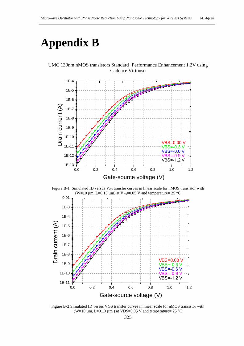
Microwave Oscillator with Phase Noise Reduction Using Nanoscale Technology for Wireless Systems M. Aqeeli
325
Appendix B
UMC 130nm nMOS transistors Standard Performance Enhancement 1.2V using
Cadence Virtouso
0.0 0.2 0.4 0.6 0.8 1.0 1.2
1E-13
1E-12
1E-11
1E-10
1E-9
1E-8
1E-7
1E-6
1E-5
1E-4
Dra
in c
urr
en
t (A
)
Gate-source voltage (V)
Figure B-1 Simulated ID versus VGS transfer curves in linear scale for nMOS transistor with
(W=10 µm, L=0.13 µm) at VDS=0.05 V and temperature= 25 °C
0.0 0.2 0.4 0.6 0.8 1.0 1.2
1E-11
1E-10
1E-9
1E-8
1E-7
1E-6
1E-5
1E-4
1E-3
0.01
Dra
in c
urr
en
t (A
)
Gate-source voltage (V)
Figure B-2 Simulated ID versus VGS transfer curves in linear scale for nMOS transistor with
(W=10 µm, L=0.13 µm ) at VDS=0.05 V and temperature= 25 °C

Microwave Oscillator with Phase Noise Reduction Using Nanoscale Technology for Wireless Systems M. Aqeeli
326
0.0 0.2 0.4 0.6 0.8 1.0 1.2
1.0x10⁻³
2.0x10⁻³
3.0x10⁻³
4.0x10⁻³
5.0x10⁻³
6.0x10⁻³
7.0x10⁻³
Dra
in c
urr
en
t (A
)
Gate-source voltage (V)Figure B-3 Simulated ID versus VGS transfer curves in linear scale for nMOS transistor with
(W=10 µm, L=0.13 µm ) at VDS=1.2 V and temperature= 25 °C
0.0 0.2 0.4 0.6 0.8 1.0 1.2
2.0x10⁻⁵
4.0x10⁻⁵
6.0x10⁻⁵
8.0x10⁻⁵
1.0x10⁻⁴
1.2x10⁻⁴
1.4x10⁻⁴
Dra
in c
urr
en
t (A
)
Gate-source voltage (V)
Figure B-4 Simulated ID versus VGS transfer curves in linear scale for nMOS transistor with
(W=0.16 µm, L=0.13 µm ) at VDS=1.2 V and temperature= 25 °C
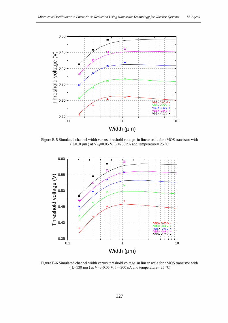
Microwave Oscillator with Phase Noise Reduction Using Nanoscale Technology for Wireless Systems M. Aqeeli
327
0.1 1 10
0.25
0.30
0.35
0.40
0.45
0.50
Thre
sho
ld v
olta
ge
(V
)
Width (m)
Figure B-5 Simulated channel width versus threshold voltage in linear scale for nMOS transistor with
( L=10 µm ) at VDS=0.05 V, ID=200 nA and temperature= 25 °C
0.1 1 10
0.35
0.40
0.45
0.50
0.55
0.60
Th
resh
old
vo
lta
ge
(V
)
Width (m)
Figure B-6 Simulated channel width versus threshold voltage in linear scale for nMOS transistor with
( L=130 nm ) at VDS=0.05 V, ID=200 nA and temperature= 25 °C

Microwave Oscillator with Phase Noise Reduction Using Nanoscale Technology for Wireless Systems M. Aqeeli
328
0.0 0.2 0.4 0.6 0.8 1.0 1.2
1.20x10⁻³
2.40x10⁻³
3.60x10⁻³
4.80x10⁻³
6.00x10⁻³
7.20x10⁻³
8.40x10⁻³
Tra
nscon
du
cta
nce (
A/V
)
Gate-source voltage (V)
Figure B-7 Simulated transfer conductance curves versus VGS in linear scale for nMOS transistor with for
nMOS transistor with (W=10 µm, L= 0.13 µm) at VDS=1.2 V and temperature= 25 °C
0.0 0.2 0.4 0.6 0.8 1.0 1.2
2.10x10⁻⁵
4.20x10⁻⁵
6.30x10⁻⁵
8.40x10⁻⁵
1.05x10⁻⁴
1.26x10⁻⁴
1.47x10⁻⁴
Tra
nscon
du
cta
nce (
A/V
)
Gate-source voltage (V)
Figure B-8 Simulated transfer conductance curves versus VGS in linear scale for nMOS transistor with for
nMOS transistor with (W=10 µm, L=0.13 µm) at VDS=1.2 V and temperature= 25 °C

Microwave Oscillator with Phase Noise Reduction Using Nanoscale Technology for Wireless Systems M. Aqeeli
329
Appendix C
C1 C2
C1C2
C1 C2
C1C2
C1 C2
C1C2
C1 C2
C1C2
C1 C2
C1C2C1 C2
1X
2X
8X
Figure C-1 Top view of Mesh MOM capacitor
M1
M2
M3
M4
M5
M6
Figure C-2 Cross view of Mesh MOM capacitor

Microwave Oscillator with Phase Noise Reduction Using Nanoscale Technology for Wireless Systems M. Aqeeli
330
Appendix D
VCO gain and tuning frequency versus capacitance for various control voltages.
clc
close all
clear all
Cs = 10*10^-14;
n = 4;
L =300*10^-10;
Cb =(10:2:100).*1e-15;
Q = 1.6*(10.^-19);
V =.2:0.2:.8;
mu =
['o','s','d','*','<','.','>',':','o','.','*','o','s','d','*
','<','.','>',':','o','.','*'];
for ii=1:length(V)
Delta_Q(ii) = Q/(V(ii)^2);
Cv(ii) = Q/V(ii);
Gain=[];Freq = [];
for i=1:length(Cb)
Gain(i) = ((1/(2*pi))*(((Cs^2)*L)/((((Cs +
Cv(ii))^2)*((L*(Cb(i) + ((2*Cs*Cv(ii))/(Cs + Cv(ii))) +
(n*Cv(ii))))^(3/2))))))*Delta_Q(ii) ;
Ct(i) = (2*Cs*Cv(ii)/(Cs + Cv(ii))) + (n*Cv(ii)) + Cb(i);
Freq(i) = 1./(2*pi*sqrt(L*Ct(i)));
end

Microwave Oscillator with Phase Noise Reduction Using Nanoscale Technology for Wireless Systems M. Aqeeli
331
Gain_tot(ii,:) = Gain;
FreqT(ii,:) =Freq;
figure(D-1)
hold on
plot(Cb./1e-15,Gain_tot(ii,:)./1e6,'ks-')
grid on
xlabel('Cb (fF)')
ylabel('Kvco (MHz/V)')
figure(D-2)
hold on
a_test = [' t=' , num2str(V(ii)) ,' um '];
a_legend(ii,1:length(a_test)) = a_test;
plot(Cb./1e-15,FreqT(ii,:)./1e9,'bo-')
grid on
hold on
xlabel('Cb (fF)')
ylabel('Frequency (GHz)')
legend('V = 0.2 V')
figure(3)
hold on
plot(Cb./1e-15,Gain_tot(ii,:)./1e6,mu(ii))
grid on
hold on
xlabel('Cb (fF)')
ylabel('Kvco (MHz/V)')
end
% % % % % S4(i) = Delta_Q(ii)*((((Cs^2) + ((Cs +
Cv)^2)*n)*(T(i)^(3/2)))/(4*sqrt(Cs +
Cv)*sqrt(L)*(pi)*((Cs*(Cs + Cv) + Cv*(Cs + (Cs +
Cv)*n)*T(i))^(3/2))));

Microwave Oscillator with Phase Noise Reduction Using Nanoscale Technology for Wireless Systems M. Aqeeli
332
FreqT
%
% figure(D-3)
% hold on
% plot(T,F_tot,'ks-')
% % grid on
% figure(D-4)
% hold on
% plot(T,F_tot(6:8,:),'ks-')
% grid on
% xlabel('T')
% ylabel('VCO Gain')
% figure(D-5)
% hold on
% plot(T,F_tot(11:15,:),'ks-')
% grid on
% xlabel('T')
% ylabel('VCO Gain')

Microwave Oscillator with Phase Noise Reduction Using Nanoscale Technology for Wireless Systems M. Aqeeli
333
Figure D-1 VCO gain and digital switching varactor bank as the functions of control voltage
Figure D-2 VCO oscillation frequency and digital switching varactor bank at 0.2V
10 20 30 40 50 60 70 80 90 1000
5
10
15
20
25
30
35
40
Cb (fF)
Kvco (
MH
z/V
)
V = 0.2 V
V = 0.4 V
V = 0.6 V
V = 0.8 V
10 20 30 40 50 60 70 80 90 1002
3
4
5
6
7
8
9
10
Cb (fF)
Fre
quency (
GH
z)
V = 0.2 V