microwave network analysis -...
TRANSCRIPT


2
Text Book
• D.M. Pozar, “Microwave engineering”, 3rd edition, 2005 by John-Wiley & Sons.
• Fawwaz T. ILABY, “Fundamentals of Applied Electromagnetics”, 5th edition, 2007 by Prentice Hall
• M. N. Sadiku, Elements of Electromagnetics

Typical GSM Mobile Handset
3

4
Typical GSM Mobile Handset Cont...
• RF Front End consists of microwave circuits and components.
• High frequency or microwave circuit design techniques are used.
• Different from conventional low frequency circuit theories.
• Understanding of electromagnetism is crucial.
5
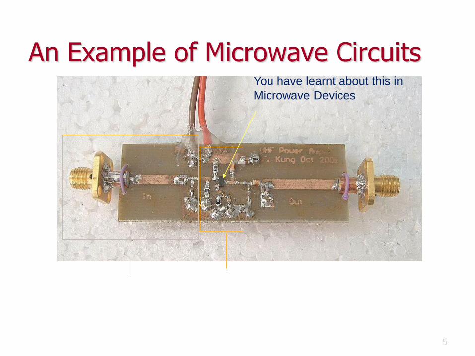
An Example of Microwave Circuits
This part will be covered in
RF transistor circuit design This is the
coverage of
Microwave components
& Circuits.
You have learnt about this in
Microwave Devices
6
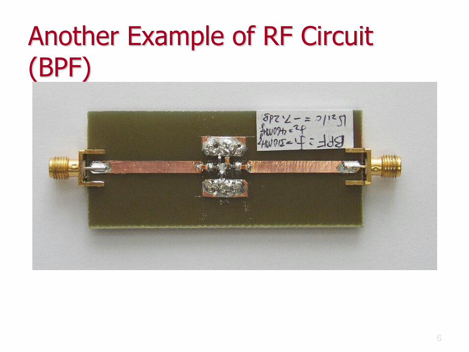
Another Example of RF Circuit (BPF)
7
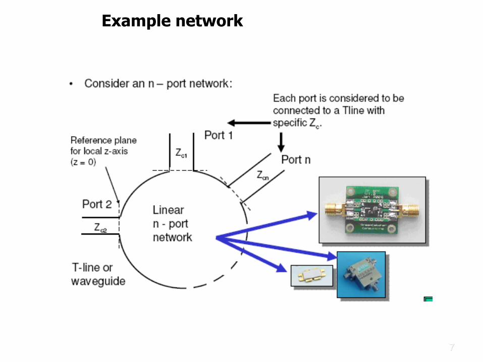
Example network

8
Microwave Circuit Cont...
Transmission Line

9
More Microwave/RF Components and Circuit Examples
• Integrated circuits:
Www.eecs.umich.edu/dp_groupMMIC
Www.signal.uu.se/research/microwave_technology/

10
Examples Cont...
• Discretes:
Www.elcon_inc.com/components.html
Www.shfmicro.com
Www.sphere.bc.ca/test/rf-semis..hmtl

11
Examples Cont... • Connectors, coaxial & waveguides:
Www.micckts.com Www.radiall.com/products/focus/idx2.htm
Www.mcecompanies.com/weinschel.hmt
12
Examples Cont...
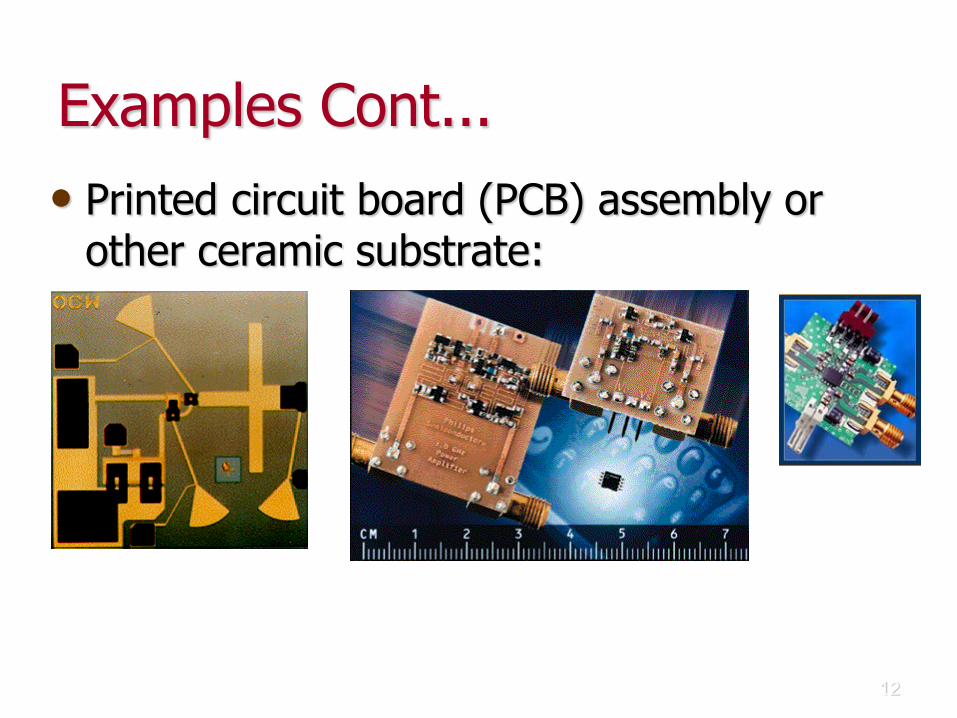
• Printed circuit board (PCB) assembly or other ceramic substrate:
Www.eecs.umich.edu/dp_group/MMIC Www.semiconductors.philips.com
13
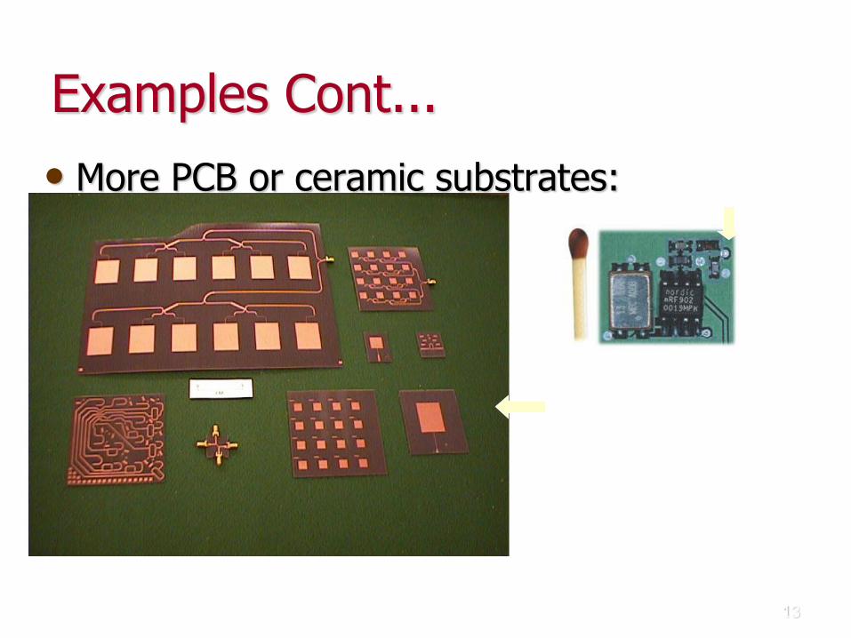
Examples Cont...
• More PCB or ceramic substrates:
Www.eng.ox.ax.uk/~comwww/radar.hmt
Microstrip antenna
Oscillator
14
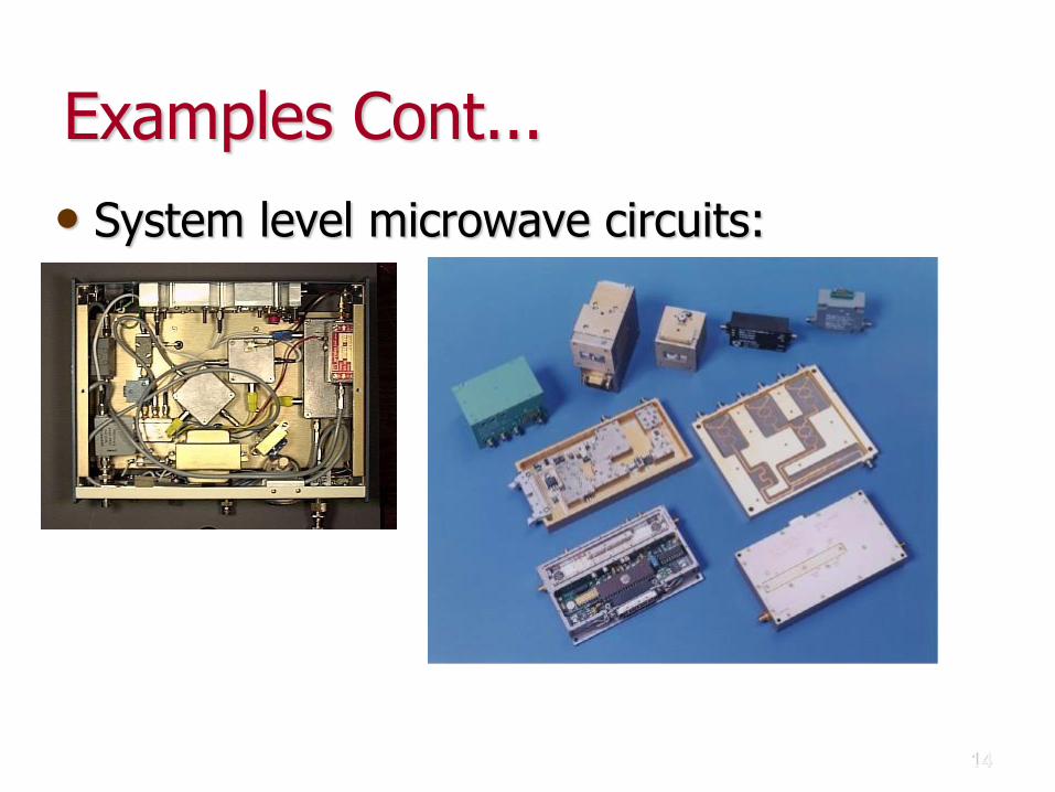
Examples Cont...
• System level microwave circuits:
Www.qsl.net/kesfx/tr503.html
Www.filss.com/components/content_products.html
15
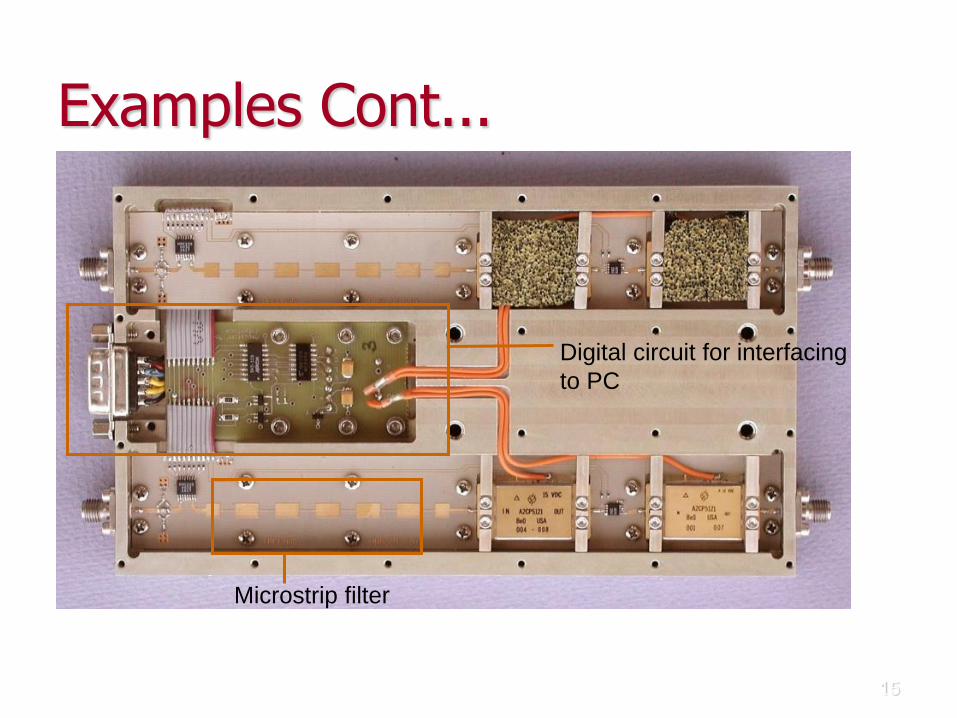
Examples Cont...
Dual band amplifier module, www.astro.umd.edu/~harris/instrumentation.html
Microstrip filter
Digital circuit for interfacing
to PC

16
Examples Cont...
Ivan board, www-personal.ksu.edu/~wkuhn/facil.html

INTRODUCTION • A microwave network is formed when a number of
microwave components and devices (e.g. oscillator, amplifier etc) is connected together by a TL or waveguide for microwave transmission.
• The point connecting the two or more devices is called the junction.
• For a low frequency network, a base is a pair of terminals. For a microwave network, a base is a reference plate which crosses the length of a TL or Waveguide.

• At a low frequency, the network physical length is very small compared to the of the signal sent. Thus, the measurable variable is the voltage and current at any points in the circuit.
• The phase change from one point to another is negligible.
• More interested to the voltage and current at one set of base, the power flow through a more global device or quantity.
• Can be related in term as Z-parameter, Y-parameter, h-parameter, or ABCD parameter.

• For a 2-base network, the relation is given by:
• Where Zij, Yij, h and A,B,C,D are suitable constants which characterises the junction.
2
2
1
1
2
1
2221
1211
2
1
2
1
2221
1211
2
1
2
1
2221
1211
2
1
D-
B
h
Y
Z
I
V
C
A
I
V
V
I
h
hh
I
V
V
V
Y
YY
I
I
I
I
Z
ZZ
V
V
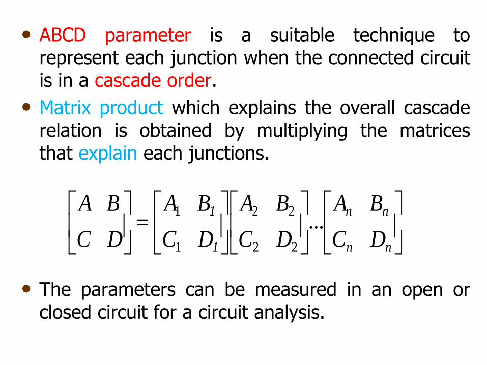
• ABCD parameter is a suitable technique to represent each junction when the connected circuit is in a cascade order.
• Matrix product which explains the overall cascade relation is obtained by multiplying the matrices that explain each junctions.
• The parameters can be measured in an open or closed circuit for a circuit analysis.
nn
nn
1
1
D C
B A
D C
B A
D C
B A
D C
B A...
22
22
1
1

• At a microwave frequency, the physical length of the component can be compared or longer than the wavelength. The voltage and current cannot be defined well at a given point on the microwave circuit.
• The measurement for Z, Y, h and ABCD parameters is difficult at this frequency because of the following reasons:
– There is no voltage and current terminal measuring device
– A closed and open circuit is difficult to obtain for a great frequency range.
– The presence of an active device causes the circuit to be instabilised for an open or closed circuit.

• Thus, a microwave circuit is usually analysed using a scatter parameter or S-parameter.
• It relates the reflection wave amplitude and the incident wave linearly.
• The S-parameter can be related to Z, Y or ABCD-parameters.

23
Example of Terminations
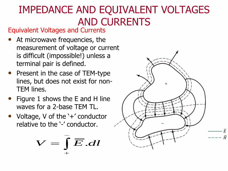
IMPEDANCE AND EQUIVALENT VOLTAGES AND CURRENTS
Equivalent Voltages and Currents
• At microwave frequencies, the measurement of voltage or current is difficult (impossible!) unless a terminal pair is defined.
• Present in the case of TEM-type lines, but does not exist for non-TEM lines.
• Figure 1 shows the E and H line waves for a 2-base TEM TL.
• Voltage, V of the ‘+’ conductor relative to the ‘-’ conductor.
dlEV .

• The current flowing on the ‘+’ conductor can be determined using Ampere’s Law.
• Characteristic impedance Zo for traveling waves
• We may use the circuit theory for TL to characterise this line as a circuit element.
• For a non-TEM, it is more difficult to obtain this parameter => use the equivalent concept.
c
dlHI .
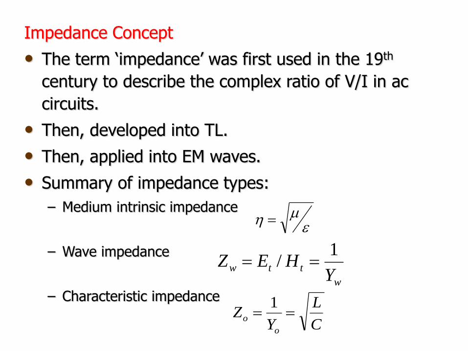
Impedance Concept
• The term ‘impedance’ was first used in the 19th
century to describe the complex ratio of V/I in ac
circuits.
• Then, developed into TL.
• Then, applied into EM waves.
• Summary of impedance types:
– Medium intrinsic impedance
– Wave impedance
– Characteristic impedance
w
ttwY
HEZ1
/
C
L
YZ
o
o 1

IMPEDANCE & ADMITTANCE MATRICES
• Equivalent currents & voltages can be defined for TEM & non-TEM waves.
• Once they have been defined at various points in the microwave network, the impedance & admittance matrix can be used to relate these port quantities.
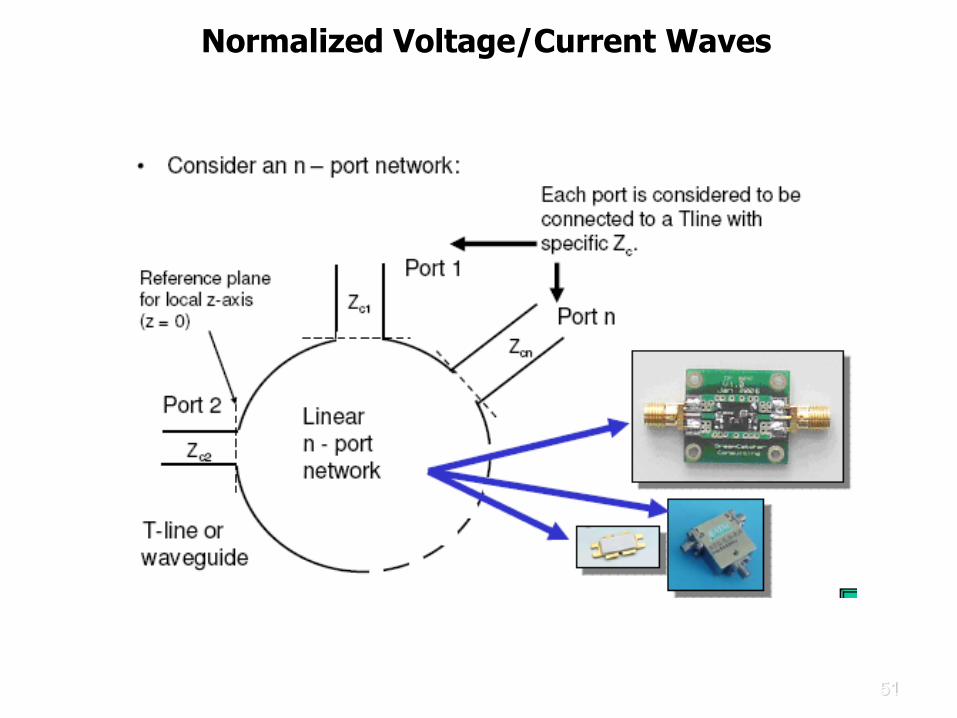
• Consider N-port or arbitrary N-port microwave network (Figure 2).
• The port in Figure 2 can be any TL or one of the propagating modes in waveguides.

• A base refers to a pair of 2-terminals.
• If one of the network base is a waveguide supporting more than one propagating modes, additional electric base is required for every mode.
• At a given point at the nth base, terminal plate, tn, is defined together with the equivalent voltage and current for the incident and reflection wave (Vn
+, In+ and Vn
-, In-).
• The terminal planes are important in providing a phase reference for voltage and current phasors.

Figure 2

• At the nth terminal plate, the total voltage and current is given by:
• The impedance matrix [Z] for a microwave network relating this voltage and current is :

• Or in matrix form as
• Admittance matrix [Y]:
• Or in matrix form as
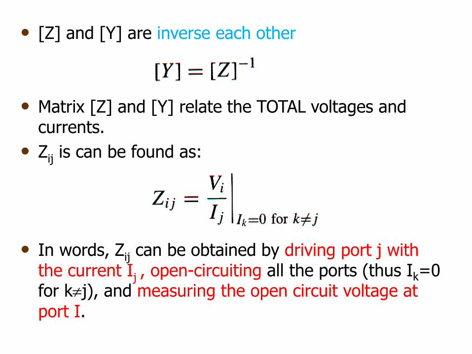
• [Z] and [Y] are inverse each other
• Matrix [Z] and [Y] relate the TOTAL voltages and currents.
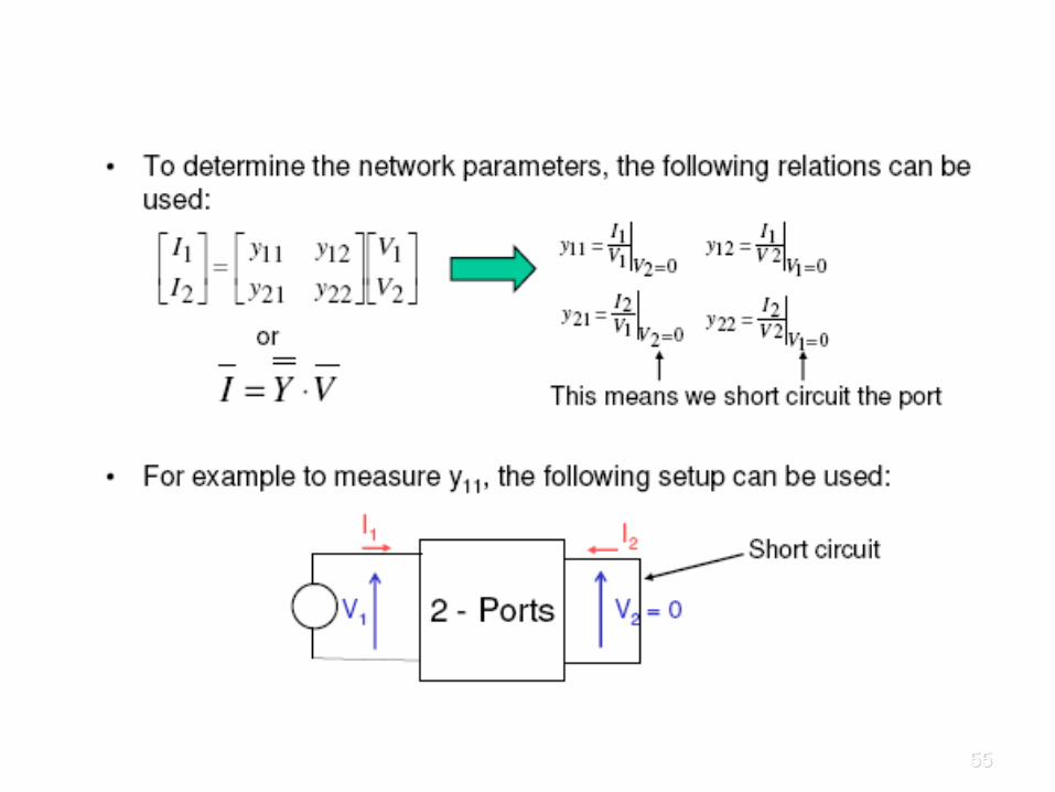
• Zij is can be found as:
• In words, Zij can be obtained by driving port j with the current Ij , open-circuiting all the ports (thus Ik=0 for kj), and measuring the open circuit voltage at port I.
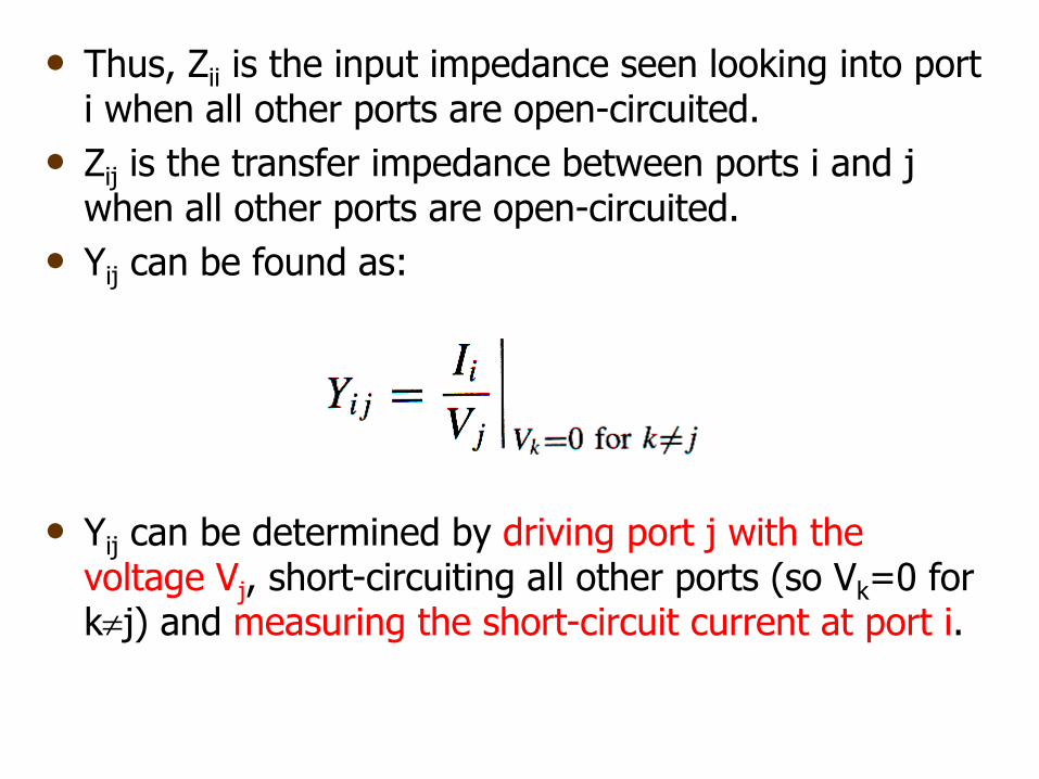
• Thus, Zii is the input impedance seen looking into port i when all other ports are open-circuited.
• Zij is the transfer impedance between ports i and j when all other ports are open-circuited.
• Yij can be found as:
• Yij can be determined by driving port j with the voltage Vj, short-circuiting all other ports (so Vk=0 for kj) and measuring the short-circuit current at port i.
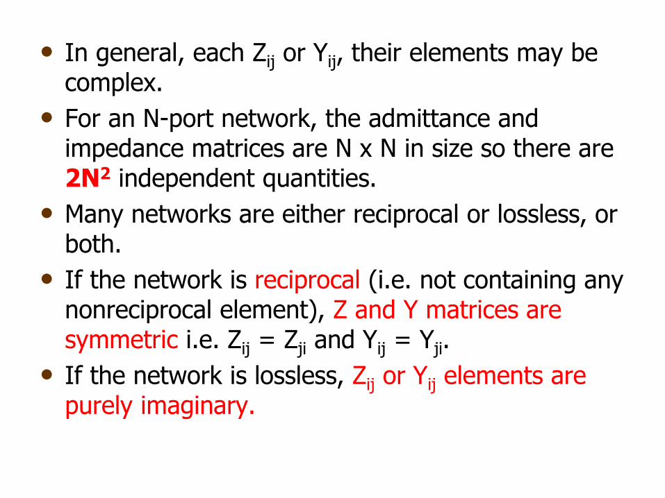
• In general, each Zij or Yij, their elements may be complex.
• For an N-port network, the admittance and impedance matrices are N x N in size so there are 2N2 independent quantities.
• Many networks are either reciprocal or lossless, or both.
• If the network is reciprocal (i.e. not containing any nonreciprocal element), Z and Y matrices are symmetric i.e. Zij = Zji and Yij = Yji.
• If the network is lossless, Zij or Yij elements are purely imaginary.
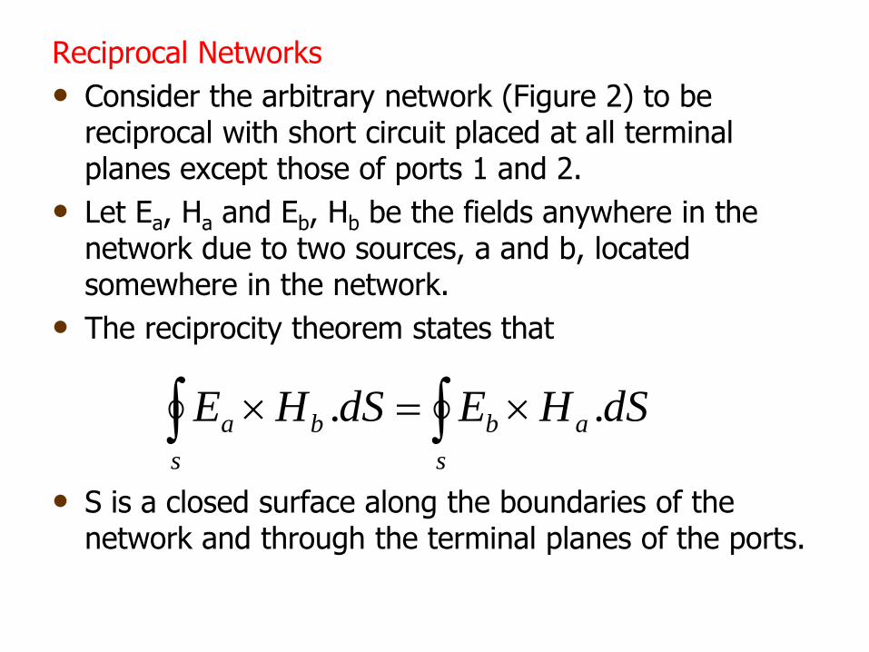
Reciprocal Networks
• Consider the arbitrary network (Figure 2) to be reciprocal with short circuit placed at all terminal planes except those of ports 1 and 2.
• Let Ea, Ha and Eb, Hb be the fields anywhere in the network due to two sources, a and b, located somewhere in the network.
• The reciprocity theorem states that
• S is a closed surface along the boundaries of the network and through the terminal planes of the ports.
dSHEdSHE a
s
bb
s
a ..

• If the boundary walls are metal, then Etan=0 on these walls.
• If they are open structures, the boundary can be taken far from the lines, so that Etan is negligible (nonzero).
• The nonzero quantity come from the cross-sectional areas of port 1 and 2.
• The fields due to sources a and b, evaluated from planes t1 and t2 are:
2222
2222
1111
1111
hIeV
hIeV
hIeV
hIeV
bb
aa
bb
aa
2b2b
2a2a
1b1b
1a1a
HE
HE
HE
HE

• e1, h1, e2 and h2 are the transverse modal fields of ports 1 and 2.
• Vs and Is are the equivalent voltages and currents.
• S1 and S2 are the cross-sectional areas at the terminal planes of ports 1 and 2.
• Thus,
V1aI1b – V1bI1a + V2aI2b – V2bI2a = 0
• Use the 2x2 admittance matrix of the 2-ports networks to eliminate the Is. So:
I1 = Y11V1 + Y12V2
I2 = Y21V1 + Y22V2

• Substitute into the previous equation:
(V1aI1b – V1bI1a)(Y12 – Y21) = 0
• V1a, V1b, V2a and V2b can take on arbitrary values. In
order to satisfy the above equation, Y12= Y21
Thus: Yij = Yji
• If [Y] is a symmetric matrix, then [Z] is also
symmetric.
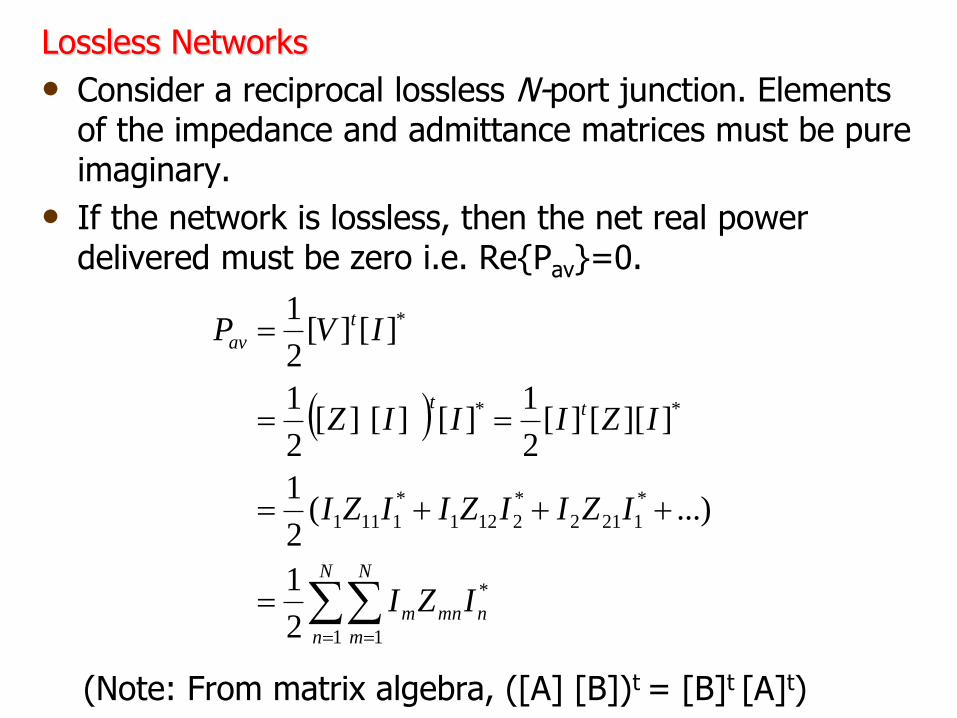
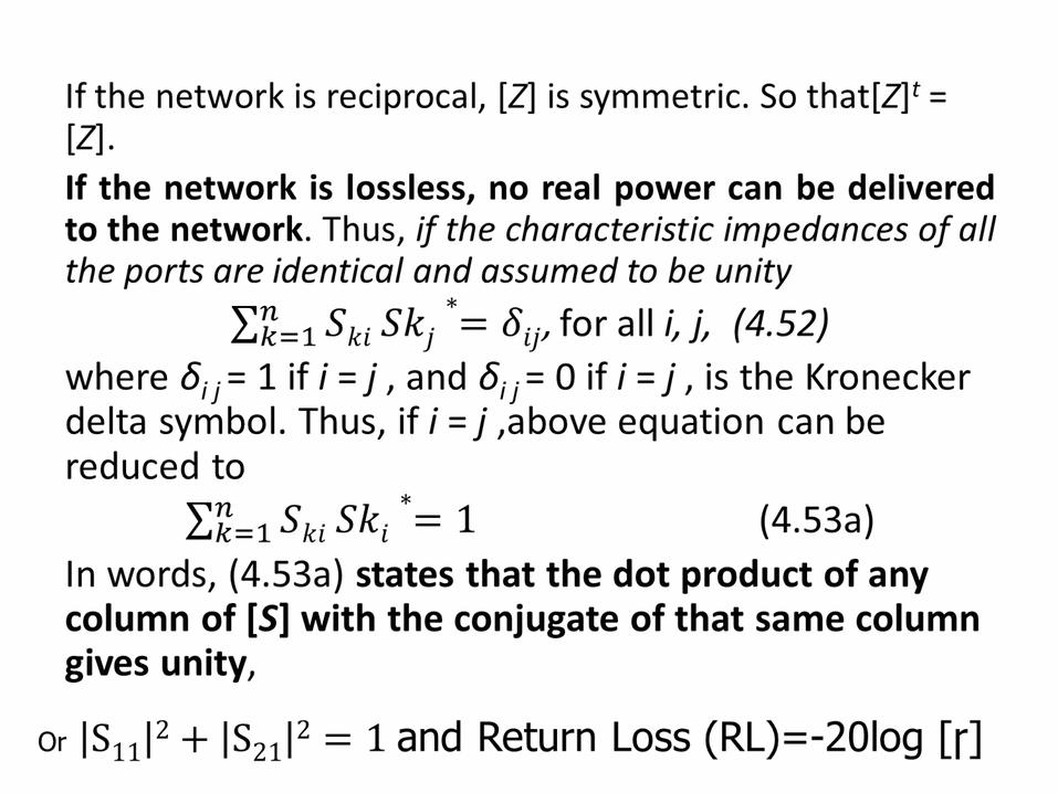
Lossless Networks
• Consider a reciprocal lossless N-port junction. Elements of the impedance and admittance matrices must be pure imaginary.
• If the network is lossless, then the net real power delivered must be zero i.e. Re{Pav}=0.
(Note: From matrix algebra, ([A] [B])t = [B]t [A]t)
*
1 1
*
1212
*
2121
*
1111
**
*
2
1
...)(2
1
]][[][2
1][][][
2
1
][][2
1
nmn
N
n
N
m
m
tt
t
av
IZI
IZIIZIIZI
IZIIIZ
IVP

• In current are independent, the self part of each self term InZnnIn
* are equal to zero since we could set all ports to zero except for the nth port.
• So,
ReInZnnIn* = |In|
2 Re {Znn} = 0
Or Re {Znn} = 0 because In 0
• Now let all port currents be zero except for Im and In.
Re {(InIm* + ImIn
*)Zmn} = 0
and Zmn = Znm
• But (InIm* + ImIn
*) is a purely real quantity (non-zero).
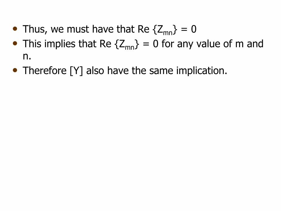
• Thus, we must have that Re {Zmn} = 0
• This implies that Re {Zmn} = 0 for any value of m and n.
• Therefore [Y] also have the same implication.

EXERCISE

Answer
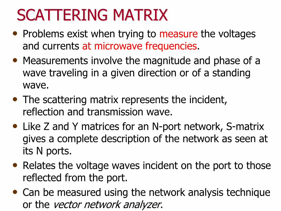
SCATTERING MATRIX • Problems exist when trying to measure the voltages
and currents at microwave frequencies.
• Measurements involve the magnitude and phase of a wave traveling in a given direction or of a standing wave.
• The scattering matrix represents the incident, reflection and transmission wave.
• Like Z and Y matrices for an N-port network, S-matrix gives a complete description of the network as seen at its N ports.
• Relates the voltage waves incident on the port to those reflected from the port.
• Can be measured using the network analysis technique or the vector network analyzer.

Network Analyzer

46
Practical Measurement of S -parameters

47
S/Scattering Parameters
•If the n – port network is linear there is a linear
relationship between the normalized waves. •For instance if we energize port 2:

48
S-Parameters - Why Do We Need Them
•Usually we use Y, Z, H or ABCD parameters to describe a
linear two port network. •These parameters require us to open or short a network to
find the parameters. •At radio frequencies it is difficult to have a proper short or
open circuit, there are parasitic inductance and capacitance in
most instances. •Open and short conditions lead to standing wave, which can
cause oscillation and destruction of the device.
•For non-TEM propagation mode, it is not possible to measure
voltage and current. We can only measure power from E and
H fields

49
• Hence a new set of parameters (S) is
needed which
•Do not need open/short condition. •Do not cause standing wave. •Relates to incident and reflected power
waves, instead of voltage and current.

50
S-parameters
• As oppose to V and I, S-parameters relate the reflected and
incident voltage waves.
• S-parameters have the following advantages:
•Relates to familiar measurement such as reflection coefficient, gain, loss etc.
•Can cascade S-parameters of multiple devices to predict
system performance (similar to ABCD parameters).
•Can compute Z, Y or H parameters from S-parameters if
needed.
51
Normalized Voltage/Current Waves

52
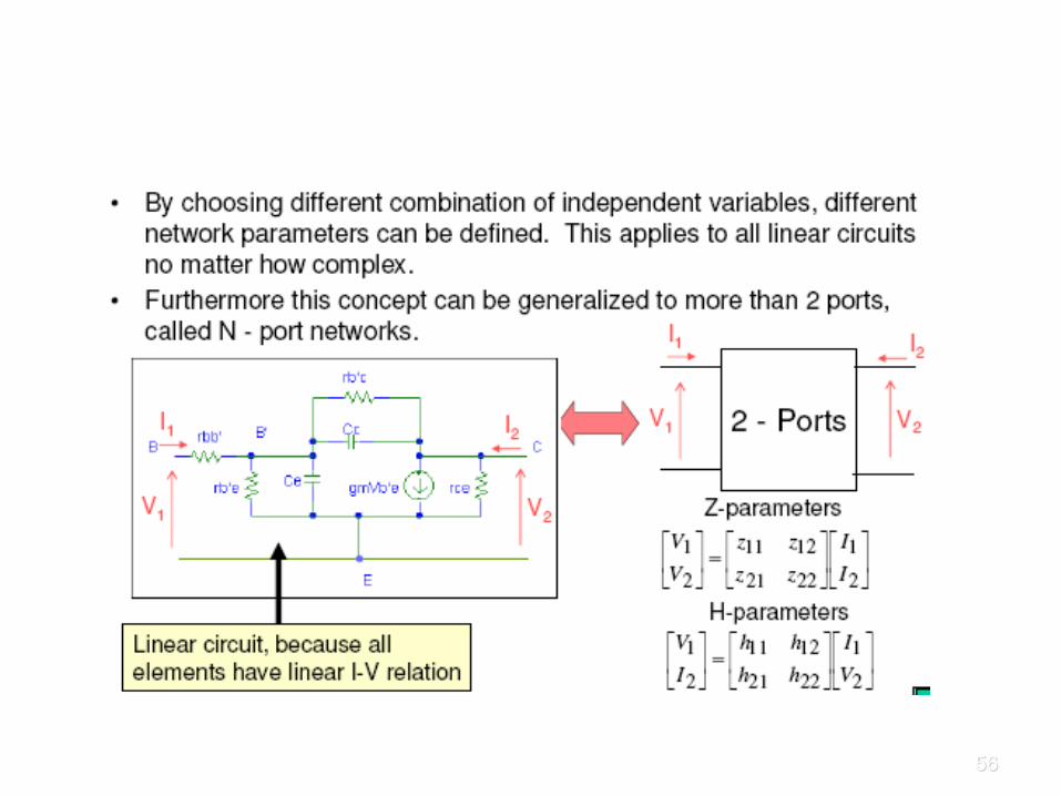
Network Parameters
•Many times we are only interested in the voltage (V)
and current (I) relationship at the terminals/ports of a
complex circuit. •If mathematical relations can be derived for V and I,
the circuit can be considered as a black box. •For a linear circuit, the I-V relationship is linear and
can be written in the form of matrix equations. •A simple example of linear 2-port circuit is shown
below. Each port is associated with 2 parameters,
the V and I.

53

54
55
56

• After the scattering parameter is unknown, the change into other matrix parameter can be done.
• Consider an N-port network (Figure 2), Vn+ is the
amplitude of the voltage wave incident on port n and Vn
- is the amplitude of the voltage wave reflected from port n.
• The scattering matrix [S] is defined as:
nn V
V
VS
V
V
V
.
.
.
S . . . S
.
. .
. .
. S
S . . . S
.
.
.
2
1
NNN1
21
1N1211
2
1
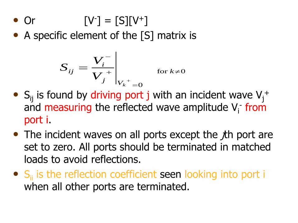
• Or [V-] = [S][V+]
• A specific element of the [S] matrix is
• Sij is found by driving port j with an incident wave Vj+
and measuring the reflected wave amplitude Vi- from
port i.
• The incident waves on all ports except the jth port are set to zero. All ports should be terminated in matched loads to avoid reflections.
• Sii is the reflection coefficient seen looking into port i when all other ports are terminated.
0for
0
k
Vj
iij
k
V
VS
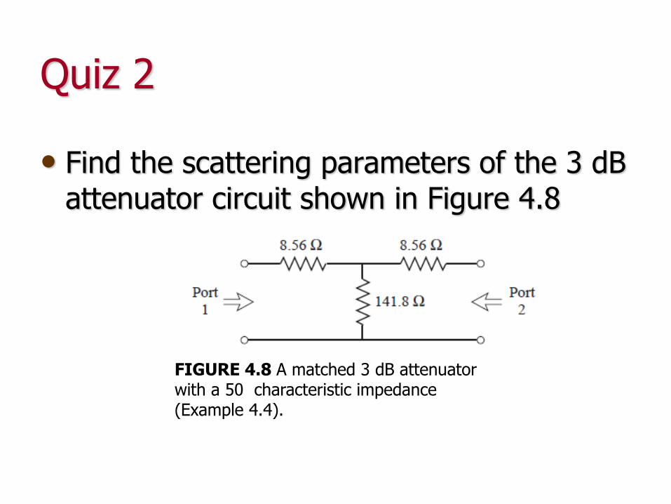
Quiz 2
• Find the scattering parameters of the 3 dB attenuator circuit shown in Figure 4.8
FIGURE 4.8 A matched 3 dB attenuator with a 50 characteristic impedance (Example 4.4).

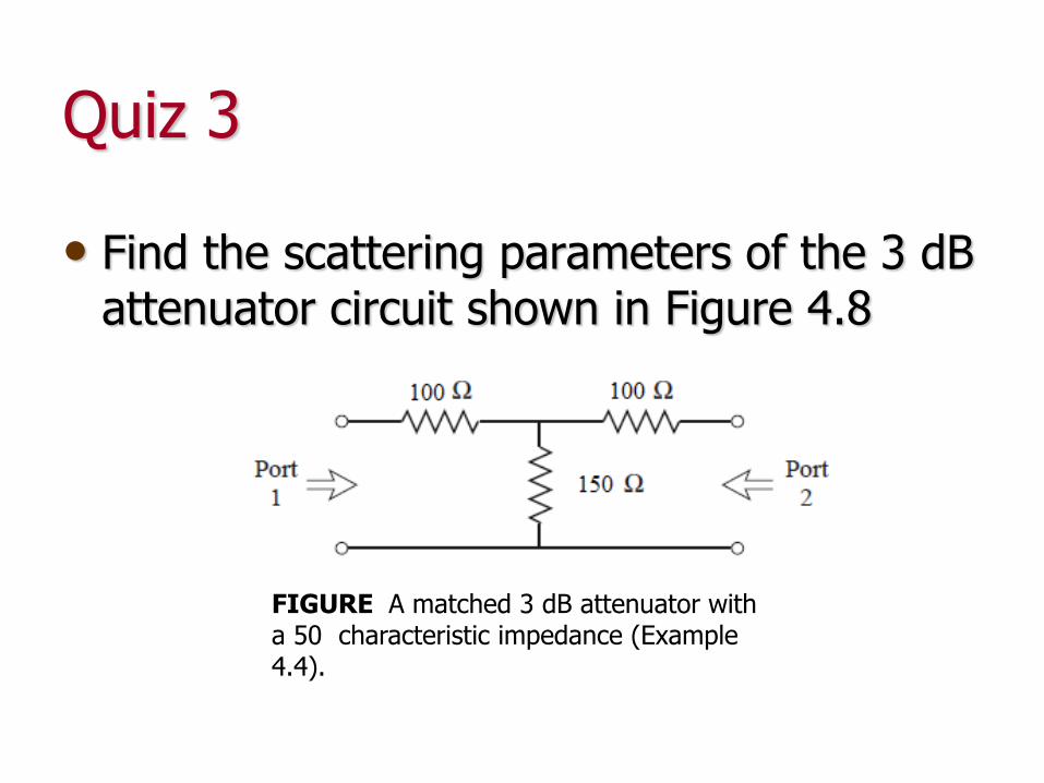
• Find the scattering parameters of the 3 dB attenuator circuit shown in Figure 4.8
FIGURE A matched 3 dB attenuator with a 50 characteristic impedance (Example 4.4).
Quiz 3

• We now show how the [S] matrix can be determined from the [Z] or [Y] matrices, or vice versa.
• First assumption, the characteristic impedance Zon for all ports are the same. For convenience, assume Zon = 1.
• The total voltage and current at the port can be written as
Vn = Vn+ + Vn
-
In = In+ - In
- = Vn+ - Vn
-
• Using the definition of [Z] is [V] = [Z] [I] gives:
• Rewritten as:
[Z][I] = [Z][V+] - [Z][V-] = [V] = [V+] + [V-]
([Z] + [u])[V-] = ([Z] - [u])[V+]

• Where [u] is the unit matrix:
• Therefore:
[S] = ([Z] + [u])-1([Z] – [u])
• Giving S matrix in terms of the impedance matrix.
1 . . . 0
. . .
. . .
. 1 0
0 . . . 0 1
][u

• For a one port network:
• To obtain [Z] in terms of [S];
[Z][S] + [u][S] = [Z] – [u]
• Giving:
[Z] = ([u] + [S])([u] – [S])-1
1
1
11
1111
Z
ZS
Reciprocal Networks and Lossless Networks
• The [S] matrix for reciprocal networks are symmetric. A lossless network is unitary (please refer to Pozar’s).
• The S-parameter shows that a reflection coefficient sees to an n-port as unequal to Snn, except if all other ports are a match.
• The transmission coefficient from an m-port to an n-port is not Snm, except if all other ports are a match.
• Changing the network termination or excitation will not change the S-parameter but may change the reflection or transmission coefficient.

• A two-port network is known to have the following scattering matrix:
• Determine - is the network reciprocal? -is the network lossless?. -If port 2 is terminated with a matched load, what is the return loss seen at port 1? -If port 2 is terminated with a short circuit, what is the return loss seen at port 1?
Quiz 4
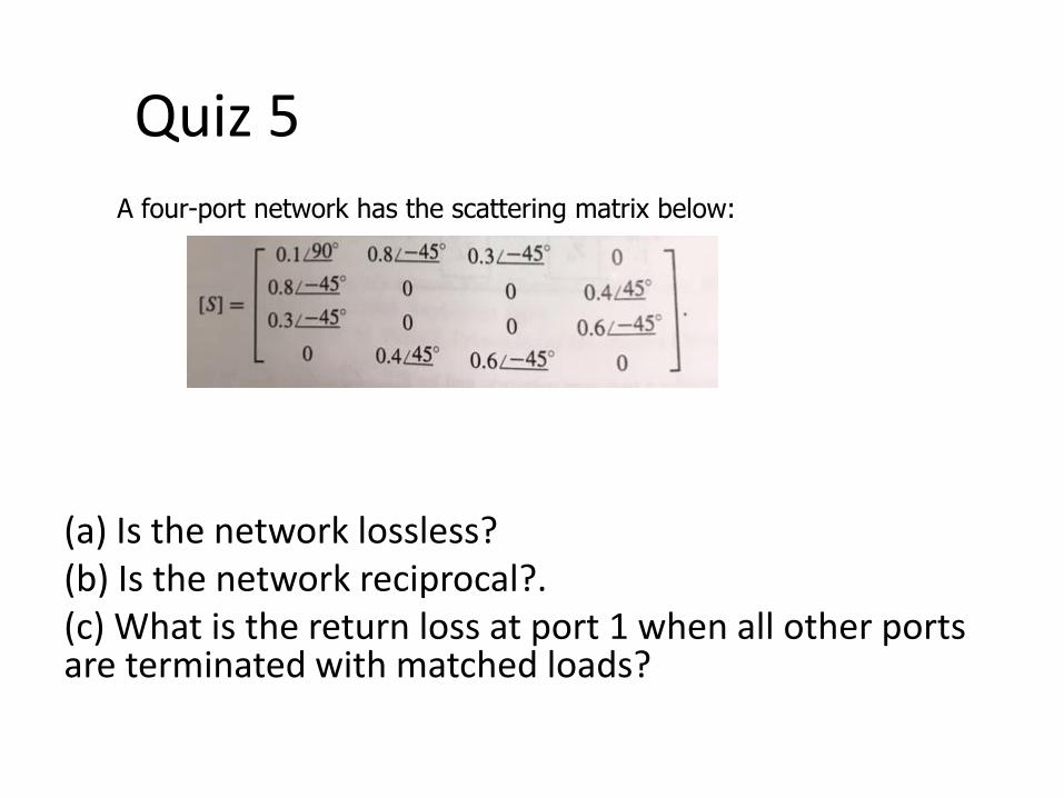
(a) Is the network lossless? (b) Is the network reciprocal?. (c) What is the return loss at port 1 when all other ports are terminated with matched loads?
Quiz 5
A four-port network has the scattering matrix below:

A Shift in Reference Planes
• Because the S-parameters relate the amplitudes of incident and reflection waves, so reference planes must be specified for each port.
• The S-parameter are transformed when the reference planes are removed from the original planes.
• Consider this network:
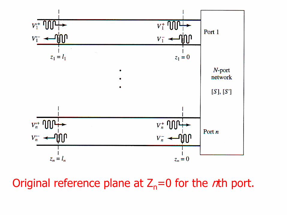
Original reference plane at Zn=0 for the nth port.

• The S-parameter for this network is called [S].
• Consider a new set with a reference plane Zn=ln.
• The new S-parameter is named [S’].
• In terms of the incident and reflected voltage:
• From the theory of wave propagation, we can relate the new wave to the original one
• Wheren=nln is the electrical length of the shift of the reference plane.
*

• In matrix form:
• Multply with the inverse matrix on the left gives:
• Compare with*
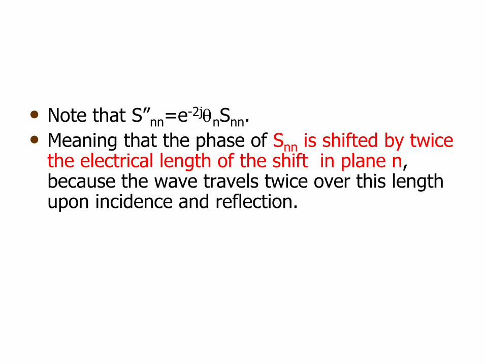
• Note that S”nn=e-2jnSnn.
• Meaning that the phase of Snn is shifted by twice the electrical length of the shift in plane n, because the wave travels twice over this length upon incidence and reflection.

74
ABCD Parameters
Of particular interest in RF and microwave systems is ABCD parameters. ABCD parameters are the most useful for representing transmission line and other linear microwave components in general.

75
• The ABCD matrix is useful for characterizing the overall
response of 2-port networks that are cascaded to each other.

76
THANK YOU