microprocessor lab manual
TRANSCRIPT
EC204-Microprocessor Lab
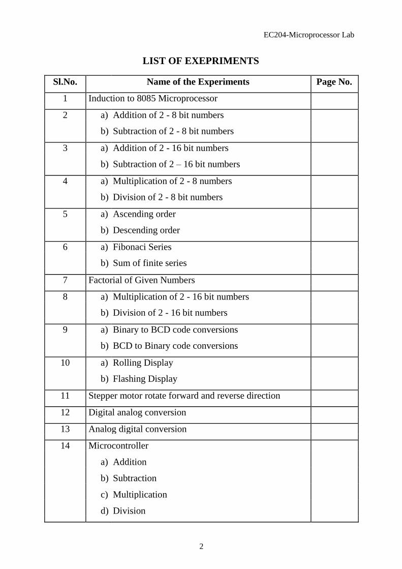
LIST OF EXEPRIMENTS
Sl.No. Name of the Experiments Page No.
1 Induction to 8085 Microprocessor
2 a) Addition of 2 - 8 bit numbers
b) Subtraction of 2 - 8 bit numbers
3 a) Addition of 2 - 16 bit numbers
b) Subtraction of 2 – 16 bit numbers
4 a) Multiplication of 2 - 8 numbers
b) Division of 2 - 8 bit numbers
5 a) Ascending order
b) Descending order
6 a) Fibonaci Series
b) Sum of finite series
7 Factorial of Given Numbers
8 a) Multiplication of 2 - 16 bit numbers
b) Division of 2 - 16 bit numbers
9 a) Binary to BCD code conversions
b) BCD to Binary code conversions
10 a) Rolling Display
b) Flashing Display
11 Stepper motor rotate forward and reverse direction
12 Digital analog conversion
13 Analog digital conversion
14 Microcontroller
a) Addition
b) Subtraction
c) Multiplication
d) Division
2
EC204-Microprocessor Lab
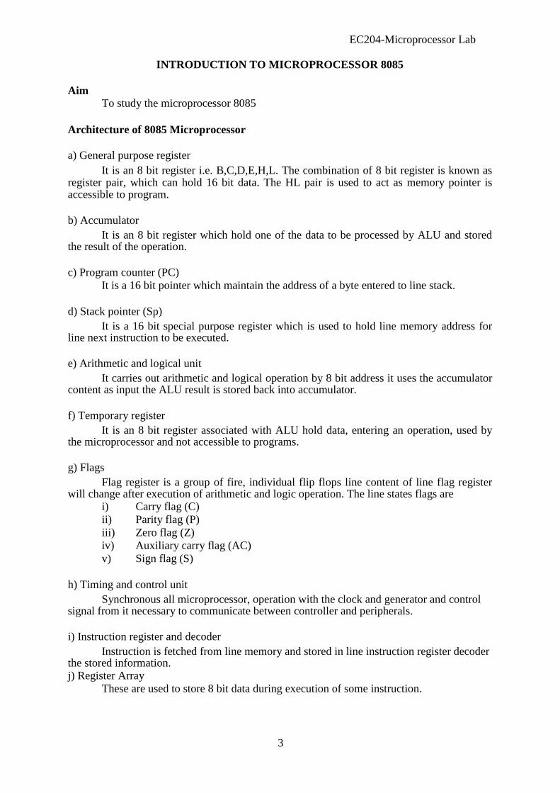
INTRODUCTION TO MICROPROCESSOR 8085
Aim To study the microprocessor 8085
Architecture of 8085 Microprocessor a) General purpose register
It is an 8 bit register i.e. B,C,D,E,H,L. The combination of 8 bit register is known as register pair, which can hold 16 bit data. The HL pair is used to act as memory pointer is accessible to program.
b) Accumulator It is an 8 bit register which hold one of the data to be processed by ALU and stored
the result of the operation.
c) Program counter (PC)
It is a 16 bit pointer which maintain the address of a byte entered to line stack.
d) Stack pointer (Sp)
It is a 16 bit special purpose register which is used to hold line memory address for line next instruction to be executed.
e) Arithmetic and logical unit It carries out arithmetic and logical operation by 8 bit address it uses the accumulator
content as input the ALU result is stored back into accumulator.
f) Temporary register It is an 8 bit register associated with ALU hold data, entering an operation, used by
the microprocessor and not accessible to programs.
g) Flags Flag register is a group of fire, individual flip flops line content of line flag register
will change after execution of arithmetic and logic operation. The line states flags are i) Carry flag (C)
ii) Parity flag (P)
iii) Zero flag (Z)
iv) Auxiliary carry flag (AC)
v) Sign flag (S)
h) Timing and control unit
Synchronous all microprocessor, operation with the clock and generator and control signal from it necessary to communicate between controller and peripherals.
i) Instruction register and decoder Instruction is fetched from line memory and stored in line instruction register decoder
the stored information. j) Register Array
These are used to store 8 bit data during execution of some instruction. 3
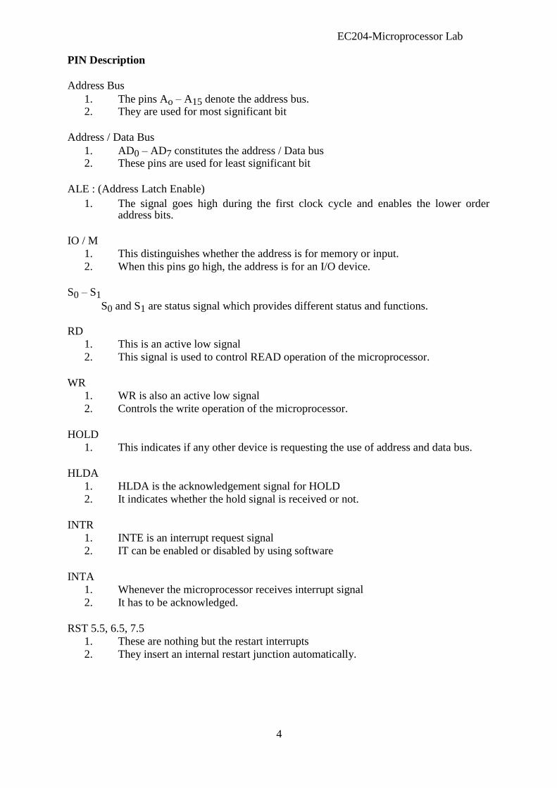
EC204-Microprocessor Lab PIN Description Address Bus
1. The pins Ao – A15 denote the address bus. 2. They are used for most significant bit
Address / Data Bus
1. AD0 – AD7 constitutes the address / Data bus 2. These pins are used for least significant bit
ALE : (Address Latch Enable) 1. The signal goes high during the first clock cycle and enables the lower order
address bits.
IO / M
1. This distinguishes whether the address is for memory or input.
2. When this pins go high, the address is for an I/O device.
S0 – S1
S0 and S1 are status signal which provides different status and functions. RD
1. This is an active low signal
2. This signal is used to control READ operation of the microprocessor.
WR
1. WR is also an active low signal
2. Controls the write operation of the microprocessor.
HOLD
1. This indicates if any other device is requesting the use of address and data bus.
HLDA
1. HLDA is the acknowledgement signal for HOLD
2. It indicates whether the hold signal is received or not.
INTR
1. INTE is an interrupt request signal
2. IT can be enabled or disabled by using software
INTA
1. Whenever the microprocessor receives interrupt signal
2. It has to be acknowledged.
RST 5.5, 6.5, 7.5
1. These are nothing but the restart interrupts
2. They insert an internal restart junction automatically. 4

EC204-Microprocessor Lab TRAP
1. Trap is the only non-maskable interrupt
2. It cannot be enabled (or) disabled using program.
RESET IN
1. This pin resets the program counter to 0 to 1 and results interrupt enable and HLDA flip flops.
X1, X2
These are the terminals which are connected to external oscillator to produce the necessary and suitable clock operation.
SID
This pin provides serial input data
SOD
This pin provides serial output data
VCC and VSS
1. VCC is +5V supply pin
2. VSS is ground pin Specifications
1. Processors
Intel 8085 at E144 MHz clock
2. Memory
Monitor RAM: 0000 – IFFF
EPROM Expansion: 2000 – 3FFF‟s
0000 – FFF
System RAM: 4000 – 5FFF
Monitor data area 4100 – 5FFF
RAM Expansion 6000 – BFFF
3. Input / Output Parallel: A8 TTL input timer with 2 number of 32-55 only input timer available in -85 EBI.
Serial: Only one number RS 232-C, Compatible, crucial interface using 8281A
Timer: 3 channel -16 bit programmable units, using 8253 channel „0‟ used for no band late. Clock generator. Channel „1‟ is used for single stopping used program.
Display: 6 digit – 7 segment LED display with filter 4 digit for adder display and 2 digit for data display.
Key board: 21 keys, soft keyboard including common keys and hexa decimal keys. RES: Reset keys allow to terminate any present activity and retain to - 85 its on initialize state.
5

EC204-Microprocessor Lab INT: Maskable interrupt connect to CPU‟s RST 7.5 interrupt
DEC: Decrement the adder by 1
EXEC: Execute line particular value after selecting address through go command.
NEXT: Increment the address by 1 and then display its content.
Key Functions:
E i. Hex entry key „0‟
ii. Substituting memory content where “next” key is paused immediately
0
after 1, take used to st cutting address.
SUB
iii. Register key „E‟
RD i) Hex code entry (1)
1 ii) Register key „D‟
REG
i) Hex code entry „2‟
C
ii) Retricre data from data „memory‟ to data top
2
iii) Register key „C‟
TN
B i) Hex code entry „3‟
3 ii) Retricre data from memory to top
TR iii) Register key „B‟
i) Hex key entry „C‟
F
4 ii) Block search from byte
BLOC iii) Register key „F‟
i) Hex key entry „5‟
A
ii) Fill block of RAM memory with desired data
5
iii) Register key „A‟
FILL
i) Hex key entry „6‟
L
ii) TN/Tl used for sending (or) receiving
6
iii) Register key „H‟
SER
H i) Hex key entry „7‟
7
ii) Register key „H‟
F2
6

I
8
G0
PL
9
SNG A
PH
F3
C
SH
MOV D
CMP B
SL
BC E
INS F
DEL
EC204-Microprocessor Lab i) Register key „S‟
ii) Register key „I‟ i) Hex key entry „A‟
ii) Function key F3 iii) Register key “ph”
i) Hex key entry “y”
ii) Signal step program (instruction by instruction) i) Hex key entry “c”
ii) Much a block of memory from a linear block
iii) Register key “SH”
i) Hex key D
ii) Compare 2 memory block i) Hex key entry „B‟
ii) Check a block from flame
iii) Register key “SPL”
i) Hex key „E‟
ii) Insert by test into memory (RAM)
i) Hex key „F‟
ii) Delete byte from memory RAM
System Power Consumption
Micro BSEB2 MICRO SSEB
+5V @ 1Amp +5V@ 800 mA
+12V @ 200 mA
- 12V @ 100 mA
7

EC204-Microprocessor Lab
Power Supply Specification
MICRO SSEM 230V, AC @ 80 Hz +5V @ 600 mA
Key Function
8

EC204-Microprocessor Lab IC‟s Used
8085 - 8 bit p
8253 - programmable internal timer 8255 - programmable peripheral interface
8279 - programmable key boards / display interface
8251 - programmable communication interface
2764 - 8 KV VV EPROM
6264 - 8K STATIC PROM
7414 - Hex inverter
7432 - Quad 21/p OR GATE
7409 - Quad 21/p AND GATE
7400 - NAND Gate
7404 - Dual D-FF
74373 - Octal „D‟ Latch
74139 - Dual 2 to 4 line decoder
74138 - 3 to 8 line decoder
9

EC204-Microprocessor Lab In Enter Program into Trainer Kit
1. Press „RESET‟ key
2. Sub (key processor represent address field)
3. Enter the address (16 bit) and digit in hex
4. Press „NEXT‟ key
5. Enter the data
6. Again press “NEXT” 7. Again after taking the program, are use HLT instruction
its Hex code 8. Press “NEXT”
How to executive program
1. Press “RESET”
2. Press “GO”
3. Enter the address location in which line program was executed
4. Press “Execute” key Result:
Thus 8085 microprocessor was studied successfully. 10
EC204-Microprocessor Lab
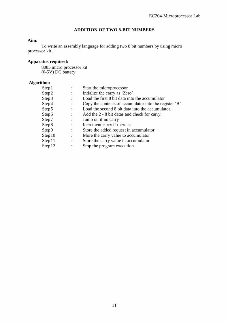
ADDITION OF TWO 8-BIT NUMBERS
Aim: To write an assembly language for adding two 8 bit numbers by using micro
processor kit.
Apparatus required: 8085 micro processor kit (0-5V) DC battery
Algorithm:
Step 1 : Start the microprocessor Step 2 : Intialize the carry as „Zero‟
Step 3 : Load the first 8 bit data into the accumulator
Step 4 : Copy the contents of accumulator into the register „B‟
Step 5 : Load the second 8 bit data into the accumulator.
Step 6 : Add the 2 - 8 bit datas and check for carry.
Step 7 : Jump on if no carry
Step 8 : Increment carry if there is
Step 9 : Store the added request in accumulator
Step 10 : More the carry value to accumulator
Step 11 : Store the carry value in accumulator
Step 12 : Stop the program execution. 11

EC204-Microprocessor Lab START
Intialise the carry as zero
Load the 1st
8 bit number
Transfer the 1st
number to register „B‟
Load the 2nd
8 bit number
Transfer and Add the contents of A and B
No Check for
carry? Yes
Increment carry by one
Store the added value in accumulator Move the contents of carry into accumulator
Store the value of carry in accumulator
END
12

EC204-Microprocessor Lab
Address Label Mnemonics Hex Code Comments
4100 MVI C,00 OE, 00 Initialize the carry as zero
4102 LDA 4300 3A, (00, 43) Load the first 8 bit data
4105 MOV, B,A 47 Copy the value of 8 bit data into register B
4106 LDA 4301 3A, (01, 43) Load the second 8 bit data into the accumulator
4109 ADD B 80 Add the hoo values
410A JNC D2, 0E, 41 Jump on if no carry
410D INR C OC If carry is there increment it
by one
410E Loop STA 4302 32 (02, 43) Stone the added value in the accumulator
4111 MOV A,C 79 More the value of carry to the accumulator from
register C
4112 STA 4303 32 (03, 43) Store the value of carry in the accumulator
4115 HLT 76 Stop the program execution
Input
Without carry
Input Address Value
4300 04
4301 02
Output
Output Address Value
4302 06
4303 00 (carry)
With carry
Input Address Value
4300 FF
4301 FF
Output Address Value
4302 FE
4303 01 (carry)
Calculation 1111 1111
1111 1111
---------------
(1) 1111 1110
=========
F E
Result: The assembly language program for 8 bit addition of two numbers was executed
successfully by using 8085 micro processing kit.
13

EC204-Microprocessor Lab
SUBTRACTION OF TWO 8 BIT NUMBERS
Aim: To write a assembly language program for subtracting 2 bit (8) numbers by using-
8085 micro processor kit.
Apparatus required: 8085 micro processor kit (0-5V) DC battery
Algorithm:
Step 1 : Start the microprocessor Step 2 : Intialize the carry as „Zero‟
Step 3 : Load the first 8 bit data into the accumulator
Step 4 : Copy the contents of contents into the register „B‟
Step 5 : Load the second 8 bit data into the accumulator.
Step 6 : Subtract the 2 8 bit datas and check for borrow.
Step 7 : Jump on if no borrow
Step 8 : Increment borrow if there is
Step 9 : 2‟s compliment of accumulator is found out
Step 10 : Store the result in the accumulator
Step 11 : More the borrow value from „c‟ to accumulator
Step 12 : Store the borrow value in the accumulator
Step 13 : Stop program execution
14

EC204-Microprocessor Lab
START
Intialise the borrow as zero
Load the 1st
8 bit number
Move the 1st
8 bit data to register „B‟
Load the 2nd
8 bit number
Subtract the two values
No Check for
carry? Yes
Increment carry by one
1‟s compliment of 2nd
value Add 1 to 1‟s compliment for 2‟s compliment
Store the value of result in accumulator
Move the carry into the accumulator
Store the value of carry in accumulator
END
15

EC204-Microprocessor Lab
Address Label Mnemonics Hex Code Comments
4100 MVI C,00 OE, 00 Initialize the carry as zero
4102 LDA 4300 3A, (00, 43) Load the first 8 bit data into the accumulator
4105 MOV, B,A 47 Copy the value into register „B‟
4106 LDA 4301 3A, (01, 43) Load the 2nd
8 bit data into the accumulator
4109 SUB B 90 Subtract both the values
410A Loop INC D2, 0E, 41 Jump on if no borrow
410D INR C OC If borrow is there, increment it by
one
410E Loop CMA 2F Compliment of 2nd
data
410F ADI, 01 6, 01 Add one to 1‟s compliment of 2nd
data
4111 STA 4302 32,02,43 Store the result in accumulator
4114 MOV A,C 79 Moul the value of borrow into the
accumulator
4115 STA 4303 32,03,43 Store the result in accumulator
4118 HLT 76 Stop Program execution
Input
Without borrow
Input Address Value
4300 05
4301 07
Output
Output Address Value
4302 02
4303 00 (borrow)
With carry borrow
Input Address Value
4300 07
4301 05
Output Address Value
4302 02
4303 01 (borrow)
Calculation 05 – 07
07 – 0111
CMA 1000
ADJ 0.1 0001
------
1001
05 - 0101
------
1110 (-2) 16

EC204-Microprocessor Lab
Result: The assembly language program subtraction of two 8 bit numbers was executed
successfully by using 8085 micro processing kit.
17
EC204-Microprocessor Lab
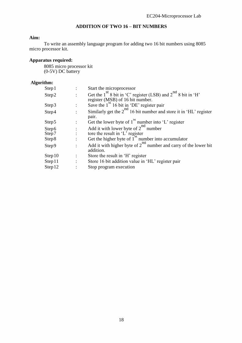
ADDITION OF TWO 16 – BIT NUMBERS
Aim: To write an assembly language program for adding two 16 bit numbers using 8085
micro processor kit.
Apparatus required: 8085 micro processor kit (0-5V) DC battery
Algorithm:
Step 1 : Start the microprocessor
Step 2 : Get the 1st
8 bit in „C‟ register (LSB) and 2nd
8 bit in „H‟ register (MSB) of 16 bit number.
Step 3 : Save the 1st
16 bit in „DE‟ register pair
Step 4 : Similarly get the 2nd
16 bit number and store it in „HL‟ register pair.
Step 5 : Get the lower byte of 1st
number into „L‟ register
Step 6 : Add it with lower byte of 2nd
number Step 7 : tore the result in „L‟ register Step 8 : Get the higher byte of 1
st number into accumulator
Step 9 : Add it with higher byte of 2nd
number and carry of the lower bit addition.
Step 10 : Store the result in „H‟ register
Step 11 : Store 16 bit addition value in „HL‟ register pair
Step 12 : Stop program execution 18

EC204-Microprocessor Lab
START
C = 00H
Load „HL‟ with 1st
Data
Transfer HL - DE
Load „HL‟ with 2nd
Data
DE + HL = HL
If Cy =0
C = C + 01
Store „HL‟ in memory (SUM)
Transfer C - A Store „A‟ in memory (Cy)
STOP
19

EC204-Microprocessor Lab
Address Label Mnemonics Hex Code Comments
4500 MVI C,00 0E C = 00H
4501 00
4502 LHLD 4800 2A HL – 1st
No.
4503 00
4504 48
4505 XCHG EB HL – DE
4506 LHLD 4802 2A HL – 2nd
No.
4507 02
4508 48
4509 DAD D 19 Double addition DE +
HL
450A JNC Ahead D2 If Cy = 0, G0 to 450E 450E
450B 0E
450C 45
450D INR C 0C C = C + 01
450E AHEAD SHLD 4804 22 HL – 4804 (sum)
450F 04
4510 48
4511 MOV C,A 79 Cy – A
4512 STA 4806 32 Cy – 4806
4513 06
4514 48
4515 HLT 76 Stop excution
Input
Without
Input Address Value
4800 01 (addend)
4801 04
4802 02 (augend)
4803 03 (augend)
Output
Output Address Value
4804 03 (sum)
4805 07 (sum)
4806 00 (carry)
Calculation 0000 0100 0000 0001
0000 0011 0000 0010
---------------------------------
0000 0111 0000 0011
0 7 0 3
20

EC204-Microprocessor Lab
With carry
Input Address Value
4800 FF (addend)
4801 DE (addend)
4802 96 (augend)
4803 DF (augend)
Output Address Value
4804 95 (sum)
4805 BE (sum)
4806 01 (carry)
Calculation 1101 1110 1111 1111
1101 1111 1001 0101
---------------------------------
1011 1110 1001 0101
B E 9 5 Result:
The assembly language program for addition of two 16 bit numbers was executed using 8085 micro processing kit.
21
EC204-Microprocessor Lab
SUBTRACTION OF TWO 16 – BIT NUMBERS
Aim: To write an assembly language program for subtracting two 16 bit numbers using
8085 microprocessor kit.
Apparatus required: 8085 microprocessor kit (0-5V) DC battery
Algorithm:
Step 1 : Start the microprocessor
Step 2 : Get the 1st
16 bit in „HL‟ register pair
Step 3 : Save the 1st
16 bit in „DE‟ register pair
Step 4 : Get the 2nd
16 bit number in „HL‟ register pair
Step 5 : Get the lower byte of 1st
number
Step 6 : Get the subtracted value of 2nd
number of lower byte by
subtracting it with lower byte of 1st
number Step 7 : Store the result in „L‟ register Step 8 : Get the higher byte of 2
nd number
Step 9 : Subtract the higher byte of 1st
number from 2nd
number with borrow
Step 10 : Store the result in „HL‟ register
Step 11 : Stop the program execution
22

EC204-Microprocessor Lab
START
C = 00H
Load „HL‟ with 1st
Data
Transfer HL - DE
Load „HL‟ with 2nd
Data
Transfer E – A (LSB)
A = A – L (LSB)
Store „A‟ in memory (LSB)
Transfer D – A (MSB) A – A – H – Borrow (MSB) Store „A‟ in memory (MSB)
STOP
23

EC204-Microprocessor Lab
Address Label Mnemonics Hex Code Comments
4500 MVI C,00 0E C = 00H
4501 00
4502 LHLD 4800 2A L – 1st
No.
4503 00
4504 48
4505 XLHG EB HL – DE
4506 LHLD 4802 2A HL – 2nd
No.
4507 02
4508 48
4509 MOV A,E 7B LSB of „1‟ to „A‟
450A SUB L 95 A – A – L
450B STA 4804 32 A – memory
450C 04
450D 48
450E MOV A,D 7A MSB of 1 to A
450F SBB H 9C A- A – H
4510 STA 4805 32 A – memory
4511 05
4512 48
4513 HLT 76 Stop execution
Input
Without borrow
Input Address Value
4800 07
4801 08
4802 05
4803 06
Output
Output Address Value
4804 02
4805 02
4807 00
24

EC204-Microprocessor Lab
With borrow
Input Address Value
4800 05
4801 06
4802 07
4803 08
Output Address Value
4804 02
4805 02
4806 01
Calculation
05 06 - 07 08
05 06 0101 0110 07 08 0111 1000
CMA 1010 1001 CMA 1000 0111
ADI 0000 0001 ACI 0000 0001
--------------- --------------
1010 1010 1000 1000
05 06 + 07 08
1010 1010
1000 1000
---------------
(1) 0010 0010
02 02 Result:
The assembly language program for subtraction of two 16 bit numbers was executed by using 8085 micro processing kit.
25

EC204-Microprocessor Lab MULTIPLICATION OF TWO 8 – BIT NUMBERS
Aim: To write an assembly language for multiplying two 8 bit numbers by using 8085
micro processor kit.
Apparatus required: 8085 microprocessor kit (0-5V) DC battery
Algorithm:
Step 1 : Start the microprocessor
Step 2 : Get the 1st
8 bit numbers
Step 3 : Move the 1st
8it number to register „B‟
Step 4 : Get the 2nd
8 bit number
Step 5 : Move the 2nd
8 bit number to register „C‟ Step 6 : Intialise the accumulator as zero Step 7 : Intialise the carry as zero
Step 8 : Add both register „B‟ value as accumulator
Step 9 : Jump on if no carry
Step 10 : Increment carry by 1 if there is
Step 11 : Decrement the 2nd
value and repeat from step 8, till the 2nd
value becomes zero.
Step 12 : Store the multiplied value in accumulator
Step 13 : Move the carry value to accumulator
Step 14 : Store the carry value in accumulator 26

EC204-Microprocessor Lab
START
Get the 1st
8 bit number
Move it to register „B‟
Get the 2nd
8 bit number Intialize the accumulator as zero & carry as zero
Add the accumulator with 1st
number
No Check for
carry?
Yes
Increment carry
Decrement 2nd
number
No 2nd
Number
Yes
Store the value f carry in accumulator
END
27

EC204-Microprocessor Lab
Address Label Mnemonics Hex Code Comments
4100 LDA 4500 3A, 00, 45 Load the first 8 bit number
4103 MOV B,A 47 Move the 1st
8 bit data to register „B‟
4104 LDA 4501 3A, 01, 45 Load the 2nd
16 it number
4107 MOV C,A 4F Move the 2nd
8 bit data to register „C‟
4108 MVI A, 00 3E, 00 Intialise the accumulator as zero
410A MVI D, 00 16, 00 Intialise the carry as zero
410C ADD B 80 Add the contents of „B‟ and
accumulator
410D INC D2 11, 41 Jump if no carry
4110 INR D 14 Increment carry if there is
4111 DCR C OD Decrement the value „C‟
4112 JNZ C2 0C, 41 Jump if number zero
4115 STA 4502 32 02, 45 Store the result in accumulator
4118 MOV A,D 7A Move the carry into
accumulator
4119 STA 4503 32,03,45 Store the result in
accumulator
411C HLT 76 Stop the program execution
Input
Input Address Value
4500 04
4501 02
Output
Output Address Value
4502 08
4503 00 Result:
The assembly language program for multiplication of two 8 bit numbers was executed using 8085 micro processing kit.
28

EC204-Microprocessor Lab
DIVISION OF TWO 8 – BIT NUMBERS
Aim: To write an assembly language program for dividing two 8 bit numbers using
microprocessor kit.
Apparatus required: 8085 microprocessor kit (0-5V) DC battery
Algorithm:
Step 1 : Start the microprocessor Step 2 : Intialise the Quotient as zero
Step 3 : Load the 1st
8 bit data Step 4 : Copy the contents of accumulator into register „B‟
Step 5 : Load the 2nd
8 bit data Step 6 : Compare both the values Step 7 : Jump if divisor is greater than dividend
Step 8 : Subtract the dividend value by divisor value
Step 9 : Increment Quotient
Step 10 : Jump to step 7, till the dividend becomes zero
Step 11 : Store the result (Quotient) value in accumulator
Step 12 : Move the remainder value to accumulator
Step 13 : Store the result in accumulator
Step 14 : Stop the program execution
29
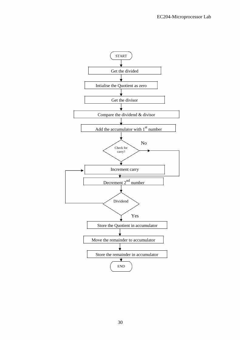
EC204-Microprocessor Lab
START
Get the divided
Intialise the Quotient as zero
Get the divisor
Compare the dividend & divisor
Add the accumulator with 1st
number
No Check for
carry?
Increment carry
Decrement 2nd
number
Dividend
Yes
Store the Quotient in accumulator Move the remainder to accumulator
Store the remainder in accumulator
END
30
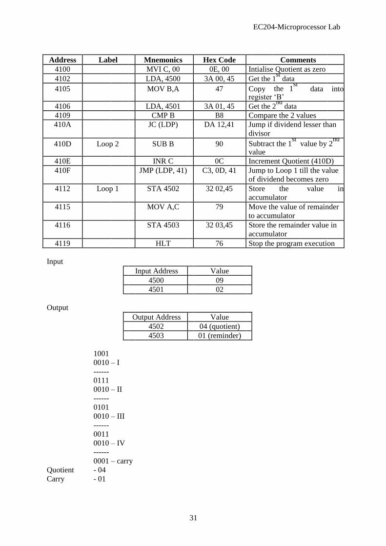
EC204-Microprocessor Lab
Address Label Mnemonics Hex Code Comments
4100 MVI C, 00 0E, 00 Intialise Quotient as zero
4102 LDA, 4500 3A 00, 45 Get the 1st
data
4105 MOV B,A 47 Copy the 1st
data into register „B‟
4106 LDA, 4501 3A 01, 45 Get the 2nd
data
4109 CMP B B8 Compare the 2 values
410A JC (LDP) DA 12,41 Jump if dividend lesser than
divisor
410D Loop 2 SUB B 90 Subtract the 1st
value by 2nd
value
410E INR C 0C Increment Quotient (410D)
410F JMP (LDP, 41) C3, 0D, 41 Jump to Loop 1 till the value of dividend becomes zero
4112 Loop 1 STA 4502 32 02,45 Store the value in accumulator
4115 MOV A,C 79 Move the value of remainder to accumulator
4116 STA 4503 32 03,45 Store the remainder value in accumulator
4119 HLT 76 Stop the program execution
Input
Input Address Value
4500 09
4501 02
Output
Output Address Value
4502 04 (quotient)
4503 01 (reminder)
1001
0010 – I
------
0111
0010 – II
------
0101
0010 – III
------
0011
0010 – IV
------
0001 – carry
Quotient - 04
Carry - 01
31

EC204-Microprocessor Lab
Result: The assembly language program for division of two 8 bit numbers was executed using
8085 micro processing kit.
32

EC204-Microprocessor Lab
ASCENDING ORDER
Aim: To write a program to sort given „n‟ numbers in ascending order
Apparatus required: 8085 microprocessor kit (0-5V) DC battery
Algorithm:
Step 1 : Start the microprocessor Step 2 : Accumulator is loaded with number of values to sorted and it is
saved
Step 3 : Decrement 8 register (N-1) Repetitions)
Step 4 : Set „HL‟ register pair as data array
Step 5 : Set „C‟ register as counter for (N-1) repetitions
Step 6 : Load a data of the array in accumulator
Step 7 : Compare the data pointed in „HL‟ pair
Step 8 : If the value of accumulator is smaller than memory, then jump
to step 10.
Step 9 : Otherwise exchange the contents of „HL‟ pair and accumulator
Step 10 : Decrement „C‟ register, if the of „C‟ is not zero go to step 6
Step 11 : Decrement „B‟ register, if value of „B‟ is not zero, go step 3
Step 12 : Stop the program execution
33

EC204-Microprocessor Lab
START
Load the count value in accumulator and save it in register „B‟
Decrement „B‟ register (N-1)
Load the starting address of array in „HL‟
Decrement „C‟ register of array in „HL‟
Increment the data pointer
Compare the data pointed by „HL‟ with „A‟ Compare the datas
A<M
No
Exchange the contents of
Yes
memory pointer by „HL‟
C=0? Increment carry by one
No
Yes
Decrement register „B‟ No
B=0?
END
34
EC204-Microprocessor Lab
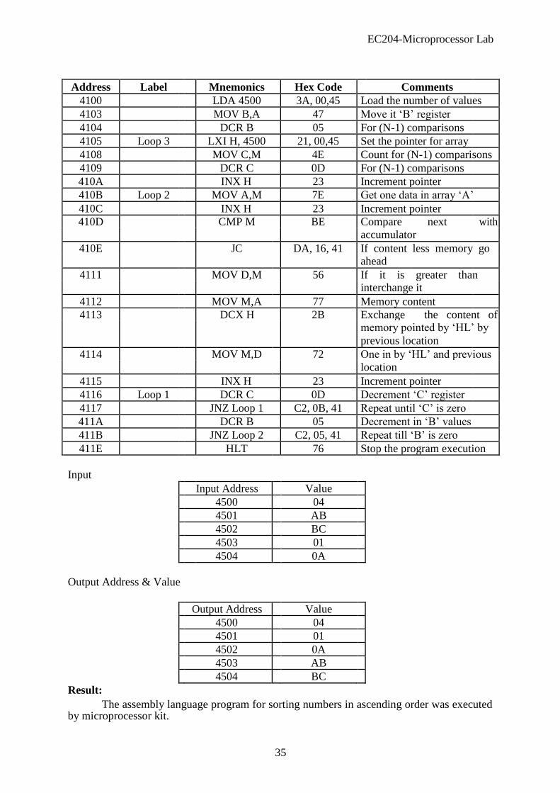
Address Label Mnemonics Hex Code Comments
4100 LDA 4500 3A, 00,45 Load the number of values
4103 MOV B,A 47 Move it „B‟ register
4104 DCR B 05 For (N-1) comparisons
4105 Loop 3 LXI H, 4500 21, 00,45 Set the pointer for array
4108 MOV C,M 4E Count for (N-1) comparisons
4109 DCR C 0D For (N-1) comparisons
410A INX H 23 Increment pointer
410B Loop 2 MOV A,M 7E Get one data in array „A‟
410C INX H 23 Increment pointer
410D CMP M BE Compare next with
accumulator
410E JC DA, 16, 41 If content less memory go ahead
4111 MOV D,M 56 If it is greater than interchange it
4112 MOV M,A 77 Memory content
4113 DCX H 2B Exchange the content of memory pointed by „HL‟ by
previous location
4114 MOV M,D 72 One in by „HL‟ and previous
location
4115 INX H 23 Increment pointer
4116 Loop 1 DCR C 0D Decrement „C‟ register
4117 JNZ Loop 1 C2, 0B, 41 Repeat until „C‟ is zero
411A DCR B 05 Decrement in „B‟ values
411B JNZ Loop 2 C2, 05, 41 Repeat till „B‟ is zero
411E HLT 76 Stop the program execution
Input
Input Address Value
4500 04
4501 AB
4502 BC
4503 01
4504 0A
Output Address & Value
Output Address Value
4500 04
4501 01
4502 0A
4503 AB
4504 BC
Result: The assembly language program for sorting numbers in ascending order was executed
by microprocessor kit.
35

EC204-Microprocessor Lab DESCENDING ORDER
Aim: To write a program to sort given „n‟ numbers in descending order
Apparatus required: 8085 microprocessor kit (0-5V) DC battery
Algorithm:
Step 1 : Start the microprocessor Step 2 : Load the number of values into accumulator and save the
number of values in register „B‟
Step 3 : Decrement register „B‟ for (N-1) Repetitions
Step 4 : Set „HL‟ register pair as data array address pointer and load the
data of array in accumulator
Step 5 : Set „C‟ register as counter for (N-1) repetitions
Step 6 : Increment „HL‟ pair (data address pointer)
Step 7 : Compare the data pointed by „HL‟ with accumulator
Step 8 : If the value of accumulator is larger than memory, then jump
to step 10, otherwise next step.
Step 9 : Exchange the contents of memory pointed by „HL‟ and
accumulator
Step 10 : Decrement „C‟ register, if the of „C‟ is not zero go to step 6,
otherwise next step.
Step 11 : Decrement „B‟ register, if „B‟ is not zero, go step 3, otherwise
next step.
Step 12 : Stop the program execution 36

EC204-Microprocessor Lab
START
Load the count value to accumulator
Save the value in „B‟ register
Decrement „B‟ register (N-1)
Load the starting address of data array in „HL‟ pair
Using data pointer, load the count value in „C‟
Decrement „C‟ register (counter for N-1)
Increment the data pointer „HL‟ with „A‟
Compare the data pointed at „HL‟ with „A‟
A<M No
Exchange the contents
C=0? Decrement register C
Yes
Decrement register „C‟
No
B=0? No Yes
END
37

EC204-Microprocessor Lab
Address Label Mnemonics Hex Code Comments
4100 LDA 4500 3A, 00,45 Load the number of values
in accumulator
4103 MOV B,A 47 Move it to „B‟ register
4104 DCR B 05 For (N-1) comparisons
4105 Loop 3 LXI H, 4500 21, 00,45 Set the pointer for array
4108 MOV C,M 4E Count for (N-1) comparisons
4109 DCR C 0D For (N-1) comparisons
410A INX H 23 Increment pointer
410B Loop 2 MOV A,M 7E Get one data from array
410C INX H 23 Increment pointer
410D CMP M BE Compare next with number
410E ICE, Loop 1 D2, 16,41 If content „A‟ is greater than
content of „HL‟ pair
4111 MOV D,M 56 If it is greater than
interchange the datas
4112 MOV M,A 77 Accumulator to memory
value
4113 DCX H 2B Decrement memory pointer
4114 MOV M,D 72 Move the old to „HL‟ and previous location
4115 INX H 23 Increment pointer
4116 Loop 1 DCR C 0D Decrement „C‟ register
4117 JNZ Loop 2 C2, 0B, 41 Repeat till „C‟ is zero
411A DCR B 05 Decrement in „B‟ values
411B JNZ Loop 3 C2, 05, 41 Jump to loop till the value of
„B‟ be
411E HLT 76 Stop the program execution
Input
Input Address Value
4500 04
4501 AB
4502 BC
4503 01
4504 0A
Output Address & Value
Output Address Value
4500 04
4501 BC
4502 AB
4503 0A
4504 01
Result: The assembly language program for sorting „4‟ numbers in descending order was
executed successfully using microprocessor kit.
38

EC204-Microprocessor Lab
SUM OF DATAS
Aim: To write an assembly language program to calculate the sum of datas using 8085
microprocessor kit.
Apparatus required: 8085 microprocessor kit (0-5V) DC battery
Algorithm:
Step 1 : Start the microprocessor Step 2 : Load the number of values in series in accumulator and move it
to register C and load the starting address of array
Step 3 : Intialize the value of A as „00‟
Step 4 : Move the value of „A‟ to „B‟ register
Step 5 : Add the content of accumulator with the data pointed by „HL‟
pair
Step 6 : If there exists a carry, increment „B‟ by 1, if not continue
Step 7 : Increment the pointer to next data
Step 8 : Decrement the value of „C‟ by 1, which is used as counter
Step 9 : If „C‟ is equal to zero, go to step 10 if not go to step 5.
Step 10 : Store the value of „A‟ to memory, it shows the result
Step 11 : Move the content of B to A
Step 12 : Store the value of A to memory
Step 13 : Stop the program 39
EC204-Microprocessor Lab
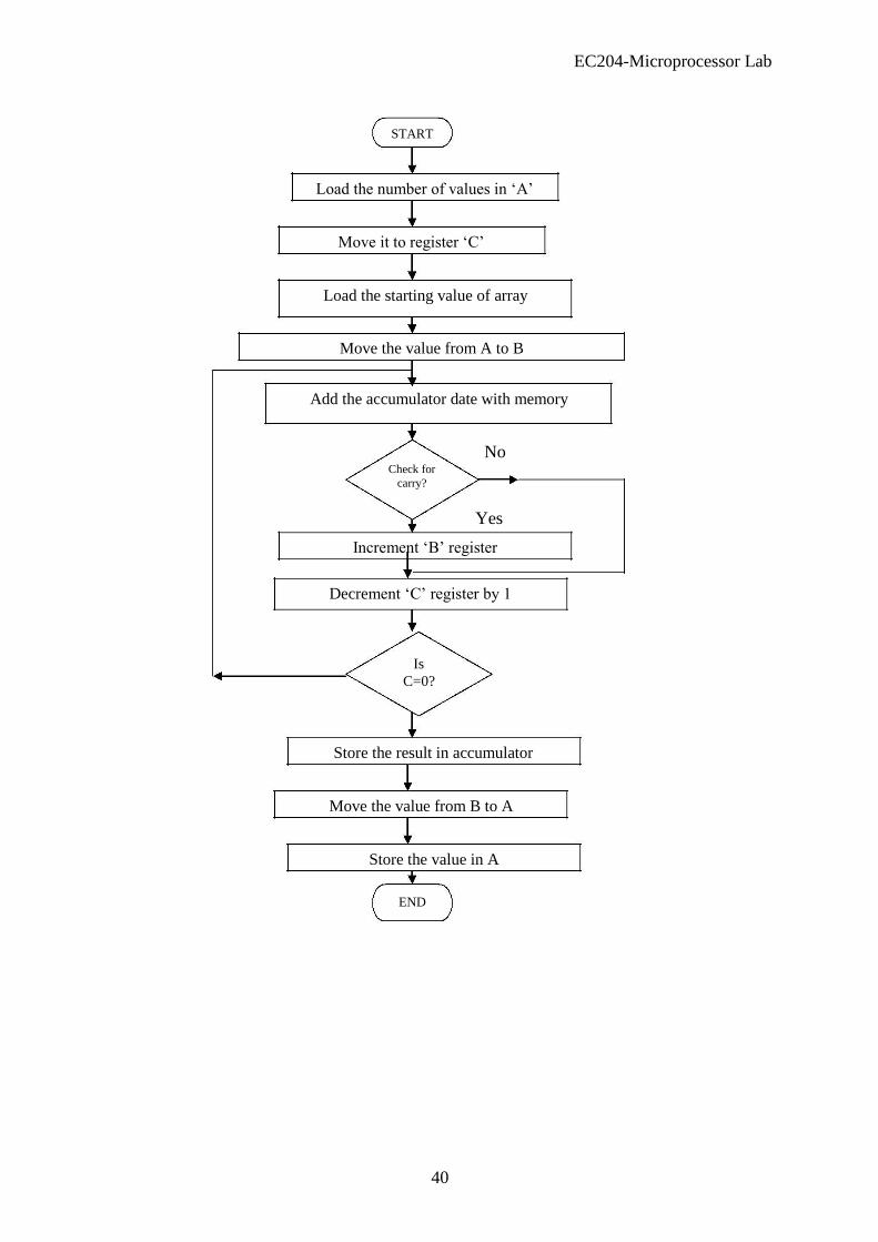
START
Load the number of values in „A‟
Move it to register „C‟
Load the starting value of array
Move the value from A to B Add the accumulator date with memory
No Check for
carry?
Yes
Increment „B‟ register
Decrement „C‟ register by 1
Is
C=0?
Store the result in accumulator
Move the value from B to A
Store the value in A
END
40

EC204-Microprocessor Lab
Address Label Mnemonics Hex Code Comments
4100 LDA 4200 3A 00,42 Load the accumulator with
number of values
4103 MOV B,A 4F Move it from A to C
4104 LXI H, 4201 21,01,42 Load the starting address of data array
4107 SUB A 97 Intialise „A‟ as 00
4108 MOV B,A 47 Intialise „B‟ as 00
4109 Loop ADD M 86 Add the previous sum with
next data
410A JNC Skip D2, 0E, 41 Jump on if no carry
410D INR B 04 Increment carry by one
410E Skip INX H 23 Increment pointer for next data
410F DCR C 0D Decrement „C‟ by one
4110 JNZ Loop C2, 09, 41 Jump if not zero
4113 STA 4400 32,00,44 Store the sum in accumulator
4116 MOV A,B 78 Move the value of carry to A
from B
4117 STA 4401 32,01,44 Store the carry in memory
411A HLT 76 End of program
Input
Input Address Value
4200 04
4201 07
4202 09
4203 03
4204 04
Output
Output Address Value
4400 17
4401 00
07 + 09 + 03 + 04 = 23
= 17 (in Hexa decimal)
(0F + 8 = 233)
0F = 0000 1111
08 = 0000 1000
---------------
0001 0111
1 7
41

EC204-Microprocessor Lab
Result: The assembly language program for sum of datas was executed successfully using
8085 microprocessor kit. 42
EC204-Microprocessor Lab
FACTORIAL OF 8 BIT NUMBER
Aim: To write an program to calculate the factorial of a number (between 0 to 8)
Apparatus required: 8085 microprocessor kit (0-5V) power supply
Algorithm:
Step 1 : Intialize the stack pointer Step 2 : Get the number in accumulator
Step 3 : Check for if the number is greater than 1. If no store the result
otherwise go to next step.
Step 4 : Load the counter and initialize result
Step 5 : Now factorial program in sub-routine is called.
Step 6 : In factorial,
initialize HL RP with 0. Move the count value to B
Add HL content with Rp. Decrement count (for multiplication)
Step 7 : Exchange content of Rp (DE) with HL.
Step 8 : Decrement counter (for factorial) till zero flag is set.
Step 9 : Store the result
Step 10 : Hault
Memory address Content
4250 05
4251 (12010) 43

EC204-Microprocessor Lab
START
Intialize stack pointer
Get the number
If Number < 2 ?
Result = 1
Load counter Initialize result
CALL facto
END
44

EC204-Microprocessor Lab
Facto
Result = Result X no
No = No -1 No
If No = 0 ?
Yes
RET 45

EC204-Microprocessor Lab
Memory Hex Code Label Mnemonics Comments
Location Op code Operand
4200 3A LDA 4250 Get the number in 4201 50 accumulator
4202 42
4203 FE CPI 02H Compare data with 2 4204 02 and check it is greater
than 1
4205 DA JC Loop 1 If cy =1 jump to loop 1 4206 17 If cy = 0 proceed
4207 42
4208 5F MOV E,A Move content of A to E
4209 16 MVI D,00 Load this term as a
420A 00 result
420B 3D DCR A Decrement
accumulator by 1
420C 4F MOV C,A Move „A‟ content to „C‟ (counter 1 less than
A)
420D CD CALL Facto Call sub routine 420E 00 programe Facto
420F 46
4210 EB XCHG Exchange (DE) – (HL)
4211 22 SHLD 4251 Store content of HL in 4212 51 specified memory
4213 42 location
4214 C3 JMP Loop 3 Jump to Loop 3
4215 1D
4216 42
4217 21 Loop 1 LXI H,0001H HL is loaded with data 4218 00 01
4219 01
421A 22 SHLD 4251 Store the result in 421B 51 memory
421C 42
421D 76 Loop 3 HLT Terminate the program
Sub Routine
4600 21 Facto LXI H,0000 Initialize HL pair
4601 00
4602 00
4603 41 MOV B,C Content of „C‟ is moved to B
4604 19 Loop 2 DAD D Content of DE is added with HL
4605 05 DCR B „B‟ is decremented
4606 C2 JNZ Loop 2 Multiply by successive 4607 04 addition till zero flag is
4608 46 set 46

EC204-Microprocessor Lab
4609 EB XCHG [DE] – [HL]
460A 0D DCR C Decrement counter value
460B C4 CNZ Facto Call on no zero to facto 460C 00 (i.e repeat process till
460D 46 zero flag for c = 1)
460E C9 RET Return to main program
Memory address Content
4250 04
4251 18
1 x 2 x 3 x 4 = 24 Hexadecimal
16 24 1-8
Result:
Thus, factorial program was done successfully
47

EC204-Microprocessor Lab
FIBANOCCI SERIES
Aim: To write an assembly language program to displace Fibanocci Series.
Apparatus required: 8085 microprocessor kit (0-5V) DC battery
Algorithm:
Step 1 : Start the microprocessor Step 2 : Load the length of series in the accumulator and decrement it
by 2
Step 3 : Move the value to register „D‟
Step 4 : Load the starting value of data value address
Step 5 : Intialise the 1st
number as 00
Step 6 : Move the pointer to 2nd
data and intialise them as „01‟ Step 7 : Move the pointer to next position for next data Step 8 : Intialise B as „00‟ and C as „01‟ for calculations
Step 9 : Copy the contents of „B‟ to accumulator
Step 10 : Add the content of „C‟ register to accumulator
Step 11 : Move the content „C‟ to „B‟ and „A‟ to C
Step 12 : Now store the result to memory pointed by „HL‟ pair
Step 13 : Move the pointer to next pointer
Step 14 : Decrement 0 by 1 for counter
Step 15 : If „D‟ is not zero, go to step 9
Step 16 : if „D‟ is zero, end the program
48

EC204-Microprocessor Lab
START
Load the lenth of series
Decrement it by 2
Move it to „D‟ register
Load the starting value of data
Intialise their values as „00‟
Move the pointer to next position
Intialise the value as „01‟
Move the pointer to next position
Intialise „B‟ as „00‟ & „C‟ as „01‟
Move it from „B‟ to „A‟
Store the result in accumulator
Move the pointer to next position
Decrement D by 1 No
Check D=0?
Yes
END
49

EC204-Microprocessor Lab
Address Label Mnemonics Hex Code Comments
4200 LDA 4300 3A, 00, 43 Store the length of series in
„A‟
4203 SUI 02 D6, 02 Decrement „A‟ by 02
4205 MOV D,A 57 Move „A‟ to „D‟ (counter)
4206 LXI H, 4301 21,01,43 Load the starting address of array
4209 MVI M,00 36,00 Intialise 4301 as „00‟
420B INX H 23 Increment pointer
420C MVI M, 01 36,01 Initialize 2nd
as „01‟
420E INX H 23 Increment pointer
420F MVI B,00 06,00 Intialise „B‟ as „00‟
4211 MVI, C, 01 0E, 01 Intialise „C‟ as „01‟
4213 Loop MOV A,B 78 Move B to A
4214 ADD C 81 Add „A‟ and „C‟
4215 MOV B,C 41 Move C to B
4216 MOV C,A 4F Move A to C
4217 MOV M,A 77 Move the result to memory
4218 INX H 23 Increment pointer
4219 DCR D 15 Decrement counter
421A JNZ loop C2, 13,42 If D = 0, jump to loop
421D HLT 76 Stop the program
Input
Input Address Value
4300 05
Output
Output Address Value
4301 00
4302 01
4303 01
4304 02
4305 03
00 + 01 = 01
01+ 01 = 02
02 + 01 = 03
Result: The assembly language for Fibonaci series was executed successfully using 8085
microprocessor kit.
50
EC204-Microprocessor Lab
16 – BIT MULTIPLICATION
Aim: To write an assembly language program for 16 bit multiplication by using 8085
microprocessor kit.
Apparatus required: 8085 microprocessor kit (0-5V) DC battery
Algorithm:
Step 1 : Start the microprocessor
Step 2 : Load the 1st
data in „HL‟ register pair Step 3 : Move content of „HL‟ pair to stack pointer
Step 4 : Load the 2nd
data in „HL‟ and move it to „DE‟ Step 5 : Make „HL‟ pair as „00‟ and „00‟ Step 6 : Add „HL‟ pair and „SP‟
Step 7 : Check for carry condition, if carry is present increment it by
one else move to next step.
Step 8 : Decrement DE register
Step 9 : Then move E to „A‟ and perform „OR‟ operation with „a‟ and
„D‟
Step 10 : The value of operation is zero, then store the value else go to
step 3
Step 11 : Stop the program
51
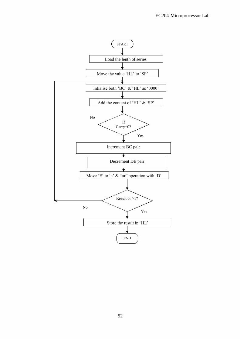
EC204-Microprocessor Lab
START
Load the lenth of series
Move the value „HL‟ to „SP‟
Intialise both „BC‟ & „HL‟ as „0000‟
Add the content of „HL‟ & „SP‟
No If
Carry=0?
Yes
Increment BC pair
Decrement DE pair
Move „E‟ to „a‟ & “or” operation with „D‟
Result or ≥1? No
Yes
Store the result in „HL‟
END
52
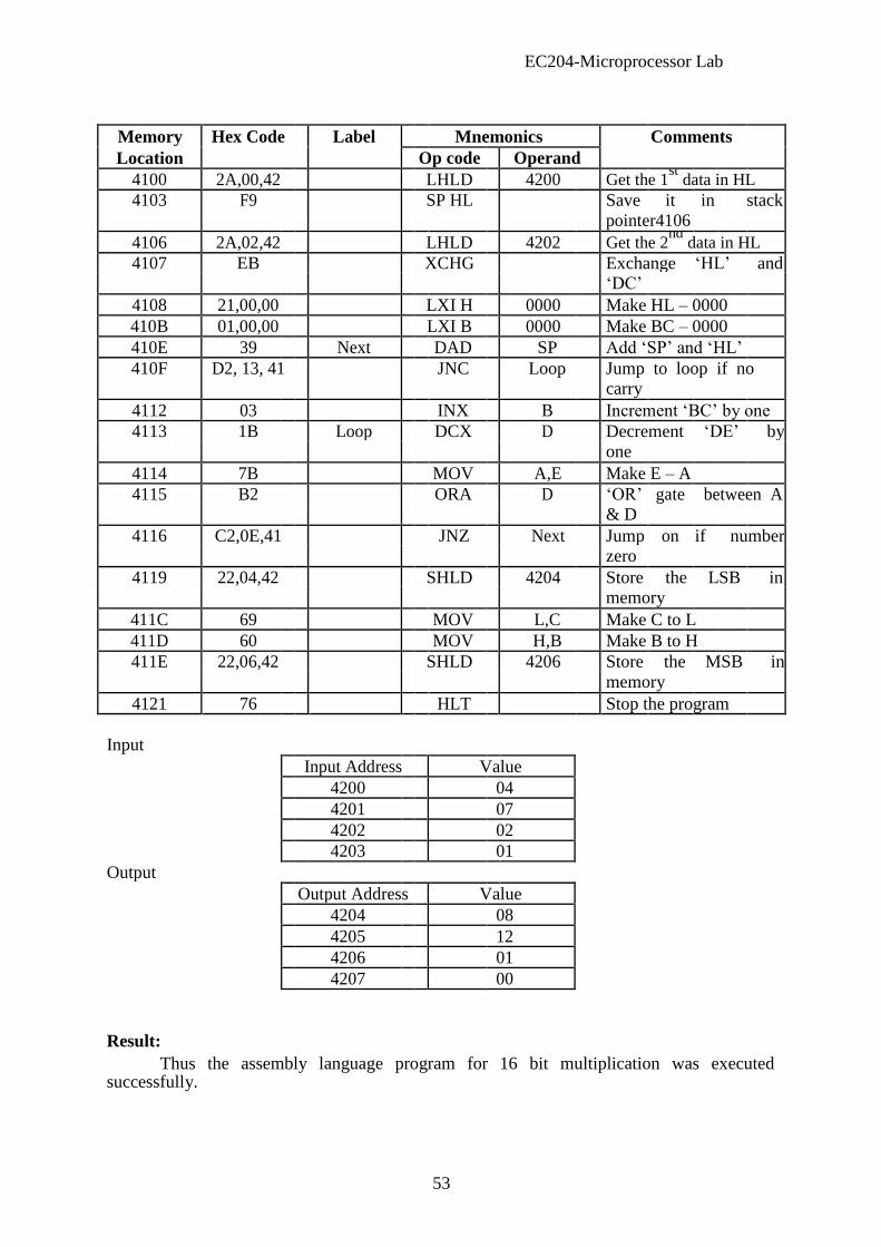
EC204-Microprocessor Lab
Memory Hex Code Label Mnemonics Comments
Location Op code Operand
4100 2A,00,42 LHLD 4200 Get the 1st
data in HL
4103 F9 SP HL Save it in stack
pointer4106
4106 2A,02,42 LHLD 4202 Get the 2nd
data in HL
4107 EB XCHG Exchange „HL‟ and „DC‟
4108 21,00,00 LXI H 0000 Make HL – 0000
410B 01,00,00 LXI B 0000 Make BC – 0000
410E 39 Next DAD SP Add „SP‟ and „HL‟
410F D2, 13, 41 JNC Loop Jump to loop if no carry
4112 03 INX B Increment „BC‟ by one
4113 1B Loop DCX D Decrement „DE‟ by
one
4114 7B MOV A,E Make E – A
4115 B2 ORA D „OR‟ gate between A & D
4116 C2,0E,41 JNZ Next Jump on if number zero
4119 22,04,42 SHLD 4204 Store the LSB in memory
411C 69 MOV L,C Make C to L
411D 60 MOV H,B Make B to H
411E 22,06,42 SHLD 4206 Store the MSB in
memory
4121 76 HLT Stop the program
Input
Input Address Value
4200 04
4201 07
4202 02
4203 01
Output
Output Address Value
4204 08
4205 12
4206 01
4207 00
Result: Thus the assembly language program for 16 bit multiplication was executed
successfully.
53

EC204-Microprocessor Lab 16 – BIT DIVISION
Aim: To write an assembly language program for 16 bit division in 8085 microprocessor.
Apparatus required: 8085 microprocessor kit (0-5V) DC battery
Algorithm:
Step 1 : Start the microprocessor Step 2 : Intialise „BC‟ as „0000‟ for Quotient
Step 3 : Load the divisor in „HL‟ pair and save it in „DE‟ register pair
Step 4 : Load the dividend in „HL‟ pair
Step 5 : Move the value of „a‟ to register „E‟
Step 6 : Subtract the content of accumulator with „E‟ register
Step 7 : Move the content „A‟ to „C‟ & „H‟ to „A‟
Step 8 : Subtract with borrow, the content of „A‟ with „D‟
Step 9 : Move the value of „a‟ to „H‟
Step 10 : If cy = 1, go to step 12, otherwise next step
Step 11 : Increment „B‟ register & jump to step „4‟
Step 12 : Add both contents of „DC‟ and „HL‟
Step 13 : Store the remainder in memory
Step 14 : Move the content of „C‟ to „L‟ & „B‟ to „H‟
Step 15 : Store the Quotient in memory
Step 16 : Stop the program 54

EC204-Microprocessor Lab
START
Intialise the Quotient as zero
Load the divisor in „HL‟ & move it „DE‟
Load the dividend in „HL‟ pair
Intialise A with compare „E‟ & „L‟
Transfer and Add the contents of A and B
Check for if cy = 1
Yes
Subtract „HL‟ from
„DE‟ increment BC pair
Store te remainder in HL in memory Move the content of BC to „HL‟ pair Store the Quotient in HL to memory
END 55
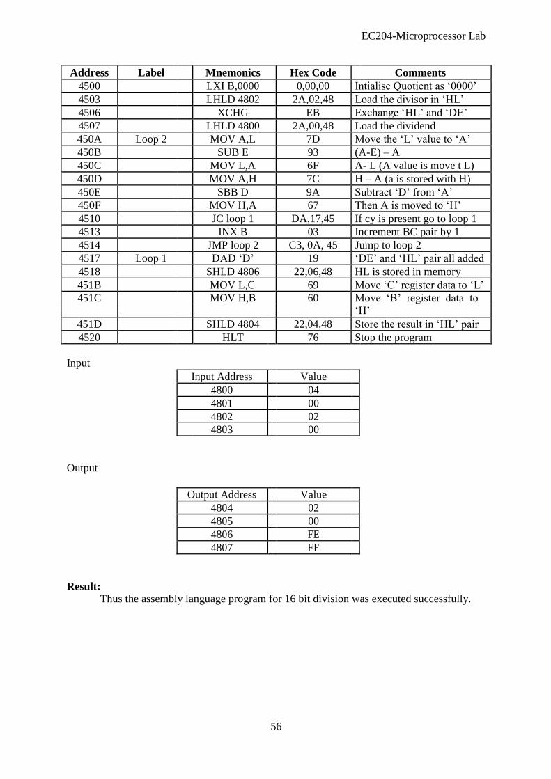
EC204-Microprocessor Lab
Address Label Mnemonics Hex Code Comments
4500 LXI B,0000 0,00,00 Intialise Quotient as „0000‟
4503 LHLD 4802 2A,02,48 Load the divisor in „HL‟
4506 XCHG EB Exchange „HL‟ and „DE‟
4507 LHLD 4800 2A,00,48 Load the dividend
450A Loop 2 MOV A,L 7D Move the „L‟ value to „A‟
450B SUB E 93 (A-E) – A
450C MOV L,A 6F A- L (A value is move t L)
450D MOV A,H 7C H – A (a is stored with H)
450E SBB D 9A Subtract „D‟ from „A‟
450F MOV H,A 67 Then A is moved to „H‟
4510 JC loop 1 DA,17,45 If cy is present go to loop 1
4513 INX B 03 Increment BC pair by 1
4514 JMP loop 2 C3, 0A, 45 Jump to loop 2
4517 Loop 1 DAD „D‟ 19 „DE‟ and „HL‟ pair all added
4518 SHLD 4806 22,06,48 HL is stored in memory
451B MOV L,C 69 Move „C‟ register data to „L‟
451C MOV H,B 60 Move „B‟ register data to „H‟
451D SHLD 4804 22,04,48 Store the result in „HL‟ pair
4520 HLT 76 Stop the program
Input
Input Address Value
4800 04
4801 00
4802 02
4803 00
Output
Output Address Value
4804 02
4805 00
4806 FE
4807 FF
Result: Thus the assembly language program for 16 bit division was executed successfully.
56

EC204-Microprocessor Lab
BINARY TO BCD CONVERSION
Aim: To write an assembly language program to convert an 8 bit binary data to BCD using
8085 microprocessor kit.
Apparatus required: 8085 microprocessor kit (0-5V) power supply
Algorithm:
Step 1 : Start the microprocessor Step 2 : Clear „D‟ and „E‟ register to account for hundred‟s and ten‟s
load the binary data in accumulator
Step 3 : Compare „A‟ with 64 if cy = 01, go step C otherwise next step
Step 4 : Subtract 64 from (64+1) „A‟ register
Step 5 : Increment „E‟ register
Step 6 : Compare the register „A‟ with „0A‟, if cy=1, go to step 11,
otherwise next step
Step 7 : Subtract (0AH) from „A‟ register Step 8 : Increment D register Step 9 : Go to step 7
Step 10 : Combine the units and tens to from 8 bit result
Step 11 : Save the units, tens and hundred‟s in memory
Step 12 : Stop the program execution
57

EC204-Microprocessor Lab
START
Intialise „D‟ as „00‟ for hundreds and „e‟ as „00‟ for tens
Load the binary data in „A‟
Compare the accumulator with „64‟
Cy = ?
Subratct 64 from accumulator
Increment „E‟ register
Compare with 0A
Cy = ?
Subtract „0A‟ from accumulator
Increment register „D‟
Combine the units & tens to form 8 bit
Save the units, tens & hundreds in memory
END
58

EC204-Microprocessor Lab
Memory Hex Code Label Mnemonics Comments
Location Op code Operand
4100 0E,00 MVI E,00 Clear „E‟ register
(Hund)
4102 53 MOV D,E Clear „D‟ register
(tens)
4103 3A,00,42 LDA 4200 Get the data in „A‟
4106 C3,06,41 HUND CPI 64 Compare the data with
64
4108 DA,11,41 JC TEN If content is less jump
to ten
410B D6, 64 SUI 64 Subtract data by 64
410D IC INR E Increment carry each time
410E C3,06,41 JMP HUND Jump to hundred & repeat
4111 C3, 0A TEN CPI 0A Compare the data with
0A
4113 DA,1C,41 JC UNIT If data is less jump to
unit
4116 D6, 0A SUI 0A Subtract the data by 0A
4118 14 INR D Increment „D‟ each time
4119 C3,11,41 JMP TEN Jump to ten & repeat
411C 4F UNIT MOV 4A Move the value „A‟ to „C‟
411D 7A MOV A,D Move the value „D‟ to „A‟
411E 07 RLC Rotate the value of „A‟
411F 07 RLC Of „A‟ so that
4120 07 RLC Lower and upper niddle
4121 07 RLC Gets exchanged
4122 81 ADD C Add „A‟ and „C‟
4123 32,50,42 STA 42,50 Save ten‟ & units in „M‟
4126 7B MOV A,E Move to E to A
4127 32,51,42 STA 4251 Save hundreds unit in
„A‟
412A 76 HLT Stop the program
execution 59
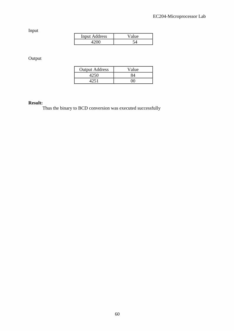
EC204-Microprocessor Lab Input
Input Address Value
4200 54
Output
Output Address Value
4250 84
4251 00 Result:
Thus the binary to BCD conversion was executed successfully
60

EC204-Microprocessor Lab
BCD TO BINARY
Aim: To write an assembly language program to convert BCD data to Binary data using
8085 microprocessor kit.
Apparatus required: 8085 microprocessor kit (0-5V) power supply
Algorithm:
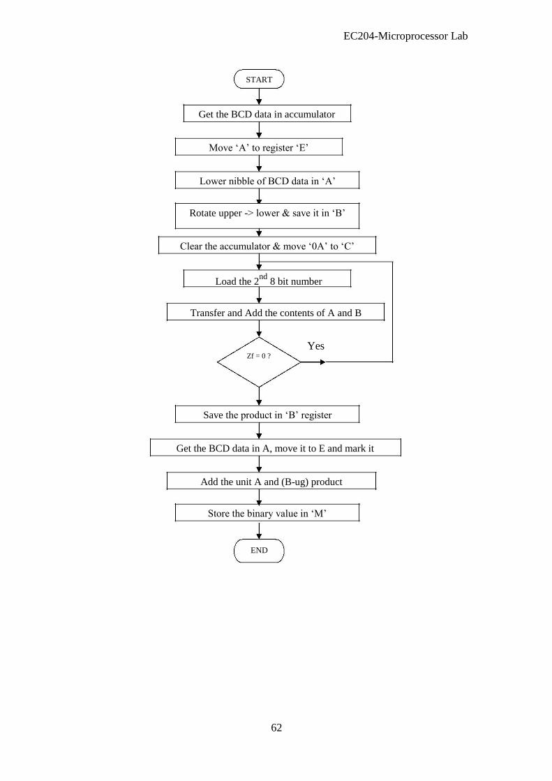
Step 1 : Start the microprocessor Step 2 : Get the BCD data in accumulator and save it in register „E‟
Step 3 : Mark the lower nibble of BCD data in accumulator
Step 4 : Rotate upper nibble to lower nibble and save it in register „B‟
Step 5 : Clear the accumulator
Step 6 : Move 0AH to „C‟ register Step 7 : Add „A‟ and „B‟ register Step 8 : Decrement „C‟ register. If zf = 0, go to step 7
Step 9 : Save the product in „B‟
Step 10 : Get the BCD data in accumulator from „E‟ register and mark
the upper nibble
Step 11 : Add the units (A-ug) to product (B-ug)
Step 12 : Store the binary value in memory
Step 13 : End the program
61
EC204-Microprocessor Lab
START
Get the BCD data in accumulator
Move „A‟ to register „E‟
Lower nibble of BCD data in „A‟
Rotate upper -> lower & save it in „B‟ Clear the accumulator & move „0A‟ to „C‟
Load the 2nd
8 bit number
Transfer and Add the contents of A and B
Yes Zf = 0 ?
Save the product in „B‟ register Get the BCD data in A, move it to E and mark it
Add the unit A and (B-ug) product
Store the binary value in „M‟
END
62

EC204-Microprocessor Lab
Memory Hex Code Label Mnemonics Comments
Location Op code Operand
4100 3A,00,42 LDA 4200 Get the data in „A‟
4103 5E MOV E,A Save in „E‟ register
4104 E6, F0 ANI F0 Mark the lower nibble
4106 07 RLC Rotate the upper
4107 07 RLC To lower nibble
4108 07 RLC And save in
4109 07 RLC Register B
410A 47 MOV B,A Move it from „A‟ to
„B‟
410B AF XRA A Clear the accumulator
410C 0E,0A MVI C,0A Intialise „C‟ as „0A‟
410E 08 REP
410F 0D DCR C Decrement „C‟ register
4110 C2,0E,41 JNZ Jump till value „C‟ is 0
4113 47 MOV B,A Move the value A to B
4114 7B MOV A,E Get the BCD in „A‟
4115 E6, 0F ANI 0F Mark the upper nibble
4117 80 ADD B Add „A‟ and „B‟
4118 32,01,42 STA 4201 Save the binary data
411B 76 HLT Stoptheprogram
execution
Input
Input Address Value
4200 68
Output
Output Address Value
4201 44
16
68
4-4
Result: Thus the BCD to binary conversion was executed successfully
63
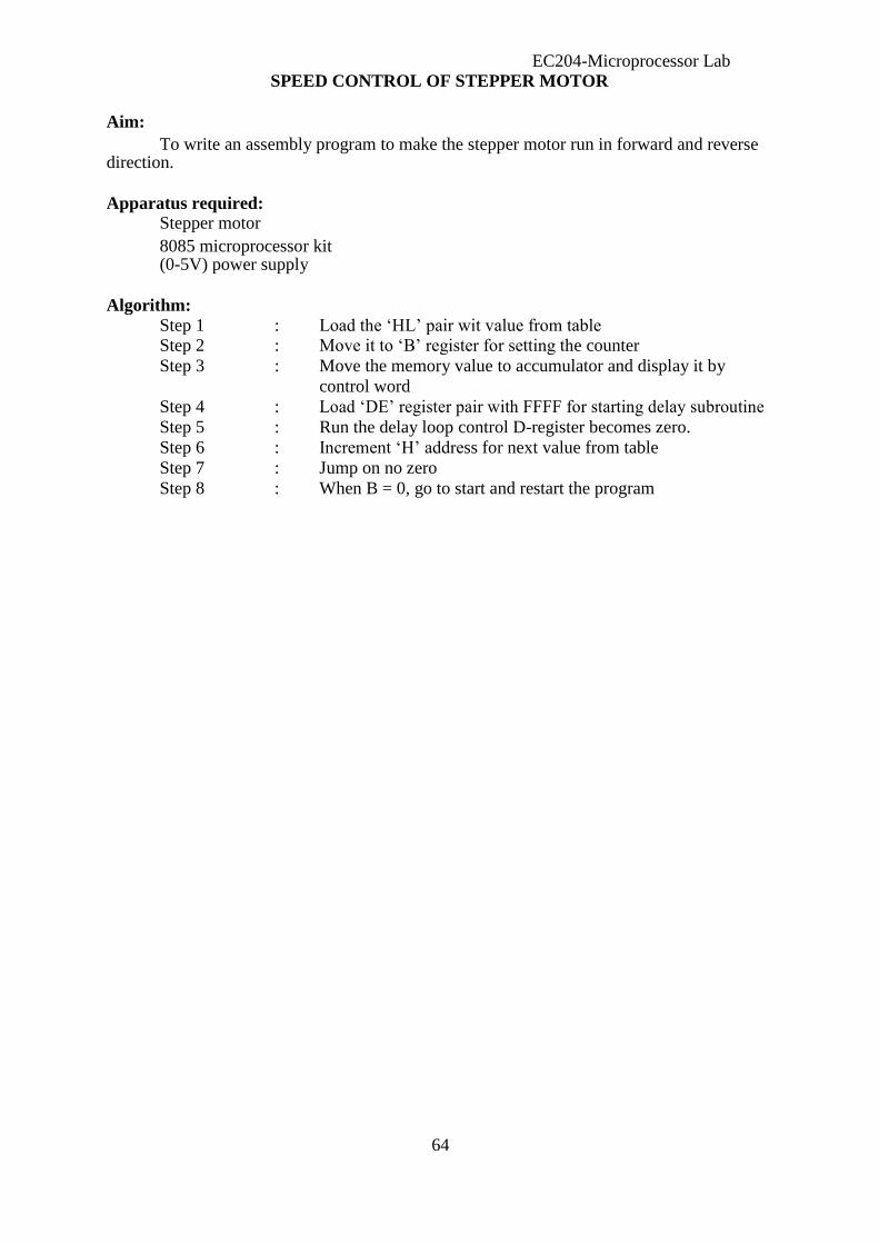
EC204-Microprocessor Lab SPEED CONTROL OF STEPPER MOTOR
Aim: To write an assembly program to make the stepper motor run in forward and reverse
direction.
Apparatus required: Stepper motor 8085 microprocessor kit (0-5V) power supply
Algorithm:
Step 1 : Load the „HL‟ pair wit value from table Step 2 : Move it to „B‟ register for setting the counter
Step 3 : Move the memory value to accumulator and display it by
control word
Step 4 : Load „DE‟ register pair with FFFF for starting delay subroutine
Step 5 : Run the delay loop control D-register becomes zero.
Step 6 : Increment „H‟ address for next value from table
Step 7 : Jump on no zero
Step 8 : When B = 0, go to start and restart the program 64

EC204-Microprocessor Lab
START
Load „HL‟ register pair with data
Load „E‟ with „04‟ (count)
Move memory to accumulator Display the accumulator content (8 bit port)
Load the „DE‟ pair with „FFFF‟
Start delay subroutine
Decrement „D‟ by one, check „OR‟ gate
between „D‟ and E
D = 0 ?
Increment „HL‟ pair by one (count)
Decrement „B‟ count by one
Cy = ?
65

EC204-Microprocessor Lab
Memory Hex Code Label Mnemonics Comments
Location Op code Operand
4100 Start LXI H,Look up 21,1A,41 Load the „HL‟ with
data
4103 MVI B,04 06,04 B = 04
4105 Repeat MOV A,M 7E Memory value to „A‟
4106 OUT C0 D3, C0 Display it
4108 LXI D,03,03 11 Load „DE‟ with FFFF
410B Delay NOP 00 Start delay loop
410C DCX D 1B Decrement DE by 1
410D MOV A,E 7B Move „E‟ to „A‟
410E ORA D B2 Check De = 0 or not
410F JNZ DELAY C2, 0B,41 Jump on zero
4112 INX H 23 Increment HL by 1
4113 DCR B 05 Decrement B by 1
4114 JNZ Repeat C2,05,41 Jump on no zero
4117 JMP START C3,00,41 Jump to start
Input
Input Address Value
411A 0A
411B 06
411C 05
411D 09
Reverse Direction
Output Address Value
411A 09
411B 05
411C 06
411D 0A
Result: Thus, an assembly language program to control of stepper motor was written using
8085 microprocessor kit.
66
EC204-Microprocessor Lab
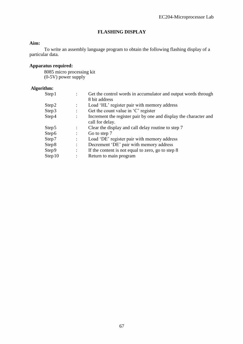
FLASHING DISPLAY
Aim: To write an assembly language program to obtain the following flashing display of a
particular data.
Apparatus required: 8085 micro processing kit (0-5V) power supply
Algorithm:
Step 1 : Get the control words in accumulator and output words through 8 bit address
Step 2 : Load „HL‟ register pair with memory address
Step 3 : Get the count value in „C‟ register
Step 4 : Increment the register pair by one and display the character and
call for delay.
Step 5 : Clear the display and call delay routine to step 7
Step 6 : Go to step 7
Step 7 : Load „DE‟ register pair with memory address
Step 8 : Decrement „DE‟ pair with memory address
Step 9 : If the content is not equal to zero, go to step 8
Step 10 : Return to main program 67

EC204-Microprocessor Lab
START
Load the control loads for flashing display Load the register pair „HL‟ with specified address
Transfer count from memory to „C‟ register
Increment memory address
Transfer memory count in accumulator
Output accumulator content to a data register
Increment count in register „c‟
No Check for
carry?
Yes
Call delay
Load control word for linear screen
Call delay
Load „DE‟ with memory address
No If
Content ?
Yes
Return
68

EC204-Microprocessor Lab
Memory Hex Code Label Mnemonics Comments
Location Op code Operand
4300 MVI A,00 3E,00 Intialise „A‟ as „00‟
4302 OUT 01 DE,01 Out the control word
trough 8 bit
4304 MVI A,90 3E,90 Intialise „a‟ with cw for
RAM
4306 OUT 01 D3,01 Out the cw
4308 MVI A,CC 3E,CC A = CC
430A OUT 01 0D,01 Out the cw
430C Loop 2 LXI H,5000 21,00,50 Load „HL‟ with
430F MOV C,M 4E M to C
4310 Loop 1 INX H 23 Increment „H‟ by
4311 MOV A,M 7E Move M to A
4312 OUT 00 D3, 00 Out the character
4314 DCR C 0D Decrement „C‟ by 1
4315 JNZ Loop 1 C2,10,43 Check for zero
4318 CALL Delay C0,00,46 Call subroutine
431B MVI A,DC 3E,DC A <- 0C
431D OUT 01 D3, 01 A<-01
431F CALL Delay CD,00,46 Call subroutine
4322 JMP Loop 2 C3 0C,43 Check for zf
4600 Delay LXI D,FFFF 11,FF,FF Intialise DE=FFFF
4603 Loop 3 DCX D 1B Decrement DE by 1
4604 MOV A,E 7B Move „E‟ to „A‟
4605 ORA D B2 Check „De‟ = „00‟
4606 JNZ Loop 3 C2,03,46 Jump on no zero
4609 RET C9 C9 Return to main
program
Input
Input Address Value
5000 05
5001 68
5002 68
5003 68
5004 FD
5005 88
Output
EEE – A
Result: Thus, an assembly language program to obtain flashing display of a particular data
was written using 8085 microprocessor kit. 69

EC204-Microprocessor Lab
ROLLING DISPLAY
Aim: To write an assembly language program to obtain a rolling display of a particular data
by using 8085 microprocessor
Apparatus required: 8085 micro processing kit (0-5V) power supply
Algorithm:
Step 1 : Get the control words in accumulator and output the control words through 8 bit port address
Step 2 : Load „HL‟ register pair with memory address and transfer
memory content to „C‟ register
Step 3 : Increment „HL‟ pair with one and transfer the particular bit
pattern through 8 bit port address
Step 4 : Call subroutine delay at step 6
Step 5 : If the count value in „C‟ is not equal to zero then go to step 3
else go to step 2
Step 6 : Load „DE‟ register pair by memory address
Step 7 : Decrement „DE‟ register pair by one
Step 8 : If DE is not equal to zero, go to step 7 else main program 70

EC204-Microprocessor Lab
Delay
Intialise register „D‟ with maximum count „EE‟ Intialise register „c‟ with maximum count „EE‟
Decrement register „C‟ count by one
If No
Reg „C‟
Count ?
Yes
Decrement register „D‟ content by one
No
If reg „D‟
Count ?
Yes
Return
71
EC204-Microprocessor Lab
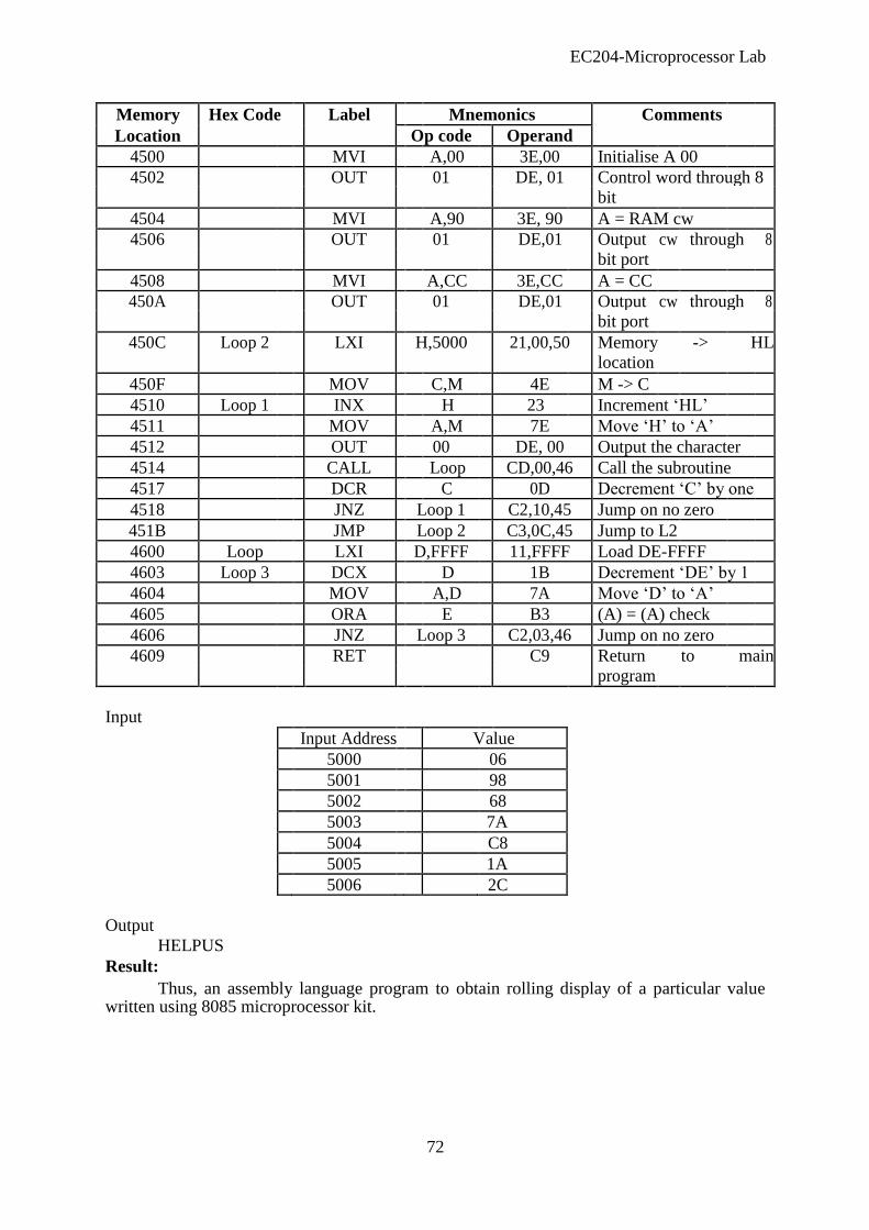
Memory Hex Code Label Mnemonics Comments
Location Op code Operand
4500 MVI A,00 3E,00 Initialise A 00
4502 OUT 01 DE, 01 Control word through 8
bit
4504 MVI A,90 3E, 90 A = RAM cw
4506 OUT 01 DE,01 Output cw through 8
bit port
4508 MVI A,CC 3E,CC A = CC
450A OUT 01 DE,01 Output cw through 8
bit port
450C Loop 2 LXI H,5000 21,00,50 Memory -> HL
location
450F MOV C,M 4E M -> C
4510 Loop 1 INX H 23 Increment „HL‟
4511 MOV A,M 7E Move „H‟ to „A‟
4512 OUT 00 DE, 00 Output the character
4514 CALL Loop CD,00,46 Call the subroutine
4517 DCR C 0D Decrement „C‟ by one
4518 JNZ Loop 1 C2,10,45 Jump on no zero
451B JMP Loop 2 C3,0C,45 Jump to L2
4600 Loop LXI D,FFFF 11,FFFF Load DE-FFFF
4603 Loop 3 DCX D 1B Decrement „DE‟ by 1
4604 MOV A,D 7A Move „D‟ to „A‟
4605 ORA E B3 (A) = (A) check
4606 JNZ Loop 3 C2,03,46 Jump on no zero
4609 RET C9 Return to main
program
Input
Input Address Value
5000 06
5001 98
5002 68
5003 7A
5004 C8
5005 1A
5006 2C
Output
HELPUS Result:
Thus, an assembly language program to obtain rolling display of a particular value written using 8085 microprocessor kit.
72
EC204-Microprocessor Lab
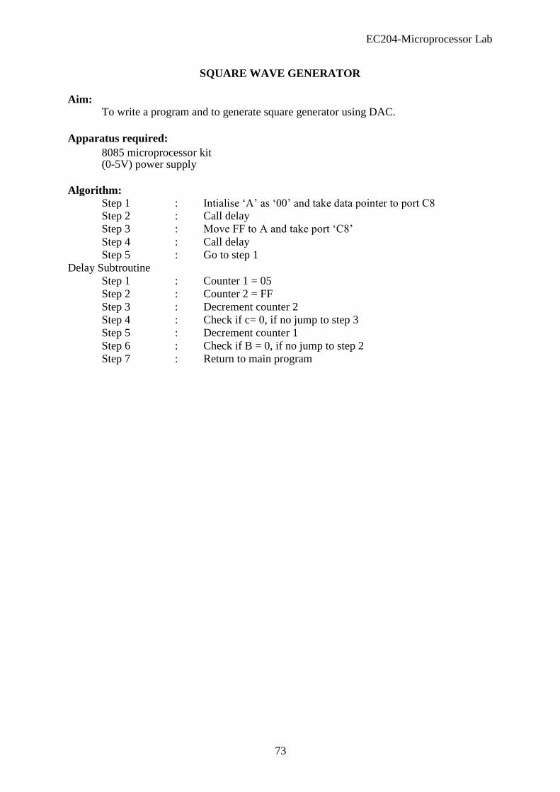
SQUARE WAVE GENERATOR
Aim: To write a program and to generate square generator using DAC.
Apparatus required: 8085 microprocessor kit (0-5V) power supply
Algorithm:
Step 1 : Intialise „A‟ as „00‟ and take data pointer to port C8 Step 2 : Call delay
Step 3 : Move FF to A and take port „C8‟
Step 4 : Call delay
Step 5 : Go to step 1
Delay Subtroutine
Step 1 : Counter 1 = 05
Step 2 : Counter 2 = FF
Step 3 : Decrement counter 2
Step 4 : Check if c= 0, if no jump to step 3
Step 5 : Decrement counter 1
Step 6 : Check if B = 0, if no jump to step 2
Step 7 : Return to main program 73

EC204-Microprocessor Lab
START
Load the control words as for displaying
Call the delay subtroutine program
Intialise the accumulator as „EE‟
Output the accumulator contents register
Call the delay subroutine program
Jump to the start of program
Intialise „B‟ as 05 and „C‟ as „FF‟ and decrement „c‟ by one
Check for
c = ?
No
Yes
Decrement the value of „B‟
No Check for B = 0 ?
Yes
Return
74

EC204-Microprocessor Lab
Memory Hex Code Label Mnemonics Comments
Location Op code Operand
4100 3E,00 Start MVI A,00 Intialise „A‟ with „00‟
4102 D3,C8 OUT C8 Load the control words
4104 CD,11,41 CALL Delay Call delay sutroutine
4107 3E,FF MVI A,FF Intialise „A‟ with „FF
4109 D3,C8 OUT C8 A -> C8
410B CD,11,41 CALL Delay Call delay subroutine
410E C3,00,41 JMP Start Jump to start
4111 06,05 Delay MVI B,05 B -> 05
4113 0E Loop 1 MVI C,FF [C] => FF
4115 OD Loop 2 DCR C Decrement „C‟ register
4116 C2,15,41 JNZ Loop 2 Jump on no zero
4119 05 DCR B Decrement „B‟ register
411A C2,13,41 JNZ Loop 1 Jump on n zero
411D C9 RET Return to main program
Result:
Thus square wave was generated using 8085 microprocessor kit.
75

EC204-Microprocessor Lab
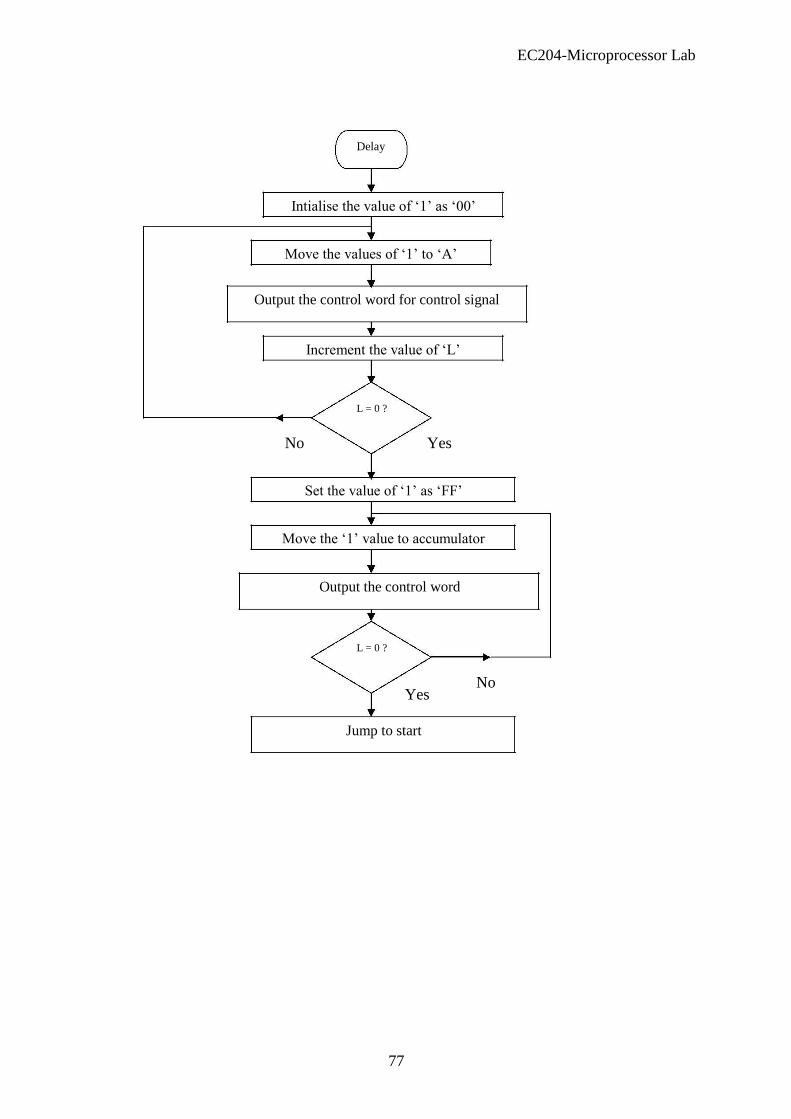
TRIANGULAR WAVE GENERATOR
Aim: To write an assembly language program for generating triangular wave using DAC.
Apparatus required: 8085 micro processor kit (0-5V) DC battery
Algorithm:
Step 1 : Move content of „C‟ to „A‟ where „L‟ is intialised to „00‟ Step 2 : Output content of C8
Step 3 : Increment L till zf = 0
Step 4 : Intialise „L‟ register with FF
Step 5 : Move content of „L‟ to accumulator and output to port
Step 6 : Decrement „L‟ if not equal to zero jump else go to next step
Step 7 : Jump on next step
76
EC204-Microprocessor Lab
Delay
Intialise the value of „1‟ as „00‟
Move the values of „1‟ to „A‟ Output the control word for control signal
Increment the value of „L‟
L = 0 ?
No Yes
Set the value of „1‟ as „FF‟
Move the „1‟ value to accumulator
Output the control word
L = 0 ?
Yes
Jump to start
No
77
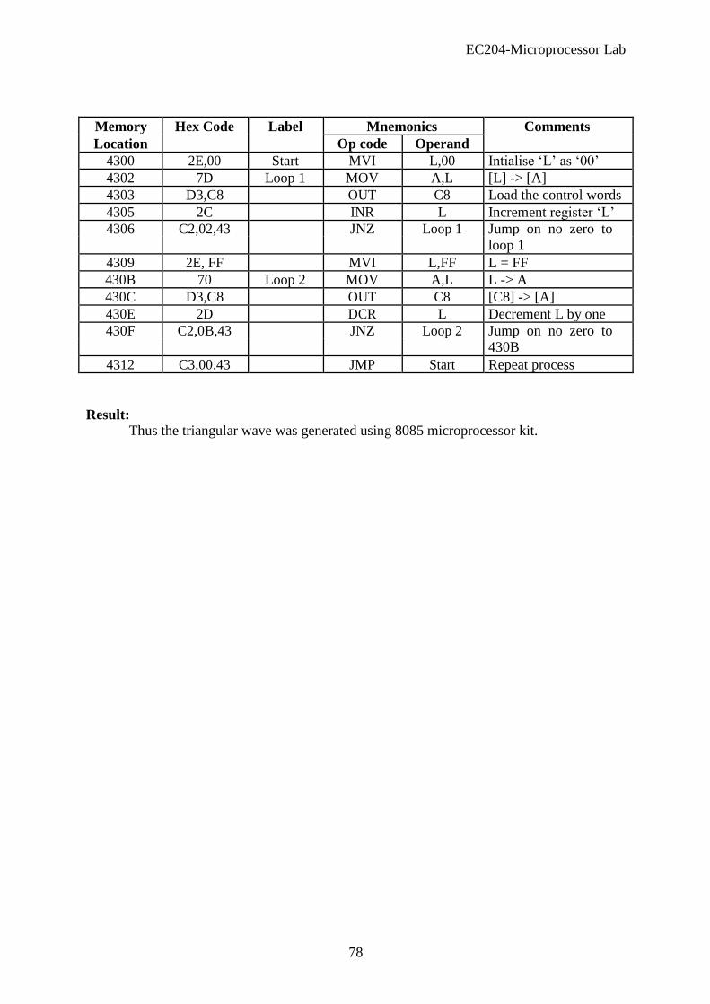
EC204-Microprocessor Lab
Memory Hex Code Label Mnemonics Comments
Location Op code Operand
4300 2E,00 Start MVI L,00 Intialise „L‟ as „00‟
4302 7D Loop 1 MOV A,L [L] -> [A]
4303 D3,C8 OUT C8 Load the control words
4305 2C INR L Increment register „L‟
4306 C2,02,43 JNZ Loop 1 Jump on no zero to loop 1
4309 2E, FF MVI L,FF L = FF
430B 70 Loop 2 MOV A,L L -> A
430C D3,C8 OUT C8 [C8] -> [A]
430E 2D DCR L Decrement L by one
430F C2,0B,43 JNZ Loop 2 Jump on no zero to
430B
4312 C3,00.43 JMP Start Repeat process
Result: Thus the triangular wave was generated using 8085 microprocessor kit.
78
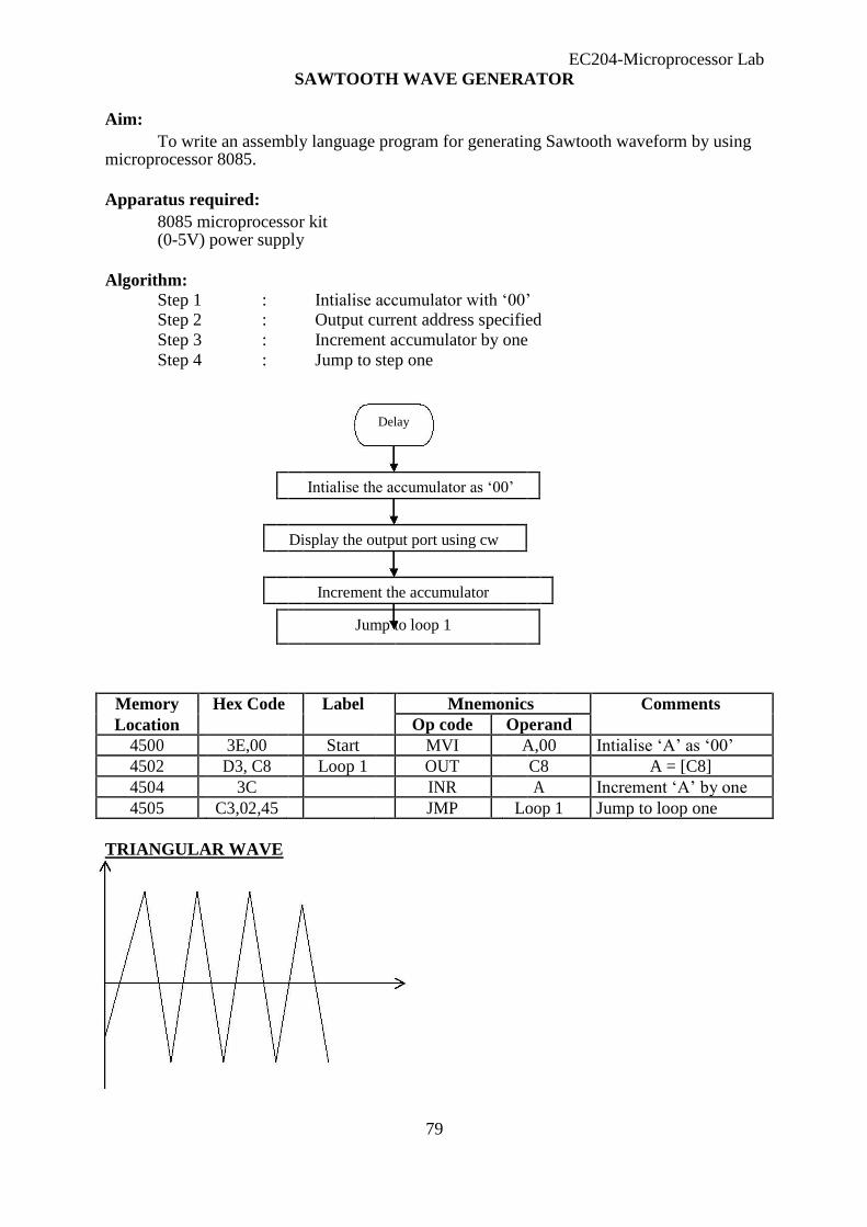
EC204-Microprocessor Lab SAWTOOTH WAVE GENERATOR
Aim: To write an assembly language program for generating Sawtooth waveform by using
microprocessor 8085.
Apparatus required: 8085 microprocessor kit (0-5V) power supply
Algorithm:
Step 1 : Intialise accumulator with „00‟
Step 2 : Output current address specified
Step 3 : Increment accumulator by one
Step 4 : Jump to step one
Delay
Intialise the accumulator as „00‟
Display the output port using cw
Increment the accumulator
Jump to loop 1
Memory Hex Code Label Mnemonics Comments
Location Op code Operand
4500 3E,00 Start MVI A,00 Intialise „A‟ as „00‟
4502 D3, C8 Loop 1 OUT C8 A = [C8]
4504 3C INR A Increment „A‟ by one
4505 C3,02,45 JMP Loop 1 Jump to loop one
TRIANGULAR WAVE
79

EC204-Microprocessor Lab
SAW TOOTH WAVE
SQUARE WAVE
Result: Thus the Sawtooth wave was generated using 8085 microprocessor kit.
80
EC204-Microprocessor Lab
ANALOG TO DIGITAL CONVERTER
Aim: To write an assembly language program to convert analog to digital signal and to
display it in 7 segment LED display
Apparatus required: 8085 microprocessor kit (0-5V) power supply
Algorithm:
Step 1 : Access the channel of ADC Step 2 : Intialise the accumulator with start of conversion signal &
output it to the ADC
Step 3 : Send „0‟ signal for ending the conversion for ADC
Step 4 : Get the analog value converted to display from ADC
Step 5 : The digital signal is separated into two nibbles and displayed in
hexadecimal from by calling service subroutine.
Step 6 : Go to step 1
81
EC204-Microprocessor Lab
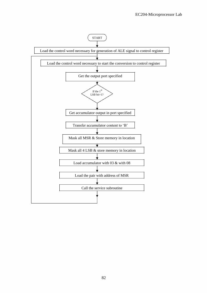
START
Load the control word necessary for generation of ALE signal to control register
Load the control word necessary to start the conversion to control register
Get the output port specified
If the 1st
LSB bit=1?
Get accumulator output in port specified
Transfer accumulator content to „B‟
Mask all MSR & Store memory in location
Mask all 4 LSB & store memory in location
Load accumulator with 03 & with 08
Load the pair with address of MSR
Call the service subroutine
82

EC204-Microprocessor Lab
Memory Hex Code Label Mnemonics Comments
Location Op code Operand
5000 3E,10 MVI A,10 Intialise „a‟ with 10
5002 D3,C OUT C8 Output channel through
5004 3E,18 MVI A,18 Intialise „A‟ with 18
5006 D3, C8 OUT C8 Output channel through
8 bit port
5008 00 NOP No operation
5009 00 NOP No operation
500A 3E,10 MVI A,10 Intialise „A‟ with 2nd
signal
500C D3,C8 OUT C8 Output channel through 8 bit port
500E 3E,01 L2 MVI A,01 Intialise „A‟ with 2nd
5010 D3,D0 OUT D0 Output through 8 bit
5012 00 NOP
5013 00 NOP
5014 00 NOP
5015 3E,00 MVI A,00
5017 D3,D0 OUT D0
5019 DB,D8 L1 IN D8
501B E6,01 ANI 01
501D CA,19,50 JZ L1
5020 DB,C0 IN C0 Get input from
5022 47 MOV B,A B -> A
5023 E6,0F ANI 0F And of with „A‟
5025 32,51,51 STA 5151 Store in 5151
5028 78 MOV A,B B -> A
5029 E6,F0 ANI F0 And F0 with A
502B 0F RRC Rotate content „A‟
502C 0F RRC
502E 0F RRC
502F 32,50,51 STA 550 Store MSB in 5150
5032 3E,03 MVI A,03 03 -> A
5034 0E,08 MVI C,08 08 -> C
5036 21,50,51 LXI H 5150 Load „HL‟ pair with 5150
5039 CD,05,00 CALL 0005 Call device subroutine
503C C3,0E,50 JMP 500E Jump to 500E
Result: Thus the analog to digital conversion was done microprocessor.
83

Microcontroller Lab
ARTHMETIC OPERATIONS USING 8051
Aim: To do the arithmetic operations using 8051 microcontroller
Apparatus required: 8085 microprocessor kit DAC interface kit Keyboard
Algorithm:
Addition / Subtraction Move 1
H data to memory
Step 1 :
Step 2 : Add or subtract 1H
data with 2nd
data
Step 3 : Initialize data pointer.
Step 4 : Move result to memory pointed by DPTR.
START
Out 1H
data in memory
Add or subtract 1H
and 1st
data
Initialize DPTR
Move result to memory preset by DPTR
Stop
84

Microcontroller Lab
Program: 8-bit Addition:
Memory Label Opcode Mnemonics Comments
Location
4100 Start C3 CLR C Clear the carry flat
4101 74DA MOV A, # data 1 Moves data 1 to register A
4103 24DA ADD A, # data 2 Add content of A and data 2 and store in A
4105 464500 MOV DPTR, # 4500 Moves data 4500 to
DPTR
4108 F0 MOV A @ DPTR, A Moves control of A to
location pointed DTPR
4109 80 FE SJMP 4109 Short jump to 4109
Execution:
Addition:
ML Input
4103 0L
4109 03
ML Output
4500 05
Program: 8-bit Subtraction:
Memory Label Opcode Mnemonics Comments
Location
4100 Start C3 CLR C Clear the carry flat
4101 74DA MOV A, # data 1 Moves data 1 to register A
4103 24DA SUB B, # data 2 Subtract data 2 from content of A and store
result in A
4105 464500 MOV DPTR, # 4500 Moves 4500 to DPTR
4108 F0 MOV X @ DPTR, A Moves result by
location by DTPR
4109 80 FE SJMP 4109 Short jump to 4109
Execution:
Subtraction:
ML Input
4101 05
4103 02
ML Output
4500 03
Result:
Thus 8-bit addition, subtraction is performed using 8051.
85

Microcontroller Lab
ARTHMETIC OPERATIONS USING 8051
Aim: To do the arithmetic operations using 8051 microprocessor
Apparatus required: 8085 microprocessor kit DAC interface kit Keyboard
Algorithm:
Multiplication / Division Get 1
H data and 2
nd data to memory
Step 1 :
Step 2 : Multiply or divide 1H
data with 2nd
data
Step 3 : Initialize data pointer.
Step 4 : Move result to memory pointed by DPTR (first port)
Step 5 : Increment DPTR
Step 6 : Move 2nd
part of result to register A
Step 7 : Move result to 2nd
memory location pointer by DPTR
START
Get data into the register
Complement the data
Move the data to pointer by DPTR
Increment data
Increment DPTR
Move data into paste location
Short jump to preset location
Stop
86

Yes
Microcontroller Lab
Program: 8-bit Multiplication:
Memory Label Opcode Mnemonics Comments
Location
4100 Start 7403 MOV A, # data 1 Move immediate data
to accumulator
4101 75F003 MOV B, # data 2 Move 2nd
data to B register
4105 A4 MUL A B Get the product in A &
B
4106 904500 MOV DPTR, # 4500 Load data in 4500
location
4109 F0 MOV X @DPTR, A Move A t ext RAM
410B E5F0 MOV A,B Move 2nd
data in A
410D F0 MOV A @ DPTR Same the ext RAM
410E 80FE SJMP 410E Remain idle in infinite
loop
Execution:
Multiplication: ML Input
4101 0L
4103 04
Program: 8-bit Division:
Output Address Value
4500 08
Memory Label Opcode Mnemonics Comments
Location
4100 Start 7408 MOV A, # data 1 Move immediate data to accumulator
4102 75F002 MOV B, @ data 2 DIV Move immediate to B AB reg.
4105 84 DIV AB Divide content of A &
B
4106 904500 MOV DPTR, # 4500 Load data pointer with
4500 location
4109 F0 MOV X @ DPTR, A Move A to ext RAM
410A A3 INC DPTR Increment data pointer
410B ESF0 MOV A,B Move remainder to A
410D F0 MOV @ DPTR, A Move A to ext RAM
410E 80FE SJMP 410E Remain idle in infinite
loop
Execution:
Division:
ML Input
4101 08
4103 04
Output Address Value
4500 02
Result: Thus 8-bit multiplication & division is performed using 8051.
87