micropower low-voltage, rail-to-rail comparators · this is information on a product in full...
TRANSCRIPT

This is information on a product in full production.
April 2013 DocID17272 Rev 4 1/27
27
TS331, TS332, TS334
Micropower low-voltage, rail-to-rail comparators
Datasheet - production data
Features
• Supply operation from 1.6 V to 5 V
• Low current consumption: 20 μA
• Rail-to-rail inputs
• Wide temperature range: -40 °C to +125 °C
• Low output saturation voltage
• Low propagation delay: 210 ns
• Open-drain output
• ESD tolerance: 2 kV HBM/200 V MM
• SMD packages
• Automotive qualified
Applications
• Mobile phones
• Notebooks and PDAs
• Battery-supplied electronics
• General-purpose portable devices
• General-purpose low voltage applications
Description
The TS331, TS332 and TS334 are single, dual and quad micropower and low-voltage comparators. They can operate with a supply voltage ranging from 1.6 V to 5 V with a typical current consumption as low as 20 μA. In addition, rail-to-rail inputs make them a perfect choice for low-voltage applications.
Their availability in tiny packages is a real advantage for overcoming space constraints.
The TS33x are specified for temperatures between -40 °C to +125 °C, making them ideal for a wide range of applications.
TS331 (single)
TS332 (dual)
TS334 (quad)
SOT23-5/SC70-5 DFN6 1.2x1.3
SO8 MiniSO8
SO14 TSSOP14
DFN8 2x2
QFN16 3x3
www.st.com
Contents TS331, TS332, TS334
2/27 DocID17272 Rev 4
Contents
1 Package pin connections . . . . . . . . . . . . . . . . . . . . . . . . . . . . . . . . . . . . . 3
2 Absolute maximum ratings and operating conditions . . . . . . . . . . . . . 4
3 Electrical characteristics . . . . . . . . . . . . . . . . . . . . . . . . . . . . . . . . . . . . . 6
4 Package information . . . . . . . . . . . . . . . . . . . . . . . . . . . . . . . . . . . . . . . . 13
4.1 SOT23-5 package information . . . . . . . . . . . . . . . . . . . . . . . . . . . . . . . . . 14
4.2 SC70-5 (SOT323-5) package information . . . . . . . . . . . . . . . . . . . . . . . . 15
4.3 DFN6 1.2x1.3 package information . . . . . . . . . . . . . . . . . . . . . . . . . . . . . 16
4.4 DFN8 2x2 package information . . . . . . . . . . . . . . . . . . . . . . . . . . . . . . . . 17
4.5 SO8 package information . . . . . . . . . . . . . . . . . . . . . . . . . . . . . . . . . . . . . 19
4.6 MiniSO8 package information . . . . . . . . . . . . . . . . . . . . . . . . . . . . . . . . . 20
4.7 QFN16 3x3 package information . . . . . . . . . . . . . . . . . . . . . . . . . . . . . . . 21
4.8 SO14 package information . . . . . . . . . . . . . . . . . . . . . . . . . . . . . . . . . . . . 23
4.9 TSSOP14 package information . . . . . . . . . . . . . . . . . . . . . . . . . . . . . . . . 24
5 Ordering information . . . . . . . . . . . . . . . . . . . . . . . . . . . . . . . . . . . . . . . 25
6 Revision history . . . . . . . . . . . . . . . . . . . . . . . . . . . . . . . . . . . . . . . . . . . 26

DocID17272 Rev 4 3/27
TS331, TS332, TS334 Package pin connections
1 Package pin connections
Figure 1. Pin connections for each package (top view)
1. NC = not connected
2. The exposed pads of the DFN8 2x2 and the QFN16 3x3 can be connected to VCC- or left floating.
TS332
TS331
TS334
SOT23-5/SC70-5
SO8/MiniSO8
SO14/TSSOP14
TS331DFN6 1.2x1.3
14
13
12
11
10
9
87
6
5
4
3
2
1OUT2
VCC+
OUT1
IN1-
IN1+
IN2-
IN2+
OUT3
VCC-
OUT4
IN4+
IN4-
IN3+
IN3-
TS334QFN16 3x3
TS332DFN8 2x2

Absolute maximum ratings and operating conditions TS331, TS332, TS334
4/27 DocID17272 Rev 4
2 Absolute maximum ratings and operating conditions
Table 1. Absolute maximum ratings
Symbol Parameter Value Unit
VCC Supply voltage(1)
1. All voltage values, except differential voltage, are referenced to Vcc-
5.5
VVID Differential input voltage ± 5.5
VIN Input voltage range (VCC-) - 0.3 to (VCC+) + 0.3
Vout Output voltage(1) 5.5
Rthja
Thermal resistance junction to ambient(2)
SOT23-5 SC70-5 DFN6 1.2x1.3 DFN8 2x2 SO8 MiniSO8 QFN16 3x3 SO14 TSSOP14
2. Short-circuits can cause excessive heating. These values are typical
2502054057
12519039
105100 °C/W
Rthjc
Thermal resistance junction to case (2)
SOT23-5 SC70-5 SO8 MiniSO8 QFN16 3x3 SO14 TSSOP14
8117240395
3132
Tstg Storage temperature -65 to +150
°CTj Junction temperature 150
TLEAD Lead temperature (soldering 10 seconds) 260
ESD
Human body model (HBM)(3)
3. According to JEDEC standard JESD22-A114F.
2000
VMachine model (MM)(4)
4. According to JEDEC standard JESD22-A115A.
200
Charged device model (CDM)(5)
5. According to ANSI/ESD STM5.3.1.
1500
Latchup immunity 200 mA

DocID17272 Rev 4 5/27
TS331, TS332, TS334 Absolute maximum ratings and operating conditions
Table 2. Operating conditions
Symbol Parameter Value Unit
Toper Operating temperature range -40 to +125 °C
VCCSupply voltage (VCC+) - (VCC-) -40°C < Tamb < +125°C 1.6 to 5.0
V
VICM
Common mode input voltage range Tamb = +25°C -40°C < Tamb < +125°C
(VCC-) - 0.2 to (VCC+) + 0.2(VCC-) to (VCC+)

Electrical characteristics TS331, TS332, TS334
6/27 DocID17272 Rev 4
3 Electrical characteristics
Table 3. VCC+ = +1.8 V, VCC- = 0 V, Tamb = +25°C (unless otherwise specified)
Symbol Parameter Test conditions Min. Typ. Max. Unit
VIO Input offset voltage0.5 5
mV-40 °C < Tamb < +125 °C 6
ΔVio/ΔT Input offset voltage drift -40 °C < Tamb < +125 °C 4.5 μV/°C
IIB Input bias current(1)25 40
nA-40°C < Tamb < +125 °C 100
IIO Input offset current(1)1 10
-40°C < Tamb < +125 °C 100
ICC Supply current
No load, output low, VICM = 0 V 20 26
μA-40 °C < Tamb < +125 °C 30
No load, output high, VICM = 0 V 22 29
-40 °C < Tamb < +125 °C 33
IOH Output current leakageVOUT = VCC+ 1 10
nA-40 °C < Tamb < +125 °C 500
VOL Output voltage lowISINK = 1 mA 24 30
mV-40 °C < Tamb < +125 °C 50
ISINK Output sink currentVOUT = 1.5 V 20 22
mA-40°C < Tamb < +125°C 15
CMRR Common mode rejection ratio 0 < VICM < 1.8 V 50 68 dB
TPHLPropagation delay(2) High to low output level
VICM = 0 V, RL = 5.1 kΩ, CL = 50 pF, overdrive = 10 mV
300
ns
VICM = 0 V, RL = 5.1 kΩ, CL = 50 pF, overdrive = 100 mV
210 310
TPLHPropagation delay(3) Low to high output level
VICM = 0 V, RL = 5.1 kΩ, CL = 50 pF, overdrive = 10 mV
540
VICM = 0 V, RL = 5.1 kΩ, CL = 50 pF, overdrive = 100 mV
420 620
1. Maximum values include unavoidable inaccuracies of the industrial tests.
2. TPHL is measured when the output signal crosses a voltage level at 50% of Vcc with the following conditions: inverting input voltage (IN-) = VICM and non-inverting input voltage (IN+) moving from VICM + 100 mV to VICM - overdrive.
3. TPLH is measured when the output signal crosses a voltage level at 50% of Vcc with the following conditions: inverting input voltage (IN-) = VICM and non-inverting input voltage (IN+) moving from VICM - 100 mV to VICM + overdrive.

DocID17272 Rev 4 7/27
TS331, TS332, TS334 Electrical characteristics
Table 4. VCC+ = +2.7 V, VCC- = 0 V, Tamb = +25°C (unless otherwise specified)
Symbol Parameter Test conditions Min. Typ. Max. Unit
VIO Input offset voltage0.5 5
mV-40 °C < Tamb < +125 °C 6
ΔVio/ΔT Input offset voltage drift -40 °C < Tamb < +125 °C 3.3 μV/°C
IIB Input bias current(1)25 40
nA-40 °C < Tamb < +125 °C 100
IIO Input offset current(1)1 10
-40 °C < Tamb < +125 °C 100
ICC Supply current
No load, output low, VICM = 0 V 21 27
μA-40 °C < Tamb < +125 °C 31
No load, output high, VICM = 0 V 23 30
-40°C < Tamb < +125 °C 34
IOH Output current leakageVOUT = VCC+ 1 10
nA-40 °C < Tamb < +125 °C 500
VOL Output voltage lowISINK = 1 mA 17 30
mV-40 °C < Tamb < +125 °C 50
ISINK Output sink currentVOUT = 1.5 V 40 47
mA-40 °C < Tamb < +125 °C 30
CMRR Common mode rejection ratio0 < VICM < 2.7 V 54 74 dB
-40 °C < Tamb < +125 °C 53
TPHLPropagation delay(2) High to low output level
VICM = 0 V, RL = 5.1 kΩ, CL = 50 pF, overdrive = 10 mV
320
ns
VICM = 0 V, RL = 5.1 kΩ, CL = 50 pF, overdrive = 100 mV
220 320
TPLHPropagation delay(3) Low to high output level
VICM = 0 V, RL = 5.1 kΩ, CL = 50 pF, overdrive = 10 mV
550
VICM = 0 V, RL = 5.1 kΩ, CL = 50 pF, overdrive = 100 mV
420 640
1. Maximum values include unavoidable inaccuracies of the industrial tests.
2. TPHL is measured when the output signal crosses a voltage level at 50% of Vcc with the following conditions: Inverting input voltage (IN-) = VICM and non-inverting input voltage (IN+) moving from VICM + 100 mV to VICM - overdrive.
3. TPLH is measured when the output signal crosses a voltage level at 50% of Vcc with the following conditions: Inverting input voltage (IN-) = VICM and non-inverting input voltage (IN+) moving from VICM - 100 mV to VICM + overdrive.

Electrical characteristics TS331, TS332, TS334
8/27 DocID17272 Rev 4
Table 5. VCC+ = +5 V, VCC- = 0 V, Tamb = +25°C (unless otherwise specified)
Symbol Parameter Test conditions Min. Typ. Max. Unit
VIO Input offset voltage0.5 5
mV-40 °C < Tamb < +125 °C 6
ΔVio/ΔT Input offset voltage drift -40 °C < Tamb < +125 °C 1.3 μV/°C
IIB Input bias current(1)30 40
nA-40 °C < Tamb < +125 °C 100
IIO Input offset current(1)1 10
-40 °C < Tamb < +125 °C 100
ICC Supply current
No load, output low, VICM = 0 V 23 30
μA-40 °C < Tamb < +125 °C 34
No load, output high, VICM = 0 V 26 34
-40 °C < Tamb < +125 °C 38
IOH Output current leakageVOUT = VCC+ 1 10
nA-40 °C < Tamb < +125 °C 600
VOL Output voltage lowISINK = 4 mA 48 60
mV-40 °C < Tamb < +125 °C 80
ISINK Output sink currentVOUT = 1.5 V 82 93
mA-40 °C < Tamb < +125 °C 60
AV Voltage gain 40 100 V/mV
CMRR Common mode rejection ratio0 < VICM < 5 V 60 79
dB-40 °C < Tamb < +125 °C 58
SVR Supply voltage rejectionΔVCC = 1.8 to 5 V 56 75
-40 °C < Tamb < +125 °C 56
TPHLPropagation delay(2) High to low output level
VICM = 0 V, RL = 5.1 kΩ, CL = 50 pF, overdrive = 10 mV
380
ns
VICM = 0 V, RL = 5.1 kΩ, CL = 50 pF, overdrive = 100 mV
270 430
TPLHPropagation delay(3) Low to high output level
VICM = 0 V, RL = 5.1 kΩ, CL = 50 pF, overdrive = 10 mV
570
VICM = 0 V, RL = 5.1 kΩ, CL = 50 pF, overdrive = 100 mV
450 720
1. Maximum values include unavoidable inaccuracies of the industrial tests.
2. TPHL is measured when the output signal crosses a voltage level at 50% of Vcc with the following conditions: Inverting input voltage (IN-) = VICM and non-inverting input voltage (IN+) moving from VICM + 100 mV to VICM - overdrive.
3. TPLH is measured when the output signal crosses a voltage level at 50% of Vcc with the following conditions: Inverting input voltage (IN-) = VICM and non-inverting input voltage (IN+) moving from VICM - 100 mV to VICM + overdrive.

DocID17272 Rev 4 9/27
TS331, TS332, TS334 Electrical characteristics
Figure 2. Supply current versus supply voltage with output high, VICM = 0 V
Figure 3. Supply current versus supply voltage with output high, VICM = VCC
Figure 4. Supply current versus supply voltage with output low, VICM = 0 V
Figure 5. Supply current versus supply voltage with output low, VICM = VCC
Figure 6. Supply current versus temperature Figure 7. Input bias current versus input common-mode voltage

Electrical characteristics TS331, TS332, TS334
10/27 DocID17272 Rev 4
Figure 8. Input current versus differential input voltage
Figure 9. Input offset voltage versus temperature
Figure 10. Output voltage versus output sink current, VCC = 1.8 V
Figure 11. Output voltage versus output sink current, VCC = 2.7 V
Figure 12. Output voltage versus output sink current, VCC = 5 V
Figure 13. Output sink current versus output voltage
DocID17272 Rev 4 11/27
TS331, TS332, TS334 Electrical characteristics
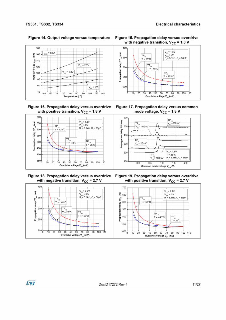
Figure 14. Output voltage versus temperature Figure 15. Propagation delay versus overdrive with negative transition, VCC = 1.8 V
Figure 16. Propagation delay versus overdrive with positive transition, VCC = 1.8 V
Figure 17. Propagation delay versus common mode voltage, VCC = 1.8 V
Figure 18. Propagation delay versus overdrive with negative transition, VCC = 2.7 V
Figure 19. Propagation delay versus overdrive with positive transition, VCC = 2.7 V

Electrical characteristics TS331, TS332, TS334
12/27 DocID17272 Rev 4
Figure 20. Propagation delay versus common mode voltage, VCC = 2.7 V
Figure 21. Propagation delay versus overdrive with negative transition, VCC = 5 V
Figure 22. Propagation delay versus overdrive with positive transition, VCC = 5 V
Figure 23. Propagation delay versus common mode voltage, VCC = 5 V
Figure 24. Propagation delay versus time with negative transition
Figure 25. Propagation delay versus time with positive transition

DocID17272 Rev 4 13/27
TS331, TS332, TS334 Package information
4 Package information
In order to meet environmental requirements, ST offers these devices in different grades of ECOPACK® packages, depending on their level of environmental compliance. ECOPACK® specifications, grade definitions and product status are available at: www.st.com. ECOPACK® is an ST trademark.

Package information TS331, TS332, TS334
14/27 DocID17272 Rev 4
4.1 SOT23-5 package information
Figure 26. SOT23-5 package mechanical drawing
Table 6. SOT23-5 package mechanical data
Ref.
Dimensions
Millimeters Inches(1)
1. Values in inches are rounded to three decimal digits.
Min. Typ. Max. Min. Typ. Max.
A 0.90 1.20 1.45 0.035 0.047 0.057
A1 0.15 0.006
A2 0.90 1.05 1.30 0.035 0.041 0.051
B 0.35 0.40 0.50 0.013 0.015 0.019
C 0.09 0.15 0.20 0.003 0.006 0.008
D 2.80 2.90 3.00 0.110 0.114 0.118
D1 1.90 0.075
e 0.95 0.037
E 2.60 2.80 3.00 0.102 0.110 0.118
F 1.50 1.60 1.75 0.059 0.063 0.069
L 0.10 0.35 0.60 0.004 0.013 0.023
K 0° 10° 0° 10°

DocID17272 Rev 4 15/27
TS331, TS332, TS334 Package information
4.2 SC70-5 (SOT323-5) package information
Figure 27. SC70-5 (SOT323-5) package mechanical drawing
Table 7. SC70-5 (or SOT323-5) package mechanical data
Ref
Dimensions
Millimeters Inches(1)
1. Values in inches are rounded to three decimal digits.
Min Typ Max Min Typ Max
A 0.80 1.10 0.315 0.043
A1 0.10 0.004
A2 0.80 0.90 1.00 0.315 0.035 0.039
b 0.15 0.30 0.006 0.012
c 0.10 0.22 0.004 0.009
D 1.80 2.00 2.20 0.071 0.079 0.087
E 1.80 2.10 2.40 0.071 0.083 0.094
E1 1.15 1.25 1.35 0.045 0.049 0.053
e 0.65 0.025
e1 1.30 0.051
L 0.26 0.36 0.46 0.010 0.014 0.018
< 0° 8° 0° 8°
SEATING PLANE
GAUGE PLANE
DIMENSIONS IN MM
SIDE VIEW
TOP VIEW
COPLANAR LEADS

Package information TS331, TS332, TS334
16/27 DocID17272 Rev 4
4.3 DFN6 1.2x1.3 package information
Figure 28. DFN6 1.2x1.3 package mechanical drawing
Table 8. DFN6 1.2x1.3 package mechanical data
Ref
Dimensions
Millimeters Inches(1)
1. Values in inches are rounded to three decimal digits.
Min Typ Max Min Typ Max
A 0.45 0.50 0.55 0.018 0.020 0.022
A1 0.00 0.02 0.05 0.000 0.001 0.002
b 0.15 0.18 0.25 0.006 0.007 0.002
c 0.05 0.002
D 1.20 0.047
E 1.30 0.051
e 0.4 0.016
L 0.475 0.525 0.575 0.019 0.021 0.023
L3 0.375 0.425 0.475 0.015 0.017 0.019

DocID17272 Rev 4 17/27
TS331, TS332, TS334 Package information
4.4 DFN8 2x2 package information
Figure 29. DFN8 2x2 package mechanical drawing
Table 9. DFN8 2x2x0.6 mm package mechanical data (pitch 0.5 mm)
Ref.
Dimensions
Millimeters Inches
Min. Typ. Max. Min. Typ. Max.
A 0.51 0.55 0.60 0.020 0.022 0.024
A1 0.05 0.002
A3 0.15 0.006
b 0.18 0.25 0.30 0.007 0.010 0.012
D 1.85 2.00 2.15 0.073 0.079 0.085
D2 1.45 1.60 1.70 0.057 0.063 0.067
E 1.85 2.00 2.15 0.073 0.079 0.085
E2 0.75 0.90 1.00 0.030 0.035 0.039
e 0.50 0.020
L 0.425 0.017
ddd 0.08 0.003

Package information TS331, TS332, TS334
18/27 DocID17272 Rev 4
Figure 30. DFN8 2x2 footprint recommendation

DocID17272 Rev 4 19/27
TS331, TS332, TS334 Package information
4.5 SO8 package information
Figure 31. SO8 package mechanical drawing
Table 10. SO8 package mechanical data
Ref.
Dimensions
Millimeters Inches(1)
1. Values in inches are rounded to three decimal digits.
Min. Typ. Max. Min. Typ. Max.
A 1.75 0.069
A1 0.10 0.25 0.004 0.010
A2 1.25 0.049
b 0.28 0.48 0.011 0.019
c 0.17 0.23 0.007 0.010
D 4.80 4.90 5.00 0.189 0.193 0.197
E 5.80 6.00 6.20 0.228 0.236 0.244
E1 3.80 3.90 4.00 0.150 0.154 0.157
e 1.27 0.050
h 0.25 0.50 0.010 0.020
L 0.40 1.27 0.016 0.050
L1 1.04 0.040
k 0 8° 1° 8°
ccc 0.10 0.004

Package information TS331, TS332, TS334
20/27 DocID17272 Rev 4
4.6 MiniSO8 package information
Figure 32. MiniSO8 package mechanical drawing
Table 11. MiniSO8 package mechanical data
Ref.
Dimensions
Millimeters Inches(1)
1. Values in inches are rounded to three decimal digits.
Min. Typ. Max. Min. Typ. Max.
A 1.1 0.043
A1 0 0.15 0 0.006
A2 0.75 0.85 0.95 0.030 0.033 0.037
b 0.22 0.40 0.009 0.016
c 0.08 0.23 0.003 0.009
D 2.80 3.00 3.20 0.11 0.118 0.126
E 4.65 4.90 5.15 0.183 0.193 0.203
E1 2.80 3.00 3.10 0.11 0.118 0.122
e 0.65 0.026
L 0.40 0.60 0.80 0.016 0.024 0.031
L1 0.95 0.037
L2 0.25 0.010
k 0° 8° 0° 8°
ccc 0.10 0.004
DocID17272 Rev 4 21/27
TS331, TS332, TS334 Package information
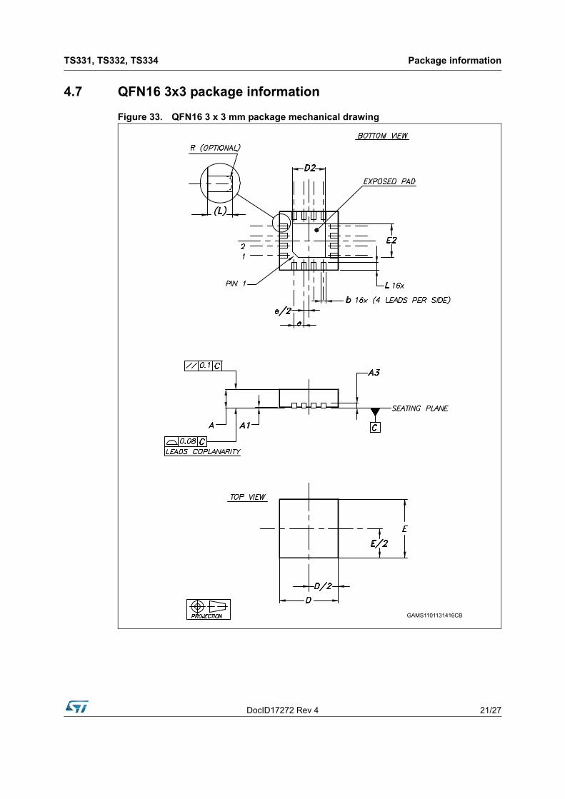
4.7 QFN16 3x3 package information
Figure 33. QFN16 3 x 3 mm package mechanical drawing

Package information TS331, TS332, TS334
22/27 DocID17272 Rev 4
Figure 34. QFN16 3 x 3 mm footprint recommendation
Table 12. QFN16 3 x 3 mm package mechanical data (pitch 0.5 mm)
Ref.
Dimensions
Millimeters Inches
Min. Typ. Max. Min. Typ. Max.
A 0.80 0.90 1.00 0.031 0.035 0.039
A1 0 0.05 0 0.002
A3 0.20 0.008
b 0.18 0.30 0.007 0.012
D 2.90 3.00 3.10 0.114 0.118 0.122
D2 1.50 1.80 0.059 0.071
E 2.90 3.00 3.10 0.114 0.118 0.122
E2 1.50 1.80 0.059 0.071
e 0.50 0.020
L 0.30 0.50 0.012 0.020
DocID17272 Rev 4 23/27
TS331, TS332, TS334 Package information
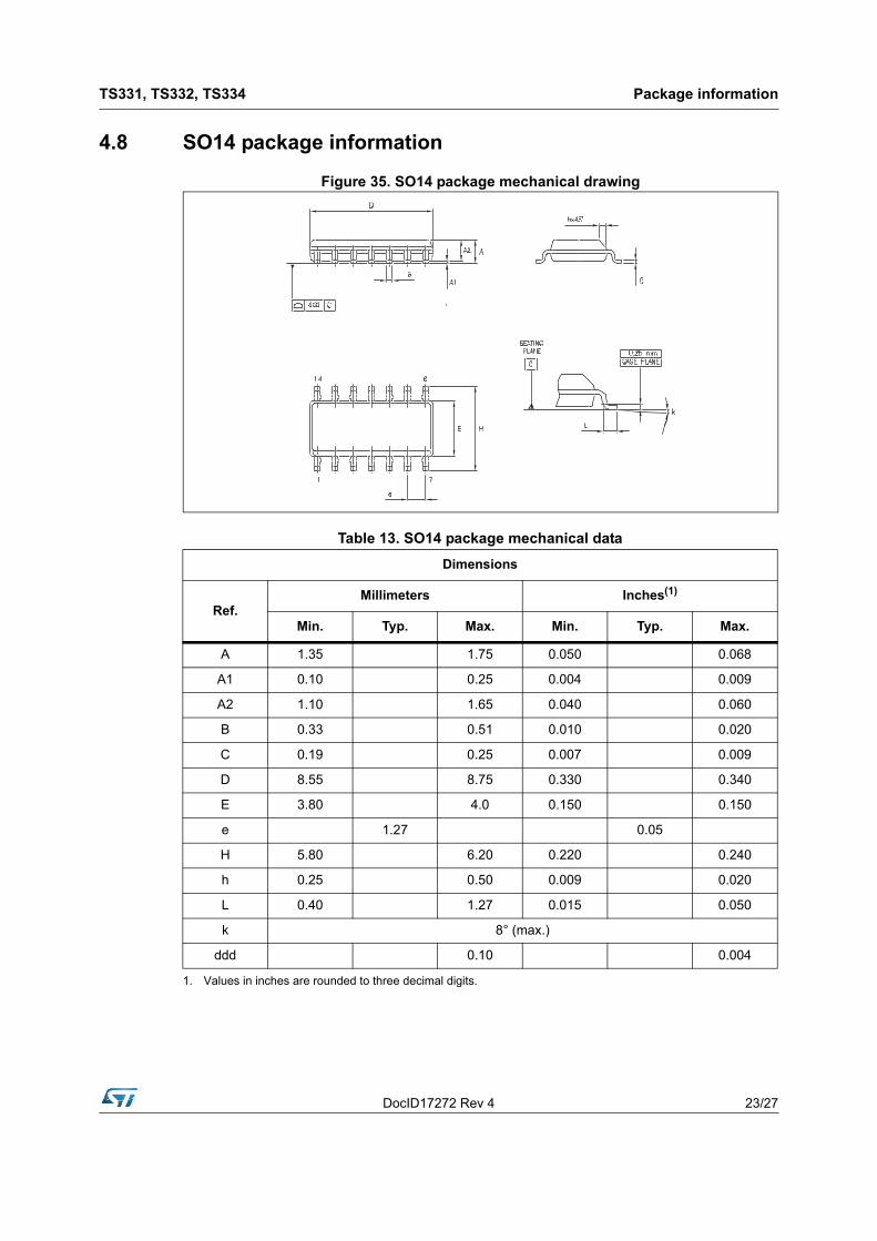
4.8 SO14 package information
Figure 35. SO14 package mechanical drawing
Table 13. SO14 package mechanical data
Dimensions
Ref.Millimeters Inches(1)
1. Values in inches are rounded to three decimal digits.
Min. Typ. Max. Min. Typ. Max.
A 1.35 1.75 0.050 0.068
A1 0.10 0.25 0.004 0.009
A2 1.10 1.65 0.040 0.060
B 0.33 0.51 0.010 0.020
C 0.19 0.25 0.007 0.009
D 8.55 8.75 0.330 0.340
E 3.80 4.0 0.150 0.150
e 1.27 0.05
H 5.80 6.20 0.220 0.240
h 0.25 0.50 0.009 0.020
L 0.40 1.27 0.015 0.050
k 8° (max.)
ddd 0.10 0.004

Package information TS331, TS332, TS334
24/27 DocID17272 Rev 4
4.9 TSSOP14 package information
Figure 36. TSSOP14 package mechanical drawing
Table 14. TSSOP14 package mechanical data
Ref.
Dimensions
Millimeters Inches(1)
1. Values in inches are rounded to three decimal digits.
Min. Typ. Max. Min. Typ. Max.
A 1.20 0.047
A1 0.05 0.15 0.002 0.004 0.006
A2 0.80 1.00 1.05 0.031 0.039 0.041
b 0.19 0.30 0.007 0.012
c 0.09 0.20 0.004 0.0089
D 4.90 5.00 5.10 0.193 0.197 0.201
E 6.20 6.40 6.60 0.244 0.252 0.260
E1 4.30 4.40 4.50 0.169 0.173 0.176
e 0.65 0.0256
L 0.45 0.60 0.75 0.018 0.024 0.030
L1 1.00 0.039
k 0° 8° 0° 8°
aaa 0.10 0.004

DocID17272 Rev 4 25/27
TS331, TS332, TS334 Ordering information
5 Ordering information
Table 15. Order codes
Order code Temperature range Package Packaging Marking
TS331ILT
-40 °C, +125 °C
SOT23-5
Tape and reel
K506
TS331IYLT(1)
1. Qualified and characterized according to AEC Q100 and Q003 or equivalent, advanced screening according to AEC Q001 and Q 002 or equivalent.
K513
TS331ICT SC70-5 K55
TS331IQT DFN6 1.2x1.3 K3
TS332IQ2T DFN8 2x2 K55
TS332IDTSO8
332I
TS332IYDT(1) 332IY
TS332IST MiniSO8 K507
TS334IQ4T QFN16 3x3 K307
TS334IDTSO14
334I
TS334IYDT(1) 334IY
TS334IPTTSSOP14
334I
TS334IYPT(1) 334IY

Revision history TS331, TS332, TS334
26/27 DocID17272 Rev 4
6 Revision history
Table 16. Document revision history
Date Revision Changes
29-Mar-2010 1 Initial release.
01-Dec-2011 2
– Added TS332 and TS334 devices.
– Added Vout parameter in Table 1: Absolute maximum ratings.
– Removed note "The magnitude of input and output voltages must never exceed the supply rail ±0.3 V." from Table 1.
– Removed note "All values over the temperature range are guaranteed through correlation and simulation. No production tests have been performed at the temperature range limits." from Table 3, Table 4 and Table 5.
– Removed "Vicm = 0 V" from Test conditions column in Table 3, Table 4 and Table 5.
– Modified minimal Isink value in Table 5.
29-Oct-2012 3
– Added DFN6 package for TS331
– Modified notes 3, 4, and 5 in Table 1
– Added Automotive grade order codes in Table 15
30-Apr-2013 4
– Added DFN8 2x2 and QFN16 3x3 silhouette, pinout, and package information.
– Figure 1: updated pinout diagrams; added footnote 2.
– Table 1: updated Rthjc and Rthjc
– Table 3, Table 4, Table 5: updated symbol for input offset voltage drift.
– Table 15: added order codes TS332IQ2T, TS334IQ4T, and TS334IYDT.

DocID17272 Rev 4 27/27
TS331, TS332, TS334
Please Read Carefully:
Information in this document is provided solely in connection with ST products. STMicroelectronics NV and its subsidiaries (“ST”) reserve the right to make changes, corrections, modifications or improvements, to this document, and the products and services described herein at any time, without notice.
All ST products are sold pursuant to ST’s terms and conditions of sale.
Purchasers are solely responsible for the choice, selection and use of the ST products and services described herein, and ST assumes no liability whatsoever relating to the choice, selection or use of the ST products and services described herein.
No license, express or implied, by estoppel or otherwise, to any intellectual property rights is granted under this document. If any part of this document refers to any third party products or services it shall not be deemed a license grant by ST for the use of such third party products or services, or any intellectual property contained therein or considered as a warranty covering the use in any manner whatsoever of such third party products or services or any intellectual property contained therein.
UNLESS OTHERWISE SET FORTH IN ST’S TERMS AND CONDITIONS OF SALE ST DISCLAIMS ANY EXPRESS OR IMPLIED WARRANTY WITH RESPECT TO THE USE AND/OR SALE OF ST PRODUCTS INCLUDING WITHOUT LIMITATION IMPLIED WARRANTIES OF MERCHANTABILITY, FITNESS FOR A PARTICULAR PURPOSE (AND THEIR EQUIVALENTS UNDER THE LAWS OF ANY JURISDICTION), OR INFRINGEMENT OF ANY PATENT, COPYRIGHT OR OTHER INTELLECTUAL PROPERTY RIGHT.
ST PRODUCTS ARE NOT AUTHORIZED FOR USE IN WEAPONS. NOR ARE ST PRODUCTS DESIGNED OR AUTHORIZED FOR USE IN: (A) SAFETY CRITICAL APPLICATIONS SUCH AS LIFE SUPPORTING, ACTIVE IMPLANTED DEVICES OR SYSTEMS WITH PRODUCT FUNCTIONAL SAFETY REQUIREMENTS; (B) AERONAUTIC APPLICATIONS; (C) AUTOMOTIVE APPLICATIONS OR ENVIRONMENTS, AND/OR (D) AEROSPACE APPLICATIONS OR ENVIRONMENTS. WHERE ST PRODUCTS ARE NOT DESIGNED FOR SUCH USE, THE PURCHASER SHALL USE PRODUCTS AT PURCHASER’S SOLE RISK, EVEN IF ST HAS BEEN INFORMED IN WRITING OF SUCH USAGE, UNLESS A PRODUCT IS EXPRESSLY DESIGNATED BY ST AS BEING INTENDED FOR “AUTOMOTIVE, AUTOMOTIVE SAFETY OR MEDICAL” INDUSTRY DOMAINS ACCORDING TO ST PRODUCT DESIGN SPECIFICATIONS. PRODUCTS FORMALLY ESCC, QML OR JAN QUALIFIED ARE DEEMED SUITABLE FOR USE IN AEROSPACE BY THE CORRESPONDING GOVERNMENTAL AGENCY.
Resale of ST products with provisions different from the statements and/or technical features set forth in this document shall immediately void any warranty granted by ST for the ST product or service described herein and shall not create or extend in any manner whatsoever, any liability of ST.
ST and the ST logo are trademarks or registered trademarks of ST in various countries.Information in this document supersedes and replaces all information previously supplied.
The ST logo is a registered trademark of STMicroelectronics. All other names are the property of their respective owners.
© 2013 STMicroelectronics - All rights reserved
STMicroelectronics group of companies
Australia - Belgium - Brazil - Canada - China - Czech Republic - Finland - France - Germany - Hong Kong - India - Israel - Italy - Japan - Malaysia - Malta - Morocco - Philippines - Singapore - Spain - Sweden - Switzerland - United Kingdom - United States of America
www.st.com