micropatterning and casting pedot-pss /dmso …charlot/pres/pedot.pdfmicropatterning and casting...
TRANSCRIPT
Micropatterning and casting PEDOT-PSS /DMSO layers
Benoît Charlot, Gilbert Sassine, Alexandra Garraud, Alain Giani, Philippe Combette
IES Institut d’Electronique du Sud CNRS Université Montpellier II Place&E.&Bataillon,&34095&Montpellier&7&France&
Outline
Introduction PEDOT:PSS deposition Soft lithography techniques Casting Stamping Shadow masking Lithography techniques Lift off Protection layer Applications Conclusions
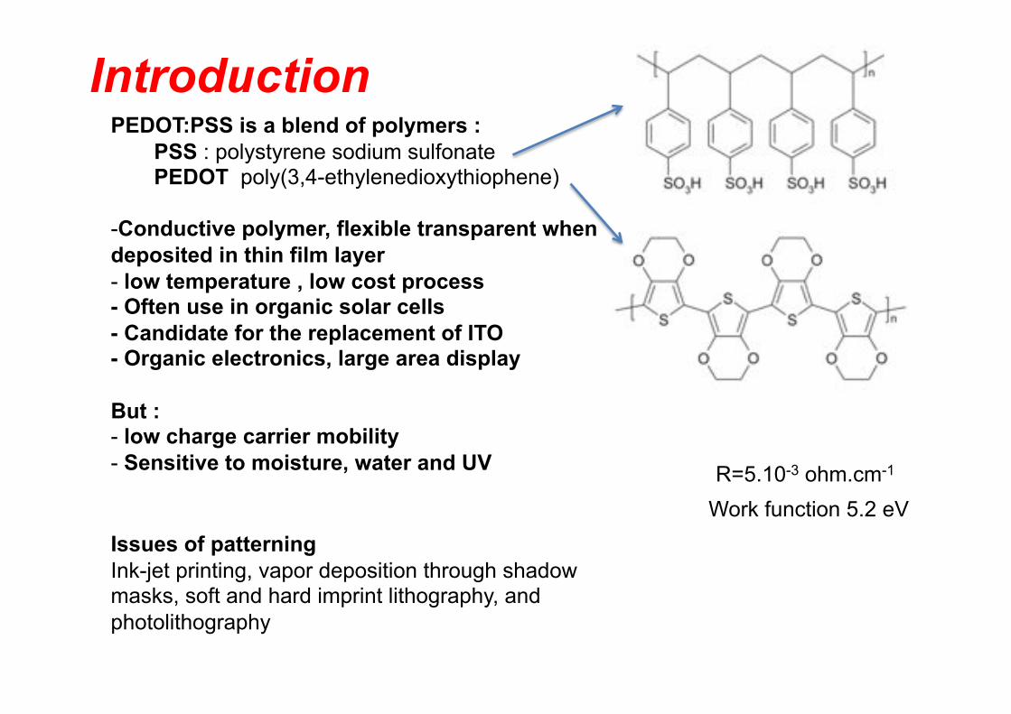
Introduction PEDOT:PSS is a blend of polymers : PSS : polystyrene sodium sulfonate PEDOT poly(3,4-ethylenedioxythiophene)
- Conductive polymer, flexible transparent when deposited in thin film layer - low temperature , low cost process - Often use in organic solar cells - Candidate for the replacement of ITO - Organic electronics, large area display
But : - low charge carrier mobility - Sensitive to moisture, water and UV
Work function 5.2 eV R=5.10-3 ohm.cm-1
Issues of patterning Ink-jet printing, vapor deposition through shadow masks, soft and hard imprint lithography, and photolithography
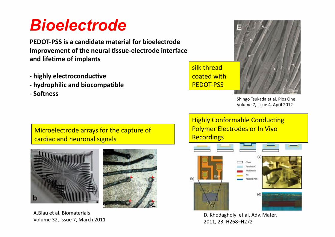
Bioelectrode PEDOT&PSS(is(a(candidate(material(for(bioelectrode(
Improvement(of(the(neural(<ssue&electrode(interface(
and(life<me(of(implants(
&(highly(electroconduc<ve((
&(hydrophilic(and(biocompa<ble(
&(So?ness(Shingo&Tsukada&et&al.&Plos&One&Volume&7,&Issue&4,&April&2012&&
A.Blau&et&al.&Biomaterials&Volume&32,&Issue&7,&March&2011&
D.&Khodagholy&&et&al.&Adv.&Mater.&2011,&23,&H268–H272&&
Microelectrode&arrays&for&the&capture&of&cardiac&and&neuronal&signals&&
Highly&Conformable&ConducTng&Polymer&Electrodes&or&In&Vivo&Recordings&
silk&thread&coated&with&PEDOT7PSS&

PEDOT:PSS deposition Spincoa<ng(
3000(rpm(Th=100nm(((
and(drying(on(hotplate(125°C(
WeIng(issue(can(be(solved(by(adding(IPA(
Additives for increasing conductivity
Ethylène glycol C2H6O2 Glycerol C3H8O3 Sorbitol C6H14O6 Dimethyl Sulfoxide DMSO C2H6OS Erythritol C4H10O4
Mean Resistivity PEDOT:PSS only : R=6 Ω.cm-1
Mean Resistivity PEDOT:PSS / DMSO R=5.10-3 Ω.cm-1
Mean Resistivity PEDOT:PSS / EG R=6.10-3 Ω.cm-1
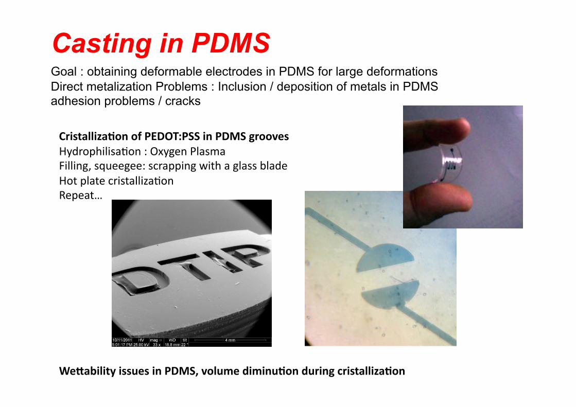
Casting in PDMS Goal : obtaining deformable electrodes in PDMS for large deformations Direct metalization Problems : Inclusion / deposition of metals in PDMS adhesion problems / cracks
Cristalliza<on(of(PEDOT:PSS(in(PDMS(grooves(
HydrophilisaTon&:&Oxygen&Plasma&Filling,&squeegee:&scrapping&with&a&glass&blade&Hot&plate&cristallizaTon&Repeat…&
WeNability(issues(in(PDMS,(volume(diminu<on(during(cristalliza<on(((

Casting from PDMS Deposition of PEDOT:PSS patterns from a PDMS scaffold
Liquid PEDOT:PSS droplet
Pressing
Hot plate cristallization
Residues cleaning : Reactive ion etching
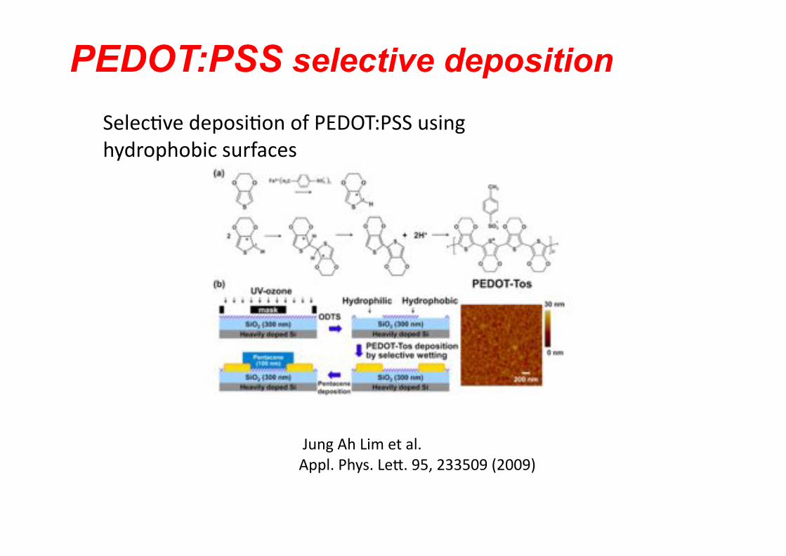
PEDOT:PSS selective deposition
&Jung&Ah&Lim&et&al.&&Appl.&Phys.&Le^.&95,&233509&(2009)&
SelecTve&deposiTon&of&PEDOT:PSS&using&hydrophobic&surfaces&
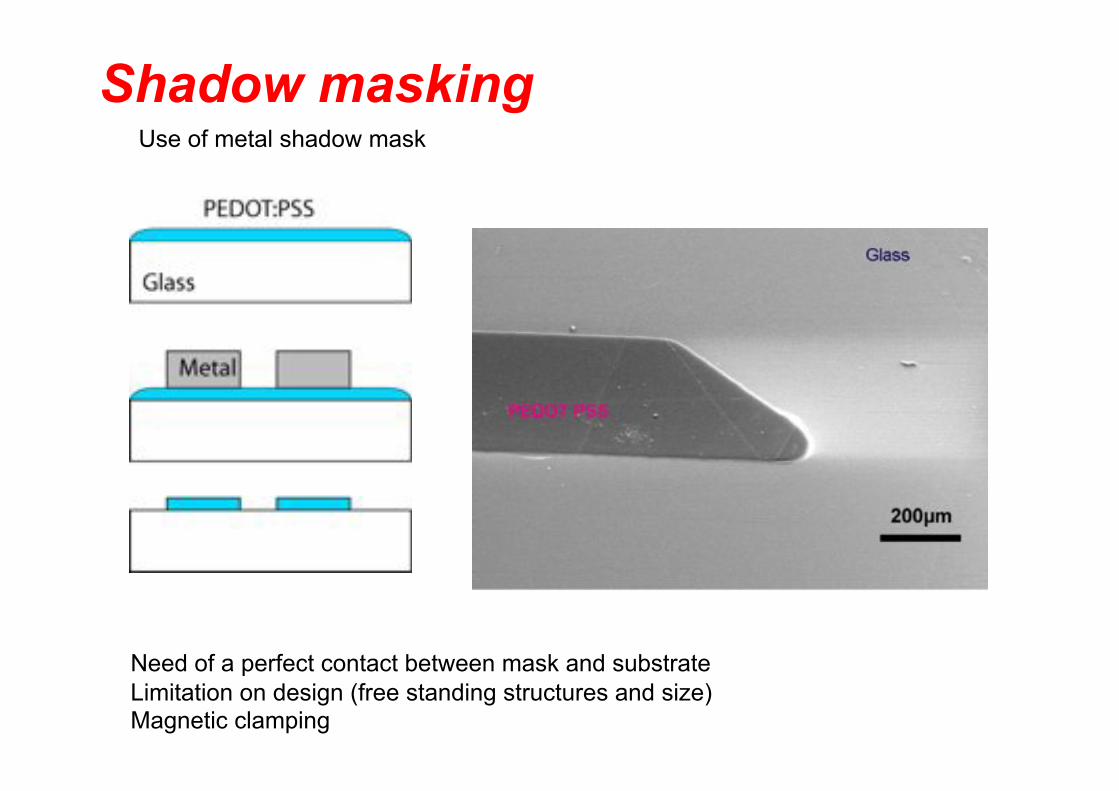
Shadow masking Use of metal shadow mask
Need of a perfect contact between mask and substrate Limitation on design (free standing structures and size) Magnetic clamping
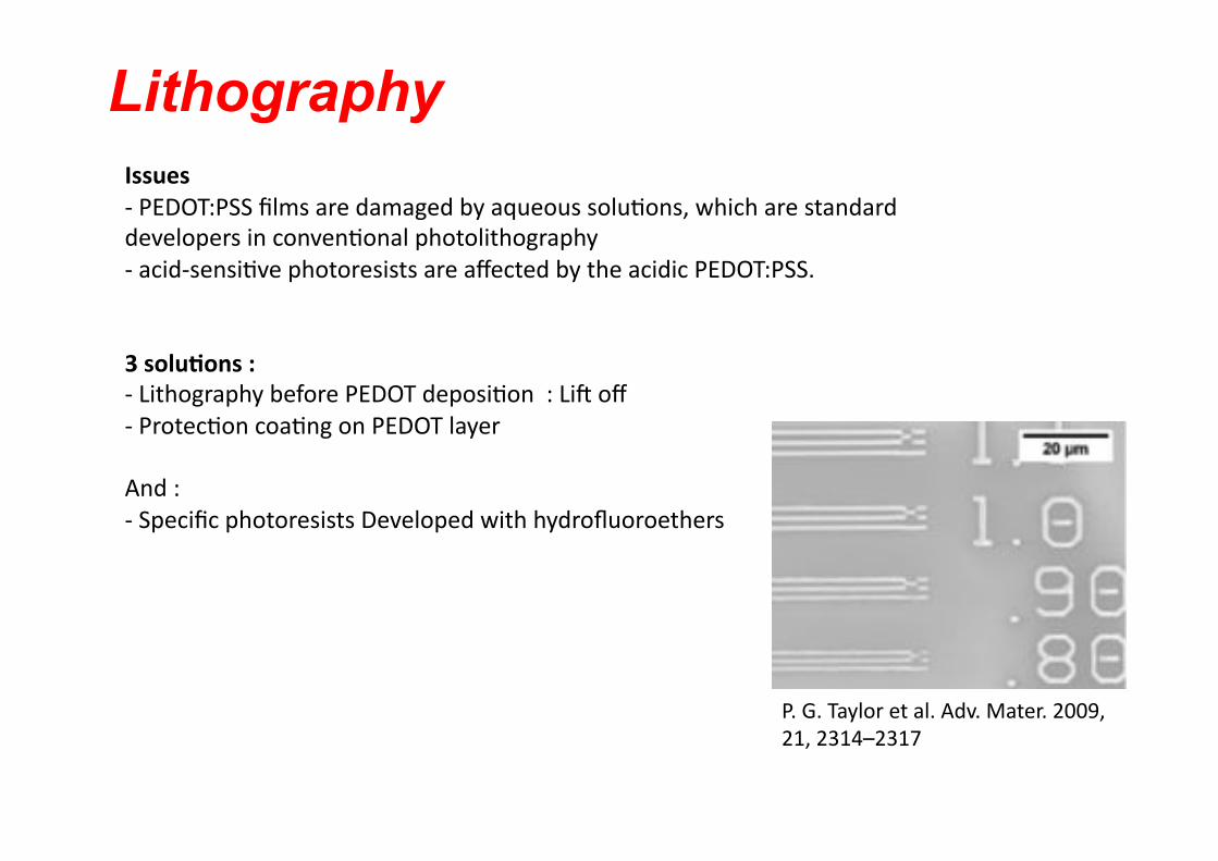
Lithography
P.&G.&Taylor&et&al.&Adv.&Mater.&2009,&21,&2314–2317&
Issues(
7&PEDOT:PSS&films&are&damaged&by&aqueous&soluTons,&which&are&standard&developers&in&convenTonal&photolithography&7&acid7sensiTve&photoresists&are&affected&by&the&acidic&PEDOT:PSS.&
3(solu<ons(:((
7&Lithography&before&PEDOT&deposiTon&&:&Lid&off&7&ProtecTon&coaTng&on&PEDOT&layer&
And&:&7&Specific&photoresists&Developed&with&hydrofluoroethers&
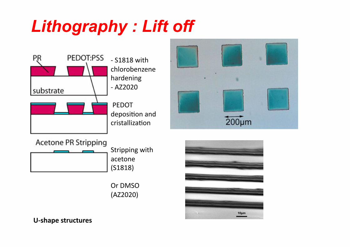
Lithography : Lift off
7&S1818&with&chlorobenzene&hardening&7 &AZ2020&
&PEDOT&deposiTon&and&cristallizaTon&
Stripping&with&acetone&(S1818)&
Or&DMSO&(AZ2020)&&
U&shape(structures&
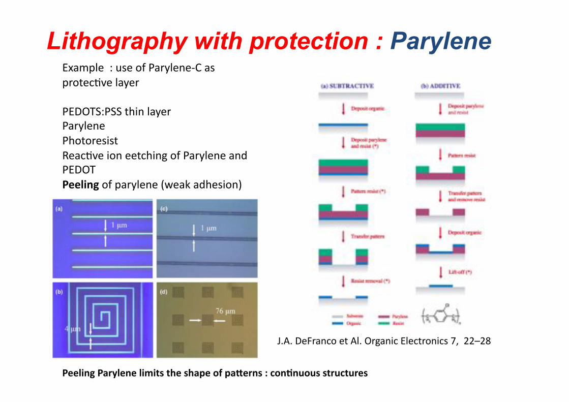
Lithography with protection : Parylene
J.A.&DeFranco&et&Al.&Organic&Electronics&7,&&22–28&
Example&&:&use&of&Parylene7C&as&protecTve&layer&
PEDOTS:PSS&thin&layer&Parylene&Photoresist&&ReacTve&ion&eetching&of&Parylene&and&PEDOT&Peeling(of&parylene&(weak&adhesion)&
Peeling(Parylene(limits(the(shape(of(paNerns(:(con<nuous(structures(
P.&M.&Sousa,&APPLIED&PHYSICS&LETTERS&99,&044104&(2011)&
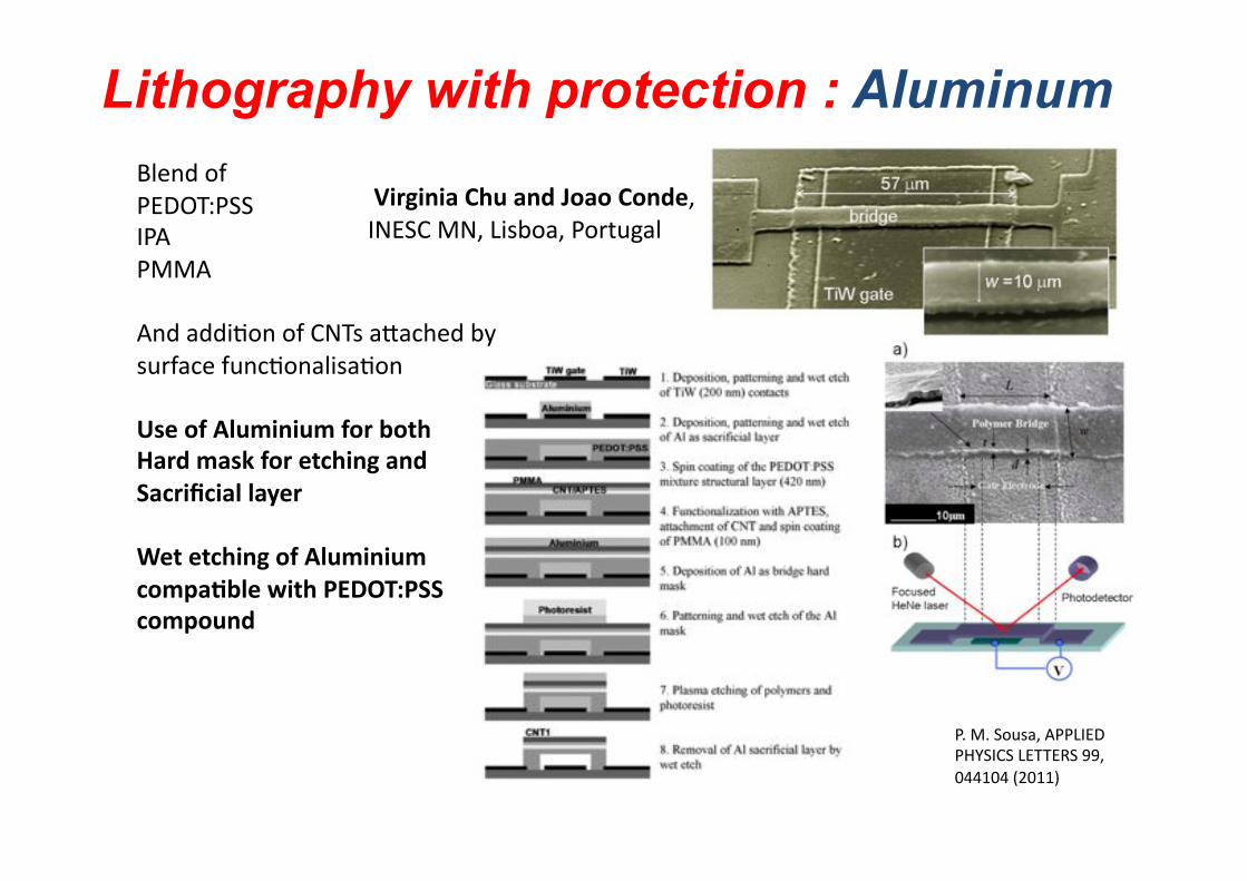
&Virginia(Chu(and(Joao(Conde,&INESC&MN,&Lisboa,&Portugal&
Blend&of&&PEDOT:PSS&IPA&PMMA&
And&addiTon&of&CNTs&a^ached&by&surface&funcTonalisaTon&
Use(of(Aluminium(for(both((
Hard(mask(for(etching(and(
Sacrificial(layer(
Wet(etching(of(Aluminium(
compa<ble(with(PEDOT:PSS(
compound(((((
Lithography with protection : Aluminum

Silicon Nitride protection layer
PEDOT:PSS deposition SiNx PECVD deposition (200°C) 100nm Lithography RIE selective etching CHF3 for SiNx O2 for PEDOT:PSS
Lithography with protection : Si3N4
Flat(profile,(but(requires(precise(etching(control&
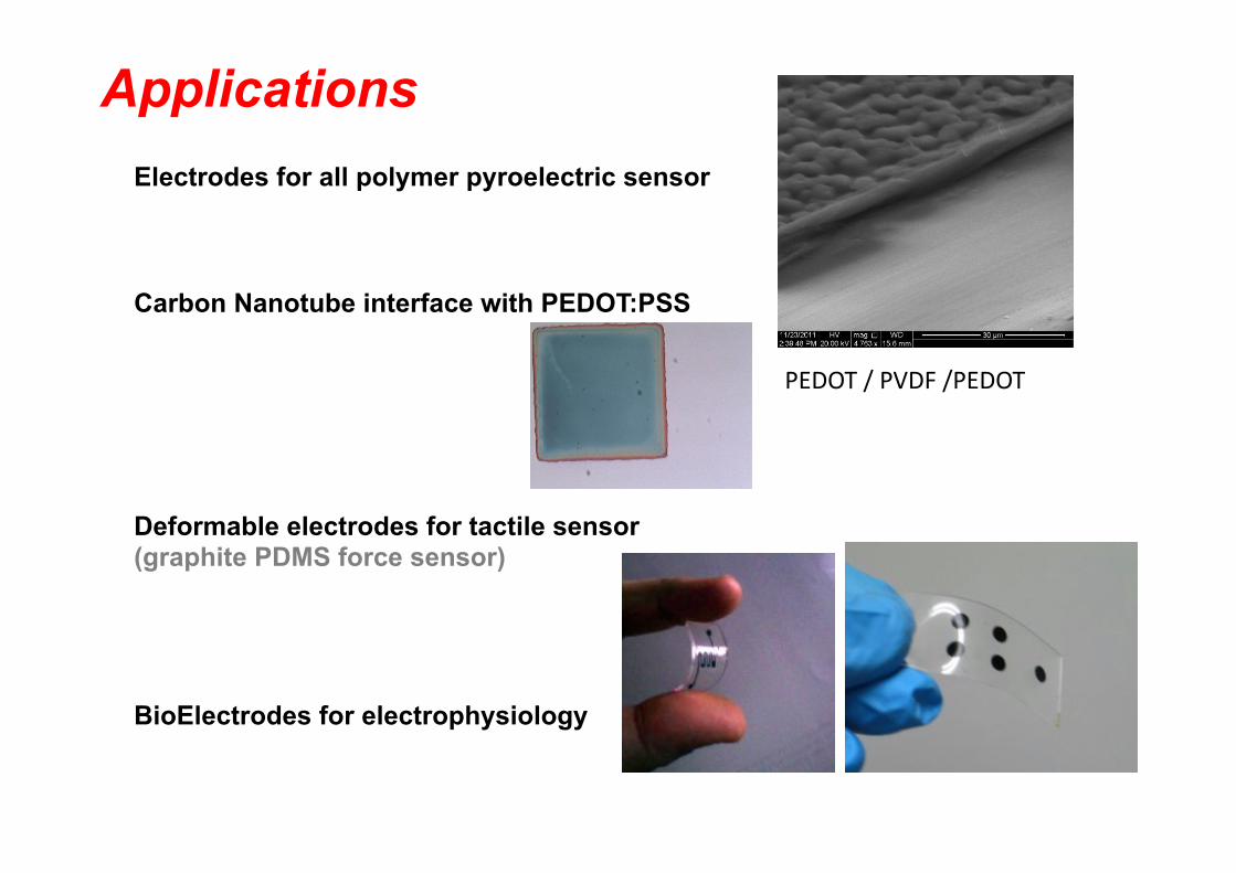
PEDOT&/&PVDF&/PEDOT&
Applications Electrodes for all polymer pyroelectric sensor
Carbon Nanotube interface with PEDOT:PSS
Deformable electrodes for tactile sensor (graphite PDMS force sensor)
BioElectrodes for electrophysiology

Conclusions
PEDOT:PSS is an interesting material for implementation of deformable electrodes in several applications
Patterning techniques includes - Soft lithography - standard lithography / RIE etching with process adaptation
Potential use in bioelectrodes for neuro interface
Further work :
Effect of RIE on polymer, degradation? Best gazes for etching CHF3? CF4? O2