microfluidic laminate-based phantom for dt- · pdf filemicrofluidic laminate-based phantom for...
TRANSCRIPT

Microfluidic laminate-based phantom for diffusion tensor-magnetic resonance imaging
This article has been downloaded from IOPscience. Please scroll down to see the full text article.
2011 J. Micromech. Microeng. 21 095027
(http://iopscience.iop.org/0960-1317/21/9/095027)
Download details:
IP Address: 155.98.20.40
The article was downloaded on 11/04/2012 at 18:04
Please note that terms and conditions apply.
View the table of contents for this issue, or go to the journal homepage for more
Home Search Collections Journals About Contact us My IOPscience

IOP PUBLISHING JOURNAL OF MICROMECHANICS AND MICROENGINEERING
J. Micromech. Microeng. 21 (2011) 095027 (11pp) doi:10.1088/0960-1317/21/9/095027
Microfluidic laminate-based phantom fordiffusion tensor-magnetic resonanceimagingR Samuel1,3, H J Sant1, F Jiao2, C R Johnson2 and B K Gale1
1 State of Utah Center of Excellence for Biomedical Microfluidics, University of Utah,50 S Central Campus Dr., Rm 2110, Salt Lake City, UT 84112, USA2 Scientific Computing and Imaging Institute, University of Utah, 72 S Central Campus Dr. Rm 3750,Salt Lake City, UT 84112, USA
E-mail: [email protected], [email protected], [email protected], [email protected] [email protected]
Received 15 April 2011, in final form 5 July 2011Published 19 August 2011Online at stacks.iop.org/JMM/21/095027
AbstractThis paper reports fabrication of a magnetic resonance imaging (MRI) phantom created bystacking of multiple thin polydimethylsiloxane (PDMS) layers. PDMS is spin-coated on SU-8molds to obtain the desired layer thickness and imprints of the microchannel patterns thatdefine the phantom geometry. This paper also identifies the unique challenges related to thefabrication and assembly of multiple thin layers and reports for the first time assembly of alarge number of thin laminates of this nature. Use of photolithography techniques allows us tocreate a wide range of phantom geometries. The target dimensions of the phantoms reportedhere are two distinct stacks of 30 thin PDMS layers each of 10 μm thickness with either(i) curved 5 μm × 5 μm microchannels with 8.7 μm spacing, or (ii) straight 5 μm × 5 μmmicrochannels with 3.6 μm spacing. SEM scans of the assembled phantoms show openmicrochannels and a monolithic cross section with no visible interface between PDMS layers.Based on the results of diffusion tensor magnetic resonance imaging scanning, the anisotropicdiffusion of water molecules due to the physical restriction of the microchannels was detected,which means that the phantom can be used to calibrate and optimize MRI instrumentation.
(Some figures in this article are in colour only in the electronic version)
1. Introduction
Molecular diffusion refers to the random movement ofmolecules through space, driven by their internal thermalenergy. It is a process that is highly sensitive to the physicalstructure of the microscopic environment. Diffusion tensormagnetic resonance imaging (DT-MRI) has been used tomeasure the diffusivity of water and metabolites noninvasivelyat microscopic length scales [1, 2]. DT-MRI measuresthe restricted random Brownian motion of water molecules[3]. During the MRI measurement interval (ms), the watermolecule can diffuse a distance of 5–20 μm, while thediffusion tensor at each voxel measures the local diffusionprofile. For the standardization of DT-MRI machines, standard3 Author to whom any correspondence should be addressed.
physical models (also known as phantoms) are required withwell-defined microscopic architecture. A proposed design foran MRI phantom is shown in figure 1. Artificial fiber diffusionphantoms have been fabricated using hemp, linen, polyamide,polyester, polyethylene and rayon [1]. However, it is importantto develop artificial phantoms that can be reproduced in orderto produce a particular MRI scan result, which will help inefforts for the validation of MRI technology. The qualityof a phantom is typically dependent on the anisotropy ofwater diffusion (restricted random Brownian motion of watermolecules) and the amount of water in the phantom, which inturn determines the phantom design. The size of the PDMS-based phantom developed in this work was 1.5 cm × 1.5 cm ×0.3 mm to obtain an image of about 15 × 15 voxels of 0.5 mmor 1 mm cubes.
0960-1317/11/095027+11$33.00 1 © 2011 IOP Publishing Ltd Printed in the UK & the USA

J. Micromech. Microeng. 21 (2011) 095027 R Samuel et al
Figure 1. Left: a 3D schematic of the envisioned multilayer phantom (not to scale), the targeted dimensions are height: 0.3 mm, width:1.5 cm, length: 1.5 cm. Each layer is 10 μm thick with 5 μm × 5 μm channels. Spacing between channels (3.6 or 8.7 μm) and theorientation (curved channels or straight channels) is varied for each phantom. The diffusional direction of water molecules is shown by thedouble-headed arrow. Right: a magnified view of the cross-sectional area marked by a black square in the left picture (small microchannelscan be observed). With microfabrication techniques, we can reproduce such highly parallel, multilayered microchannels consistently.
PDMS is a popular material for biomedical applicationsbecause of its outstanding material properties and thesimplicity with which it can be cast onto microstructured molds[4]. Most PDMS-based microfabricated products requiremicromolding of microchannels in PDMS layers and laterbonding of these layers to glass/silicon or to another PDMSsurface for the realization of the final product. Currently,soft lithography-based PDMS layer fabrication uses twoapproaches: spin-casting or the membrane-sandwich method[5, 6]. However, PDMS has its own microfabricationchallenges. Peeling off a freely suspended spin-cast, ∼10 μmthick PDMS layer, from a molding substrate such as a siliconwafer is a significant challenge. Such thin layers are verydelicate and once torn are easily damaged during the peelingprocess [7]. However, in some cases PDMS layers as thinas 70 nm and without embedded structures have been spun-cast and later peeled off. Demolding these layers requiresthe presence of an adhesion reduction layer between PDMSand the silicon substrate [8]. There are further hurdles instacking these ultra-thin, spin-coated layers—the occurrenceof air bubbles and wrinkles. However, researchers have beenable to efficiently stack five relatively thick (120 μm) PDMSlayers for 3D microfluidic channel realization by using themembrane-sandwich method [6], and a variation of the samemethod was used to assemble six (50 μm thick) layers [9].In the membrane-sandwich method, uncured PDMS is placedbetween a SU-8 mold and a flat rigid plate. The flat rigid plateis pressurized from the top, which in turn squeezes the PDMSin between the mold and plate. Different layer thickness canbe achieved by varying the applied pressure. After applyingthe required pressure, the whole assembly is heated and thePDMS layer cures, which is then peeled off the mold. Themembrane-sandwich method [5, 6] allows great control in thefabrication process [10] but is limited to relatively thick andmechanically weaker layers (>20 μm) [11].
The geometry of the phantoms described in this paper wasdetermined by the requirement of high MRI signal to noiseratio. During MRI scanning, high signal to noise ratios canbe achieved if the phantoms can retain large amounts of water(i.e. a high ratio of combined microchannel volume/phantomvolume) and high diffusion anisotropy. Consequently,each phantom layer necessitated a dense array of parallel
microchannels and the layers needed to be as thin as couldbe handled easily and manufactured with high reproducibility.Based on these design criteria, the thickness of the PDMSlayers was set to 10 μm. Fabricating a 10 μm thick layerwith thousands of 5 μm × 5 μm (approximately) patternedparallel microchannels in an area of 1.5 mm × 1.5 mm is morefeasible when they are spin-cast on SU-8 molds in standardphotoresist spinners (available in almost all microfabricationlabs) than with the previously mentioned membrane-sandwichmethods (with reference to their relatively large microchanneldimensions, larger layer thickness and low microchanneldensity per layer) [6, 9]. Another variation of the membrane-sandwich approach used by Zhang et al [9] for thin PDMSlayer stacking is the use of fluorosilanes for selective transferof the PDMS microstructure from mold to final assembly withan intermediate transfer step [9]. Success of such an approachremains to be investigated when very thin PDMS layers(<20 μm) for a dense network of molded microchannels needto be assembled. In contrast, our approach utilizes spin-castPDMS layers that are mechanically stronger than standardcasting as the stretching of polymer chains in the radialdirection on spinning at high spin speeds improves mechanicalstrength significantly [11]. This helps in proper release of thehighly patterned layer from the mold, without any damage andpermanent deformation of the layer. However, stacking a largenumber (∼30) of thin (<20 μm) spin-cast patterned PDMSlayers has so far not been demonstrated in the literature.
This work reports a unique fabrication process forfabricating patterned 10 μm thick PDMS layers cast from astandard SU-8 soft lithographic mold into a 30-layer laminate.Each layer includes thousands of microchannels that are filledwith deionized (DI) water. The layers are created usingconventional spin-casting techniques on a large mold area andlater stacked and bonded by a repeatable and uniform stackingmethod. The unique feature of this method is the use of athick transfer ring, made from PDMS as well to transport andassemble the thin PDMS layers while allowing the use of aunique air-pressure technique to bond stacked layers activatedby a corona discharge. This special air-pressure techniquehelps in stacking the layers without any trapped air bubbles orwrinkles. When the 30 layers are stacked, they are immersedin DI water and then sealed in a PDMS block before being used
2

J. Micromech. Microeng. 21 (2011) 095027 R Samuel et al
Figure 2. A schematic diagram of the phantom fabrication showing the PDMS softlithography steps, the use of the SU-8 mold and thetransfer ring for the assembly of thin PDMS layers.
as a MRI phantom. By taking MR images of this phantom,researchers will be able to improve imaging characteristics ofMRI machines.
2. Methods
The fabrication process used in this work is simple but can bebest explained using three separate illustrations (figures 2–4),with the main steps designated in order and identified with astep number from A–M which is referred to in the descriptionof the relevant process step.
2.1. SU-8 mold fabrication and pretreatment (step A, figure 2)
The individual patterned microfluidic laminates were createdusing SU-8 micromolding and PDMS soft lithographytechniques in a normal room environment on a 4 inch siliconwafer (Silicon Qwest International Inc., Santa Clara, CA).
SU-8 2005 (Micro Chem, Newton, MA) was spun on thesilicon wafer at 2500 rpm for 30 s at a ramp of 300 rpm s−1
and soft baked at 95 ◦C for 2 min on a leveled hot plate.The phantoms were fabricated using two mask patterns. Onemask pattern generated a SU-8 mold with curved 5 μm widechannels with 8.7 μm channel spacing. The other mask patterngenerated straight 5 μm wide channels with 3.6 μm channelspacing. An exposure bandpass filter (PL-360 LP, OmegaOptical, Brattleboro, VT) was used to allow transmission of365 nm wavelength light. A dose of 100 mJ cm−2 was usedto expose ∼5 μm thin SU-8 through the appropriate mask.The exposure time was set to 9 s on a mask aligner (EV-420,EV Group Inc. Tempe, AZ). After exposure, the substratewas post-baked for 3 min at 95 ◦C and later developed in theSU-8 developer for 2 min followed by isopropanol rinsing anddrying with nitrogen gas. The patterned wafer was hard bakedon a hotplate at 150 ◦C for 2 min.
Prior to micromolding the PDMS, the SU-8 mold wascoated with a thin layer (∼ 400 nm) of Cytop (CTL-809M,
3

J. Micromech. Microeng. 21 (2011) 095027 R Samuel et al
Figure 3. Summary of the fabrication process, depicting stacking of 30 layers to make six separate five-layer stacks. This approachimproves the yield as any error during fabrication is limited to smaller stacks.
Asahi Glass Co. Ltd, Ibaraki, Japan). Cytop acts as anadhesion reduction layer between PDMS and silicon [8]. Afterthe SU-8 hard bake, Cytop was spin-coated at 5000 rpm for1 min with a 300 rpm s−1 ramp and cured at 180 ◦C on aleveled hotplate for 1 h.
2.2. PDMS molding (step B, figure 2)
Once the SU-8 mold was completed, the next step was to castthe PDMS layers on the mold. All the PDMS (Slygard R© 184Silicone Elastomer, Dow Corning, MI) used in this paper hadthe PDMS base to curing agent ratio of 5:1.
For layer fabrication, uncured PDMS was spun on theSU-8 mold with the overlying Cytop layer at 5000 rpm for1 min (∼10 μm thick) (step B). The layer was cured at100 ◦C for 10 min on a hot plate with an aluminum foil-coverto minimize foreign particulate contamination.
2.3. PDMS layer picking and assembly (steps C and D,figure 2)
At ∼10 μm, PDMS spin-cast layers have significant stress andare difficult to handle and tend to fold onto themselves. Oneof the challenges in this work was to remove such thin PDMSlayers off the 4 inch SU-8 mold (large surface area) without
damaging the very small molded microchannels on the layeror the layer itself or any of the microstructures across thesubstrate. To facilitate easy removal of the thin PDMS layer, a3 mm thick transfer ring was made which had an outer diameterof 135 mm and inner diameter of 68 mm. The transfer ringwas used as a holder that bonds the ends of the PDMS layerto lift the thin layer. Furthermore, the transfer ring provided amechanical support to the thin layer after peeling it off fromthe mold. The ring was made using the standard PDMS castingprocess to make a PDMS slab and then a razor was used tocore out the ring-shaped PDMS. In preparation for picking upthe thin layers, uncured PDMS was applied using a spatula tothe ends of the PDMS layer overlying the SU-8 mold. Theuncured PDMS was applied such that it formed a ring on theoverlying PDMS layer. This ring of uncured PDMS had anouter diameter the same as that of the mold (100 mm) and innerdiameter of approximately 75 mm. In this way, the uncuredPDMS did not interfere with the patterned microstructures (inthe center of the layer) on the thin PDMS layer, overlying onthe SU-8 mold. The transfer ring was placed on the mold suchthat it made a good contact with the uncured PDMS (step C).Both the mold and transfer ring on top of the PDMS wereplaced on a hotplate at 100 ◦C for 5 min. This process resultedin adhesion of the thin layer to the transfer ring. For PDMSlayer removal, the transfer ring was first gently separated from
4

J. Micromech. Microeng. 21 (2011) 095027 R Samuel et al
Figure 4. Summary of the fabrication process, depicting stacking of six five-layer stacks to make a single 30-layer stack and encasement ofthe stack by a PDMS cap for the realization of the final product.
the mold’s edges. The transfer ring was then slowly pulled upfrom the mold from one end to the other, and the thin PDMSlayer was brought with it, ensuring peeling off the thin PDMSlayer without tearing (step D).
2.4. Stacking of the layers (step E, figure 2; steps F–H,figure 3; steps I–L, figure 4)
Each molded layer had up to 16 distinct phantom designs on it.A single microfluidic phantom was a 30 layer-laminate of onlyone of these 16 distinct designs (we used two of these designsto make two distinct microfluidic phantoms mentioned in thispaper).
The main challenge of this work was the stacking of largenumber of highly flexible thin PDMS layers (at least 30 layers,to reach the minimum stack height for the MRI scanner usedin this study), without the presence of any trapped air bubbles,wrinkles and delamination of the bonded layers. The stackingmethodology had to be simple enough to be carried outsidethe clean room without the use of any complicated hardware,so as to be cost effective.
A Petri dish (Part 0875713, Fisher Scientific, Pittsburgh,PA) was used as the base while stacking the layers, as thepolystyrene Petri dishes have low adhesion between Petri dishsurface and cured PDMS, which provides an easy removal ofthe stacked PDMS laminates. After peeling off the PDMSlayer from the mold, it was placed on a Petri dish gentlyby using air pressure to lay it flat (step E). Care was takento make sure that no air bubbles formed between the PDMSlayer and the Petri dish. Wrinkles and bubbles were avoided
by bringing one end of the suspended layer in contact withthe Petri dish surface and pressing it flat with air pressure(using a low-pressure compressed-air nozzle), starting fromone end and progressively moving to the other end. The PDMSlayer was separated from the transfer ring with a knife cut torelease the transfer ring. There was enough room for theknife cut, so as to avoid any permanent damage to the moldedstructures located near the center of the wafer. For addition ofthe second layer, both mating surfaces were activated witha corona/glow discharge (LM4243-05, Enercon IndustriesCorporation, WI). The second layer was gently placed on topof the first layer using the same air-pressure technique andknife cut as described earlier (step F). No special hardware wasused for layer alignment and was done by the naked eye usingphantom borders as alignment marks. The same procedurewas repeated to assemble six separate five-layer stacks (stepG). The phantom design for this study required a stack of 30thin layers of PDMS microstructures. For optimal phantomperformance, each layer had to be flat without any wrinkles,trapped air bubbles or any layer detachment. For efficient layerstacking and consistent fabrication yield, six separate stacksof five layers each were fabricated and then stacked on eachother to make a single 30-layer stack.
To facilitate the handling of five-layer stacks, a smallerPDMS transfer ring was used. Corona (glow discharge)treatment was done on top of one of the five-layer stacksto be used as a base stack on which other five-layer stackswould be stacked. One side of the smaller transfer ring wasalso activated by corona discharge and that face was placed ontop of the base stack and pressed for 2 min before peeling off
5
J. Micromech. Microeng. 21 (2011) 095027 R Samuel et al
the base stack from the Petri dish (steps H and I). The bottomsurface of the base stack which was previously in contactwith the Petri dish was activated with corona and placed ontop of a cured and corona-treated PDMS substrate of 10 mmthickness (step J). The base stack was laid flat on the PDMSsubstrate using the same compressed air-pressure technique aswas described earlier and cut free from the transfer ring witha sharp knife. The entire assembly procedure was repeateduntil a phantom prototype with 30 layers was created (steps Kand L).
2.5. Device testing
To ensure that the microchannels had not collapsed andwere filled with DI water, scanning electron microscope(SEM) scans of a phantom model’s (five-layer stack) crosssection after immersing it in a pool of polystyrene beadsand DI water were collected. The purpose was to fill themicrochannels with water, which will carry the polystyreneparticles along with it. When the water is evaporated, theentrained polystyrene particles can be detected by imaging thecross section (approximately mid-way across the length ofthe channels) of the five-layer stack, which will confirm thatthe channels are being filled with DI water.
To accomplish the filling of the phantom with water, thephantom model was placed in a Petri dish. The Petri dish wasfilled with DI water containing 10% (by volume) polystyrenemicrospheres of 0.202 μm diameter (Part 07304, PolysciencesInc., PA). The Petri dish was placed in a vacuum chamber atmoderate vacuum (–26 inHg) for 2 min, which degassed themicrochannels and filled them with water. The stack waswashed with DI water and dried in an oven at 62 ◦C for 2 h.Later, the stack was cut in the middle, across the channels bya fine blade. The newly exposed cross section was imaged bya SEM.
2.6. Device assembly (step M, figure 4)
The 30 layers laminated in the end of step L in figure 4 werepressed flat by a small roller to ensure that all the layerswere evenly bonded and no layer delamination occurred. Themicrochannels of the phantom prototypes were opened bycutting the edges of the channels with a fine blade. Theentire phantom was sealed using a PDMS cap that was corona-bonded to the PDMS substrate (step M). The PDMS cap alsooutlined a reservoir area around the phantom that containedDI water. A 2 mm thick PMMA (Polymethyl methacrylate)sheet (25 mm × 25 mm) was bonded with double-sided tapein a polystyrene Petri dish, to make a mold for the PDMS cap.The entire phantom assembly was cured overnight in an ovenat 65 ◦C to improve the bond strength between different layersof phantom and ensure a leak-proof seal between the PDMSsubstrate and the cap. After cooling of the phantom prototype,DI water was injected through the PDMS cap using a syringewith a 27G needle until the reservoir containing the phantomwas completely filled. The holes made by the syringe needlewere sealed using a silicone elastomer (734 Flowable Sealant,Dow Corning, MI) to prevent any DI water leaking out of thereservoir. The submerged phantom was placed in a vacuum
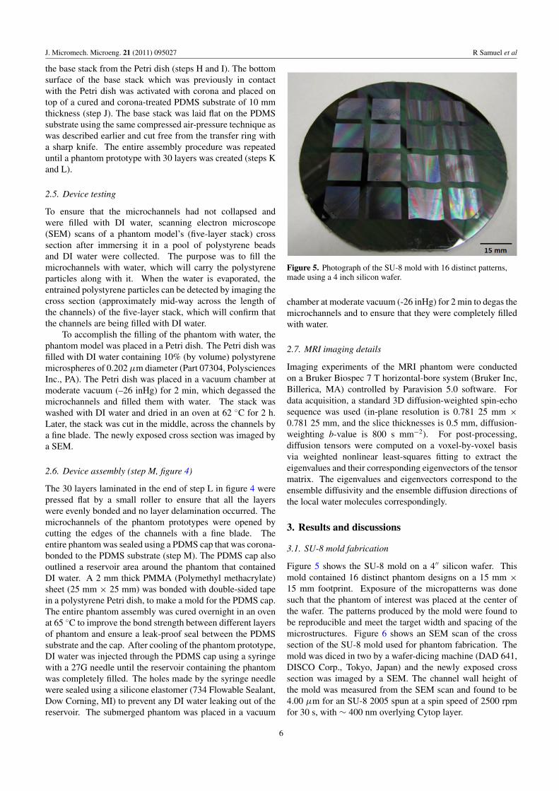
Figure 5. Photograph of the SU-8 mold with 16 distinct patterns,made using a 4 inch silicon wafer.
chamber at moderate vacuum (-26 inHg) for 2 min to degas themicrochannels and to ensure that they were completely filledwith water.
2.7. MRI imaging details
Imaging experiments of the MRI phantom were conductedon a Bruker Biospec 7 T horizontal-bore system (Bruker Inc,Billerica, MA) controlled by Paravision 5.0 software. Fordata acquisition, a standard 3D diffusion-weighted spin-echosequence was used (in-plane resolution is 0.781 25 mm ×0.781 25 mm, and the slice thicknesses is 0.5 mm, diffusion-weighting b-value is 800 s mm−2). For post-processing,diffusion tensors were computed on a voxel-by-voxel basisvia weighted nonlinear least-squares fitting to extract theeigenvalues and their corresponding eigenvectors of the tensormatrix. The eigenvalues and eigenvectors correspond to theensemble diffusivity and the ensemble diffusion directions ofthe local water molecules correspondingly.
3. Results and discussions
3.1. SU-8 mold fabrication
Figure 5 shows the SU-8 mold on a 4′′ silicon wafer. Thismold contained 16 distinct phantom designs on a 15 mm ×15 mm footprint. Exposure of the micropatterns was donesuch that the phantom of interest was placed at the center ofthe wafer. The patterns produced by the mold were found tobe reproducible and meet the target width and spacing of themicrostructures. Figure 6 shows an SEM scan of the crosssection of the SU-8 mold used for phantom fabrication. Themold was diced in two by a wafer-dicing machine (DAD 641,DISCO Corp., Tokyo, Japan) and the newly exposed crosssection was imaged by a SEM. The channel wall height ofthe mold was measured from the SEM scan and found to be4.00 μm for an SU-8 2005 spun at a spin speed of 2500 rpmfor 30 s, with ∼ 400 nm overlying Cytop layer.
6

J. Micromech. Microeng. 21 (2011) 095027 R Samuel et al
Figure 6. Picture showing SEM scan of the cross section of dicedend of the SU-8 mold.
It should be noted that the same SU-8 mold wasused to obtain all 30 layers for fabricating a microfluidicphantom. No damage or permanent deformation of the mold’smicrostructures was observed in the entire fabrication processof a single phantom.
3.2. PDMS molding: layer thickness and strength
In order to produce layers with precise thickness, the spinnerwas calibrated to achieve near-10 μm thick layers. Figure 7shows a spin curve for PDMS spun on a 100-mm silicon waferwith a 400 nm overlying layer of Cytop. The thickness ofeach PDMS layer was measured by imaging the cross sectionof the layer under an optical microscope (Nikon Optiphot88, Nikon Instruments Inc., Melville, NY). This method hasbeen demonstrated to have reasonable accuracy (0.2%) for thinPDMS layer thickness measurements [12].
To determine the average thickness of each layer of thephantom, thicknesses of three individual five-layer stacks weremeasured at three distinct points. A total of nine data points
Figure 7. Plot of PDMS layer thickness (μm) versus spinner spinspeed (RPM). The PDMS used for this work has the base to curingagent ratio of 5:1.
Figure 8. Picture of a PDMS transfer ring (weighing 30 g) beingsupported by ∼10 μm thin membrane at the tip of a finger.
were used to obtain an average individual layer thickness as11.6 ± 0.5 μm.
Interestingly, these thin PDMS membranes even withphantom microstructures proved to be very strong even at∼10 μm thickness. Figure 8 shows a picture of the PDMSlayer attached to the transfer ring (weighing 30 g) being heldat the center with the tip of a finger. This result is in accordwith Liu et al [11] and very useful while picking up the layersand aligning them to fabricate a stack of multiple laminates.
3.3. PDMS layer picking and assembly
Figures 8 and 9 show the transfer ring that is used to pick upindividual PDMS layers from the SU-8 mold. While someof the microstructures are lost because of the transfer ringoverlay (figure 9), the single layer can be lifted off the moldcleanly without any effect to the layer structural integrity. Inaddition, this loss of microstructures due to the transfer ringoverlay did not warrant any changes to the phantom designas the patterns in the center of the mold were of interest andused to fabricate all the phantoms we described in this paper.The usable phantom can be selected easily while aligning themask to the SU-8 mold during exposure. However, the size ofthe uncured adhesive PDMS ring can be further optimizedto provide the least overlay of the transfer ring onto themold. Furthermore, a larger wafer can also be used to leaveenough distance from the edge of the mold to achieve the sameeffect.
The PDMS ring was 3 mm thick. We found that a thickerPDMS ring would not be flexible enough to facilitate peelingoff the thin layers, while a thinner ring would be too flexibleto provide sufficient mechanical support to avoid folding of
7

J. Micromech. Microeng. 21 (2011) 095027 R Samuel et al
Figure 9. Picture of a PDMS transfer ring used to support and peelthe thin layers of PDMS with microstructures. A supported PDMSlayer with 16 distinct patterns (molded areas) can be seen in thepicture.
the thin layer on itself. We were able to peel off at least 20layers from a single PDMS ring before discarding it. Afterpeeling off about 20 layers, the PDMS ring was not ableto bond evenly to the thin layers and resulted in increasedtearing of the thin layers during the peeling process. Bondingof the PDMS transfer ring to the thin PDMS layer on theSU-8 mold (shown in figure 5) was crucial for successfulremoval of the layer from the SU-8 mold. The bond hadto be sufficiently strong and uniform at the ring and layerinterface to overcome the stresses during peeling withouttearing. We used two approaches to bond the PDMS ring to thePDMS layer overlying on the SU-8 mold: corona-dischargemethod and uncured PDMS as an adhesive. While the corona-discharge method was fast, it resulted in burnt PDMS particleson the thin layers (overlying the SU-8 mold) resulting in adamaged surface, which made the layer peeling very difficult.For this reason, a thin layer of uncured PDMS was used asan adhesive to bond the transfer ring to the thin layer on
Figure 10. Image of a SEM scan of a five-layer stack of the PDMS layer showing the measured geometrical dimensions.
the SU-8 mold. Furthermore, different types of PDMS-to-PDMS bonding techniques have been evaluated for their bondstrengths and using uncured PDMS as an adhesive for bondinghas been shown to have the highest bond strength [13].
3.4. Stacking of the layers
The thin PDMS layers (containing microchannels) needed tobe stacked with the least axial misalignment. The stackingin this case was done with the naked eye (with phantomborders as alignment marks) and may have some minor axialmisalignments, but these misalignments can be reduced bystacking under a microscope or by utilizing an aligner speciallydesigned to align PDMS layers [14]. The angular alignmentof the microchannels along the length is very important forthis application such that all the channels should point in thesame direction to achieve high resolution and accuracy of theMRI scan. In future, a PDMS aligner may be used for moreaccurate alignment.
Figure 10 shows SEM (Quanta 600 FEG, FEI, OR)scans of the phantom model composed of a five-layer stack.The channels have a smooth trapezoidal cross section. Thetrapezoidal cross section is due to the overlying 400 nm Cytoplayer, which was spin-coated after the SU-8 mold was madeby photolithography. While the trapezoidal cross sectionof the channels does not affect the phantom performance, athinner passivation layer can be obtained using fluoropolymers(monolayer thickness) that can be deposited by chemical vapordeposition [15], ion-sputtering deposition [16] or vacuumdeposition [17] and subsequent evaporation if needed. Theeffect of using such a deposition approach on PDMS thinlayer peeling remains to be investigated. Nevertheless, thelarge aspect ratio (channel length to height) and not themicrochannel profile ensures anisotropic diffusion, the keyrequirement for MRI phantoms. Figure 11 shows the SEMscan of a 16-layer stack (consistent bonding between eachindividual layer should be noted). Figure 11 clearly shows nodelamination for a stack of 16 layers, an important achievementfor successful phantom fabrication.
8

J. Micromech. Microeng. 21 (2011) 095027 R Samuel et al
Figure 11. Image of a SEM scan of a 16-layer PDMS stack; thestack of layers after curing results in a monolithic structure with novisible interface separating the layers.
Figure 12. Images of SEM scans of microchannel cross sections showing polystyrene particles stuck on channel walls (particles marked bycircles).
In figure 10, the height of the channels in the layers is3.57 μm and about 0.43 μm smaller than the channel wallheight (4.00 μm) in the mold. Possible reasons for this0.43 μm difference are (i) shrinkage of PDMS on curingat a reasonably high temperature (100 ◦C) [18], (ii) relativestretching of the PDMS layer (during the bonding process)with respect to the previous bonded layer and (iii) variationin Cytop coating across the substrate. But such differences inchannel parameters were allowable for this application. Thelayer channel height of 5 μm (if desired) can be obtained byvarying the channel wall height in the mold to compensate forPDMS shrinkage and other effects. Furthermore, a Cytoplayer of thickness less than 400 nm can be obtained byutilizing Cytop thinners available from Asahi Glass Co. Ltd,Japan.
3.5. Device testing
The newly exposed cross sections in the device testing(articulated in section 2.5) of the phantom were imagedby the SEM, and polystyrene particles were seen stuck onthe inner microchannel walls in multiple scans (figure 12).This confirmed that the channels were being filled with DI
9

J. Micromech. Microeng. 21 (2011) 095027 R Samuel et al
Figure 13. The pictures of two assembled MRI phantoms (left: with curved channels, right: with straight channels) along with a US quartercoin. Each phantom is placed in a square water reservoir formed by the PDMS cap and PDMS substrate. No air bubble can be seen in thephantom assembly.
Figure 14. The B0 image (left-hand side) and the diffusion tensor image (right-hand side) of the phantom.
water and the polystyrene particles were carried inside themicrochannels.
3.6. Device assembly
Figure 13 shows the fully fabricated MRI phantoms. Thephantoms are immersed in a PDMS reservoir with DI water.The water infusion and air bubble withdrawal were done with27 G non-coring needles attached to the plastic syringes.
3.7. Diffusion tensor imaging
Figure 14 shows the visualization of the B0 image (left) and thediffusion tensor image (right) of an MRI scan of the phantomshown in figure 13 (left). The diffusion tensor image’s colorvariation depicts the alignment of the major eigenvector indifferent directions (x, y and z directions). From figure 14(left), one can clearly see that the phantom was filled withwater without any air bubbles (as the white area represents
water and dark area represents absence of water). Based onfigure 14 (right) the water molecule shows a certain degreeof anisotropic diffusion. Due to the influence of the imagingbackground noise and possibly the misalignment between eachstack, the anisotropy of each tensor is not as strong as expected.Additionally, the MRI instrumentation may not yet be ableto adequately measure at these scales, so additional softwaredevelopment may be needed to better represent the movementof molecules in the phantom. Finally, the relative volume ofwater in the phantom may need to be increased to increasethe signal available to the MRI instruments. Higher relativevolumes of water would require higher aspect ratio channelswith thicker layers, which is an ongoing effort.
4. Conclusion
A simple method of stacking patterned spin-coated ∼10 μmthick PDMS layers with densely packed microstructures hasbeen developed and demonstrated. The stacking of up to
10

J. Micromech. Microeng. 21 (2011) 095027 R Samuel et al
30 such layers has been performed without the presenceof any trapped air bubbles or wrinkles. The unique layer-stacking technique can be used to fabricate MRI diffusionphantoms as gold standards for MRI machines. Furthermore,the methods developed in this project can be used to fabricate3D structures in thin spin-coated PDMS layers, leading tosophisticated microfluidic chips fabricated with automatedaligners for higher precision. The stacked layers were easyto handle once assembled and microchannels retained theircross section as evidenced by SEM scans. Additionally, themethods shown in this work allow for the assembly of largeareas of thin layers with dense networks of microstructureswith high repeatability and reproducibility. While the MRIphantoms reported here were fabricated in a normal laboratoryenvironment, even better fabrication results in terms of layerbonding can be predicted if fabrication is carried out in a cleanroom environment.
Overall, we have presented a 30-layer MRI phantomfabricated with microfluidic laminates for the first time. Ahigh signal to noise ratio during phantom scanning requireshigh water diffusion anisotropy and high water content insidethe phantom channels, a significant challenge. Optimaldimensions and arrangements for the MRI phantom still needto be developed to improve the function of the phantom, thoughthe methods presented here provide sufficient function to beginoptimization of MRI algorithms for imaging of small fluidstructures.
Acknowledgments
This work was funded in part by the NIH NCRR Center forIntegrative Biomedical Computing (www.sci.utah.edu/cibc),NIH NCRR grant no 5P41RR012553-11 and NIH grant S10RR023017 for supporting the Small Animal Imaging Facility.The authors thank Brian Baker and the nanofabricationfacilities at the University of Utah for their help with thisproject.
References
[1] Fieremans E, Deene Y D, Delputte S, Ozdemir M S, Achten Eand Lemahieu I 2008 The design of anisotropic diffusionphantoms for the validation of diffusion weighted magneticresonance imaging Phys. Med. Biol. 53 5405–19
[2] Tournier J-D, Yeh C, Calamante F, Cho K, Connelly A and LinC 2008 Resolving crossing fibres using constrainedspherical deconvolution: validation usingdiffusion-weighted imaging phantom data NeuroImage42 617–25
[3] Basser P J, Mattiello J and Lebihan D 1994 Estimation of theeffective self-diffusion tensor from the NMR spin echoJ. Magn. Reson. B 103 247–54
[4] McDonald J C and Whitesides G M 2002Poly(dimethylsiloxane) as a material for fabricatingmicrofluidic devices Acc. Chem. Res. 35 491–9
[5] Chiu D T, Jeon N L, Huang S, Kane R S, Wargo C J, Choi I S,Ingber D E and Whitesides G M 1999 Patterned depositionof cells and proteins onto surfaces by usingthree-dimensional microfluidic systems Proc. Natl Acad.Sci. USA 97 2408–13
[6] Jo B, Van Lerberghe L M, Motsegood K M and Beebe D J2000 Three-dimensional micro-channel fabrication inPDMS elastomer J. Microelectromech. Syst. 9 76–81
[7] Sarma S and Krishnan S 2009 A process for manufacturingvery thin PDMS films Transactions of NAMRI/SME 37277–83
[8] Thangawng A L, Ruoff R S, Swartz M A and Glucksberg M R2007 An ultra-thin PDMS membrane as a bio/micro–nanointerface: fabrication and characterization Biomed.Microdevices 9 587–95
[9] Zhang M, Wu J, Wang L, Kang X and Wen W 2010 A simplemethod for fabricating multi-layer PDMS structures for 3Dmicrofluidic chips Lab Chip 10 1199–203
[10] Moraes C, Sun Y and Simmons C A 2009 Solving theshrinkage-induced PDMS alignment registrationissue in multilayer soft lithography J. Micromech.Microeng. 19 065015
[11] Liu M, Sun J, Sun Y, Bock C and Chen Q 2009Thickness-dependent mechanical properties ofpolydimethylsiloxane membranes J. Micromech. Microeng.19 035028
[12] Zhang W Y, Ferguson G S and Tatic-Lucic S 2004 Elastomersupported cold-welding for room temperature wafer levelbonding IEEE Conf. MEMS 2004 Technical Digest(Maastricht, the Netherlands) pp 741–4
[13] Eddings M A, Johnson M A and Gale B K 2008 Determiningthe optimal PDMS-PDMS bonding technique formicrofluidic devices J. Micromech. Microeng. 18 1–4
[14] Kim J Y, Baek J Y, Lee K A and Lee S H 2005 Automaticaligning and bonding system of PDMS layer for thefabrication of 3D microfluidic channels Sensors ActuatorsA 119 593–8
[15] Lee K, Bhushan B and Hansford D 2005 Nanotribologicalcharacterization of fluoropolymer thin films for biomedicalmicro/nanoelectromechanical systems applications J. Vac.Sci. Technol. A 23 804–10
[16] Quaranta F and Valentini A 1993 Ion-beam sputteringdeposition of fluoropolymer thin films Appl. Phys. Lett.63 10–1
[17] Chen J, Ko F, Hsieh K, Chou C and Chang F 2004 Effect offluoroalkyl substituents on the reactions ofalkylchlorosilanes with mold surfaces for nanoimprintlithography J. Vac. Sci. Technol. B 22 3233–41
[18] Lee S W and Lee S S 2008 Shrinkage ratio of PDMS and itsalignment method for the wafer level process Microsyst.Technol. 14 205–8
11