microelectromechanical torsional varactors with low ...microelectromechanical torsional varactors...
TRANSCRIPT
Microelectromechanical torsionalvaractors with low parasiticcapacitances and high dynamic range
Chenniappan VenkateshNavakanta BhatK. J. VinoySatish Grandhi
Microelectromechanical torsional varactors with lowparasitic capacitances and high dynamic range
Chenniappan VenkateshNavakanta BhatK. J. VinoySatish GrandhiIndian Institute of ScienceDepartment of Electrical Communication
EngineeringBangalore 560012, IndiaE-mail: [email protected]
Abstract. This work focuses on the design of torsional microelectrome-chanical systems (MEMS) varactors to achieve highdynamic range ofcapacitances. MEMS varactors fabricated through the polyMUMPSprocess are characterized at low and high frequencies for their capaci-tance-voltage characteristics and electrical parasitics. The effect ofparasitic capacitances on tuning ratio is studied and an equivalent circuitis developed. Two variants of torsional varactors that help to improve thedynamic range of torsional varactors despite the parasitics are proposedand characterized. A tuning ratio of 1:8, which is the highest reported inliterature, has been obtained. We also demonstrate through simulationsthat much higher tuning ratios can be obtained with the designs proposed.The designs and experimental results presented are relevant to CMOSfabrication processes that use low resistivity substrate. © 2012 Society ofPhoto-Optical Instrumentation Engineers (SPIE). [DOI: 10.1117/1.JMM.11.1.013006]
Subject terms: MEMS varactors; tuning ratio; parasitics.
Paper 11088 received Jun. 30, 2011; revised manuscript received Oct. 26, 2011;accepted for publication Nov. 29, 2011; published online Feb. 23, 2012.
1 IntroductionModern communication systems require superior qualitypassives for lowpower operation, miniaturization andenhanced performance. With the ability to reconfigure andhigh-Q as their outstanding properties, radio frequencymicroelectromechanical systems (RF MEMS) passives areimportant candidates to achieve these aims. Performanceenhancements due to RF MEMS have been demonstratedin design of various circuits like voltage controlled oscilla-tors (VCOs), filters, and matching networks.1–3
Next to MEMS switches, MEMS varactors have receivedconsiderable attention from industry and academia. Highertuning ratio and lower-actuation voltage are two of theimportant design considerations addressed at present. Dueto simplicity in design and fabrication, varactors based onelectrostatic actuation have been widely studied. Pull-ininstability limits the tuning-ratio of parallel plate varactorto 1.5∶1. This problem can be overcome by modifyingthe geometry of the device,4–7 the series capacitor feedback8,current drive methods9 or by closed-loop control. Of theabove four methods, only geometry modification does notrequire adding external components to the varactor. Dualgap varactor4 leveraged-bending5 and torsional varactor6
are the three important designs of geometry modificationcategory. A Dual-gap varactor has been widely fabricatedand tested by various groups.10,11 Recently a linearizedMEMS varactor with appropriate post-processing after fab-rication through commercial PolyMUMPS process has beenpresented.12 The device achieves a dynamic range of 1∶5, butrequires elaborate postprocessing steps including bulk micro-machining of silicon substrate and atomic layer deposition.
We had earlier proposed a torsional MEMS varactor thatcould outperform other varactor designs.6,7 The design can bemodified to have three-terminal or four-terminal varactor.6 In
this paper we address the effects of parasitics on the perfor-mance of three-terminal torsional varactor. Capacitive para-sitics are analyzed at low and high frequencies. Parasiticscan be mitigated to a great extent using high-resistivity/semi-insulating substrate. However, this is in conflict withtypical low-resistivity substrate used for CMOS circuits. Inthis paper we perform a systematic analysis of parasitic capa-citances in torsional varactor fabricated on a low-resistivitysubstrate (1 to 2Ω cm) and propose an accurate equivalentcircuit that emulates the measurement results. Furthermore,the devices are fabricated through PolyMUMPS.13 Two var-iants of torsional varactors are proposed to achieve a tuningratio of capacitance, which is more than 1∶8, without anypost-processing steps.
1.1 Design
Torsional varactor6 works on the principle of displacementamplification. The structure consists of two sets of parallelplates [Figs. 1(a) and 1(b)]. One of them is used for actuation(DC) and the other is used as the varactor (AC plates). Thebottom plates are placed on a substrate. The top actuatingplate and top varactor plate are connected to a torsionbeam. This arrangement creates a torque on the torsionalbeam when voltage is applied between the actuating plates.The top varactor plate is placed at a distance sufficientlyaway from the torsion beam so that it spans the full air-gapsmoothly before the actuator plate pulls in. If length L2AC isat least three times the length of, pull-in can be completelyavoided in all varactors of this type.
1.2 Dynamic Range
The top structure of the torsional varactor moves at an angleto the substrate with applied actuation voltage [Fig. 2(a)]. Ata certain voltage the farthest edge (at distance L2AC from thetorsion beam) of the top AC plate will touch the bottom plate.This is the maximum downward displacement possible for0091-3286/2012/$25.00 © 2012 SPIE
J. Micro/Nanolith. MEMS MOEMS 013006-1 Jan–Mar 2012/Vol. 11(1)
J. Micro/Nanolith. MEMS MOEMS 11(1), 013006 (Jan–Mar 2012)
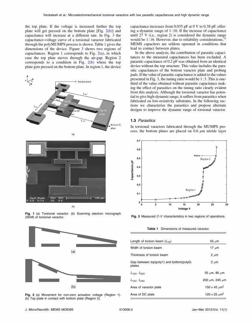
the top plate. If the voltage is increased further the topplate will get pressed on the bottom plate [Fig. 2(b)] andcapacitance will increase at a different rate. In Fig. 3 thecapacitance-voltage curve of a torsional varactor fabricatedthrough the polyMUMPS process is shown. Table 1 gives thedimensions of the device. Figure 3 shows two regions ofcapacitances. Region 1 corresponds to Fig. 2(a), in whichcase the top plate moves through the air-gap. Region 2corresponds to a condition in Fig. 2(b) where the topplate gets pressed on the bottom plate. In region 1, the device
capacitance increases from 0.035 pF at 0 V to 0.38 pF, offer-ing a dynamic range of 1∶10. If the increase of capacitanceuntil 27 V (i.e., region 2) is considered the dynamic rangewould be 1∶16. However, due to reliability considerations,14
MEMS capacitors are seldom operated in conditions thatlead to contact between plates.
In the above analysis, the contribution of parasitic capaci-tances to the measured capacitances has been excluded. Aparasitic capacitance of 0.2 pF was obtained from an identicaldevice without the top structure. This value includes the para-sitic capacitances of the bottom varactor plate and probingpads. If the value of parasitic capacitance is added to the valuespresented in Fig. 3, the tuning ratio would be 1∶3. This is one-third of the value obtained without parasitic capacitance mak-ing the effect of parasitics on the tuning ratio clearly evidentfrom this analysis. Although the torsional varactor has poten-tial to give high-dynamic range, it suffers from parasitics whenfabricated on low-resistivity substrates. In the following sec-tions we characterize the parasitics and propose alternatedesigns to improve the dynamic range of torsional varactor.
1.3 Parasitics
In torsional varactors fabricated through the MUMPS pro-cess, the bottom plates are placed on 0.6 μm nitride layer
Fig. 1 (a) Torsional varactor. (b) Scanning electron micrograph(SEM) of torsional varactor.
Fig. 2 (a) Movement for non-zero actuation voltage (Region 1).(b) Top plate in contact with bottom plate (Region 2).
0 5 10 15 20 25 300
0.1
0.2
0.3
0.4
0.5
0.6
0.7
Voltage V
Cap
acit
ance
pF
Pull-in
Region-1
Region-2
Fig. 3 Measured C-V characteristics in two regions of operations.
Table 1 Dimensions of measured varactor.
Length of torsion beam (LTB) 55 μm
Width of torsion beam 17 μm
Thickness of torsion beam 2 μm
Gap between top(poly1) and bottom(poly0)plates
2 μm
L1DC, L2DC 55 μm, 80 μm
L1AC, L2AC 200 μm, 245 μm
Area of varactor plate 150 × 45 μm2
Area of DC plate 120 × 25 μm2
Venkatesh et al.: Microelectromechanical torsional varactors with low parasitic capacitances and high dynamic range
J. Micro/Nanolith. MEMS MOEMS 013006-2 Jan–Mar 2012/Vol. 11(1)
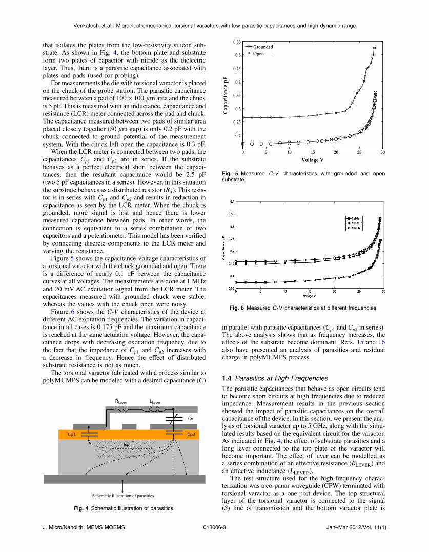
that isolates the plates from the low-resistivity silicon sub-strate. As shown in Fig. 4, the bottom plate and substrateform two plates of capacitor with nitride as the dielectriclayer. Thus, there is a parasitic capacitance associated withplates and pads (used for probing).
For measurements the die with torsional varactor is placedon the chuck of the probe station. The parasitic capacitancemeasured between a pad of 100 × 100 μm area and the chuckis 5 pF. This is measured with an inductance, capacitance andresistance (LCR) meter connected across the pad and chuck.The capacitance measured between two pads of similar areaplaced closely together (50 μm gap) is only 0.2 pF with thechuck connected to ground potential of the measurementsystem. With the chuck left open the capacitance is 0.3 pF.
When the LCR meter is connected between two pads, thecapacitances Cp1 and Cp2 are in series. If the substratebehaves as a perfect electrical short between the capaci-tances, then the resultant capacitance would be 2.5 pF(two 5 pF capacitances in a series). However, in this situationthe substrate behaves as a distributed resistor (Rd). This resis-tor is in series with Cp1 and Cp2 and results in reduction incapacitance as seen by the LCR meter. When the chuck isgrounded, more signal is lost and hence there is lowermeasured capacitance between pads. In other words, theconnection is equivalent to a series combination of twocapacitors and a potentiometer. This model has been verifiedby connecting discrete components to the LCR meter andvarying the resistance.
Figure 5 shows the capacitance-voltage characteristics ofa torsional varactor with the chuck grounded and open. Thereis a difference of nearly 0.1 pF between the capacitancecurves at all voltages. The measurements are done at 1 MHzand 20 mV AC excitation signal from the LCR meter. Thecapacitances measured with grounded chuck were stable,whereas the values with the chuck open were noisy.
Figure 6 shows the C-V characteristics of the device atdifferent AC excitation frequencies. The variation in capaci-tance in all cases is 0.175 pF and the maximum capacitanceis reached at the same actuation voltage. However, the capa-citance drops with decreasing excitation frequency, due tothe fact that the impedance of Cp1 and Cp2 increases witha decrease in frequency. Hence the effect of distributedsubstrate resistance is not as much.
The torsional varactor fabricated with a process similar topolyMUMPS can be modeled with a desired capacitance (C)
in parallel with parasitic capacitances (Cp1 and Cp2 in series).The above analysis shows that as frequency increases, theeffects of the substrate become dominant. Refs. 15 and 16also have presented an analysis of parasitics and residualcharge in polyMUMPS process.
1.4 Parasitics at High Frequencies
The parasitic capacitances that behave as open circuits tendto become short circuits at high frequencies due to reducedimpedance. Measurement results in the previous sectionshowed the impact of parasitic capacitances on the overallcapacitance of the device. In this section, we present the ana-lysis of torsional varactor up to 5 GHz, along with the simu-lated results based on the equivalent circuit for the varactor.As indicated in Fig. 4, the effect of substrate parasitics and along lever connected to the top plate of the varactor willbecome important. The effect of lever can be modelled asa series combination of an effective resistance (RLEVER) andan effective inductance (LLEVER).
The test structure used for the high-frequency charac-terization was a co-panar waveguide (CPW) terminated withtorsional varactor as a one-port device. The top structurallayer of the torsional varactor is connected to the signal(S) line of transmission and the bottom varactor plate isFig. 4 Schematic illustration of parasitics.
Fig. 5 Measured C-V characteristics with grounded and opensubstrate.
Fig. 6 Measured C-V characteristics at different frequencies.
Venkatesh et al.: Microelectromechanical torsional varactors with low parasitic capacitances and high dynamic range
J. Micro/Nanolith. MEMS MOEMS 013006-3 Jan–Mar 2012/Vol. 11(1)
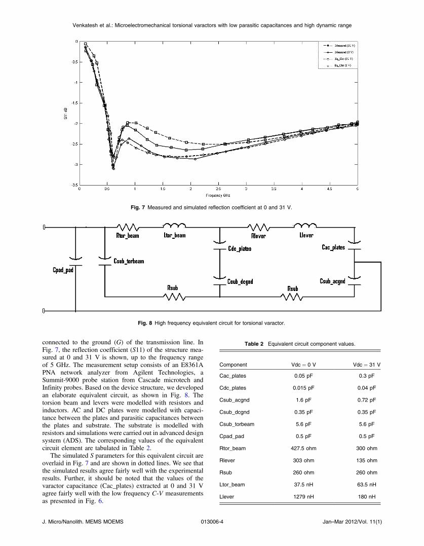
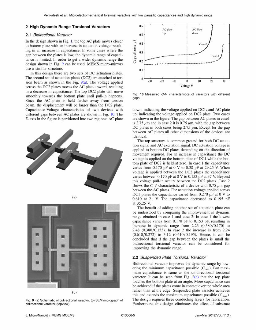
connected to the ground (G) of the transmission line. InFig. 7, the reflection coefficient (S11) of the structure mea-sured at 0 and 31 V is shown, up to the frequency rangeof 5 GHz. The measurement setup consists of an E8361APNA network analyzer from Agilent Technologies, aSummit-9000 probe station from Cascade microtech andInfinity probes. Based on the device structure, we developedan elaborate equivalent circuit, as shown in Fig. 8. Thetorsion beam and levers were modelled with resistors andinductors. AC and DC plates were modelled with capaci-tance between the plates and parasitic capacitances betweenthe plates and substrate. The substrate is modelled withresistors and simulations were carried out in advanced designsystem (ADS). The corresponding values of the equivalentcircuit element are tabulated in Table 2.
The simulated S parameters for this equivalent circuit areoverlaid in Fig. 7 and are shown in dotted lines. We see thatthe simulated results agree fairly well with the experimentalresults. Further, it should be noted that the values of thevaractor capacitance (Cac_plates) extracted at 0 and 31 Vagree fairly well with the low frequency C-V measurementsas presented in Fig. 6.
Fig. 7 Measured and simulated reflection coefficient at 0 and 31 V.
Fig. 8 High frequency equivalent circuit for torsional varactor.
Table 2 Equivalent circuit component values.
Component Vdc ¼ 0 V Vdc ¼ 31 V
Cac_plates 0.05 pF 0.3 pF
Cdc_plates 0.015 pF 0.04 pF
Csub_acgnd 1.6 pF 0.72 pF
Csub_dcgnd 0.35 pF 0.35 pF
Csub_torbeam 5.6 pF 5.6 pF
Cpad_pad 0.5 pF 0.5 pF
Rtor_beam 427.5 ohm 300 ohm
Rlever 303 ohm 135 ohm
Rsub 260 ohm 260 ohm
Ltor_beam 37.5 nH 63.5 nH
Llever 1279 nH 180 nH
Venkatesh et al.: Microelectromechanical torsional varactors with low parasitic capacitances and high dynamic range
J. Micro/Nanolith. MEMS MOEMS 013006-4 Jan–Mar 2012/Vol. 11(1)
2 High Dynamic Range Torsional Varactors
2.1 Bidirectional Varactor
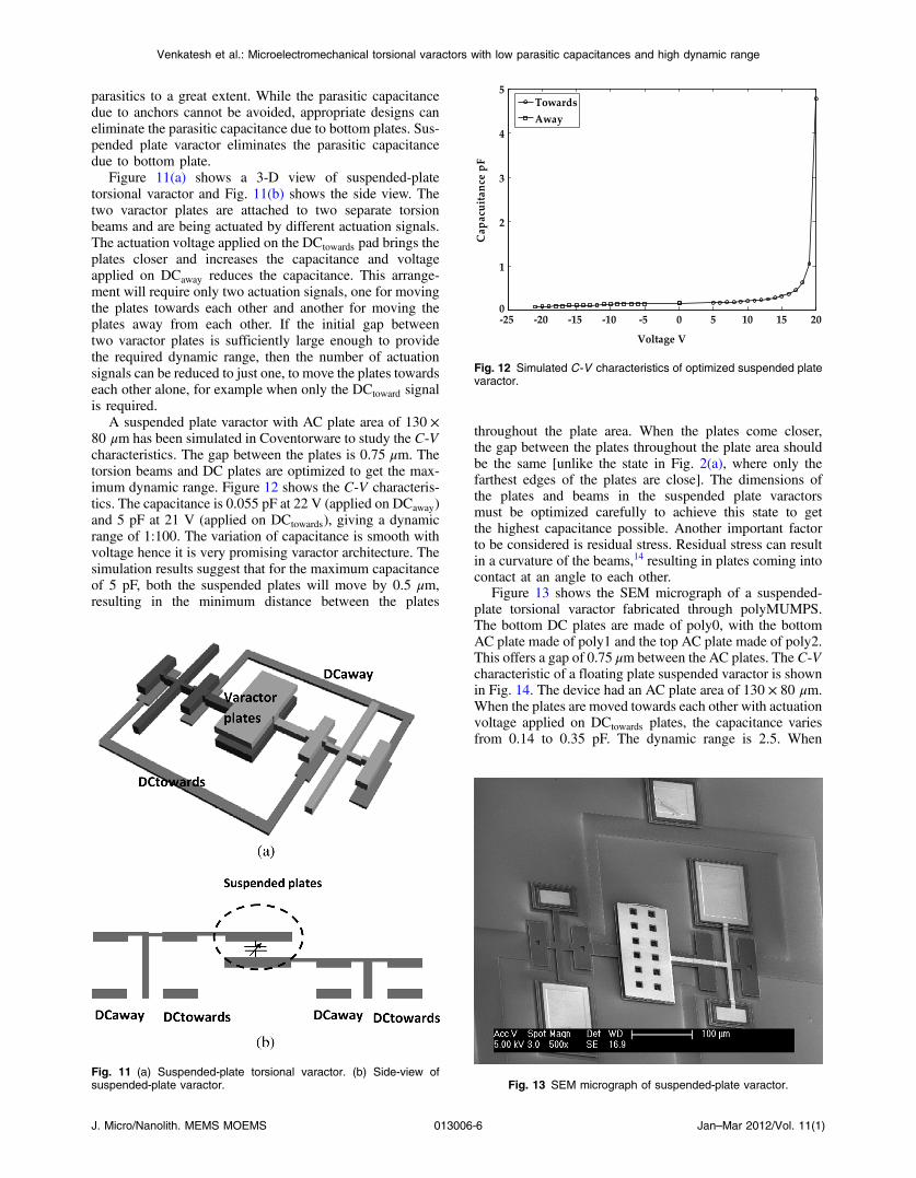
In the design shown in Fig. 1, the top AC plate moves closerto bottom plate with an increase in actuation voltage, result-ing in an increase in capacitance. In some cases where thegap between the plates is low, the dynamic range of capaci-tance is limited. In order to get a wider dynamic range thedesign shown in Fig. 9 can be used. MEMS micro-mirrorsuse a similar structure.
In this design there are two sets of DC actuation plates.The second set of actuation plates (DC2) are attached to tor-sion beam as shown in the Fig. 9(a). The voltage appliedacross the DC2 plates moves the AC plate upward, resultingin a decrease in capacitance. The top DC2 plate will movesmoothly towards the bottom plate until pull-in happens.Since the AC plate is held farther away from torsionbeam, the displacement will be larger than the DC2 plate.Capacitance-Voltage characteristics of two devices withdifferent gaps between AC plates are shown in Fig. 10. TheX-axis in the figure is partitioned into two regions: AC plate
down, indicating the voltage applied on DC1; and AC plateup, indicating the voltage applied on DC2 plate. Two casesare shown in the figure. The gap between AC plates in case1is 2.75 μm and in case 2 it is 0.75 μm, with the gap betweenDC plates in both cases being 2.75 μm. Except for the gapbetween AC plates all other dimensions of the devices areidentical.
The top structure is common ground for both DC actua-tion signal and AC excitation signal. DC actuation voltage isapplied to bottom DC plates depending on the direction ofmovement required. For an increase in capacitance the DCvoltage is applied on the bottom plate of DC1 while the bot-tom plate of DC2 is held at zero. In case 1 the capacitancevaries from 0.170 pF at 0 V to 0.38 pF at 29.25 V. Whenvoltage is applied between the DC2 plates the capacitancevaries between 0.170 pF at 0 V to 0.153 pF at 37 V. Beyondthis voltage pull-in occurs between the DC2 plates. Case 2shows the C-V characteristic of a device with 0.75 μm gapbetween the AC plates. For actuation voltage applied acrossDC1 plates the capacitance varied from 0.270 pF at 0 V to0.610 at 21 V. The capacitance decreased to 0.195 pFat 35.25 V.
The benefit of adding another set of actuation plate canbe understood by comparing the improvement in dynamicrange obtained in case 1 and case 2. In case 1 the lowestcapacitance varies from 0.170 pF to 0.153 pF, resulting inincrease in dynamic range from 2.23 (0.380∕0.170) to2.48 (0.380∕0.153). In case 2 the increase is from 2.24(0.610∕0.272) to 3.12 (0.610∕0.195). Hence, it can beconcluded that if the gap between the plates is small thebidirectional torsional varactor can be considered forimproving the dynamic range.
2.2 Suspended Plate Torsional Varactor
Bidirectional varactor improves the dynamic range by low-ering the minimum capacitance possible (Cmin). But maxi-mum capacitance is same as the unidirectional torsionalvaractor. It can be seen from Fig. 2(a) that the top platetouches the bottom plate at an angle. More capacitance canbe achieved if the plates come in contact over the whole arearather than at the edge. Suspended plate varactor achievesthis and extends the maximum capacitance possible (Cmax).The design requires three conducting layers for fabrication.Furthermore, this design eliminates the effect of substrate
Fig. 9 (a) Schematic of bidirectional varactor. (b) SEM micrograph ofbidirectional varactor (topview).
Fig. 10 Measured C-V characteristics of varactors with differentgaps.
Venkatesh et al.: Microelectromechanical torsional varactors with low parasitic capacitances and high dynamic range
J. Micro/Nanolith. MEMS MOEMS 013006-5 Jan–Mar 2012/Vol. 11(1)
parasitics to a great extent. While the parasitic capacitancedue to anchors cannot be avoided, appropriate designs caneliminate the parasitic capacitance due to bottom plates. Sus-pended plate varactor eliminates the parasitic capacitancedue to bottom plate.
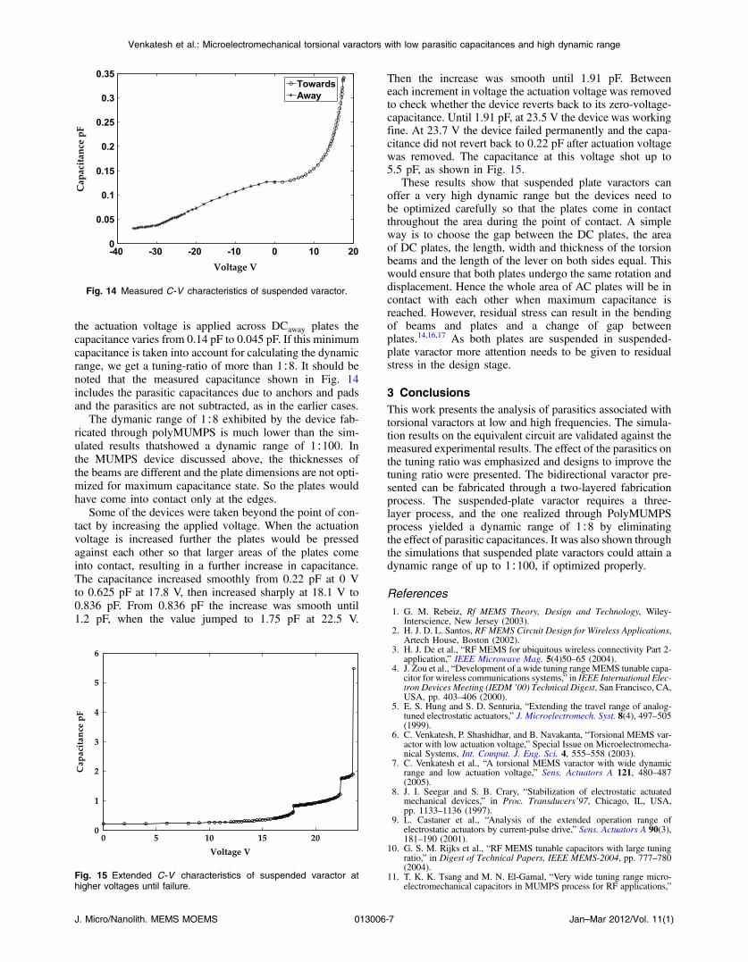
Figure 11(a) shows a 3-D view of suspended-platetorsional varactor and Fig. 11(b) shows the side view. Thetwo varactor plates are attached to two separate torsionbeams and are being actuated by different actuation signals.The actuation voltage applied on the DCtowards pad brings theplates closer and increases the capacitance and voltageapplied on DCaway reduces the capacitance. This arrange-ment will require only two actuation signals, one for movingthe plates towards each other and another for moving theplates away from each other. If the initial gap betweentwo varactor plates is sufficiently large enough to providethe required dynamic range, then the number of actuationsignals can be reduced to just one, to move the plates towardseach other alone, for example when only the DCtoward signalis required.
A suspended plate varactor with AC plate area of 130 ×80 μm has been simulated in Coventorware to study the C-Vcharacteristics. The gap between the plates is 0.75 μm. Thetorsion beams and DC plates are optimized to get the max-imum dynamic range. Figure 12 shows the C-V characteris-tics. The capacitance is 0.055 pF at 22 V (applied on DCaway)and 5 pF at 21 V (applied on DCtowards), giving a dynamicrange of 1:100. The variation of capacitance is smooth withvoltage hence it is very promising varactor architecture. Thesimulation results suggest that for the maximum capacitanceof 5 pF, both the suspended plates will move by 0.5 μm,resulting in the minimum distance between the plates
throughout the plate area. When the plates come closer,the gap between the plates throughout the plate area shouldbe the same [unlike the state in Fig. 2(a), where only thefarthest edges of the plates are close]. The dimensions ofthe plates and beams in the suspended plate varactorsmust be optimized carefully to achieve this state to getthe highest capacitance possible. Another important factorto be considered is residual stress. Residual stress can resultin a curvature of the beams,14 resulting in plates coming intocontact at an angle to each other.
Figure 13 shows the SEM micrograph of a suspended-plate torsional varactor fabricated through polyMUMPS.The bottom DC plates are made of poly0, with the bottomAC plate made of poly1 and the top AC plate made of poly2.This offers a gap of 0.75 μm between the AC plates. The C-Vcharacteristic of a floating plate suspended varactor is shownin Fig. 14. The device had an AC plate area of 130 × 80 μm.When the plates are moved towards each other with actuationvoltage applied on DCtowards plates, the capacitance variesfrom 0.14 to 0.35 pF. The dynamic range is 2.5. When
Fig. 11 (a) Suspended-plate torsional varactor. (b) Side-view ofsuspended-plate varactor.
Fig. 12 Simulated C-V characteristics of optimized suspended platevaractor.
Fig. 13 SEM micrograph of suspended-plate varactor.
Venkatesh et al.: Microelectromechanical torsional varactors with low parasitic capacitances and high dynamic range
J. Micro/Nanolith. MEMS MOEMS 013006-6 Jan–Mar 2012/Vol. 11(1)
the actuation voltage is applied across DCaway plates thecapacitance varies from 0.14 pF to 0.045 pF. If this minimumcapacitance is taken into account for calculating the dynamicrange, we get a tuning-ratio of more than 1∶8. It should benoted that the measured capacitance shown in Fig. 14includes the parasitic capacitances due to anchors and padsand the parasitics are not subtracted, as in the earlier cases.
The dymanic range of 1∶8 exhibited by the device fab-ricated through polyMUMPS is much lower than the sim-ulated results thatshowed a dynamic range of 1∶100. Inthe MUMPS device discussed above, the thicknesses ofthe beams are different and the plate dimensions are not opti-mized for maximum capacitance state. So the plates wouldhave come into contact only at the edges.
Some of the devices were taken beyond the point of con-tact by increasing the applied voltage. When the actuationvoltage is increased further the plates would be pressedagainst each other so that larger areas of the plates comeinto contact, resulting in a further increase in capacitance.The capacitance increased smoothly from 0.22 pF at 0 Vto 0.625 pF at 17.8 V, then increased sharply at 18.1 V to0.836 pF. From 0.836 pF the increase was smooth until1.2 pF, when the value jumped to 1.75 pF at 22.5 V.
Then the increase was smooth until 1.91 pF. Betweeneach increment in voltage the actuation voltage was removedto check whether the device reverts back to its zero-voltage-capacitance. Until 1.91 pF, at 23.5 V the device was workingfine. At 23.7 V the device failed permanently and the capa-citance did not revert back to 0.22 pF after actuation voltagewas removed. The capacitance at this voltage shot up to5.5 pF, as shown in Fig. 15.
These results show that suspended plate varactors canoffer a very high dynamic range but the devices need tobe optimized carefully so that the plates come in contactthroughout the area during the point of contact. A simpleway is to choose the gap between the DC plates, the areaof DC plates, the length, width and thickness of the torsionbeams and the length of the lever on both sides equal. Thiswould ensure that both plates undergo the same rotation anddisplacement. Hence the whole area of AC plates will be incontact with each other when maximum capacitance isreached. However, residual stress can result in the bendingof beams and plates and a change of gap betweenplates.14,16,17 As both plates are suspended in suspended-plate varactor more attention needs to be given to residualstress in the design stage.
3 ConclusionsThis work presents the analysis of parasitics associated withtorsional varactors at low and high frequencies. The simula-tion results on the equivalent circuit are validated against themeasured experimental results. The effect of the parasitics onthe tuning ratio was emphasized and designs to improve thetuning ratio were presented. The bidirectional varactor pre-sented can be fabricated through a two-layered fabricationprocess. The suspended-plate varactor requires a three-layer process, and the one realized through PolyMUMPSprocess yielded a dynamic range of 1∶8 by eliminatingthe effect of parasitic capacitances. It was also shown throughthe simulations that suspended plate varactors could attain adynamic range of up to 1∶100, if optimized properly.
References
1. G. M. Rebeiz, Rf MEMS Theory, Design and Technology, Wiley-Interscience, New Jersey (2003).
2. H. J. D. L. Santos, RF MEMS Circuit Design for Wireless Applications,Artech House, Boston (2002).
3. H. J. De et al., “RF MEMS for ubiquitous wireless connectivity Part 2-application,” IEEE Microwave Mag. 5(4)50–65 (2004).
4. J. Zou et al., “Development of a wide tuning rangeMEMS tunable capa-citor for wireless communications systems,” in IEEE International Elec-tron Devices Meeting (IEDM ’00) Technical Digest, San Francisco, CA,USA, pp. 403–406 (2000).
5. E. S. Hung and S. D. Senturia, “Extending the travel range of analog-tuned electrostatic actuators,” J. Microelectromech. Syst. 8(4), 497–505(1999).
6. C. Venkatesh, P. Shashidhar, and B. Navakanta, “Torsional MEMS var-actor with low actuation voltage,” Special Issue on Microelectromecha-nical Systems, Int. Comput. J. Eng. Sci. 4, 555–558 (2003).
7. C. Venkatesh et al., “A torsional MEMS varactor with wide dynamicrange and low actuation voltage,” Sens. Actuators A 121, 480–487(2005).
8. J. I. Seegar and S. B. Crary, “Stabilization of electrostatic actuatedmechanical devices,” in Proc. Transducers’97, Chicago, IL, USA,pp. 1133–1136 (1997).
9. L. Castaner et al., “Analysis of the extended operation range ofelectrostatic actuators by current-pulse drive,” Sens. Actuators A 90(3),181–190 (2001).
10. G. S. M. Rijks et al., “RF MEMS tunable capacitors with large tuningratio,” in Digest of Technical Papers, IEEE MEMS-2004, pp. 777–780(2004).
11. T. K. K. Tsang and M. N. El-Gamal, “Very wide tuning range micro-electromechanical capacitors in MUMPS process for RF applications,”
Fig. 14 Measured C-V characteristics of suspended varactor.
Fig. 15 Extended C-V characteristics of suspended varactor athigher voltages until failure.
Venkatesh et al.: Microelectromechanical torsional varactors with low parasitic capacitances and high dynamic range
J. Micro/Nanolith. MEMS MOEMS 013006-7 Jan–Mar 2012/Vol. 11(1)
Digest of Technical Papers, Symposium on VLSI circuits, pp. 33–36(2003).
12. M. Bakri-Kassem and R. R. Mansour, “Linear bilayer ALD coatedMEMS varactor with high tuning capacitance ratio,” J. Microelectro-mech. Syst. 18(1), 147–153 (2009).
13. D.A. Koester et al., ”MUMPS Design Handbook,” Revision 5.0,Cronos Integrated Microsystems, Research Triangle Park, NC (2000).
14. C. Venkatesh and N. Bhat, “Reliability analysis of torsional MEMSvaractor,” IEEE Trans. Device Mater. Reliab. 8(1), 129–134(2008).
15. E. K. Chan and R. W. Dutton, “Effects of capacitors, resistors and resi-dual charge on the static and dynamic performance of electrostaticallyactuated devices,” Proc. SPIE 3680, 120–130 (1999).
16. A. M. Elshurafa and E. I. El-Masry, “Design considerations in MEMSparallel plate variable capacitors,” in Proc. MWSCAS-2007, Montreal,Quebec, pp. 1173–1176 (Aug 2007).
17. A. Dec and K. Suyama, “Micromachined electro-mechanically tunablecapacitors and their applications to RF ICs,” IEEE Trans. MicrowaveTheor. Tech. 46(12), 2587–2596 (1998).
Chenniappan Venkatesh received his BE ininstrumentation and control from the NationalInstitute of Technology, Trichy in 1998, MSc(engineering) from the Indian Institute ofScience in 2001 and PhD from Indian Insti-tute of Science in 2008. From 2008 to2010 he was with the University of Newcas-tle, Australia as a post-doctoral fellow. At pre-sent he is at the University of WesternAustralia as post-doctoral researcher. Hisresearch interests include MEMS, systems
dynamics and control and photonics.
Navakanta Bhat received his BE in electro-nics and communication from the Universityof Mysore in 1989, MTech in microelectronicsfrom I.I.T. Bombay in 1992 and PhD in elec-trical engineering from Stanford University,Stanford, CA in 1996. Then he worked atMotorola’s Networking and Computing Sys-tems Group in Austin, TX until 1999. AtMotorola he worked on logic technologydevelopment, and he was responsible fordeveloping high-performance transistor
design and dual gate oxide technology. He joined the Indian Instituteof Science, Bangalore in 1999 where he is currently a professor in theCentre for Nano Science and Engineering and Electrical Communica-tion Engineering department. His current research is focused Nano-CMOS technology and Integrated CMOS-MEMS sensors. The workspans the domains of process technology, device design, circuitdesign and modeling. He has 150 research publications in interna-tional journals and conferences and five U.S. patents.
K. J. Vinoy is an associate professor in theDepartment of Electrical CommunicationEngineering at the Indian Institute of Science(IISc), Bangalore, since 2003. He receivedBTech from the University of Kerala,MTech from Cochin University of Scienceand Technology, India, and PhD from thePennsylvania State University, USA, in1990, 1993, and 2002, respectively. From1994 to 1998 he worked at National Aero-space Laboratories, Bangalore, India. From
1999 to 2002, he worked as a research assistant and from 2002 toAugust 2003 as a Postdoctoral fellow at the Pennsylvania State Uni-versity. His research interests include several aspects of microwaveengineering such as fractal antennas, wideband antennas, passivecircuits, RF-MEMS and Computational Electromagnetics. He haspublished over 130 papers and four books. He has one US Patentawarded and three Indian patents filed. He is in the editorial boardsof three journals. He is a fellow of the Indian National Academy ofEngineering.
Satish Grandhi received his BE in electro-nics and communication engineering (ECE)from Andhra University, Vishakapatnam,India in 2005 and his MTech in microelectro-nics fromNITK Surathkal, Mangalore, India in2007. He is currently working as a seniorelectrical design engineer with CypressSemiconductor, Bangalore, India.
Venkatesh et al.: Microelectromechanical torsional varactors with low parasitic capacitances and high dynamic range
J. Micro/Nanolith. MEMS MOEMS 013006-8 Jan–Mar 2012/Vol. 11(1)