microdxp technical reference manual - xia...information furnished by xia llc is believed to be...
TRANSCRIPT

microDXP Technical Reference Manual
Version 3.14 January 12, 2016
microDXP Hardware Revision: H (8)
ProSpect Software Software Revision: 1.0.24
XIA LLC
31057 Genstar Rd Hayward, CA 94544 USA Email: [email protected]
Tel: (510) 401-5760; Fax: (510) 401-5761 http://www.xia.com/
Information furnished by XIA LLC is believed to be accurate and reliable. However, no responsibility is assumed by XIA for its use, or for any infringements of patents or other rights of third parties which may result from its use. No license is granted by implication or otherwise under any patent or patent rights of XIA. XIA reserves the right to change hardware or software specifications at any time without notice.
microDXP Technical Reference Manual Version 3.13
January 12, 2016 2
Table of Contents
Safety .............................................................................................................................................. 7
Specific Precautions .................................................................................................................................. 7
Power Source ........................................................................................................................................ 7
Detector and Preamplifier Damage ....................................................................................................... 7
Servicing and Cleaning ......................................................................................................................... 7
Warranty Statement ..................................................................................................................... 8
Contact Information: ................................................................................................................................. 8
Manual Conventions ..................................................................................................................... 9
1 Introduction ......................................................................................................................... 10
1.1 Features ....................................................................................................................................... 10
1.1.1 General Spectrometer Features ........................................................................................... 10
1.1.2 Embedded Systems Features ............................................................................................... 11
1.1.3 Custom OEM Features ........................................................................................................ 11
1.2 Hardware Requirements .............................................................................................................. 11
1.2.1 Host Computer .................................................................................................................... 11
1.2.2 Detector/Preamplifier .......................................................................................................... 11
1.2.3 Power Requirements ........................................................................................................... 12
1.2.4 Operating Environment ....................................................................................................... 12
1.2.5 Regulatory Compliance ....................................................................................................... 12
1.3 Hardware Options ....................................................................................................................... 12
1.3.1 Communications and Power Interface ................................................................................ 12
1.3.2 Analog Input ....................................................................................................................... 13
1.3.3 Power Supplies .................................................................................................................... 13
1.3.4 Pipeline Clock Speed Choice .............................................................................................. 14
1.3.5 Gain and Calibration Options ............................................................................................. 14
1.4 Firmware Options ....................................................................................................................... 14
1.4.1 Preamplifier Type ............................................................................................................... 14
1.4.2 Custom Firmware ................................................................................................................ 15
1.5 Application Examples ................................................................................................................. 15
1.5.1 Example 1. General-Purpose USB Spectrometer with MicroComU Companion Board .... 15
1.5.2 Example 2. General-Purpose Spectrometer Using RS232 and Custom Breakout Board ... 16
1.5.3 Example 3. Dedicated Spectrometer Using RS232 ............................................................. 16

microDXP Technical Reference Manual Version 3.13
January 12, 2016 3
1.6 Software Overview ..................................................................................................................... 18
1.6.1 User Interface, e.g. ProSpect ............................................................................................... 18
1.6.2 Device Drivers, e.g. Handel ................................................................................................ 18
1.6.3 Firmware ............................................................................................................................. 19
1.7 Support ........................................................................................................................................ 19
1.7.1 Software and Firmware Updates ......................................................................................... 19
1.7.2 XUP Utility and Firmware Updates .................................................................................... 19
1.7.3 Related Documentation ....................................................................................................... 19
1.7.4 Email and Phone Support .................................................................................................... 20
1.7.4.1 Submitting a problem report: .......................................................................................... 20
1.7.5 Feedback ............................................................................................................................. 21
1.7.5.1 Export File Formats ........................................................................................................ 21
2 Using the microDXP ............................................................................................................ 22
2.1 Hardware Settings ....................................................................................................................... 22
2.1.1 Preamplifier Type Selection ................................................................................................ 22
2.1.2 Input Signal Attenuation ..................................................................................................... 22
2.2 Board State and Configuration .................................................................................................... 23
2.2.1 Board Information and Status ............................................................................................. 23
2.2.1.1 ADC Sampling Rate / DSP Clock Speed: DSPSPEED .................................................. 23
2.2.1.2 Gain Mode ...................................................................................................................... 23
2.2.2 Serial Number ..................................................................................................................... 24
2.2.3 On-Board Temperature ....................................................................................................... 24
2.3 Global Settings and the GLOBSET ............................................................................................ 24
2.3.1 Preamplifier Settings ........................................................................................................... 24
2.3.1.1 Preamplifier Type ........................................................................................................... 24
2.3.1.2 Decay Time: TAURC ..................................................................................................... 25
2.3.1.3 Reset Interval: RESETINT ............................................................................................. 25
2.3.1.4 Preamplifier Signal Polarity ............................................................................................ 25
2.3.2 Advanced Processor Settings .............................................................................................. 25
2.4 MCA Settings and GENSETs ..................................................................................................... 26
2.4.1 Selecting the GENSET ........................................................................................................ 26
2.4.2 MCA Size and Bin Width ................................................................................................... 26
2.4.3 Base Gain, Switched Gain and Digital Base Gain .............................................................. 27

microDXP Technical Reference Manual Version 3.13
January 12, 2016 4
2.4.4 Reading the Current GENSET ............................................................................................ 28
2.4.5 Saving the Current GENSET to Non-Volatile Memory ..................................................... 28
2.5 Spectrometer Settings and PARSETs ......................................................................................... 28
2.5.1 Selecting a PARSET ........................................................................................................... 28
2.5.2 Thresholds ........................................................................................................................... 28
2.5.3 Baseline Average Length .................................................................................................... 29
2.5.4 Fine Gain Trim .................................................................................................................... 29
2.5.5 Advanced Filter Settings ..................................................................................................... 30
2.5.6 Reading the Current PARSET ............................................................................................ 30
2.5.7 Saving the Current PARSET to Non-Volatile Memory ...................................................... 30
2.6 Repetitive Configuration of Identical Systems ........................................................................... 30
2.6.1 Create Master Parameter Set… ........................................................................................... 30
2.6.2 Download a Master Parameter Set… .................................................................................. 30
2.7 Data Acquisition ......................................................................................................................... 30
2.7.1 Starting a Run ..................................................................................................................... 31
2.7.2 Stopping a Run .................................................................................................................... 31
2.7.3 Reading a Spectrum ............................................................................................................ 31
2.7.4 Reading (and Calculating) the Run Statistics ...................................................................... 31
2.7.5 Specifying fixed run lengths ............................................................................................... 32
2.8 Diagnostic Tools ......................................................................................................................... 32
2.8.1 Diagnostic Trace ................................................................................................................. 32
2.8.1.1 Trace Type (TRACETYPE) ............................................................................................ 33
2.8.1.2 Sampling Interval (TRACEWAIT) ................................................................................. 33
2.8.1.3 Trigger Type (TRACETRIG) ......................................................................................... 34
2.8.1.4 Pre-Trigger Position (TRACEPRETRIG)....................................................................... 34
2.8.2 Baseline Histogram ............................................................................................................. 35
2.8.3 DSP Parameters................................................................................................................... 35
3 MicroDXP Functional Description .................................................................................... 36
3.1 Organizational Overview ............................................................................................................ 36
3.2 The Analog Signal Conditioner (ASC) ....................................................................................... 36
3.2.1 Dynamic Range Reduction ................................................................................................. 37
3.2.1.1 Reset-Type Preamplifiers ................................................................................................ 37
3.2.1.2 RC-Feedback Preamplifiers ............................................................................................ 38

microDXP Technical Reference Manual Version 3.13
January 12, 2016 5
3.2.2 Analog Gain ........................................................................................................................ 39
3.2.2.1 Nominal Gain .................................................................................................................. 40
3.2.2.2 Switched Gain ................................................................................................................. 40
3.2.3 Nyquist Criterion................................................................................................................. 41
3.3 The Analog to Digital Converter (ADC) .................................................................................... 41
3.4 The Filter, Pulse Detector, & Pile-up Inspector (FiPPI) ............................................................. 41
3.4.1 Clock Speed and Peaking Time Range ............................................................................... 41
3.4.2 FiPPI Variants ..................................................................................................................... 42
3.4.3 Digital Gain ......................................................................................................................... 42
3.4.3.1 Digital Base Gain ............................................................................................................ 42
3.4.3.2 MCA Bin Width .............................................................................................................. 43
3.4.3.3 Fine Gain Trim ................................................................................................................ 43
3.5 The Digital Signal Processor (DSP ............................................................................................. 43
3.5.1 Parallel Flash EEPROM ...................................................................................................... 44
3.5.2 Serial Port (SPORT)............................................................................................................ 44
3.5.3 DMA Port ............................................................................................................................ 44
3.5.4 DSP Code Variants ............................................................................................................. 44
3.6 PIC Microcontroller .................................................................................................................... 44
3.6.1 RS-232 Serial Port .............................................................................................................. 45
3.6.2 I2C Serial Bus ..................................................................................................................... 45
3.6.3 I2C EEPROM ..................................................................................................................... 45
3.6.4 I2C Temperature Sensor ..................................................................................................... 45
3.6.5 PIC Code Variants .............................................................................................................. 45
3.7 Interface to Host Computer ......................................................................................................... 45
3.7.1 On-Board mini-USB 2.0 ..................................................................................................... 45
3.7.2 Flex Cable Interface ............................................................................................................ 45
3.7.3 Board-to-Board Interface .................................................................................................... 46
4 Digital Filtering: Theory of Operation and Implementation Methods .......................... 47
4.1 X-ray Detection and Preamplifier Operation .............................................................................. 47
4.1.1 Reset-Type Preamplifiers .................................................................................................... 47
4.1.2 RC-Type Preamplifiers ....................................................................................................... 49
4.2 X-ray Energy Measurement & Noise Filtering ........................................................................... 49
4.3 Trapezoidal Filtering in the DXP ................................................................................................ 51
4.4 Baseline Issues ............................................................................................................................ 53

microDXP Technical Reference Manual Version 3.13
January 12, 2016 6
4.4.1 The Need for Baseline Averaging ....................................................................................... 53
4.4.2 Raw Baseline Measurement ................................................................................................ 54
4.4.3 Baseline Averaging in the DXP .......................................................................................... 54
4.5 X-ray Detection & Setting Thresholds ........................................................................................ 55
4.6 Peak Capture Methods ................................................................................................................ 56
4.6.1 The Slow Filter Gap Length ................................................................................................ 56
4.6.2 Peak Sampling vs. Peak Sensing ......................................................................................... 57
4.7 Pile-up Inspection ....................................................................................................................... 58
4.7.1 Slow Pileup ......................................................................................................................... 59
4.7.2 Fast Pileup ........................................................................................................................... 60
4.8 Input Count Rate (ICR) and Output Count Rate (OCR) ............................................................. 61
4.9 Throughput .................................................................................................................................. 61
Appendices ................................................................................................................................... 63
Appendix A. MicroDXP Hardware Specification .................................................................................. 63
A.1 Board Dimensions and Mounting ................................................................................................ 63
A.2 Preamplifier Type Selector Switch .............................................................................................. 63
A.3 Input Signal Attenuation .............................................................................................................. 63
A.4 Connector Locations and Pinouts ................................................................................................. 63
A.5 Power Supplies ............................................................................................................................. 68
Appendix B. GLOBSET Specification ................................................................................................... 68
Appendix C. GENSET Specification ...................................................................................................... 69
Appendix D. PARSET Specification ...................................................................................................... 70
Appendix E. RS-232 Communications ................................................................................................... 71
microDXP Technical Reference Manual Version 3.13
January 12, 2016 7
Safety
Please take a moment to review these safety precautions. They are provided both for your protection and to prevent damage to the microDXP module and connected equipment. This safety information applies to all operators and service personnel.
Specific Precautions
Please take a moment to review these safety precautions. They are provided to prevent damage to the microDXP and microCOMU printed circuit boards and connected equipment. This safety information applies to all operators and service personnel.
Power Source The microDXP USB Rapid Development Kit includes a wall-mounted power supply intended to operate from an AC power supply in the 100VAC to 240VAC range at 50Hz or 60Hz. Use of this development kit with AC voltage outside these specifications could damage the unit and nullify the product warranty. Refer to Chapter 2 of this manual for instructions on installing the power supply.
Detector and Preamplifier Damage Because the microDXP does not provide power for the detector or preamplifier there is little risk of damage to either resulting from the microDXP itself. Nonetheless, please review all instructions and safety precautions provided with these components before powering a connected system.
Servicing and Cleaning To avoid personal injury, and/or damage to the microDXP and microCOMU boards or connected equipment, do not attempt to repair or clean these units. These boards are warranted against all defects for one (1) year. Please contact the factory or your distributor before returning items for service.

microDXP Technical Reference Manual Version 3.13
January 12, 2016 8
Warranty Statement
XIA LLC warrants that this product will be free from defects in materials and workmanship for a period of one (1) year from the date of shipment. If any such product proves defective during this warranty period, XIA LLC, at its option, will either repair the defective products without charge for parts and labor, or will provide a replacement in exchange for the defective product.
In order to obtain service under this warranty, Customer must notify XIA LLC of the defect before the expiration of the warranty period and make suitable arrangements for the performance of the service.
This warranty shall not apply to any defect, failure or damage caused by improper uses or inadequate care. XIA LLC shall not be obligated to furnish service under this warranty a) to repair damage resulting from attempts by personnel other than XIA LLC representatives to repair or service the product; or b) to repair damage resulting from improper use or connection to incompatible equipment.
THIS WARRANTY IS GIVEN BY XIA LLC WITH RESPECT TO THIS PRODUCT IN LIEU OF ANY OTHER WARRANTIES, EXPRESSED OR IMPLIED. XIA LLC AND ITS VENDORS DISCLAIM ANY IMPLIED WARRANTIES OF MERCHANTABILITYOR FITNESS FOR A PARTICULAR PURPOSE. XIA’S RESPONSIBILITY TO REPAIR OR REPLACE DEFECTIVE PRODUCTS IS THE SOLE AND EXCLUSIVE REMEDY PROVIDED TO THE CUSTOMER FOR BREACH OF THIS WARRANTY. XIA LLC AND ITS VENDORS WILL NOT BE LIABLE FOR ANY INDIRECT, SPECIAL, INCIDENTAL, OR CONSEQUENTIAL DAMAGES IRRESPECTIVE OF WHETHER XIA LLC OR THE VENDOR HAS ADVANCE NOTICE OF THE POSSIBILITY OF SUCH DAMAGES.
Contact Information:
XIA LLC
31057 Genstar Rd.
Hayward, CA 94544 USA
Telephone: (510) 401-5760
Downloads: http://support.xia.com
Email Support: [email protected]
microDXP Technical Reference Manual Version 3.13
January 12, 2016 9
Manual Conventions
The following conventions are used throughout this manual
Convention Description Example » The » symbol leads you
through nested menu items and dialog box options.
The sequence File»Page Setup»Options directs you to pull down the File menu, select the Page Setup item, and choose Options from the sub menu.
Bold Bold text denotes items that you must select or click on in the software, such as menu items, and dialog box options.
...click on the MCA tab.
[Bold] Bold text within [ ] denotes a command button.
[Start Run] indicates the command button labeled Start Run.
monospace Items in this font denote text or characters that you enter from the keyboard, sections of code, file contents, and syntax examples.
Setup.exe refers to a file called “setup.exe” on the host computer.
Italics Italic text denotes a new term being introduced , or simply emphasis
peaking time refers to the length of the slow filter. ...it is important first to set the energy filter Gap so that SLOWGAP to at least one unit greater than the preamplifier rise time...
<Key> <Shift-Alt-Delete> or <Ctrl+D>
Angle brackets denote a key on the keyboard (not case sensitive). A hyphen or plus between two or more key names denotes that the keys should be pressed simultaneously (not case sensitive).
<W> indicates the W key <Ctrl+W> represents holding the control key while pressing the W key on the keyboard
Bold italic Warnings and cautionary text. CAUTION: Improper connections or settings can result in damage to system components.
CAPITALS CAPITALS denote DSP parameter names
SLOWLEN is the length of the slow energy filter

microDXP Technical Reference Manual Version 3.13
January 12, 2016 10
1 Introduction
The Micro Digital X-ray Processor (microDXP) is a high rate, digitally-based, multi-channel analysis spectrometer designed for energy dispersive x-ray or gamma-ray measurements in benchtop, networked, portable and embedded systems. Its versatile analog front-end accommodates most solid-state and gas detectors and a wide range of common preamplifiers, including pulsed optical reset, transistor reset, and resistive feedback types. The microDXP offers complete computer control over all available amplifier and spectrometer controls including gain (if applicable), filter peaking time, and pileup inspection criteria. As with all DXP instruments, the firmware (i.e. DSP, Microcontroller and FPGA code) can be upgraded in the field. Unlike other instruments in the DXP family, microDXP firmware and parameters are stored locally in non-volatile memory.
The architecture supports custom auxiliary digital access including the industry-standard I2C serial bus and four configurable digital I/O lines. The microDXP is thus a flexible, cost-effective OEM component that can form the core of a broad range of systems, from basic XRF to the most demanding process and control applications emerging in research and industry.
This version of the manual describes the new ‘blue’ microDXP pictured on the right below. If your microDXP is green, as pictured on the left, please refer to the older version 1.0.2 of this manual.
Figure 1-1: The new microDXP pictured on the right was released in 2015.
1.1 Features
The microDXP offers a set of standard and customizable features intended to address the design requirements of a wide range of complex spectroscopy data acquisition systems.
1.1.1 General Spectrometer Features • Extremely compact unit replaces spectroscopy amplifier, shaping amplifier and
multi-channel analyzer (MCA) at significantly reduced cost and power consumption. • Operates with a wide variety of x-ray or gamma-ray detectors using preamplifiers of
pulsed optical reset, transistor reset or resistor feedback types.
microDXP Technical Reference Manual Version 3.13
January 12, 2016 11
• Multi-channel analysis with up to 8K (8192) bins, allowing for optimal use of data to separate fluorescence signal from backgrounds.
• Instantaneous throughput beyond 1,000,000 counts per second (cps) into the spectrum for the standard 40MHz ADC clock speed.
• Digital trapezoidal filtering, with programmable peaking times between 100 ns and 24 µs for the standard 40MHz ADC clock speed.
• Digitally-controlled analog gain: 25.5 dB range, 16 discrete settings. • Digital fine gain trim: 16-bit precision • Pileup inspection criteria computer settable, including fast channel peaking time,
threshold, and rejection criterion. • Accurate ICR and live-time reporting for precise dead-time corrections.
1.1.2 Embedded Systems Features
• Data acquisition and control via RS-232 or USB. • Twenty-four (24) sets of optimized spectrometer parameters, or PARSETs, are stored
and retrieved on a per-peaking-time basis in nonvolatile memory. • Five (5) sets of MCA parameters, or GENSETs, are stored and retrieved in
nonvolatile memory. • XIA provides the ProSpect software application for microDXP parameter set
configuration—intended for use both in evaluation and production phases.
1.1.3 Custom OEM Features • Customized firmware development for special applications such as time-resolved
spectroscopy, multiple SCA’s and pulse-shape analysis. • Flexible auxiliary digital I/O: 4 general purpose lines, a Gate signal to externally
control data acquisition, I2C bus interface and an external interrupt line. • Assembly options are offered to exclude various hardware and software features in
order to reduce the cost for dedicated applications (further details in the following section).
1.2 Hardware Requirements
1.2.1 Host Computer The microDXP can communicate with any host computer/controller via RS-232. Windows 7 or later is required to operate via USB.
1.2.2 Detector/Preamplifier The microDXP accommodates nearly all detector preamplifier signals. The two primary capacitor-discharge topologies, pulsed-reset and resistive-feedback, are supported. The voltage compliance range in the DXP analog circuitry imposes the following constraints:
Parameter Minimum Maximum* X-ray pulse-height 50 µV 125 mV Input voltage range - +/- 4.0 V Decay time τ 100 ns 8.19 ms
Table 1-1: Analog input signal constraints

microDXP Technical Reference Manual Version 3.13
January 12, 2016 12
*The microDXP input circuitry is configured by default for typical x-ray and gamma-ray detector gain values. Larger pulse-heights and input voltage range are accommodated via input signal attenuation (see §2.1.2 and Appendix A for details).
1.2.3 Power Requirements The microDXP consumes approximately 750 mW. The onboard digital circuitry draws from a 3.3 V input, while analog circuitry runs from +/-5.0 V, either supplied directly or indirectly through on-board LDO regulators. Full power supply specifications are included in Appendix A.
1.2.4 Operating Environment Temperature Range: 0° C - 50° C
Maximum Relative Humidity: 75%, non-condensing.
Maximum Altitude: 3,000 meters
Pollution degree 2
Not rated for use in high electromagnetic fields.
Not rated for use in environments with measurable neutron flux. Neutron flux will cause permanent damage to silicon crystals and permanently degrade or impair the performance of this system.
The components on the microDXP board are not radiation hardened. Although there should not be a problem operating them in environments with modest gamma or X-ray flux, above a certain level this radiation will start to cause bit errors in the digital components. If necessary, please contact XIA LLC to discuss a proposed radiation environment.
1.2.5 Regulatory Compliance The microDXP board is RoHS compliant.
1.3 Hardware Options
The microDXP hardware is both powerful and flexible. XIA is pleased to offer a number of assembly options that will produce the best value for a given set of requirements. The specification sheet provided with your microDXP lists the options that have been implemented. Note: The preamplifier type and auxiliary digital I/O options can typically be upgraded in the field, whereas the ADC speed, power supply and gain options require physical modifications to the hardware. Please contact XIA for more information about hardware options and upgrades:
1.3.1 Communications and Power Interface Power, communications and auxiliary digital I/O is redundantly accessible on two separate connectors: a flat-flex cable for low and medium speed serial communications and a board-to-board connector that offers serial protocols as well as high-speed parallel access.
The flex-cable interconnect supports RS-232 at up to 921 kbaud, with burst rates up to 10 Kbytes/sec, and Analog Devices DSP serial port (SPORT) communications for faster data

microDXP Technical Reference Manual Version 3.13
January 12, 2016 13
transfers, up to 2 Mbytes/sec. The SPORT option is targeted for multi-channel systems and will require some user hardware and DSP code development.
The board-to-board connector supports RS-232 and SPORT serial communications, as well as parallel IDMA access to DSP memory for transfer rates up to 10 Mbytes/sec. This parallel IDMA interface is used as the basis for the MicroComU USB interface.
The latest microDXP hardware includes an optional on-board USB interface, simplifying the implementation design process for embedded systems. With this option, the customer need only provide power and auxiliary digital I/O connections via the flat-flex cable or board-to-board connector.
1.3.2 Analog Input The analog input signal enters via a separate connector to ensure immunity from electro-magnetic interference. Twisted-pair, coaxial and board-to-board connections are supported. See Appendix A for more information.
1.3.3 Power Supplies Two power supply variants are available, corresponding to whether on-board regulators for the analog supply voltages are used or are bypassed. If +/-5.0 V is supplied directly, either linear regulated or high-quality switching supplies should be used. If the on-board LDO regulators are used a minimum of +/-5.50 V is required, and the ripple requirement can be relaxed a bit.
If planning to use the MicroComU companion board, choose the variant of the microDXP that includes on-board voltage regulators. Aside from this, the MicroComU board will take care of generating all required voltages for the microDXP, at the specified currents and noise performance.
Regulated Supply Option: (<20mV pk-pk noise)
Voltage Range Current (min) Current (max) Description +3.3V +/- 150mV 150mA 200mA Decent switching supply +5.0V +/- 100mV 25mA 30mA Linear or high-quality
switching -5.0V +/- 100mV 25mA 30mA Linear or high-quality
switching Unregulated Supply Option: (<100mV pk-pk noise)
Voltage Range Current (min) Current (max) Description +3.3V +/- 150mV 150mA 200mA Decent switching supply +5.5V to +6.0V 25mA 35mA Decent switching supply -5.5V to –6.0V 25mA 35mA Decent switching supply
Table 1-2: Power supply options and specifications for the microDXP.
For both variants, the onboard digital circuitry draws from a 3.3V supply input. The ripple requirements for this supply are not particularly stringent, though excessive radiated noise is to be avoided. If a switching supply is used, it should be well shielded from, and properly grounded with respect to, the microDXP.
microDXP Technical Reference Manual Version 3.13
January 12, 2016 14
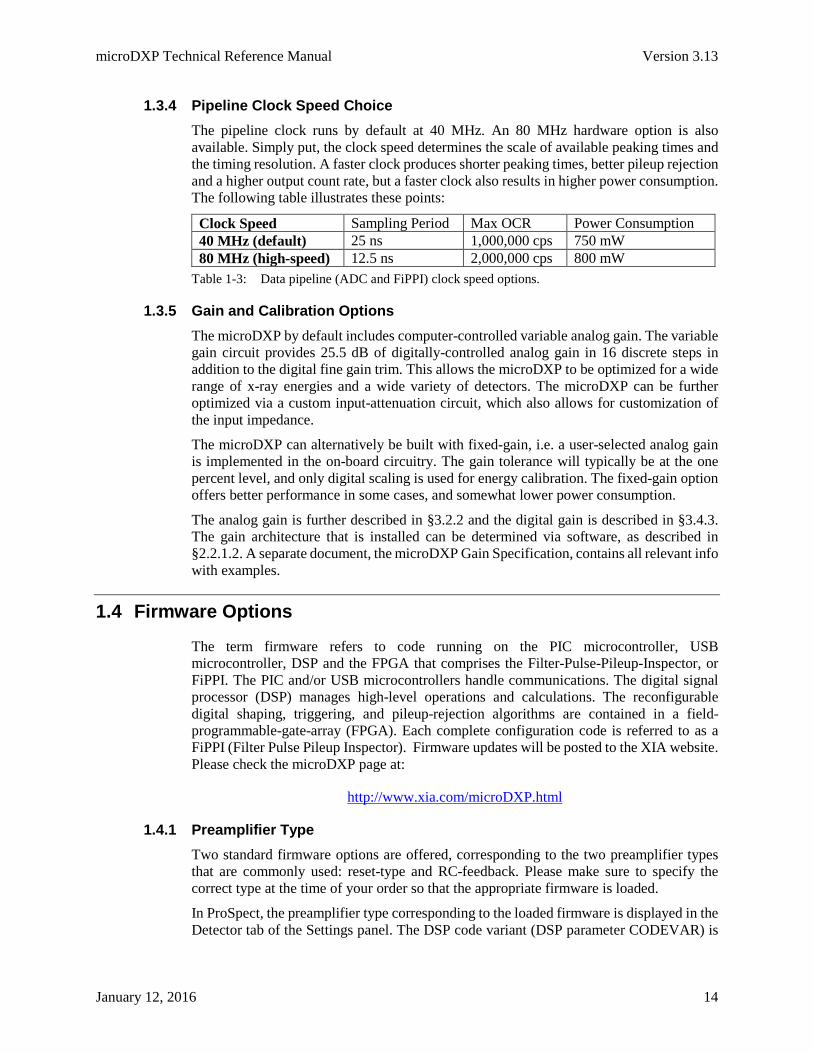
1.3.4 Pipeline Clock Speed Choice The pipeline clock runs by default at 40 MHz. An 80 MHz hardware option is also available. Simply put, the clock speed determines the scale of available peaking times and the timing resolution. A faster clock produces shorter peaking times, better pileup rejection and a higher output count rate, but a faster clock also results in higher power consumption. The following table illustrates these points:
Clock Speed Sampling Period Max OCR Power Consumption 40 MHz (default) 25 ns 1,000,000 cps 750 mW 80 MHz (high-speed) 12.5 ns 2,000,000 cps 800 mW
Table 1-3: Data pipeline (ADC and FiPPI) clock speed options.
1.3.5 Gain and Calibration Options The microDXP by default includes computer-controlled variable analog gain. The variable gain circuit provides 25.5 dB of digitally-controlled analog gain in 16 discrete steps in addition to the digital fine gain trim. This allows the microDXP to be optimized for a wide range of x-ray energies and a wide variety of detectors. The microDXP can be further optimized via a custom input-attenuation circuit, which also allows for customization of the input impedance.
The microDXP can alternatively be built with fixed-gain, i.e. a user-selected analog gain is implemented in the on-board circuitry. The gain tolerance will typically be at the one percent level, and only digital scaling is used for energy calibration. The fixed-gain option offers better performance in some cases, and somewhat lower power consumption.
The analog gain is further described in §3.2.2 and the digital gain is described in §3.4.3. The gain architecture that is installed can be determined via software, as described in §2.2.1.2. A separate document, the microDXP Gain Specification, contains all relevant info with examples.
1.4 Firmware Options
The term firmware refers to code running on the PIC microcontroller, USB microcontroller, DSP and the FPGA that comprises the Filter-Pulse-Pileup-Inspector, or FiPPI. The PIC and/or USB microcontrollers handle communications. The digital signal processor (DSP) manages high-level operations and calculations. The reconfigurable digital shaping, triggering, and pileup-rejection algorithms are contained in a field-programmable-gate-array (FPGA). Each complete configuration code is referred to as a FiPPI (Filter Pulse Pileup Inspector). Firmware updates will be posted to the XIA website. Please check the microDXP page at:
http://www.xia.com/microDXP.html
1.4.1 Preamplifier Type Two standard firmware options are offered, corresponding to the two preamplifier types that are commonly used: reset-type and RC-feedback. Please make sure to specify the correct type at the time of your order so that the appropriate firmware is loaded.
In ProSpect, the preamplifier type corresponding to the loaded firmware is displayed in the Detector tab of the Settings panel. The DSP code variant (DSP parameter CODEVAR) is
microDXP Technical Reference Manual Version 3.13
January 12, 2016 15
always even, e.g. “0”, for reset-type preamplifiers, and odd, e.g. “1”, for RC-feedback preamplifiers.
1.4.2 Custom Firmware Embedded systems customers often need special features or functionality that are not provided by the standard firmware set. Please contact XIA to discuss firmware customizations for your application:
1.5 Application Examples
The microDXP miniaturized circuit-board can easily be incorporated into a variety of benchtop, portable, networked and embedded x-ray and -ray spectroscopy data acquisition systems. The examples below illustrate the instrument’s flexibility.
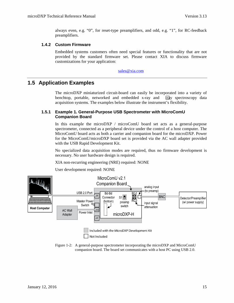
1.5.1 Example 1. General-Purpose USB Spectrometer with MicroComU Companion Board In this example the microDXP / microComU board set acts as a general-purpose spectrometer, connected as a peripheral device under the control of a host computer. The MicroComU board acts as both a carrier and companion board for the microDXP. Power for the MicroComU/microDXP board set is provided via the AC wall adapter provided with the USB Rapid Development Kit.
No specialized data acquisition modes are required, thus no firmware development is necessary. No user hardware design is required.
XIA non-recurring engineering (NRE) required: NONE
User development required: NONE
Figure 1-2: A general-purpose spectrometer incorporating the microDXP and MicroComU companion board. The board set communicates with a host PC using USB 2.0.

microDXP Technical Reference Manual Version 3.13
January 12, 2016 16
1.5.2 Example 2. General-Purpose Spectrometer Using RS232 and Custom Breakout Board In this example the microDXP acts as a general-purpose spectrometer, connected as a peripheral device under the control of the host computer. No specialized data acquisition modes are required, thus no firmware development is necessary. Some user hardware design is, however, required.
XIA non-recurring engineering (NRE) required: NONE.
User development required:
1. To connect to the external host, only a simple routing adapter interface unit is required to break out the microDXP high-density internal connection to standard RS-232 and power connections. At a minimum, this interface is a wire harness but could entail a printed circuit board with a small number of passive components.
2. Power supplies for the microDXP must be provided. Optional voltage regulators for the analog circuitry are included on the microDXP for systems in which high-quality power supplies are not available.
3. Some additional mechanical design, i.e. enclosure design, may be necessary.
The microDXP, power supplies and ‘routing-adapter’ together constitute a spectrometer that can be connected to virtually any controller with RS-232 communications. Note: The microCOMU interface board included with the Development Kit falls into this category.
MicroDXP board dimensions and mounting information, the connector locations and specifications, and the power supply specifications are all found in Appendix A of this manual.
Figure 1-3: A general-purpose spectrometer incorporating the microDXP. A simple user-designed routing-adapter interface connects the microDXP to the host computer and power supplies.
1.5.3 Example 3. Dedicated Spectrometer Using RS232 This example considers a materials sorting application where objects with certain pre-defined alloy ratios X, Y and Z are to be separated from others. An x-ray source irradiates incoming samples, and incident x-rays are collected by a solid-state detector connected to the microDXP. The microDXP is configured to assert a combination of its auxiliary digital I/O lines whenever the peak ratio X, Y or Z is detected. The digital I/O lines drive electromechanical or pneumatic components in real-time to execute the appropriate
microDXP Technical Reference Manual Version 3.13
January 12, 2016 17
mechanical operation, e.g. put the recognized object in the desired bin. User controls are limited to starting and stopping the system, and selecting one out of a small number of operating modes. Power supplies for the microDXP are also included. Finally, an external data port (e.g. RS-232) is also included so that ratios corresponding to new alloys can be defined, and new firmware uploaded without dismantling the hardware; or, alternatively, the microDXP could periodically be run in full MCA mode under computer control for diagnostic purposes.
This example demonstrates a system that uses a very small data acquisition command set (i.e. ‘start run’ and ‘stop run’) but that, conversely, requires customizations to the microDXP as well as significantly more user-designed hardware.
XIA non-recurring engineering (NRE) required:
1. Customized PIC microcontroller code is required to implement the I2C peripheral device control.
2. Customized PIC microcontroller code is required to implement high-level data acquisition routines controlled through the user pushbutton interface.
3. Customized DSP code is required for peak ratio calculations, possibly implemented in lookup tables.
4. Minimal FiPPI (FPGA) code modification is required to implement the auxiliary digital I/O functionality.
User development required:
1. A more advanced interface unit is required to break out the microDXP high-density internal connection to standard RS-232, auxiliary and power connections. Still, this interface does not involve many active components, i.e. the I2C and auxiliary digital I/O are simply routed to additional connectors. The pushbutton interface might include an additional microcontroller, but could be implemented simply in logic.
2. As drawn, the power supply is integrated on the interface board, with the same requirements as in the previous example. As stated there, optional voltage regulators for the analog circuitry are included on the microDXP for systems in which high-quality power supplies are not available.
3. Again, some additional mechanical design, i.e. enclosure design, may be necessary.
microDXP Technical Reference Manual Version 3.13
January 12, 2016 18
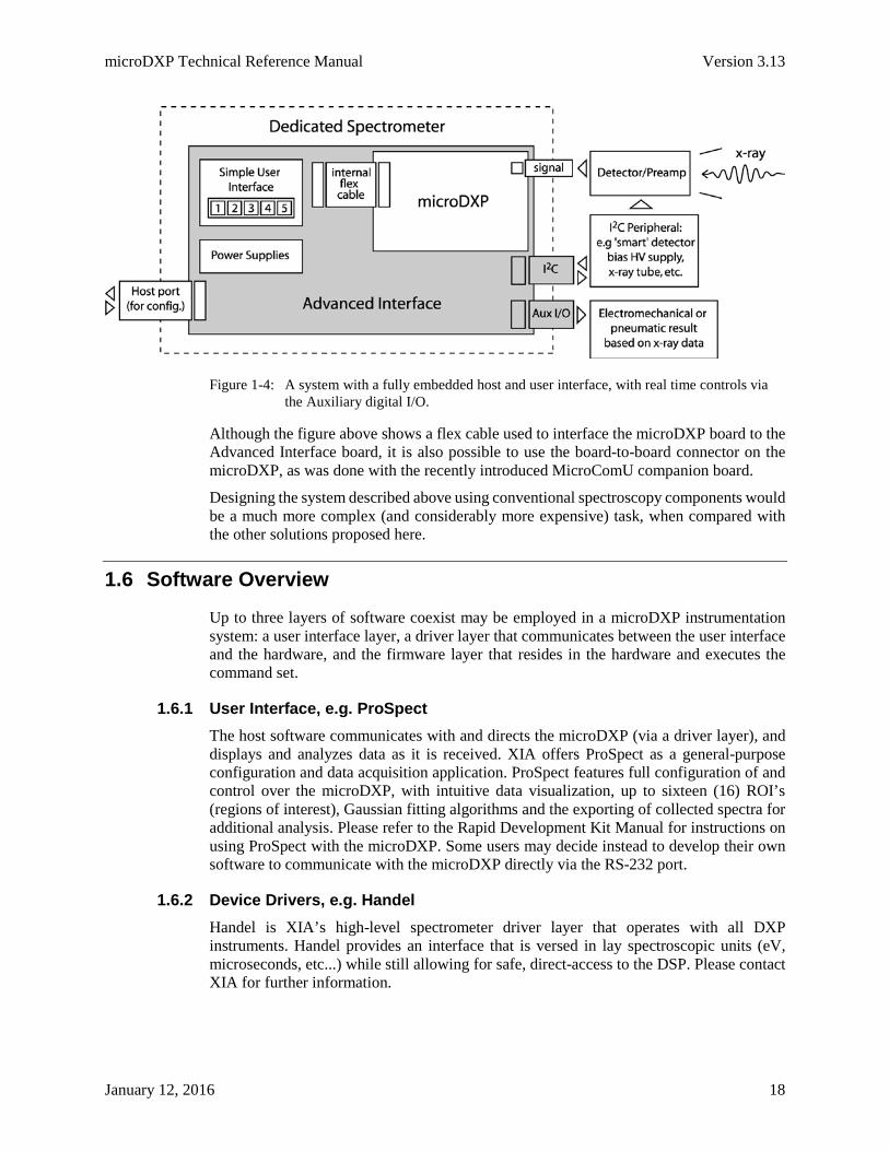
Figure 1-4: A system with a fully embedded host and user interface, with real time controls via the Auxiliary digital I/O.
Although the figure above shows a flex cable used to interface the microDXP board to the Advanced Interface board, it is also possible to use the board-to-board connector on the microDXP, as was done with the recently introduced MicroComU companion board.
Designing the system described above using conventional spectroscopy components would be a much more complex (and considerably more expensive) task, when compared with the other solutions proposed here.
1.6 Software Overview
Up to three layers of software coexist may be employed in a microDXP instrumentation system: a user interface layer, a driver layer that communicates between the user interface and the hardware, and the firmware layer that resides in the hardware and executes the command set.
1.6.1 User Interface, e.g. ProSpect The host software communicates with and directs the microDXP (via a driver layer), and displays and analyzes data as it is received. XIA offers ProSpect as a general-purpose configuration and data acquisition application. ProSpect features full configuration of and control over the microDXP, with intuitive data visualization, up to sixteen (16) ROI’s (regions of interest), Gaussian fitting algorithms and the exporting of collected spectra for additional analysis. Please refer to the Rapid Development Kit Manual for instructions on using ProSpect with the microDXP. Some users may decide instead to develop their own software to communicate with the microDXP directly via the RS-232 port.
1.6.2 Device Drivers, e.g. Handel Handel is XIA’s high-level spectrometer driver layer that operates with all DXP instruments. Handel provides an interface that is versed in lay spectroscopic units (eV, microseconds, etc...) while still allowing for safe, direct-access to the DSP. Please contact XIA for further information.
microDXP Technical Reference Manual Version 3.13
January 12, 2016 19
1.6.3 Firmware The microDXP operates with a relatively simple command set, accommodating easy implementation into embedded systems. Please refer to the RS-232 Command Specification (a separate document) for a detailed presentation of the complete command set. DXP-related documents are available online at:
http://www.xia.com/microDXP.html
1.7 Support
A unique benefit of dealing with a small company like XIA is that the same people who designed them often provide the technical support for our sophisticated instruments. Our customers are thus able to get an in-depth technical advice on how to fully utilize our products within the context of their particular applications. Please read through this brief chapter before contacting us.
XIA LLC
31057 Genstar Rd.
Hayward, CA 94544 USA
+1 (510) 401-5760
Email Support: [email protected]
1.7.1 Software and Firmware Updates It is important that the microDXP unit is being driven by the most recent software/firmware combination, since most problems are actually solved at the software level. Please check for the most up to date standard versions of the microDXP software and firmware at:
http://www.xia.com/microDXP.html
Please contact XIA if you are running semi-custom or proprietary firmware code. (Note: it is not a bad idea to make backup copies of your existing software and firmware before you update).
1.7.2 XUP Utility and Firmware Updates Firmware updates will be provided in the XUP format, which is only supported by ProSpect. ProSpect’s XUP utility also supports the import and export of parameter settings to and from non-volatile memory, such that multiple identical systems can easily be configured.
1.7.3 Related Documentation As a first step in diagnosing a problem, it is sometimes helpful to consult the most recent data sheets and user manuals for a given DXP product, available in the Adobe Portable Document Format (PDF) from the XIA web site. Since these documents may have been updated since the DXP unit was purchased, they may contain information that could help solving a problem in question. All manuals, datasheets, and application notes, as well as software and firmware downloads can be found on at:

microDXP Technical Reference Manual Version 3.13
January 12, 2016 20
http://www.xia.com/microDXP.html
In particular, we recommend that you download the following documents:
• microDXP Development Kit Manual – Quick start guide for the microDXP/microCOMU development kit hardware
• microDXP RS-232 Communications Specification – Detailed description of the RS-232 command set, for users who wish to develop their own software and/or hardware
• microDXP Gain Specification – Detailed description of the microDXP analog and digital gain, with examples
1.7.4 Email and Phone Support The microDXP comes with one year of email and phone support. Support can be renewed for a nominal fee. Please call XIA if your support agreement has expired.
The XIA Digital Processors (DGF & DXP) are digitally controlled, high performance products for X-ray and gamma-ray spectroscopy. All settings can be changed under computer control, including gains, peaking times, pileup inspection criteria, and ADC conversion gain. The hardware itself is very reliable. Most problems are not related to hardware failures, but rather to setup procedures and to parameter settings. XIA's DXP software includes several consistency checks to help select the best parameter values. However, due to large number of possible combinations the user may occasionally request parameter values which conflict among themselves. This can cause the DXP unit to report data that apparently make no sense (such as bad peak resolution or even empty spectra). Each time a problem is reported to us, we diagnose it and include necessary modifications in the new versions of our DXP control programs, as well as add the problem description to the FAQ list.
1.7.4.1 Submitting a problem report:
XIA encourages customers to report any problems encountered using any of our software. Unfortunately, due to limited resources XIA is unable to handle bug reports over the phone. In most cases, the XIA engineering team will need to review the bug information and run tests on their hardware before being able to respond.
All software-related bug reports should be emailed to [email protected] and should contain the following information, which will be used by our technical support personnel to diagnose and solve the problem:
• Your name and organization • Brief description of the application (type of detector, relevant experimental
conditions...etc.) • XIA hardware name and serial number • Version of the library (if applicable) • Operating System • Description of the problem; steps taken to re-create the bug • Supporting data:
The most important are DSP parameter settings, i.e. the gain, filter length, etc. The values of these parameters can be captured into an ASCII file in ProSpect. Please attach a copy of this file if possible. Capturing an oscilloscope image of the preamp output will be extremely helpful. This can done with the diagnostic tool included in ProSpect.

microDXP Technical Reference Manual Version 3.13
January 12, 2016 21
For general questions and DXP hardware issues please email [email protected]
1.7.5 Feedback XIA strives to keep up with the needs of our users. Please send us your feedback regarding the functionality and usability of the microDXP and ProSpect software. In particular, we are considering the following development issues:
1.7.5.1 Export File Formats
We would like to directly support as many spectrum file formats as possible. If we do not yet support it, please send your specification to [email protected]

microDXP Technical Reference Manual Version 3.13
January 12, 2016 22
2 Using the microDXP
This chapter provides a general outline of microDXP operations. XIA recommends using the ProSpect software as a microDXP configuration platform in all phases of production. For a step-by-step ‘Getting Started’ guide using ProSpect, including hardware setup instructions, please refer to the Rapid Development Kit User Manual. Though ProSpect also supports microDXP data acquisition (DAQ) procedures, many customers will necessarily use their own software when acquiring data. The most common procedures are explained below at the RS-232 command level. Please refer to Appendix E for a condensed summary of the RS-232 command and response protocol. Users who wish to develop the configuration routines into their software should refer to the RS-232 Command Specification (a separate document) for a detailed presentation of all RS-232 commands. DXP-related documents are available online at:
http://www.xia.com/microDXP.html
2.1 Hardware Settings
We recommend verifying the Preamplifier Type and Input Attenuation hardware settings before connecting the microDXP to a detector/preamplifier for the first time.
2.1.1 Preamplifier Type Selection The preamplifier type selector switch (if present) should already be set properly. Note that the setting must agree with the firmware that is loaded in non-volatile memory. The location of the miniature two-position slide switch S1 is displayed in Figure A-1 of Appendix A. The two positions are silkscreen-labeled RESET and RC. Select RESET for reset-type preamplifiers. Select RC for RC-feedback preamplifiers.
In ProSpect, the preamplifier type corresponding to the loaded firmware is displayed in the Detector tab of the Settings panel. The DSP code variant (DSP parameter CODEVAR) is always even, e.g. “0”, for reset-type preamplifiers, and odd, e.g. “1”, for RC-feedback preamplifiers.
2.1.2 Input Signal Attenuation The voltage range of the preamplifier signal must not exceed the input range of the microDXP, excluding reset transients that may exceed the range for a few microseconds. The input range and input impedance are specified below in Table 2-1.
Attenuation Setting Absolute Maximum Input Voltage Input Impedance Default – 0dB Attenuation (RG1 short, RG2 open)
+/- 4.0 V 10 KΩ
Option – 2.7dB Attenuation (RG1 open, RG2 short)
+/- 5.5 V 655 Ω
Custom Customer-defined Customer-defined Table 2-1: The attenuation setting determines the absolute maximum input voltage range and
input impedance
microDXP Technical Reference Manual Version 3.13
January 12, 2016 23
To accommodate preamplifiers with an output range in excess of +/-4 Volts, an optional attenuation setting is included. Attenuation and the increased input range are achieved by removing the solder from RG1 and shorting the two pads of RG2 together with solder. The microDXP input circuitry can be further customized to accommodate larger input voltage ranges or to change the input impedance. Contact XIA for assistance.
2.2 Board State and Configuration
The microDXP boots itself upon power up, and is shortly thereafter ready to acquire data with the same set of operating parameters used in the previous run. The first time the microDXP is powered on, detector and preamplifier related parameters will be in the factory default state. The settings should be optimized and saved to non-volatile on-board memory, such that they will automatically load during subsequent boot operations.
2.2.1 Board Information and Status General information about the hardware and firmware, and current board status can be retrieved.
In ProSpect, select Board Information… from the Tools menu to display the Board Information dialog. Select the Information tab to display information about the hardware and firmware configuration, variants and versions. Select the Status tab to display information about the current state of the PIC, DSP and data acquisition run.
The RS-232 command to read board information is 0x49. Please refer to the RS-232 Command Specification for details.
2.2.1.1 ADC Sampling Rate / DSP Clock Speed: DSPSPEED
It’s important to know the ADC sampling rate of your microDXP hardware. The default sampling rate is 40 MSPS, with a 25 ns sampling interval. A high-speed hardware variant operates at 80 MSPS, with a 12.5 ns sampling interval. See §3.3 for further details.
The ADC sampling rate is equivalent to the DSP Clock Speed (DSP parameter DSPSPEED), in MHz units, which is displayed in the Information tab of the Board Information dialog, or returned in response to the RS-232 command 0x49.
2.2.1.2 Gain Mode
The hardware gain variant, or Gain Mode, is encoded in the DSP parameter GAINMODE, which is included in the response to command 0x49: Get Board Information. In ProSpect, the Gain Mode is displayed in the Information tab of the Board Information dialog, accessible under the Tools menu. It can alternatively be determined from the value of GAINMODE in the DSP Parameters window, also accessible under the Tools menu.
Gain Mode GAINMODE Features Fixed + Digital 0 Analog Gain is fixed, equal to a customer-
defined Nominal Gain Digital Gain is used exclusively for MCA scaling and calibration
Switched + Digital 3 Analog gain is the product of Nominal Gain and Switched Gain, which is adjustable in 16 discrete increments

microDXP Technical Reference Manual Version 3.13
January 12, 2016 24
Digital Gain is used for MCA scaling and calibration
Table 2-2: Gain Modes supported by the new ‘blue’ microDXP
2.2.2 Serial Number In ProSpect, the serial number is automatically read at startup. It is displayed along the bottom of the main window, and in the Information tab of the Board Information dialog.
The RS-232 command to read the serial number is 0x48. Please refer to the RS-232 Command Specification for details.
2.2.3 On-Board Temperature The microDXP hardware includes an I2C thermometer. The temperature reading is not accessible in ProSpect.
The RS-232 command to read the on-board temperature is 0x41. Please refer to the RS-232 Command Specification for details.
2.3 Global Settings and the GLOBSET
The GLOBSET, specified in Appendix B, contains global settings including detector/preamplifier settings and system settings. There is only one GLOBSET—these settings are used for all peaking times and MCA formats.
The GLOBSET includes detector/preamplifier settings, advanced processor settings, run control settings and diagnostic control settings.
In ProSpect, GLOBSET settings are accessed via the Detector and Advanced tabs of the Settings panel. Because these settings are global, changes are simultaneously applied and saved to nonvolatile memory via the [Apply / Save] button.
2.3.1 Preamplifier Settings The microDXP’s analog hardware, firmware and a few settings must be configured to match the preamplifier.
2.3.1.1 Preamplifier Type
Please refer to §4.1 for more detailed description of charge-sensitive preamplifier topologies. Briefly, RC-feedback preamplifiers use resistive feedback to provide a continuous discharge path for the feedback capacitor, resulting in a characteristic decay time, e.g. 50 µs. Reset preamplifiers employ a switch to periodically discharge the capacitor very quickly, resulting in a periodic ‘staircase’ waveform with many x-ray steps between each reset, which rapidly returns the signal to its starting point.
The microDXP must have DSP and FPGA code pre-loaded in non-volatile memory that is appropriate for the preamplifier type used, and the microDXP hardware must be set type via a miniature DIP switch (refer to Appendix A for the switch location and settings).
In ProSpect, the preamplifier type corresponding to the loaded firmware is displayed in the Detector tab of the Settings panel. The DSP code variant (DSP parameter CODEVAR) is always even, e.g. “0”, for reset-type preamplifiers, and odd, e.g. “1”, for RC-feedback preamplifiers.

microDXP Technical Reference Manual Version 3.13
January 12, 2016 25
2.3.1.2 Decay Time: TAURC
If using an RC-feedback type preamplifier you must set the DSP parameter TAURC, which is expressed in units of the ADC sampling period. The decay time constant τRC in microseconds is:
τRC [µs] = TAURC / DSPSPEED Equation 2-1
In ProSpect, TAURC is set via the Decay Time field in the Detector tab of the Settings panel. Simply enter the desired value in microsecond units and press the [Apply / Save] button.
The RS-232 command to set and save TAURC to nonvolatile memory is 0x89. Please refer to the RS-232 Command Specification for details.
2.3.1.3 Reset Interval: RESETINT
If using a reset-type preamplifier you must set the DSP parameter RESETINT to the reset delay time or reset interval. This is the period after each preamplifier reset that the microDXP waits before re-enabling data acquisition. RESETINT, expressed in microseconds, is set based on the settling time of the preamplifier reset transient waveform, which typically ranges from hundreds of nanoseconds to hundreds of microseconds. Setting the delay shorter than the transient settling time typically degrades the energy resolution and may even introduce ‘reset artifact’ events, i.e. a false peak, into the spectrum. Setting the delay longer than necessary introduces additional processor dead time, which will reduce the data throughput at high count rates.
In ProSpect, RESETINT is set via the Reset Interval field in the Detector tab of the Settings panel. Simply enter the desired value in microsecond units and press the [Apply / Save] button.
The RS-232 command to set and save RESETINT to nonvolatile memory is 0x8A. Please refer to the RS-232 Command Specification for details.
2.3.1.4 Preamplifier Signal Polarity
Preamplifier signal polarity denotes the polarity of the preamplifier output signal. Please review §4.1 for a description and figures relating to the preamplifier signal polarity. Briefly, a positive polarity preamplifier produces a voltage step with a rising edge. The DSP parameter POLARITY must be set correctly.
In ProSpect, POLARITY is set via the Polarity field in the Detector tab of the Settings panel. Select the desired polarity and press the [Apply / Save] button.
The RS-232 command to set and save POLARITY to nonvolatile memory is 0x87. Please refer to the RS-232 Command Specification for details.
2.3.2 Advanced Processor Settings The advanced processor settings enable and disable various Digital X-ray Processor functions, and correspond to bits of the DSP parameter RUNTASKS. Typically these settings should only be modified as directed by XIA support staff.
In ProSpect, the advanced processor settings are accessed in the Advanced tab of the Settings panel.

microDXP Technical Reference Manual Version 3.13
January 12, 2016 26
2.4 MCA Settings and GENSETs
The GENSET, specified in Appendix C, is a table of MCA-related parameters, e.g. the number of bins and bin granularity, preset length of run, etc. Parameters within the GENSET can be modified and stored such that a standardized MCA format can be implemented with a single command. Five (5) GENSETs, and thus five MCA formats, can be stored and retrieved.
2.4.1 Selecting the GENSET In ProSpect, GENSET settings are accessed via the Acquisition tab of the Settings panel. GENSETs 0-4 can be selected via the GENSET drop-down list. Modifications to MCA settings can be tested by pressing the [Apply] button, and saved to nonvolatile memory via the [Save] button.
The RS-232 command to select a GENSET is 0x83. Note that this command simply retrieves one of five tables of MCA settings from nonvolatile memory. Please refer to the RS-232 Command Specification for details.
2.4.2 MCA Size and Bin Width The microDXP MCA format is quite flexible, with adjustable Number MCA Bins ranging up to 8192, and adjustable granularity via the MCA Bin Width setting. The DSP doesn’t constrain the relationship between these settings, so it’s possible to define a spectrum that exceeds the practical limits of the ADC, which should be avoided. As a rule-of-thumb, the product of Number MCA Bins and MCA Bin Width should not exceed 8192. If the product is larger than 8192 a dead region will be included at the high end of the spectrum, i.e. there is no possibility of getting counts in this region.
Number MCA Bins (MCALEN)
MCA Bin Width (BINMULTIPLE)
Product
8192 1 8192 4096 2 8192 2048 4 8192 1024 8 8192
Table 2-3: Maximum MCA Bin Width settings based upon the Number MCA Bins
The number of bins in the multi-channel analyzer (MCA) is determined by the DSP parameter MCALEN, ranging up to 8192 (8K). Note that changing MCALEN has no effect on the Digital Gain.
In ProSpect, MCALEN is set via the Number MCA Bins field in the Acquisition tab of the Settings panel. Select the desired number and press the [Apply] button to test the setting. Press the [Save] button to store the setting to the currently selected GLOBSET in nonvolatile memory.
The RS-232 command to set MCALEN is 0x85, and the command to save the current GENSET is 0x8F. Please refer to the RS-232 Command Specification for details.
The MCA Bin Width is determined by the DSP GENSET parameters BINGRANULAR and BINMULTIPLE, as shown in Equation 2-2. When the user sets BINGRANULAR ≤ 3, the DSP then sets BINMULTIPLE. Alternatively, the user can set BINGRANULAR = 4 (custom setting), and then set BINMULTIPLE directly to any integer.

microDXP Technical Reference Manual Version 3.13
January 12, 2016 27
MCA Bin Width = BINMULTIPLE = 2BINGRANULAR Equation 2-2
For simplicity, we recommend setting the BINGRANULAR = 4, such that the MCA Bin Width is set directly via BINMULTIPLE. Note that changing BINMULTIPLE (either directly or via BINGRANULAR) does affect the Digital Gain, per Equation 3-8.
In ProSpect, the MCA Bin Width is accessible in the Acquisition tab of the Settings panel. Select the desired setting and press the [Apply] button to test.
Note that the bin size (ev/Bin) changes as a result:
eV/Bin = Dynamic Range * MCA Bin Width
8000
Equation 2-3
As well as the energy range of the MCA spectrum:
Energy Range = Number MCA Bins * eV/Bin Equation 2-4
Press the [Save] button to store the setting to the currently selected GLOBSET in nonvolatile memory.
The RS-232 command to set BINGRANULAR and BINMULTIPLE is 0x84. As is done in ProSpect, we recommend always setting BINGRANULAR equal to 4, and setting the MCA Bin Width directly via BINMULTIPLE. Use command 0x8F to save the current GENSET. Please refer to the RS-232 Command Specification for details.
2.4.3 Base Gain, Switched Gain and Digital Base Gain Please first review §3.2.2 for a description of the updated analog gain circuitry and digital gain coefficient, and §2.2.1.2 to determine if the Switched Gain feature is installed.
The Base Gain, with range 1-100, refers to the product of the Switched-Gain and the Digital Base Gain. It should be set according to the dynamic range of the preamplifier signal, such that x-ray pulses and noise are properly digitized.
In ProSpect, we recommend first choosing a Dynamic Range, and then setting the Base Gain directly in the Acquisition tab of the Settings panel according to Equation 2-5. Alternatively, if the Preamplifier Gain is unknown, you can substitute a nominal value of 3 mV/keV and rely on the ROI calibration procedure to achieve the desired gain. Press the [Apply] button to test the new Base Gain. Press the [Save] button to store the setting to the currently selected GLOBSET in nonvolatile memory.
Base Gain = 1184
Dynamic Range [keV] * Preamplifier Gain [ mVkeV ]
Equation 2-5
After a preliminary value has been selected, the ROI calibration routine can be used to adjust the Base Gain, as described in the Development Kit Manual.
The RS-232 command to set the Switched Gain is 0x9B, and the command to change the Digital Base Gain is 0x9C. Briefly, choose the Switched Gain that best matches Equation

microDXP Technical Reference Manual Version 3.13
January 12, 2016 28
2-5 above, and then set the Digital Base Gain to compensate for the difference, as described in §3.4.3. Use command 0x8F to save the current GENSET. Please refer to the RS-232 Command Specification for details.
2.4.4 Reading the Current GENSET The RS-232 command to read the current GENSET table is 0x8E. Please refer to the RS-232 Command Specification for details.
2.4.5 Saving the Current GENSET to Non-Volatile Memory The RS-232 command to save the current GENSET table is 0x8F. Please refer to the RS-232 Command Specification for details.
2.5 Spectrometer Settings and PARSETs
The PARSET, specified in Appendix D, is a table of peaking-time-related spectrometer parameters, e.g. filter values, thresholds, pileup inspection settings, etc. Parameters within the PARSET can be modified and stored such that a calibrated spectrum with optimal settings is achieved whenever the Peaking Time is subsequently selected. The PARSETs are stored in the nonvolatile flash memory. Twenty-Four (24) peaking time values, and thus 24 PARSETs, are available.
The PARSET also contains 5 sets of gain tweaking and threshold settings, each corresponding to the 5 GENSETs or MCA formats. Storing thresholds and gain settings for every combination of peaking time and MCA format eliminates the need for calibrating a given combination more than once.
The factory-set default spectrometer settings should be adequate to acquire a recognizable spectrum. To achieve optimal performance the spectrometer settings must be adjusted, and stored to non-volatile memory such that the optimized settings will be accessible in the future. The slow filter Peaking Time should be chosen as a balance between energy resolution and throughput requirements (see §4.10).
2.5.1 Selecting a PARSET Each PARSET corresponds to a Peaking Time. In ProSpect, PARSET settings are accessed via the Acquisition tab of the Settings panel. PARSETs 0-23 can be selected via the Peaking Time drop-down list. Modifications to spectrometer settings for the selected PARSET can be tested by pressing the [Apply] button, and saved to nonvolatile memory via the [Save] button. Note that if you attempt to change the Peaking Time after changing any PARSET settings, ProSpect will ask whether you want to abandon the changes or save them.
The RS-232 command to select a PARSET is 0x82. Note that this command simply retrieves one of twenty-four tables of spectrometer settings from nonvolatile memory. If you have modified any settings associated with the current PARSET they will be lost when command 0x82 is executed. Use command 0x8D to save the current PARSET table first. Please refer to the RS-232 Command Specification for details.
2.5.2 Thresholds Proper triggering on input events depends on good threshold settings, particularly for the so-called Trigger (fast filter) and Baseline (intermediate filter) thresholds. The DSP

microDXP Technical Reference Manual Version 3.13
January 12, 2016 29
parameters THRESHOLD, BASETHRESH and SLOWTHRESH correspond to thresholds applied to the Trigger (fast), Baseline (intermediate), and Energy (slow) filters, respectively. Please refer to section for a thorough discussion of thresholds.
Each PARSET includes 5 different settings for THRESHOLD, BASETHRESH and SLOWTHRESH, corresponding to the 5 MCA formats, or GENSETs.
In ProSpect, the threshold values for the current PARSET and GENSET are accessed via the Acquisition tab of the Settings panel. Enter the desired threshold settings. Settings for the current PARSET can be tested by pressing the [Apply] button, and saved to nonvolatile memory via the [Save] button.
The RS-232 command to modify thresholds is 0x86, and the command to save the current PARSET table is 0x8D. Please refer to the RS-232 Command Specification for details.
2.5.3 Baseline Average Length A running average of baseline measurements is computed, which is then subtracted from sampled peak values to compute the energy of corresponding incident x-rays. The number of baseline samples averaged is referred to as the Baseline Average Length. In the DSP this is converted into the parameter BLFILTER according to the equation:
Baseline Average Length = 32768 / BLFILTER Equation 2-6
Please refer to §4.4.3 for a thorough discussion of baseline averaging.
In ProSpect, Baseline Average Length is accessed in the Acquisition tab of the Settings panel. Select the desired multiple-of-2 value from the drop-down list. Modifications for the selected PARSET can be tested by pressing the [Apply] button, and saved to nonvolatile memory via the [Save] button.
The RS-232 command to modify BLFILTER is 0x92, and the command to save the current PARSET table is 0x8D. Please refer to the RS-232 Command Specification for details.
2.5.4 Fine Gain Trim The Fine Gain Trim, or per-peaking-time calibration, is stored in the PARSET. In fact there is a Fine Gain Trim value stored for every PARSET/GENSET combination, allowing for a unique overall gain setting for each combination. This feature, which is described further in §3.4.3.3, can be ignored if the energy is already calibrated to the required accuracy, e.g. if you are still working with the same Peaking Time setting at which the Base Gain was last calibrated.
In ProSpect, the Fine Gain Trim for the current PARSET and GENSET is displayed and directly editable in the Acquisition tab of the Settings panel, but we recommend modifying it indirectly through the [Adjust Gain Trim] button in the ROI panel, i.e. by assigning an energy value to a peak in the MCA spectrum. Settings for the current PARSET can be tested by pressing the [Apply] button, and saved to nonvolatile memory via the [Save] button.
The RS-232 command to modify the gain trim is 0x91, and the command to save the current PARSET table is 0x8D. Please refer to Equation 3-10 and the RS-232 Command Specification for details.
microDXP Technical Reference Manual Version 3.13
January 12, 2016 30
2.5.5 Advanced Filter Settings Several other digital filter parameters are available for modification. Please refer to Chapter 4 for a thorough discussion of digital filtering with the DXP.
In ProSpect, the filter parameters are accessed via the Acquisition tab of the Settings panel. Press the [Edit Filter Parameters] button and modify settings in the associated dialog. Modifications for the selected PARSET can be tested by pressing the [OK] button, and saved to nonvolatile memory via the [Save] button.
The RS-232 command to modify filter parameters is 0x8B, and the command to save the current PARSET table is 0x8D. Please refer to the RS-232 Command Specification for details.
2.5.6 Reading the Current PARSET The RS-232 command to read the current PARSET table is 0x8C. Please refer to the RS-232 Command Specification for details.
2.5.7 Saving the Current PARSET to Non-Volatile Memory In ProSpect, all changes to the current PARSET can be saved to nonvolatile memory via the [Save] button.
The RS-232 command to save the current PARSET table is 0x8D. Please refer to the RS-232 Command Specification for details.
2.6 Repetitive Configuration of Identical Systems
In cases where many microDXP cards are to be configured identically (or nearly identical) it may be desirable to ‘carbon-copy’ user settings that have been optimized. This procedure is supported in ProSpect. Note that gain variations between modules make fine gain tuning necessary for each microDXP.
2.6.1 Create Master Parameter Set… In ProSpect select Create Master Parameter Set… from the Firmware menu to save all parameters to XUP file format. Select the desired filename and location and press [Save].
2.6.2 Download a Master Parameter Set… In ProSpect select Download… from the Firmware menu to write the parameters in the XUP file you created to a second microDXP. Browse to the desired XUP file and location and press [Download].
2.7 Data Acquisition
This section describes the most common data acquisition procedures. The most common commands (i.e. start/stop run, readout data) are described below. Please refer to the RS-232 Command Specification (a separate document) for a detailed presentation of all RS-232 commands. DXP-related documents are available online at:
http://www.xia.com/microDXP.html
microDXP Technical Reference Manual Version 3.13
January 12, 2016 31
In ProSpect select the MCA tab in the Main panel.
2.7.1 Starting a Run Data acquisition runs can be configured to automatically terminate the run after a preset time or number of input or output counts has elapsed, as described below in §2.6.5. By default (i.e. PRESET = 0) the run continues until a ‘stop run’ command is issued.
In ProSpect, simply press the [Start Run] button. Normally, spectrum data and statistics are cleared at the beginning of a data acquisition run. To preserve data and statistics from the previous run, check the Resume checkbox before pressing the [Start Run] button.
The RS-232 command to start a data acquisition run is 0x00. Please refer to the RS-232 Command Specification for details.
2.7.2 Stopping a Run By default (i.e. PRESET = 0) a run in progress continues until a ‘stop run’ command is issued. The microDXP can be configured to automatically terminate until a preset time or number of input or output counts has elapsed, as described below in §2.6.5. In such cases the ‘stop run’ command overrides the run preset.
In ProSpect, simply press the [Stop Run] button.
The RS-232 command to stop a data acquisition run is 0x01. Please refer to the RS-232 Command Specification for details.
2.7.3 Reading a Spectrum The ‘read spectrum’ command supports readout of any contiguous region of the MCA data, extending, of course to the entire spectrum. Each MCA bin is represented in DSP program memory as a 24-bit word (i.e. 3 bytes), supporting up to 16,777,215 counts per bin. In some cases (i.e. for short runs and/or low count rates) the upper bits of each bin word will always be zero. The readout speed can be increased by opting to read out a fewer number of bytes per bin, or DEPTH. At DEPTH=2 up to 65,535 counts per bin are supported. At DEPTH=1 up to 255 counts per bin are supported. Note: If the number of counts in a bin exceeds the DEPTH, the resulting distribution will display sharp discontinuities. The data is however always stored internally in the DSP at the full 24 bits. It is thus not necessary to restart the run when the DEPTH is exceeded: Simply change DEPTH and re-read the spectrum.
In ProSpect, the spectrum and statistics can be updated automatically or manually. Check the Continuous checkbox for automatic updates. If the checkbox is unchecked press the [Update] button to manually update the spectrum and statistics. Select Save MCA Data… from the File menu to save the data to file in ASCII format.
The RS-232 command to read the MCA spectrum is 0x02. Please refer to the RS-232 Command Specification for details.
2.7.4 Reading (and Calculating) the Run Statistics The ‘read run statistics’ command retrieves the Livetime (48-bit LIVETIME) of the triggering filter, the Realtime (48-bit REALTIME), the number of input counts (32-bit FASTPEAKS) and the number of output Events (32-bit EVENTSINRUN). These parameters can be used to directly calculate the input count rate (ICR), output count rate (OCR) and the Deadtime percentage:
microDXP Technical Reference Manual Version 3.13
January 12, 2016 32
ICR = FASTPEAKS / LIVETIME Equation 2-7
OCR = EVENTSINRUN / REALTIME Equation 2-8
Deadtime percentage = 1 - OCR / ICR Equation 2-9
REALTIME and LIVETIME are expressed in units of 500 ns. Note: Livetime corresponds to the triggering filter—NOT the energy filter—and thus does not alone determine the relationship between input and output count rates, i.e. the deadtime percentage.
In ProSpect, the spectrum and statistics can be updated automatically or manually. Check the Continuous checkbox for automatic updates. If the checkbox is unchecked press the [Update] button to manually update the spectrum and statistics.
The RS-232 command to read the run statistics is 0x06. Please refer to the RS-232 Command Specification for details.
2.7.5 Specifying fixed run lengths By default, the microDXP acquires data until a stop command is received from the host. Alternatively the microDXP can automatically terminate data acquisition runs based upon the real time, live time or the number of input or output counts exceeding a preset value. Note: Although the Realtime and Livetime are expressed in (measured accurately to) units of 500 nanoseconds, the process that monitors the real time and live time is only updated every 500 microseconds. Similarly, the input and output counts are tallied every 500 microseconds. The result is that a preset of 100,000 input counts may terminate with a slightly larger number of input events than 100,000. Nonetheless, the run statistics are all mutually consistent and accurate.
In ProSpect, select the desired Preset Run type from the drop-down list, and enter the desired value in the field below.
The RS-232 command to control preset run settings is 0x07. Please refer to the RS-232 Command Specification for details.
2.8 Diagnostic Tools
The microDXP provides for diagnostic readout of various signal vector, the baseline histogram, and all DSP parameters.
2.8.1 Diagnostic Trace The diagnostic trace, or Scope, feature acquires an 8000-point buffer of a user-selected source vector, at the user-selected sampling rate, according to user-selected trigger conditions for diagnostic readout.
In ProSpect, select the Scope tab in the Main panel. Select the Trace Type and enter the desired value in the Sampling Interval field. If desired select the Trigger Type (if any) and horizontal Position of the triggered event. Press the [Get Trace] button to refresh the display. Select Save Trace… from the File menu to save the data to file in ASCII format.
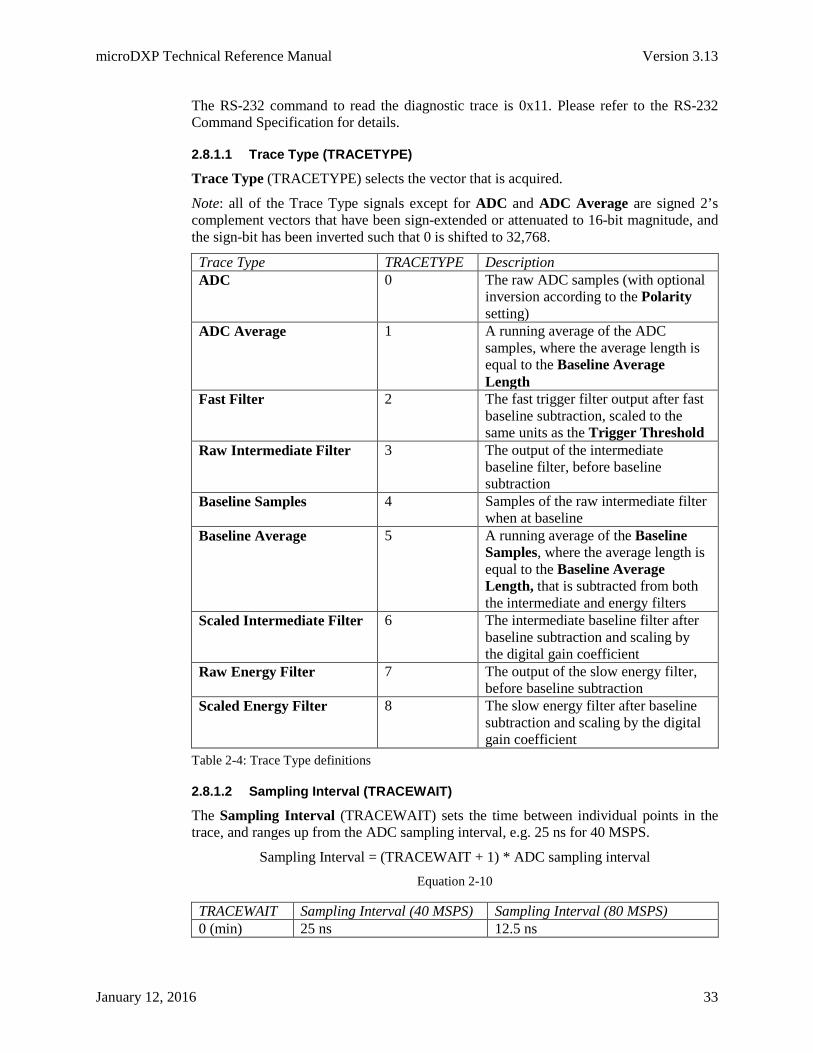
microDXP Technical Reference Manual Version 3.13
January 12, 2016 33
The RS-232 command to read the diagnostic trace is 0x11. Please refer to the RS-232 Command Specification for details.
2.8.1.1 Trace Type (TRACETYPE)
Trace Type (TRACETYPE) selects the vector that is acquired.
Note: all of the Trace Type signals except for ADC and ADC Average are signed 2’s complement vectors that have been sign-extended or attenuated to 16-bit magnitude, and the sign-bit has been inverted such that 0 is shifted to 32,768.
Trace Type TRACETYPE Description ADC 0 The raw ADC samples (with optional
inversion according to the Polarity setting)
ADC Average 1 A running average of the ADC samples, where the average length is equal to the Baseline Average Length
Fast Filter 2 The fast trigger filter output after fast baseline subtraction, scaled to the same units as the Trigger Threshold
Raw Intermediate Filter 3 The output of the intermediate baseline filter, before baseline subtraction
Baseline Samples 4 Samples of the raw intermediate filter when at baseline
Baseline Average 5 A running average of the Baseline Samples, where the average length is equal to the Baseline Average Length, that is subtracted from both the intermediate and energy filters
Scaled Intermediate Filter 6 The intermediate baseline filter after baseline subtraction and scaling by the digital gain coefficient
Raw Energy Filter 7 The output of the slow energy filter, before baseline subtraction
Scaled Energy Filter 8 The slow energy filter after baseline subtraction and scaling by the digital gain coefficient
Table 2-4: Trace Type definitions
2.8.1.2 Sampling Interval (TRACEWAIT)
The Sampling Interval (TRACEWAIT) sets the time between individual points in the trace, and ranges up from the ADC sampling interval, e.g. 25 ns for 40 MSPS.
Sampling Interval = (TRACEWAIT + 1) * ADC sampling interval Equation 2-10
TRACEWAIT Sampling Interval (40 MSPS) Sampling Interval (80 MSPS) 0 (min) 25 ns 12.5 ns
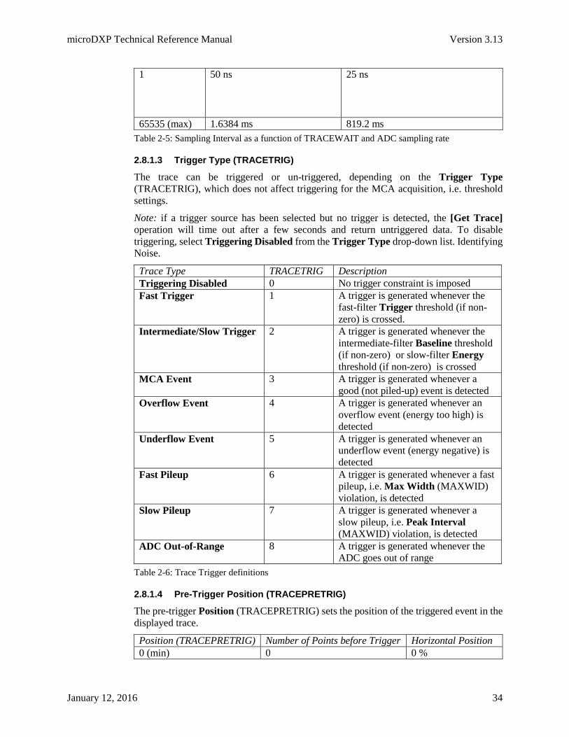
microDXP Technical Reference Manual Version 3.13
January 12, 2016 34
1 50 ns 25 ns
65535 (max) 1.6384 ms 819.2 ms Table 2-5: Sampling Interval as a function of TRACEWAIT and ADC sampling rate
2.8.1.3 Trigger Type (TRACETRIG)
The trace can be triggered or un-triggered, depending on the Trigger Type (TRACETRIG), which does not affect triggering for the MCA acquisition, i.e. threshold settings.
Note: if a trigger source has been selected but no trigger is detected, the [Get Trace] operation will time out after a few seconds and return untriggered data. To disable triggering, select Triggering Disabled from the Trigger Type drop-down list. Identifying Noise.
Trace Type TRACETRIG Description Triggering Disabled 0 No trigger constraint is imposed Fast Trigger 1 A trigger is generated whenever the
fast-filter Trigger threshold (if non-zero) is crossed.
Intermediate/Slow Trigger 2 A trigger is generated whenever the intermediate-filter Baseline threshold (if non-zero) or slow-filter Energy threshold (if non-zero) is crossed
MCA Event 3 A trigger is generated whenever a good (not piled-up) event is detected
Overflow Event 4 A trigger is generated whenever an overflow event (energy too high) is detected
Underflow Event 5 A trigger is generated whenever an underflow event (energy negative) is detected
Fast Pileup 6 A trigger is generated whenever a fast pileup, i.e. Max Width (MAXWID) violation, is detected
Slow Pileup 7 A trigger is generated whenever a slow pileup, i.e. Peak Interval (MAXWID) violation, is detected
ADC Out-of-Range 8 A trigger is generated whenever the ADC goes out of range
Table 2-6: Trace Trigger definitions
2.8.1.4 Pre-Trigger Position (TRACEPRETRIG)
The pre-trigger Position (TRACEPRETRIG) sets the position of the triggered event in the displayed trace.
Position (TRACEPRETRIG) Number of Points before Trigger Horizontal Position 0 (min) 0 0 %
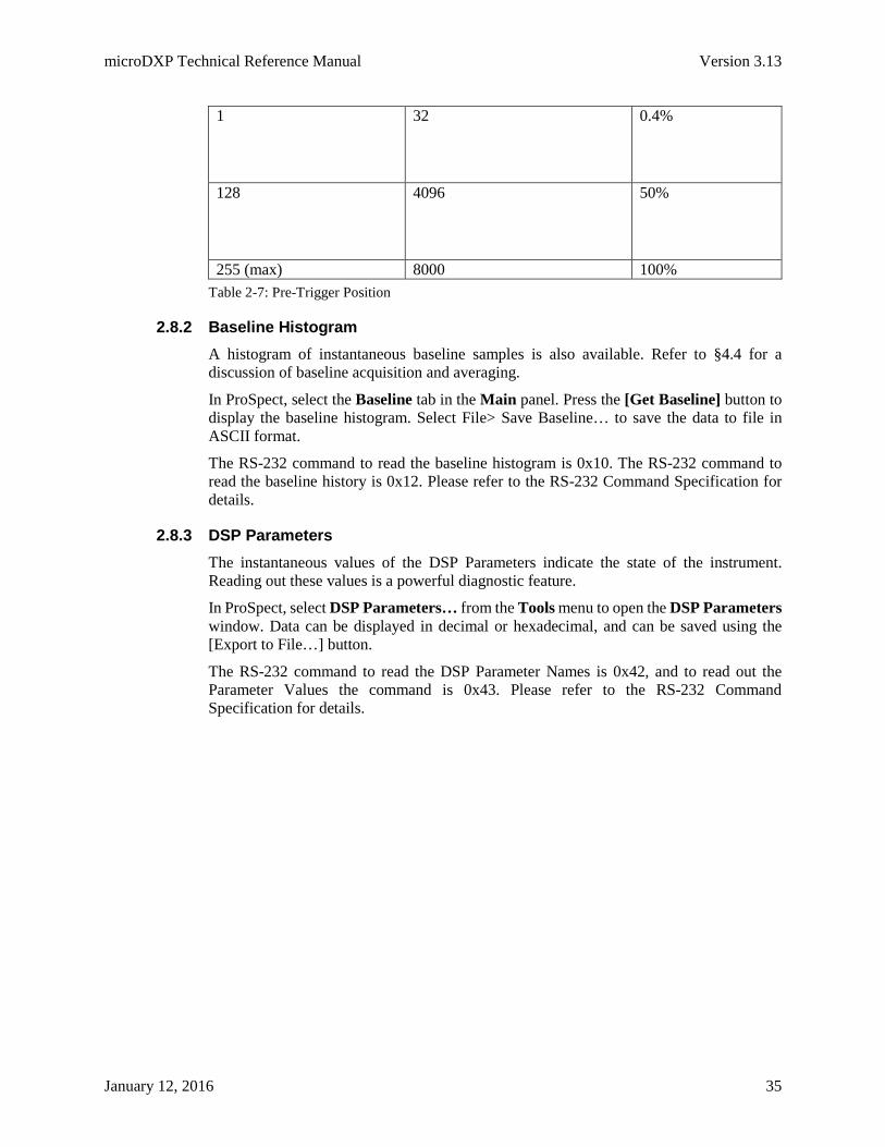
microDXP Technical Reference Manual Version 3.13
January 12, 2016 35
1 32 0.4%
128 4096 50%
255 (max) 8000 100% Table 2-7: Pre-Trigger Position
2.8.2 Baseline Histogram A histogram of instantaneous baseline samples is also available. Refer to §4.4 for a discussion of baseline acquisition and averaging.
In ProSpect, select the Baseline tab in the Main panel. Press the [Get Baseline] button to display the baseline histogram. Select File> Save Baseline… to save the data to file in ASCII format.
The RS-232 command to read the baseline histogram is 0x10. The RS-232 command to read the baseline history is 0x12. Please refer to the RS-232 Command Specification for details.
2.8.3 DSP Parameters The instantaneous values of the DSP Parameters indicate the state of the instrument. Reading out these values is a powerful diagnostic feature.
In ProSpect, select DSP Parameters… from the Tools menu to open the DSP Parameters window. Data can be displayed in decimal or hexadecimal, and can be saved using the [Export to File…] button.
The RS-232 command to read the DSP Parameter Names is 0x42, and to read out the Parameter Values the command is 0x43. Please refer to the RS-232 Command Specification for details.

microDXP Technical Reference Manual Version 3.13
January 12, 2016 36
3 MicroDXP Functional Description
3.1 Organizational Overview
The DXP channel architecture is shown in Figure 3-1. The four major operating blocks are the Analog Signal Conditioner (ASC), digital Filter, Peak detector, and Pileup Inspector (FiPPI), Digital Signal Processor (DSP), and PIC microcontroller. Also depicted are the ADC, the two host interface connections, a digital temperature sensor and the nonvolatile memory. The functions of each block are summarized below. This chapter does assume the reader has some familiarity with x-ray pulse processing theory and electronic devices. Please see Chapter 4 of this manual for a brief review.
Figure 3-1: Block diagram of the DXP channel architecture, showing the major functional sections and interface port options.
3.2 The Analog Signal Conditioner (ASC)
The ASC has three major functions: to reduce the dynamic range of the input signal and apply sufficient gain such that it can be adequately digitized by the 14-bit ADC, and to reduce the bandwidth of the resultant signal to meet the Nyquist criterion based upon the ADC sampling rate.

microDXP Technical Reference Manual Version 3.13
January 12, 2016 37
3.2.1 Dynamic Range Reduction In many cases, and particularly for reset-type preamplifiers, the full-scale output voltage range is much greater than the voltage step produced by a single x-ray event (see Figure 4-2). A high sampling rate is necessary to provide good pulse pileup detection, as described in §4.8, and sufficient ADC resolution is required to accurately sample the noise prior to the digital filters. For high count rates, pulse-pair resolution less than 50 ns is desirable, which implies a sampling rate of 40 MSPS or more. In order to reduce the noise σ in measuring Vx (see Figure 4-1 and Figure 4-3), experience shows that σ must be at least 4 times the ADC’s single bit resolution ∆V1. This effectively sets the gain of the amplifier stages preceding the ADC. Then, if the preamplifier’s full scale voltage range is Vmax, it must digitize to N effective bits, where N is given by:
N = log10 (Vmax/∆V1) / log10 (2) Equation 3-1
For a typical high-resolution spectrometer, N might be 16 or more. An ADC with 16 effective bits resolution that supports 40 MSPS is quite expensive (note that a typical 16-bit ADC has 13 or 14 effective bits). The alternative approach is to first reduce the dynamic range of the preamplifier output signal such that a moderately priced ADC can be used.
3.2.1.1 Reset-Type Preamplifiers
For reset-type preamplifiers the dynamic range reduction is accomplished using a novel technology, for which XIA has received US and international patents, and which is indicated in Figure 3-2. Here a preamplifier output is shown which cycles between roughly -3.0 Vand -0.25 V. We observe that it is not the overall function which is of interest, but rather the individual steps, such as shown in Figure 4-2 of the next chapter, that carry the x-ray amplitude information. Thus, if we know the average slope of the preamp output, we can generate a saw tooth function that has this average slope and restarts each time the preamplifier is reset, as shown in Figure 3-2. If we then subtract this saw tooth from the preamplifier signal, we can amplify the difference signal to match the ADC’s input range.
The generator required to produce this saw tooth function is quite simple, comprising a current integrator with an adjustable slope and a reset switch. A DAC (SLOPEDAC) controls the current, which sets the slope. The DAC input value is set algorithmically to maintain the ASC output (i.e. the “Amplified Sawtooth Subtracted Data” of Figure 3-2) within the ASC input range.
In practice, the large-signal dynamic range can be reduced by a factor of 8 to 16, thus reducing the required number of effective bits necessary to achieve the same resolution from 16 to a more easily achievable 12 or 13.

microDXP Technical Reference Manual Version 3.13
January 12, 2016 38
Figure 3-2: A saw tooth function having the same average slope as the preamp output, which ranges from -3.0 V to -0.25 V, is subtracted from it and the difference amplified and offset to match the 2.0 V input range of the ADC.
Occasionally, as also shown in Figure 3-2, fluctuations in data arrival rate will cause the conditioned signal to pass outside the ADC input range. This condition is detected by the FiPPI, which has digital discrimination levels set to ADC zero and full scale, which then remedies the situation by quickly closing the reset switch. During this so-called Tracking Step, data passed to the FiPPI are invalid. Preamplifier resets are detected similarly. Note: Data acquisition is halted until the time period defined by RESETINT has expired (see also §2.3.1.3).
3.2.1.2 RC-Feedback Preamplifiers
RC-feedback preamplifiers inherently produce a smaller dynamic range: At low rates the preamplifier output decays to baseline after each event, producing a voltage range on the order of a single event; at higher rates successive events add up, however, the larger the sum, the steeper the decay slope back to baseline. The result, as of course intended, is to yield a full-scale signal that increases only logarithmically with count rate.

microDXP Technical Reference Manual Version 3.13
January 12, 2016 39
Another consideration with RC-feedback preamplifiers is the DC offset. Although many such preamplifiers produce a ground-referenced output, many do not. Any offset is addressed in the microDXP by automatically adding a digitally controlled DC offset voltage to the input signal, such that the baseline value corresponds to 10% of the ADC input range.
3.2.2 Analog Gain The overall gain transfer function defines the relationship between the input x-ray pulse height and the resulting MCA bin, or measured energy. A separate document, the microDXP Gain Specification, describes the overall gain transfer function of the microDXP, and includes examples.
The original (green) microDXP used an off-the-shelf variable gain amplifier (VGA) to implement a continuously adjustable analog gain for both dynamic ranging and energy calibration. The single ‘base gain knob’ was easy to use, but we’ve found that VGA devices introduce excessive noise, temperature drift, and significant non-linearities into the signal.
In a significant departure from the previous design, the updated (blue) microDXP design now employs a digitally-controlled switched-gain amplifier architecture with 16 coarse analog gain settings for dynamic ranging in concert with finely adjustable digital gain for energy calibration. This approach adds some complexity to command and control because there are now two separate ‘base gain knobs’, but yields a superior pulse-height measurement. As before, a separate bin width setting defines the granularity, and thus the file size, of the MCA energy spectrum. A customer-defined fixed-gain hardware assembly option is available in volume production for applications where analog gain adjustment isn’t required.
Figure 3-3: The new microDXP gain architecture
The Analog Gain includes all gain elements in the front-end analog circuitry, i.e. it determines the pulse-height at the ADC for a preamplifier pulse-height ∆VPreamp:
∆VADC = Analog Gain * ∆VPreamp
Equation 3-2
The 14-bit ADC has an input range of 2.0V, thus the digitized pulse height in least-significant-bits is:

microDXP Technical Reference Manual Version 3.13
January 12, 2016 40
∆ADC = ∆VADC * 16384
2.0 V =
Analog Gain * ∆VPreamp * 163842.0 V
Equation 3-3
The Analog Gain is defined as the product of a fixed component called the Nominal Gain and the software-controlled component called the Switched Gain:
Analog Gain = Nominal Gain * Switched Gain Equation 3-4
The digitally-controlled Switched Gain circuit, with 16 discrete settings, allows the Analog Gain to be set according to the dynamic range of the input signal: it must be large enough such that electronic noise is sufficiently digitized, but small enough that the largest x-rays of interest fit well within the ADC input range. As a rule of thumb, the largest x-rays of interest should span no more than 50% of the ADC input range. Note that a customer-defined fixed-gain hardware assembly option, i.e. wherein the Nominal Gain is customer-defined and the Switched Gain circuit is omitted, is available in high-volume production for applications where the dynamic range of the input signal will not change.
3.2.2.1 Nominal Gain
The Nominal Gain is independent of software control. Its value is stored in non-volatile memory, accessible via the DSP parameters NOMGAIN (UQ1.15 format unsigned mantissa) and NOMGAINE (exponent). It is determined by the fixed amplification stages in the microDXP analog front-end circuit and by the Input Attenuation setting (see §2.1.2).
Nominal Gain = 0.825 * Input Attenuation Equation 3-5
Attenuation Setting Input Attenuation Nominal Gain 0 dB (default) 1.00 0.825 -2.5 dB (option) 0.75 0.619 Custom X 0.825 * X
Table 3-1: Relationship between Input Attenuation and Nominal Gain
3.2.2.2 Switched Gain
The Switched Gain is implemented with a new CMOS switched-feedback circuit with 16 discrete gain values controlled by the DSP parameter SWGAIN. The Switched Gain is linear-in-dB with SWGAIN, with approximately 1.7 dB increment, and units normalized to the Base Gain acquisition value in Handel. The discrete steps of the Switched Gain are smoothed when combined with the Digital Base Gain. Note that the Switched Gain circuit is omitted for the Fixed Gain hardware variant.
SWGAIN Switched Gain [dB] Switched Gain [V/V] Base Gain* 0 11.71 3.848 3.848 1 13.38 4.668 4.668 2 15.13 5.711 5.711 3 16.79 6.913 6.913 4 18.49 8.408 8.408 5 20.17 10.20 10.20 6 21.93 12.48 12.48
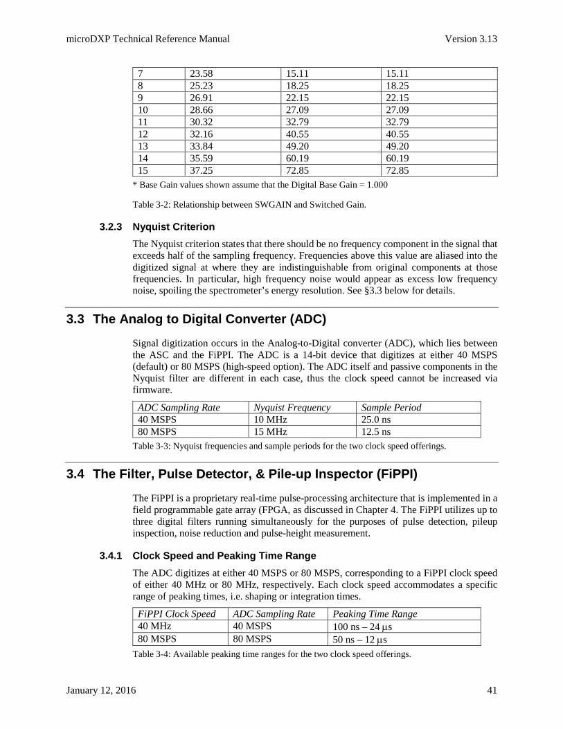
microDXP Technical Reference Manual Version 3.13
January 12, 2016 41
7 23.58 15.11 15.11 8 25.23 18.25 18.25 9 26.91 22.15 22.15 10 28.66 27.09 27.09 11 30.32 32.79 32.79 12 32.16 40.55 40.55 13 33.84 49.20 49.20 14 35.59 60.19 60.19 15 37.25 72.85 72.85
* Base Gain values shown assume that the Digital Base Gain = 1.000
Table 3-2: Relationship between SWGAIN and Switched Gain.
3.2.3 Nyquist Criterion The Nyquist criterion states that there should be no frequency component in the signal that exceeds half of the sampling frequency. Frequencies above this value are aliased into the digitized signal at where they are indistinguishable from original components at those frequencies. In particular, high frequency noise would appear as excess low frequency noise, spoiling the spectrometer’s energy resolution. See §3.3 below for details.
3.3 The Analog to Digital Converter (ADC)
Signal digitization occurs in the Analog-to-Digital converter (ADC), which lies between the ASC and the FiPPI. The ADC is a 14-bit device that digitizes at either 40 MSPS (default) or 80 MSPS (high-speed option). The ADC itself and passive components in the Nyquist filter are different in each case, thus the clock speed cannot be increased via firmware.
ADC Sampling Rate Nyquist Frequency Sample Period 40 MSPS 10 MHz 25.0 ns 80 MSPS 15 MHz 12.5 ns
Table 3-3: Nyquist frequencies and sample periods for the two clock speed offerings.
3.4 The Filter, Pulse Detector, & Pile-up Inspector (FiPPI)
The FiPPI is a proprietary real-time pulse-processing architecture that is implemented in a field programmable gate array (FPGA, as discussed in Chapter 4. The FiPPI utilizes up to three digital filters running simultaneously for the purposes of pulse detection, pileup inspection, noise reduction and pulse-height measurement.
3.4.1 Clock Speed and Peaking Time Range The ADC digitizes at either 40 MSPS or 80 MSPS, corresponding to a FiPPI clock speed of either 40 MHz or 80 MHz, respectively. Each clock speed accommodates a specific range of peaking times, i.e. shaping or integration times.
FiPPI Clock Speed ADC Sampling Rate Peaking Time Range 40 MHz 40 MSPS 100 ns – 24 µs 80 MSPS 80 MSPS 50 ns – 12 µs
Table 3-4: Available peaking time ranges for the two clock speed offerings.
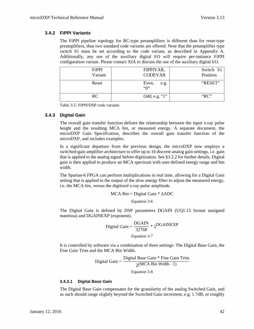
microDXP Technical Reference Manual Version 3.13
January 12, 2016 42
3.4.2 FiPPI Variants The FiPPI pipeline topology for RC-type preamplifiers is different than for reset-type preamplifiers, thus two standard code variants are offered. Note that the preamplifier type switch S1 must be set according to the code variant, as described in Appendix A. Additionally, any use of the auxiliary digital I/O will require per-instance FiPPI configuration variant. Please contact XIA to discuss the use of the auxiliary digital I/O.
FiPPI Variant
FIPPIVAR, CODEVAR
Switch S1 Position
Reset Even, e.g. “0”
“RESET”
RC Odd, e.g. “1” “RC”
Table 3-5: FiPPI/DSP code variants
3.4.3 Digital Gain The overall gain transfer function defines the relationship between the input x-ray pulse height and the resulting MCA bin, or measured energy. A separate document, the microDXP Gain Specification, describes the overall gain transfer function of the microDXP, and includes examples.
In a significant departure from the previous design, the microDXP now employs a switched-gain amplifier architecture to offer up to 16 discrete analog gain settings, i.e. gain that is applied to the analog signal before digitization. See §3.2.2 for further details. Digital gain is then applied to produce an MCA spectrum with user-defined energy range and bin width.
The Spartan-6 FPGA can perform multiplications in real time, allowing for a Digital Gain setting that is applied to the output of the slow energy filter to adjust the measured energy, i.e. the MCA bin, versus the digitized x-ray pulse amplitude.
MCA Bin = Digital Gain * ∆ADC Equation 3-6
The Digital Gain is defined by DSP parameters DGAIN (UQ1.15 format unsigned mantissa) and DGAINEXP (exponent).
Digital Gain = DGAIN32768
* 2DGAINEXP
Equation 3-7
It is controlled by software via a combination of three settings: The Digital Base Gain, the Fine Gain Trim and the MCA Bin Width.
Digital Gain = Digital Base Gain * Fine Gain Trim
2(MCA Bin Width - 1)
Equation 3-8
3.4.3.1 Digital Base Gain
The Digital Base Gain compensates for the granularity of the analog Switched Gain, and as such should range slightly beyond the Switched Gain increment, e.g. 1.7dB, or roughly
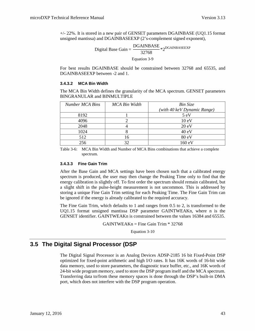
microDXP Technical Reference Manual Version 3.13
January 12, 2016 43
+/- 22%. It is stored in a new pair of GENSET parameters DGAINBASE (UQ1.15 format unsigned mantissa) and DGAINBASEEXP (2’s-complement signed exponent),
Digital Base Gain = DGAINBASE
32768*2DGAINBASEEXP
Equation 3-9
For best results DGAINBASE should be constrained between 32768 and 65535, and DGAINBASEEXP between -2 and 1.
3.4.3.2 MCA Bin Width
The MCA Bin Width defines the granularity of the MCA spectrum. GENSET parameters BINGRANULAR and BINMULTIPLE
Number MCA Bins MCA Bin Width Bin Size (with 40 keV Dynamic Range)
8192 1 5 eV 4096 2 10 eV 2048 4 20 eV 1024 8 40 eV 512 16 80 eV 256 32 160 eV
Table 3-6: MCA Bin Width and Number of MCA Bins combinations that achieve a complete spectrum.
3.4.3.3 Fine Gain Trim
After the Base Gain and MCA settings have been chosen such that a calibrated energy spectrum is produced, the user may then change the Peaking Time only to find that the energy calibration is slightly off. To first order the spectrum should remain calibrated, but a slight shift in the pulse-height measurement is not uncommon. This is addressed by storing a unique Fine Gain Trim setting for each Peaking Time. The Fine Gain Trim can be ignored if the energy is already calibrated to the required accuracy.
The Fine Gain Trim, which defaults to 1 and ranges from 0.5 to 2, is transformed to the UQ1.15 format unsigned mantissa DSP parameter GAINTWEAKn, where n is the GENSET identifier. GAINTWEAKn is constrained between the values 16384 and 65535.
GAINTWEAKn = Fine Gain Trim * 32768 Equation 3-10
3.5 The Digital Signal Processor (DSP
The Digital Signal Processor is an Analog Devices ADSP-2185 16 bit Fixed-Point DSP optimized for fixed-point arithmetic and high I/O rates. It has 16K words of 16-bit wide data memory, used to store parameters, the diagnostic trace buffer, etc., and 16K words of 24-bit wide program memory, used to store the DSP program itself and the MCA spectrum. Transferring data to/from these memory spaces is done through the DSP’s built-in DMA port, which does not interfere with the DSP program operation.
microDXP Technical Reference Manual Version 3.13
January 12, 2016 44
3.5.1 Parallel Flash EEPROM The microDXP also includes on-board non-volatile memory, which allows for the storage and retrieval of firmware and settings. A parallel flash EEPROM, accessed by the DSP, is used to store FiPPI configuration codes and parameter sets, i.e. the GLOBSET, GENSETS and PARSETS. The FiPPI is thus configured and optimized locally, with only a short command issued from the host. This stands in contrast to XIA’s benchtop instrument offerings, which typically require firmware to be downloaded from a host computer after power is turned on.
Parameter sets simplify data acquisition procedures. The DXP works well only if the internal parameters that govern digital filtering, peak detection and pileup inspection are properly set. For the lay user the optimization process can become overwhelming, particularly in an embedded systems environment. The microDXP approach is to optimize the relevant parameters for each peaking time once in the lab, and store the entire parameter set in a unique location in the flash memory. The exact state can be subsequently reproduced simply by selecting the saved parameter set. The flash memory can be updated with new FiPPI code via the RS-232, SPORT or IDMA ports.
3.5.2 Serial Port (SPORT) The Analog Devices DSP synchronous serial port, or SPORT, supports a variety of serial data communications protocols, and offers a maximum transfer rate of approximately 1Mbyte/sec. The SPORT interface is not supported by standard firmware, but may be a good candidate for custom multi-microDXP systems. The SPORT is included in both interface connectors (see §3.7 below).
3.5.3 DMA Port Parallel Direct Memory Access (DMA) provides the highest bandwidth communications path to the DSP data memory, and for this reason it is leveraged for both the on-board and off-board USB interface designs. Transfer rates up to 16 Mbytes/sec are possible. The DMA bus is directly available to the host via the high-speed board-to-board interface (see §3.7.2).
3.5.4 DSP Code Variants The same DSP code variant is now used for RC-type preamplifiers and reset-type preamplifiers: the DSP determines the preamplifier type according to the FiPPI variant, and prepares the FPGA registers accordingly. Special data acquisition modes (e.g. time-resolved spectroscopy, multi-SCA’s, etc.) do require variation in the DSP code. Please contact XIA to discuss your application.
3.6 PIC Microcontroller
The PIC microprocessor serves as the system controller, carrying out procedures to boot the board, loading appropriate DSP code from memory, and running acquisition routines. In addition the PIC handles I/O including RS-232 standard communications and an I2C bus for controlling dedicated peripheral devices.

microDXP Technical Reference Manual Version 3.13
January 12, 2016 45
3.6.1 RS-232 Serial Port The RS-232 serial port is the default communications interface for the microDXP, and is wired to both the flex-cable connector and the high-speed DMA port connector. Though relatively slow (115 kbaud typical, 921 kbaud maximum) the RS-232 port is in fact adequate for most applications. As one of the oldest communications standards, RS-232 enjoys wide compatibility with existing devices and is supported by all x86 Personal Computers.
3.6.2 I2C Serial Bus The I2C serial protocol allows for several serial devices to share the same two-wire bus through a device ID handshaking procedure. I2C devices are pre-programmed with a four-bit device ID (e.g. 1001 is used for some digital temperature sensors) appended with a 3-bit suffix that is typically set by hardwiring the appropriate pins to either the supply voltage or to ground. Two I2C devices are included on the microDXP itself (described below), and the bus is wired to both interface connectors to provide for microDXP control over, or monitoring of, other devices.
3.6.3 I2C EEPROM The I2C serial EEPROM, accessed by the PIC, is used to store the DSP code and general system information. The DSP is booted automatically upon power-up. The I2C memory can be updated with new DSP code via the RS-232 serial port.
3.6.4 I2C Temperature Sensor An I2C temperature sensor is included on the microDXP. The temperature measurement range is –55°C to +125°C, with ± 1°C accuracy.
3.6.5 PIC Code Variants Semi-custom and custom PIC code will be necessary for applications that utilize the I2C bus. Please contact XIA to discuss this development.
3.7 Interface to Host Computer
The microDXP interfaces to a host via one of three connectors: an on-board mini-USB connector, a flex-cable port or board-to-board connector. Please refer to Appendix A for connector locations and pinouts.
3.7.1 On-Board mini-USB 2.0 The microDXP now offers an on-board USB 2.0 interface, via a mini-USB connector. Power and auxiliary would still need to be provided separately, typically via the board-to-board connector.
3.7.2 Flex Cable Interface A 0.5mm-pitch flex-cable provides the connection to power, serial communications and auxiliary digital lines. The flex cable provides for two dimensions of freedom, but does require alignment along the axis that bisects all of the contacts.
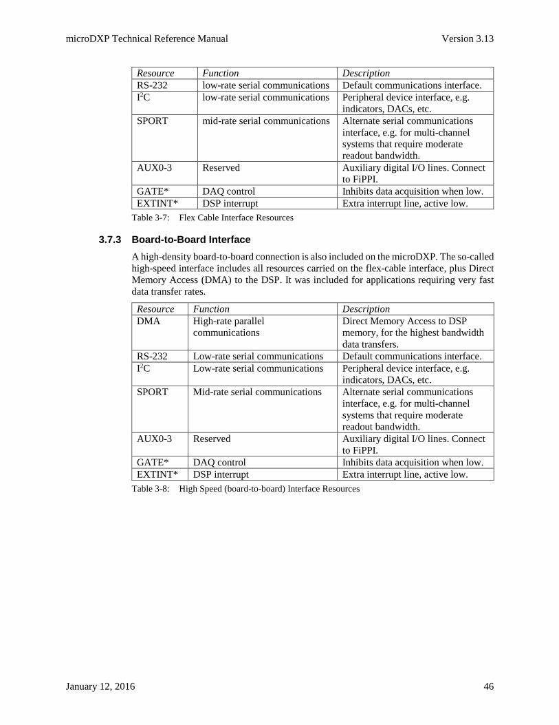
microDXP Technical Reference Manual Version 3.13
January 12, 2016 46
Resource Function Description RS-232 low-rate serial communications Default communications interface. I2C low-rate serial communications Peripheral device interface, e.g.
indicators, DACs, etc. SPORT mid-rate serial communications Alternate serial communications
interface, e.g. for multi-channel systems that require moderate readout bandwidth.
AUX0-3 Reserved Auxiliary digital I/O lines. Connect to FiPPI.
GATE* DAQ control Inhibits data acquisition when low. EXTINT* DSP interrupt Extra interrupt line, active low.
Table 3-7: Flex Cable Interface Resources
3.7.3 Board-to-Board Interface A high-density board-to-board connection is also included on the microDXP. The so-called high-speed interface includes all resources carried on the flex-cable interface, plus Direct Memory Access (DMA) to the DSP. It was included for applications requiring very fast data transfer rates.
Resource Function Description DMA High-rate parallel
communications Direct Memory Access to DSP memory, for the highest bandwidth data transfers.
RS-232 Low-rate serial communications Default communications interface. I2C Low-rate serial communications Peripheral device interface, e.g.
indicators, DACs, etc. SPORT Mid-rate serial communications Alternate serial communications
interface, e.g. for multi-channel systems that require moderate readout bandwidth.
AUX0-3 Reserved Auxiliary digital I/O lines. Connect to FiPPI.
GATE* DAQ control Inhibits data acquisition when low. EXTINT* DSP interrupt Extra interrupt line, active low.
Table 3-8: High Speed (board-to-board) Interface Resources
microDXP Technical Reference Manual Version 3.13
January 12, 2016 47
4 Digital Filtering: Theory of Operation and Implementation Methods
This chapter provides an in-depth discussion of x-ray pulse-processing theory both generally and as implemented in the microDXP. The topics include how digital filters work, x-ray detection, thresholds, baselines, pileup inspection, and input and output count rates. Topics are covered to illustrate the theoretical issues, practical implementation, and how to adjust parameters to obtain best performance.
The acronym DXP stands for “Digital X-ray Processor” and refers to XIA’s standard digital processing technology, which is included in many XIA products, including the microDXP.
4.1 X-ray Detection and Preamplifier Operation
Energy dispersive detectors, which include such solid state detectors as Si(Li), HPGe, HgI2, CdTe and CZT detectors, are generally operated with charge sensitive preamplifiers. When an x-ray is absorbed in the detector material it releases an electric charge Qx = Ex/ε, where the material constant ε is the amount of energy needed to form an electron-hole pair. Qy is integrated onto the preamplifier’s feedback capacitor Cf, to produce the voltage Vx = Qx/Cf = Ex/(εCf). Measuring the energy Ex of the x-ray therefore requires a measurement of the voltage step Vx in the presence of the amplifier’s noise σ. Figure 4-1 and Figure 4-3 depict reset-type and RC-type charge sensitive amplifiers, respectively. In both figures the detector D is biased by voltage source HV (either positive or negative) and connected to the input of amplifier A. Note that the signal polarity must be distinguished from the bias voltage polarity. The signal polarity is positive if the voltage step Vx is a rising edge, as displayed in Figure 4-1. Whether signal polarity is positive or negative depends upon the preamplifier’s design and does not depend upon bias voltage polarity, which is specified on the detector and is determined by its design.
4.1.1 Reset-Type Preamplifiers Figure 4-1a is a simplified schematic of a reset-type preamplifier, wherein Cf is discharged through the switch S from time to time when the amplifier’s output voltage gets so large that it behaves nonlinearly. Switch S may be an actual transistor switch, or may operate equivalently by another mechanism. In pulsed optical reset preamps light is directed at the amplifier A’s input FET to cause it to discharge Cf. In transistor reset preamps, the input FET may have an additional electrode which can be pulsed to discharge Cf. The output of a reset-type preamplifier following the absorption of an x-ray of energy Ex in detector D is a voltage step of amplitude Vx. Two x-ray steps are shown in Figure 4-1b as a step.

microDXP Technical Reference Manual Version 3.13
January 12, 2016 48
Figure 4-1: a) Reset-type charge sensitive preamplifier with a negatively biased detector; b) Output on absorption of x-ray rays. Note that the steps have a rising edge, so that the signal polarity is positive.
Figure 4-2 depicts the large-signal saw tooth waveform that results from successive x-ray steps followed by the reset. Note that the units here are Volts and milliseconds vs. millivolts and microseconds in the previous figure.
Figure 4-2: The large-signal reset waveform for a reset-type preamplifier with positive signal polarity, as displayed on a real oscilloscope. Note that the large signal character is not displayed in the microDXP diagnostic trace readout, e.g. used in ProSpect’s Scope diagnostic tool, looks quite different because of the dynamic range reduction carried out in the ASC, as described in §3.2.1.
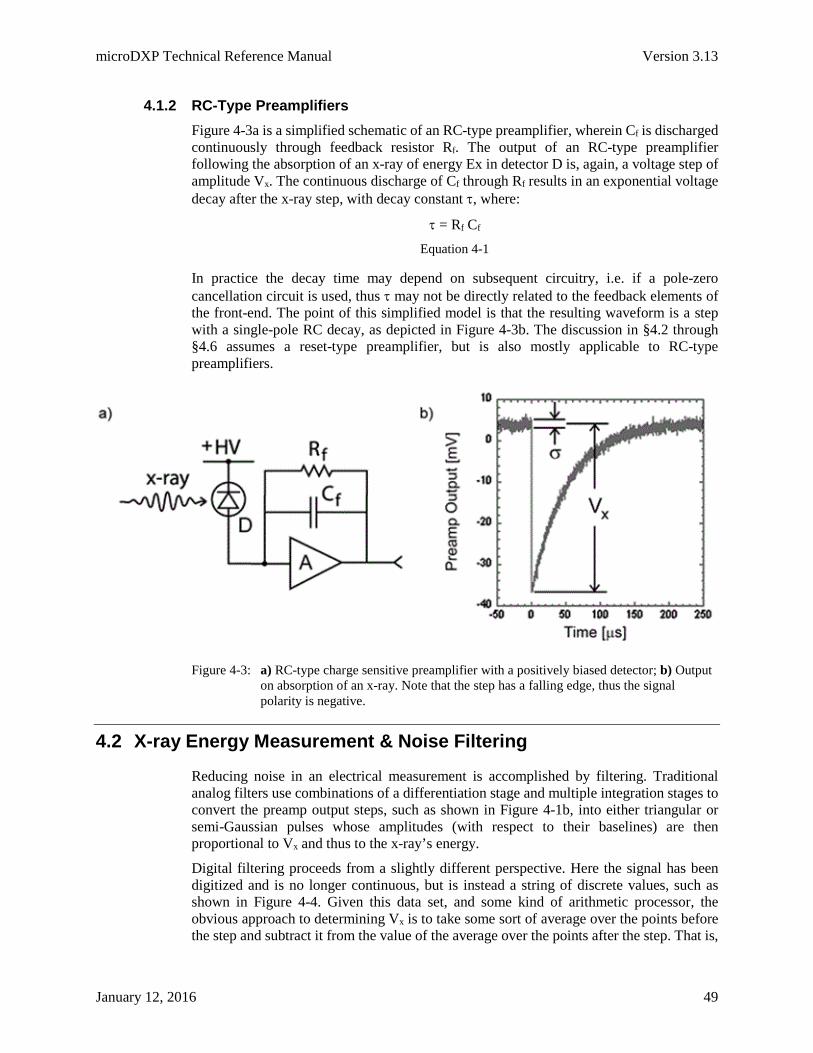
microDXP Technical Reference Manual Version 3.13
January 12, 2016 49
4.1.2 RC-Type Preamplifiers Figure 4-3a is a simplified schematic of an RC-type preamplifier, wherein Cf is discharged continuously through feedback resistor Rf. The output of an RC-type preamplifier following the absorption of an x-ray of energy Ex in detector D is, again, a voltage step of amplitude Vx. The continuous discharge of Cf through Rf results in an exponential voltage decay after the x-ray step, with decay constant τ, where:
τ = Rf Cf
Equation 4-1
In practice the decay time may depend on subsequent circuitry, i.e. if a pole-zero cancellation circuit is used, thus τ may not be directly related to the feedback elements of the front-end. The point of this simplified model is that the resulting waveform is a step with a single-pole RC decay, as depicted in Figure 4-3b. The discussion in §4.2 through §4.6 assumes a reset-type preamplifier, but is also mostly applicable to RC-type preamplifiers.
Figure 4-3: a) RC-type charge sensitive preamplifier with a positively biased detector; b) Output on absorption of an x-ray. Note that the step has a falling edge, thus the signal polarity is negative.
4.2 X-ray Energy Measurement & Noise Filtering
Reducing noise in an electrical measurement is accomplished by filtering. Traditional analog filters use combinations of a differentiation stage and multiple integration stages to convert the preamp output steps, such as shown in Figure 4-1b, into either triangular or semi-Gaussian pulses whose amplitudes (with respect to their baselines) are then proportional to Vx and thus to the x-ray’s energy.
Digital filtering proceeds from a slightly different perspective. Here the signal has been digitized and is no longer continuous, but is instead a string of discrete values, such as shown in Figure 4-4. Given this data set, and some kind of arithmetic processor, the obvious approach to determining Vx is to take some sort of average over the points before the step and subtract it from the value of the average over the points after the step. That is,
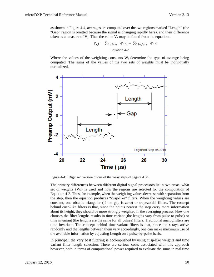
microDXP Technical Reference Manual Version 3.13
January 12, 2016 50
as shown in Figure 4-4, averages are computed over the two regions marked “Length” (the “Gap” region is omitted because the signal is changing rapidly here), and their difference taken as a measure of Vx. Thus the value Vx may be found from the equation:
𝑉𝑉𝑥𝑥,𝑘𝑘 = ∑ 𝑊𝑊𝑖𝑖𝑖𝑖(𝑎𝑎𝑎𝑎𝑎𝑎𝑎𝑎𝑎𝑎) 𝑉𝑉𝑖𝑖 − ∑ 𝑊𝑊𝑖𝑖𝑖𝑖(𝑏𝑏𝑎𝑎𝑎𝑎𝑏𝑏𝑎𝑎𝑎𝑎) 𝑉𝑉𝑖𝑖
Equation 4-2
Where the values of the weighting constants Wi determine the type of average being computed. The sums of the values of the two sets of weights must be individually normalized.
Figure 4-4: Digitized version of one of the x-ray steps of Figure 4.3b.
The primary differences between different digital signal processors lie in two areas: what set of weights Wi is used and how the regions are selected for the computation of Equation 4-2. Thus, for example, when the weighting values decrease with separation from the step, then the equation produces “cusp-like” filters. When the weighting values are constant, one obtains triangular (if the gap is zero) or trapezoidal filters. The concept behind cusp-like filters is that, since the points nearest the step carry more information about its height, they should be more strongly weighted in the averaging process. How one chooses the filter lengths results in time variant (the lengths vary from pulse to pulse) or time invariant (the lengths are the same for all pulses) filters. Traditional analog filters are time invariant. The concept behind time variant filters is that, since the x-rays arrive randomly and the lengths between them vary accordingly, one can make maximum use of the available information by adjusting Length on a pulse-by-pulse basis.
In principal, the very best filtering is accomplished by using cusp-like weights and time variant filter length selection. There are serious costs associated with this approach however, both in terms of computational power required to evaluate the sums in real time
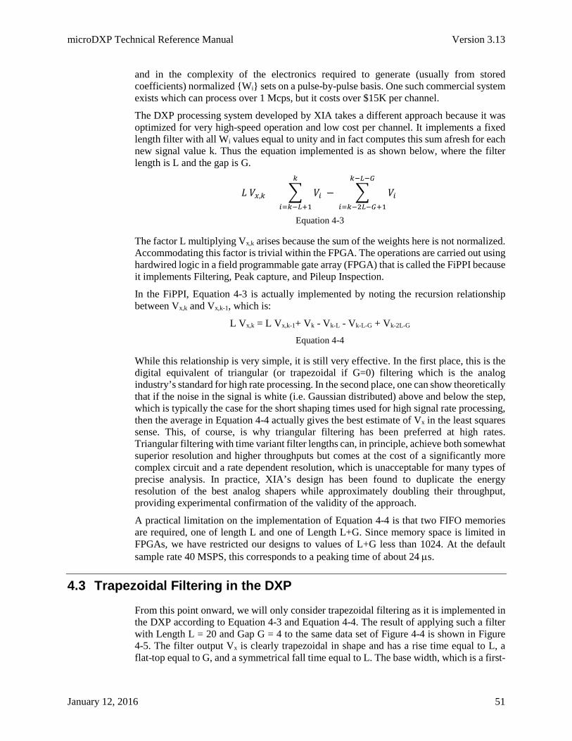
microDXP Technical Reference Manual Version 3.13
January 12, 2016 51
and in the complexity of the electronics required to generate (usually from stored coefficients) normalized Wi sets on a pulse-by-pulse basis. One such commercial system exists which can process over 1 Mcps, but it costs over $15K per channel.
The DXP processing system developed by XIA takes a different approach because it was optimized for very high-speed operation and low cost per channel. It implements a fixed length filter with all Wi values equal to unity and in fact computes this sum afresh for each new signal value k. Thus the equation implemented is as shown below, where the filter length is L and the gap is G.
𝐿𝐿 𝑉𝑉𝑥𝑥,𝑘𝑘 = 𝑉𝑉𝑖𝑖
𝑘𝑘
𝑖𝑖=𝑘𝑘−𝐿𝐿+1
− 𝑉𝑉𝑖𝑖
𝑘𝑘−𝐿𝐿−𝐺𝐺
𝑖𝑖=𝑘𝑘−2𝐿𝐿−𝐺𝐺+1
Equation 4-3
The factor L multiplying Vx,k arises because the sum of the weights here is not normalized. Accommodating this factor is trivial within the FPGA. The operations are carried out using hardwired logic in a field programmable gate array (FPGA) that is called the FiPPI because it implements Filtering, Peak capture, and Pileup Inspection.
In the FiPPI, Equation 4-3 is actually implemented by noting the recursion relationship between Vx,k and Vx,k-1, which is:
L Vx,k = L Vx,k-1+ Vk - Vk-L - Vk-L-G + Vk-2L-G Equation 4-4
While this relationship is very simple, it is still very effective. In the first place, this is the digital equivalent of triangular (or trapezoidal if G=0) filtering which is the analog industry’s standard for high rate processing. In the second place, one can show theoretically that if the noise in the signal is white (i.e. Gaussian distributed) above and below the step, which is typically the case for the short shaping times used for high signal rate processing, then the average in Equation 4-4 actually gives the best estimate of Vx in the least squares sense. This, of course, is why triangular filtering has been preferred at high rates. Triangular filtering with time variant filter lengths can, in principle, achieve both somewhat superior resolution and higher throughputs but comes at the cost of a significantly more complex circuit and a rate dependent resolution, which is unacceptable for many types of precise analysis. In practice, XIA’s design has been found to duplicate the energy resolution of the best analog shapers while approximately doubling their throughput, providing experimental confirmation of the validity of the approach.
A practical limitation on the implementation of Equation 4-4 is that two FIFO memories are required, one of length L and one of Length L+G. Since memory space is limited in FPGAs, we have restricted our designs to values of L+G less than 1024. At the default sample rate 40 MSPS, this corresponds to a peaking time of about 24 µs.
4.3 Trapezoidal Filtering in the DXP
From this point onward, we will only consider trapezoidal filtering as it is implemented in the DXP according to Equation 4-3 and Equation 4-4. The result of applying such a filter with Length L = 20 and Gap G = 4 to the same data set of Figure 4-4 is shown in Figure 4-5. The filter output Vx is clearly trapezoidal in shape and has a rise time equal to L, a flat-top equal to G, and a symmetrical fall time equal to L. The base width, which is a first-
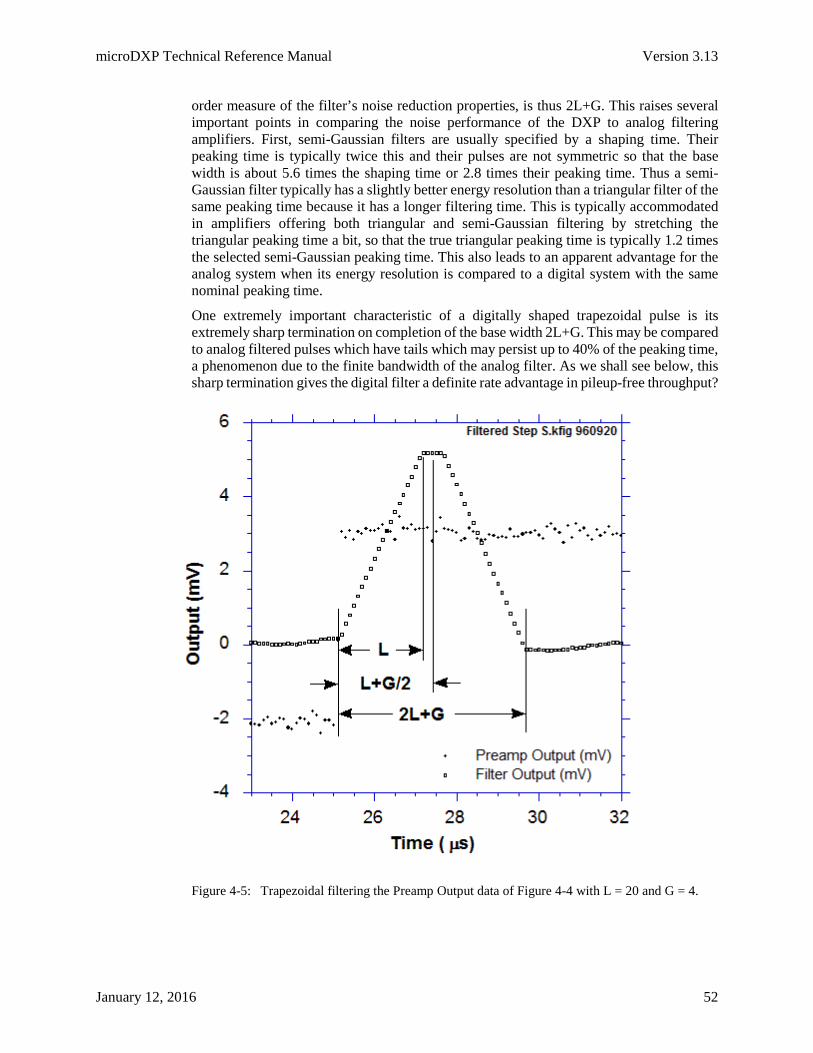
microDXP Technical Reference Manual Version 3.13
January 12, 2016 52
order measure of the filter’s noise reduction properties, is thus 2L+G. This raises several important points in comparing the noise performance of the DXP to analog filtering amplifiers. First, semi-Gaussian filters are usually specified by a shaping time. Their peaking time is typically twice this and their pulses are not symmetric so that the base width is about 5.6 times the shaping time or 2.8 times their peaking time. Thus a semi-Gaussian filter typically has a slightly better energy resolution than a triangular filter of the same peaking time because it has a longer filtering time. This is typically accommodated in amplifiers offering both triangular and semi-Gaussian filtering by stretching the triangular peaking time a bit, so that the true triangular peaking time is typically 1.2 times the selected semi-Gaussian peaking time. This also leads to an apparent advantage for the analog system when its energy resolution is compared to a digital system with the same nominal peaking time.
One extremely important characteristic of a digitally shaped trapezoidal pulse is its extremely sharp termination on completion of the base width 2L+G. This may be compared to analog filtered pulses which have tails which may persist up to 40% of the peaking time, a phenomenon due to the finite bandwidth of the analog filter. As we shall see below, this sharp termination gives the digital filter a definite rate advantage in pileup-free throughput?
Figure 4-5: Trapezoidal filtering the Preamp Output data of Figure 4-4 with L = 20 and G = 4.
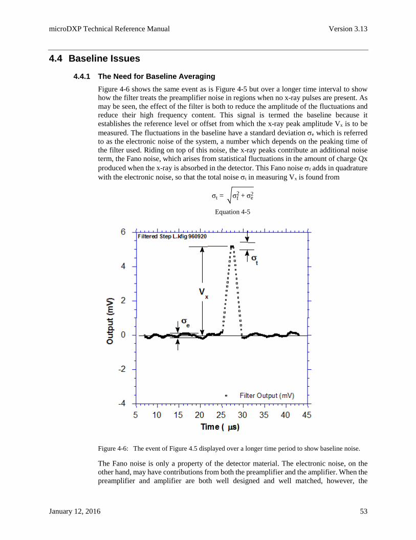
microDXP Technical Reference Manual Version 3.13
January 12, 2016 53
4.4 Baseline Issues
4.4.1 The Need for Baseline Averaging Figure 4-6 shows the same event as is Figure 4-5 but over a longer time interval to show how the filter treats the preamplifier noise in regions when no x-ray pulses are present. As may be seen, the effect of the filter is both to reduce the amplitude of the fluctuations and reduce their high frequency content. This signal is termed the baseline because it establishes the reference level or offset from which the x-ray peak amplitude Vx is to be measured. The fluctuations in the baseline have a standard deviation σe which is referred to as the electronic noise of the system, a number which depends on the peaking time of the filter used. Riding on top of this noise, the x-ray peaks contribute an additional noise term, the Fano noise, which arises from statistical fluctuations in the amount of charge Qx produced when the x-ray is absorbed in the detector. This Fano noise σf adds in quadrature with the electronic noise, so that the total noise σt in measuring Vx is found from
σt = σf2 + σe
2
Equation 4-5
Figure 4-6: The event of Figure 4.5 displayed over a longer time period to show baseline noise.
The Fano noise is only a property of the detector material. The electronic noise, on the other hand, may have contributions from both the preamplifier and the amplifier. When the preamplifier and amplifier are both well designed and well matched, however, the

microDXP Technical Reference Manual Version 3.13
January 12, 2016 54
amplifier’s noise contribution should be essentially negligible, though achieving this in the mixed analog-digital environment of a digital pulse processor is a non-trivial task.
In the general case, the mean baseline value is not zero. This situation arises whenever the slope of the preamplifier signal is not zero between x-ray pulses. This can be seen from Equation 4-3. When the slope is not zero, the mean values of the two sums will differ because they are taken over regions separated in time by L+G, on average. Such non-zero slopes can arise from various causes, of which the most common is detector leakage current.
When the mean baseline value is not zero, it must be determined and subtracted from measured peak values in order to determine Vx values accurately. If the error introduced by this subtraction is not to significantly increase σt, then the error in the baseline estimate σb must be small compared to σe. Because the error in a single baseline measurement is σe, by definition, this means that multiple baseline measurements will have to be averaged. This number, NB is the Baseline Average. For example, if NB = 128 measurements are averaged then the total noise will be as shown in Equation 4 6.
σt = σf2 + 1 +
1128
σe2
Equation 4-6
This results in less than 0.5 eV degradation in resolution when resolutions of order 130 eV are obtained.
4.4.2 Raw Baseline Measurement The output of the baseline filter (either the energy filter itself, or a derivative of it) is sampled periodically in the explicit absence of an x-ray step, defined by a baseline threshold. In practice, the DXP initially makes a series of NB baseline measurements to compute a starting baseline mean. It then makes additional baseline measurements at quasi-periodic intervals to keep the estimate up to date. These values are stored internally and can be read out to construct a spectrum of baseline noise, referred to as the Baseline Histogram. This is recommended because of its excellent diagnostic properties. When all components in the spectrometer system are working properly, the baseline spectrum should be Gaussian in shape with a standard deviation reflecting n. Deviations indicate various pathological conditions which may also cause the x-ray spectrum to be distorted and therefore have to be fixed.
The situation is remedied by removing (“cutting”) outlying samples from the baseline average described below. If the maximum in the baseline distribution lies at E0, then captured baseline values that deviate from E0 by more than ∆E are not included in the running baseline average. Note that all captured baseline values are included in the Baseline Histogram, however, so that it is always a valid representation of the system’s behavior.
4.4.3 Baseline Averaging in the DXP A running average of baseline measurements is computed, which is then subtracted from sampled peak values to compute the energy of corresponding incident x-rays. The number of baseline samples averaged is set in ProSpect as Baseline Average Length. In the DSP this is converted into the parameter BLFILTER according to the equation:

microDXP Technical Reference Manual Version 3.13
January 12, 2016 55
Baseline Average Length = 32768
BLFILTER
Equation 4-7
Physically, the baseline is a measure of the instantaneous slope (Volts/second) for a pulsed-reset detector, and a measure of the DC offset for an RC-feedback preamplifier. For a perfect detector and preamplifier the baseline value is independent of time. In fact, the variation in leakage current of the detector and offset drift and 1/f noise of the preamplifier contribute to a baseline value that wanders at low frequencies. The goal is to achieve a baseline average that has a sufficient number of samples to average out the high frequency noise, but which still reflects the ‘local’ instantaneous baseline. Generally speaking, Baseline Average Length is set to achieve the best energy resolution performance over the desired range of input count rate. There are two considerations worth emphasizing:
1. Excess detector/preamplifier noise and pickup: A high-frequency noise peak can result in poor relative performance at the corresponding ‘resonant’ peaking time. Often this problem can be mediated, though not eliminated, by increasing the number of baseline samples in the average for the affected peaking times. On the other hand, excess low-frequency noise, i.e. wandering, can be remedied by reducing the number baseline samples in the average.
2. High rate performance: At higher rates, i.e. > 50% deadtime, the slow filter returns less and less often to baseline, thus the time between baseline samples grows longer. This is the primary cause of degraded energy resolution at high rates. The microDXP now employs a proprietary circuit that virtually eliminates this problem, resulting in industry-leading count rate stability.
4.5 X-ray Detection & Setting Thresholds
Before capturing a value of Vx we must first detect the x-ray. X-ray steps (in the preamp output) are detected by digitally comparing the output of a trapezoidal filter to a threshold.
In the DXP up to three trapezoidal filters are implemented: fast, intermediate and slow; each with a threshold that can be individually enabled or disabled. A fast (trigger) filter very quickly detects larger x-ray steps. A slow (energy) filter averages out the most noise and can thus detect smaller x-ray steps, but has a response that is much slower. An intermediate (baseline) filter provides a balance between the speed of the fast filter and the noise reduction of the slow filter.
The fast filter is used solely for x-ray detection, i.e. a threshold crossing initiates event processing. Its short base width (2L+G) means that successive pulses that would ‘pile-up’ in slower filters can be resolved in the fast filter and rejected from the spectrum (see Figure 4-9 below). Conversely, little noise reduction is achieved in the fast filter, thus the fast threshold cannot be set to detect particularly low x-ray energies.
The intermediate filter threshold is applied as part of the baseline acquisition circuitry, i.e. baseline measurements are taken when the signal is below this threshold. Intermediate threshold crossings by default also trigger event processing, extending the detectable energy range significantly below the fast filter threshold. Note that this threshold is initialized to the maximum, i.e. most conservative, value, and should be adjusted downward by the user for best performance.
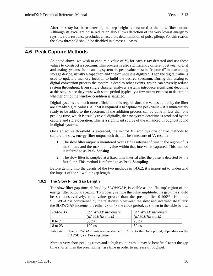
microDXP Technical Reference Manual Version 3.13
January 12, 2016 56
After an x-ray has been detected, the step height is measured at the slow filter output. Although its excellent noise reduction also allows detection of the very lowest energy x-rays, its slow response precludes an accurate determination of pulse pileup. For this reason the slow threshold should be disabled in almost all cases.
4.6 Peak Capture Methods
As noted above, we wish to capture a value of Vx for each x-ray detected and use these values to construct a spectrum. This process is also significantly different between digital and analog systems. In the analog system the peak value must be “captured” into an analog storage device, usually a capacitor, and “held” until it is digitized. Then the digital value is used to update a memory location to build the desired spectrum. During this analog to digital conversion process the system is dead to other events, which can severely reduce system throughput. Even single channel analyzer systems introduce significant deadtime at this stage since they must wait some period (typically a few microseconds) to determine whether or not the window condition is satisfied.
Digital systems are much more efficient in this regard, since the values output by the filter are already digital values. All that is required is to capture the peak value – it is immediately ready to be added to the spectrum. If the addition process can be done in less than one peaking time, which is usually trivial digitally, then no system deadtime is produced by the capture and store operation. This is a significant source of the enhanced throughput found in digital systems.
Once an active threshold is exceeded, the microDXP employs one of two methods to capture the slow energy filter output such that the best measure of Vx results:
1. The slow filter output is monitored over a finite interval of time in the region of its maximum, and the maximum value within that interval is captured. This method is referred to as Peak Sensing.
2. The slow filter is sampled at a fixed time interval after the pulse is detected by the fast filter. This method is referred to as Peak Sampling.
Before getting into the details of the two methods in §4.6.2, it’s important to understand the impact of the slow filter gap length.
4.6.1 The Slow Filter Gap Length The slow filter gap time, defined by SLOWGAP, is visible as the ‘flat-top’ region of the energy filter output trapezoid. To properly sample the pulse amplitude, the gap time should be set conservatively, to a value greater than the preamplifier 0-100% rise time. SLOWGAP is constrained by the relationship between the slow and intermediate filters: the SLOWGAP increment is either 2x or 4x the clock period, as shown in the table below.
PARSETs SLOWGAP increment (w/ 40MHz clock)
SLOWGAP increment (w/ 80MHz clock)
0 to 7 50 ns 25 ns 8 to 23 100 ns 50 ns
Table 4-1: The SLOWGAP units are constrained to 2x or 4x the clock period, depending on the PARSET, i.e. Peaking Time.
Note: at very short peaking times and at high count rates, it may be beneficial to set the gap time shorter than the preamplifier rise time in order to increase throughput.

microDXP Technical Reference Manual Version 3.13
January 12, 2016 57
4.6.2 Peak Sampling vs. Peak Sensing The figures below demonstrate the two approaches. In Peak Sensing mode the slow filter output is monitored over a finite interval of time, and the maximum value within that interval is selected. The interval is set automatically, solely based on the values of the DXP parameters SLOWLEN and PEAKINT. SLOWLEN and PEAKINT are both automatically derived from the peaking time value selected in ProSpect and should normally not be adjusted by the user. PEAKINT is also a pileup inspection parameter, as will be discussed in further detail in §4.8.
Figure 4-7: In the default Peak Sensing mode the slow filter output is monitored and the peak value is selected. This ‘automatic’ mode typically yields the best performance.
In Peak Sampling mode the slow filter output is instead sampled a fixed time after the x-ray is detected. An additional timer is started when an x-ray step is detected which expires after PEAKSAM clock cycles. PEAKSAM must be less than PEAKINT, and should typically be set such that the sample point lies in the ‘flat-top’ region of the slow filter output:
SLOWLEN ≤ PEAKSAM ≤ (SLOWLEN + SLOWGAP) Equation 4-8
The precise setting has a strong effect on energy resolution and should be determined empirically for each new detector. In most cases Peak Sensing mode will yield the best performance, and it is easier to use because there is one less setting to optimize.
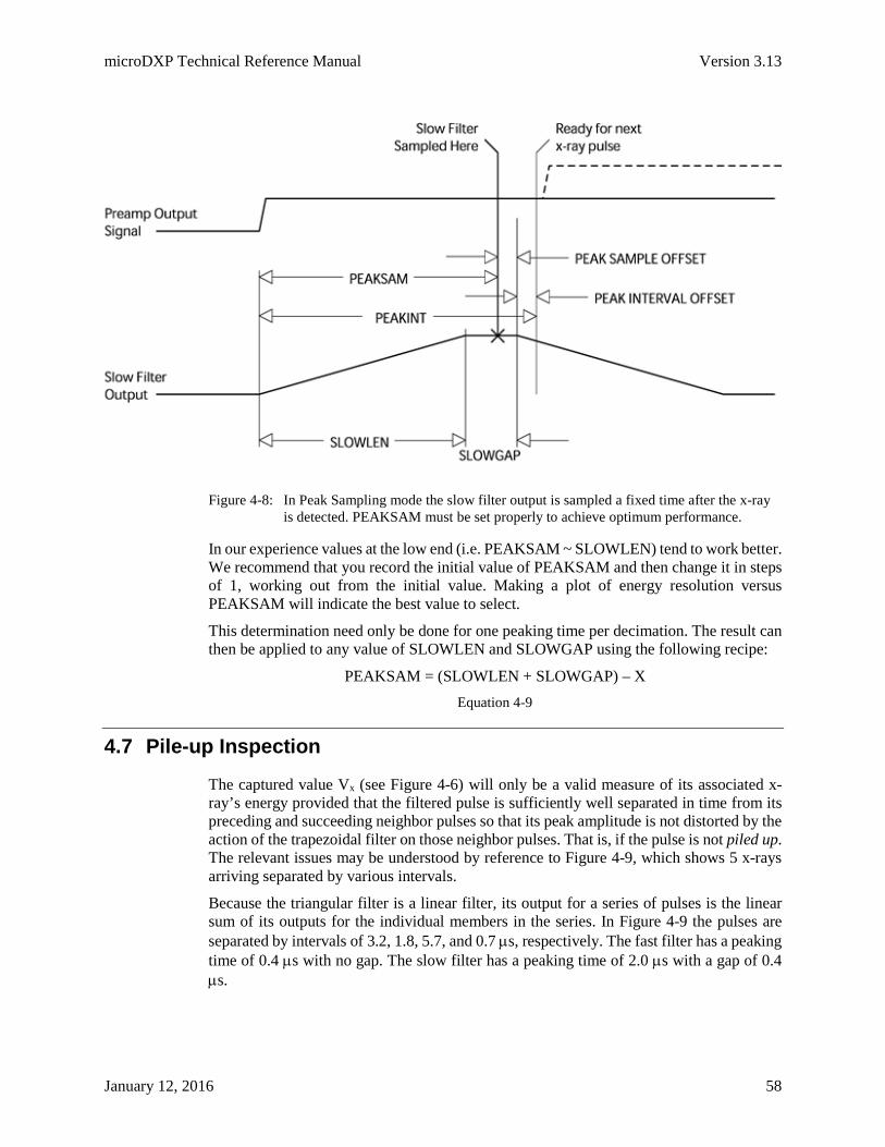
microDXP Technical Reference Manual Version 3.13
January 12, 2016 58
Figure 4-8: In Peak Sampling mode the slow filter output is sampled a fixed time after the x-ray is detected. PEAKSAM must be set properly to achieve optimum performance.
In our experience values at the low end (i.e. PEAKSAM ~ SLOWLEN) tend to work better. We recommend that you record the initial value of PEAKSAM and then change it in steps of 1, working out from the initial value. Making a plot of energy resolution versus PEAKSAM will indicate the best value to select.
This determination need only be done for one peaking time per decimation. The result can then be applied to any value of SLOWLEN and SLOWGAP using the following recipe:
PEAKSAM = (SLOWLEN + SLOWGAP) – X Equation 4-9
4.7 Pile-up Inspection
The captured value Vx (see Figure 4-6) will only be a valid measure of its associated x-ray’s energy provided that the filtered pulse is sufficiently well separated in time from its preceding and succeeding neighbor pulses so that its peak amplitude is not distorted by the action of the trapezoidal filter on those neighbor pulses. That is, if the pulse is not piled up. The relevant issues may be understood by reference to Figure 4-9, which shows 5 x-rays arriving separated by various intervals.
Because the triangular filter is a linear filter, its output for a series of pulses is the linear sum of its outputs for the individual members in the series. In Figure 4-9 the pulses are separated by intervals of 3.2, 1.8, 5.7, and 0.7 µs, respectively. The fast filter has a peaking time of 0.4 µs with no gap. The slow filter has a peaking time of 2.0 µs with a gap of 0.4 µs.
microDXP Technical Reference Manual Version 3.13
January 12, 2016 59
4.7.1 Slow Pileup The first kind of pileup is slow pileup, which refers to pileup in the slow channel. This occurs when the rising (or falling) edge of one pulse lies under the peak (specifically the sampling point) of its neighbor. Thus peaks 1 and 2 are sufficiently well separated so that the leading edge (point 2a) of peak 2 falls after the peak of pulse 1. Because the trapezoidal filter function is symmetrical, this also means that pulse 1’s trailing edge (point 1c) also does not fall under the peak of pulse 2. For this to be true, the two pulses must be separated by at least an interval of (L + G/2). Peaks 2 and 3, which are separated by only 1.8 µs, are thus seen to pileup in the present example with a 2.0 µs peaking time.
This leads to an important first point: whether pulses suffer slow pileup depends critically on the peaking time of the filter being used. The amount of pileup which occurs at a given average signal rate will increase with longer peaking times. We will quantify this in §4.10, where we discuss throughput.
Because the fast filter peaking time is only 0.4 µs, these x-ray pulses do not pileup in the fast filter channel. The DXP can therefore test for slow channel pileup by measuring for the interval PEAKINT after a pulse arrival time. If no second pulse occurs in this interval, then there is no trailing edge pileup. PEAKINT is usually set to a value close to (L + G/2 + 1). Pulse 1 passes this test, as shown in the figure. Pulse 2, however, fails the PEAKINT test because pulse 3 follows in 1.8 µs, which is less than PEAKINT = 2.3 µs. Notice, by the symmetry of the trapezoidal filter, if pulse 2 is rejected because of pulse 3, then pulse 3 is similarly rejected because of pulse 2.
Note: PEAKINT is set automatically, and there is almost never any benefit to increasing its value as it does not improve energy resolution and only decreases throughput for a given input rate.

microDXP Technical Reference Manual Version 3.13
January 12, 2016 60
Figure 4-9: A sequence of 5 x-ray pulses separated by various intervals to show the origin of both slow channel and fast channel pileup and demonstrate how the two cases are detected by the DXP.
Pulses 4 and 5 are so close together that the output of the fast filter does not fall below the threshold between them and so they are detected by the pulse detector as only being a single x-ray pulse. Indeed, only a single (though somewhat distorted) pulse emerges from the slow filter, but its peak amplitude corresponds to the energy of neither x-ray 4 nor x-ray 5. In order to reject as many of these fast channel pileup cases as possible, the DXP implements a fast channel pileup inspection test as well.
4.7.2 Fast Pileup The fast channel pileup test is based on the observation that, to the extent that the rise time of the preamplifier pulses is independent of the x-rays’ energies (which is generally the case in x-ray work except for some room temperature, compound semiconductor detectors) the base width of the fast digital filter (i.e. 2Lf + Gf) will also be energy independent and

microDXP Technical Reference Manual Version 3.13
January 12, 2016 61
will never exceed some maximum width, defined by MAXWIDTH. Thus, if the width of the fast filter output pulses is measured at threshold and found to exceed MAXWIDTH, then fast channel pileup must have occurred. This is shown graphically in Figure 4-9, where pulse 3 passes the MAXWIDTH test while the piled-up pair of pulses 4 and 5 fail the MAXWIDTH test. Thus, only pulse 1 passes both pileup inspection tests and, indeed, it is the only pulse to have a well-defined flattop region at time PEAKSAMP in the slow filter output.
MAXWIDTH should be set according to the preamplifier rise time tR and fast filter length and gap: FASTLEN and FASTGAP.
MAXWIDTH = FASTGAP + 2* FASTLEN + (tR / sampling interval) Equation 4-10
4.8 Input Count Rate (ICR) and Output Count Rate (OCR)
During data acquisition, x-rays will be absorbed in the detector at some rate. This is the input count rate, which we will refer to as ICR. Of the detected x-rays, some fraction will also satisfy pileup tests and have their values of Vx captured and placed into the spectrum. This number is the output count rate, which we refer to as the OCR. The DXP normally returns statistics in addition to the collected spectrum: the REALTIME for which data was collected; the triggering channel LIVETIME, or sum of time during which the triggering channel was below threshold (and thus ready to detect a subsequent x-ray); the FASTPEAKS, or number of times the triggering channel threshold was surmounted, and the EVTSINRUN, or number of good events captured into the spectrum. From these values, the ICR can be computed according to Equation 4-11, and the OCR according to Equation 4-12.
ICR = FASTPEAKS / LIVETIME Equation 4-11
OCR = EVTSINRUN / REALTIME Equation 4-12
Note: The fast channel LIVETIME should only be used to determine the input count rate according to Equation 4-11. Specifically, it is NOT related to the energy filter live time and should not be interpreted as the inverse of the processor deadtime. The energy filter live time can be calculated according to Equation 4-13.
Energy filter live time = REALTIME * OCR / ICR Equation 4-13
4.9 Throughput
Figure 4-10 shows how the output count rate (OCR) varies with input count rate (ICR) for a few different Peaking Times. Functionally, the OCR is seen to initially rise with increasing ICR and then saturate at higher ICR levels. The theoretical form, from Poisson statistics, for a channel that suffers from paralyzable (extending) dead time is given by:
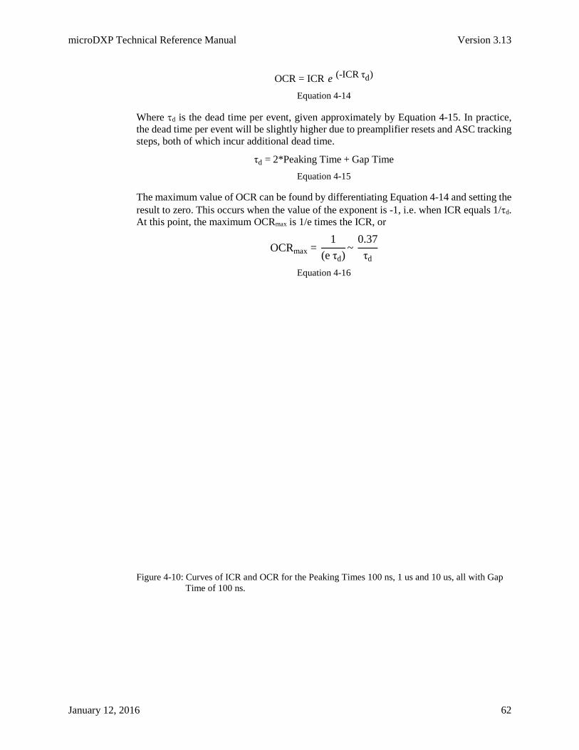
microDXP Technical Reference Manual Version 3.13
January 12, 2016 62
OCR = ICR e (-ICR τd) Equation 4-14
Where τd is the dead time per event, given approximately by Equation 4-15. In practice, the dead time per event will be slightly higher due to preamplifier resets and ASC tracking steps, both of which incur additional dead time.
τd = 2*Peaking Time + Gap Time Equation 4-15
The maximum value of OCR can be found by differentiating Equation 4-14 and setting the result to zero. This occurs when the value of the exponent is -1, i.e. when ICR equals 1/τd. At this point, the maximum OCRmax is 1/e times the ICR, or
OCRmax = 1
(e τd)~
0.37τd
Equation 4-16
Figure 4-10: Curves of ICR and OCR for the Peaking Times 100 ns, 1 us and 10 us, all with Gap Time of 100 ns.

microDXP Technical Reference Manual Version 3.13
January 12, 2016 63
Appendices
Appendix A. MicroDXP Hardware Specification
This section describes the microDXP printed circuit board dimensions, hardware settings, mounting-hole and connector locations and pinouts.
A.1 Board Dimensions and Mounting The microDXP measures 3.375” x 2.125” (as shown in Figure A-1), with 0.120” non-plated mounting holes inset by 0.175” symmetrically with respect to each of the four corners. These mounting holes are intended for use with 4-40 or equivalent screws.
A.2 Preamplifier Type Selector Switch The location of the miniature two-position slide switch S1 is displayed in Figure A-1. The two positions are silkscreen-labeled RESET and RC. Select RESET for reset-type preamplifiers. Select RC for RC-feedback preamplifiers. Note that the setting must match both your detector preamplifier and the firmware that is installed in non-volatile memory, as indicated in the Preamplifier Type field in the Detector tab. Please contact XIA if you have the wrong type of firmware installed.
A.3 Input Signal Attenuation The voltage range of the preamplifier signal must not exceed the input range of the microDXP, excluding reset transients that may exceed the range for a few microseconds. The input range is specified below in Table A-1. To accommodate preamplifiers with an output range in excess of +/-4V Volts, a finite attenuation option is included in the microDXP input circuitry. The input voltage range can be increased to +/-5.5 Volts by removing the solder from RG1 and shorting with solder the two pads of RG2 together. By default the microDXP is shipped with +/-4.0V input range, i.e. with RG1 shorted and RG2 open.
Attenuation Setting Absolute Maximum Input Voltage Input Impedance Default – 0dB Attenuation (RG1 short, RG2 open)
+/- 4.0 V 10 KΩ
Option – 2.7dB Attenuation (RG1 open, RG2 short)
+/- 5.5 V 655 Ω
Custom Customer-defined Customer-defined Table A-1: The attenuation setting determines the absolute maximum input voltage range and
input impedance
A.4 Connector Locations and Pinouts As depicted in Figures A-1 and A-2, there are three options for the input signal conductor: twisted-pair (J1), coaxial (J4) or board-to-board (J7). There are also two options for power, communications and auxiliary digital I/O, which is redundantly accessible on two separate connectors: a flat-flex cable (J12) for low and medium speed serial communications and a board-to-board connector (J11) that offers serial protocols as well as high-speed parallel access. Finally, there is a new on-board USB 2.0 option.
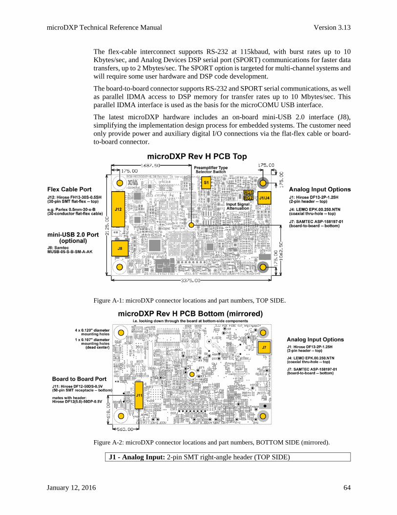
microDXP Technical Reference Manual Version 3.13
January 12, 2016 64
The flex-cable interconnect supports RS-232 at 115kbaud, with burst rates up to 10 Kbytes/sec, and Analog Devices DSP serial port (SPORT) communications for faster data transfers, up to 2 Mbytes/sec. The SPORT option is targeted for multi-channel systems and will require some user hardware and DSP code development.
The board-to-board connector supports RS-232 and SPORT serial communications, as well as parallel IDMA access to DSP memory for transfer rates up to 10 Mbytes/sec. This parallel IDMA interface is used as the basis for the microCOMU USB interface.
The latest microDXP hardware includes an on-board mini-USB 2.0 interface (J8), simplifying the implementation design process for embedded systems. The customer need only provide power and auxiliary digital I/O connections via the flat-flex cable or board-to-board connector.
Figure A-1: microDXP connector locations and part numbers, TOP SIDE.
Figure A-2: microDXP connector locations and part numbers, BOTTOM SIDE (mirrored).
J1 - Analog Input: 2-pin SMT right-angle header (TOP SIDE)

microDXP Technical Reference Manual Version 3.13
January 12, 2016 65
Hirose P/N: DF13-2P-1.25H (mating P/N: DF13-2S-1.25C; crimp contact P/N: DF13-2630SCFR) Pin # Name Description
1 SIGNAL Preamplifier output signal 2 GND Internal ground connection
Table A-2: Pin assignments for the 2-conductor SMT header analog input connection.
J4 - Analog Input: thru-hole coaxial (TOP SIDE) LEMO P/N: EPK.00.250.NTN Pin # Name Description
Center SIGNAL Preamplifier output signal Outer GND Internal ground connection
Table A-3: Pin assignments for the 2-conductor coaxial analog input connection.
J7 - Analog Input: board-to-board (BOTTOM SIDE) SAMTEC P/N: ASP-158197-01 (mating P/N: HLS-0303-G-12) Pin # Name Description
Center SIGNAL Preamplifier output signal Outer GND Internal ground connection
Table A-4: Pin assignments for the board-to-board analog input connection.
J12 – Flex Cable Port: 30-conductor, 0.5mm locking flex-cable connector; carries power, communications and auxiliary digital I/O Hirose P/N: FH12-30S-0.5SH (e.g. flat-flex cable, Parlex P/N: 0.5MM-30-x-B) Pin # Name Description
1 +AVDD Positive DC supply voltage for analog signal conditioner: Regulated +5.0V; or unregulated +5.5V if on-board regulator present.
2 -AVSS Negative DC supply voltage for analog signal conditioner: Regulated -5.0V; or unregulated -5.5V if on-board regulator present.
3 GND Internal ground connection 4 +3.3VCC +3.3V DC supply for on-board digital
components. 5 +3.3VCC +3.3V DC supply for on-board digital
components. 6 GND Internal ground connection 7 SDA I2C data line 8 SCL I2C clock 9 ExtInt* External interrupt line, active low. 10 Gate* Inhibits data acquisition, active low. 11 GND Internal ground connection 12 RX RS-232 host receive (microDXP→host) 13 TX RS-232 host transmit (host→microDXP) 14 GND Internal ground connection 15 Vprog PIC programming voltage 16 ProgData PIC programming data line

microDXP Technical Reference Manual Version 3.13
January 12, 2016 66
17 ProgClk PIC programming clock 18 Aux0 Auxiliary configurable digital I/O line: connects
to FiPPI 19 Aux1 Auxiliary configurable digital I/O line: connects
to FiPPI 20 GND Internal ground connection 21 Aux2 Auxiliary configurable digital I/O line: connects
to FiPPI 22 Aux3 Auxiliary configurable digital I/O line: connects
to FiPPI 23 +3.3VCC +3.3V DC supply for on-board digital
components. 24 SPORT_CLK DSP serial port clock line (ADSP218x SPORT) 25 GND Internal ground connection 26 SPORT_TDATA DSP serial port transmit data line (ADSP218x
SPORT) 27 SPORT_TFS DSP serial port transmit frame sync line
(ADSP218x SPORT) 28 GND Internal ground connection 29 SPORT_RDATA DSP serial port receive data line (ADSP218x
SPORT) 30 SPORT_RFS DSP serial port receive frame sync line
(ADSP218x SPORT) Table A-5: Pin assignments for the 30-conductor flat-flex interconnect
J11 – Board-to-Board Port: 50-conductor, 0.5mm mezzanine board-to-board receptacle; carries power, communications and auxiliary digital I/O Hirose P/N: DF12-50DS-0.5V (microCOMU mating header P/N: DF12(5.0)-50DP-0.5V) Pin # Name Description Odd-numbered pins (top to bottom along the right-side of the connector as shown in Figure A-2)
1 +3.3VCC +3.3V DC supply for on-board digital components.
3 +3.3VCC +3.3V DC supply for on-board digital components.
5 +3.3VCC +3.3V DC supply for on-board digital components.
7 GND Internal ground connection 9 EAD15 IDMA data/address I/O line (MSB) 11 EAD14 IDMA data/address I/O line 13 EAD13 IDMA data/address I/O line 15 EAD12 IDMA data/address I/O line 17 EAD11 IDMA data/address I/O line 19 EAD10 IDMA data/address I/O line 21 EAD9 IDMA data/address I/O line 23 EAD8 IDMA data/address I/O line 25 EAD7 IDMA data/address I/O line 27 EAD6 IDMA data/address I/O line
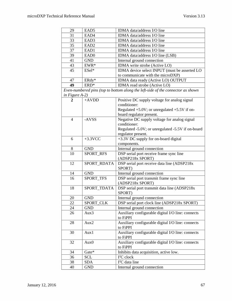
microDXP Technical Reference Manual Version 3.13
January 12, 2016 67
29 EAD5 IDMA data/address I/O line 31 EAD4 IDMA data/address I/O line 33 EAD3 IDMA data/address I/O line 35 EAD2 IDMA data/address I/O line 37 EAD1 IDMA data/address I/O line 39 EAD0 IDMA data/address I/O line (LSB) 41 GND Internal ground connection 43 EWR* IDMA write strobe (Active LO) 45 ESel* IDMA device select INPUT (must be asserted LO
to communicate with the microDXP) 47 ERdy* IDMA data ready (Active LO) OUTPUT 49 ERD* IDMA read strobe (Active LO)
Even-numbered pins (top to bottom along the left-side of the connector as shown in Figure A-2)
2 +AVDD Positive DC supply voltage for analog signal conditioner: Regulated +5.0V; or unregulated +5.5V if on-board regulator present.
4 -AVSS Negative DC supply voltage for analog signal conditioner: Regulated -5.0V; or unregulated -5.5V if on-board regulator present.
6 +3.3VCC +3.3V DC supply for on-board digital components.
8 GND Internal ground connection 10 SPORT_RFS DSP serial port receive frame sync line
(ADSP218x SPORT) 12 SPORT_RDATA DSP serial port receive data line (ADSP218x
SPORT) 14 GND Internal ground connection 16 SPORT_TFS DSP serial port transmit frame sync line
(ADSP218x SPORT) 18 SPORT_TDATA DSP serial port transmit data line (ADSP218x
SPORT) 20 GND Internal ground connection 22 SPORT_CLK DSP serial port clock line (ADSP218x SPORT) 24 GND Internal ground connection 26 Aux3 Auxiliary configurable digital I/O line: connects
to FiPPI 28 Aux2 Auxiliary configurable digital I/O line: connects
to FiPPI 30 Aux1 Auxiliary configurable digital I/O line: connects
to FiPPI 32 Aux0 Auxiliary configurable digital I/O line: connects
to FiPPI 34 Gate* Inhibits data acquisition, active low. 36 SCL I2C clock 38 SDA I2C data line 40 GND Internal ground connection

microDXP Technical Reference Manual Version 3.13
January 12, 2016 68
42 RX (B) RS-232 host receive (microDXP→host) via serial port B
44 TX (B) RS-232 host transmit (host→microDXP) via serial port B
46 GND Internal ground connection 48 EA/D* IDMA address (HI) / data (LO) selector INPUT 50 ExtInt* External interrupt line, active low.
Table A-6: Pin assignments for the 50-conductor board-to-board interconnect
A.5 Power Supplies The microDXP requires three supply voltages to operate. A supply voltage of +3.3V is used to directly power most on-board digital circuitry, with minimal LC filtering at the board entry point. On-board voltage regulators also generate other digital supply voltages. The total current requirement depends on the selected clock speed. The ripple requirements for this supply are not particularly stringent, though excessive radiated noise is to be avoided. If a switching supply is used, it should be well shielded from the microDXP.
By default, supply voltages of +/-5.5V are regulated on-board by default to generate +/-5.0V to power the analog components. This configuration tolerates ~100mV pk-pk from the switching supplies.
Voltage Range Current (max) Description +3.3V +/- 150mV 200mA Decent switching supply +5.5V to +6.0V 30mA Linear or good switching supply -5.5V to -6.0V 30mA Linear or good switching supply
Table A-7: Power supply specifications for the default microDXP assembly.
The microDXP can optionally receive +/-5.0V directly with a custom assembly build, i.e. with on-board regulators omitted. In this case either linear or very high quality switching supplies with less than 20mV pk-pk ripple/noise should be used. Contact XIA for details.
Voltage Range Current (max) Description +3.3V +/- 150mV 200mA Decent switching supply +5.0V +/- 100mV 30mA Linear or very good switching supply -5.0V +/- 100mV 30mA Linear or very good switching supply
Table A.8: Power supply specifications for the microDXP with on-board regulators omitted.
Appendix B. GLOBSET Specification
The GLOBSET is a single table of global settings. See §2.2 for details.
ID Parameter Description 0 NUMGLOBSET Number of GLOBSET parameters NOT including
NUMGLOBSET and GLOBVERSION (used internally)
1 GLOBVERSION Version of the GENSET (used internally) 2 POLARITY Preamplifier signal polarity (0: negative, 1:
positive) 3 RUNTASKS Each bit controls a separate task 4 FIPCONTROL Controls various FiPPI operations. Used for
debugging

microDXP Technical Reference Manual Version 3.13
January 12, 2016 69
5 PRESETLENLO Low word of preset run length 6 PRESETLENHI High word of preset run length 7 PRESET Preset type (0: no preset, 1: real time, 2: live time,
3: output events, 4: input events) 8 RESETINT Reset time in microseconds 9 TAURC Preamplifier RC decay time in microseconds
(unused for reset preamplifier) 10 AUTOSLEEP Auto sleep mode, as defined in command 0x46 11 SLEEPDELAY Delay before entering sleep after end run (in
seconds) 12 SLEEPMODE Manual sleep mode, as defined in command 0x47 13 STATSMODE Sets the response to the 0x06 “Read Run
Statistics” command. STATSMODE=0 (default) yields the short response (21 bytes). STATSMODE=1 yields the long response is (29 bytes, including UNDERFLOWS and OVERFLOWS).
14 WAKEDELAY Delay before exiting sleep (10 ms units)
Appendix C. GENSET Specification
Five GENSET tables each define an MCA format. See §2.3 for details.
ID Parameter Description 0 NUMGENSET Number of GENSET parameters NOT including
NUMGENSET and GENVERSION (used internally)
1 GENVERSION Version of the GENSET (used internally) 2 MCALEN Number of spectrum bins 3 MCALIMLO Lowest spectrum bin (allows offset spectrum) 4 MCALIMHI Highest spectrum bin 5 BASEBINNING Number of bins baseline values combined into
one bin in baseline histogram (power of 2) 6 BLCUT Baseline cut value, in percentage of peak value in
baseline histogram. Standard value is 5%. Expressed as x * 32768.
7 BINMULTIPLE MCA bin size in terms of the minimum. 8 BINGRANULAR Bin granularity (as defined in command 0x84: 0
== very fine, etc.) 9 GAINBASE 16-bit base gain setting. (Higher value == higher
gain). This value is modified per-peaking time by the GAINTWEAK table in the PARSET.
10 SWGAIN The discrete switched-gain value corresponding to GAINBASE
11 DGAINBASE The 16-bit unsigned mantissa of the digital fine gain trim corresponding to GAINBASE
12 DGEXPBASE The 4-bit signed exponent of the digital fine gain trim corresponding to GAINBASE
13 NUMSCA Number of active SCA windows
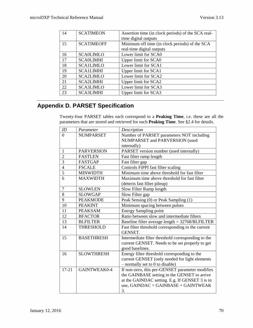
microDXP Technical Reference Manual Version 3.13
January 12, 2016 70
14 SCATIMEON Assertion time (in clock periods) of the SCA real-time digital outputs
15 SCATIMEOFF Minimum off time (in clock periods) of the SCA real-time digital outputs
16 SCA0LIMLO Lower limit for SCA0 17 SCA0LIMHI Upper limit for SCA0 18 SCA1LIMLO Lower limit for SCA1 19 SCA1LIMHI Upper limit for SCA1 20 SCA2LIMLO Lower limit for SCA2 21 SCA2LIMHI Upper limit for SCA2 22 SCA3LIMLO Lower limit for SCA3 23 SCA3LIMHI Upper limit for SCA3
Appendix D. PARSET Specification
Twenty-four PARSET tables each correspond to a Peaking Time, i.e. these are all the parameters that are stored and retrieved for each Peaking Time. See §2.4 for details.
ID Parameter Description 0 NUMPARSET Number of PARSET parameters NOT including
NUMPARSET and PARVERSION (used internally)
1 PARVERSION PARSET version number (used internally) 2 FASTLEN Fast filter ramp length 3 FASTGAP Fast filter gap 4 FSCALE Controls FiPPI fast filter scaling 5 MINWIDTH Minimum time above threshold for fast filter 6 MAXWIDTH Maximum time above threshold for fast filter
(detects fast filter pileup) 7 SLOWLEN Slow Filter Ramp length 8 SLOWGAP Slow Filter gap 9 PEAKMODE Peak Sensing (0) or Peak Sampling (1) 10 PEAKINT Minimum spacing between pulses 11 PEAKSAM Energy Sampling point 12 BFACTOR Ratio between slow and intermediate filters 13 BLFILTER Baseline filter average length = 32768/BLFILTER 14 THRESHOLD Fast filter threshold corresponding to the current
GENSET. 15 BASETHRESH Intermediate filter threshold corresponding to the
current GENSET. Needs to be set properly to get good baselines.
16 SLOWTHRESH Energy filter threshold corresponding to the current GENSET (only needed for light elements – normally set to 0 to disable)
17-21 GAINTWEAK0-4 If non-zero, this per-GENSET parameter modifies the GAINBASE setting in the GENSET to arrive at the GAINDAC setting. E.g. If GENSET 3 is in use, GAINDAC = GAINBASE + GAINTWEAK 3.

microDXP Technical Reference Manual Version 3.13
January 12, 2016 71
22-26 THRESHOLD0-4 Per-GENSET fast filter threshold values. 27-31 BASETHRESH0-4 Per-GENSET baseline filter threshold values. 32-36 SLOWTHESH0-4 Per-GENSET slow filter threshold values.
Appendix E. RS-232 Communications
This appendix describes the basic microDXP RS-232 command and response protocol. Please refer to the RS-232 Command Specification (a separate document) for a detailed presentation of all RS-232 commands.
The general structure for commands and responses is as follows: [Esc][Command][Ndata (2 bytes)][data1]…[dataN][xor CS]
Where:
Character Description [Esc] Escape (ASCII 0x1B) as a command start byte [Command] Single byte for command number, allowing up to 255
commands. See the tables below for command definitions. [Ndata] Number of data bytes to follow. Two bytes, low byte first. [data1]...[dataN] The data bytes. [xor CS] Exclusive-or checksum (bitwise xor of all bytes except for the
initial [Esc]). If the checksum is not correct an error response is returned.
Table E-1: RS-232 character definitions
The format of responses echo the format of commands; that is, they start with the [Esc]character and pass back the command # to which it is responding, followed by appropriate data and checksum. The first data byte of all responses is the return status, which is zero for a successful command. In case of an error, only the error byte is returned – no other data bytes are sent.
The command for starting a run is given below as an example:
Command:
0x1B (the escape character)
0x00 (the command)
0x01 (the low byte that sets the number of data bytes)
0x00 (the high byte that sets the number of data bytes)
0x01 (the data byte: new run, clear the data)
0x00 (bitwise XOR—excludes escape character)
Response (if successful):
0x1B (the escape character)
0x00 (the command is always returned)
0x03 (the low byte that sets the number of data bytes)
0x00 (the high byte that sets the number of data bytes)
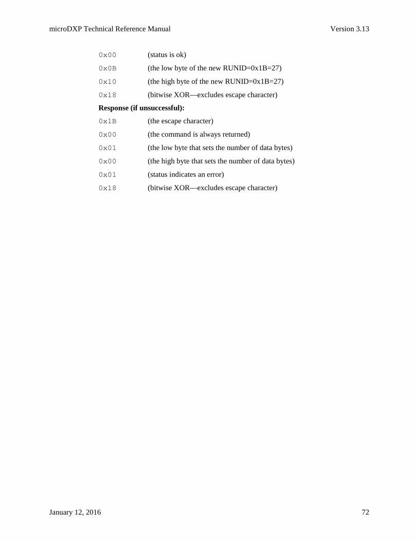
microDXP Technical Reference Manual Version 3.13
January 12, 2016 72
0x00 (status is ok)
0x0B (the low byte of the new RUNID=0x1B=27)
0x10 (the high byte of the new RUNID=0x1B=27)
0x18 (bitwise XOR—excludes escape character)
Response (if unsuccessful):
0x1B (the escape character)
0x00 (the command is always returned)
0x01 (the low byte that sets the number of data bytes)
0x00 (the high byte that sets the number of data bytes)
0x01 (status indicates an error)
0x18 (bitwise XOR—excludes escape character)