micro- and nano-technology - uni-jena.deand+nano_technol… · u.d. zeitner fraunhofer institut...
TRANSCRIPT

U.D. ZeitnerFraunhofer Institut für Angewandte Optik und Feinmechanik
Jena
Micro- and Nano-Technology...... for Optics
Today: 1. Introduction
E. – Bernhard KleyInstitute of Applied Physics Friedrich-Schiller University Jena
and
Fraunhofer Institut für Angewandte Optik und Feinmechanik Jena

Course Content
1. Introduction (today)
2. Basic optical considerations
- discussion of physical effects relevant in micro- and nano-optics
3. Fabrication technologies for micro- and nano-structures
- Coating technologies
- Lithography
- Etching technologies
- Replication
- Ultra-precision micro-machining
4. Characterization techniques
- mechanical profiler
- AFM
- SEM
- optical surface profiler
- interferometer
5. Applications

Additional Information
Literature:
- S. Sinzinger, J. Jahns “Microoptics”, Wiley-VCH
- H.-P. Herzig “Micro-Optics”, Taylor & Francis
- B.C. Kress, P. Meyrueis “Applied Digital Optics”, Wiley
- C. Mack “Fundamental Principles of Optical Lithography”, Wiley
Course material will be uploaded to:
www.iap.uni-jena.de/teaching.html
Lecture “Micro- and Nano-Technology”

Micro-Structured Optics in Nature
2µm
Nano-structures with
anti-reflection
properties on moth‘s-
eyes
Lens-arrays as
insects eyes
100µm
Colors of butterflies
by diffraction
gratings
4µm

Different Approaches
Nature Technology
!?
“Bottom-Up” “Top-Down”
Lithography

Modern and high end optics need
micro- und nanostructures
2 prominent examples

Galaxies are very differentand what about our milky way ?
Vigo Galaxy clusterAbout 150 galaxies visible in the picture

NGC 6744
GAIA (ESA)
launched in Dec. 2013
RVS
230mm
GAIA’s effective medium
grating

Spectrometer grating for the Gaia mission
of European Space Agency
Gaia (Dec. 2011)
-1E9 Stars
- Magnitude: 22.5-20
Distance measurement by read shift measurement
Radial Velocity Spectrometer
Spektral range: 847-874 nm
Grating

Gravitational Waves
Gravitational wave Astronomy
1916 General Theory of Relativity[Einstein, AdP 1916]
[www.nikhef.nl]
relative length deviation:

Reflective Michelson-Interferometer and critical components
[Drever, Proc. 7th M. Grossmann Meeting 1996]
Gravitational Wave Detection
Dl
How to reduce the
thermas noise
Detector

nH
nL
nH
nHnL
Motivation: Cavities for interferometer in gravitational detection and lasers
Low optical and mechanical loss is required
high mechanical Q-factor
low reflectivity
quartz / silicon
nH
nL
Monolithic dielectric mirror
high reflectivity
low mechanical Q-factor
Does a monolithic solution exist?

Monolithic resonant Si-mirror (=1550 nm)
Si
waveguide + grating
grating/effective media
Si
99.8% reflectivity
measured @ 1550nm

Silicon-Pattern for Monolithic Mirrors

huge variety of low and high resolution structures
Examples of micro-structured elements

1mm
1µm
10nm
10µm
100µm
100nm
characteristic
feature size
micro-lenses, micro-prisms
lens-arrays,
refractive beam-shaper
diffractive beam-shaper,
Fresnel-lenses,
diffraction gratings
effective media,
sub--gratings,
photonic crystals,
meta-materials
hybride elements
Size scale of micro-optical effects

Size-Scale of Optical Structures
1Å
1nm
1µm
1mm
1m
law of refraction
and reflection
light diffraction
effective medium
spontaneous and
stimulated emission
astronomic
mirrors
lenses
micro-lenses
antireflection pattern,
polarizers, phase retarder
photonic crystals
miniaturized
lenses
paraxial beam splitters
non paraxial beam splitter
spectroscopic gratingsm
icro
op
tics
(atomic size) light sources
optical elementsoptical effects

Effects of Size-Scaling
1mm 100µm 10µm 1µm 100nm
refraction diffraction
influence of physical effects on optical functions
is changing if characteristic feature sizes are scaled
focus:f=5mm
125µ
m
structure size
artificial
dichroitic
materials
physical effect:effective material-
propertiesdisturbing useful !
diffractive
beam splitter
2µm
wire-
grid-
polarizer

Milestones of optical engineering
Maxwell
1831 - 1879
electromagnetic
wave theory
Fresnel
1788 - 1827
wave theory
of the light
Hertz
1857 - 1894
exp. confirm.
of Maxwell
Fourier
1768 - 1830
Fourier
expansion
Abbe
1840 - 1905
theory of
opt. image
Basics in physics
and mathematicsAnalytical and numerical
evaluation of physical optics
Personal
Computer
Dedicated
micro- and
nanomachining
technologies
18
00
19
00
20
00
Fundamental
understanding
of optics
Zuse
1910 - 1995
1941
1st calculator

Fabrication Technologies for Micro-Optics
common micro-optics fabrication methods are
• lithography (photo-, e-beam-, laser-)
• ultra precision micro-machining
• melting / reflow technology
• more elaborated technologies
different size and functionality
different fabrication methods
for micro-optical components compared to classical (macro) optics

4. Resist exposure
e-beam lithography
or photolithography
Lithography Process Chain for Resist pattern
5. Resist development
resist
(sensitive to light or
electrons)
Substrate
(e.g. Si-wafer)
, e-
1. Substrate preparation
(cleaning, …)
2. Resist coating
(e.g. spin coating)
patterned resist
mask for
subsequent
processes
evaporation of
solvent
3. Baking

High-End Lithography Tool
DUV lithography stepper, =193nm
(ASML)
very low flexibility
EUV lithography stepper, =13.5nm
(ASML)
microelectronic chips
on Si-wafers
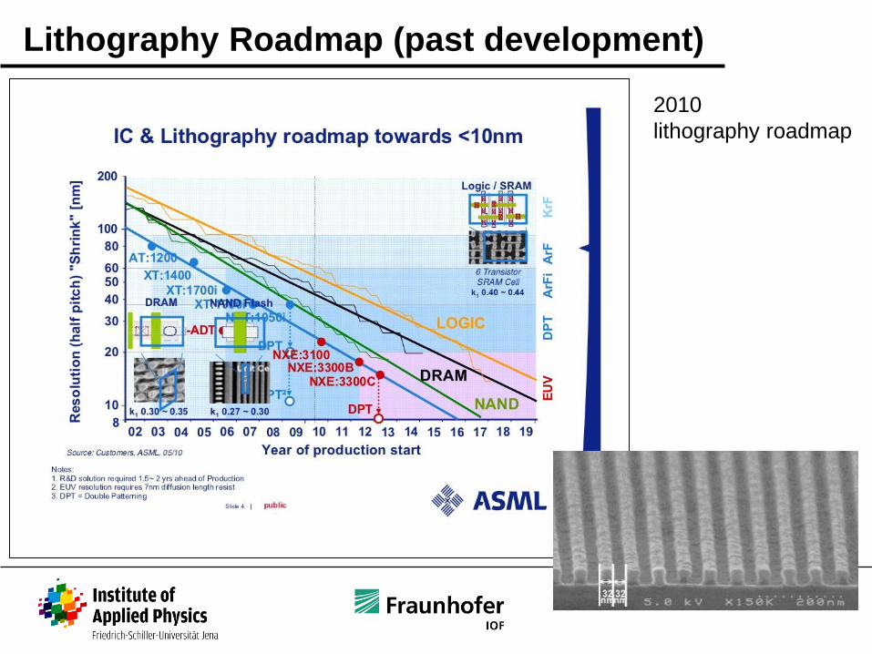
Lithography Roadmap (past development)
2010
lithography roadmap

Lithography Roadmap (ongoing)
International Technology Roadmap for Semiconductors (2015)

Lithography for Optical Applications
Lithography tools are developed for micro-electronics fabrication!
Demands of optics on lithography:
• arbitrary lateral contours (often radially symmetric)
• several 100mm size of single elements with sub-micron features
• thick substrates for elements with low wave-front error
• non-planar substrates possible
• …
steady development along
semiconductor road-mapvanishing versatility for
other applications

Typical Optical Surfaces and Contours
Contours Profiles
lens prism beam shaper
binary grating blazed grating
subwavelength gratings
complex surface
profiles
>>
<
>
>>
>
<
characteristic
detail
Courtesy of E.-B. Kley

Demanding Micro Optics Applications
Computer-Generated Holograms
Pulse compression gratings
Spectrometry for Space Applications
Polarizers

1. Resist exposure with
e-beam lithography
Lithography Process Chain for Optics
2. Resist development
3. Chromium etching
(RIE)
4. Deep etching into
substrate (ICP)
resist
Cr-layer
SiO2-Substrate
e-
optional:
multiple iterations
of the process for
multi-level elements

Technology for continuous profiles
variable dose exposure:
development:
resist
substrate
intensity modulated
exposure beam
t1 t2
dose dependent profile depth in
resist after development process
proportional transfer (RIE):
Ions (e.g. CF4)
element profile transferred
into substrate material