mhs2060at, mhs2040at mhs2030at, mhs2020at disk drives ... … · mhs2060at, mhs2040at mhs2030at,...
TRANSCRIPT

C141-E171-03EN
MHS2060AT, MHS2040ATMHS2030AT, MHS2020AT
DISK DRIVES
PRODUCT MANUAL

FOR SAFE OPERATIONHandling of This Manual
This manual contains important information for using this product. Read thoroughly before usingthe product. Use this product only after thoroughly reading and understanding especially thesection “Important Alert Items” in this manual. Keep this manual handy, and keep it carefully.
FUJITSU makes every effort to prevent users and bystanders from being injured or from sufferingdamage to their property. Use the product according to this manual.
IMPORTANT NOTE TO USERS
READ THE ENTIRE MANUAL CAREFULLY BEFORE USING THIS PRODUCT.INCORRECT USE OF THE PRODUCT MAY RESULT IN INJURY OR DAMAGE TOUSERS, BYSTANDERS OR PROPERTY.
While FUJITSU has sought to ensure the accuracy of all information in this manual, FUJITSUassumes no liability to any party for any damage caused by any error or omission contained in thismanual, its updates or supplements, whether such errors or omissions result from negligence,accident, or any other cause. In addition, FUJITSU assumes no liability with respect to theapplication or use of any product or system in accordance with the descriptions or instructionscontained herein; including any liability for incidental or consequential damages arising therefrom.FUJITSU DISCLAIMS ALL WARRANTIES REGARDING THE INFORMATIONCONTAINED HEREIN, WHETHER EXPRESSED, IMPLIED, OR STATUTORY.
FUJITSU reserves the right to make changes to any products described herein without furthernotice and without obligation.
This product is designed and manufactured for use in standard applications such as office work,personal devices and household appliances. This product is not intended for special uses (atomiccontrols, aeronautic or space systems, mass transport vehicle operating controls, medical devicesfor life support, or weapons firing controls) where particularly high reliability requirements exist,where the pertinent levels of safety are not guaranteed, or where a failure or operational error couldthreaten a life or cause a physical injury (hereafter referred to as "mission-critical" use). Customersconsidering the use of these products for mission-critical applications must have safety-assurancemeasures in place beforehand. Moreover, they are requested to consult our sales representativebefore embarking on such specialized use.
The contents of this manual may be revised without prior notice.
The contents of this manual shall not be disclosed in any way or reproduced in any media withoutthe express written permission of Fujitsu Limited.
All Rights Reserved, Copyright FUJITSU LIMITED 2002

C141-E171-03EN
Revision History
(1/1)
Edition Date Revised section (*1)(Added/Deleted/Altered)
Details
01 2002-07-12
02 2002-07-31
03 2002-09-20
*1 Section(s) with asterisk (*) refer to the previous edition when those were deleted.

This page is intentionally left blank.

C141-E171-03EN i
Preface
This manual describes the MHS Series, 2.5-inch hard disk drives. These driveshave a built-in controller that is compatible with the ATA interface.
This manual describes the specifications and functions of the drives and explainsin detail how to incorporate the drives into user systems. This manual assumesthat the reader has a basic knowledge of hard disk drives and theirimplementations in computer systems.
This manual consists of seven chapters and sections explaining the specialterminology and abbreviations used in this manual:
Overview of Manual
CHAPTER 1 Device Overview
This chapter gives an overview of the MHS Series and describes their features.
CHAPTER 2 Device Configuration
This chapter describes the internal configurations of the MHS Series and theconfiguration of the systems in which they operate.
CHAPTER 3 Installation Conditions
This chapter describes the external dimensions, installation conditions, and switchsettings of the MHS Series.
CHAPTER 4 Theory of Device Operation
This chapter describes the operation theory of the MHS Series.
CHAPTER 5 Interface
This chapter describes the interface specifications of the MHS Series.
CHAPTER 6 Operations
This chapter describes the operations of the MHS Series.
Glossary
The glossary describes the technical terms that need to be understood to read thismanual.
Acronyms and Abbreviations
This section gives the meanings of the definitions used in this manual.

Preface
ii C141-E171-03EN
Conventions for Alert Messages
This manual uses the following conventions to show the alert messages. An alertmessage consists of an alert signal and alert statements. The alert signal consistsof an alert symbol and a signal word or just a signal word.
The following are the alert signals and their meanings:
This indicates a hazardous situation could result inminor or moderate personal injury if the user doesnot perform the procedure correctly. This alertsignal also indicates that damages to the product orother property may occur if the user does not performthe procedure correctly.
This indicates information that could help the useruse the product more efficiently.
In the text, the alert signal is centered, followed below by the indented message.A wider line space precedes and follows the alert message to show where the alertmessage begins and ends. The following is an example:
(Example)
Data corruption: Avoid mounting the disk drive near strongmagnetic sources such as loud speakers. Ensure that the disk driveis not affected by external magnetic fields.
The main alert messages in the text are also listed in the “Important Alert Items.”
Operating Environment
This product is designed to be used in offices or computer rooms.
Conventions
An MHS-series device is sometimes simply referred to as a "hard disk drive,""HDD," "drive," or "device" in this document.
Decimal numbers are represented normally.
Hexadecimal numbers are represented as shown in the following examples:X'17B9', 17B9h, 17B9H, or 17B9H.
Binary numbers are represented as shown in the following examples: 010 or010b.

Preface
C141-E171-03EN iii
Attention
Please forward any comments you may have regarding this manual.
To make this manual easier for users to understand, opinions from readers areneeded. Please write your opinions or requests on the Comment at the back ofthis manual and forward it to the address described in the sheet.
Liability Exception
“Disk drive defects” refers to defects that involve adjustment, repair, orreplacement.
Fujitsu is not liable for any other disk drive defects, such as those caused by usermisoperation or mishandling, inappropriate operating environments, defects in thepower supply or cable, problems of the host system, or other causes outside thedisk drive.

This page is intentionally left blank.

C141-E171-03EN v
Important Alert Items
Important Alert Messages
The important alert messages in this manual are as follows:
A hazardous situation could result in minor or moderate personalinjury if the user does not perform the procedure correctly. Also,damage to the product or other property, may occur if the user does notperform the procedure correctly.
Task Alert message Page
Normal Operation Data corruption: Avoid mounting the disk near strongmagnetic sources such as loud speakers. Ensure that the diskdrive is not affected by external magnetic fields.Damage: Do not press the cover of the disk drive. Pressingit too hard, the cover and the spindle motor contact, whichmay cause damage to the disk drive.
Static: When handling the device, disconnect the bodyground (500 kΩ or greater). Do not touch the printed circuitboard, but hold it by the edges.
3-7

This page is intentionally left blank.

C141-E171-03EN vii
Manual Organization
MHS2060AT, MHS2040ATMHS2030AT, MHS2020AT
DISK DRIVESPRODUCT MANUAL
(C141-E171)
<This manual>
• Device Overview• Device Configuration• Installation Conditions• Theory of Device Operation• Interface• Operations
MHS2060AT, MHS2040ATMHS2030AT, MHS2020AT
DISK DRIVESMAINTENANCE MANUAL
(C141-F059)
• Maintenance and Diagnosis• Removal and Replacement Procedure

This page is intentionally left blank.

C141-E171-03EN ix
Contents
Device Overview .................................................................................................1-1
1.1 Features ...................................................................................................1-2
1.1.1 Functions and performance ...................................................................1-2
1.1.2 Adaptability...........................................................................................1-2
1.1.3 Interface.................................................................................................1-3
1.2 Device Specifications..............................................................................1-4
1.2.1 Specifications summary ........................................................................1-4
1.2.2 Model and product number ...................................................................1-5
1.3 Power Requirements ...............................................................................1-5
1.4 Environmental Specifications .................................................................1-8
1.5 Acoustic Noise ........................................................................................1-9
1.6 Shock and Vibration................................................................................1-9
1.7 Reliability..............................................................................................1-10
1.8 Error Rate ..............................................................................................1-11
1.9 Media Defects .......................................................................................1-11
1.10 Load/Unload Function ..........................................................................1-11
1.11 Advanced Power Management..............................................................1-12
CHAPTER 2 Device Configuration ................................................................2-1
2.1 Device Configuration ..............................................................................2-2
2.2 System Configuration..............................................................................2-4
2.2.1 ATA interface .......................................................................................2-4
2.2.2 1 drive connection .................................................................................2-4
2.2.3 2 drives connection ...............................................................................2-4

Contents
x C141-E171-03EN
CHAPTER 3 Installation Conditions ............................................................. 3-1
3.1 Dimensions ..............................................................................................3-2
3.2 Mounting .................................................................................................3-3
3.3 Cable Connections...................................................................................3-9
3.3.1 Device connector ...................................................................................3-9
3.3.2 Cable connector specifications............................................................3-10
3.3.3 Device connection ...............................................................................3-10
3.3.4 Power supply connector (CN1) ...........................................................3-11
3.4 Jumper Settings .....................................................................................3-11
3.4.1 Location of setting jumpers.................................................................3-11
3.4.2 Factory default setting.........................................................................3-12
3.4.3 Master drive-slave drive setting ..........................................................3-12
3.4.4 CSEL setting........................................................................................3-13
3.4.5 Power Up in Standby setting ...............................................................3-14
CHAPTER 4 Theory of Device Operation ..................................................... 4-1
4.1 Outline .....................................................................................................4-2
4.2 Subassemblies..........................................................................................4-2
4.2.1 Disk........................................................................................................4-2
4.2.2 Head.......................................................................................................4-2
4.2.3 Spindle...................................................................................................4-3
4.2.4 Actuator .................................................................................................4-3
4.2.5 Air filter.................................................................................................4-3
4.3 Circuit Configuration ..............................................................................4-4
4.4 Power-on Sequence .................................................................................4-7
4.5 Self-calibration ........................................................................................4-8
4.5.1 Self-calibration contents........................................................................4-8
4.5.2 Execution timing of self-calibration......................................................4-9
4.5.3 Command processing during self-calibration......................................4-10
4.6 Read/write Circuit .................................................................................4-10

Contents
C141-E171-03EN xi
4.6.1 Read/write preamplifier (HDIC) .........................................................4-10
4.6.2 Write circuit ........................................................................................4-10
4.6.3 Read circuit .........................................................................................4-12
4.6.4 Digital PLL circuit ..............................................................................4-13
4.7 Servo Control ........................................................................................4-14
4.7.1 Servo control circuit............................................................................4-14
4.7.2 Data-surface servo format ...................................................................4-17
4.7.3 Servo frame format..............................................................................4-19
4.7.4 Actuator motor control........................................................................4-20
4.7.5 Spindle motor control..........................................................................4-21
CHAPTER 5 Interface .....................................................................................5-1
5.1 Physical Interface ....................................................................................5-2
5.1.1 Interface signals ....................................................................................5-2
5.1.2 Signal assignment on the connector......................................................5-3
5.2 Logical Interface .....................................................................................5-6
5.2.1 I/O registers ...........................................................................................5-7
5.2.2 Command block registers......................................................................5-8
5.2.3 Control block registers ........................................................................5-13
5.3 Host Commands ....................................................................................5-14
5.3.1 Command code and parameters ..........................................................5-14
5.3.2 Command descriptions........................................................................5-18
5.3.3 Error posting......................................................................................5-104
5.4 Command Protocol..............................................................................5-106
5.4.1 PIO Data transferring commands from device to host ......................5-106
5.4.2 PIO Data transferring commands from host to device......................5-108
5.4.3 Commands without data transfer ......................................................5-110
5.4.4 Other commands ...............................................................................5-112
5.4.5 DMA data transfer commands ..........................................................5-112
5.5 Ultra DMA Feature Set .......................................................................5-115
5.5.1 Overview ...........................................................................................5-115
5.5.2 Phases of operation ...........................................................................5-116

Contents
xii C141-E171-03EN
5.5.3 Ultra DMA data in commands ..........................................................5-116
5.5.3.1 Initiating an Ultra DMA data in burst .............................................5-116
5.5.3.2 The data in transfer..........................................................................5-117
5.5.3.3 Pausing an Ultra DMA data in burst ...............................................5-117
5.5.3.4 Terminating an Ultra DMA data in burst ........................................5-118
5.5.4 Ultra DMA data out commands ........................................................5-121
5.5.4.1 Initiating an Ultra DMA data out burst ...........................................5-121
5.5.4.2 The data out transfer........................................................................5-121
5.5.4.3 Pausing an Ultra DMA data out burst .............................................5-122
5.5.4.4 Terminating an Ultra DMA data out burst ......................................5-123
5.5.5 Ultra DMA CRC rules.......................................................................5-125
5.5.6 Series termination required for Ultra DMA ......................................5-126
5.6 Timing .................................................................................................5-127
5.6.1 PIO data transfer................................................................................5-127
5.6.2 Multiword data transfer.....................................................................5-128
5.6.3 Ultra DMA data transfer ...................................................................5-129
5.6.3.1 Initiating an Ultra DMA data in burst .............................................5-129
5.6.3.2 Ultra DMA data burst timing requirements ....................................5-130
5.6.3.3 Sustained Ultra DMA data in burst .................................................5-133
5.6.3.4 Host pausing an Ultra DMA data in burst.......................................5-134
5.6.3.5 Device terminating an Ultra DMA data in burst .............................5-135
5.6.3.6 Host terminating an Ultra DMA data in burst.................................5-136
5.6.3.7 Initiating an Ultra DMA data out burst ...........................................5-137
5.6.3.8 Sustained Ultra DMA data out burst ...............................................5-138
5.6.3.9 Device pausing an Ultra DMA data out burst .................................5-139
5.6.3.10 Host terminating an Ultra DMA data out burst...............................5-140
5.6.3.11 Device terminating an Ultra DMA data out burst ...........................5-141
5.6.4 Power-on and reset ............................................................................5-142
CHAPTER 6 Operations................................................................................. 6-1
6.1 Device Response to the Reset .................................................................6-2
6.1.1 Response to power-on ...........................................................................6-2
6.1.2 Response to hardware reset ...................................................................6-3
6.1.3 Response to software reset ....................................................................6-5

Contents
C141-E171-03EN xiii
6.1.4 Response to diagnostic command .........................................................6-6
6.2 Power Save..............................................................................................6-7
6.2.1 Power save mode...................................................................................6-7
6.2.2 Power commands ..................................................................................6-9
6.3 Defect Processing....................................................................................6-9
6.3.1 Spare area ..............................................................................................6-9
6.3.2 Alternating processing for defective sectors.......................................6-10
6.4 Read-ahead Cache .................................................................................6-12
6.4.1 Data buffer structure ...........................................................................6-12
6.4.2 Caching operation ...............................................................................6-12
6.4.3 Using the read segment buffer ............................................................6-15
6.4.3.1 Miss-hit (no hit) ................................................................................6-15
6.4.3.2 Sequential reading.............................................................................6-16
6.4.3.3 Full hit ...............................................................................................6-18
6.4.3.4 Partial hit ...........................................................................................6-19
6.5 Write Cache...........................................................................................6-20
6.5.1 Caching operation ...............................................................................6-20
Glossary ...........................................................................................................GL-1
Acronyms and Abbreviations.........................................................................AB-1
Index ................................................................................................................. IN-1

Contents
xiv C141-E171-03EN
Illustrations
Figures
Figure 1.1 Negative voltage at +5V when power is turned off ...........................1-6
Figure 1.2 Current fluctuation (Typ.) at +5V when power is turned on .............1-8
Figure 2.1 Disk drive outerview ..........................................................................2-2
Figure 2.2 Configuration of disk media heads.....................................................2-3
Figure 2.3 1 drive system configuration ..............................................................2-4
Figure 2.4 2 drives configuration.........................................................................2-4
Figure 3.1 Dimensions.........................................................................................3-2
Figure 3.2 Orientation..........................................................................................3-3
Figure 3.3 Mounting frame structure...................................................................3-4
Figure 3.4 Location of breather ...........................................................................3-5
Figure 3.5 Surface temperature measurement points ..........................................3-6
Figure 3.6 Service area ........................................................................................3-7
Figure 3.7 Handling cautions...............................................................................3-8
Figure 3.8 Connector locations............................................................................3-9
Figure 3.9 Cable connections ............................................................................3-10
Figure 3.10 Power supply connector pins (CN1).................................................3-11
Figure 3.11 Jumper location.................................................................................3-11
Figure 3.12 Factory default setting ......................................................................3-12
Figure 3.13 Jumper setting of master or slave drive ............................................3-12
Figure 3.14 CSEL setting.....................................................................................3-13
Figure 3.15 Example (1) of Cable Select .............................................................3-13
Figure 3.16 Example (2) of Cable Select .............................................................3-14
Figure 4.1 Head structure ....................................................................................4-3
Figure 4.2 Power Supply Configuration ..............................................................4-5
Figure 4.3 Circuit Configuration .........................................................................4-6
Figure 4.4 Power-on operation sequence.............................................................4-8
Figure 4.5 Read/write circuit block diagram .....................................................4-11
Figure 4.6 Frequency characteristic of programmable filter .............................4-12
Figure 4.7 Block diagram of servo control circuit.............................................4-14
Figure 4.8 Physical sector servo configuration on disk surface ........................4-18
Figure 4.9 Servo frame format...........................................................................4-19

Contents
C141-E171-03EN xv
Figure 5.1 Interface signals....................................................................................5-2
Figure 5.2 Execution example of READ MULTIPLE command .....................5-21
Figure 5.3 Read Sector(s) command protocol .................................................5-107
Figure 5.4 Protocol for command abort ..........................................................5-108
Figure 5.5 WRITE SECTOR(S) command protocol.......................................5-110
Figure 5.6 Protocol for the command execution without data transfer ...........5-111
Figure 5.7 Normal DMA data transfer ............................................................5-114
Figure 5.8 Ultra DMA termination with pull-up or pull-down .......................5-126
Figure 5.9 PIO data transfer timing ...................................................................5-127
Figure 5.10 Multiword DMA data transfer timing (mode 2).............................5-128
Figure 5.11 Initiating an Ultra DMA data in burst ............................................5-129
Figure 5.12 Sustained Ultra DMA data in burst ................................................5-133
Figure 5.13 Host pausing an Ultra DMA data in burst ......................................5-134
Figure 5.14 Device terminating an Ultra DMA data in burst ............................5-135
Figure 5.15 Host terminating an Ultra DMA data in burst ................................5-136
Figure 5.16 Initiating an Ultra DMA data out burst ..........................................5-137
Figure 5.17 Sustained Ultra DMA data out burst ..............................................5-138
Figure 5.18 Device pausing an Ultra DMA data out burst ................................5-139
Figure 5.19 Host terminating an Ultra DMA data out burst ..............................5-140
Figure 5.20 Device terminating an Ultra DMA data out burst ..........................5-141
Figure 6.1 Response to power-on ..........................................................................6-3
Figure 6.2 Response to hardware reset ..................................................................6-4
Figure 6.3 Response to software reset ...................................................................6-5
Figure 6.4 Response to diagnostic command.........................................................6-6
Figure 6.5 Sector slip processing.........................................................................6-10
Figure 6.6 Alternate cylinder assignment processing..........................................6-11
Figure 6.7 Data buffer structure...........................................................................6-12

Contents
xvi C141-E171-03EN
Tables
Table 1.1 Specifications .....................................................................................1-4
Table 1.2 Model names and product numbers....................................................1-5
Table 1.3 Current and power dissipation ...........................................................1-7
Table 1.4 Environmental specifications .............................................................1-8
Table 1.5 Acoustic noise specification...............................................................1-9
Table 1.6 Shock and vibration specification ......................................................1-9
Table 3.1 Surface temperature measurement points and standard values..........3-6
Table 3.2 Cable connector specifications.........................................................3-10
Table 5.1 Signal assignment on the interface connector ....................................5-3
Table 5.2 I/O registers ........................................................................................5-7
Table 5.3 Command code and parameters........................................................5-15
Table 5.4 Information to be read by IDENTIFY DEVICE command .............5-34
Table 5.5 Features register values and settable modes.....................................5-44
Table 5.6 Diagnostic code ................................................................................5-56
Table 5.7 Features Register values (subcommands) and functions..................5-68
Table 5.8 Format of device attribute value data...............................................5-72
Table 5.9 Format of insurance failure threshold value data.............................5-72
Table 5.10 Log Directory Data Format...............................................................5-77
Table 5.11 Data format of SMART Summary Error Log ...................................5-78
Table 5.11.1 Data format of SMART Comprehensive Error Log ......................5-79
Table 5.12 SMART self test log data format ......................................................5-80
Table 5.13 Contents of security password..........................................................5-82
Table 5.14 Contents of SECURITY SET PASSWORD data ............................5-86
Table 5.15 Relationship between combination of Identifier andSecurity level, and operation of the lock function ...........................5-87
Table 5.16 DEVICE CONFIGURATION IDENTIFY data structure .................5-93
Table 5.17 Command code and parameters .....................................................5-104
Table 5.18 Ultra DMA data burst timing requirements .....................................5-130
Table 5.19 Ultra DMA sender and recipient timing requirements ....................5-132

C141-E171-03EN 1-1
CHAPTER 1 Device Overview
1.1 Features
1.2 Device Specifications
1.3 Power Requirements
1.4 Environmental Specifications
1.5 Acoustic Noise
1.6 Shock and Vibration
1.7 Reliability
1.8 Error Rate
1.9 Media Defects
1.10 Load/Unload Function
1.11 Advanced Power Management
Overview and features are described in this chapter, and specifications and powerrequirement are described.
The MHS Series are 2.5-inch hard disk drives with built-in disk controllers.These disk drives use the AT-bus hard disk interface protocol and are compactand reliable.

Device Overview
1-2 C141-E171-03EN
1.1 Features
1.1.1 Functions and performance
The following features of the MHS Series are described.
(1) Compact
The MHS Series has 1 disk or 2 disks of 65 mm (2.5 inches) diameter, and itsheight is 9.5 mm (0.374 inch).
(2) Large capacity
The disk drive can record up to 30 GB (formatted) on one disk using the 48/50RLL recording method and 30 recording zone technology. The MHS Series has aformatted capacity of 60 GB (MHS2060AT), 40 GB (MHS2040AT), 30 GB(MHS2030AT) and 20 GB (MHS2020AT) respectively.
(3) High-speed Transfer rate
The disk drives (the MHS Series) have an internal data rate up to 38.1 MB/s. Thedisk drive supports an external data rate up to 100 MB/s (U-DMA mode 5).
(4) Average positioning time
Use of a rotary voice coil motor in the head positioning mechanism greatlyincreases the positioning speed. The average positioning time is 12 ms (at read).
1.1.2 Adaptability
(1) Power save mode
The power save mode feature for idle operation, stand by and sleep modes makesThe disk drives (the MHS Series) ideal for applications where power consumptionis a factor.
(2) Wide temperature range
The disk drives (the MHS Series) can be used over a wide temperature range(5°C to 55°C).
(3) Low noise and vibration
In Ready status, the noise of the disk drives (the MHS Series) is only 24 dBA(measured at 0.3 m apart from the drive under the idle mode).
(4) High resistance against shock
The Load/Unload mechanism is highly resistant against non-operation shock upto 8820 m/s2 (900G).

1.1 Features
C141-E171-03EN 1-3
1.1.3 Interface
(1) Connection to ATA interface
The MHS-series disk drives have built-in controllers compatible with the ATAinterface.
(2) 2 MB data buffer
The disk drives (the MHS Series) use a 2 MB data buffer to transfer data betweenthe host and the disk media.
In combination with the read-ahead cache system described in item (3) and thewrite cache described in item (7), the buffer contributes to efficient I/Oprocessing.
(3) Read-ahead cache system
After the execution of a disk read command, the disk drive automatically readsthe subsequent data block and writes it to the data buffer (read ahead operation).This cache system enables fast data access. The next disk read command wouldnormally cause another disk access. But, if the read ahead data corresponds to thedata requested by the next read command, the data in the buffer can be transferredinstead.
(4) Master/slave
The disk drives (the MHS Series) can be connected to ATA interface as daisychain configuration. Drive 0 is a master device, drive 1 is a slave device.
(5) Error correction and retry by ECC
If a recoverable error occurs, the disk drives (the MHS Series) themselves attempterror recovery. The ECC has improved buffer error correction for correctabledata errors.
(6) Self-diagnosis
The disk drives (the MHS Series) have a diagnostic function to check operation ofthe controller and disk drives. Executing a diagnostic function of the smartcommand invokes self-diagnosis.
(7) Write cache
When the disk drives (the MHS Series) receive a write command, the disk drivespost the command completion at completion of transferring data to the data buffercompletion of writing to the disk media. This feature reduces the access time atwriting.

Device Overview
1-4 C141-E171-03EN
1.2 Device Specifications
1.2.1 Specifications summary
Table 1.1 shows the specifications of the disk drives (MHS Series).
Table 1.1 Specifications (1/2)
MHS2060AT MHS2040AT MHS2030AT MHS2020AT
Format Capacity (*1) 60 GB 40 GB 30 GB 20 GB
Number of Heads 4 3 2 2
Number of Cylinders (User) 47104 47104 47104 35264
Number of Sectors (User) 117,210,240 78,140,160 58,605,120 39,070,080
Bytes per Sector 512
Recording Method 48/50 RLL
Track Density 3.14 K track/mm (79,800 TPI)
Bit Density 26.26 K bit/mm(667 KBPI)
23.62 K bit/mm(600 KBPI)
26.26 K bit/mm(667 KBPI)
21.65 K bit/mm(550 KBPI)
Rotational Speed 4,200 rpm ± 1%
Average Latency 7.14 ms
Positioning time (read and seek)
• Minimum (Track to Track)
• Average
• Maximum (Full)
1.5 ms (typ.)
Read: 12 ms (typ.)
22 ms (typ.)
Start time Typ.: 3.5 sec
Interface ATA-6 (Max. Cable length: 0.46 m)(equipped with expansion function)
Data Transfer Rate
• To/From Media19.4 to 38.1 18.1 to 33.8 19.4 to 38.1 26.1 to 32.1
• To/From Host 100 MB/s Max.(U-DMA mode 5)
Data Buffer Size 2 MB
Physical Dimensions(Height × Width × Depth)
9.5 mm × 100.0 mm ×70.0 mm
Weight 99 g
*1: Capacity under the LBA mode.

1.3 Power Requirements
C141-E171-03EN 1-5
Table 1.1 lists the formatted capacity, number of logical cylinders, numberof heads, and number of sectors of every model for which the CHS modehas been selected using the BIOS setup utility on the host.
Table 1.1 Specifications (2/2)
Model Capacity (*1) No. of Cylinder No. of Heads No. of Sectors
MHS2060AT 8.45 GB 16,383 16 63
MHS2040AT 8.45 GB 16,383 16 63
MHS2030AT 8.45 GB 16,383 16 63
MHS2020AT 8.45 GB 16,383 16 63
*1 On using for the units of BIOS parameter.
1.2.2 Model and product number
Table 1.2 lists the model names and product numbers of the MHS Series.
Table 1.2 Model names and product numbers
Model NameCapacity
(user area)Mounting screw Order No.
MHS2060AT 60 GB M3, depth 3 CA06272-B042
MHS2040AT 40 GB M3, depth 3 CA06272-B83100DX
MHS2030AT 30 GB M3, depth 3 CA06272-B022
MHS2020AT 20 GB M3, depth 3 CA06272-B82200DY
1.3 Power Requirements
(1) Input Voltage
• + 5 V ± 5 %
(2) Ripple
+5 V
Maximum 100 mV (peak to peak)
Frequency DC to 1 MHz

Device Overview
1-6 C141-E171-03EN
(3) A negative voltage like the bottom figure isn't to occur at +5V when power is turned off and, athing with no ringing.
Permissible level: −0.2VV
olta
ge [V
]
5
0 100 200 300 400 500 600 700 800
Time [ms]
4
3
2
1
0
-1
Figure 1.1 Negative voltage at +5V when power is turned off

1.3 Power Requirements
C141-E171-03EN 1-7
(4) Current Requirements and Power Dissipation
Table 1.3 lists the current and power dissipation (typical).
Table 1.3 Current and power dissipation
Typical RMS Current Typical Power (*3)
MHS Series MHS Series
Spin up (*1) 0.9 A 4.5 W
Idle 130 mA 0.65 W
R/W (on track) (*2) 460 mA 2.3 W
Seek (*5) 460 mA 2.3 W
Standby 50 mA 0.25 W
Sleep 20 mA 0.1 W
EnergyEfficiency (*4)
— 0.011 W/GB(rank E / MHS2060AT)
0.011 W/GB(rank E / MHS2040AT)
0.022 W/GB(rank D / MHS2030AT)
0.022 W/GB(rank D / MHS2020AT)
*1 Current at starting spindle motor.
*2 Current and power level when the operation (command) that accompanies atransfer of 63 sectors is executed 3 times in 100 ms
*3 Power requirements reflect nominal values for +5V power.
*4 Energy efficiency based on the Law concerning the Rational Use of Energyindicates the value obtained by dividing power consumption by the storagecapacity. (Japan only)
*5 The seek average current is specified based on three operations per 100msec.
(5) Current fluctuation (Typ.) at +5V when power is turned on

Device Overview
1-8 C141-E171-03EN
Figure 1.2 Current fluctuation (Typ.) at +5V when power is turned on
(6) Power on/off sequence
The voltage detector circuits (the MHS Series) monitor +5 V. The circuits do notallow a write signal if either voltage is abnormal. These prevent data from beingdestroyed and eliminates the need to be concerned with the power on/offsequence.
1.4 Environmental Specifications
Table 1.4 lists the environmental specifications.
Table 1.4 Environmental specifications
Item Specification
Temperature
• Operating
• Non-operating
• Thermal Gradient
5°C to 55°C (ambient)
5°C to 60°C (disk enclosure surface)
–40°C to 65°C
20°C/h or less
Humidity
• Operating
• Non-operating
• Maximum Wet Bulb
8% to 90% RH (Non-condensing)
5% to 95% RH (Non-condensing)
29°C (Operating)40°C (Non-operating)
Altitude (relative to sea level)
• Operating
• Non-operating
–300 to 3,000 m
–300 to 12,000 m

1.5 Acoustic Noise
C141-E171-03EN 1-9
1.5 Acoustic Noise
Table 1.5 lists the acoustic noise specification.
Table 1.5 Acoustic noise specification
Item Specification
Sound Pressure
• Idle mode (DRIVE READY) 24 dBA typical at 0.3 m
Note:
Measure the noise from the cover top surface.
1.6 Shock and Vibration
Table 1.6 lists the shock and vibration specification.
Table 1.6 Shock and vibration specification
Item Specification
Vibration (Swept sine, 1/4 octave per minute)
• Operating
• Non-operating
5 to 500 Hz, 9.8m/s2 0-peak (1G 0-peak)(without non-recovered errors)
5 to 500 Hz, 49m/s2 0-peak (5G 0-peak)(no damage)
Shock (half-sine pulse)
• Operating
• Non-operating
2207 m/s2 0-peak (225G 0-peak)2ms duration(without non-recovered errors)
8820 m/s2 0-peak (900G 0-peak)1ms duration
1176 m/s2 0-peak (120G 0-peak)11ms duration
(no damage)

Device Overview
1-10 C141-E171-03EN
1.7 Reliability
(1) Mean time between failures (MTBF)
Conditions of 300,000 h Power-on time 250H/month or less 3000H/yearsor less
Operating time 20% or less of power-on timeEnvironment 5 to 55°C/8 to 90%
But humidity bulb temperature29°C or less
MTBF is defined as follows:
Total operation time in all fieldsMTBF= (H)
number of device failure in all fields (*1)
*1 “Disk drive defects” refers to defects that involve repair, readjustment, orreplacement. Disk drive defects do not include failures caused by externalfactors, such as damage caused by handling, inappropriate operatingenvironments, defects in the power supply host system, or interface cable.
(2) Mean time to repair (MTTR)
The mean time to repair (MTTR) is 30 minutes or less, if repaired by a specialistmaintenance staff member.
(3) Service life
In situations where management and handling are correct, the disk drive requiresno overhaul for five years when the DE surface temperature is less than 48°C.When the DE surface temperature exceeds 48°C, the disk drives requires nooverhaul for five years or 20,000 hours of operation, whichever occurs first.Refer to item (3) in Subsection 3.2 for the measurement point of the DE surfacetemperature. Also the operating conditions except the environment temperatureare based on the MTBF conditions.
(4) Data assurance in the event of power failure
Except for the data block being written to, the data on the disk media is assured inthe event of any power supply abnormalities. This does not include power supplyabnormalities during disk media initialization (formatting) or processing ofdefects (alternative block assignment).

1.8 Error Rate
C141-E171-03EN 1-11
1.8 Error Rate
Known defects, for which alternative blocks can be assigned, are not included inthe error rate count below. It is assumed that the data blocks to be accessed areevenly distributed on the disk media.
(1) Unrecoverable read error
Read errors that cannot be recovered by maximum read retries of drive withoutuser’s retry and ECC corrections shall occur no more than 10 times when readingdata of 1014 bits. Read retries are executed according to the disk drive’s errorrecovery procedure, and include read retries accompanying head offsetoperations.
(2) Positioning error
Positioning (seek) errors that can be recovered by one retry shall occur no morethan 10 times in 107 seek operations.
1.9 Media Defects
Defective sectors are replaced with alternates when the disk (the MHS Series) areformatted prior to shipment from the factory (low level format). Thus, the hostssee a defect-free devices.
Alternate sectors are automatically accessed by the disk drive. The user need notbe concerned with access to alternate sectors.
1.10Load/Unload Function
The Load/Unload function is a mechanism that loads the head on the disk andunloads the head from the disk.
The product supports a minimum of 300,000 normal Load/Unload cycles.Normal Unload is a normal head unloading operation and the commands listedbelow are executed.
• Hard Reset
• Standby
• Standby immediate
• Sleep
• Idle

Device Overview
1-12 C141-E171-03EN
Emergency Unload other than Normal Unload is performed when the power isshut down while the heads are still loaded on the disk.The product supports the Emergency Unload a minimum of 20,000 times.When the power is shut down, the controlled Normal Unload cannot be executed.Therefore, the number of Emergency other than Normal Unload is specified.
Remark:
This device is recommended to cut the power supply of HDD after head Unloadoperates. We will inform of the power supply cutting sequence which this devicerecommends as follows.
1) Disk Flush
Flush Cache command execution.
2) Head Unload
Standby Immediate command execution.
3) Wait Status
Please wait to complete the command by Status Register.
4) HDD power supply cutting
1.11Advanced Power Management
The disk drive shifts to the three kinds of APM modes automatically under theIdle condition.
The APM mode can be chosen with a Sector Count register of theSETFEATURES(EF) command.
The default mode of APM shifts to Low power idle(Mode-1).
The disk drive complies with the three kinds of APM modes that a commandfrom the host is required.
FR = 05h : Enable APM
SC = C0h - FEh : Mode-0 Active Idle
SC = 80h - BFh : Mode-1 Low power Idle (Default)
SC = 01h - 7Fh : Mode-2 Standby
FR = 85h : Reset APM (return to Default.)

1.8 Error Rate
C141-E171-03EN 1-13
Active Idle: The head is in a position of extreme inner in disk medium.(VCM Lock)
Low power Idle: The head is unloaded from disk. (VCM Unload)The spindle motor rotates.
Standby: The spindle motor stops.
APM ModeActive Idle
(VCM Lock)Low Power Idle(VCM Unload)
Standby(Spin Off)
Mode-0 3sec N/A N/A
Mode-1 3sec 10sec N/A
Mode-2 3sec 4sec 60sec
Mode-0: It shifts to Active Idle in 3 seconds from the Idle condition.Mode-1: It shifts to Low power Idle in 13 seconds from the Idle condition.Mode-2: It shifts to Standby in 67 seconds from the Idle condition.
* The set point is reflected on WORD91 of the IDENTITY DEVICE command.APM mode is returned to Default due to hard resetting or the power off.

This page is intentionally left blank.

C141-E171-03EN 2-1
CHAPTER 2 Device Configuration
2.1 Device Configuration
2.2 System Configuration
This chapter describes the internal configurations of the hard disk drives and theconfiguration of the systems in which they operate.
Device Configuration
2-2 C141-E171-03EN
2.1 Device Configuration
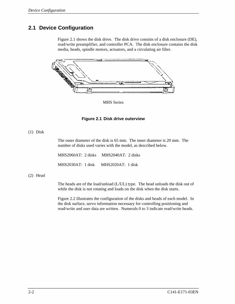
Figure 2.1 shows the disk drive. The disk drive consists of a disk enclosure (DE),read/write preamplifier, and controller PCA. The disk enclosure contains the diskmedia, heads, spindle motors, actuators, and a circulating air filter.
MHS Series
Figure 2.1 Disk drive outerview
(1) Disk
The outer diameter of the disk is 65 mm. The inner diameter is 20 mm. Thenumber of disks used varies with the model, as described below.
MHS2060AT: 2 disks MHS2040AT: 2 disks
MHS2030AT: 1 disk MHS2020AT: 1 disk
(2) Head
The heads are of the load/unload (L/UL) type. The head unloads the disk out ofwhile the disk is not rotating and loads on the disk when the disk starts.
Figure 2.2 illustrates the configuration of the disks and heads of each model. Inthe disk surface, servo information necessary for controlling positioning andread/write and user data are written. Numerals 0 to 3 indicate read/write heads.

2.1 Device Configuration
C141-E171-03EN 2-3
MHS2060AT
3
1
2
0
Head
Head
MHS2030ATMHS2020AT
1
0
MHS2040AT
1
2
0
3Head
Head 0 to Head 2 is mountedor Head 1 to Head 3 is mountedor Head 0 to Head 3 is mounted
Figure 2.2 Configuration of disk media heads
(3) Spindle motor
The disks are rotated by a direct drive Hall-less DC motor.
(4) Actuator
The actuator uses a revolving voice coil motor (VCM) structure which consumeslow power and generates very little heat. The head assembly at the edge of theactuator arm is controlled and positioned by feedback of the servo informationread by the read/write head. If the power is not on or if the spindle motor isstopped, the head assembly stays on the ramp out of the disk and is fixed by amechanical lock.
(5) Air circulation system
The disk enclosure (DE) is sealed to prevent dust and dirt from entering. The diskenclosure features a closed loop air circulation system that relies on the blowereffect of the rotating disk. This system continuously circulates the air through thecirculation filter to maintain the cleanliness of the air within the disk enclosure.
(6) Read/write circuit
The read/write circuit uses a LSI chip for the read/write preamplifier. It improvesdata reliability by preventing errors caused by external noise.
(7) Controller circuit
The controller circuit consists of an LSI chip to improve reliability. The high-speed microprocessor unit (MPU) achieves a high-performance AT controller.
Device Configuration
2-4 C141-E171-03EN
2.2 System Configuration
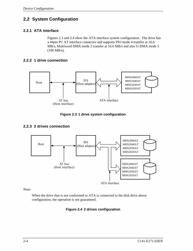
2.2.1 ATA interface
Figures 2.3 and 2.4 show the ATA interface system configuration. The drive hasa 44pin PC AT interface connector and supports PIO mode 4 transfer at 16.6MB/s, Multiword DMA mode 2 transfer at 16.6 MB/s and also U-DMA mode 5(100 MB/s).
2.2.2 1 drive connection
MHC2032ATMHC2040AT
Figure 2.3 1 drive system configuration
2.2.3 2 drives connection
MHC2032ATMHC2040AT
MHC2032ATMHC2040AT
(Host adaptor)
Note:
When the drive that is not conformed to ATA is connected to the disk drive aboveconfiguration, the operation is not guaranteed.
Figure 2.4 2 drives configuration
MHG2102ATMHH2064ATMHH2032AT
MHS2060ATMHS2040ATMHS2030ATMHS2020AT
MHS2060ATMHS2040ATMHS2030ATMHS2020AT
MHS2060ATMHS2040ATMHS2030ATMHS2020AT

2.2 System Configuration
C141-E171-03EN 2-5
IMPORTANT
HA (host adaptor) consists of address decoder, driver, and receiver.ATA is an abbreviation of “AT attachment”. The disk drive isconformed to the ATA-6 interface.At high speed data transfer (PIO mode 4 or DMA mode 2 U-DMAmode 5), occurrence of ringing or crosstalk of the signal lines (ATbus) between the HA and the disk drive may be a great cause of theobstruction of system reliability. Thus, it is necessary that thecapacitance of the signal lines including the HA and cable does notexceed the ATA-6 standard, and the cable length between the HAand the disk drive should be as short as possible.No need to push the top cover of the disk drive. If the over-powerworked, the cover could be contacted with the spindle motor. Thus,that could be made it the cause of failure.

This page is intentionally left blank.

C141-E171-03EN 3-1
CHAPTER 3 Installation Conditions
3.1 Dimensions
3.2 Mounting
3.3 Cable Connections
3.4 Jumper Settings
This chapter gives the external dimensions, installation conditions, surfacetemperature conditions, cable connections, and switch settings of the hard diskdrives.
For information about handling this hard disk drive and the system installationprocedure, refer to the following Integration Guide.C141-E144

Installation Conditions
3-2 C141-E171-03EN
3.1 Dimensions
Figure 3.1 illustrates the dimensions of the disk drive and positions of themounting screw holes. All dimensions are in mm.
Figure 3.1 Dimensions
3.2 Mounting
C141-E171-03EN 3-3
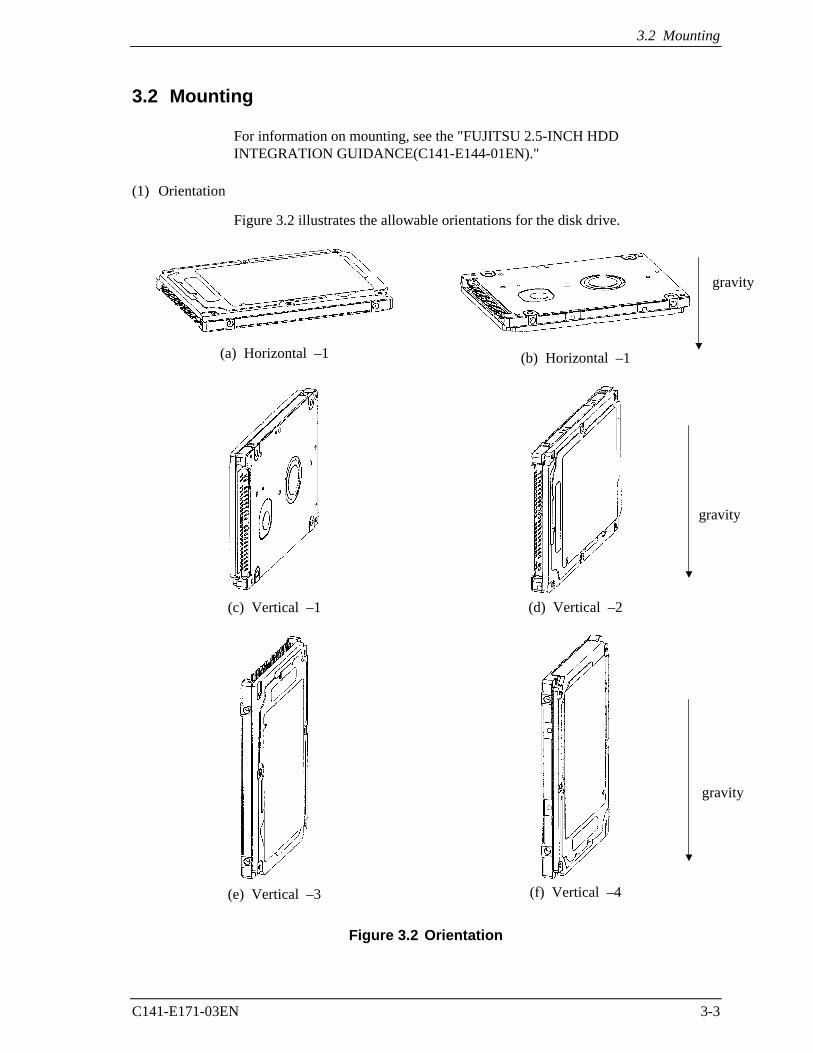
3.2 Mounting
For information on mounting, see the "FUJITSU 2.5-INCH HDDINTEGRATION GUIDANCE(C141-E144-01EN)."
(1) Orientation
Figure 3.2 illustrates the allowable orientations for the disk drive.
(a) Horizontal –1 (b) Horizontal –1
(c) Vertical –1 (d) Vertical –2
(e) Vertical –3 (f) Vertical –4
Figure 3.2 Orientation
gravity
gravity
gravity

Installation Conditions
3-4 C141-E171-03EN
(2) Frame
The MR head bias of the HDD disk enclosure (DE) is zero. The mounting frameis connected to SG.
IMPORTANT
Use M3 screw for the mounting screw and the screw length shouldsatisfy the specification in Figure 3.3.The tightening torque must be 0.49N·m(5kgf·cm).When attaching the HDD to the system frame, do not allow thesystem frame to touch parts (cover and base) other than parts towhich the HDD is attached.
(3) Limitation of mounting
Note) These dimensions are recommended values; if it is not possible tosatisfy them, contact us.
Figure 3.3 Mounting frame structure
ScrewScrew
Details of B
Details of A
3.0 or less3.0 or less
Frame of systemcabinetFrame of system
cabinet
BPCAA
2
2.52.5
2.52.5DE
Side surfacemountingBottom surface mounting

3.2 Mounting
C141-E171-03EN 3-5
IMPORTANT
Because of breather hole mounted to the HDD, do not allow this toclose during mounting.Locating of breather hole is shown as Figure 3.4.For breather hole of Figure 3.4, at least, do not allow its aroundφ2.4 to block.
Figure 3.4 Location of breather

Installation Conditions
3-6 C141-E171-03EN
(4) Ambient temperature
The temperature conditions for a disk drive mounted in a cabinet refer to theambient temperature at a point 3 cm from the disk drive. The ambienttemperature must satisfy the temperature conditions described in Section 1.4, andthe airflow must be considered to prevent the DE surface temperature fromexceeding 60°C.
Provide air circulation in the cabinet such that the PCA side, in particular,receives sufficient cooling. To check the cooling efficiency, measure the surfacetemperatures of the DE. Regardless of the ambient temperature, this surfacetemperature must meet the standards listed in Table 3.1. Figure 3.5 shows thetemperature measurement point.
Figure 3.5 Surface temperature measurement points
Table 3.1 Surface temperature measurement points and standard values
No. Measurement point Temperature
1 DE cover 60°C max
1
•

3.2 Mounting
C141-E171-03EN 3-7
(5) Service area
Figure 3.6 shows how the drive must be accessed (service areas) during and afterinstallation.
Figure 3.6 Service area
Data corruption: Avoid mounting the disk drive near strongmagnetic sources such as loud speakers. Ensure that the disk driveis not affected by external magnetic fields.Damage: Do not press the cover of the disk drive. Pressing it toohard, the cover and the spindle motor contact, which may causedamage to the disk drive.Static: When handling the device, disconnect the body ground(500 kΩ or greater). Do not touch the printed circuit board, buthold it by the edges.
(6) Handling cautions
Please keep the following cautions, and handle the HDD under the safetyenvironment.
Mounting screw hole
Mounting screw hole
Cable connection

Installation Conditions
3-8 C141-E171-03EN
- General notes
Figure 3.7 Handling cautions
- Installation
(1) Please use the driver of a low impact when you use an electric driver.HDD is occasionally damaged by the impact of the driver.
(2) Please observe the tightening torque of the screw strictly.M3 ······· 0.49N·m(5kgf·cm).
- Recommended equipments
Contents Model Maker
Wrist strap JX-1200-3056-8 SUMITOMO 3MESD
ESD mat SKY-8A (Color Seiden Mat) Achilles
Shock Low shock driver SS-6500 HIOS
Place the shock absorbing mat on theoperation table, and place ESD mat on it.
Use the Wrist strap.
Do not hit HDD each other. Do not stack when carrying.
Do not place HDD verticallyto avoid falling down. Do not drop.
Shock absorbing mat
ESD mat
Wrist strap

3.3 Cable Connections
C141-E171-03EN 3-9
3.3 Cable Connections
3.3.1 Device connector
The disk drive has the connectors and terminals listed below for connectingexternal devices. Figure 3.8 shows the locations of these connectors andterminals.
Figure 3.8 Connector locations
Connector,setting pins
PCA

Installation Conditions
3-10 C141-E171-03EN
3.3.2 Cable connector specifications
Table 3.2 lists the recommended specifications for the cable connectors.
Table 3.2 Cable connector specifications
Name Model Manufacturer
ATA interface and powersupply cable (44-pin type)
Cable socket(44-pin type)
89361-144 FCI
IMPORTANT
For the host interface cable, use a ribbon cable. A twisted cable ora cable with wires that have become separated from the ribbon maycause crosstalk between signal lines. This is because the interfaceis designed for ribbon cables and not for cables carrying differentialsignals.
3.3.3 Device connection
Figure 3.9 shows how to connect the devices.
Host system
DCPower supply
Disk Drive #0
Disk Drive #1
Inte
rfac
e
Interface
Power supply cable
Figure 3.9 Cable connections

3.4 Jumper Settings
C141-E171-03EN 3-11
3.3.4 Power supply connector (CN1)
Figure 3.10 shows the pin assignment of the power supply connector (CN1).
Figure 3.10 Power supply connector pins (CN1)
3.4 Jumper Settings
3.4.1 Location of setting jumpers
Figure 3.11 shows the location of the jumpers to select drive configuration andfunctions.
Figure 3.11 Jumper location

Installation Conditions
3-12 C141-E171-03EN
3.4.2 Factory default setting
Figure 3.12 shows the default setting position at the factory.
Figure 3.12 Factory default setting
3.4.3 Master drive-slave drive setting
Master drive (disk drive #0) or slave drive (disk drive #1) is selected.
(b) Slave drive(a) Master drive
Open
Open
ShortOpen
A1 C
BD2 BD2
AC1
Figure 3.13 Jumper setting of master or slave drive
Note:
Pins A and C should be open.
Open

3.4 Jumper Settings
C141-E171-03EN 3-13
3.4.4 CSEL setting
Figure 3.14 shows the cable select (CSEL) setting.
Short
Open
BD2
AC1
Note:
The CSEL setting is not depended on setting between pins Band D.
Figure 3.14 CSEL setting
Figure 3.15 and 3.16 show examples of cable selection using unique interfacecables.
By connecting the CSEL of the master drive to the CSEL Line (conducer) of thecable and connecting it to ground further, the CSEL is set to low level. The driveis identified as a master drive. At this time, the CSEL of the slave drive does nothave a conductor. Thus, since the slave drive is not connected to the CSELconductor, the CSEL is set to high level. The drive is identified as a slave drive.
Figure 3.15 Example (1) of Cable Select
drive drive

Installation Conditions
3-14 C141-E171-03EN
Figure 3.16 Example (2) of Cable Select
3.4.5 Power Up in Standby setting
When pin C is grounded, the drive does not spin up at power on.
drive drive
C141-E171-03EN 4-1
CHAPTER 4 Theory of Device Operation
4.1 Outline
4.2 Subassemblies
4.3 Circuit Configuration
4.4 Power-on Sequence
4.5 Self-calibration
4.6 Read/write Circuit
4.7 Servo Control
This chapter explains basic design concepts of the disk drive. Also, this chapterexplains subassemblies of the disk drive, each sequence, servo control, andelectrical circuit blocks.

Theory of Device Operation
4-2 C141-E171-03EN
4.1 Outline
This chapter consists of two parts. First part (Section 4.2) explains mechanicalassemblies of the disk drive. Second part (Sections 4.3 through 4.7) explains aservo information recorded in the disk drive and drive control method.
4.2 Subassemblies
The disk drive consists of a disk enclosure (DE) and printed circuit assembly(PCA).
The DE contains all movable parts in the disk drive, including the disk, spindle,actuator, read/write head, and air filter. For details, see Subsections 4.2.1 to 4.2.5.
The PCA contains the control circuits for the disk drive. The disk drive has onePCA. For details, see Sections 4.3.
4.2.1 Disk
The DE contains disks with an outer diameter of 65 mm and an inner diameter of20 mm. The MHS2060AT and MHS2040AT have two disks and MHS2030ATand MHS2020AT have one disk.
Servo data is recorded on each cylinder (total 120). Servo data written at factoryis read out by the read head. For servo data, see Section 4.7.
4.2.2 Head
Figure 4.1 shows the head structures. MHS2060AT has 4 heads andMHS2040AT has 3 heads and MHS2030AT and MHS2020AT have 2 heads.

4.2 Subassemblies
C141-E171-03EN 4-3
MHS2060AT
3
1
2
0
Head
Head
MHS2030ATMHS2020AT
1
0
MHS2040AT
1
2
0
3Head
Head 0 to Head 2 is mountedor Head 1 to Head 3 is mountedor Head 0 to Head 3 is mounted
Figure 4.1 Head structure
4.2.3 Spindle
The spindle consists of a disk stack assembly and spindle motor. The disk stackassembly is activated by the direct drive sensor-less DC spindle motor, which hasa speed of 4,200 rpm ±1%. The spindle is controlled with detecting a PHASEsignal generated by counter electromotive voltage of the spindle motor at starting.
4.2.4 Actuator
The actuator consists of a voice coil motor (VCM) and a head carriage. TheVCM moves the head carriage along the inner or outer edge of the disk. The headcarriage position is controlled by feeding back the difference of the target positionthat is detected and reproduced from the servo information read by the read/writehead.
4.2.5 Air filter
There are two types of air filters: a breather filter and a circulation filter.
The breather filter makes an air in and out of the DE to prevent unnecessarypressure around the spindle when the disk starts or stops rotating. When diskdrives are transported under conditions where the air pressure changes a lot,filtered air is circulated in the DE.
The circulation filter cleans out dust and dirt from inside the DE. The disk drivecycles air continuously through the circulation filter through an enclosed loop aircycle system operated by a blower on the rotating disk.

Theory of Device Operation
4-4 C141-E171-03EN
4.3 Circuit Configuration
Figure 4.2 shows the power supply configuration of the disk drive, and Figure 4.3shows the disk drive circuit configuration.
(1) Read/write circuit
The read/write circuit consists of two LSIs; read/write preamplifier (PreAMP) andread channel (RDC).
The PreAMP consists of the write current switch circuit, that flows the writecurrent to the head coil, and the voltage amplifier circuit, that amplitudes the readoutput from the head.
The RDC is the read demodulation circuit using the Modified Extended PartialResponse (MEEPR), and contains the Viterbi detector, programmable filter,adaptable transversal filter, times base generator, data separator circuits, 48/50RLL (Limited) encoder Run Length and servo demodulation circuit.
(2) Servo circuit
The position and speed of the voice coil motor are controlled by 2 closed-loopservo using the servo information recorded on the data surface. The servoinformation is an analog signal converted to digital for processing by a MPU andthen reconverted to an analog signal for control of the voice coil motor.
The MPU precisely sets each head on the track according on the servoinformation on the media surface.
(3) Spindle motor driver circuit
The circuit measures the interval of a PHASE signal generated by counter-electromotive voltage of a motor and controls the motor speed comparing targetspeed.
(4) Controller circuit
Major functions are listed below.
• Data buffer (2 MB) management
• ATA interface control and data transfer control
• Sector format control
• Defect management
• ECC control
• Error recovery and self-diagnosis

4.3 Circuit Configuration
C141-E171-03EN 4-5
5.0V
3.3V - 3.0VS-DRAM SVC HDIC F-ROM
MCU&
HDC
RDC
2.0V
1.8-Vgenerator
circuit
Figure 4.2 Power Supply Configuration

Theory of Device Operation
4-6 C141-E171-03EN
Figure 4.3 Circuit Configuration

4.4 Power-on Sequence
C141-E171-03EN 4-7
4.4 Power-on Sequence
Figure 4.4 describes the operation sequence of the disk drive at power-on. Theoutline is described below.
a) After the power is turned on, the disk drive executes the MPU bus test,internal register read/write test, and work RAM read/write test. When theself-diagnosis terminates successfully, the disk drive starts the spindle motor.
b) The disk drive executes self-diagnosis (data buffer read/write test) afterenabling response to the ATA bus.
c) After confirming that the spindle motor has reached rated speed, the headassembly is loaded on the disk.
d) The disk drive positions the heads onto the SA area and reads out the systeminformation.
e) The disk drive sets up a requirement for execution of self-seek-calibration.This collects data for VCM torque and mechanical external forces applied tothe actuator, and updates the calibrating value.
f) The drive becomes ready. The host can issue commands.

Theory of Device Operation
4-8 C141-E171-03EN
Figure 4.4 Power-on operation sequence
4.5 Self-calibration
The disk drive occasionally performs self-calibration in order to sense andcalibrate mechanical external forces on the actuator, and VCM torque. Thisenables precise seek and read/write operations.
4.5.1 Self-calibration contents
(1) Sensing and compensating for external forces
The actuator suffers from torque due to the FPC forces and winds accompanyingdisk revolution. The torque vary with the disk drive and the cylinder where thehead is positioned. To execute stable fast seek operations, external forces areoccasionally sensed.
The firmware of the drive measures and stores the force (value of the actuatormotor drive current) that balances the torque for stopping head stably. Thisincludes the current offset in the power amplifier circuit and DAC system.
Start
Self-diagnosis 1- MPU bus test- Internal register write/read test- Work RAM write/read test
Power-on
a)
The spindle motor starts.
Self-diagnosis 2- Data buffer write/read test
b)
Confirming spindle motorspeed
c)
Load the head assembly Drive ready state(command waiting state)
f)
Execute self-calibratione)
Initial on-track and readout of system information
d)
End

4.5 Self-calibration
C141-E171-03EN 4-9
The forces are compensated by adding the measured value to the specified currentvalue to the power amplifier. This makes the stable servo control.
To compensate torque varying by the cylinder, the disk is divided into 16 areasfrom the innermost to the outermost circumference and the compensating value ismeasured at the measuring cylinder on each area at factory calibration. Themeasured values are stored in the SA cylinder. In the self-calibration, thecompensating value is updated using the value in the SA cylinder.
(2) Compensating open loop gain
Torque constant value of the VCM has a dispersion for each drive, and variesdepending on the cylinder that the head is positioned. To realize the high speedseek operation, the value that compensates torque constant value change and loopgain change of the whole servo system due to temperature change is measuredand stored.
For sensing, the firmware mixes the disturbance signal to the position signal at thestate that the head is positioned to any cylinder. The firmware calculates the loopgain from the position signal and stores the compensation value against to thetarget gain as ratio.
For compensating, the direction current value to the power amplifier is multipliedby the compensation value. By this compensation, loop gain becomes constantvalue and the stable servo control is realized.
To compensate torque constant value change depending on cylinder, wholecylinders from most inner to most outer cylinder are divided into 14 partitions atcalibration in the factory, and the compensation data is measured forrepresentative cylinder of each partition. This measured value is stored in the SAarea. The compensation value at self-calibration is calculated using the value inthe SA area.
4.5.2 Execution timing of self-calibration
Self-calibration is performed once when power is turned on. After that, the diskdrive does not perform self-calibration until it detects an error.
That is, self-calibration is performed each time one of the following events occur:
• When it passes from the power on for ten seconds and the disk drive shifts toActive Idle mode.
• The number of retries to write or seek data reaches the specified value.
• The error rate of data reading, writing, or seeking becomes lower than thespecified value.

Theory of Device Operation
4-10 C141-E171-03EN
4.5.3 Command processing during self-calibration
This enables the host to execute the command without waiting for a long time,even when the disk drive is performing self-calibration. The command executionwait time is about maximum 72 ms.
When the error rate of data reading, writing, or seeking becomes lower than thespecified value, self-calibration is performed to maintain disk drive stability.
If the disk drive receives a command execution request from the host whileperforming self-calibration, it stops the self-calibration and starts to execute thecommand. In other words, if a disk read or write service is necessary, the diskdrive positions the head to the track requested by the host, reads or writes data,and then restarts calibration after 10 seconds.
If the error rate recovers to a value exceeding the specified value, self-calibrationis not performed.
4.6 Read/write Circuit
The read/write circuit consists of the read/write preamplifier (HDIC), the writecircuit, the read circuit, and the time base generator in the read channel (RDC).Figure 4.4 is a block diagram of the read/write circuit.
4.6.1 Read/write preamplifier (HDIC)
HDIC equips a read preamplifier and a write current switch, that sets the biascurrent to the MR device and the current in writing. Each channel is connected toeach data head, and HDIC switches channel by serial I/O. In the event of anyabnormalities, including a head short-circuit or head open circuit, the write unsafesignal is generated so that abnormal write does not occur.
4.6.2 Write circuit
The write data is output from the hard disk controller (HDC) with the NRZ dataformat, and sent to the encoder circuit in the RDC. The NRZ write data isconverted from 48-bit data to 50-bit data by the encoder circuit then sent to theHDIC, and the data is written onto the media.
(1) 48/50 RLL MEEPRML
This device converts data using the 48/50 RLL (Run Length Limited) algorithm.
(2) Write precompensation
Write precompensation compensates, during a write process, for write non-linearity generated at reading.

4.6 Read/write Circuit
C141-E171-03EN 4-11
Figure 4.5 Read/write circuit block diagram
HDIC
WDX/WDY RDX/RDY
WritePreCompen-sation
Serial I/O
Registers
DigitalPLL
FlashDigitizer
MEEPRViterbiDetect
16/17ENDEC
ServoPulseDetector
ProgrammableFilter
AGCAmplifier
RDCSD SC SE
PositionA/B/C/D(to reg)
WTGATE REFCLK RDGATE DATA[7:0]
RWCLK SRV_OUT[1:0]SRV_CLK

Theory of Device Operation
4-12 C141-E171-03EN
4.6.3 Read circuit
The head read signal from the PreAMP is regulated by the automatic gain control(AGC) circuit. Then the output is converted into the sampled read data pulse bythe programmable filter circuit and the flash digitizer circuit. This clock signal isconverted into the NRZ data by the ENDEC circuit based on the read datamaximum-likelihood-detected by the Viterbi detection circuit, then is sent to theHDC.
(1) AGC circuit
The AGC circuit automatically regulates the output amplitude to a constant valueeven when the input amplitude level fluctuates. The AGC amplifier output ismaintained at a constant level even when the head output fluctuates due to thehead characteristics or outer/inner head positions.
(2) Programmable filter circuit
The programmable filter circuit has a low-pass filter function that eliminatesunnecessary high frequency noise component and a high frequency boost-upfunction that equalizes the waveform of the read signal.
Cut-off frequency of the low-pass filter and boost-up gain are controlled from theregister in read channel by an instruction of the serial data signal from MPU(M5). The MPU optimizes the cut-off frequency and boost-up gain according tothe transfer frequency of each zone.
Figure 4.6 shows the frequency characteristic sample of the programmable filter.
Figure 4.6 Frequency characteristic of programmable filter
-3 dB

4.6 Read/write Circuit
C141-E171-03EN 4-13
(3) FIR circuit
This circuit is 10-tap sampled analog transversal filter circuit that equalizes thehead read signal to the Modified Extended Partial Response (MEEPR) waveform.
(4) A/D converter circuit
This circuit changes Sampled Read Data Pulse from the FIR circuit into DigitalRead Data.
(5) Viterbi detection circuit
The sample hold waveform output from the flash digitizer circuit is sent to theViterbi detection circuit. The Viterbi detection circuit demodulates dataaccording to the survivor path sequence.
(6) ENDEC
This circuit converts the 50-bit read data into the 48-bit NRZ data.
4.6.4 Digital PLL circuit
The drive uses constant density recording to increase total capacity. This isdifferent from the conventional method of recording data with a fixed datatransfer rate at all data area. In the constant density recording method, data areais divided into zones by radius and the data transfer rate is set so that therecording density of the inner cylinder of each zone is nearly constant. The drivedivides data area into 30 zones to set the data transfer rate.
The MPU transfers the data transfer rate setup data (SD/SC) to the RDC thatincludes the Digital PLL circuit to change the data transfer rate.

Theory of Device Operation
4-14 C141-E171-03EN
4.7 Servo Control
The actuator motor and the spindle motor are submitted to servo control. Theactuator motor is controlled for moving and positioning the head to the trackcontaining the desired data. To turn the disk at a constant velocity, the actuatormotor is controlled according to the servo data that is written on the data sidebeforehand.
4.7.1 Servo control circuit
Figure 4.7 is the block diagram of the servo control circuit. The followingdescribes the functions of the blocks:
Figure 4.7 Block diagram of servo control circuit
(1) Microprocessor unit (MPU)
The MPU uses DSP and executes startup of the spindle motor, movement to thereference cylinder, seek to the specified cylinder, and calibration operations.Main internal operation of the MPU are shown below.
Head
Spindlemotor
CSR
VCM
Position Sense
VCM current
CSR: Current Sense ResisterVCM: Voice Coil Motor
(1)MPU
(2)
Servoburstcapture
(3)
DAC
(4)SVC
PowerAmp
(5)
Spindlemotorcontrol
(6)
Driver
(7)
MPUcore

4.7 Servo Control
C141-E171-03EN 4-15
The major internal operations are listed below.
a. Spindle motor start
Starts the spindle motor and accelerates it to normal speed when power isapplied.
b. Move head to reference cylinder
Drives the VCM to position the head at the any cylinder in the data area. Thelogical initial cylinder is at the outermost circumference (cylinder 0).
c. Seek to specified cylinder
Drives the VCM to position the head to the specified cylinder.
d. Calibration
Senses and stores the thermal offset between heads and the mechanical forceson the actuator, and stores the calibration value.

Theory of Device Operation
4-16 C141-E171-03EN
(2) Servo burst capture circuit
The servo burst capture circuit reproduces signals (position signals) that indicatethe head position from the servo data on the data surface. From the servo area onthe data area surface, via the data head, the burst signal of SERVO A, SERVO B,SERVO C, and SERVO D is output as shown in Figure 4.9 in subsequent to theservo mark, gray code that indicates the cylinder position, and index information.The servo signals do A/D-convert by Fourier-demodulator in the servo burstcapture circuit. At that time the AGC circuit is in hold mode. The A/D converteddata is recognized by the MPU as position information with A-B and C-Dprocessed.
(3) D/A converter (DAC)
The control program calculates the specified data value (digital value) of theVCM drive current, and the value is converted from digital-to-analog so that ananalog output voltage is sent to the power amplifier.
(4) Power amplifier
The power amplifier feeds currents, corresponding to the DAC output signalvoltage to the VCM.
(5) Spindle motor control circuit
The spindle motor control circuit controls the sensor-less spindle motor. Aspindle driver IC with a built-in PLL(FLL) circuit that is on a hardware unitcontrols the sensor-less spindle motor.
(6) Driver circuit
The driver circuit is a power amplitude circuit that receives signals from thespindle motor control circuit and feeds currents to the spindle motor.
(7) VCM current sense resistor (CSR)
This resistor controls current at the power amplifier by converting the VCMcurrent into voltage and feeding back.

4.7 Servo Control
C141-E171-03EN 4-17
4.7.2 Data-surface servo format
Figure 4.8 describes the physical layout of the servo frame. The three areasindicated by (1) to (3) in Figure 4.8 are described below.
(1) Inner guard band
This area is located inside the user area, and the rotational speed of the VCM canbe controlled on this cylinder area for head moving.
(2) Data area
This area is used as the user data area SA area.
(3) Outer guard band
This area is located at outer position of the user data area, and the rotational speedof the spindle can be controlled on this cylinder area for head moving.

Theory of Device Operation
4-18 C141-E171-03EN
Figure 4.8 Physical sector servo configuration on disk surface
W/R Recovery Servo Mark Gray Code
W/R RecoveryServo MarkGray Code
W/R RecoveryServo MarkGray Code
Erase Servo A Erase Servo A
Servo B Erase Servo B Erase
Servo C Erase Servo C
Erase Servo D Erase
PAD
CYLn + 1 CYLn CYLn – 1 (n: even number) Diameter
direction
CircumferenceDirection
Erase: DC erase area
OGBData areaIGB
expand
Servo frame(140 servo frames per revolution)

4.7 Servo Control
C141-E171-03EN 4-19
4.7.3 Servo frame format
As the servo information, the IDD uses the two-phase servo generated from thegray code and servo A to D. This servo information is used for positioningoperation of radius direction and position detection of circumstance direction.
The servo frame consists of 6 blocks; write/read recovery, servo mark, gray code,servo A to D, and PAD. Figure 4.9 shows the servo frame format.
Figure 4.9 Servo frame format

Theory of Device Operation
4-20 C141-E171-03EN
(1) Write/read recovery
This area is used to absorb the write/read transient and to stabilize the AGC.
(2) Servo mark
This area generates a timing for demodulating the gray code and position-demodulating the servo A to D by detecting the servo mark.
(3) Gray code (including index bit)
This area is used as cylinder address. The data in this area is converted into thebinary data by the gray code demodulation circuit
(4) Servo A, servo B, servo C, servo D
This area is used as position signals between tracks and the IDD control at on-track so that servo A level equals to servo B level.
(5) PAD
This area is used as a gap between servo and data.
4.7.4 Actuator motor control
The voice coil motor (VCM) is controlled by feeding back the servo data recordedon the data surface. The MPU fetches the position sense data on the servo frameat a constant interval of sampling time, executes calculation, and updates theVCM drive current.
The servo control of the actuator includes the operation to move the head to thereference cylinder, the seek operation to move the head to the target cylinder toread or write data, and the track-following operation to position the head onto thetarget track.
(1) Operation to move the head to the reference cylinder
The MPU moves the head to the reference cylinder when the power is turned.The reference cylinder is in the data area.
When power is applied the heads are moved from the inner circumference shuntzone to the normal servo data zone in the following sequence:
a) Micro current is fed to the VCM to press the head against the outercircumference.
b) The head is loaded on the disk.
c) When the servo mark is detected the head is moved slowly toward the innercircumference at a constant speed.

4.7 Servo Control
C141-E171-03EN 4-21
d) If the head is stopped at the reference cylinder from there. Track followingcontrol starts.
(2) Seek operation
Upon a data read/write request from the host, the MPU confirms the necessity ofaccess to the disk. If a read/write instruction is issued, the MPU seeks the desiredtrack.
The MPU feeds the VCM current via the D/A converter and power amplifier tomove the head. The MPU calculates the difference (speed error) between thespecified target position and the current position for each sampling timing duringhead moving. The MPU then feeds the VCM drive current by setting thecalculated result into the D/A converter. The calculation is digitally executed bythe firmware. When the head arrives at the target cylinder, the track is followed.
(3) Track following operation
Except during head movement to the reference cylinder and seek operation underthe spindle rotates in steady speed, the MPU does track following control. Toposition the head at the center of a track, the DSP drives the VCM by feedingmicro current. For each sampling time, the VCM drive current is determined byfiltering the position difference between the target position and the positionclarified by the detected position sense data. The filtering includes servocompensation. These are digitally controlled by the firmware.
4.7.5 Spindle motor control
Hall-less three-phase twelve-pole motor is used for the spindle motor, and the 3-phase full/half-wave analog current control circuit is used as the spindle motordriver (called SVC hereafter). The firmware operates on the MPU manufacturedby Fujitsu. The spindle motor is controlled by sending several signals from theMPU to the SVC. There are three modes for the spindle control; start mode,acceleration mode, and stable rotation mode.
(1) Start mode
When power is supplied, the spindle motor is started in the following sequence:
a) After the power is turned on, the MPU sends a signal to the SVC to chargethe charge pump capacitor of the SVC. The charged amount defines thecurrent that flows in the spindle motor.
b) When the charge pump capacitor is charged enough, the MPU sets the SVCto the motor start mode. Then, a current (approx. 0.3 A) flows into thespindle motor.
c) A phase switching signal is generated and the phase of the current flowed inthe motor is changed in the order of (V-phase to U-phase), (W-phase to U-phase), (W-phase to V-phase), (U-phase to V-phase), (U-phase to W-phase),and (V-phase to W-phase) (after that, repeating this order).

Theory of Device Operation
4-22 C141-E171-03EN
d) During phase switching, the spindle motor starts rotating in low speed, andgenerates a counter electromotive force. The SVC detects this counterelectromotive force and reports to the MPU using a PHASE signal for speeddetection.
e) The MPU is waiting for a PHASE signal. When no phase signal is sent for aspecific period, the MPU resets the SVC and starts from the beginning.When a PHASE signal is sent, the SVC enters the acceleration mode.
(2) Acceleration mode
In this mode, the MPU stops to send the phase switching signal to the SVC. TheSVC starts a phase switching by itself based on the counter electromotive force.Then, rotation of the spindle motor accelerates. The MPU calculates a rotationalspeed of the spindle motor based on the PHASE signal from the SVC, and waitstill the rotational speed reaches 4,200 rpm. When the rotational speed reaches4,200 rpm, the SVC enters the stable rotation mode.
(3) Stable rotation mode
The SVC calculates a time for one revolution of the spindle motor based on thePHASE signal. The MPU takes a difference between the current time and a timefor one revolution at 4,200 rpm that the MPU already recognized. Then, the MPUkeeps the rotational speed to 4,200 rpm by charging or discharging the chargepump for the different time. For example, when the actual rotational speed is4,000 rpm, the time for one revolution is 15.000 ms. And the time for onerevolution at 4,200 rpm is 14.286 ms. Therefore, the MPU charges the chargepump for 0.714 ms × k (k: constant value). This makes the flowed current intothe motor higher and the rotational speed up. When the actual rotational speed isfaster than 4,200 rpm, the MPU discharges the pump the other way. This control(charging/discharging) is performed every 1 revolution.

C141-E171-03EN 5-1
CHAPTER 5 Interface
5.1 Physical Interface
5.2 Logical Interface
5.3 Host Commands
5.4 Command Protocol
5.5 Ultra DMA Feature Set
5.6 Timing
This chapter gives details about the interface, and the interface commands andtimings.

Interface
5-2 C141-E171-03EN
5.1 Physical Interface
5.1.1 Interface signals
Figure 5.1 shows the interface signals.
Figure 5.1 Interface signals
DATA 0-15: DATA BUS
DMACK-: DMA ACKNOWLEDGE
PDIAG-: PASSED DIAGNOSTICSCBLID-: CABLE TYPE IDENTIFIERDASP-: DEVICE ACTIVE/SLAVE PRESENT
DMARQ: DMA REQUESTINTRO: INTERRUPT REQUEST
DIOW-: I/O WRITESTOP: STOP DURING ULTRA DMA DATA BURSTS
DA 0-2: DEVICE ADDRESSCS0-: CHIP SELECT 0CS1-: CHIP SELECT 1
RESET-: RESETCSEL: CABLE SELECT
MSTR: MasterENCSEL: ENABLE CSEL
GND: GROUND
DIOR-:I/O READHDMARDY:DMA READY DURING ULTRA DMA DATA IN BURSTSHSTROBE:DATA STROBE DURING ULTRA DMA DATA OUT BURST
+5V DC: +5 volt
Host
IORDY:I/O READYDDMARDY:DMA READY DURING ULTRA DMA DATA OUT BURSTSDSTROBE: DATA STROBE DURING ULTRA DMA DATA IN BURSTS
IDD

5.1 Physical Interface
C141-E171-03EN 5-3
5.1.2 Signal assignment on the connector
Table 5.1 shows the signal assignment on the interface connector.
Table 5.1 Signal assignment on the interface connector
Pin No. Signal Pin No. Signal
A
C
E
1
3
5
7
9
11
13
15
17
19
21
23
25
27
29
31
33
35
37
39
41
43
MSTR
PUS-
(KEY)
RESET–
DATA7
DATA6
DATA5
DATA4
DATA3
DATA2
DATA1
DATA0
GND
DMARQ
DIOW-, STOP
DIOR-, HDMRDY,HSTROBE
IORDY, DDMARDY,DSTROBE
DMACK–
INTRQ
DA1
DA0
CS0–
DASP–
+5 VDC
GND
B
D
F
2
4
6
8
10
12
14
16
18
20
22
24
26
28
30
32
34
36
38
40
42
44
MSTR/ENCSEL
ENCSEL
(KEY)
GND
DATA8
DATA9
DATA10
DATA11
DATA12
DATA13
DATA14
DATA15
(KEY)
GND
GND
GND
CSEL
GND
reserved (IOCS16-)
PDIAG–, CBLID–
DA2
CS1–
GND
+5 VDC
unused

Interface
5-4 C141-E171-03EN
[signal] [I/O] [Description]
ENCSEL I This signal is used to set master/slave using the CSEL signal (pin 28).
Pins B and D Open: Sets master/slave using the CSEL signalis disabled.
Short: Sets master/slave using the CSEL signalis enabled.
MSTR- I MSTR, I, Master/slave settingPin A, B, C, D open: Master settingPin A, B Short: Slave setting
PUS- I When pin C is grounded, the drive does not spin up at power on.
RESET- I Reset signal from the host. This signal is low active and isasserted for a minimum of 25 µs during power on.
DATA 0-15 I/O Sixteen-bit bi-directional data bus between the host and thedevice. These signals are used for data transfer
DIOW- I Signal asserted by the host to write to the device register or dataport.
STOP I DIOW- must be negated by the host before starting the UltraDMA transfer. The STOP signal must be negated by the hostbefore data is transferred during the Ultra DMA transfer. Duringdata transfer in Ultra DMA mode, the assertion of the STOPsignal asserted by the host later indicates that the transfer has beensuspended.
DIOR- I Read strobe signal from the host to read the device register or dataport
HDMARDY- I Flow control signal for Ultra DMA data In transfer (READ DMAcommand). This signal is asserted by the host to inform thedevice that the host is ready to receive the Ultra DMA data Intransfer. The host can negate the HDMARDY- signal to suspendthe Ultra DMA data In transfer.
HSTROBE I Data Out Strobe signal from the host during Ultra DMA data Outtransfer (WRITE DMA command). Both the rising and fallingedges of the HSTROBE signal latch data from Data 15-0 into thedevice. The host can suspend the inversion of the HSTROBEsignal to suspend the Ultra DMA data Out transfer.
INTRQ O Interrupt signal to the host.
This signal is negated in the following cases:
− assertion of RESET- signal
− Reset by SRST of the Device Control register
− Write to the command register by the host
− Read of the status register by the host
− Completion of sector data transfer
(without reading the Status register)
The signal output line has a high impedance when no devices areselected or interruption is disabled.

5.1 Physical Interface
C141-E171-03EN 5-5
[signal] [I/O] [Description]
CS0- I Chip select signal decoded from the host address bus. This signalis used by the host to select the command block registers.
CS1- I Chip select signal decoded from the host address bus. This signalis used by the host to select the control block registers.
DA 0-2 I Binary decoded address signals asserted by the host to access taskfile registers.
KEY - Key pin for prevention of erroneous connector insertion
PDIAG- I/O This signal is an input mode for the master device and an outputmode for the slave device in a daisy chain configuration. Thissignal indicates that the slave device has been completed selfdiagnostics.
This signal is pulled up to +5 V through 10 kΩ resistor at each device.
CBLID- I/O This signal is used to detect the type of cable installed in thesystem.
This signal is pulled up to +5 V through 10 kΩ resistor at each device.
DASP- I/O This is a time-multiplexed signal that indicates that the device isactive and a slave device is present.
This signal is pulled up to +5 V through 10 kΩ resistor at each device.
IORDY O This signal requests the host system to delay the transfer cyclewhen the device is not ready to respond to a data transfer requestfrom the host system.
DDMARDY- O Flow control signal for Ultra DMA data Out transfer (WRITEDMA command). This signal is asserted by the device to informthe host that the device is ready to receive the Ultra DMA dataOut transfer. The device can negate the DDMARDY- signal tosuspend the Ultra DMA data Out transfer.
DSTROBE O Data In Strobe signal from the device during Ultra DMA data Intransfer. Both the rising and falling edges of the DSTROBEsignal latch data from Data 15-0 into the host. The device cansuspend the inversion of the DSTROBE signal to suspend theUltra DMA data In transfer.
CSEL I This signal to configure the device as a master or a slave device.
− When CSEL signal is grounded, the IDD is a master device.
− When CSEL signal is open, the IDD is a slave device.
This signal is pulled up with 240 kΩ resistor at each device.
DMACK- I The host system asserts this signal as a response that the hostsystem receive data or to indicate that data is valid.

Interface
5-6 C141-E171-03EN
[signal] [I/O] [Description]
DMARQ O This signal is used for DMA transfer between the host system andthe device. The device asserts this signal when the devicecompletes the preparation of DMA data transfer to the hostsystem (at reading) or from the host system (at writing).
The direction of data transfer is controlled by the DIOR andDIOW signals. This signal hand shakes with the DMACK-signal.In other words, the device negates the DMARQ signal after thehost system asserts the DMACK signal. When there is other datato be transferred, the device asserts the DMARQ signal again.
When the DMA data transfer is performed, IOCS16-, CS0- andCS1- signals are not asserted. The DMA data transfer is a 16-bitdata transfer.
+5 VDC I +5 VDC power supplying to the device.
GND - Grounded signal at each signal wire.
Note:
“I” indicates input signal from the host to the device.
“O” indicates output signal from the device to the host.
“I/O” indicates common output or bi-directional signal between the hostand the device.
5.2 Logical Interface
The device can operate for command execution in either address-specified mode;cylinder-head-sector (CHS) or Logical block address (LBA) mode. TheIDENTIFY DEVICE information indicates whether the device supports the LBAmode. When the host system specifies the LBA mode by setting bit 6 in theDevice/Head register to 1, HS3 to HS0 bits of the Device/Head register indicatesthe head No. under the LBA mode, and all bits of the Cylinder High, CylinderLow, and Sector Number registers are LBA bits.
The sector No. under the LBA mode proceeds in the ascending order with thestart point of LBA0 (defined as follows).
LBA0 = [Cylinder 0, Head 0, Sector 1]
Even if the host system changes the assignment of the CHS mode by theINITIALIZE DEVICE PARAMETER command, the sector LBA address is notchanged.
LBA = [((Cylinder No.) × (Number of head) + (Head No.)) × (Number ofsector/track)] + (Sector No.) − 1

5.2 Logical Interface
C141-E171-03EN 5-7
5.2.1 I/O registers
Communication between the host system and the device is done through input-output (I/O) registers of the device.
These I/O registers can be selected by the coded signals, CS0-, CS1-, and DA0 toDA2 from the host system. Table 5.2. shows the coding address and the functionof I/O registers.
Table 5.2 I/O registers
I/O registers
Read operation Write operation
Command block registers
L H L L L Data Data X’1F0’
L H L L H Error Register Features X’1F1’
L H L H L Sector Count Sector Count X’1F2’
L H L H H Sector Number Sector Number X’1F3’
L H H L L Cylinder Low Cylinder Low X’1F4’
L H H L H Cylinder High Cylinder High X’1F5’
L H H H L Device/Head Device/Head X’1F6’
L H H H H Status Command X’1F7’
L L X X X (Invalid) (Invalid) —
Control block registers
H L H H L Alternate Status Device Control X’3F6’
H L H H H — — X’3F7’
Notes:
1. The Data register for read or write operation can be accessed by 16 bit databus (DATA0 to DATA15).
2. The registers for read or write operation other than the Data registers can beaccessed by 8 bit data bus (DATA0 to DATA7).
3. When reading the Drive Address register, bit 7 is high-impedance state.
4. H indicates signal level High and L indicates signal level Low.
There are two methods for specifying the LBA mode. One method is tospecify the LBA mode with 28-bit address information, and the other is tospecify it with 48-bit address information (command of EXT system). Ifthe LBA mode is specified with 28-bit address information, the
Host I/Oaddress
DA0DA1DA2CS1–CS0–

Interface
5-8 C141-E171-03EN
Device/Head, Cylinder High, Cylinder Low, Sector Number registersindicate LBA bits 27 to 24, bits 23 to 16, bits 15 to 8, and bits 7 to 0,respectively.
If the LBA mode is specified with 48-bit address information, the CylinderHigh, Cylinder Low, Sector Number registers are set twice. In the firsttime, the registers indicate LBA bits 47 to 40, bits 39 to 32, and bits 31 to24, respectively. In the second time, the registers indicate LBA bits 23 to16, bits 15 to 8, and bits 7 to 0, respectively.
5.2.2 Command block registers
(1) Data register (X’1F0’)
The Data register is a 16-bit register for data block transfer between the deviceand the host system. Data transfer mode is PIO or DMA mode.
(2) Error register (X’1F1’)
The Error register indicates the status of the command executed by the device.The contents of this register are valid when the ERR bit of the Status register is 1.
This register contains a diagnostic code after power is turned on, a reset , or theEXECUTIVE DEVICE DIAGNOSTIC command is executed.
[Status at the completion of command execution other than diagnostic command]
Bit 7 Bit 6 Bit 5 Bit 4 Bit 3 Bit 2 Bit 1 Bit 0
ICRC UNC X IDNF X ABRT TK0NF AMNF
X: Unused
- Bit 7: Interface CRC Error (ICRC). This bit indicates that a CRC erroroccurred during Ultra DMA transfer.
- Bit 6: Uncorrectable Data Error (UNC). This bit indicates that anuncorrectable data error has been encountered.
- Bit 5: Unused
- Bit 4: ID Not Found (IDNF). This bit indicates an error except for badsector, uncorrectable error and SB not found.
- Bit 3: Unused
- Bit 2: Aborted Command (ABRT). This bit indicates that the requestedcommand was aborted due to a device status error (e.g. Not Ready,Write Fault) or the command code was invalid.

5.2 Logical Interface
C141-E171-03EN 5-9
- Bit 1: Track 0 Not Found (TK0NF). This bit indicates that track 0 was notfound during RECALIBRATE command execution.
- Bit 0: Address Mark Not Found (AMNF). This bit indicates that the SB NotFound error occurred.
[Diagnostic code]
X’01’: No Error Detected.
X’02’: HDC Register Compare Error
X’03’: Data Buffer Compare Error.
X’05’: ROM Sum Check Error.
X’80’: Device 1 (slave device) Failed.
Error register of the master device is valid under two devices (masterand slave) configuration. If the slave device fails, the master deviceposts X’80’ OR (the diagnostic code) with its own status (X’01’ toX’05’).
However, when the host system selects the slave device, the diagnosticcode of the slave device is posted.
(3) Features register (X’1F1’)
The Features register provides specific feature to a command. For instance, it isused with SET FEATURES command to enable or disable caching.
(4) Sector Count register (X’1F2’)
The Sector Count register indicates the number of sectors of data to be transferredin a read or write operation between the host system and the device. When thevalue in this register is X’00’, the sector count is 256. With the EXT systemcommand, the sector count is 65536 when value of this register is X'00' in the firstsetting and X'00' in the second setting.
When this register indicates X’00’ at the completion of the command execution,this indicates that the command is completed successfully. If the command is notcompleted successfully, this register indicates the number of sectors to betransferred to complete the request from the host system. That is, this registerindicates the number of remaining sectors that the data has not been transferreddue to the error.
The contents of this register has other definition for the following commands;INITIALIZE DEVICE PARAMETERS, SET FEATURES, IDLE, STANDBYand SET MULTIPLE MODE.

Interface
5-10 C141-E171-03EN
(5) Sector Number register (X’1F3’)
The contents of this register indicates the starting sector number for thesubsequent command. The sector number should be between X’01’ and [thenumber of sectors per track defined by INITIALIZE DEVICE PARAMETERScommand.
Under the LBA mode, this register indicates LBA bits 7 to 0.
Under the LBA mode of the EXT system command, LBA bits 31 to 24 are set inthe first setting, and LBA bits 7 to 0 are set in the second setting.
(6) Cylinder Low register (X’1F4’)
The contents of this register indicates low-order 8 bits of the starting cylinderaddress for any disk-access.
At the end of a command, the contents of this register are updated to the currentcylinder number.
Under the LBA mode, this register indicates LBA bits 15 to 8.
Under the LBA mode of the EXT system command, LBA bits 39 to 32 are set inthe first setting, and LBA bits 15 to 8 are set in the second setting.
(7) Cylinder High register (X’1F5’)
The contents of this register indicates high-order 8 bits of the disk-access startcylinder address.
At the end of a command, the contents of this register are updated to the currentcylinder number. The high-order 8 bits of the cylinder address are set to theCylinder High register.
Under the LBA mode, this register indicates LBA bits 23 to 16.
Under the LBA mode of the EXT system command, LBA bits 47 to 40 are set inthe first setting, and LBA bits 23 to 16 are set in the second setting.

5.2 Logical Interface
C141-E171-03EN 5-11
(8) Device/Head register (X’1F6’)
The contents of this register indicate the device and the head number.
When executing INITIALIZE DEVICE PARAMETERS command, the contentsof this register defines “the number of heads minus 1” (a maximum head No.).
Bit 7 Bit 6 Bit 5 Bit 4 Bit 3 Bit 2 Bit 1 Bit 0
X L X DEV HS3 HS2 HS1 HS0
- Bit 7: Unused
- Bit 6: L. 0 for CHS mode and 1 for LBA mode.
- Bit 5: Unused
- Bit 4: DEV bit. 0 for the master device and 1 for the slave device.
- Bit 3: HS3 CHS mode head address 3 (23). bit 27 for LBA mode. Unusedunder the LBA mode of the EXT command.
- Bit 2: HS2 CHS mode head address 2 (22). bit 26 for LBA mode. Unusedunder the LBA mode of the EXT command.
- Bit 1: HS1 CHS mode head address 1 (21). bit 25 for LBA mode. Unusedunder the LBA mode of the EXT command.
- Bit 0: HS0 CHS mode head address 0 (20). bit 24 for LBA mode. Unusedunder the LBA mode of the EXT command.
(9) Status register (X’1F7’)
The contents of this register indicate the status of the device. The contents of thisregister are updated at the completion of each command. When the BSY bit iscleared, other bits in this register should be validated within 400 ns. When theBSY bit is 1, other bits of this register are invalid. When the host system readsthis register while an interrupt is pending, it is considered to be the InterruptAcknowledge (the host system acknowledges the interrupt). Any pendinginterrupt is cleared (negating INTRQ signal) whenever this register is read.
Bit 7 Bit 6 Bit 5 Bit 4 Bit 3 Bit 2 Bit 1 Bit 0
BSY DRDY DF DSC DRQ 0 0 ERR

Interface
5-12 C141-E171-03EN
- Bit 7: Busy (BSY) bit. This bit is set whenever the Command register isaccessed. Then this bit is cleared when the command is completed.However, even if a command is being executed, this bit is 0 while datatransfer is being requested (DRQ bit = 1).When BSY bit is 1, the hostsystem should not write the command block registers. If the hostsystem reads any command block register when BSY bit is 1, thecontents of the Status register are posted. This bit is set by the deviceunder following conditions:
(a) Within 400 ns after RESET- is negated or SRST is set in theDevice Control register, the BSY bit is set. the BSY bit is cleared,when the reset process is completed.
The BSY bit is set for no longer than 15 seconds after the IDDaccepts reset.
(b) Within 400 ns from the host system starts writing to theCommand register.
(c) Within 5 µs following transfer of 512 bytes data during executionof the READ SECTOR(S), WRITE SECTOR(S), or WRITEBUFFER command.
Within 5 µs following transfer of 512 bytes of data and theappropriate number of ECC bytes during execution of READLONG or WRITE LONG command.
- Bit 6: Device Ready (DRDY) bit. This bit indicates that the device iscapable to respond to a command.
The IDD checks its status when it receives a command. If an error isdetected (not ready state), the IDD clears this bit to 0. This is clearedto 0 at power-on and it is cleared until the rotational speed of thespindle motor reaches the steady speed.
- Bit 5: The Device Write Fault (DF) bit. This bit indicates that a device fault(write fault) condition has been detected.
If a write fault is detected during command execution, this bit islatched and retained until the device accepts the next command orreset.
- Bit 4: Device Seek Complete (DSC) bit. This bit indicates that the deviceheads are positioned over a track.
In the IDD, this bit is always set to 1 after the spin-up control iscompleted.
- Bit 3: Data Request (DRQ) bit. This bit indicates that the device is ready totransfer data of word unit or byte unit between the host system and thedevice.
- Bit 2: Always 0.

5.2 Logical Interface
C141-E171-03EN 5-13
- Bit 1: Always 0.
- Bit 0: Error (ERR) bit. This bit indicates that an error was detected while theprevious command was being executed. The Error register indicatesthe additional information of the cause for the error.
(10) Command register (X’1F7’)
The Command register contains a command code being sent to the device. Afterthis register is written, the command execution starts immediately.
Table 5.3 lists the executable commands and their command codes. This tablealso lists the necessary parameters for each command which are written to certainregisters before the Command register is written.
5.2.3 Control block registers
(1) Alternate Status register (X’3F6’)
The Alternate Status register contains the same information as the Status registerof the command block register.
The only difference from the Status register is that a read of this register does notimply Interrupt Acknowledge and INTRQ signal is not reset.
Bit 7 Bit 6 Bit 5 Bit 4 Bit 3 Bit 2 Bit 1 Bit 0
BSY DRDY DF DSC DRQ 0 0 ERR

Interface
5-14 C141-E171-03EN
(2) Device Control register (X’3F6’)
The Device Control register contains device interrupt and software reset.
Bit 7 Bit 6 Bit 5 Bit 4 Bit 3 Bit 2 Bit 1 Bit 0
HOB X X X X SRST nIEN 0
- Bit 7: HOB is the selector bit that selects higher-order information or lower-order information of the EXT system command.
If HOB = 1, LBA bits 47 to 24 and the higher-order 8 bits of the sectorcount are displayed in the task register.
If HOB = 0, LBA bits 23 to 0 and the lower-order 8 bits of the sectorcount are displayed in the task register.
- Bit 2: SRST is the host software reset bit. When this bit is set, the device isheld reset state. When two device are daisy chained on the interface,setting this bit resets both device simultaneously.
The slave device is not required to execute the DASP- handshake.
- Bit 1: nIEN bit enables an interrupt (INTRQ signal) from the device to thehost. When this bit is 0 and the device is selected, an interruption(INTRQ signal) can be enabled through a tri-state buffer. When thisbit is 1 or the device is not selected, the INTRQ signal is in the high-impedance state.
5.3 Host Commands
The host system issues a command to the device by writing necessary parametersin related registers in the command block and writing a command code in theCommand register.
The device can accept the command when the BSY bit is 0 (the device is not inthe busy status).
The host system can halt the uncompleted command execution only at executionof hardware or software reset.
When the BSY bit is 1 or the DRQ bit is 1 (the device is requesting the datatransfer) and the host system writes to the command register, the correct deviceoperation is not guaranteed.
5.3.1 Command code and parameters
Table 5.3 lists the supported commands, command code and the registers thatneeded parameters are written.

5.3 Host Commands
C141-E171-03EN 5-15
Table 5.3 Command code and parameters (1 of 3)
Command code (Bit) Parameters usedCommand name
7 6 5 4 3 2 1 0 FR SC SN CY DH
READ SECTOR(S) 0 0 1 0 0 0 0 R N Y Y Y Y
READ MULTIPLE 1 1 0 0 0 1 0 0 N Y Y Y Y
READ DMA 1 1 0 0 1 0 0 R N Y Y Y Y
READ VERIFY SECTOR(S) 0 1 0 0 0 0 0 R N Y Y Y Y
WRITE MULTIPLE 1 1 0 0 0 1 0 1 N Y Y Y Y
WRITE DMA 1 1 0 0 1 0 1 R N Y Y Y Y
WRITE VERIFY 0 0 1 1 1 1 0 0 N Y Y Y Y
WRITE SECTOR(S) 0 0 1 1 0 0 0 R N Y Y Y Y
RECALIBRATE 0 0 0 1 X X X X N N N N D
SEEK 0 1 1 1 X X X X N N Y Y Y
INITIALIZE DEVICE PARAMETERS 1 0 0 1 0 0 0 1 N Y N N Y
IDENTIFY DEVICE 1 1 1 0 1 1 0 0 N N N N D
IDENTIFY DEVICE DMA 1 1 1 0 1 1 0 0 N N N N D
SET FEATURES 1 1 1 0 1 1 1 1 Y N* N N D
SET MULTIPLE MODE 1 1 0 0 0 1 1 0 N Y N N D
SET MAX 1 1 1 1 1 0 0 1 N Y Y Y Y
READ NATIVE MAX ADDRESS 1 1 1 1 1 0 0 0 N N N N D
EXECUTE DEVICE DIAGNOSTIC 1 0 0 1 0 0 0 0 N N N N D*
READ LONG 0 0 1 0 0 0 1 R N Y Y Y Y
WRITE LONG 0 0 1 1 0 0 1 R N Y Y Y Y
READ BUFFER 1 1 1 0 0 1 0 0 N N N N D
WRITE BUFFER 1 1 1 0 1 0 0 0 N N N N D
IDLE 11
01
01
10
00
10
11
11
N Y N N D

Interface
5-16 C141-E171-03EN
Table 5.3 Command code and parameters (2 of 3)
Command code (Bit) Parameters usedCommand name
7 6 5 4 3 2 1 0 FR SC SN CY DH
IDLE IMMEDIATE 11
01
01
10
00
10
00
11
N N N N D
STANDBY 11
01
01
10
00
10
11
00
N Y N N D
STANDBY IMMEDIATE 11
01
01
10
00
10
00
00
N N N N D
SLEEP 11
01
01
10
10
01
01
10
N N N N D
CHECK POWER MODE 11
01
01
10
10
01
00
01
N N N N D
SMART 1 0 1 1 0 0 0 0 Y Y Y Y D
SECURITY DISABLE PASSWORD 1 1 1 1 0 1 1 0 N N N N D
SECURITY ERASE PREPARE 1 1 1 1 0 0 1 1 N N N N D
SECURITY ERASE UNIT 1 1 1 1 0 1 0 0 N N N N D
SECURITY FREEZE LOCK 1 1 1 1 0 1 0 1 N N N N D
SECURITY SET PASSWORD 1 1 1 1 0 0 0 1 N N N N D
SECURITY UNLOCK 1 1 1 1 0 0 1 0 N N N N D
FLUSH CACHE 1 1 1 0 0 1 1 1 N N N N D
DEVICE CONFIGURATION 1 0 1 1 0 0 0 1 N N N N D
SET MAX ADDRESS 1 1 1 1 1 0 0 1 N Y Y Y Y
SET MAX SET PASSWORD 1 1 1 1 1 0 0 1 Y N N N Y
SET MAX LOCK 1 1 1 1 1 0 0 1 Y N N N Y
SET MAX UNLOCK 1 1 1 1 1 0 0 1 Y N N N Y
SET MAX FREEZE LOCK 1 1 1 1 1 0 0 1 Y N N N Y
READ NATIVE MAX ADDRESS 1 1 1 1 1 0 0 0 N N N N D
IDENTIFY COMPONENT 1 1 0 1 0 0 0 0 N N N Y D
DEVICE CONFIGURATIONRESTORE
1 0 1 1 0 0 0 1 Y N N N D
DEVICE CONFIGURATIONFREEZE LOCK
1 0 1 1 0 0 0 1 Y N N N D

5.3 Host Commands
C141-E171-03EN 5-17
Table 5.3 Command code and parameters (3 of 3)
Command code (Bit) Parameters usedCommand name
7 6 5 4 3 2 1 0 FR SC SN CY DH
DEVICE CONFIGURATIONIDENTIFY
1 0 1 1 0 0 0 1 Y N N N D
DEVICE CONFIGURATION SET 1 0 1 1 0 0 0 1 Y N N N D
READ NATIVE MAX ADDRESSEXT
1 1 1 1 1 0 0 0 N N N N D
SET MAX ADDRESS EXT 1 1 1 1 1 0 0 1 N Y Y Y Y
FLUSH CACHE EXT 1 1 1 0 0 1 1 1 N N N N D
WRITE DMA EXT 0 0 1 1 0 1 0 1 N Y Y Y D
READ DMA EXT 0 0 1 0 0 1 0 1 N Y Y Y D
WRITE MULTIPLE EXT 0 0 1 1 1 0 0 1 N Y Y Y D
READ MULTIPLE EXT 0 0 1 0 1 0 0 1 N Y Y Y D
WRITE SECTOR (S) EXT 0 0 1 1 0 1 0 0 N Y Y Y D
READ SECTOR (S) EXT 0 0 1 0 0 1 0 0 N Y Y Y D
Notes:
FR: Features Register
CY: Cylinder Registers
SC: Sector Count Register
DH: Drive/Head Register
SN: Sector Number Register
R: Retry at error
1 = Without retry
0 = With retry
Y: Necessary to set parameters
Y*: Necessary to set parameters under the LBA mode.
N: Not necessary to set parameters (The parameter is ignored if it is set.)
N*: May set parameters
D: The device parameter is valid, and the head parameter is ignored.

Interface
5-18 C141-E171-03EN
D*: The command is addressed to the master device, but both the master deviceand the slave device execute it.
X: Do not care
5.3.2 Command descriptions
The contents of the I/O registers to be necessary for issuing a command and theexample indication of the I/O registers at command completion are shown asfollowing in this subsection.
Example: READ SECTOR(S)
At command issuance (I/O registers setting contents)
Bit 7 6 5 4 3 2 1 0
1F7H(CM) 0 0 1 0 0 0 0 0
1F6H(DH) x L x DV Head No. / LBA [MSB]
1F5H(CH) Start cylinder address [MSB] / LBA
1F4H(CL) Start cylinder address [LSB] / LBA
1F3H(SN) Start sector No. / LBA [LSB]
1F2H(SC) Transfer sector count
1F1H(FR) xx
At command completion (I/O registers contents to be read)
Bit 7 6 5 4 3 2 1 0
1F7H(ST) Status information
1F6H(DH) x L x DV Head No. / LBA [MSB]
1F5H(CH) End cylinder address [MSB] / LBA
1F4H(CL) End cylinder address [LSB] / LBA
1F3H(SN) End sector No. / LBA [LSB]
1F2H(SC) X’00’
1F1H(ER) Error information

5.3 Host Commands
C141-E171-03EN 5-19
CM: Command register FR: Features register
DH: Device/Head register ST: Status register
CH: Cylinder High register ER: Error register
CL: Cylinder Low register L: LBA (logical block address) setting bit
SN: Sector Number register DV: Device address. bit
SC: Sector Count register x, xx: Do not care (no necessary to set)
Note:
1. When the L bit is specified to 1, the lower 4 bits of the DH register and allbits of the CH, CL and SN registers indicate the LBA bits (bits of the DHregister are the MSB (most significant bit) and bits of the SN register arethe LSB (least significant bit).
2. At error occurrence, the SC register indicates the remaining sector count of datatransfer.
3. In the table indicating I/O registers contents in this subsection, bit indication isomitted.
(1) READ SECTOR(S) (X’20’ or X’21’)
This command reads data of sectors specified in the Sector Count register fromthe address specified in the Device/Head, Cylinder High, Cylinder Low andSector Number registers. Number of sectors can be specified from 1 to 256sectors. To specify 256 sectors reading, ‘00’ is specified. For the DRQ, INTRQ,and BSY protocols related to data transfer, see Subsection 5.4.1.
If the head is not on the track specified by the host, the device performs animplied seek. After the head reaches to the specified track, the device reads thetarget sector.
If an error occurs, retry reads are attempted to read the target sector beforereporting an error, irrespective of the R bit setting.
The DRQ bit of the Status register is always set prior to the data transferregardless of an error condition.
Upon the completion of the command execution, command block registerscontain the cylinder, head, and sector addresses (in the CHS mode) or logicalblock address (in the LBA mode) of the last sector read.
If an unrecoverable error occurs in a sector, the read operation is terminated at thesector where the error occurred. Command block registers contain the cylinder, thehead, and the sector addresses of the sector (in the CHS mode) or the logicalblock address (in the LBA mode) where the error occurred, and remainingnumber of sectors of which data was not transferred.

Interface
5-20 C141-E171-03EN
At command issuance (I/O registers setting contents)
1F7H(CM) 0 0 1 0 0 0 0 R
1F6H(DH) x L x DV Start head No. / LBA[MSB]
1F5H(CH)
1F4H(CL)
1F3H(SN)
1F2H(SC)
1F1H(FR)
Start cylinder No. [MSB] / LBA
Start cylinder No. [LSB] / LBA
Start sector No. / LBA [LSB]
Transfer sector count
xx
(R: Retry)
At command completion (I/O registers contents to be read)
1F7H(ST) Status information
1F6H(DH) x L x DV End head No. / LBA [MSB]
1F5H(CH)
1F4H(CL)
1F3H(SN)
1F2H(SC)
1F1H(ER)
End cylinder No. [MSB] / LBA
End cylinder No. [LSB] / LBA
End sector No. / LBA [LSB]
00 (*1)
Error information
*1 If the command is terminated due to an error, the remaining number ofsectors of which data was not transferred is set in this register.
(2) READ MULTIPLE (X’C4’)
The READ MULTIPLE Command performs the same as the READ SECTOR(S)Command except that when the device is ready to transfer data for a block ofsectors, and enters the interrupt pending state only before the data transfer for thefirst sector of the block sectors. In the READ MULTIPLE command operation,the DRQ bit of the Status register is set only at the start of the data block, and isnot set on each sector.
The number of sectors per block is defined by a successful SET MULTIPLEMODE Command. The SET MULTIPLE MODE command should be executedprior to the READ MULTIPLE command.
If the number of requested sectors is not divided evenly (having the same numberof sectors [block count]), as many full blocks as possible are transferred, then a

5.3 Host Commands
C141-E171-03EN 5-21
final partial block is transferred. The number of sectors in the partial block to betransferred is n where n = remainder of (“number of sectors”/”block count”).
If the READ MULTIPLE command is issued before the SET MULTIPLE MODEcommand is executed or when the READ MULTIPLE command is disabled, thedevice rejects the READ MULTIPLE command with an ABORTED COMMANDerror.
Figure 5.2 shows an example of the execution of the READ MULTIPLEcommand.
• Block count specified by SET MULTIPLE MODE command = 4 (number ofsectors in a block)
• READ MULTIPLE command specifies;
Number of requested sectors = 9 (Sector Count register = 9)
Figure 5.2 Execution example of READ MULTIPLE command
At command issuance (I/O registers setting contents)
1F7H(CM) 1 1 0 0 0 1 0 0
1F6H(DH) x L x DV Start head No. / LBA[MSB]
1F5H(CH)
1F4H(CL)
1F3H(SN)
1F2H(SC)
1F1H(FR)
Start cylinder No. [MSB] / LBA
Start cylinder No. [LSB] / LBA
Start sector No. / LBA [LSB]
Transfer sector count
xx

Interface
5-22 C141-E171-03EN
At command completion (I/O registers contents to be read)
1F7H(ST) Status information
1F6H(DH) x L x DV End head No. / LBA [MSB]
1F5H(CH)
1F4H(CL)
1F3H(SN)
1F2H(SC)
1F1H(ER)
End cylinder No. [MSB] / LBA
End cylinder No. [LSB] / LBA
End sector No. / LBA [LSB]
00(*1)
Error information
*1 If the command is terminated due to an error, the remaining number ofsectors for which data was not transferred is set in this register.
(3) READ DMA (X’C8’ or X’C9’)
This command operates similarly to the READ SECTOR(S) command except forfollowing events.
• The data transfer starts at the timing of DMARQ signal assertion.
• The device controls the assertion or negation timing of the DMARQ signal.
• The device posts a status as the result of command execution only once atcompletion of the data transfer.
When an error, such as an unrecoverable medium error, that the commandexecution cannot be continued is detected, the data transfer is stopped withouttransferring data of sectors after the erred sector. The device generates aninterrupt using the INTRQ signal and posts a status to the host system. Theformat of the error information is the same as the READ SECTOR(S) command.
In LBA mode
The logical block address is specified using the start head No., start cylinder No.,and first sector No. fields. At command completion, the logical block address ofthe last sector and remaining number of sectors of which data was not transferred,like in the CHS mode, are set.
The host system can select the DMA transfer mode by using the SET FEATUREScommand.
• Multiword DMA transfer mode 0 to 2
• Ultra DMA transfer mode 0 to 5

5.3 Host Commands
C141-E171-03EN 5-23
At command issuance (I/O registers setting contents)
1F7H(CM) 1 1 0 0 1 0 0 R
1F6H(DH) x L x DV Start head No. / LBA[MSB]
1F5H(CH)
1F4H(CL)
1F3H(SN)
1F2H(SC)
1F1H(FR)
Start cylinder No. [MSB] / LBA
Start cylinder No. [LSB] / LBA
Start sector No. / LBA [LSB]
Transfer sector count
xx
At command completion (I/O registers contents to be read)
1F7H(ST) Status information
1F6H(DH) x L x DV End head No. / LBA [MSB]
1F5H(CH)
1F4H(CL)
1F3H(SN)
1F2H(SC)
1F1H(ER)
End cylinder No. [MSB] / LBA
End cylinder No. [LSB] / LBA
End sector No. / LBA [LSB]
00 (*1)
Error information
*1 If the command is terminated due to an error, the remaining number ofsectors of which data was not transferred is set in this register.
(4) READ VERIFY SECTOR(S) (X’40’ or X’41’)
This command operates similarly to the READ SECTOR(S) command except thatthe data is not transferred to the host system.
After all requested sectors are verified, the device clears the BSY bit of the Statusregister and generates an interrupt. Upon the completion of the commandexecution, the command block registers contain the cylinder, head, and sectornumber of the last sector verified.If an unrecoverable error occurs, the verify operation is terminated at the sectorwhere the error occurred. The command block registers contain the cylinder, thehead, and the sector addresses (in the CHS mode) or the logical block address (inthe LBA mode) of the sector where the error occurred. The Sector Count registerindicates the number of sectors that have not been verified.

Interface
5-24 C141-E171-03EN
At command issuance (I/O registers setting contents)
1F7H(CM) 0 1 0 0 0 0 0 R
1F6H(DH) x L x DV Start head No. / LBA [MSB]
1F5H(CH)
1F4H(CL)
1F3H(SN)
1F2H(SC)
1F1H(FR)
Start cylinder No. [MSB] / LBA
Start cylinder No. [LSB] / LBA
Start sector No. / LBA [LSB]
Transfer sector count
xx
At command completion (I/O registers contents to be read)
1F7H(ST) Status information
1F6H(DH) x L x DV End head No. / LBA [MSB]
1F5H(CH)
1F4H(CL)
1F3H(SN)
1F2H(SC)
1F1H(ER)
End cylinder No. [MSB] / LBA
End cylinder No. [LSB] / LBA
End sector No. / LBA [LSB]
00 (*1)
Error information
*1 If the command is terminated due to an error, the remaining number ofsectors of which data was not transferred is set in this register.
(5) WRITE SECTOR(S) (X’30’ or X’31’)
This command writes data of sectors from the address specified in theDevice/Head, Cylinder High, Cylinder Low, and Sector Number registers to theaddress specified in the Sector Count register. Number of sectors can be specifiedfrom 1 to 256 sectors. A sector count of 0 requests 256 sectors. Data transferbegins at the sector specified in the Sector Number register. For the DRQ,INTRQ, and BSY protocols related to data transfer, see Subsection 5.4.2.
If the head is not on the track specified by the host, the device performs animplied seek. After the head reaches to the specified track, the device writes thetarget sector.
If an error occurs when writing to the target sector, retries are attemptedirrespectively of the R bit setting.
The data stored in the buffer, and CRC code and ECC bytes are written to the datafield of the corresponding sector(s). Upon the completion of the commandexecution, the command block registers contain the cylinder, head, and sectoraddresses of the last sector written.

5.3 Host Commands
C141-E171-03EN 5-25
If an error occurs during multiple sector write operation, the write operation isterminated at the sector where the error occurred. Command block registerscontain the cylinder, the head, the sector addresses (in the CHS mode) or thelogical block address (in the LBA mode) of the sector where the error occurred.
At command issuance (I/O registers setting contents)
1F7H(CM) 0 0 1 1 0 0 0 R
1F6H(DH) x L x DV Start head No. / LBA[MSB]
1F5H(CH)
1F4H(CL)
1F3H(SN)
1F2H(SC)
1F1H(FR)
Start cylinder No. [MSB] / LBA
Start cylinder No. [LSB] / LBA
Start sector No. / LBA [LSB]
Transfer sector count
xx
At command completion (I/O registers contents to be read)
1F7H(ST) Status information
1F6H(DH) x L x DV End head No. / LBA [MSB]
1F5H(CH)
1F4H(CL)
1F3H(SN)
1F2H(SC)
1F1H(ER)
End cylinder No. [MSB] / LBA
End cylinder No. [LSB] / LBA
End sector No. / LBA [LSB]
00 (*1)
Error information
*1 If the command is terminated due to an error, the remaining number ofsectors of which data was not transferred is set in this register.

Interface
5-26 C141-E171-03EN
(6) WRITE MULTIPLE (X’C5’)
This command is similar to the WRITE SECTOR(S) command. The device doesnot generate interrupts (assertion of the INTRQ) signal) on each sector but on thetransfer of a block which contains the number of sectors for which the number isdefined by the SET MULTIPLE MODE command. The DRQ bit of the Statusregister is required to set only at the start of the data block, not on each sector.
The number of sectors per block is defined by a successful SET MULTIPLEMODE command. The SET MULTIPLE MODE command should be executedprior to the WRITE MULTIPLE command.
If the number of requested sectors is not divided evenly (having the same numberof sectors [block count]), as many full blocks as possible are transferred, then afinal partial block is transferred. The number of sectors in the partial block to betransferred is n where n = remainder of (“number of sectors”/”block count”).
If the WRITE MULTIPLE command is issued before the SET MULTIPLEMODE command is executed or when WRITE MULTIPLE command is disabled,the device rejects the WRITE MULTIPLE command with an ABORTEDCOMMAND error.
Disk errors encountered during execution of the WRITE MULTIPLE command areposted after attempting to write the block or the partial block that was transferred.Write operation ends at the sector where the error was encountered even if the sector isin the middle of a block. If an error occurs, the subsequent block shall not betransferred. Interrupts are generated when the DRQ bit of the Status register is set atthe beginning of each block or partial block.
The contents of the command block registers related to addresses after the transferof a data block containing an erred sector are undefined. To obtain a valid errorinformation, the host should retry data transfer as an individual request.

5.3 Host Commands
C141-E171-03EN 5-27
At command issuance (I/O registers setting contents)
1F7H(CM) 1 1 0 0 0 1 0 1
1F6H(DH) x L x DV Start head No. / LBA[MSB]
1F5H(CH)
1F4H(CL)
1F3H(SN)
1F2H(SC)
1F1H(FR)
Start cylinder No. [MSB] / LBA
Start cylinder No. [LSB] / LBA
Start sector No. / LBA [LSB]
Transfer sector count
xx
At command completion (I/O registers contents to be read)
1F7H(ST) Status information
1F6H(DH) x L x DV End head No. / LBA [MSB]
1F5H(CH)
1F4H(CL)
1F3H(SN)
1F2H(SC)
1F1H(ER)
End cylinder No. [MSB] / LBA
End cylinder No. [LSB] / LBA
End sector No. / LBA [LSB]
00
Error information
(7) WRITE DMA (X’CA’ or X’CB’)
This command operates similarly to the WRITE SECTOR(S) command exceptfor following events.
• The data transfer starts at the timing of DMARQ signal assertion.
• The device controls the assertion or negation timing of the DMARQ signal.
• The device posts a status as the result of command execution only once atcompletion of the data transfer or completion of processing in the device.
• The device posts a status as the result of command execution only once atcompletion of the data transfer.
When an error, such as an unrecoverable medium error, that the commandexecution cannot be continued is detected, the data transfer is stopped withouttransferring data of sectors after the erred sector. The device generates aninterrupt using the INTRQ signal and posts a status to the host system. Theformat of the error information is the same as the WRITE SECTOR(S) command.

Interface
5-28 C141-E171-03EN
A host system can select the following transfer mode using the SET FEATUREScommand.
• Multiword DMA transfer mode 0 to 2
• Ultra DMA transfer mode 0 to 5
At command issuance (I/O registers setting contents)
1F7H(CM) 1 1 0 0 1 0 1 R
1F6H(DH) x L x DV Start head No. / LBA[MSB]
1F5H(CH)
1F4H(CL)
1F3H(SN)
1F2H(SC)
1F1H(FR)
Start cylinder No. [MSB] / LBA
Start cylinder No. [LSB] / LBA
Start sector No. / LBA [LSB]
Transfer sector count
xx
At command completion (I/O registers contents to be read)
1F7H(ST) Status information
1F6H(DH) x L x DV End head No. / LBA [MSB]
1F5H(CH)
1F4H(CL)
1F3H(SN)
1F2H(SC)
1F1H(ER)
End cylinder No. [MSB] / LBA
End cylinder No. [LSB] / LBA
End sector No. / LBA [LSB]
00 (*1)
Error information
*1 If the command is terminated due to an error, the remaining number ofsectors of which data was not transferred is set in this register.
(8) WRITE VERIFY (X’3C’)
This command operates similarly to the WRITE SECTOR(S) command exceptthat the device verifies each sector immediately after being written. The verifyoperation is a read and check for data errors without data transfer. Any error thatis detected during the verify operation is posted.
After all sectors are verified, the last interruption (INTRQ for commandtermination) is generated.

5.3 Host Commands
C141-E171-03EN 5-29
At command issuance (I/O registers setting contents)
1F7H(CM) 0 0 1 1 1 1 0 0
1F6H(DH) x L x DV Start head No. / LBA[MSB]
1F5H(CH)
1F4H(CL)
1F3H(SN)
1F2H(SC)
1F1H(FR)
Start cylinder No. [MSB] / LBA
Start cylinder No. [LSB] / LBA
Start sector No. / LBA [LSB]
Transfer sector count
xx
At command completion (I/O registers contents to be read)
1F7H(ST) Status information
1F6H(DH) x L x DV End head No. / LBA [MSB]
1F5H(CH)
1F4H(CL)
1F3H(SN)
1F2H(SC)
1F1H(ER)
End cylinder No. [MSB] / LBA
End cylinder No. [LSB] / LBA
End sector No. / LBA [LSB]
00 (*1)
Error information
*1 If the command is terminated due to an error, the remaining number ofsectors of which data was not transferred is set in this register.
(9) RECALIBRATE (X’1x’, x: X’0’ to X’F’)
This command performs the calibration. Upon receipt of this command, thedevice sets BSY bit of the Status register and performs a calibration. When thedevice completes the calibration, the device updates the Status register, clears theBSY bit, and generates an interrupt.
This command can be issued in the LBA mode.

Interface
5-30 C141-E171-03EN
At command issuance (I/O registers setting contents)
1F7H(CM) 0 0 0 1 x x x x
1F6H(DH) x x x DV xx
1F5H(CH)
1F4H(CL)
1F3H(SN)
1F2H(SC)
1F1H(FR)
xx
xx
xx
xx
xx
At command completion (I/O registers contents to be read)
1F7H(ST) Status information
1F6H(DH) x x x DV xx
1F5H(CH)
1F4H(CL)
1F3H(SN)
1F2H(SC)
1F1H(ER)
xx
xx
xx
xx
Error information
Note:
Also executable in LBA mode.
(10) SEEK (X’7x’, x : X’0’ to X’F’)
This command performs a seek operation to the track and selects the headspecified in the command block registers. After completing the seek operation,the device clears the BSY bit in the Status register and generates an interrupt.
In the LBA mode, this command performs the seek operation to the cylinder andhead position in which the sector is specified with the logical block address.

5.3 Host Commands
C141-E171-03EN 5-31
At command issuance (I/O registers setting contents)
1F7H(CM) 0 1 1 1 x x x x
1F6H(DH) x L x DV Head No. / LBA [MSB]
1F5H(CH)
1F4H(CL)
1F3H(SN)
1F2H(SC)
1F1H(FR)
Cylinder No. [MSB] / LBA
Cylinder No. [LSB] / LBA
Sector No. / LBA [LSB]
xx
xx
At command completion (I/O registers contents to be read)
1F7H(ST) Status information
1F6H(DH) x L x DV Head No. / LBA [MSB]
1F5H(CH)
1F4H(CL)
1F3H(SN)
1F2H(SC)
1F1H(ER)
Cylinder No. [MSB] / LBA
Cylinder No. [LSB] / LBA
Sector No. / LBA [LSB]
xx
Error information
(11) INITIALIZE DEVICE PARAMETERS (X’91’)
The host system can set the number of sectors per track and the maximum headnumber (maximum head number is “number of heads minus 1”) per cylinder withthis command. Upon receipt of this command, the device sets the BSY bit ofStatus register and saves the parameters. Then the device clears the BSY bit andgenerates an interrupt.
When the SC register is specified to X’00’, an ABORTED COMMAND error isposted. Other than X’00’ is specified, this command terminates normally.
The parameters set by this command are retained even after reset or power saveoperation regardless of the setting of disabling the reverting to default setting.
The device ignores the L bit specification and operates with only CHS modespecification.

Interface
5-32 C141-E171-03EN
At command issuance (I/O registers setting contents)
1F7H(CM) 1 0 0 1 0 0 0 1
1F6H(DH) x x x DV Max. head No.
1F5H(CH)
1F4H(CL)
1F3H(SN)
1F2H(SC)
1F1H(FR)
xx
xx
xx
Number of sectors/track
xx
At command completion (I/O registers contents to be read)
1F7H(ST) Status information
1F6H(DH) x x x DV Max. head No.
1F5H(CH)
1F4H(CL)
1F3H(SN)
1F2H(SC)
1F1H(ER)
xx
xx
xx
Number of sectors/track
Error information
(12) IDENTIFY DEVICE (X’EC’)
The host system issues the IDENTIFY DEVICE command to read parameterinformation from the device. Upon receipt of this command, the drive sets theBSY bit to one, prepares to transfer the 256 words of device identification data tothe host, sets the DRQ bit to one, clears the BSY bit to zero, and generates aninterrupt. After that, the host system reads the information out of the sectorbuffer. Table 5.4 shows the values of the parameter words and the meaning in thebuffer.

5.3 Host Commands
C141-E171-03EN 5-33
(13) IDENTIFY DEVICE DMA (X’EE’)
When this command is not used to transfer data to the host in DMA mode, thiscommand functions in the same way as the Identify Device command.
At command issuance (I/O registers setting contents)
1F7H(CM) 1 1 1 0 1 1 1 0
1F6H(DH) x x x DV xx
1F5H(CH)
1F4H(CL)
1F3H(SN)
1F2H(SC)
1F1H(FR)
xx
xx
xx
xx
xx
At command completion (I/O registers contents to be read)
1F7H(ST) Status information
1F6H(DH) x x x DV xx
1F5H(CH)
1F4H(CL)
1F3H(SN)
1F2H(SC)
1F1H(ER)
xx
xx
xx
xx
Error information

Interface
5-34 C141-E171-03EN
At command issuance (I/O registers setting contents)
1F7H(CM) 1 1 1 0 1 1 0 0
1F6H(DH) x x x DV xx
1F5H(CH)
1F4H(CL)
1F3H(SN)
1F2H(SC)
1F1H(FR)
xx
xx
xx
xx
xx
At command completion (I/O registers contents to be read)
1F7H(ST) Status information
1F6H(DH) x x x DV xx
1F5H(CH)
1F4H(CL)
1F3H(SN)
1F2H(SC)
1F1H(ER)
xx
xx
xx
xx
Error information
Table 5.4 Information to be read by IDENTIFY DEVICE command (1 of 3)
Word Value Description
0 X’045A’ General Configuration *1
1 *2 Number of Logical cylinders *2
2 X’xxxx’ Detailed Configuration *19
3 *2 Number of Logical Heads *2
4-5 X’0000’ Undefined
6 *2 Number of Logical sectors per Logical track *2
7-9 X’0000’ Undefined
10-19 Set by a device Serial number (ASCII code, 20 characters, right)
20 X’0003’ Undefined
21 X’xxxx’ Buffer Size (1 LSB: 512 Byte)
22 X’0004’ Number of ECC bytes transferred at READ LONG or WRITELONG command
23-26 – Firmware revision (ASCII code, 8 characters, left)

5.3 Host Commands
C141-E171-03EN 5-35
Table 5.4 Information to be read by IDENTIFY DEVICE command (2 of 3)
Word Value Description
27-46 Set by a device Model name (ASCII code, 40 characters, left)
47 X’8010’ Maximum number of sectors per interrupt on READ/WRITEMULTIPLE command
48 X’0000’ Reserved
49 X’0B00’ Capabilities *3
50 X’400x’ Capabilities *20
51 X’0200’ PIO data transfer mode *4
52 X’0200’ Reserved
53 X’0007’ Enable/disable setting of words 54-58 and 64-70, 88 *5
54 (Variable) Number of current Cylinders
55 (Variable) Number of current Head
56 (Variable) Number of current sectors per track
57-58 (Variable) Total number of current sectors
59 *6 Transfer sector count currently set by READ/WRITEMULTIPLE command *6
60-61 *2 Total number of user addressable sectors (LBA mode only) *2
62 X’0000’ Reserved
63 X’xx07’ Multiword DMA transfer mode *7
64 X’0003’ Advance PIO transfer mode support status *8
65 X’0078’ Minimum multiword DMA transfer cycle time per word :120 [ns]
66 X’0078’ Manufacturer’s recommended DMA transfer cycle time : 120[ns]
67 X’00F0’ Minimum PIO transfer cycle time without IORDY flow control: 240 [ns]
68 X’0078’ Minimum PIO transfer cycle time with IORDY flow control :120 [ns]
69-79 X’0000’ Reserved
80 X’007C’ Major version number *9
81 X’0019’ Minor version number
82 X’346B’ Support of command sets *10
83 X’7x28’ Support of command sets *11
84 X’40xx’ Support of command sets/function *12
85 *13 Valid of command sets/function *13

Interface
5-36 C141-E171-03EN
Table 5.4 Information to be read by IDENTIFY DEVICE command (3 of 3)
Word Value Description
86 *14 Valid of command sets/function *14
87 *15 Default of command sets/function *15
88 X’xx3F’ Ultra DMA transfer mode *16
89 Set by a device Security Erase Unit execution time (1 LSB: 2 min.) *21
90 X’0000’ Enhanced Security Erase Unit execution time(1 LSB: 2 min.)
91 (Variable) Advance power management level
92 (Variable) Master password revision
93 *17 Hardware configuration *17
94 (Variable) Acoustic Management level *22
95-99 X’0000’ Reserved
100-103 X’xx’ Total number of sectors accessible by users in the 48-bit LBAmode
104-127 X’00’ Reserved
128 X’0xxx’ Security status *18
129-159 X’0000’ Undefined
160-254 X’0000’ Reserved
255 X’xxA5’ Check sum (The 2 complement of the lower order byte resultingfrom summing bits 7 to 0 of word 0 to 254 and word 255, inbyte units.)
*1 Word 0: General configuration
Bit 15: ATA device = 0, ATAPI device = 1
Bit 14-8: Undefined
Bit 7: Removable disk drive = 1
Bit 6: Fixed drive = 1
Bit 5-3: Undefined
Bit 2: IDENTIFY DEVICE Valid = 0
Bit 1-0: Reserved
*2 Word 1, 3, 6, 60-61
MHS2060AT MHS2040AT MHS2030AT MHS2020AT
Word 01 X’3FFF’ X’3FFF’ X’3FFF’ X’3FFF’
Word 03 X’10’ X’10’ X’10’ X’10’
Word 06 X’3F’ X’3F’ X’3F’ X’3F’
Word 60-61 X’6FC7C80’ X’4A85300’ X’37E3E40’ X’2542980’

5.3 Host Commands
C141-E171-03EN 5-37
*19 Status of the Word 2 Identify information is shown as follows:
37C8h The device requires the SET FEATURES sub-command after thepower-on sequence in order to spin-up. The Identify informationis incomplete.
738Ch The device requires the SET FEATURES sub-command after thepower-on sequence in order to spin-up. The Identify informationis incomplete.
8C73h The device requires the SET FEATURES sub-command after thepower-on sequence in order to spin-up. The Identify informationis incomplete.
C837h The device requires the SET FEATURES sub-command after thepower-on sequence in order to spin-up. The Identify informationis incomplete.
Others Reserved
*3 Word 49: Capabilities
Bit 15-14: Reserved
Bit 13: Standby timer value. Factory default is '0.' ATA spec is '1.'
Bit 12: Reserved
Bit 11: 1 = Supported
Bit 10: 0 = Disable inhibition
Bit 7-0: Undefined
Bit 8: 1 = LBA Supported
Bit 9: 1 = DMA Supported
*20 Word 50: Device capability
Bit 15: 0
Bit 14: 1
Bit 13 to 1 Reserved
Bit 0 Standby timer value '1' = Standby timer value of the device is thesmallest value.
*4 Word 51: PIO data transfer mode
Bit 15-8: PIO data transfer mode X’02’=PIO mode 2
Bit 7-0: Undefined
*5 Word 53: Enable/disable setting of word 54-58 and 64-70
Bit 15-3: Reserved

Interface
5-38 C141-E171-03EN
Bit 2: 1 = Enable the word 88
Bit 1: 1 = Enable the word 64-70
Bit 0: 1 = Enable the word 54-58
*6 Word 59: Transfer sector count currently set by READ/WRITEMULTIPLE
command
Bit 15-9: Reserved
Bit 8: 1 = Enable the multiple sector transfer
Bit 7-0: Transfer sector count currently set by READ/WRITEMULTIPLE command without interrupt supports 2, 4, 8 and 16sectors.
*7 Word 63: Multiword DMA transfer mode
Bit 15-11: Reserved
Bit 10: '1' = multiword DMA mode 2 is selected.
Bit 9: '1' = multiword DMA mode 1 is selected.
Bit 8: '1' = multiword DMA mode 0 is selected.
Bit 7-3: Reserved
Bit 2: 1 = Multiword DMA mode 2, 1, and 0 supported (Bit 1 = 0 = '1')
Bit 1: 1 = Multiword DMA mode 1, and 0 supported (Bit 0 = '1')
Bit 0: 1 = Mode 0
*8 Word 64: Advance PIO transfer mode support status
Bit 15-8: Reserved
Bit 7-0: Advance PIO transfer mode
Bit 1: 1 = Mode 4
Bit 0: 1 = Mode 3
*9 WORD 80
Bit 15-7: Reserved
Bit 6: 1 = ATA/ATAPI-6 supported
Bit 5: 1 = ATA/ATAPI-5 supported
Bit 4: 1 = ATA/ATAPI-4 supported
Bit 3: 1 = ATA-3 supported
Bit 2: 1 = ATA-2 supported

5.3 Host Commands
C141-E171-03EN 5-39
Bit 1-0: Undefined
*10 WORD 82
Bit 15: Undefined
Bit 14: '1' = Supports the NOP command.
Bit 13: '1' = Supports the READ BUFFER command.
Bit 12: '1' = Supports the WRITE BUFFER command.
Bit 11: Undefined
Bit 10: '1' = Supports the Host Protected Area feature set.
Bit 9: '1' = Supports the DEVICE RESET command.
Bit 8: '1' = Supports the SERVICE interrupt.
Bit 7: '1' = Supports the release interrupt.
Bit 6: '1' = Supports the read cache function.
Bit 5: '1' = Supports the write cache function.
Bit 4: '1' = Supports the PACKET command feature set.
Bit 3: '1' = Supports the power management feature set.
Bit 2: '1' = Supports the Removable Media feature set.
Bit 1: '1' = Supports the Security Mode feature set.
Bit 0: '1' = Supports the SMART feature set.
*11 WORD 83
Bits 15-14: Undefined
Bit 13: '1' = FLUSH CACHE EXT command supported.
Bit 12: '1' = FLUSH CACHE command supported.
Bit 11: '1' = Device Configuration Overlay feature set supported.
Bit 10: '1' = 48 bit LBA feature set.
Bit 9: '1' = Automatic Acoustic Management feature set.
Bit 8: '1' = Supports the SET MAX Security extending command.
Bit 7: Reserved
Bit 6: '1' = When the power is turned on, spin is started by the SETFEATURES sub-command.
Bit 5: '1' = Supports the Power-Up In Standby set.

Interface
5-40 C141-E171-03EN
Bit 4: '1' = Supports the Removable Media Status Notification feature set.
Bit 3: '1' = Supports the Advanced Power Management feature set.
Bit 2: '1' = Supports the CFA (Compact Flash Association) feature set.
Bit 1: '1' = Supports the READ/WRITE DMA QUEUED command.
Bit 0: '1' = Supports the DOWNLOAD MICROCODE command.
*12 WORD 84
Bit 15: = 0
Bit 14: = 1
Bit 13-2: Reserved
Bit 1: '1' = Supports the SMART SELF-TEST.
Bit 0: '1' = Supports the SMART Error Logging.
*13 WORD 85
Bit 15: Undefined.
Bit 14: '1' = Supports the NOP command.
Bit 13: '1' = Supports the READ BUFFER command.
Bit 12: '1' = Supports the WRITE BUFFER command.
Bit 11: Undefined.
Bit 10: '1' = Supports the Host Protected Area function.
Bit 9: '1' = Supports the DEVICE RESET command.
Bit 8: '1' = Enables the SERVICE interrupt. From the SET FEATUREScommand
Bit 7: '1' = Enables the release interrupt. From the SET FEATUREScommand
Bit 6: '1' = Enables the read cache function. From the SET FEATUREScommand
Bit 5: '1' = Enables the write cache function.
Bit 4: '1' = Enables the P PACKET command set.
Bit 3: '1' = Supports the Power Management function.
Bit 2: '1' = Supports the Removable Media function.
Bit 1: '1' = From the SECURITY SET PASSWORD command

5.3 Host Commands
C141-E171-03EN 5-41
Bit 0: '1' = From the SMART ENABLE OPERATION command
*14 WORD 86
Bits 15: Reserved
Bit 13-10: Same definition as WORD 83.
Bit 9: '1' = Enables the Automatic Acoustic Management function.From the SET FEATURES command
Bit 8: '1' = From the SET MAX SET PASSWORD command
Bits 7-6: Same definition as WORD 83.
Bit 5: '1' = Enables the Power-Up In Standby function.
Bit 4: '1' = Enables the Removable Media Status Notification function.
Bit 3: '1' = Enables the Advanced Power Management function.
Bits 2-0: Same definition as WORD 83.
*15 WORD 87
Bits 15: = '0'
Bits 14: = '1'
Bits 13-2: Reserved
Bit 1-0: Same definition as WORD 84.
*16 WORD 88
Bit 15-8: Currently used Ultra DMA transfer mode
Bit 13: '1' = Mode 5 is selected.
Bit 12: '1' = Mode 4 is selected.
Bit 11: '1' = Mode 3 is selected.
Bit 10: '1' = Mode 2 is selected.
Bit 9: '1' = Mode 1 is selected.
Bit 8: '1' = Mode 0 is selected.
Bit 7-0: Supportable Ultra DMA transfer mode
Bit 5: '1' = Supports the Mode 5
Bit 4: '1' = Supports the Mode 4
Bit 3: '1' = Supports the Mode 3
Bit 2: '1' = Supports the Mode 2
Bit 1: '1' = Supports the Mode 1
Interface
5-42 C141-E171-03EN
Bit 0: '1' = Supports the Mode 0
*21 WORD 89
MHS2060AT = X'14': 40 minutes
MHS2030AT = X'0A': 20 minutes
*17 WORD 93
Bits 15: = 0
Bit 14: = '1'
Bit 13: '1' = CBLID- is a higher level than VIH (80-conductor cable). Itis fixed at 1 in the MHS-series devices.
'0' = CBLID- is a lower level than VIL (40-conductor cable).
Bits 12-8: In the case of Device 1 (slave drive), a valid value is set.
Bit 12: Reserved
Bit 11: '1' = Device asserts PDIAG-.
Bit 10, 9: Method for deciding the device No. of Device 1.
'00' = Reserved
'01' = Using a jumper.
'10' = Using the CSEL signal.
'11' = Other method.
Bit 8: = '1' (In the case of device 1)
Bits 7-0: In the case of Device 0 (master drive), a valid value is set.
Bit 7: Reserved
Bit 6: '1' = Device 1 is selected, Device 0 responds.
Bit 5: '1' = Device 0, assertion of DASP- was detected.
Bit 4: '1' = Device 0, assertion of PDIAG- was detected.
Bit 3: '1' = Device 0, an error was not detected in the self-diagnosis.
Bit 2, 1: Method for deciding the device No. of Device 0.
'00' = Reserved
'01' = Using a jumper.
'10' = Using the CSEL signal.
'11' = Other method.

5.3 Host Commands
C141-E171-03EN 5-43
Bit 0: '1'= (In the case of device 0)
*18 WORD 128
Bit 15-9: Reserved
Bit 8: Security level. 0: High, 1: Maximum
Bit 7-6: Reserved
Bit 5: '1' = Enhanced security erase supported
Bit 4: '1' = Security counter expired
Bit 3: '1' = Security frozen
Bit 2: '1' = Security locked
Bit 1: '1' = Security enabled
Bit 0: '1' = Security supported
(14) SET FEATURES (X’EF’)
The host system issues the SET FEATURES command to set parameters in theFeatures register for the purpose of changing the device features to be executed.
Upon receipt of this command, the device sets the BSY bit of the Status registerand saves the parameters in the Features register. Then, the device clears theBSY bit, and generates an interrupt.
If the value in the Features register is not supported or it is invalid, the deviceposts an ABORTED COMMAND error.
Table 5.5 lists the available values and operational modes that may be set in theFeatures register.
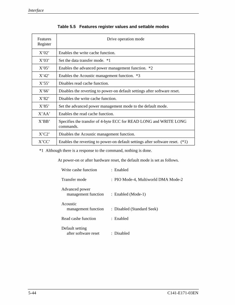
Interface
5-44 C141-E171-03EN
Table 5.5 Features register values and settable modes
FeaturesRegister
Drive operation mode
X’02’ Enables the write cache function.
X’03’ Set the data transfer mode. *1
X’05’ Enables the advanced power management function. *2
X’42’ Enables the Acoustic management function. *3
X’55’ Disables read cache function.
X’66’ Disables the reverting to power-on default settings after software reset.
X’82’ Disables the write cache function.
X’85’ Set the advanced power management mode to the default mode.
X’AA’ Enables the read cache function.
X’BB’ Specifies the transfer of 4-byte ECC for READ LONG and WRITE LONGcommands.
X’C2’ Disables the Acoustic management function.
X’CC’ Enables the reverting to power-on default settings after software reset. (*1)
*1 Although there is a response to the command, nothing is done.
At power-on or after hardware reset, the default mode is set as follows.
Write cashe function : Enabled
Transfer mode : PIO Mode-4, Multiworld DMA Mode-2
Advanced power management function : Enabled (Mode-1)
Acoustic management function : Disabled (Standard Seek)
Read cashe function : Enabled
Default setting after software reset : Disabled

5.3 Host Commands
C141-E171-03EN 5-45
At command issuance (I/O registers setting contents)
1F7H(CM) 1 1 1 0 1 1 1 1
1F6H(DH) x x x DV xx
1F5H(CH)
1F4H(CL)
1F3H(SN)
1F2H(SC)
1F1H(FR)
xx
xx
xx
xx or *1~3
[See Table 5.5]
At command completion (I/O registers contents to be read)
1F7H(ST) Status information
1F6H(DH) x x x DV xx
1F5H(CH)
1F4H(CL)
1F3H(SN)
1F2H(SC)
1F1H(ER)
xx
xx
xx
xx
Error information
*1) Data Transfer Mode
The host sets X’03’ to the Features register. By issuing this command withsetting a value to the Sector Count register, the transfer mode can be selected.Upper 5 bits of the Sector Count register defines the transfer type and lower 3 bitsspecifies the binary mode value.
The IDD supports following values in the Sector Count register value. If othervalue than below is specified, an ABORTED COMMAND error is posted.
PIO default transfer mode 00000 000 (X’00’)
PIO flow control transfer mode X 00001 000 (X’08’: Mode 0)
00001 001 (X’09’: Mode 1)
00001 010 (X’0A’: Mode 2)
00001 011 (X’0B’: Mode 3)
00001 100 (X’0C’: Mode 4)

Interface
5-46 C141-E171-03EN
Multiword DMA transfer mode X 00100 000 (X’20’: Mode 0)
00100 001 (X’21’: Mode 1)
00100 010 (X’22’: Mode 2)
Ultra DMA transfer mode X 01000 000 (X’40’: Mode 0)
01000 001 (X’41’: Mode 1)
01000 010 (X’42’: Mode 2)
01000 011 (X’43’: Mode 3)
01000 100 (X’44’: Mode 4)
01000 101 (X’45’: Mode 5)
*2) Advanced Power Management (APM)
The host writes the Sector Count register with the desired power managementlevel and executes this command with the Features register X’05’, and thenAdvanced Power Management is enabled.
The drive automatically shifts to power saving mode up to the specified APMlevel when the drive does not receive any commands for a specific time. Thesequence in which the power management level shifts is from Active Idle to LowPower Idle to Standby. The Mode-2 level requires the longest shifting time,depending on the APM level settings. The settings of the APM level revert totheir default values when power-on or a hardware or software reset occurs for thedrive.
*3) Automatic Acoustic Management (AAM)
The host writes to the Sector Count register with the requested acousticmanagement level and executes this command with subcommand code 42h, andthen Automatic Acoustic Management is enabled. The AAM level setting ispreserved by the drive across power on, hardware and software resets.
AAM Level Sector Count register
Standard SeekSlow SeekReserved
C0h-FEh, 00h80h-BFh
01h-7Fh, FFh
Standard Seek : Maximum performanceSlow Seek : Minimum acoustic emanation

5.3 Host Commands
C141-E171-03EN 5-47
(15) SET MULTIPLE MODE (X’C6’)
This command enables the device to perform the READ MULTIPLE andWRITE MULTIPLE commands. The block count (number of sectors in ablock) for these commands are also specified by the SET MULTIPLE MODEcommand.
The number of sectors per block is written into the Sector Count register. TheIDD supports 2, 4, 8, 16 and 32 (sectors) as the block counts.
Upon receipt of this command, the device sets the BSY bit of the Status registerand checks the contents of the Sector Count register. If the contents of the SectorCount register is valid and is a supported block count, the value is stored for allsubsequent READ MULTIPLE and WRITE MULTIPLE commands. Executionof these commands is then enabled. If the value of the Sector Count register isnot a supported block count, an ABORTED COMMAND error is posted and theREAD MULTIPLE and WRITE MULTIPLE commands are disabled.
If the contents of the Sector Count register is 0, 1 when the SET MULTIPLEMODE command is issued, the READ MULTIPLE and WRITE MULTIPLEcommands are disabled.
When the SET MULTIPLE MODE command operation is completed, the deviceclears the BSY bit and generates an interrupt.

Interface
5-48 C141-E171-03EN
At command issuance (I/O registers setting contents)
1F7H(CM) 1 1 0 0 0 1 1 0
1F6H(DH) x x x DV xx
1F5H(CH)
1F4H(CL)
1F3H(SN)
1F2H(SC)
1F1H(FR)
xx
xx
xx
Sector count/block
xx
After power-on the READ MULTIPLE and WRITE MULTIPLE commandoperation are disabled as the default mode.
At command completion (I/O registers contents to be read)
1F7H(ST) Status information
1F6H(DH) x x x DV xx
1F5H(CH)
1F4H(CL)
1F3H(SN)
1F2H(SC)
1F1H(ER)
xx
xx
xx
Sector count/block
Error information
(16) SET MAX (F9)
SET MAX Features Register Values
Value Command
00h Obsolete
01h SET MAX SET PASSWORD
02h SET MAX LOCK
03h SET MAX UNLOCK
04h SET MAX FREEZE LOCK
05h - FFh Reserved

5.3 Host Commands
C141-E171-03EN 5-49
• SET MAX ADDRESS
A successful READ NATIVE MAX ADDRESS command shall immediatelyprecede a SET MAX ADDRESS command.
This command allows the maximum address accessible by the user to be set inLBA or CHS mode. Upon receipt of the command, the device sets the BSY bitand saves the maximum address specified in the DH, CH, CL and SN registers.Then, it clears BSY and generates an interrupt.
The new address information set by this command is reflected in Words 1, 54, 57,58, 60 and 61 of IDENTIFY DEVICE information. If an attempt is made toperform a read or write operation for an address beyond the new address space, anID Not Found error will result.
When SC register bit 0, VV (Value Volatile), is 1, the value set by this commandis held even after power on and the occurrence of a hard reset. When the VV bit is0, the value set by this command becomes invalid when the power is turned on ora hard reset occurs, and the maximum address returns to the value (default valueif not set) most lately set when VV bit = 1.
After power on and the occurrence of a hard reset, the host can issue thiscommand only once when VV bit = 1. If this command with VV bit = 1 is issuedtwice or more, any command following the first time will result in an AbortedCommand error.
When the SET MAX ADDRESS EXT command is executed, all SET MAXADRESS commands are aborted. The address value returns to the origin when theSET MAX ADDRESS EXT command is executed using the address valuereturned by the READ NATIVE MAX ADDRESS command.
At command issuance (I/O registers setting contents)
1F7H(CM) 1 1 1 1 1 0 0 1
1F6H(DH) x L x DV Max head/LBA [MSB]
1F5H(CH) Max. cylinder [MSB]/Max. LBA
1F4H(CL) Max. cylinder [LSB]/Max. LBA
1F3H(SN) Max. sector/Max. LBA [LSB]
1F2H(SC) xx VV
1F1H(FR) xx

Interface
5-50 C141-E171-03EN
At command completion (I/O registers contents to be read)
1F7H(ST) Status information
1F6H(DH) x x x DV Max head/LBA [MSB]
1F5H(CH) Max. cylinder [MSB]/Max. LBA
1F4H(CL) Max. cylinder [LSB]/Max. LBA
1F3H(SN) Max. sector/Max. LBA [LSB]
1F2H(SC) xx
1F1H(ER) Error information
• SET MAX SET PASSWORD (FR = 01h)
This command requests a transfer of 1 sector of data from the host, and definesthe contents of SET MAX password. The password is retained by the device untilthe next power cycle.
The READ NATIVE MAX ADDRESS command is not executed just before thiscommand. The command is the SET MAX ADDRESS command if it is thecommand just after the READ NATIVE MAX ADDRESS command is executed.
At command issuance (I/O registers setting contents)
1F7H(CM) 1 1 1 1 1 0 0 1
1F6H(DH) x x x DV xx
1F5H(CH)
1F4H(CL)
1F3H(SN)
xx
xx
xx
1F2H(SC) xx
1F1H(FR) 01

5.3 Host Commands
C141-E171-03EN 5-51
At command completion (I/O registers contents to be read)
1F7H(ST) Status information
1F6H(DH)
1F5H(CH)
1F4H(CL)
1F3H(SN)
1F2H(SC)
xx
xx
xx
xx
xx
1F1H(ER) Error information
Password information
Words Contents
0 Reserved
1 to 16 Password (32 bytes)
17 to 255 Reserved
• SET MAX LOCK (FR = 02h)
The SET MAX LOCK command sets the device into SET_MAX_LOCK state.
After this command is completed, any other SET MAX commands except SETMAX UNLOCK and SET MAX FREEZE LOCK commands are rejected. Andthe device returns command aborted.
The device remains in the SET MAX LOCK state until a power cycle or theacceptance of SET MAX UNLOCK or SET MAX FREEZE LOCK command.
The READ NATIVE MAX ADDRESS command is not executed just before thiscommand. The command is the SET MAX ADDRESS command if it is thecommand just after the READ NATIVE MAX ADDRESS command is executed.

Interface
5-52 C141-E171-03EN
At command issuance (I/O registers setting contents)
1F7H(CM) 1 1 1 1 1 0 0 1
1F6H(DH) x x x DV xx
1F5H(CH)
1F4H(CL)
1F3H(SN)
xx
xx
xx
1F2H(SC) xx
1F1H(FR) 02
At command completion (I/O registers contents to be read)
1F7H(ST) Status information
1F6H(DH)
1F5H(CH)
1F4H(CL)
1F3H(SN)
1F2H(SC)
xx
xx
xx
xx
xx
1F1H(ER) Error information
• SET MAX UNLOCK (FR = 03h)
This command requests a transfer of single sector of data from the host, anddefines the contents of SET MAX ADDRESS password.
The password supplied in the sector of data transferred shall be compared with thestored password.
If the password compare fails, the device returns command aborted anddecrements the Unlock counter, and remains in the Set Max Lock state. On theacceptance of the SET MAX LOCK command, the Unlock counter is set to avalue of five. When this counter reaches zero, then SET MAX UNLOCKcommand returns command aborted until a power cycle.
If the password compare matches, then the device makes a transition to the SetMax Unlocked state and all SET MAX commands will be accepted.
The READ NATIVE MAX ADDRESS command is not executed just before thiscommand. The command is the SET MAX ADDRESS command if it is thecommand just after the READ NATIVE MAX ADDRESS command is executed.

5.3 Host Commands
C141-E171-03EN 5-53
At command issuance (I/O registers setting contents)
1F7H(CM) 1 1 1 1 1 0 0 1
1F6H(DH) x x x DV xx
1F5H(CH)
1F4H(CL)
1F3H(SN)
xx
xx
xx
1F2H(SC) xx
1F1H(FR) 03
At command completion (I/O registers contents to be read)
1F7H(ST) Status information
1F6H(DH)
1F5H(CH)
1F4H(CL)
1F3H(SN)
1F2H(SC)
xx
xx
xx
xx
xx
1F1H(ER) Error information
• SET MAX FREEZE LOCK (FR=04h)
The Set MAX FREEZE LOCK command sets the device to SET_MAX_Frozenstate.
After the device made a transition to the Set Max Freeze Lock state, the followingSET MAX commands are rejected, then the device returns command aborted:
− SET MAX ADDRESS
− SET MAX SET PASSWORD
− SET MAX LOCK
− SET MAX UNLOCK
If the Device is in the SET_MAX_UNLOCK state with the SET MAX FREEZELOCK command, then the device returns command aborted.
The READ NATIVE MAX ADDRESS command is not executed just before thiscommand. The command is the SET MAX ADDRESS command if it is thecommand just after the READ NATIVE MAX ADDRESS command is executed.

Interface
5-54 C141-E171-03EN
At command issuance (I/O registers setting contents)
1F7H(CM) 1 1 1 1 1 0 0 1
1F6H(DH) x x x DV xx
1F5H(CH)
1F4H(CL)
1F3H(SN)
xx
xx
xx
1F2H(SC) xx
1F1H(FR) 04
At command completion (I/O registers contents to be read)
1F7H(ST) Status information
1F6H(DH)
1F5H(CH)
1F4H(CL)
1F3H(SN)
1F2H(SC)
xx
xx
xx
xx
xx
1F1H(ER) Error information
(17) READ NATIVE MAX ADDRESS (F8)
This command posts the maximum address intrinsic to the device, which can beset by the SET MAX ADDRESS command. Upon receipt of this command, thedevice sets the BSY bit and indicates the maximum address in the DH, CH, CLand SN registers. Then, it clears BSY and generates an interrupt.
At command issuance (I/O registers setting contents)
1F7H(CM) 1 1 1 1 1 0 0 0
1F6H(DH) x L x DV xx
1F5H(CH)
1F4H(CL)
1F3H(SN)
1F2H(SC)
1F1H(FR)
xx
xx
xx
xx
xx

5.3 Host Commands
C141-E171-03EN 5-55
At command completion (I/O registers contents to be read)
1F7H(ST) Status information
1F6H(DH) x x x DV Max head/LBA [MSB]
1F5H(CH)
1F4H(CL)
1F3H(SN)
1F2H(SC)
1F1H(ER)
Max. cylinder [MSB]/Max. LBA
Max. cylinder [LSB]/Max. LBA
Max. sector/Max. LBA [LSB]
xx
Error information
(18) EXECUTE DEVICE DIAGNOSTIC (X’90’)
This command performs an internal diagnostic test (self-diagnosis) of the device.This command usually sets the DRV bit of the Drive/Head register is to 0(however, the DV bit is not checked). If two devices are present, both devicesexecute self-diagnosis.
If device 1 is present:
• Both devices shall execute self-diagnosis.
• The device 0 waits for up to 6 seconds until device 1 asserts the PDIAG-signal.
• If the device 1 does not assert the PDIAG- signal but indicates an error, thedevice 0 shall append X’80’ to its own diagnostic status.
• The device 0 clears the BSY bit of the Status register and generates aninterrupt. (The device 1 does not generate an interrupt.)
• A diagnostic status of the device 0 is read by the host system. When adiagnostic failure of the device 1 is detected, the host system can read a statusof the device 1 by setting the DV bit (selecting the device 1).
When device 1 is not present:
• The device 0 posts only the results of its own self-diagnosis.
• The device 0 clears the BSY bit of the Status register, and generates aninterrupt.
Table 5.6 lists the diagnostic code written in the Error register which is 8-bit code.
If the device 1 fails the self-diagnosis, the device 0 “ORs” X’80’ with its ownstatus and sets that code to the Error register.

Interface
5-56 C141-E171-03EN
Table 5.6 Diagnostic code
Code Result of diagnostic
X’01’
X’02’
X’03’
X’04’
X’05’
X’07’
X’08’
X’09’
X’8x’
No error detected.
HDC diagnostic error
Buffer diagnostic error
SRAM diagnostic error
MPU diagnostic error
ROM sum check error
Failure of HDC PVT cell
Failure of HDC DE/ECC
Failure of device 1
attention: The device responds to this command with the result of power-ondiagnostic test.
At command issuance (I/O registers setting contents)
1F7H(CM) 1 0 0 1 0 0 0 0
1F6H(DH) x x x DV Head No. /LBA [MSB]
1F5H(CH)
1F4H(CL)
1F3H(SN)
1F2H(SC)
1F1H(FR)
xx
xx
xx
xx
xx
At command completion (I/O registers contents to be read)
1F7H(ST) Status information
1F6H(DH) x x x DV Head No. /LBA [MSB]
1F5H(CH)
1F4H(CL)
1F3H(SN)
1F2H(SC)
1F1H(ER)
xx
xx
01H (*1)
01H
Diagnostic code
*1 This register indicates X’00’ in the LBA mode.

5.3 Host Commands
C141-E171-03EN 5-57
(19) READ LONG (X’22’ or X’23’)
This command operates similarly to the READ SECTOR(S) command except thatthe device transfers the data in the requested sector and the ECC bytes to the hostsystem. The ECC error correction is not performed for this command. Thiscommand is used for checking ECC function by combining with the WRITELONG command. The READ LONG command supports only single sectoroperation.
Number of ECC bytes to be transferred is fixed to 4 bytes and cannot be changedby the SET FEATURES command.
At command issuance (I/O registers setting contents)
1F7H(CM) 0 0 1 0 0 0 1 R
1F6H(DH) x L x DV Head No. /LBA [MSB]
1F5H(CH)
1F4H(CL)
1F3H(SN)
1F2H(SC)
1F1H(FR)
Cylinder No. [MSB] / LBA
Cylinder No. [LSB] / LBA
Sector No. / LBA [LSB]
01
xx
(R: Retry)
At command completion (I/O registers contents to be read)
1F7H(ST) Status information
1F6H(DH) x L x DV Head No. /LBA [MSB]
1F5H(CH)
1F4H(CL)
1F3H(SN)
1F2H(SC)
1F1H(ER)
Cylinder No. [MSB] / LBA
Cylinder No. [LSB] / LBA
Sector No. / LBA [LSB]
00 (*1)
Error information
*1 If the command is terminated due to an error, this register indicates 01.

Interface
5-58 C141-E171-03EN
(20) WRITE LONG (X’32’ or X’33’)
This command operates similarly to the READ SECTOR(S) command except thatthe device writes the data and the ECC bytes transferred from the host system tothe disk medium. The device does not generate ECC bytes by itself. The WRITELONG command supports only single sector operation.
The number of ECC bytes to be transferred is fixed to 4 bytes and can not bechanged by the SET FEATURES command.
This command is operated under the following conditions:
• READ LONG issued → WRITE LONG (Same address) issues sequence(After READ LONG is issued, WRITE LONG can be issued consecutively.)
If above condition is not satisfied, the WRITE LONG Data becomes theUncorrectable error for subsequence READ command.
At command issuance (I/O registers setting contents)
1F7H(CM) 0 0 1 1 0 0 1 R
1F6H(DH) x L x DV Head No. /LBA [MSB]
1F5H(CH)
1F4H(CL)
1F3H(SN)
1F2H(SC)
1F1H(FR)
Cylinder No. [MSB] / LBA
Cylinder No. [LSB] / LBA
Sector No. / LBA [LSB]
01
xx
At command completion (I/O registers contents to be read)
1F7H(ST) Status information
1F6H(DH) x L x DV Head No. /LBA [MSB]
1F5H(CH)
1F4H(CL)
1F3H(SN)
1F2H(SC)
1F1H(ER)
Cylinder No. [MSB] / LBA
Cylinder No. [LSB] / LBA
Sector No. / LBA [LSB]
00 (*1)
Error information
*1 If the command is terminated due to an error, this register indicates 01.

5.3 Host Commands
C141-E171-03EN 5-59
(21) READ BUFFER (X’E4’)
The host system can read the current contents of the data buffer of the device byissuing this command. Upon receipt of this command, the device sets the BSY bitof Status register and sets up for a read operation. Then the device sets the DRQbit of Status register, clears the BSY bit, and generates an interrupt. After that,the host system can read up to 512 bytes of data from the buffer.
At command issuance (I/O registers setting contents)
1F7H(CM) 1 1 1 1 0 1 0 0
1F6H(DH) x x x DV xx
1F5H(CH)
1F4H(CL)
1F3H(SN)
1F2H(SC)
1F1H(FR)
xx
xx
xx
xx
xx
At command completion (I/O registers contents to be read)
1F7H(ST) Status information
1F6H(DH) x x x DV xx
1F5H(CH)
1F4H(CL)
1F3H(SN)
1F2H(SC)
1F1H(ER)
xx
xx
xx
xx
Error information

Interface
5-60 C141-E171-03EN
(22) WRITE BUFFER (X’E8’)
The host system can overwrite the contents of the data buffer of the device with adesired data pattern by issuing this command. Upon receipt of this command, thedevice sets the BSY bit of the Status register. Then the device sets the DRQ bit ofStatus register and clears the BSY bit when the device is ready to receive the data.After that, 512 bytes of data is transferred from the host and the device writes thedata to the buffer, then generates an interrupt.
At command issuance (I/O registers setting contents)
1F7H(CM) 1 1 1 1 1 0 0 0
1F6H(DH) x x x DV xx
1F5H(CH)
1F4H(CL)
1F3H(SN)
1F2H(SC)
1F1H(FR)
xx
xx
xx
xx
xx
At command completion (I/O registers contents to be read)
1F7H(ST) Status information
1F6H(DH) x x x DV xx
1F5H(CH)
1F4H(CL)
1F3H(SN)
1F2H(SC)
1F1H(ER)
xx
xx
xx
xx
Error information

5.3 Host Commands
C141-E171-03EN 5-61
(23) IDLE (X’97’ or X’E3’)
Upon receipt of this command, the device sets the BSY bit of the Status register,and enters the idle mode. Then, the device clears the BSY bit, and generates aninterrupt. The device generates an interrupt even if the device has not fullyentered the idle mode. If the spindle of the device is already rotating, the spin-upsequence shall not be implemented.
By using this command, the automatic power-down function is enabled and thetimer immediately starts the countdown. When the timer reaches the specifiedvalue, the device enters standby mode.
Enabling the automatic power-down function means that the device automaticallyenters the standby mode after a certain period of time. When the device enters theidle mode, the timer starts countdown. If any command is not issued while thetimer is counting down, the device automatically enters the standby mode. If anycommand is issued while the timer is counting down, the timer is initialized andthe command is executed. The timer restarts countdown after completion of thecommand execution.
The period of timer count is set depending on the value of the Sector Countregister as shown below.
Sector Count register value Point of timer
0 [X’00’] Timeout disabled
1 to 240 [X’01’ to X’F0’] (Value ×5) seconds
241 to 251 [X’F1’ to X’FB’] ((Value-240) ×30) min
252 [X’FC’] 21 minutes
253 [X’FD’] 8 hrs
254 to 255 [X’FE’ to X’FF’] 21 minutes 15 seconds
At command issuance (I/O registers setting contents)
1F7H(CM) X’97’ or X’E3’
1F6H(DH) x x x DV xx
1F5H(CH)
1F4H(CL)
1F3H(SN)
1F2H(SC)
1F1H(FR)
xx
xx
xx
Period of timer
xx

Interface
5-62 C141-E171-03EN
At command completion (I/O registers contents to be read)
1F7H(ST) Status information
1F6H(DH) x x x DV xx
1F5H(CH)
1F4H(CL)
1F3H(SN)
1F2H(SC)
1F1H(ER)
xx
xx
xx
xx
Error information
(24) IDLE IMMEDIATE (X’95’ or X’E1’)
Upon receipt of this command, the device sets the BSY bit of the Status register,and enters the idle mode. Then, the device clears the BSY bit, and generates aninterrupt. This command does not support the automatic power-down function.
At command issuance (I/O registers setting contents)
1F7H(CM) X’95’ or X’E1’
1F6H(DH) x x x DV xx
1F5H(CH)
1F4H(CL)
1F3H(SN)
1F2H(SC)
1F1H(FR)
xx
xx
xx
xx
xx
At command completion (I/O registers contents to be read)
1F7H(ST) Status information
1F6H(DH) x x x DV xx
1F5H(CH)
1F4H(CL)
1F3H(SN)
1F2H(SC)
1F1H(ER)
xx
xx
xx
xx
Error information

5.3 Host Commands
C141-E171-03EN 5-63
(25) STANDBY (X’96’ or X’E2’)
Upon receipt of this command, the device sets the BSY bit of the Status registerand enters the standby mode. The device then clears the BSY bit and generates aninterrupt. The device generates an interrupt even if the device has not fullyentered the standby mode. If the device has already spun down, the spin-downsequence is not implemented.
By using this command, the automatic power-down function is enabled and thetimer starts the countdown when the device returns to idle mode. When the timervalue reaches 0 (a specified time has padded), the device enters standby mode.
Under the standby mode, the spindle motor is stopped. Thus, when the commandinvolving a seek such as the READ SECTOR(s) command is received, the deviceprocesses the command after driving the spindle motor.
At command issuance (I/O registers setting contents)
1F7H(CM) X’96’ or X’E2’
1F6H(DH) x x x DV xx
1F5H(CH)
1F4H(CL)
1F3H(SN)
1F2H(SC)
1F1H(FR)
xx
xx
xx
Period of timer
xx
At command completion (I/O registers contents to be read)
1F7H(ST) Status information
1F6H(DH) x x x DV xx
1F5H(CH)
1F4H(CL)
1F3H(SN)
1F2H(SC)
1F1H(ER)
xx
xx
xx
xx
Error information

Interface
5-64 C141-E171-03EN
(26) STANDBY IMMEDIATE (X’94’ or X’E0’)
Upon receipt of this command, the device sets the BSY bit of the Status registerand enters the standby mode. The device then clears the BSY bit and generates aninterrupt. This command does not support the automatic power-down sequence.
At command issuance (I/O registers setting contents)
1F7H(CM) X’94’ or X’E0’
1F6H(DH) x x x DV xx
1F5H(CH)
1F4H(CL)
1F3H(SN)
1F2H(SC)
1F1H(FR)
xx
xx
xx
xx
xx
At command completion (I/O registers contents to be read)
1F7H(ST) Status information
1F6H(DH) x x x DV xx
1F5H(CH)
1F4H(CL)
1F3H(SN)
1F2H(SC)
1F1H(ER)
xx
xx
xx
xx
Error information

5.3 Host Commands
C141-E171-03EN 5-65
(27) SLEEP (X’99’ or X’E6’)
This command is the only way to make the device enter the sleep mode.
Upon receipt of this command, the device sets the BSY bit of the Status registerand enters the sleep mode. The device then clears the BSY bit and generates aninterrupt. The device generates an interrupt even if the device has not fullyentered the sleep mode.
In the sleep mode, the spindle motor is stopped and the ATA interface section isinactive. All I/O register outputs are in high-impedance state.
The only way to release the device from sleep mode is to execute a software orhardware reset.
At command issuance (I/O registers setting contents)
1F7H(CM) X’99’ or X’E6’
1F6H(DH) x x x DV xx
1F5H(CH)
1F4H(CL)
1F3H(SN)
1F2H(SC)
1F1H(FR)
xx
xx
xx
xx
xx
At command completion (I/O registers contents to be read)
1F7H(ST) Status information
1F6H(DH) x x x DV xx
1F5H(CH)
1F4H(CL)
1F3H(SN)
1F2H(SC)
1F1H(ER)
xx
xx
xx
xx
Error information
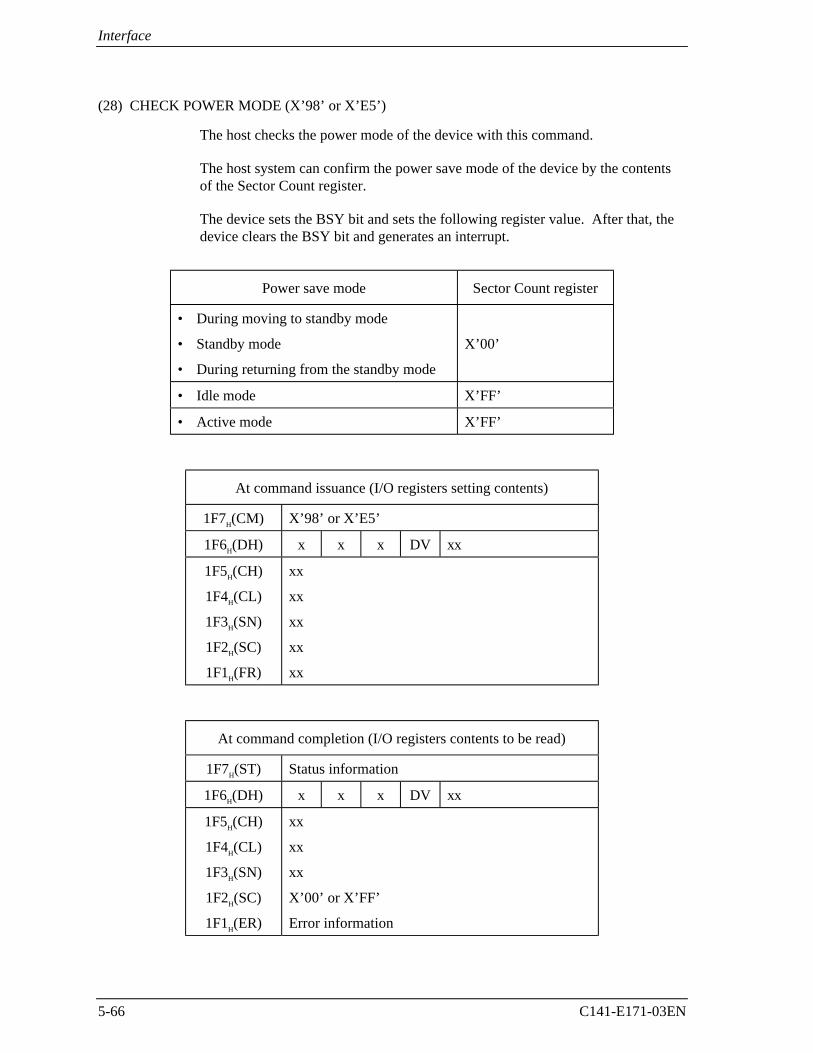
Interface
5-66 C141-E171-03EN
(28) CHECK POWER MODE (X’98’ or X’E5’)
The host checks the power mode of the device with this command.
The host system can confirm the power save mode of the device by the contentsof the Sector Count register.
The device sets the BSY bit and sets the following register value. After that, thedevice clears the BSY bit and generates an interrupt.
Power save mode Sector Count register
• During moving to standby mode
• Standby mode
• During returning from the standby mode
X’00’
• Idle mode X’FF’
• Active mode X’FF’
At command issuance (I/O registers setting contents)
1F7H(CM) X’98’ or X’E5’
1F6H(DH) x x x DV xx
1F5H(CH)
1F4H(CL)
1F3H(SN)
1F2H(SC)
1F1H(FR)
xx
xx
xx
xx
xx
At command completion (I/O registers contents to be read)
1F7H(ST) Status information
1F6H(DH) x x x DV xx
1F5H(CH)
1F4H(CL)
1F3H(SN)
1F2H(SC)
1F1H(ER)
xx
xx
xx
X’00’ or X’FF’
Error information

5.3 Host Commands
C141-E171-03EN 5-67
(29) SMART (X’B0)
This command predicts the occurrence of device failures depending on thesubcommand specified in the FR register. If the FR register contains values thatare not supported with the command, the Aborted Command error is issued.
Before issuing the command, the host must set the key values in the CL and CHregisters (4Fh in the CL register and C2h in the CH register). If the key valuesare incorrect, the Aborted Command error is issued.
If the failure prediction function is disabled, the device returns the AbortedCommand error to subcommands other than those of the SMART EnableOperations (with the FR register set to D8h).
If the failure prediction function is enabled, the device collects and updates dataon specific items. The values of items whose data is collected and updated by thedevice in order to predict device failures are hereinafter referred to as attributevalues.

Interface
5-68 C141-E171-03EN
Table 5.7 Features Register values (subcommands) and functions (1 of 3)
Features Resister Function
X’D0’ SMART Read Attribute Values:A device that received this subcommand asserts the BSY bit and saves allthe updated attribute values. The device then clears the BSY bit andtransfers 512-byte attribute value information to the host.* For information about the format of the attribute value information, see
Table 5.8.
X’D1’ SMART Read Attribute Thresholds:This subcommand is used to transfer 512-byte insurance failure thresholdvalue data to the host.* For information about the format of the insurance failure threshold value
data, see Table 5.9.
X’D2’ SMART Enable/Disable Attribute AutoSave:
Enables (by setting the SC register to a value other than 00h) or disables (bysetting the SC register to 00h) a function that automatically saves deviceattribute values (“automatic attribute save function”). This setting is heldregardless of whether the device is turned on or off. If the automaticattribute save function is enabled and more than 15 minutes has elapsedsince the last time that attributes were saved, then the attributes are saved.However, if the automatic attribute save function is disabled, the attributesare not saved. Upon receiving this subcommand, a device asserts BSY,enables or disables the automatic attribute save function, and clears BSY.
X’D3’ SMART Save Attribute Values:When the device receives this subcommand, it asserts the BSY bit, savesdevice attribute value data, then clears the BSY bit.
X’D4’ SMART Executive Off-line Immediate:A device which receives this command asserts the BSY bit, then startscollecting the off-line data specified in the SN register, or stops.In the off-line mode, after BSY is cleared, off-line data are collected. In thecaptive mode, it collects off-line data with the BSY assertion as is, thenclears the BSY when collection of data is completed.
SN Off-line data collection mode00h: Off-line diagnosis (off-line mode)01h: Simple self test (off-line mode)02h: Comprehensive self test (off-line mode)7Fh: Self test stop81h: Simple self test (captive mode)82h: Comprehensive self test (captive mode)

5.3 Host Commands
C141-E171-03EN 5-69
Table 5.7 Features Register values (subcommands) and functions (2 of 3)
Features Resister Function
X’D5’ SMART Read Log Sector:A device which receives this sub-command asserts the BSY bit, then readsthe log sector specified in the SN register. Next, it clears the BSY bit andtransmits the log sector to the host computer.
SN: SC: Log sector00h: 01h: SMART log directory01h: 01h: SMART summary error log02h: 33h: SMART comprehensive error log06h: 01h: SMART self test log80h-9Fh: 01h-10h: Host vendor log
* See Table 5.11 concerning the SMART error log data format.See Table 5.12 concerning the SMART self test log data format.
X’D6’ SMART Write Log Sector:A device which receives this sub-command asserts the BSY bit and when ithas prepared to receive data from the host computer, it sets DRQ and clearsthe BSY bit. Next, it receives data from the host computer and writes thespecified log sector in the SN register.
SN: SC: Log sector80h-9Fh: 01h-10h Host vendor log
* The host can write any desired data in the host vendor log.
X’D8’ SMART Enable Operations:This subcommand enables the failure prediction feature. The setting ismaintained even when the device is turned off and then on.When the device receives this subcommand, it asserts the BSY bit, enablesthe failure prediction feature, then clears the BSY bit.
X’D9’ SMART Disable Operations:This subcommand disables the failure prediction feature. The setting ismaintained even when the device is turned off and then on.When the device receives this subcommand, it asserts the BSY bit, disablesthe failure prediction feature, then clears the BSY bit.

Interface
5-70 C141-E171-03EN
Table 5.7 Features Register values (subcommands) and functions (3 of 3)
Features Resister Function
X’DA’ SMART Return Status:When the device receives this subcommand, it asserts the BSY bit and saves thecurrent device attribute values. Then the device compares the device attributevalues with insurance failure threshold values. If there is an attribute valueexceeding the threshold, F4h and 2Ch are loaded into the CL and CH registers.If there are no attribute values exceeding the thresholds, 4Fh and C2h are loadedinto the CL and CH registers. After the settings for the CL and CH registershave been determined, the device clears the BSY bit
X’DB’ SMART Enable/Disable Auto Off-line:This sets automatic off-line data collection in the enabled (when the SCregister specification ≠ 00h) or disabled (when the SC register specification= 00) state. This setting is preserved whether the drive’s power is switchedon or off.If 24 hours have passed since the power was switched on, or since the lasttime that off-line data were collected, off-line data collection is performedwithout relation to any command from the host computer.
The host must regularly issue the SMART Read Attribute Values subcommand(FR register = D0h), SMART Save Attribute Values subcommand (FR register =D3h), or SMART Return Status subcommand (FR register = DAh) to save thedevice attribute value data on a medium.
Alternative, the device must issue the SMART Enable-Disable AttributeAutoSave subcommand (FR register = D2h) to use a feature which regularly savethe device attribute value data to a medium.
The host can predict failures in the device by periodically issuing the SMART ReturnStatus subcommand (FR register = DAh) to reference the CL and CH registers.
If an attribute value is below the insurance failure threshold value, the device isabout to fail or the device is nearing the end of its life . In this case, the hostrecommends that the user quickly backs up the data.
At command issuance (I-O registers setting contents)
1F7H(CM) 1 0 1 1 0 0 0 0
1F6H(DH) x x x DV xx
1F5H(CH)
1F4H(CL)
1F3H(SN)
1F2H(SC)
1F1H(FR)
Key (C2h)
Key (4Fh)
xx
xx
Subcommand

5.3 Host Commands
C141-E171-03EN 5-71
At command completion (I-O registers setting contents)
1F7H(ST) Status information
1F6H(DH) x x x DV xx
1F5H(CH)
1F4H(CL)
1F3H(SN)
1F2H(SC)
1F1H(ER)
Key-failure prediction status (C2h/2Ch)
Key-failure prediction status (4Fh/F4h)
xx
xx
Error information
The attribute value information is 512-byte data; the format of this data is shownthe following table 5.8. The host can access this data using the SMART ReadAttribute Values subcommand (FR register = D0h). The insurance failurethreshold value data is 512-byte data; the format of this data is shown thefollowing table 5.9. The host can access this data using the SMART ReadAttribute Thresholds subcommand (FR register = D1h).

Interface
5-72 C141-E171-03EN
Table 5.8 Format of device attribute value data
Byte Item
00
01
Data format version number
02 Attribute 1 Attribute ID
03
04
Status flag
05 Current attribute value
06 Attribute value for worst case so far
07 to 0C Raw attribute value
0D Reserved
0E to 169 Attribute 2 toattribute 30
(The format of each attribute value is the same asthat of bytes 02 to 0D.)
16A Off-line data collection status
16B Self test execution status
16C, 16D Off-line data collection execution time [sec.]
16E Reserved
16F Off-line data collection capability
170, 171 Trouble prediction capability flag
172 Error logging capability
173 (Self test error detection point)
174 Simple self test (Quick Test) execution time [min.]
175 Comprehensive self test (Comprehensive Test) execution time [min.]
176 to 181 Reserved
182 to 1FE Vendor unique
1FF Check sum
Table 5.9 Format of insurance failure threshold value data
Byte Item
00
01
Data format version number
02 Threshold 1 Attribute ID
03 Insurance failure threshold
04 to 0D Reserved
0E to 169 Threshold 2 toThreshold 30
(The format of each threshold value is the same asthat of bytes 02 to 0D.)
16A to 17B Reserved
17C to 1FE Vendor unique
1FF Check sum

5.3 Host Commands
C141-E171-03EN 5-73
• Data format version number
The data format version number indicates the version number of the dataformat of the device attribute values or insurance failure thresholds. The dataformat version numbers of the device attribute values and insurance failurethresholds are the same. When a data format is changed, the data formatversion numbers are updated.
• Attribute ID
The attribute ID is defined as follows:
Attribute ID Attribute name
0 (Indicates unused attribute data.)
1 Read Error Rate
2 Throughput Performance
3 Spin Up Time
4 Start/Stop Count
5 Reallocated Sector Count
7 Seek Error Rate
8 Seek Time Performance
9 Power-On Hours Count
10 Spin Retry Count
12 Drive Power Cycle Count
192 Emergency Retract Cycle Count
193 Load/Unload Cycle Count
194 HDA Temperature
195 ECC On the Flag Count
196 Reallocated Event Count
197 Current Pending Sector Count
198 Off-Line Scan Uncorrectable Sector Count
199 Ultra ATA CRC Error Count
200 Write Error Rate
203 Run Out

Interface
5-74 C141-E171-03EN
• Status Flag
Bit Meaning
0 If this bit is 1, it indicates normal operations are assured with theattribute when the attribute value exceeds the threshold value.
1 If this bit is 1 (0), it indicates the attribute only updated by an on-line test (off-line test).
2 If this bit 1, it indicates the attribute that represents performance.
3 If this bit 1, it indicates the attribute that represents an error rate.
4 If this bit 1, it indicates the attribute that represents thenumber of occurrences.
5 If this bit 1, it indicates the attribute that can be collected/savedeven if the drive fault prediction function is disabled.
6 to 15 Reserve bit
• Current attribute value
It indicates the normalized value of the original attribute value. The valuedeviates in a range of 01h to 64h (range of 01h to C8h for the ultra ATA CRCerror rate). It indicates that the closer the value is to 01h, the higher thepossibility of a failure. The host compares the attribute value with thethreshold value. If the attribute value is larger than the threshold value, thedrive is determined to be normal.
• Attribute value for the worst case so far
This is the worst attribute value among the attribute values collected to date.This value indicates the state nearest to a failure so far.
• Raw attribute value
Raw attributes data is retained.
• Off-line data collection status

5.3 Host Commands
C141-E171-03EN 5-75
Status Byte Meaning
00h or 80h Off-line data acquisition is not executed.02h or 82h Off-line data acquisition has ended without an error.04h or 84h Off-line data acquisition is interrupted by a command from the host.05h or 85h Off-line data acquisition has ended before completion because of a
command from the host.06h or 86h Off-line data acquisition has ended before completion because of an
error that makes acquisition impossible. (Not used)
40 to 7Fh Vendor unique (Not used)C0h to FFh
01h or 81h03h or 83h07h or 3Fh87h to BFh
Reserved
• Self test execution status
Bit Meaning
0 to 3: Remainder of the self-test is indicated as a percentage in a rangeof "0h to 9h" (corresponding to 0 to 90%).
4 to 7: Self-test execution status
= 0h: Self-test has ended successfully, or self-test has not beenexecuted.
= 1h: Self-test is suspended by the host.
= 2h: Self-test is interrupted by a soft/hard reset from the host.
= 3h: Self-test cannot be executed.
= 4h: Self-test has ended with an abnormality because of unknowncontents.
= 5h: Self-test has ended with "Write/Read Test" error.
= 6h: Self-test has ended with "Servo Check," "Pre-SMART Check," or"Post-SMART Check" error.
= 7h: Self-test has ended with "SMART Drive Error Log Check,""Random Read Test," or "Read Scan Test" error.
= 8h: Reserved
= 9h: Reserved
= Ah: Reserved
= Bh: Reserved
= Ch to Eh: Reserved
= Fh: Self-test is in progress.

Interface
5-76 C141-E171-03EN
• Off-line data collection capability
Indicates the method of off-line data collection carried out by the drive. Ifthe off-line data collection capability is 0, it indicates that off-line datacollection is not supported.
Bit Meaning
0 If this bit is 1, it indicates that the SMART EXECUTE OFF-LINE IMMEDATE sub-command (FR register = D4h) issupported.
1 Vendor unique
2 If this bit is 1, it indicates that acquisition of off-line dataunder execution is aborted when a new command is received.
3 If this bit is 1, it indicates that the SMART Off-line ReadScanning Technology is supported.
4 If this bit is 1, it indicates that the SMART Self-test functionis supported.
5 to 7 Reserved bits
• Failure prediction capability flag
Bit Meaning
0 If this bit is 1, it indicates that the attribute value is saved onmedia before the drive enters the power save mode.
1 If this bit is 1, it indicates that the attribute value is savedautomatically after the pre-set operation of the drive.
2 to 15 Reserved bits
• Error logging capability
Bit Meaning
0 If this bit is 1, it indicates that the drive error loggingfunction is supported.
1 to 7 Reserved bits
• Check sum
Two’s complement of the lower byte, obtained by adding 511-byte data onebyte at a time from the beginning.

5.3 Host Commands
C141-E171-03EN 5-77
• Insurance failure threshold
The limit of a varying attribute value. The host compares the attribute valueswith the thresholds to identify a failure.
Table 5.10 Log Directory Data Format
Byte Item
0001
SMART Logging Version
02 Number of sectors of Address "01h"
0304
05-0B
ReservedNumber of sectors of Address "02h"Reserved
0C Number of sectors of Address "06h"
0D
FFReserved
100 Number of sector
101Address 80h
Reserved
102
13F
Address 81h
Address 9Fh
"102" and "13F" are both the sameformat as "100-101"
140
1FFReserved
• SMART error logging
If the device detects an unrecoverable error during execution of a commandreceived from the host, the device registers the error information in the SMARTSummary Error Log (see Table ...) and the SMART Comprehensive Error Log(see Table ...), and saves the information on media.
The host issues the SMART Read Log Sector sub-command (FR register = D5h,SN register = 01h, SC register = 01h) and can read the SMART Summary ErrorLog.
The host issues the SMART Read Log Sector sub-command (FR register = D5h,SN register = 02h, SC register = 33h) and can read the SMART ComprehensiveError Log.

Interface
5-78 C141-E171-03EN
Table 5.11 Data format of SMART Summary Error Log
Byte Item
00 Version of this function
01 Pointer for the latest "Error Log Data Structure"
02 to 31 Reserved
32 Device Control register value
33 Features register value
34 Sector Count register value
35 Sector Number register value
36 Cylinder Low register value
37 Cylinder High register value
38 Drive/Head register value
39 Command register value
3A to 3D
Command datastructure
Elapsed time after the power-onsequence (unit: ms)
3E Reserved
3F Error register value
40 Sector Count register value
41 Sector Number register value
42 Cylinder Low register value
43 Cylinder High register value
44 Drive/Head register value
45 Status register value
46 to 58 Vendor unique
59 State
5A5B
Error log datastructure
Error datastructure
Power-on time (unit: h)
5C to 1C3 Error log datastructure 2 toError log data
structure 5
Format of each error log data structure is same as those ofbytes 02 to 5B.
1C4, 1C5 Number of unrecoverable errors that have occurred.
1C6 to 1FE Reserved
1FF Check sum

5.3 Host Commands
C141-E171-03EN 5-79
• Command data structure
Indicates the command received when an error occurs.
• Error data structure
Indicates the status register when an error occurs.
• Total number of drive errors
Indicates total number of errors registered in the error log.
• Checksum
Two's complementary for the lowest-order 1 byte that is obtained by adding 1byte after another for as many as 511 bytes beginning from the top of thestructure.
• Status
Bits 0 to 3: Indicates the drive status when received error commandsaccording to the following table.
Bits 4 to 7: Vendor unique
Status Meaning
0 Unclear status
1 Sleep status
2 Standby status
3 Active status or idle status (BSY bit = 0)
4 Off-line data collection being executed
5 to F Reserved
Table 5.11.1 Data format of SMART Comprehensive Error Log
Byte First sector Next sector
00h SMART Error Logging 01h Reserved
01h Index Pointer Latest Error Data Structure. Reserved
02h...5Bh 1st Error Log Data Structure Data Structure 5n + 1
5Ch...B5h 2nd Error Log Data Structure Data Structure 5n + 2
B6h...10Fh 3rd Error Log Data Structure Data Structure 5n + 3
110h...169h 4th Error Log Data Structure Data Structure 5n + 4
16Ah...1C3h 5th Error Log Data Structure Data Structure 5n + 5
1C4h...1C5h Total Error Count Reserved
1C6h...1FEh Reserved Reserved
1FFh Checksum Checksum

Interface
5-80 C141-E171-03EN
• SMART Self Test
The host computer can issue the SMART Execute Off-line Immediate sub-command (FR Register = D4h) and cause the device to execute a self test. Whenthe self test is completed, the device saves the SMART self test log to the diskmedium.
The host computer can issue the SMART Read Log Sector sub-command (FRRegister = D5h, SN Register = 06h, SC register = 01h) and can read the SMARTself test log.
Table 5.12 SMART self test log data format
Byte Item
00, 01 Self test log data structure
02 Self test log 1 Self test number (SN Register Value)
03 Self test execution status
04, 05 Life time. Total power-on time [hours]
06 Self test error No.
07 to 0A Error LBA
0B to 19 Vendor unique
1A to 1F9 Self test log 2 to 21 (Each log data format is the same as that inbyte 02 to 19.)
1FA, 1FB Vendor unique
1FC Self test index
1FD, 1FE Reserved
1FF Check sum
• Self-test number
Indicates the type of self-test executed.
• Self-test execution status
Same as byte 16Bh of the attribute value.
• Self-test index
If this is "00h", it indicates the status where the self-test has never beenexecuted.
• Checksum
Two's complementary for the lowest-order 1 byte that is obtained by adding 1byte after another for as many as 511 bytes from the top.

5.3 Host Commands
C141-E171-03EN 5-81
(30) SECURITY DISABLE PASSWORD (F6h)
This command invalidates the user password already set and releases the lockfunction.
The host transfers the 512-byte data shown in Table 5.13 to the device. Thedevice compares the user password or master password in the transferred datawith the user password or master password already set, and releases the lockfunction if the passwords are the same.
Although this command invalidates the user password, the master password isretained. To recover the master password, issue the SECURITY SETPASSWORD command and reset the user password.
If the user password or master password transferred from the host does not match,the Aborted Command error is returned.
Issuing this command while in LOCKED MODE or FROZEN MODE returns theAborted Command error.
(The section about the SECURITY FREEZE LOCK command describesLOCKED MODE and FROZEN MODE.)

Interface
5-82 C141-E171-03EN
Table 5.13 Contents of security password
Word Contents
0 Control word
Bit 0: Identifier
0 = Compares the user passwords.
1 = Compares the master passwords.
Bits 1 to 15: Reserved
1 to 16 Password (32 bytes)
17 to 255 Reserved
At command issuance (I-O register contents))
1F7h(CM) 1 1 1 1 0 1 1 0
1F6h(DH) x x x DV xx
1F5h(CH)
1F4h(CL)
1F3h(SN)
1F2h(SC)
1F1h(FR)
xx
xx
xx
xx
xx
At command completion (I-O register contents)
1F7h(ST) Status information
1F6h(DH) x x x DV xx
1F5h(CH)
1F4h(CL)
1F3h(SN)
1F2h(SC)
1F1h(ER)
xx
xx
xx
xx
Error information

5.3 Host Commands
C141-E171-03EN 5-83
(31) SECURITY ERASE PREPARE (F3h)
The SECURITY ERASE UNIT command feature is enabled by issuing theSECURITY ERASE PREPARE command and then the SECURITY ERASEUNIT command. The SECURITY ERASE PREPARE command prevents datafrom being erased unnecessarily by the SECURITY ERASE UNIT command.
Issuing this command during FROZEN MODE returns the Aborted Commanderror.
At command issuance (I-O register contents)
1F7h(CM) 1 1 1 1 0 0 1 1
1F6h(DH) x x x DV xx
1F5h(CH)
1F4h(CL)
1F3h(SN)
1F2h(SC)
1F1h(FR)
xx
xx
xx
xx
xx
At command completion (I-O register contents)
1F7h(ST) Status information
1F6h(DH) x x x DV xx
1F5h(CH)
1F4h(CL)
1F3h(SN)
1F2h(SC)
1F1h(ER)
xx
xx
xx
xx
Error information
(32) SECURITY ERASE UNIT (F4h)
This command erases all user data. This command also invalidates the userpassword and releases the lock function.
The host transfers the 512-byte data shown in Table 5.13 to the device. Thedevice compares the user password or master password in the transferred datawith the user password or master password already set. The device erases userdata, invalidates the user password, and releases the lock function if thepasswords are the same.

Interface
5-84 C141-E171-03EN
Although this command invalidates the user password, the master password isretained. To recover the master password, issue the SECURITY SETPASSWORD command and reset the user password.
If the SECURITY ERASE PREPARE command is not issued immediately beforethis command is issued, the Aborted Command error is returned.
Issuing this command while in FROZEN MODE returns the Aborted Commanderror.
At command issuance (I-O register contents)
1F7h(CM) 1 1 1 1 0 1 0 0
1F6h(DH) x x x DV xx
1F5h(CH)
1F4h(CL)
1F3h(SN)
1F2h(SC)
1F1h(FR)
xx
xx
xx
xx
xx
At command completion (I-O register contents)
1F7h(ST) Status information
1F6h(DH) x x x DV xx
1F5h(CH)
1F4h(CL)
1F3h(SN)
1F2h(SC)
1F1h(ER)
xx
xx
xx
xx
Error information
(33) SECURITY FREEZE LOCK (F5h)
This command puts the device into FROZEN MODE. The following commandsused to change the lock function return the Aborted Command error if the deviceis in FROZEN MODE.
• SECURITY SET PASSWORD
• SECURITY UNLOCK
• SECURITY DISABLE PASSWORD
• SECURITY ERASE PREPARE

5.3 Host Commands
C141-E171-03EN 5-85
• SECURITY ERASE UNIT
FROZEN MODE is canceled when the power is turned off, or when hardware isreseted. If this command is reissued in FROZEN MODE, the command iscompleted and FROZEN MODE remains unchanged.
Issuing this command during LOCKED MODE returns the Aborted Commanderror.
The following medium access commands return the Aborted Command errorwhen the device is in LOCKED MODE:
• READ DMA (EXT)
• READ LONG
• READ MULTIPLE (EXT)
• READ SECTORS
• READ VERIFY SECTORS
• WRITE DMA (EXT)
• WRITE LONG
• WRITE MULTIPLE (EXT)
• WRITE SECTORS (EXT)
• WRITE VERIFY
• SECURITY DISABLE PASSWORD
• SECURITY FREEZE LOCK
• SECURITY SET PASSWORD
• SET MAX ADDRESS (EXT)
• FLUSH CACHE (EXT)
• DCO RESTORE
• DCO SET
• SET MAX ADDRESS (EXT)
At command issuance (I-O register contents)
1F7h(CM) 1 1 1 1 0 1 0 1
1F6h(DH) x x x DV xx
1F5h(CH)
1F4h(CL)
xx
xx

Interface
5-86 C141-E171-03EN
1F3h(SN)
1F2h(SC)
1F1h(FR)
xx
xx
xx
At command completion (I-O register contents)
1F7h(ST) Status information
1F6h(DH) x x x DV xx
1F5h(CH)
1F4h(CL)
1F3h(SN)
1F2h(SC)
1F1h(ER)
xx
xx
xx
xx
Error information
(34) SECURITY SET PASSWORD (F1h)
This command enables a user password or master password to be set.
The host transfers the 512-byte data shown in Table 5.14 to the device. Thedevice determines the operation of the lock function according to thespecifications of the Identifier bit and Security level bit in the transferred data.(Table 5.15)
Issuing this command in LOCKED MODE or FROZEN MODE returns theAborted Command error.
Table 5.14 Contents of SECURITY SET PASSWORD data
Word Contents
0 Control wordBit 0 Identifier
0 = Sets a user password.1 = Sets a master password.
Bits 1 to 7 ReservedBit 8 Security level
0 = High1 = Maximum
Bits 9 to 15 Reserved
1 to 16 Password (32 bytes)
17 Master password version number
18 to 255 Reserved

5.3 Host Commands
C141-E171-03EN 5-87
Table 5.15 Relationship between combination of Identifier and Security level, andoperation of the lock function
Identifier Level Description
User High The specified password is saved as a new user password.The lock function is enabled after the device is turned offand then on. LOCKED MODE can be canceled using theuser password or the master password already set.
Master High The specified password is saved as a new master password.The lock function is not enabled.
User Maximum The specified password is saved as a new user password.The lock function is enabled after the device is turned offand then on. LOCKED MODE can be canceled using theuser password only. The master password already setcannot cancel LOCKED MODE.
Master Maximum The specified password is saved as a new master password.The lock function is not enabled.
At command issuance (I-O register contents)
1F7h(CM) 1 1 1 1 0 0 0 1
1F6h(DH) x x x DV xx
1F5h(CH)
1F4h(CL)
1F3h(SN)
1F2h(SC)
1F1h(FR)
xx
xx
xx
xx
xx
At command completion (I-O register contents)
1F7h(ST) Status information
1F6h(DH) x x x DV xx
1F5h(CH)
1F4h(CL)
1F3h(SN)
1F2h(SC)
1F1h(ER)
xx
xx
xx
xx
Error information

Interface
5-88 C141-E171-03EN
(35) SECURITY UNLOCK
This command cancels LOCKED MODE.
The host transfers the 512-byte data shown in Table 5.13 to the device. Operationof the device varies as follows depending on whether the host specifies the masterpassword.
• When the master password is selected
When the security level is LOCKED MODE is high, the password iscompared with the master password already set. If the passwords are thesame, LOCKED MODE is canceled. Otherwise, the Aborted Command erroris returned. If the security level in LOCKED MODE is set to the highestlevel, the Aborted Command error is always returned.
• When the user password is selected
The password is compared with the user password already set. If thepasswords are the same, LOCKED MODE is canceled. Otherwise, theAborted Command error is returned.
If the password comparison fails, the device decrements the UNLOCK counter.The UNLOCK counter initially has a value of five. When the value of theUNLOCK counter reaches zero, this command or the SECURITY ERASE UNITcommand causes the Aborted Command error until the device is turned off andthen on, or until a hardware reset is executed. Issuing this command withLOCKED MODE canceled (in UNLOCK MODE) has no affect on the UNLOCKcounter.
Issuing this command in FROZEN MODE returns the Aborted Command error.
At command issuance (I-O register contents)
1F7h(CM) 1 1 1 1 0 0 1 0
1F6h(DH) x x x DV xx
1F5h(CH)
1F4h(CL)
1F3h(SN)
1F2h(SC)
1F1h(FR)
xx
xx
xx
xx
xx

5.3 Host Commands
C141-E171-03EN 5-89
At command completion (I-O register contents)
1F7h(ST) Status information
1F6h(DH) x x x DV xx
1F5h(CH)
1F4h(CL)
1F3h(SN)
1F2h(SC)
1F1h(ER)
xx
xx
xx
xx
Error information
(36) FLUSH CACHE (E7)
This command is used to order to write every write cache data stored by thedevice into the medium. BSY bit is held at "1" until every data has been writtennormally or an error has occurred. The device performs every error recovery sothat the data are read correctly.
When executing this command, the reading of the data may take several secondsif much data are to be read.
In case a non-recoverable error has occurred while the data is being read, the errorgeneration address is put into the command block register before ending thecommand. This error sector is deleted from the write cache data, and theremaining cache data is written into the medium by the execution of the nextFlush Cache command.
At command issuance (I-O register contents)
1F7h(CM) 1 1 1 0 0 1 1 1
1F6h(DH) x x x DV xx
1F5h(CH)
1F4h(CL)
1F3h(SN)
1F2h(SC)
1F1h(FR)
xx
xx
xx
xx
xx

Interface
5-90 C141-E171-03EN
At command completion (I-O register contents to be read)
1F7h(ST) Status information
1F6h(DH) x x x DV xx
1F5h(CH)
1F4h(CL)
1F3h(SN)
1F2h(SC)
1F1h(ER)
xx
xx
xx
xx
Error information
(37) DEVICE CONFIGURATION (X'B1')
Individual Device Configuration Overlay feature set commands are identified bythe value placed in the Features register. The following table shows theseFeatures register values. If this command sets with the reserved value of Featuresregister, an aborted error is posted.
FR values Command
C0h DEVICE CONFIGURATION RESTORE
C1h DEVICE CONFIGURATION FREEZE
C2h DEVICE CONFIGURATION IDENTIFY
C3h DEVICE CONFIGURATION SET
00h-BFh, C4h-FFh Reserved
At command issuance (I-O register contents)
1F7h(CM) 1 0 1 1 0 0 0 1
1F6h(DH) x x x DV xx
1F5h(CH)
1F4h(CL)
1F3h(SN)
1F2h(SC)
1F1h(FR)
xx
xx
xx
xx
C0h/C1h/C2h/C3h

5.3 Host Commands
C141-E171-03EN 5-91
At command completion (I-O register contents)
1F7h(ST) Status information
1F6h(DH) x x x DV xx
1F5h(CH)
1F4h(CL)
1F3h(SN)
1F2h(SC)
1F1h(ER)
xx
xx
xx
xx
Error information
• DEVICE CONFIGURATION RESTORE (FR=C0h)
The DEVICE CONFIGURATION RESTORE command disables any settingpreviously made by a DEVICE CONFIGURATION SET command andreturns the content of the IDENTIFY DEVICE command response to theoriginal settings as indicated by the data returned from the execution of aDEVICE CONFIGURATION IDENTIFY command. After execution of thiscommand, the settings are kept for the device power down or reset.
If a Host Protected Area has been set by a SET MAX ADDRESS (EXT)command, or if DEVICE CONFIGURATION FREEZE LOCK is set, anaborted error is posted.
• DEVICE CONFIGURATION FREEZE LOCK (FR=C1h)
The DEVICE CONFIGURATION FREEZE LOCK command preventsaccidental modification of the Device Configuration Overlay settings. Aftersuccessful execution of a DEVICE CONFIGURATION FREEZE LOCKcommand, all DEVICE CONFIGURATION SET, DEVICECONFIGURATION FREEZE LOCK, DEVICE CONFIGURATIONIDENTIFY, and DEVICE CONFIGURATION RESTORE commands areaborted by the device. The DEVICE CONFIGURATION FREEZE LOCKcondition is cleared by a power-down, not cleared by a hardware or softwarereset.
If the device has executed a previous DEVICE CONFIGURATION FREEZELOCK command since power-up, an aborted error is posted.

Interface
5-92 C141-E171-03EN
• DEVICE CONFIGURATION IDENTIFY (FR=C2h)
The DEVICE CONFIGURATION IDENTIFY command returns a 512 bytedata structure is shown in Table 5.16. The content of this data structureindicates the selectable commands, modes, and feature sets that the device iscapable of supporting. If a DEVICE CONFIGURATION SET command hasbeen issued reducing the capabilities, the response to an IDENTIFY DEVICEcommand will reflect the reduced set of capabilities, while the DEVICECONFIGURATION IDENTIFY command will reflect the entire set ofselectable capabilities.
If the device has executed a previous DEVICE CONFIGURATION FREEZELOCK command since power-up, an aborted error is posted.
• DEVICE CONFIGURATION SET (FR=C3h)
The DEVICE CONFIGURATION SET command allows to reduce the set ofoptional commands, modes, or feature sets supported by a device as indicatedby a DEVICE CONFIGURATION IDENTIFY command. The format of theoverlay transmitted by the device is described in Table 5.16. The DEVICECONFIGURATION SET command transfers an overlay that modifies someof the bits set in words 63, 82, 83, 84, and 88 of the IDENTIFY DEVICEcommand response. When the bits in these words are cleared, the device nolonger supports the indicated command, mode, or feature set. If a bit is set inthe overlay transmitted by the device that is not set in the overlay receivedfrom a DEVICE CONFIGURATION IDENTIFY command, no action istaken for that bit. After execution of this command, the settings are kept forthe device power down or reset.
If the restriction of Multiword DMA modes or Ultra DMA modes isexecuted, a SET FEATURES command should be issued for the modesrestriction prior the DEVICE CONFIGURATION SET command is issued.
If a DEVICE CONFIGURATION SET command has already modified theoriginal settings as reported by a DEVICE CONFIGURATION IDENTIFYcommand, if DEVICE CONFIGURATION FREEZE LOCK is set, if any ofthe bit modification restrictions described are violated, or if a Host ProtectedArea has been established by the execution of a SET MAX ADDRESS (EXT)command, an aborted error is posted.

5.3 Host Commands
C141-E171-03EN 5-93
Table 5.16 DEVICE CONFIGURATION IDENTIFY data structure
Word Value Content
0 X'0001' Data structure revision
1 X'0007' Multiword DMA modes supported
Bit 15-3: Reserved
Bit 2: 1 = Multiword DMA mode 2 and below are supported
Bit 1: 1 = Multiword DMA mode 1 and below are supported
Bit 0: 1 = Multiword DMA mode 0 is supported
2 X'003F' Ultra DMA modes supported
Bit 15-6: Reserved
Bit 5: 1 = Ultra DMA mode 5 and below are supported
Bit 4: 1 = Ultra DMA mode 4 and below are supported
Bit 3: 1 = Ultra DMA mode 3 and below are supported
Bit 2: 1 = Ultra DMA mode 2 and below are supported
Bit 1: 1 = Ultra DMA mode 1 and below are supported
Bit 0: 1 = Ultra DMA mode 0 is supported
3-6 - Maximum LBA address
7 X'00CF' Command set/feature set supported
Bit 15-9: Reserved
Bit 8: 1 = 48-bit Addressing feature set supported
Bit 7: 1 = Host Protected Area feature set supported
Bit 6: 1 = Automatic acoustic management supported
Bit 5: 1 = READ/WRITE DMA QUEUED commands supported
Bit 4: 1 = Power-up in Standby feature set supported
Bit 3: 1 = Security feature set supported
Bit 2: 1 = SMART error log supported
Bit 1: 1 = SMART self-test supported
Bit 0: 1 = SMART feature set supported
8-254 X'0000' Reserved
255 X'xxA5' Integrity word. Bits 15:8 contains the data structure checksum that isthe two's complement of the sum of all byte in words 0 through 254and the byte consisting of bits 7:0 of word 255.

Interface
5-94 C141-E171-03EN
(38) READ NATIVE MAX ADDRESS EXT (27H)
• Description
This command is used to assign the highest address that the device caninitially set with the SET MAX ADDRESS EXT command. The maximumaddress is displayed in the CH, CL, SN registers of the device control registerwith HOB bit = 0, 1.
• Error reporting conditions
− This command is issued with LBA = 0. (ST = 51h, ER= 04h: Abortedcommand)
At command issuance (I/O registers setting contents)
1F7h(CM) 0 0 0 1 0 1 1 1
1F6h(DH) 1 L 1 DV xx
1F5h(CH) P
1F5h(CH) C
1F4h(CL) P
1F4h(CL) C
1F3h(SN) P
1F3h(SN) C
1F2h(SC) P
1F2h(SC) C
1F1h(FR) P
1F1h(FR) C
xx
xx
xx
xx
xx
xx
xx
xx
xx
xx
C: CurrentP: Previous
At command completion (I/O registers contents to be read)
1F7h(ST) Status information
1F6h(DH) 1 L 1 DV xx
1F5h(CH) 1
1F5h(CH) 0
1F4h(CL) 1
1F4h(CL) 0
1F3h(SN) 1
1F3h(SN) 0
1F2h(SC) 1
1F2h(SC) 0
1F1h(ER)
Native max address LBA (47-40)
Native max address LBA (23-16)
Native max address LBA (39-32)
Native max address LBA (15-8)
Native max address LBA (31-24)
Native max address LBA (7-0)
xx
xx
Error information
0: HOB=01: HOB=1

5.3 Host Commands
C141-E171-03EN 5-95
(39) SET MAX ADDRESS EXT (37H)
• Description
This command limits specifications so that the highest address that can beaccessed by users can be specified only in LBA mode.
The address information specified with this command is set in words 1, 54,57, 58, 60, 61, and 100 to 103 of the IDENTIFY DEVICE commandresponse. If read or write processing is executed for an address that isoutside of the new address space, an ID Not Found error occurs.
If the SC register bit is 0 and the value volatile (VV) bit is 1 when thiscommand is executed, the specified values are maintained after a power-onreset. If the VV bit is 0 when the command is executed, the specified valuesare invalidated during the power-on sequence. If the VV bit is 1, the highestaddress value is defined as the last value specified. (If the VV bit is not set to1, the highest address is the default value.)
After a power-on reset is performed, a host can issue the SET MAXADDRESS (EXT) command only once if the VV bit is 1. If the SET MAXADDRESS (EXT) command is issued twice or more, an ID Not Found erroroccurs.
When the SET MAX ADDRESS EXT command is executed, all SET MAXADDRESS commands are aborted. The address value returns to the originwhen the SET MAX ADDRESS EXT command is executed using theaddress value returned by the READ NATIVE MAX ADDRESS command.
• Error reporting conditions
− This command is issued twice or more in an operation sequence. (ST =51h, ER = 10h, ID Not Found)
− The READ NATIVE MAX ADDRESS EXT command (27h) is notissued immediately before this command (ST = 51h, ER = 04h, Aborted)is issued.
− This command is issued while LBA = 0 (ST = 51h, ER = 04h, Aborted)
− The SET MAX ADDRESS command has already been issued.

Interface
5-96 C141-E171-03EN
At command issuance (I/O registers setting contents)
1F7h(CM) 0 0 1 1 0 1 1 1
1F6h(DH) 1 L 1 DV xx
1F5h(CH) P
1F5h(CH) C
1F4h(CL) P
1F4h(CL) C
1F3h(SN) P
1F3h(SN) C
SET MAX LBA (47-40)
SET MAX LBA (23-16)
SET MAX LBA (39-32)
SET MAX LBA (15-8)
SET MAX LBA (31-24)
SET MAX LBA (7-0)
1F2h(SC) P xx
1F2h(SC) C xx VV
1F1h(FR) P
1F1h(FR) C
xx
xx
C: CurrentP: Previous
At command completion (I/O registers contents to be read)
1F7h(ST) Status information
1F6h(DH) 1 L 1 DV xx
1F5h(CH) 1
1F5h(CH) 0
1F4h(CL) 1
1F4h(CL) 0
1F3h(SN) 1
1F3h(SN) 0
1F2h(SC) 1
1F2h(SC) 0
1F1h(ER)
SET MAX LBA (47-40)
SET MAX LBA (23-16)
SET MAX LBA (39-32)
SET MAX LBA (15-8)
SET MAX LBA (31-24)
SET MAX LBA (7-0)
xx
xx
Error information
0: HOB=01: HOB=1
(40) FLUSH CACHE EXT (EAH)
• Description
This command executes the same operation as the Flush Cache command(E7h) but only LBA = 1 can be specified.
• Error reporting conditions
This command is issued with LBA = 0. (ST = 51h, ER= 10h: Aborted)

5.3 Host Commands
C141-E171-03EN 5-97
At command issuance (I/O registers setting contents)
1F7h(CM) 1 1 1 0 1 0 1 0
1F6h(DH) 1 L 1 DV xx
1F5h(CH) P
1F5h(CH) C
1F4h(CL) P
1F4h(CL) C
1F3h(SN) P
1F3h(SN) C
1F2h(SC) P
1F2h(SC) C
1F1h(FR) P
1F1h(FR) C
xx
xx
xx
xx
xx
xx
xx
xx
xx
xx
C: CurrentP: Previous
At command completion (I/O registers contents to be read)
1F7h(ST) Status information
1F6h(DH) 1 L 1 DV xx
1F5h(CH) 1
1F5h(CH) 0
1F4h(CL) 1
1F4h(CL) 0
1F3h(SN) 1
1F3h(SN) 0
1F2h(SC) 1
1F2h(SC) 0
1F1h(ER)
xx
xx
xx
xx
xx
xx
xx
xx
Error information
0: HOB=01: HOB=1

Interface
5-98 C141-E171-03EN
(41) WRITE DMA EXT (35H)
• Description
This command is the extended command of the WRITE DMA command.The LBA specification is increased from 28 bits to 48 bits, and the maximumnumber of sectors that can be transferred by a single command is changedfrom 100h to 10000h. Other command controls are the same as those of theWRITE DMA command.
At command issuance (I/O registers setting contents)
1F7h(CM) 0 0 1 1 0 1 0 1
1F6h(DH) 1 L 1 DV xx
1F5h(CH) P
1F5h(CH) C
1F4h(CL) P
1F4h(CL) C
1F3h(SN) P
1F3h(SN) C
1F2h(SC) P
1F2h(SC) C
1F1h(FR) P
1F1h(FR) C
LBA (47-40)
LBA (23-16)
LBA (39-32)
LBA (15-8)
LBA (31-24)
LBA (7-0)
Sector count (15-8)
Sector count (7-0)
xx
xx
C: CurrentP: Previous
At command completion (I/O registers contents to be read)
1F7h(ST) Status information
1F6h(DH) 1 L 1 DV xx
1F5h(CH) 1
1F5h(CH) 0
1F4h(CL) 1
1F4h(CL) 0
1F3h(SN) 1
1F3h(SN) 0
1F2h(SC) 1
1F2h(SC) 0
1F1h(ER)
LBA (47-40)
LBA (23-16)
LBA (39-32)
LBA (15-8)
LBA (31-24)
LBA (7-0)
xx
xx
Error information
0: HOB=01: HOB=1

5.3 Host Commands
C141-E171-03EN 5-99
(42) READ DMA EXT (25H)
• Description
This command is the extended command of the READ DMA command. TheLBA specification is increased from 28 bits to 48 bits, and the maximumnumber of sectors that can be transferred by a single command is changedfrom 100h to 10000h. Other command controls are the same as those of theREAD DMA command.
At command issuance (I/O registers setting contents)
1F7h(CM) 0 0 1 0 0 1 0 1
1F6h(DH) 1 L 1 DV xx
1F5h(CH) P
1F5h(CH) C
1F4h(CL) P
1F4h(CL) C
1F3h(SN) P
1F3h(SN) C
1F2h(SC) P
1F2h(SC) C
1F1h(FR) P
1F1h(FR) C
LBA (47-40)
LBA (23-16)
LBA (39-32)
LBA (15-8)
LBA (31-24)
LBA (7-0)
Sector count (15-8)
Sector count (7-0)
xx
xx
C: CurrentP: Previous
At command completion (I/O registers contents to be read)
1F7h(ST) Status information
1F6h(DH) 1 L 1 DV xx
1F5h(CH) 1
1F5h(CH) 0
1F4h(CL) 1
1F4h(CL) 0
1F3h(SN) 1
1F3h(SN) 0
1F2h(SC) 1
1F2h(SC) 0
1F1h(ER)
LBA (47-40)
LBA (23-16)
LBA (39-32)
LBA (15-8)
LBA (31-24)
LBA (7-0)
xx
xx
Error information
0: HOB=01: HOB=1

Interface
5-100 C141-E171-03EN
(43) WRITE MULTIPLE EXT (39H)
• Description
This command is the extended command of the WRITE MULTIPLEcommand. The LBA specification is increased from 28 bits to 48 bits, andthe maximum number of sectors that can be transferred by a single commandis changed from 100h to 10000h. Other command controls are the same asthose of the WRITE MULTIPLE command.
At command issuance (I/O registers setting contents)
1F7h(CM) 0 0 1 1 1 0 0 1
1F6h(DH) 1 L 1 DV xx
1F5h(CH) P
1F5h(CH) C
1F4h(CL) P
1F4h(CL) C
1F3h(SN) P
1F3h(SN) C
1F2h(SC) P
1F2h(SC) C
1F1h(FR) P
1F1h(FR) C
LBA (47-40)
LBA (23-16)
LBA (39-32)
LBA (15-8)
LBA (31-24)
LBA (7-0)
Sector count (15-8)
Sector count (7-0)
xx
xx
C: CurrentP: Previous
At command completion (I/O registers contents to be read)
1F7h(ST) Status information
1F6h(DH) 1 L 1 DV xx
1F5h(CH) 1
1F5h(CH) 0
1F4h(CL) 1
1F4h(CL) 0
1F3h(SN) 1
1F3h(SN) 0
1F2h(SC) 1
1F2h(SC) 0
1F1h(ER)
LBA (47-40)
LBA (23-16)
LBA (39-32)
LBA (15-8)
LBA (31-24)
LBA (7-0)
xx
xx
Error information
0: HOB=01: HOB=1

5.3 Host Commands
C141-E171-03EN 5-101
(44) READ MULTIPLE EXT (29H)
• Description
This command is the extended command of the READ MULTIPLEcommand. The LBA specification is increased from 28 bits to 48 bits, andthe maximum number of sectors that can be transferred by a single commandis changed from 100h to 10000h. Other command controls are the same asthose of the READ MULTIPLE command.
At command issuance (I/O registers setting contents)
1F7h(CM) 0 0 1 1 1 0 0 1
1F6h(DH) 1 L 1 DV xx
1F5h(CH) P
1F5h(CH) C
1F4h(CL) P
1F4h(CL) C
1F3h(SN) P
1F3h(SN) C
1F2h(SC) P
1F2h(SC) C
1F1h(FR) P
1F1h(FR) C
LBA (47-40)
LBA (23-16)
LBA (39-32)
LBA (15-8)
LBA (31-24)
LBA (7-0)
Sector count (15-8)
Sector count (7-0)
xx
xx
C: CurrentP: Previous
At command completion (I/O registers contents to be read)
1F7h(ST) Status information
1F6h(DH) 1 L 1 DV xx
1F5h(CH) 1
1F5h(CH) 0
1F4h(CL) 1
1F4h(CL) 0
1F3h(SN) 1
1F3h(SN) 0
1F2h(SC) 1
1F2h(SC) 0
1F1h(ER)
LBA (47-40)
LBA (23-16)
LBA (39-32)
LBA (15-8)
LBA (31-24)
LBA (7-0)
xx
xx
Error information
0: HOB=01: HOB=1

Interface
5-102 C141-E171-03EN
(45) WRITE SECTOR (S) EXT (34H)
• Description
This command is the extended command of the WRITE SECTOR (S)command. The LBA specification is increased from 28 bits to 48 bits, andthe maximum number of sectors that can be transferred by a single commandis changed from 100h to 10000h. Other command controls are the same asthose of the WRITE SECTOR (S) command.
At command issuance (I/O registers setting contents)
1F7h(CM) 0 0 1 1 1 0 0 1
1F6h(DH) 1 L 1 DV xx
1F5h(CH) P
1F5h(CH) C
1F4h(CL) P
1F4h(CL) C
1F3h(SN) P
1F3h(SN) C
1F2h(SC) P
1F2h(SC) C
1F1h(FR) P
1F1h(FR) C
LBA (47-40)
LBA (23-16)
LBA (39-32)
LBA (15-8)
LBA (31-24)
LBA (7-0)
Sector count (15-8)
Sector count (7-0)
xx
xx
C: CurrentP: Previous
At command completion (I/O registers contents to be read)
1F7h(ST) Status information
1F6h(DH) 1 L 1 DV xx
1F5h(CH) 1
1F5h(CH) 0
1F4h(CL) 1
1F4h(CL) 0
1F3h(SN) 1
1F3h(SN) 0
1F2h(SC) 1
1F2h(SC) 0
1F1h(ER)
LBA (47-40)
LBA (23-16)
LBA (39-32)
LBA (15-8)
LBA (31-24)
LBA (7-0)
xx
xx
Error information
0: HOB=01: HOB=1

5.3 Host Commands
C141-E171-03EN 5-103
(46) READ SECTOR (S) EXT (24H)
• Description
This command is the extended command of the READ SECTOR (S)command. The LBA specification is increased from 28 bits to 48 bits, andthe maximum number of sectors that can be transferred by a single commandis changed from 100h to 10000h. Other command controls are the same asthose of the READ SECTOR (S) command.
At command issuance (I/O registers setting contents)
1F7h(CM) 0 0 1 0 0 1 0 1
1F6h(DH) 1 L 1 DV xx
1F5h(CH) P
1F5h(CH) C
1F4h(CL) P
1F4h(CL) C
1F3h(SN) P
1F3h(SN) C
1F2h(SC) P
1F2h(SC) C
1F1h(FR) P
1F1h(FR) C
LBA (47-40)
LBA (23-16)
LBA (39-32)
LBA (15-8)
LBA (31-24)
LBA (7-0)
Sector count (15-8)
Sector count (7-0)
xx
xx
C: CurrentP: Previous
At command completion (I/O registers contents to be read)
1F7h(ST) Status information
1F6h(DH) 1 L 1 DV xx
1F5h(CH) 1
1F5h(CH) 0
1F4h(CL) 1
1F4h(CL) 0
1F3h(SN) 1
1F3h(SN) 0
1F2h(SC) 1
1F2h(SC) 0
1F1h(ER)
LBA (47-40)
LBA (23-16)
LBA (39-32)
LBA (15-8)
LBA (31-24)
LBA (7-0)
xx
xx
Error information
0: HOB=01: HOB=1

Interface
5-104 C141-E171-03EN
5.3.3 Error posting
Table 5.17 lists the defined errors that are valid for each command.
Table 5.17 Command code and parameters (1 of 2)
Command name Error register (X’1F1’) Status register (X’1F7’)
ICRC UNC INDF ABRT TK0NF DRDY DWF ERR
READ SECTOR(S) V V V V V V
WRITE SECTOR(S) V V V V V
READ MULTIPLE V V V V V V
WRITE MULTIPLE V V V V V
READ DMA V V V V V V V
WRITE DMA V V V V V V
WRITE VERIFY V V V V V V
READ VERIFY SECTOR(S) V V V V V V
RECALIBRATE V V V V V
SEEK V V V V V
INITIALIZE DEVICE PARAMETERS V V V V
IDENTIFY DEVICE V V V V
IDENTIFY DEVICE DMA V V V V
SET FEATURES V V V V
SET MULTIPLE MODE V V V V
SET MAX ADDRESS V V V V V
READ NATIVE MAX ADDRESS V V V V
EXECUTE DEVICE DIAGNOSTIC *1 *1 *1 *1 *1 V
READ LONG V V V V V
WRITE LONG V V V V V
READ BUFFER V V V V
WRITE BUFFER V V V V
IDLE V V V V
IDLE IMMEDIATE V V V V
STANDBY V V V V
STANDBY IMMEDIATE V V V V
V: Valid on this command
*1: See the command descriptions.
*2: Valid only for Ultra DMA command.

5.3 Host Commands
C141-E171-03EN 5-105
Table 5.17 Command code and parameters (2 of 2)
Command name Error register (X’1F1’) Status register (X’1F7’)
ICRC UNC INDF ABRT TK0NF DRDY DWF ERR
SLEEP V V V V
CHECK POWER MODE V V V V
SMART V V V V V
SECURITY DISABLE PASSWORD V V V V
SECURITY ERASE PREPARE V V V V
SECURITY ERASE UNIT V V V V
SECURITY FREEZE LOCK V V V V
SECURITY SET PASSWORD V V V V
SECURITY UNLOCK V V V V
FLUSH CACHE V V V V V
DEVICE CONFIGURATION V V V V
READ NATIVE MAX ADDRESSEXT
V V V V
SET MAX ADDRESS EXT V V V V V
FLUSH CACHE EXT V V V V V
READ SECTOR (S) EXT V V V V V V
WRITE SECTOR (S) EXT V V V V V
READ MULTIPLE EXT V V V V V V
WRITE MULTIPLE EXT V V V V V
READ DMA EXT V *2 V V V V V V
WRITE DMA EXT V *2 V V V V V
Invalid command V V V V
V: Valid on this command
*1: See the command descriptions.
*2: Valid only for Ultra DMA command.

Interface
5-106 C141-E171-03EN
5.4 Command Protocol
The host should confirm that the BSY bit of the Status register of the device is 0prior to issue a command. If BSY bit is 1, the host should wait for issuing acommand until BSY bit is cleared to 0.
Commands can be executed only when the DRDY bit of the Status register is 1.However, the following commands can be executed even if DRDY bit is 0.
• EXECUTE DEVICE DIAGNOSTIC
• INITIALIZE DEVICE PARAMETERS
5.4.1 PIO Data transferring commands from device to host
The execution of the following commands involves data transfer from the deviceto the host.
• IDENTIFY DEVICE.
• READ SECTOR(S) (EXT)
• READ LONG
• READ BUFFER
• SMART READ DATA
• SMART READ LOG SECTOR
The execution of these commands includes the transfer one or more sectors ofdata from the device to the host. In the READ LONG command, 516 bytes aretransferred. Following shows the protocol outline.
a) The host writes any required parameters to the Features, Sector Count, SectorNumber, Cylinder, and Device/Head registers.
b) The host writes a command code to the Command register.
c) The device sets the BSY bit of the Status register and prepares for datatransfer.
d) When one sector of data is available for transfer to the host, the device setsDRQ bit and clears BSY bit. The drive then asserts INTRQ signal.
e) After detecting the INTRQ signal assertion, the host reads the Status register.The host reads one sector of data via the Data register. In response to theStatus register being read, the device negates the INTRQ signal.
f) The drive clears DRQ bit to 0. If transfer of another sector is requested, thedevice sets the BSY bit and steps d) and after are repeated.
Even if an error is encountered, the device prepares for data transfer by setting theDRQ bit. Whether or not to transfer the data is determined for each host. In other

5.4 Command Protocol
C141-E171-03EN 5-107
words, the host should receive the relevant sector of data (512 bytes of uninsureddummy data) or release the DRQ status by resetting.
Figure 5.3 shows an example of READ SECTOR(S) command protocol, andFigure 5.4 shows an example protocol for command abort.
Figure 5.3 Read Sector(s) command protocol
IMPORTANT
For transfer of a sector of data, the host needs to read Status register(X’1F7’) in order to clear INTRQ (interrupt) signal. The Statusregister should be read within a period from the DRQ setting by the

Interface
5-108 C141-E171-03EN
device to starting of the sector data transfer. Note that the host doesnot need to read the Status register for the reading of a single sectoror the last sector in multiple-sector reading. If the timing to readthe Status register does not meet above condition, normal datatransfer operation is not guaranteed.When the host new command even if the device requests the datatransfer (setting in DRQ bit), the correct device operation is notguaranteed.
Figure 5.4 Protocol for command abort
5.4.2 PIO Data transferring commands from host to device
The execution of the following commands involves Data transfer from the host tothe drive.
• WRITE SECTOR(S) (EXT)
• WRITE LONG
• WRITE BUFFER
• WRITE VERIFY
• SMART WRITE LOG SECTOR
• SECURITY DISABLE PASSWORD
• SECURITY ERASE UNIT
• SECURITY SET PASSWORD
• SECURITY UNCLOK

5.4 Command Protocol
C141-E171-03EN 5-109
The execution of these commands includes the transfer one or more sectors ofdata from the host to the device. In the WRITE LONG command, 516 bytes aretransferred. Following shows the protocol outline.
a) The host writes any required parameters to the Features, Sector Count, SectorNumber, Cylinder, and Device/Head registers.
b) The host writes a command code in the Command register. The drive sets theBSY bit of the Status register.
c) When the device is ready to receive the data of the first sector, the device setsDRQ bit and clears BSY bit.
d) The host writes one sector of data through the Data register.
e) The device clears the DRQ bit and sets the BSY bit.
f) When the drive completes transferring the data of the sector, the device clearsBSY bit and asserts INTRQ signal. If transfer of another sector is requested,the drive sets the DRQ bit.
g) After detecting the INTRQ signal assertion, the host reads the Status register.
h) The device resets INTRQ (the interrupt signal).
i) If transfer of another sector is requested, steps d) and after are repeated.
Figure 5.5 shows an example of WRITE SECTOR(S) command protocol.

Interface
5-110 C141-E171-03EN
40 ms
Figure 5.5 WRITE SECTOR(S) command protocol
IMPORTANT
For transfer of a sector of data, the host needs to read Status register(X’1F7’) in order to clear INTRQ (interrupt) signal. The Statusregister should be read within a period from the DRQ setting by thedevice to starting of the sector data transfer. Note that the host doesnot need to read the Status register for the first and the last sector tobe transferred. If the timing to read the Status register does notmeet above condition, normal data transfer operation is not assuredguaranteed.When the host issues the command even if the drive requests thedata transfer (DRQ bit is set), or when the host executes resetting,the device correct operation is not guaranteed.
5.4.3 Commands without data transfer
Execution of the following commands does not involve data transfer between thehost and the device.
• RECABLIBRATE

5.4 Command Protocol
C141-E171-03EN 5-111
• SEEK
• READY VERIFY SECTOR(S)
• EXECUTE DEVICE DIAGNOSTIC
• INITIALIZE DEVICE PARAMETERS
• SET FEATURES
• SET MULTIPLE MODE
• SET MAX ADDRESS (EXT)
• READ NATIVE MAX ADDRESS (EXT)
• IDLE
• IDLE IMMEDIATE
• STANDBY
• STANDBY IMMEDIATE
• CHECK POWER MODE
• SMART DISABLE OPERATION
• SMART ENABLE/DISABLE AUTOSAVE
• SMART ENABLE OPERATION
• SMART EXECUTE OFFLINE IMMEDIATE
• SMART RETURN STATUS
• SECURITY ERASE PREPARE
• SECURITY FREEZE LOCK
• FLUSH CACHE (EXT)
Figure 5.6 shows the protocol for the command execution without data transfer.
Figure 5.6 Protocol for the command execution without data transfer

Interface
5-112 C141-E171-03EN
5.4.4 Other commands
• READ MULTIPLE (EXT)
• SLEEP
• WRITE MULTIPLE (EXT)
See the description of each command.
5.4.5 DMA data transfer commands
• READ DMA (EXT)
• WRITE DMA (EXT)
Starting the DMA transfer command is the same as the READ SECTOR(S) orWRITE SECTOR(S) command except the point that the host initializes the DMAchannel preceding the command issuance.
Interruption processing for DMA transfer does not issue interruptions in anyintermediate sector when a multisector command is executed.
The following outlines the protocol:

5.4 Command Protocol
C141-E171-03EN 5-113
The interrupt processing for the DMA transfer differs the following point.
• The interrupt processing for the DMA transfer differs the following point.
a) The host writes any parameters to the Features, Sector Count, SectorNumber, Cylinder, and Device/Head register.
b) The host initializes the DMA channel
c) The host writes a command code in the Command register.
d) The device sets the BSY bit of the Status register.
e) The device asserts the DMARQ signal after completing the preparation ofdata transfer. The device asserts either the BSY bit or DRQ bit during DMAdata transfer.
f) When the command execution is completed, the device clears both BSY andDRQ bits and asserts the INTRQ signal. Then, the host reads the Statusregister.
g) The host resets the DMA channel.
Figure 5.7 shows the correct DMA data transfer protocol.

Interface
5-114 C141-E171-03EN
g
d
f
f
d
e
Figure 5.7 Normal DMA data transfer

5.5 Ultra DMA Feature Set
C141-E171-03EN 5-115
5.5 Ultra DMA Feature Set
5.5.1 Overview
Ultra DMA is a data transfer protocol used with the READ DMA and WRITEDMA commands. When this protocol is enabled it shall be used instead of theMultiword DMA protocol when these commands are issued by the host. Thisprotocol applies to the Ultra DMA data burst only. When this protocol is usedthere are no changes to other elements of the ATA protocol (e.g.: CommandBlock Register access).
Several signal lines are redefined to provide new functions during an Ultra DMAburst. These lines assume these definitions when 1) an Ultra DMA Mode isselected, and 2) a host issues a READ DMA or a WRITE DMA, commandrequiring data transfer, and 3) the host asserts DMACK-. These signal linesrevert back to the definitions used for non-Ultra DMA transfers upon the negationof DMACK- by the host at the termination of an Ultra DMA burst. All of thecontrol signals are unidirectional. DMARQ and DMACK- retain their standarddefinitions.
With the Ultra DMA protocol, the control signal (STROBE) that latches datafrom DD (15:0) is generated by the same agent (either host or device) that drivesthe data onto the bus. Ownership of DD (15:0) and this data strobe signal aregiven either to the device during an Ultra DMA data in burst or to the host for anUltra DMA data out burst.
During an Ultra DMA burst a sender shall always drive data onto the bus, andafter a sufficient time to allow for propagation delay, cable settling, and setuptime, the sender shall generate a STROBE edge to latch the data. Both edges ofSTROBE are used for data transfers so that the frequency of STROBE is limitedto the same frequency as the data.
Words in the IDENTIFY DEVICE data indicate support of the Ultra DMA featureand the Ultra DMA Modes the device is capable of supporting. The Set transfermode subcommand in the SET FEATURES command shall be used by a host toselect the Ultra DMA Mode at which the system operates. The Ultra DMA Modeselected by a host shall be less than or equal to the fastest mode of which thedevice is capable. Only the Ultra DMA Mode shall be selected at any given time.All timing requirements for a selected Ultra DMA Mode shall be satisfied.Devices supporting Ultra DMA Mode 2 shall also support Ultra DMA Modes 0and 1. Devices supporting Ultra DMA Mode 1 shall also support Ultra DMAMode 0.
An Ultra DMA capable device shall retain its previously selected Ultra DMAMode after executing a Software reset sequence. An Ultra DMA capable deviceshall clear any previously selected Ultra DMA Mode and revert to its default non-Ultra DMA Modes after executing a Power on or hardware reset.
Both the host and device perform a CRC function during an Ultra DMA burst. Atthe end of an Ultra DMA burst the host sends the its CRC data to the device. The

Interface
5-116 C141-E171-03EN
device compares its CRC data to the data sent from the host. If the two values donot match the device reports an error in the error register at the end of thecommand. If an error occurs during one or more Ultra DMA bursts for any onecommand, at the end of the command, the device shall report the first error thatoccurred.
5.5.2 Phases of operation
An Ultra DMA data transfer is accomplished through a series of Ultra DMA datain or data out bursts. Each Ultra DMA burst has three mandatory phases ofoperation: the initiation phase, the data transfer phase, and the Ultra DMA bursttermination phase. In addition, an Ultra DMA burst may be paused during thedata transfer phase (see 5.5.3 and 5.5.4 for the detailed protocol descriptions foreach of these phases, 5.6 defines the specific timing requirements). In thefollowing rules DMARDY- is used in cases that could apply to eitherDDMARDY- or HDMARDY-, and STROBE is used in cases that could apply toeither DSTROBE or HSTROBE. The following are general Ultra DMA rules.
a) An Ultra DMA burst is defined as the period from an assertion of DMACK-by the host to the subsequent negation of DMACK-.
b) A recipient shall be prepared to receive at least two data words whenever itenters or resumes an Ultra DMA burst.
5.5.3 Ultra DMA data in commands
5.5.3.1 Initiating an Ultra DMA data in burst
The following steps shall occur in the order they are listed unless otherwisespecifically allowed (see 5.6.3.1 and 5.6.3.2 for specific timing requirements):
1) The host shall keep DMACK- in the negated state before an Ultra DMA burstis initiated.
2) The device shall assert DMARQ to initiate an Ultra DMA burst. Afterassertion of DMARQ the device shall not negate DMARQ until after the firstnegation of DSTROBE.
3) Steps (3), (4) and (5) may occur in any order or at the same time. The hostshall assert STOP.
4) The host shall negate HDMARDY-.
5) The host shall negate CS0-, CS1-, DA2, DA1, and DA0. The host shall keepCS0-, CS1-, DA2, DA1, and DA0 negated until after negating DMACK- atthe end of the burst.
6) Steps (3), (4) and (5) shall have occurred at least tACK before the host assertsDMACK-. The host shall keep DMACK- asserted until the end of an UltraDMA burst.
7) The host shall release DD (15:0) within tAZ after asserting DMACK-.

5.5 Ultra DMA Feature Set
C141-E171-03EN 5-117
8) The device may assert DSTROBE tZIORDY after the host has asserted DMACK-.Once the device has driven DSTROBE the device shall not releaseDSTROBE until after the host has negated DMACK- at the end of an UltraDMA burst.
9) The host shall negate STOP and assert HDMARDY- within tENV afterasserting DMACK-. After negating STOP and asserting HDMARDY-, thehost shall not change the state of either signal until after receiving the firsttransition of DSTROBE from the device (i.e., after the first data word hasbeen received).
10) The device shall drive DD (15:0) no sooner than tZAD after the host hasasserted DMACK-, negated STOP, and asserted HDMARDY-.
11) The device shall drive the first word of the data transfer onto DD (15:0).This step may occur when the device first drives DD (15:0) in step (10).
12) To transfer the first word of data the device shall negate DSTROBE within tFS
after the host has negated STOP and asserted HDMARDY-. The device shallnegate DSTROBE no sooner than tDVS after driving the first word of data ontoDD (15:0).
5.5.3.2 The data in transfer
The following steps shall occur in the order they are listed unless otherwisespecifically allowed (see 5.6.3.3 and 5.6.3.2 for specific timing requirements):
1) The device shall drive a data word onto DD (15:0).
2) The device shall generate a DSTROBE edge to latch the new word no soonerthan tDVS after changing the state of DD (15:0). The device shall generate aDSTROBE edge no more frequently than tCYC for the selected Ultra DMAMode. The device shall not generate two rising or two falling DSTROBEedges more frequently than 2tCYC for the selected Ultra DMA mode.
3) The device shall not change the state of DD (15:0) until at least tDVH aftergenerating a DSTROBE edge to latch the data.
4) The device shall repeat steps (1), (2) and (3) until the data transfer iscomplete or an Ultra DMA burst is paused, whichever occurs first.
5.5.3.3 Pausing an Ultra DMA data in burst
The following steps shall occur in the order they are listed unless otherwisespecifically allowed (see 5.6.3.4 and 5.6.3.2 for specific timing requirements).
a) Device pausing an Ultra DMA data in burst
1) The device shall not pause an Ultra DMA burst until at least one dataword of an Ultra DMA burst has been transferred.
2) The device shall pause an Ultra DMA burst by not generatingDSTROBE edges.

Interface
5-118 C141-E171-03EN
NOTE - The host shall not immediately assert STOP to initiate UltraDMA burst termination when the device stops generatingSTROBE edges. If the device does not negate DMARQ, inorder to initiate ULTRA DMA burst termination, the host shallnegate HDMARDY- and wait tRP before asserting STOP.
3) The device shall resume an Ultra DMA burst by generating a DSTROBEedge.
b) Host pausing an Ultra DMA data in burst
1) The host shall not pause an Ultra DMA burst until at least one data wordof an Ultra DMA burst has been transferred.
2) The host shall pause an Ultra DMA burst by negating HDMARDY-.
3) The device shall stop generating DSTROBE edges within tRFS of the hostnegating HDMARDY-.
4) If the host negates HDMARDY- within tSR after the device has generateda DSTROBE edge, then the host shall be prepared to receive zero or oneadditional data words. If the host negates HDMARDY- greater than tSR
after the device has generated a DSTROBE edge, then the host shall beprepared to receive zero, one or two additional data words. Theadditional data words are a result of cable round trip delay and tRFS timingfor the device.
5) The host shall resume an Ultra DMA burst by asserting HDMARDY-.
5.5.3.4 Terminating an Ultra DMA data in burst
a) Device terminating an Ultra DMA data in burst
The following steps shall occur in the order they are listed unless otherwisespecifically allowed (see 5.6.3.5 and 5.6.3.2 for specific timingrequirements):
1) The device shall initiate termination of an Ultra DMA burst by notgenerating DSTROBE edges.
2) The device shall negate DMARQ no sooner than tSS after generating thelast DSTROBE edge. The device shall not assert DMARQ again untilafter the Ultra DMA burst is terminated.
3) The device shall release DD (15:0) no later than tAZ after negatingDMARQ.
4) The host shall assert STOP within tLI after the device has negatedDMARQ. The host shall not negate STOP again until after the UltraDMA burst is terminated.
5) The host shall negate HDMARDY- within tLI after the device has negatedDMARQ. The host shall continue to negate HDMARDY- until the UltraDMA burst is terminated. Steps (4) and (5) may occur at the same time.

5.5 Ultra DMA Feature Set
C141-E171-03EN 5-119
6) The host shall drive DD (15:0) no sooner than tZAH after the device hasnegated DMARQ. For this step, the host may first drive DD (15:0) withthe result of its CRC calculation (see 5.5.5):
7) If DSTROBE is negated, the device shall assert DSTROBE within tLI
after the host has asserted STOP. No data shall be transferred during thisassertion. The host shall ignore this transition on DSTROBE.DSTROBE shall remain asserted until the Ultra DMA burst isterminated.
8) If the host has not placed the result of its CRC calculation on DD (15:0)since first driving DD (15:0) during (6), the host shall place the result ofits CRC calculation on DD (15:0) (see 5.5.5).
9) The host shall negate DMACK- no sooner than tMLI after the device hasasserted DSTROBE and negated DMARQ and the host has assertedSTOP and negated HDMARDY-, and no sooner than tDVS after the hostplaces the result of its CRC calculation on DD (15:0).
10) The device shall latch the host's CRC data from DD (15:0) on thenegating edge of DMACK-.
11) The device shall compare the CRC data received from the host with theresults of its own CRC calculation. If a miscompare error occurs duringone or more Ultra DMA bursts for any one command, at the end of thecommand the device shall report the first error that occurred (see 5.5.5).
12) The device shall release DSTROBE within tIORDYZ after the host negatesDMACK-.
13) The host shall not negate STOP no assert HDMARDY- until at least tACK
after negating DMACK-.
14) The host shall not assert DIOR-, CS0-, CS1-, DA2, DA1, or DA0 until atleast tACK after negating DMACK.
b) Host terminating an Ultra DMA data in burst
The following steps shall occur in the order they are listed unless otherwisespecifically allowed (see 5.6.3.6 and 5.6.3.2 for specific timingrequirements):
1) The host shall not initiate Ultra DMA burst termination until at least onedata word of an Ultra DMA burst has been transferred.
2) The host shall initiate Ultra DMA burst termination by negatingHDMARDY-. The host shall continue to negate HDMARDY- until theUltra DMA burst is terminated.
3) The device shall stop generating DSTROBE edges within tRFS of the hostnegating HDMARDY-.
4) If the host negates HDMARDY- within tSR after the device has generateda DSTROBE edge, then the host shall be prepared to receive zero or oneadditional data words. If the host negates HDMARDY- greater than tSR

Interface
5-120 C141-E171-03EN
after the device has generated a DSTROBE edge, then the host shall beprepared to receive zero, one or two additional data words. Theadditional data words are a result of cable round trip delay and tRFS timingfor the device.
5) The host shall assert STOP no sooner than tRP after negatingHDMARDY-. The host shall not negate STOP again until after the UltraDMA burst is terminated.
6) The device shall negate DMARQ within tLI after the host has assertedSTOP. The device shall not assert DMARQ again until after the UltraDMA burst is terminated.
7) If DSTROBE is negated, the device shall assert DSTROBE within tLI
after the host has asserted STOP. No data shall be transferred during thisassertion. The host shall ignore this transition on DSTROBE.DSTROBE shall remain asserted until the Ultra DMA burst isterminated.
8) The device shall release DD (15:0) no later than tAZ after negatingDMARQ.
9) The host shall drive DD (15:0) no sooner than tZAH after the device hasnegated DMARQ. For this step, the host may first drive DD (15:0) withthe result of its CRC calculation (see 5.5.5).
10) If the host has not placed the result of its CRC calculation on DD (15:0)since first driving DD (15:0) during (9), the host shall place the result ofits CRC calculation on DD (15:0) (see 5.5.5).
11) The host shall negate DMACK- no sooner than tMLI after the device hasasserted DSTROBE and negated DMARQ and the host has assertedSTOP and negated HDMARDY-, and no sooner than tDVS after the hostplaces the result of its CRC calculation on DD (15:0).
12) The device shall latch the host's CRC data from DD (15:0) on thenegating edge of DMACK-.
13) The device shall compare the CRC data received from the host with theresults of its own CRC calculation. If a miscompare error occurs duringone or more Ultra DMA burst for any one command, at the end of thecommand, the device shall report the first error that occurred (see 5.5.5).
14) The device shall release DSTROBE within tIORDYZ after the host negatesDMACK-.
15) The host shall neither negate STOP nor assert HDMARDY- until at leasttACK after the host has negated DMACK-.
16) The host shall not assert DIOR-, CS0-, CS1-, DA2, DA1, or DA0 until atleast tACK after negating DMACK.

5.5 Ultra DMA Feature Set
C141-E171-03EN 5-121
5.5.4 Ultra DMA data out commands
5.5.4.1 Initiating an Ultra DMA data out burst
The following steps shall occur in the order they are listed unless otherwisespecifically allowed (see 5.6.3.7 and 5.6.3.2 for specific timing requirements):
1) The host shall keep DMACK- in the negated state before an Ultra DMA burstis initiated.
2) The device shall assert DMARQ to initiate an Ultra DMA burst.
3) Steps (3), (4), and (5) may occur in any order or at the same time. The hostshall assert STOP.
4) The host shall assert HSTROBE.
5) The host shall negate CS0-, CS1-, DA2, DA1, and DA0. The host shall keepCS0-, CS1-, DA2, DA1, and DA0 negated until after negating DMACK- atthe end of the burst.
6) Steps (3), (4), and (5) shall have occurred at least tACK before the host assertsDMACK-. The host shall keep DMACK- asserted until the end of an UltraDMA burst.
7) The device may negate DDMARDY- tZIORDY after the host has assertedDMACK-. Once the device has negated DDMARDY-, the device shall notrelease DDMARDY- until after the host has negated DMACK- at the end ofan Ultra DMA burst.
8) The host shall negate STOP within tENV after asserting DMACK-. The hostshall not assert STOP until after the first negation of HSTROBE.
9) The device shall assert DDMARDY- within tLI after the host has negatedSTOP. After asserting DMARQ and DDMARDY- the device shall notnegate either signal until after the first negation of HSTROBE by the host.
10) The host shall drive the first word of the data transfer onto DD (15:0). Thisstep may occur any time during Ultra DMA burst initiation.
11) To transfer the first word of data: the host shall negate HSTROBE no soonerthan tLI after the device has asserted DDMARDY-. The host shall negateHSTROBE no sooner than tDVS after the driving the first word of data ontoDD (15:0).
5.5.4.2 The data out transfer
The following steps shall occur in the order they are listed unless otherwisespecifically allowed (see 5.6.3.8 and 5.6.3.2 for specific timing requirements):
1) The host shall drive a data word onto DD (15:0).

Interface
5-122 C141-E171-03EN
2) The host shall generate an HSTROBE edge to latch the new word no soonerthan tDVS after changing the state of DD (15:0). The host shall generate anHSTROBE edge no more frequently than tCYC for the selected Ultra DMAMode. The host shall not generate two rising or falling HSTROBE edgesmore frequently than 2 tCYC for the selected Ultra DMA mode.
3) The host shall not change the state of DD (15:0) until at least tDVH aftergenerating an HSTROBE edge to latch the data.
4) The host shall repeat steps (1), (2) and (3) until the data transfer is completeor an Ultra DMA burst is paused, whichever occurs first.
5.5.4.3 Pausing an Ultra DMA data out burst
The following steps shall occur in the order they are listed unless otherwisespecifically allowed (see 5.6.3.9 and 5.6.3.2 for specific timing requirements).
a) Host pausing an Ultra DMA data out burst
1) The host shall not pause an Ultra DMA burst until at least one data wordof an Ultra DMA burst has been transferred.
2) The host shall pause an Ultra DMA burst by not generating anHSTROBE edge.
Note: The device shall not immediately negate DMARQ to initiate UltraDMA burst termination when the host stops generatingHSTROBE edges. If the host does not assert STOP, in order toinitiate Ultra DMA burst termination, the device shall negateDDMARDY- and wait tRP before negating DMARQ.
3) The host shall resume an Ultra DMA burst by generating an HSTROBEedge.
b) Device pausing an Ultra DMA data out burst
1) The device shall not pause an Ultra DMA burst until at least one dataword of an Ultra DMA burst has been transferred.
2) The device shall pause an Ultra DMA burst by negating DDMARDY-.
3) The host shall stop generating HSTROBE edges within tRFS of the devicenegating DDMARDY-.
4) If the device negates DDMARDY- within tSR after the host has generatedan HSTROBE edge, then the device shall be prepared to receive zero orone additional data words. If the device negates DDMARDY- greaterthan tSR after the host has generated an HSTROBE edge, then the deviceshall be prepared to receive zero, one or two additional data words. Theadditional data words are a result of cable round trip delay and tRFS timingfor the host.
5) The device shall resume an Ultra DMA burst by asserting DDMARDY-.

5.5 Ultra DMA Feature Set
C141-E171-03EN 5-123
5.5.4.4 Terminating an Ultra DMA data out burst
a) Host terminating an Ultra DMA data out burst
The following stops shall occur in the order they are listed unless otherwisespecifically allowed (see 5.6.3.10 and 5.6.3.2 for specific timingrequirements):
1) The host shall initiate termination of an Ultra DMA burst by notgenerating HSTROBE edges.
2) The host shall assert STOP no sooner than tSS after it last generated anHSTROBE edge. The host shall not negate STOP again until after theUltra DMA burst is terminated.
3) The device shall negate DMARQ within tLI after the host asserts STOP.The device shall not assert DMARQ again until after the Ultra DMAburst is terminated.
4) The device shall negate DDMARDY- with tLI after the host has negatedSTOP. The device shall not assert DDMARDY- again until after theUltra DMA burst termination is complete.
5) If HSTROBE is negated, the host shall assert HSTROBE with tLI after thedevice has negated DMARQ. No data shall be transferred during thisassertion. The device shall ignore this transition on HSTROBE.HSTROBE shall remain asserted until the Ultra DMA burst isterminated.
6) The host shall place the result of its CRC calculation on DD (15:0) (see5.5.5)
7) The host shall negate DMACK- no sooner than tMLI after the host hasasserted HSTROBE and STOP and the device has negated DMARQ andDDMARDY-, and no sooner than tDVS after placing the result of its CRCcalculation on DD (15:0).
8) The device shall latch the host's CRC data from DD (15:0) on thenegating edge of DMACK-.
9) The device shall compare the CRC data received from the host with theresults of its own CRC calculation. If a miscompare error occurs duringone or more Ultra DMA bursts for any one command, at the end of thecommand, the device shall report the first error that occurred (see 5.5.5).
10) The device shall release DDMARDY- within tIORDYZ after the host hasnegated DMACK-.
11) The host shall neither negate STOP nor negate HSTROBE until at leasttACK after negating DMACK-.
12) The host shall not assert DIOW-, CS0-, CS1-, DA2, DA1, or DA0 untilat least tACK after negating DMACK.

Interface
5-124 C141-E171-03EN
b) Device terminating an Ultra DMA data out burst
The following steps shall occur in the order they are listed unless otherwisespecifically allowed (see 5.6.3.11 and 5.6.3.2 for specific timingrequirements):
1) The device shall not initiate Ultra DMA burst termination until at leastone data word of an Ultra DMA burst has been transferred.
2) The device shall initiate Ultra DMA burst termination by negatingDDMARDY-.
3) The host shall stop generating an HSTROBE edges within tRFS of thedevice negating DDMARDY-.
4) If the device negates DDMARDY- within tSR after the host has generatedan HSTROBE edge, then the device shall be prepared to receive zero orone additional data words. If the device negates DDMARDY- greaterthan tSR after the host has generated an HSTROBE edge, then the deviceshall be prepared to receive zero, one or two additional data words. Theadditional data words are a result of cable round trip delay and tRFS timingfor the host.
5) The device shall negate DMARQ no sooner than tRP after negatingDDMARDY-. The device shall not assert DMARQ again until after theUltra DMA burst is terminated.
6) The host shall assert STOP with tLI after the device has negated DMARQ.The host shall not negate STOP again until after the Ultra DMA burst isterminated.
7) If HSTROBE is negated, the host shall assert HSTROBE with tLI after thedevice has negated DMARQ. No data shall be transferred during thisassertion. The device shall ignore this transition of HSTROBE.HSTROBE shall remain asserted until the Ultra DMA burst isterminated.
8) The host shall place the result of its CRC calculation on DD (15:0) (see5.5.5).
9) The host shall negate DMACK- no sooner than tMLI after the host hasasserted HSTROBE and STOP and the device has negated DMARQ andDDMARDY-, and no sooner than tDVS after placing the result of its CRCcalculation on DD (15:0).
10) The device shall latch the host's CRC data from DD (15:0) on thenegating edge of DMACK-.
11) The device shall compare the CRC data received from the host with theresults of its own CRC calculation. If a miscompare error occurs duringone or more Ultra DMA bursts for any one command, at the end of thecommand, the device shall report the first error that occurred (see 5.5.5).
12) The device shall release DDMARDY- within tIORDYZ after the host has negatedDMACK-.

5.5 Ultra DMA Feature Set
C141-E171-03EN 5-125
13) The host shall neither negate STOP nor HSTROBE until at least tACK afternegating DMACK-.
14) The host shall not assert DIOW-, CS0-, CS1-, DA2, DA1, or DA0 untilat least tACK after negating DMACK.
5.5.5 Ultra DMA CRC rules
The following is a list of rules for calculating CRC, determining if a CRC errorhas occurred during an Ultra DMA burst, and reporting any error that occurs atthe end of a command.
a) Both the host and the device shall have a 16-bit CRC calculation function.
b) Both the host and the device shall calculate a CRC value for each Ultra DMAburst.
c) The CRC function in the host and the device shall be initialized with a seedof 4ABAh at the beginning of an Ultra DMA burst before any data istransferred.
d) For each STROBE transition used for data transfer, both the host and thedevice shall calculate a new CRC value by applying the CRC polynomial tothe current value of their individual CRC functions and the word beingtransferred. CRC is not calculated for the return of STROBE to the assertedstate after the Ultra DMA burst termination request has been acknowledged.
e) At the end of any Ultra DMA burst the host shall send the results of its CRCcalculation function to the device on DD (15:0) with the negation ofDMACK-.
f) The device shall then compare the CRC data from the host with thecalculated value in its own CRC calculation function. If the two values donot match, the device shall save the error and report it at the end of thecommand. A subsequent Ultra DMA burst for the same command that doesnot have a CRC error shall not clear an error saved from a previous UltraDMa burst in the same command. If a miscompare error occurs during oneor more Ultra DMA bursts for any one command, at the end of the command,the device shall report the first error that occurred.
g) For READ DMA or WRITE DMA commands: When a CRC error isdetected, it shall be reported by setting both ICRC and ABRT (bit 7 and bit 2in the Error register) to one. ICRC is defined as the "Interface CRC Error"bit. The host shall respond to this error by re-issuing the command.
h) A host may send extra data words on the last Ultra DMA burst of a data outcommand. If a device determines that all data has been transferred for acommand, the device shall terminate the burst. A device may have alreadyreceived more data words than were required for the command. These extrawords are used by both the host and the device to calculate the CRC, but, onan Ultra DMA data out burst, the extra words shall be discarded by thedevice.

Interface
5-126 C141-E171-03EN
i) The CRC generator polynomial is : G (X) = X16 + X12 + X5 + 1.
Note: Since no bit clock is available, the recommended approach forcalculating CRC is to use a word clock derived from the bus strobe.The combinational logic shall then be equivalent to shifting sixteenbits serially through the generator polynomial where DD0 is shifted infirst and DD15 is shifted in last.
5.5.6 Series termination required for Ultra DMA
Series termination resistors are required at both the host and the device foroperation in any of the Ultra DMA Modes. The following table describesrecommended values for series termination at the host and the device.
Table 5.17 Recommended series termination for Ultra DMA
Signal Host Termination Device Termination
DIOR-:HDMARDY-:HSTROBE 22 ohm 82 ohm
DIOW-:STOP 22 ohm 82 ohm
CS0-, CS1- 33 ohm 82 ohm
DA0, DA1, DA2 33 ohm 82 ohm
DMACK- 22 ohm 82 ohm
DD15 through DD0 33 ohm 47 ohm
DMARQ 82 ohm 22 ohm
INTRQ 82 ohm 22 ohm
IORDY:DDMARDY-:DSTROBE 82 ohm 33 ohm
RESET- 33 ohm 82 ohm
Note: Only those signals requiring termination are listed in this table. If a signal is not listed,series termination is not required for operation in an Ultra DMA Mode. For signals alsorequiring a pull-up or pull-down resistor at the host see Figure 5.8.
Figure 5.8 Ultra DMA termination with pull-up or pull-down
Vcc

5.5 Ultra DMA Feature Set
C141-E171-03EN 5-127
5.6 Timing
5.6.1 PIO data transfer
Figure 5.9 shows of the data transfer timing between the device and the hostsystem.
t6
t12
t11t10
t5
t4t3
t9
t2i
t2t1
t0
Addresses
IORDY
Read dataDD0-DD15
Write dataDD0-DD15
DIOR-/DIOW-
Symbol Timing parameter Min. Max. Unit
t0 Cycle time 120 — ns
t1 Data register selection setup time for DIOR-/DIOW- 25 — ns
t2 Pulse width of DIOR-/DIOW- 70 — ns
t2i Recovery time of DIOR-/DIOW- 25 — ns
t3 Data setup time for DIOW- 20 — ns
t4 Data hold time for DIOW- 10 — ns
t5 Time from DIOR- assertion to read data available — 50 ns
t6 Data hold time for DIOR- 5 — ns
t9 Data register selection hold time for DIOR-/DIOW- 10 — ns
t10 Time from DIOR-/DIOW- assertion to IORDY "low" level — 35 ns
t11 Time from validity of read data to IORDY "high" level 0 — ns
t12 Pulse width of IORDY — 1,250 ns
Figure 5.9 PIO data transfer timing
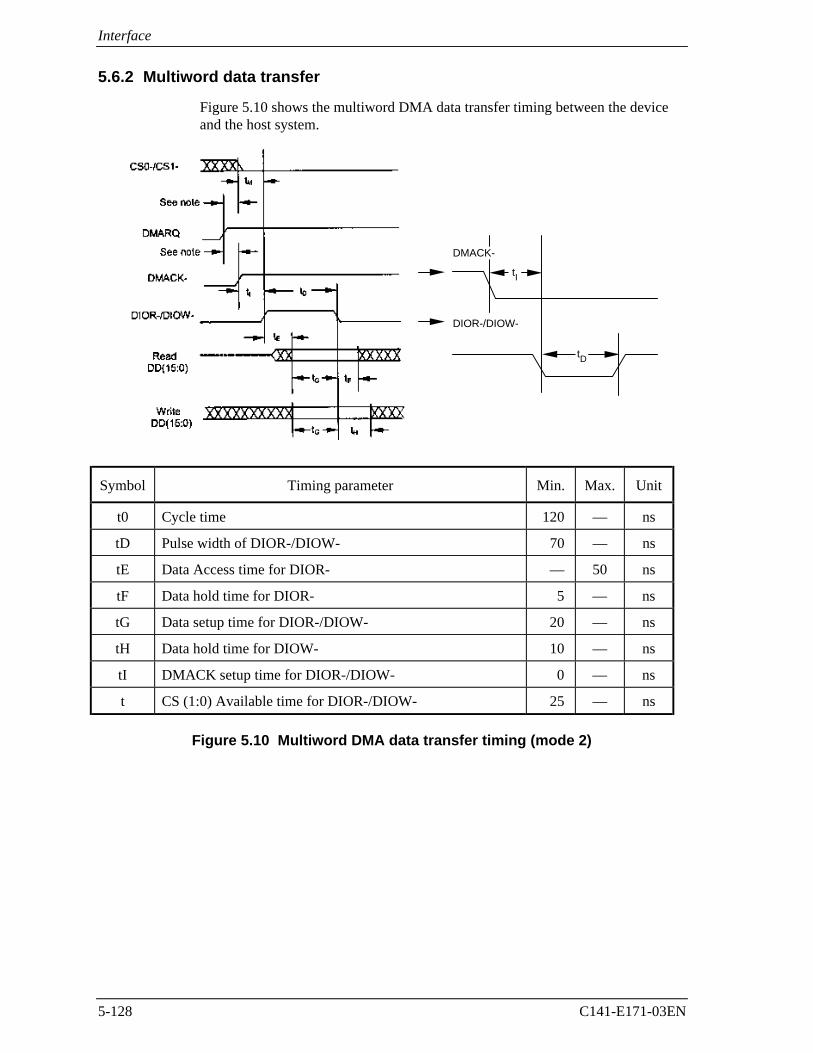
Interface
5-128 C141-E171-03EN
5.6.2 Multiword data transfer
Figure 5.10 shows the multiword DMA data transfer timing between the deviceand the host system.
DMACK-
tD
DIOR-/DIOW-
tI
Symbol Timing parameter Min. Max. Unit
t0 Cycle time 120 — ns
tD Pulse width of DIOR-/DIOW- 70 — ns
tE Data Access time for DIOR- — 50 ns
tF Data hold time for DIOR- 5 — ns
tG Data setup time for DIOR-/DIOW- 20 — ns
tH Data hold time for DIOW- 10 — ns
tI DMACK setup time for DIOR-/DIOW- 0 — ns
t CS (1:0) Available time for DIOR-/DIOW- 25 — ns
Figure 5.10 Multiword DMA data transfer timing (mode 2)

5.5 Ultra DMA Feature Set
C141-E171-03EN 5-129
5.6.3 Ultra DMA data transfer
Figures 5.11 through 5.20 define the timings associated with all phases of UltraDMA bursts.
Table 5.18 contains the values for the timings for each of the Ultra DMA Modes.
5.6.3.1 Initiating an Ultra DMA data in burst
5.6.3.2 contains the values for the timings for each of the Ultra DMA Modes.
Note:
The definitions for the STOP, HDMARDY-and DSTROBE signal lines arenot in effect until DMARQ and DMACK- are asserted.
Figure 5.11 Initiating an Ultra DMA data in burst
DMARQ(device)
DMACK- (host)
STOP(host)
HDMARDY- (host)
DSTROBE (device)
DD (15:0)
DA0,DA1,DA2, CS0-,CS1-
tUI
tENV
tFS
tENV
tZAD
tFS
tZAD
tDVHtAZ
tZIORDY
tACK
tACK
tACK
tVDS
tDZFS
tZFS

Interface
5-130 C141-E171-03EN
5.6.3.2 Ultra DMA data burst timing requirements
Table 5.18 Ultra DMA data burst timing requirements (1 of 2)
NAME MODE 0(in ns)
MODE 1(in ns)
MODE 2(in ns)
MODE 3(in ns)
MODE 4(in ns)
MODE 5(in ns)
COMMENT
MIN MAX MIN MAX MIN MAX MIN MAX MIN MAX MIN MAX
t2CYCTYP240 160 120 90 60 40 Typical sustained average two
cycle time
tCYC112 73 54 39 25 16.8 Cycle time allowing for
asymmetry and clock variations(from STROBE edge to STROBEedge)
t2CYC230 153 115 86 57 38 Two cycle time allowing for
clock variations (from rising edgeto next rising edge or from fallingedge to next falling edge ofSTROBE)
tDS15 10 7 7 5 4 Data setup time at recipient (from
data valid until STROBE edge)(*2), (*5)
tDH5 5 5 5 5 4.6 Data hold time at recipient (from
STROBE edge until data maybecome invalid) (*2), (*5)
tDVS70 48 31 20 6.7 4.8 Data valid setup time at sender
(from data valid until STROBEedge) (*3)
tDVH6.2 6.2 6.2 6.2 6.2 4.8 Data valid hold time at sender
(from STROBE edge until datamay become invalid) (*3)
tCS15 10 7 7 5 5 CRC word setup time at device
(*2)
tCH5 5 5 5 5 5 CRC word hold time device (*2)
tCVS70 48 31 20 6.7 10 CRC word valid setup time at
host (from CRC valid untilDMACK-negation) (*3)
tCVH6.2 6.2 6.2 6.2 6.2 10 CRC word valid hold time at
sender (from DMACK-negationuntil CRC may become invalid)(*3)
tZFS0 0 0 0 0 35 Time from STROBE output
released-to-driving until the firsttransition of critical timing
tDZFS70 48 31 20 6.7 25 Time from data output released-
to-driving until the first transitionof critical timing
tFS230 200 170 130 120 90 First STROBE time (for device to
first negate DSTROBE fromSTOP during a data in burst)

5.5 Ultra DMA Feature Set
C141-E171-03EN 5-131
Table 5.18 Ultra DMA data burst timing requirements (2 of 2)
MODE 0(in ns)
MODE 1(in ns)
MODE 2(in ns)
MODE 3(in ns)
MODE 4(in ns)
MODE 5(in ns)
NAME
MIN MAX MIN MAX MIN MAX MIN MAX MIN MAX MIN MAX
COMMENT
tLI0 150 0 150 0 150 0 100 0 100 0 75 Limited interlock time (*1)
tMLI20 20 20 20 20 20 Interlock time with minimum (*1)
TUI0 0 0 0 0 0 Unlimited interlock time (*1)
tAZ 10 10 10 10 10 10 Maximum time allowed for outputdrivers to release (from asserted ornegated)
tZAH 20 20 20 20 20 20 Minimum delay time required foroutput
tZAD 0 0 0 0 0 0 Drivers to assert or negate (fromreleased)
tENV 20 70 20 70 20 70 20 55 20 55 20 50 Envelope time (from DMACK- toSTOP and HDMARDY- duringdata in burst initiation and fromDMACK to STOP during data outburst initiation)
tRFS 75 70 60 60 60 50 Ready-to-final-STROBE time (noSTROBE edges shall be sent thislong after negation of DMARDY-)
tRP 160 125 100 100 100 85 Ready-to-pause time (thatrecipient shall wait to pause afternegating DMARDY-)
tIORDYZ 20 20 20 20 20 20 Maximum time before releasingIORDY
tZIORDY 0 0 0 0 0 0 Minimum time before drivingIORDY (*4)
tACK 20 20 20 20 20 20 Setup and hold times forDMACK- (before assertion ornegation)
tSS 50 50 50 50 50 50 Time from STROBE edge tonegation of DMARQ or assertionof STOP (when sender terminatesa burst)
*1: Except for some instances of tMLI that apply to host signals only, the parameters tUI, tMLI and tLI indicate sender-to-recipient or recipient-to-sender interlocks, i.e., one agent (either sender or recipient) is waiting for the other agent to respond with a signal beforeproceeding. tUI is an unlimited interlock that has no maximum time value. tMLI is a limited time-out that has a defined minimum. tLI
is a limited time-out that has a defined maximum.
*2: 80-conductor cabling shall be required in order to meet setup (tDS, tCS) and hold (tDH, tCH) times in modes greater than 2.*3: Timing for tDVS, tDVH, tCVS and tCVH shall be met for lumped capacitive loads of 15 and 40 pf at the connector where all signals (Data and
STROBE) have the same capacitive load value. Due to reflections on the cable, the measurement of these timings is not valid in anormally functioning system.
*4: For all modes the parameter tZIORDY may be greater than tENV due to the fact that the host has a pull up on IORDY- giving it a knownstate when not actively driven.
*5: The parameters tDS, and tDH for mode 5 is defined for a recipient at the end of the cable only in a configuration with one device at theend of the cable.
Note: All timing measurement switching points (low to high and high to low) shall be taken at 1.5V.

Interface
5-132 C141-E171-03EN
Table 5.19 Ultra DMA sender and recipient timing requirements
MODE 0(in ns)
MODE 1(in ns)
MODE 2(in ns)
MODE 3(in ns)
MODE 4(in ns)
MODE 5(in ns)
NAMEMIN MAX MIN MAX MIN MAX MIN MAX MIN MAX MIN MAX
COMMENT
tDSIC 14.7 9.7 6.8 6.8 4.8 2.3 Recipient IC data setup time (fromdata valid until STROBE edge)(*1)
tDHIC 4.8 4.8 4.8 4.8 4.8 2.8 Recipient IC data hold time (fromSTROBE edge until data maybecome invalid) (*1)
tDVSIC 72.9 50.9 33.9 22.6 9.5 6 Sender IC data valid setup time(from data valid until STROBEedge) (*2)
tDVHIC 9 9 9 9 9 6 Sender IC data valid hold time(from STROBE edge until datamay become invalid) (*2)
*1: The correct data value shall be captured by the recipient given input data with a slew rate of 0.4 V/ns rising and falling and the inputSTROBE with a slew rate of 0.4 V/ns rising and falling at tDSIC and tDHIC timing (as measured through 1.5V).
*2: The parameters tDVSIC and tDVHIC shall be met for lumped capacitive loads of 15 and 40 pf at the IC where all signals have the samecapacitive load value. Noise that may couple onto the output signals from external sources in a normally functioning system has notbeen included in these values.
Note:
All timing measurement switching points (low to high and high to low) shall be taken at 1.5V.

5.5 Ultra DMA Feature Set
C141-E171-03EN 5-133
5.6.3.3 Sustained Ultra DMA data in burst
5.6.3.2 contains the values for the timings for each of the Ultra DMA Modes.
Note:
DD (15:0) and DSTROBE signals are shown at both the host and the deviceto emphasize that cable setting time as well as cable propagation delay shallnot allow the data signals to be considered stable at the host until some timeafter they are driven by the device.
Figure 5.12 Sustained Ultra DMA data in burst
DSTROBEat device
DD(15:0)at device
DSTROBEat host
DD(15:0)at host
t2CYC
tCYC
tDVStDVSIC
tDVHtDVHIC
tDStDSIC
tDHtDHIC
t2CYC
tCYC
tDVStDVSIC
tDVHtDVHIC
tDHtDHIC
tDHtDHIC
tDVHtDVHIC
tDStDSIC

Interface
5-134 C141-E171-03EN
5.6.3.4 Host pausing an Ultra DMA data in burst
5.6.3.2 contains the values for the timings for each of the Ultra DMA Modes.
Notes:
1) The host may assert STOP to request termination of the Ultra DMA burstno sooner than tRP after HDMARDY- is negated.
2) After negating HDMARDY-, the host may receive zero, one, two or threemore data words from the device.
Figure 5.13 Host pausing an Ultra DMA data in burst
tRP
tRFS
DMARQ(device)
DMACK- (host)
STOP(host)
HDMARDY- (host)
DSTROBE (device)
DD(15:0) (device)

5.5 Ultra DMA Feature Set
C141-E171-03EN 5-135
5.6.3.5 Device terminating an Ultra DMA data in burst
5.6.3.2 contains the values for the timings for each of the Ultra DMA Modes.
Note:
The definitions for the STOP, HDMARDY- and DSTROBE signal lines areno longer in effect after DMARQ and DMACK- are negated.
Figure 5.14 Device terminating an Ultra DMA data in burst
DMARQ(device)
DMACK- (host)
DD(15:0)
HDMARDY- (host)
DSTROBE (device)
STOP(host)
DA0, DA1, DA2, CS0-, CS1-
tMLI
tLI tLI
tLI
tACK
tACK
tIORDYZtSS
tZAH
tAZ tCVS tCVH
CRC
tACK

Interface
5-136 C141-E171-03EN
5.6.3.6 Host terminating an Ultra DMA data in burst
5.6.3.2 contains the values for the timings for each of the Ultra DMA Modes.
Note:
The definitions for the STOP, HDMARDY- and DSTROBE signal lines areno longer in effect after DMARQ and DMACK- are negated.
Figure 5.15 Host terminating an Ultra DMA data in burst
DMARQ(device)
tLI tMLI
tRP
tZAHtAZ
tRFStLI
tMLI
tCVS tCVH
tACK
tACK
tACK
tIORDYZ
CRC
DA0, DA1, DA2,CS0, CS1
DMACK-(host)
STOP(host)
HDMARDY- (host)
DSTROBE (device)
DD(15:0)

5.5 Ultra DMA Feature Set
C141-E171-03EN 5-137
5.6.3.7 Initiating an Ultra DMA data out burst
5.6.3.2 contains the values for the timings for each of the Ultra DMA Modes.
Note:
The definitions for the STOP, DDMARDY- and HSTROBE signal lines arenot in effect until DMARQ and DMACK- are asserted.
Figure 5.16 Initiating an Ultra DMA data out burst
DMARQ(device)
DMACK- (host)
STOP(host)
DDMARDY- (device)
HSTROBE (host)
DD(15:0) (host)
DA0, DA1, DA2CS0-, CS1-
tUI
tACKtENV
tZIORDYtUItLI
tACK
tACK
tDVHtDVS
tDZFS

Interface
5-138 C141-E171-03EN
5.6.3.8 Sustained Ultra DMA data out burst
5.6.3.2 contains the values for the timings for each of the Ultra DMA Modes.
Note:
DD (15:0) and HSTROBE signals are shown at both the device and the hostto emphasize that cable setting time as well as cable propagation delay shallnot allow the data signals to be considered stable at the device until sometime after they are driven by the host.
Figure 5.17 Sustained Ultra DMA data out burst
HSTROBEat host
HSTROBEat device
DD(15:0) at host
DD(15:0)at device
t2CYC
tCYC tCYC
t2CYC
tDVHtDVHIC
tDVStDVSIC
tDVStDVSIC
tDVHtDVHIC
tDHtDHIC
tDStDSIC
tDHtDHIC
tDStDSIC
tDHtDHIC
tDVHtDVHIC

5.5 Ultra DMA Feature Set
C141-E171-03EN 5-139
5.6.3.9 Device pausing an Ultra DMA data out burst
5.6.3.2 contains the values for the timings for each of the Ultra DMA Modes.
Notes:
1) The device may negate DMARQ to request termination of the Ultra DMAburst no sooner than tRP after DDMARDY- is negated.
2) After negating DDMARDY-, the device may receive zero, one two or threemore data words from the host.
Figure 5.18 Device pausing an Ultra DMA data out burst
DMARQ(device)
DMACK- (host)
STOP(host)
DDMARDY-(device)
HSTROBE (host)
DD(15:0) (host)
tRP
tRFS

Interface
5-140 C141-E171-03EN
5.6.3.10 Host terminating an Ultra DMA data out burst
5.6.3.2 contains the values for the timings for each of the Ultra DMA Modes.
Note:
The definitions for the STOP, DDMARDY- and HSTROBE signal lines areno longer in effect after DMARQ and DMACK- are negated.
Figure 5.19 Host terminating an Ultra DMA data out burst
DMARQ(device)
DMACK- (host)
STOP(host)
DDMARDY- (device)
HSTROBE (host)
DD(15:0)(host)
tLI
tLI
tSS
tLI
tMLI
tACK
tIORDYZ
tACK
tACK
tCVHtCVS
CRC
DA0, DA1, DA2CS0-, CS1-

5.5 Ultra DMA Feature Set
C141-E171-03EN 5-141
5.6.3.11 Device terminating an Ultra DMA data out burst
5.6.3.2 contains the values for the timings for each of the Ultra DMA Modes.
Note:
The definitions for the STOP, DDMARDY- and HSTROBE signal lines areno longer in effect after DMARQ and DMACK- are negated.
Figure 5.20 Device terminating an Ultra DMA data out burst
DMARQ(device)
DMACK- (host)
STOP(host)
DDMARDY- (device)
HSTROBE (host)
DD(15:0) (host)
DA0, DA1, DA2, CS0-, CS1-
tLI
tLI
tRP
tRFS tMLI
tMLI
tCVS tCVH
tIORDYZ
tACK
tACK
tACK
CRC

Interface
5-142 C141-E171-03EN
5.6.4 Power-on and reset
Figure 5.21 shows power-on and reset (hardware and software reset) timing.
(1) Only master device is present
*1: Reset means including Power-on-Reset, Hardware Reset (RESET-), and Software Reset.
Clear Reset *1
tP
tN
tM
BSY
DASP-
Power-onRESET-Software reset
(2) Master and slave devices are present (2-drives configuration)
tP
Clear Reset
[Slave device]
[Master device] tN
DASP-
PDIAG-
BSY
BSY
DASP-
tQ
tR
tS
Symbol Timing parameter Min. Max. Unit
tM Pulse width of RESET- 25 — µs
tN Time from RESET- negation to BSY set — 400 ns
tP Time from RESET- negation to DASP- or DIAG- negation — 1 ms
tQ Self-diagnostics execution time — 30 s
tR Time from RESET- negation to DASP- assertion (slavedevice)
— 400 ms
tS Duration of DASP- assertion — 31 s
Figure 5.21 Power-on Reset Timing

C141-E171-03EN 6-1
CHAPTER 6 Operations
6.1 Device Response to the Reset
6.2 Power Save
6.3 Defect Processing
6.4 Read-Ahead Cache
6.5 Write Cache

Operations
6-2 C141-E171-03EN
6.1 Device Response to the Reset
This section describes how the PDIAG- and DASP- signals responds when thepower of the IDD is turned on or the IDD receives a reset or diagnostic command.
6.1.1 Response to power-on
After the master device (device 0) releases its own power-on reset state, themaster device shall check a DASP- signal for up to 450 ms to confirm presence ofa slave device (device 1). The master device recognizes presence of the slavedevice when it confirms assertion of the DASP- signal. Then, the master devicechecks a PDIAG- signal to see if the slave device has successfully completed thepower-on diagnostics.
If the master device cannot confirm assertion of the DASP- signal within 450 ms,the master device recognizes that no slave device is connected.
After the slave device (device 1) releases its own power-on reset state, the slavedevice shall report its presence and the result of power-on diagnostics to themaster device as described below:
DASP- signal: Asserted within 400 ms.
PDIAG- signal: Negated within 1 ms and asserted within 30 seconds.
The asserted PDIAG-signal is negated 30 seconds after it is asserted if thecommand is not received.

6.1 Device Response to the Reset
C141-E171-03EN 6-3
Max. 31 sec.
Max. 400 ms.
Max. 30 sec.
Max. 1 ms.
If presence of a slave device isconfirmed, PDIAG- is checked forup to 31 seconds.
Checks DASP- for up to450 ms.
DASP-
PDIAG-
BSY bit
Power On Reset-
Status Reg.BSY bit
Power On Reset-
Slave device
Master device
Power on
Figure 6.1 Response to power-on
Note: Figure 6.1 has a assumption that the device is kept on the power-off condition for more than5 sec before the device power is turned on.
6.1.2 Response to hardware reset
Response to RESET- (hardware reset through the interface) is similar to thepower-on reset.
Upon receipt of hardware reset, the master device checks a DASP- signal for upto 450 ms to confirm presence of a slave device. The master device recognizes thepresence of the slave device when it confirms assertion of the DASP- signal.Then the master device checks a PDIAG- signal to see if the slave device hassuccessfully completed the self-diagnostics.
If the master device cannot confirm assertion of the DASP- signal within 450 ms,the master device recognizes that no slave device is connected.

Operations
6-4 C141-E171-03EN
After the slave device receives the hardware reset, the slave device shall report itspresence and the result of the self-diagnostics to the master device as describedbelow:
DASP- signal: Asserted within 400 ms.
PDIAG- signal: Negated within 1 ms and asserted within 30 seconds.
The asserted PDIAG-signal is negated 30 seconds after it is asserted if thecommand is not received.
.
Max. 31 sec.
Max. 400 ms.
Max. 30 sec.
Max. 1 ms.
If presence of a slave device isconfirmed, PDIAG- is checked forup to 31 seconds.
Checks DASP- for up to450 ms.
DASP-
PDIAG-
BSY bit
Reset-
Status Reg.BSY bit
Slave device
Master device
Figure 6.2 Response to hardware reset
Note: Master Device does not check the DASP signal assertion for 2ms upon receipt of hardwarereset.

6.1 Device Response to the Reset
C141-E171-03EN 6-5
6.1.3 Response to software reset
The master device does not check the DASP- signal for a software reset. If aslave device is present, the master device checks the PDIAG- signal for up to 15seconds to see if the slave device has completed the self-diagnosis successfully.
After the slave device receives the software reset, the slave device shall report itspresence and the result of the self-diagnostics to the master device as describedbelow:
PDIAG- signal: negated within 1 ms and asserted within 30 seconds
The asserted PDIAG-signal is negated 30 seconds after it is asserted if thecommand is not received.
When the IDD is set to a slave device, the IDD asserts the DASP- signal whennegating the PDIAG- signal.
Max. 31 sec.
Max. 30 sec.
Max. 1 ms.
If the slave device is preset, PDIAG- is checked forup to 31 seconds.
DASP-
PDIAG-
BSY bit
X"00"X'3F6' Reg.
X"0C"or X"04"
Status Reg.BSY bit
Slave device
Master device
Figure 6.3 Response to software reset

Operations
6-6 C141-E171-03EN
6.1.4 Response to diagnostic command
When the master device receives an EXECUTE DEVICE DIAGNOSTICcommand and the slave device is present, the master device checks the PDIAG-signal for up to 6 seconds to see if the slave device has completed the self-diagnosis successfully.
The master device does not check the DASP- signal.
After the slave device receives the EXECUTE DEVICE DIAGNOSTICcommand, it shall report the result of the self-diagnostics to the master device asdescribed below:
PDIAG- signal: negated within 1 ms and asserted within 5 seconds
The asserted PDIAG-signal is negated 5 seconds after it is asserted if thecommand is not received. If the command is received, the PDIAG-signal isnegated according to timing at which the command is received.
When the IDD is set to a slave device, the IDD asserts the DASP- signal whennegating the PDIAG- signal.
Max. 6 sec.
Max. 5 sec.
Max. 1 ms.
If the slave device is preset, PDIAG- signal is checked forup to6 seconds.
DASP-
PDIAG-
BSY bit
X'1F7' Reg.Write
Status Reg.BSY bit
Slave device
Master device
Figure 6.4 Response to diagnostic command

6.2 Power Save
C141-E171-03EN 6-7
6.2 Power Save
The host can change the power consumption state of the device by issuing apower command to the device.
6.2.1 Power save mode
There are five types of power consumption state of the device including activemode where all circuits are active.
• Active mode
• Active idle mode
• Low power idle mode
• Standby mode
• Sleep mode
The device enters the active idle mode by itself. The device also enters the idlemode in the same way after power-on sequence is completed. The subsequentmode transition changes depending on the APM setting.
(1) Active mode
In this mode, all the electric circuit in the device are active or the device is underseek, read or write operation.
A device enters the active mode under the following conditions:
• The media access system is received.
(2) Active idle mode
In this mode, circuits on the device is set to power save mode.
The device enters the Active idle mode under the following conditions:
• After completion of the command execution other than SLEEP and STANDBYcommands.
(3) Low power idle mode
Sets circuits on the device to the power save mode. The heads are disabled in thesafe state.
The device enters the low power mode under the following conditions:
• After certain amount of time has elapsed in the active idle state (APM Mode1 and Mode 2)
• Upon completion of the power-on sequence

Operations
6-8 C141-E171-03EN
• Upon receipt of a hard reset
• Upon receipt of Idle/Idle Intermediate
(4) Standby mode
In this mode, the spindle motor has stopped from the low power idle state.
The device can receive commands through the interface. However if a commandwith disk access is issued, response time to the command under the standby modetakes longer than the active, active idle, or low power idle mode because theaccess to the disk medium cannot be made immediately.
The drive enters the standby mode under the following conditions:
• A STANDBY or STANDBY IMMEDIATE command is issued.
• A certain amount of time has elapsed in the low power idle state. (APMMode 2)
• The time specified by the STANDBY or IDLE command has elapsed aftercompletion of the command.
• A reset is issued in the sleep mode.
When one of following commands is issued, the command is executed normallyand the device is still stayed in the standby mode.
• Reset (hardware or software)
• STANDBY command
• STANDBY IMMEDIATE command
• INITIALIZE DEVICE PARAMETERS command
• CHECK POWER MODE command
(5) Sleep mode
The power consumption of the drive is minimal in this mode. The drive entersonly the standby mode from the sleep mode. The only method to return from thestandby mode is to execute a software or hardware reset.
The drive enters the sleep mode under the following condition:
• A SLEEP command is issued.
In this mode, the device does not accept the command. (It is ignored.)

6.3 Defect Processing
C141-E171-03EN 6-9
6.2.2 Power commands
The following commands are available as power commands.
• IDLE
• IDLE IMMEDIATE
• STANDBY
• STANDBY IMMEDIATE
• SLEEP
• CHECK POWER MODE
• SET FEATURES (APM setting)
6.3 Defect Processing
This device performs alternating processing where the defective sector isalternated with the spare area depending on media defect location information.The media defect location information is registered in the system space specifiedfor the user area according to the format at shipment of the media from the plant.
6.3.1 Spare area
The following two types of areas are prepared as the spare area in user areas:
1) Spare area for sector slip: At shipment of the media from the plant, this areais defined for use in alternating processing for defective sectors during formatprocessing. 254 sectors/128 tracks.
2) Spare cylinder for alternate assignment: This cylinder is used duringautomatic alternating processing for defective sector. 2000 sectors/drive.
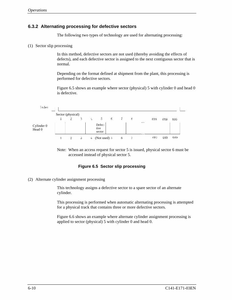
Operations
6-10 C141-E171-03EN
6.3.2 Alternating processing for defective sectors
The following two types of technology are used for alternating processing:
(1) Sector slip processing
In this method, defective sectors are not used (thereby avoiding the effects ofdefects), and each defective sector is assigned to the next contiguous sector that isnormal.
Depending on the format defined at shipment from the plant, this processing isperformed for defective sectors.
Figure 6.5 shows an example where sector (physical) 5 with cylinder 0 and head 0is defective.
Sector (physical)
Cylinder 0Head 0
Defec-tivesector
(Not used)
Note: When an access request for sector 5 is issued, physical sector 6 must beaccessed instead of physical sector 5.
Figure 6.5 Sector slip processing
(2) Alternate cylinder assignment processing
This technology assigns a defective sector to a spare sector of an alternatecylinder.
This processing is performed when automatic alternating processing is attemptedfor a physical track that contains three or more defective sectors.
Figure 6.6 shows an example where alternate cylinder assignment processing isapplied to sector (physical) 5 with cylinder 0 and head 0.

6.3 Defect Processing
C141-E171-03EN 6-11
Sector (physical)
Cylinder 0Head 0
Defec-tivesector
(Not used)
Alternate cylinder 0Head 0
This is assigned to an unassigned sector.Alreadyassigned
Notes:
1. The alternate cylinder is assigned to an inner cylinder in each zone.
2. When an access request for sector 5 is issued, the sector assigned foralternating processing of the alternate cylinder must be accessed instead ofphysical sector 5.
If an access request for sectors after sector 5 is issued, seek is executed tocylinder 0, head 0 in order to continue processing.
Figure 6.6 Alternate cylinder assignment processing
(3) Automatic alternating processing
This device performs automatic alternating processing in the event of any of thefollowing errors.
• Automatic alternating processing is attempted for read error recovery byheightening the ECC correction capability while a read error retry is inprogress.
Before attempting automatic alternating processing, writing and reading ofalready corrected data is repeated for the sector in which an error occurred.If a read error does not occur during this reading operation, automaticalternating processing is not performed.
• If error recovery is not successful even if a write fault error retry is executed,automatic alternating processing is performed.

Operations
6-12 C141-E171-03EN
6.4 Read-ahead Cache
Read-ahead Cache is the function for automatically reading data blocks uponcompletion of the read command in order to read data from disk media and savedata block on a data buffer.
If a subsequent command requests reading of the read-ahead data, data on the databuffer can be transferred without accessing the disk media. As the result, fasterdata access becomes possible for the host.
6.4.1 Data buffer structure
This device contains a data buffer of 2 MB. This buffer is divided into two areas:one area is used for MPU work, and the other is used as a read cache for anothercommand. (See Figure 6.7.)
For MPU work For R/W command
2048 KB (2097152 bytes)
0.5 KB(512 bytes)
1984 KB(2031616 bytes)
63.5 KB(65024 bytes)
For MPU work
Figure 6.7 Data buffer structure
The read-ahead operation is performed while the READ SECTOR (S) or READMULTIPLE or READ DMA command is in progress. Read-ahead data is storedin the read cache part of the buffer.
6.4.2 Caching operation
The caching operation is performed only when the commands listed below arereceived. If any of the following data are stored on the data buffer, the data issent to the host system.
• All of the sector data that this command processes.
• A part of the sector data including the start sector, that this commandprocesses.
If part of the data to be processed is stored on the data buffer, the remaining datais read from disk media and sent to the host system.

6.4 Read-ahead Cache
C141-E171-03EN 6-13
(1) Commands that are targets of caching
The commands that are targets of caching are as follows:
• READ SECTOR(S (EXT)
• READ MULTIPLE (EXT)
• READ DMA (EXT)
However, if the caching function is prohibited by the SET FEATURES command,the caching operation is not performed.
(2) Data that is a target of caching
The data that is a target of caching are as follows:
1) Read-ahead data that is read from disk media and saved to the data bufferupon completion of execution of a command that is a target of caching.
2) Data required by a command that is a target of caching and has been sent tothe host system once. If the sector data requested by the host has not beencompletely stored in the read cache portion of the buffer, this data does notbecome a target of caching. Also, if sequential hits occur continuously, thecaching-target data required by the host becomes invalid.
(3) Invalidating caching-target data
Data that is a target of caching on the data buffer is invalidated under thefollowing conditions:
1)-1Any command other than the following commands is issued. (All caching-target data is invalidated.)
WRITE VERIFY
WRITE LONG
READ BUFFER
FORMAT TRACK
IDENTIFY COMPONENT
SECURITY ERASE UNIT
STANDBY
STANDBY IMMEDIATE
UNSUPPORT COMMAND (INVALID COMMAND)

Operations
6-14 C141-E171-03EN
1)-2Commands that partially invalidate caching data
(When data in the buffer or on media is overwritten, the overwritten data isinvalidated.)
READ DMA / READ MULTIPLE / READ SECTOR (S)
READ DMA EXT / READ MULTIPLE EXT / READ SECTOR (S) EXT
WRITE DMA / WRITE MULTIPLE / WRITE SECTOR (S)
WRITE DMA EXT / WRITE MULTIPLE EXT / WRITE SECTOR (S) EXT
SET MAX ADDRESS
SECURITY SET PASSWORD
SECURITY UNLOCK
SECURITY ERASE UNIT
SECURITY DISABLE PASSWORD
DEVICE CONFIGURATION IDENTITY
DEVICE CONFIGURATION SET
2) The caching operation is invalidated by the SET FEATURES command.
3) A soft/hard reset is issued or the power is turned off.
4) When a shift is made to the power saving mode at the Low Power Idle levelor lower.
5) When the above commands are aborted.
READ DMA / READ MULTIPLE / READ SECTOR (S)READ DMA EXT / READ MULTIPLE EXT / READ SECTOR (S) EXTWRITE DMA / WRITE MULTIPLE EXT / WRITE SECTOR (S)WRITE DMA EXT / WRITE MULTIPLE EXT / WRITE SECTOR (S) EXT
6) When HOST CRC ERROR has occurred.

6.4 Read-ahead Cache
C141-E171-03EN 6-15
6.4.3 Using the read segment buffer
Methods of using the read segment buffer are explained for the followingsituations.
6.4.3.1 Miss-hit (no hit)
In this situations, the top block of read requested data is not stored at all in thedata buffer. As a result, all of the read requested data is read from disk media.
1) HAP (host address point) and DAP (disk address point) are defined in thesequential address of the segment that is read last.
Read segment
DAP (disk address pointer)
HAP (host address pointer)
2) During reading of read requested data, the request data that has already beenread is sent to the host system.
Read requested data
Read requested data isstored until this point.
Free space
DAP
HAP
3) When reading of read requested data is completed and transfer of the readrequested data to the host system is completed, reading of the disk continuesuntil a certain amount of data is stored.
Read requested data Read-ahead data
DAP
(stop)HAP
(stop)

Operations
6-16 C141-E171-03EN
4) The following cache valid data is for the read command that is executed next:
START LBA(Logical block address)
Cache valid data
LAST LBA
6.4.3.2 Sequential reading
The read-ahead operation is performed for the read buffer when the readcommand that is targeted at a sequential address is received after execution of theread command is completed.
1. Sequential command immediately after non-sequential command
1) When the sequential read command is received, DAP and HAP are set in thesequential address of the last read command, and read requested data is read.
Free spaceHit error data
DAP
HAP
2) During reading of read requested data, the request data that has already beenread is sent to the host system.
Read requested dataHit error data Free space
HAP
DAP
3) When reading of read requested data is completed and transfer of the readrequested data to the host system is completed, the read-ahead operationcontinues until a certain amount of data is stored.
Hit error data Read requested data
HAP
DAP
Read-ahead data Free space

6.4 Read-ahead Cache
C141-E171-03EN 6-17
b. Sequential hit
When the end sector address of the read command received the last time and thetop sector address of the read command this time are consecutive, hit data alreadystored on the buffer is transferred to the host system.
At the same time as a transfer of the hit data to the host system starts, the newread-ahead operation for the subsequent data is implemented in the free space thathas been made available by the data transfer.
1) The following state is established when the read command is received.
START LBALAST LBADAP
HAP (being consecutive after the last set of read requested data)
Hit dataRead-ahead data
2) At the same time as a transfer of hit data starts, reading of read-ahead data isstarted for as many spaces as are made available by the transfer.
DAP
HAP
Hit dataNew read-ahead dataRead-ahead data
3) When transfer of the hit data is complete, the read-ahead operation isperformed as many times as required for the amount of transferred hit data.
Read-ahead data
HAP
DAP

Operations
6-18 C141-E171-03EN
6.4.3.3 Full hit
In this situation, all read requested data is stored in the data buffer. Transfer ofthe read requested data is started from the location where hit data is stored. Fordata that is a target of caching and remains before a full hit, the data is retainedwhen execution of the command is completed. This is done so that a new read-ahead operation is not performed. If the full hit command is received during theread-ahead operation, a transfer of the read requested data starts while the read-ahead operation is in progress.
1) An example is the state shown below where the previous read command isexecuting sequential reading. First, HAP is set at the location where hit datais stored.
HAP (It is reset to the hit data location for transfers.)
HAP end location of the previous read command
DAP end location of the previous read command
Cache dataFull hit dataCache data
HAP
DAP
2) The read requested data is transferred, and a new read-ahead operation is notperformed.
(stop)HAP
Cache dataFull hit dataCache data

6.4 Read-ahead Cache
C141-E171-03EN 6-19
6.4.3.4 Partial hit
In this situation, a part of read requested data including the top sector is stored inthe data buffer. A transfer of the read requested data starts from the addresswhere the data that is hit is stored until the top sector of the read requested data.Remaining part of insufficient data is read then.
An example is a case where a partial hit occurs in cache data, as shown below.
LAST LBA
Cache valid data
START LBA
1) HAP is set at the address where partial hit data is stored. DAP is then set tothe address immediately after the partial hit data.
HAP
DAP
Partial hit data Insufficient data
2) At the same time as a transfer of the partial hit data starts, insufficient data isread.
(stop)HAP
Read requested data to be transferred
DAP
Partial hit data Insufficient data

Operations
6-20 C141-E171-03EN
6.5 Write Cache
Write Cache is the function for reducing the command processing time byseparating command control to disk media from write control to disk media.When Write Cache is permitted, the write command can be keep receiving as longas the space available for data transfers remains free on the data buffer. Becauseof this function, command processing appears to be completed swiftly from theviewpoint of the host. It improves system throughput.
6.5.1 Caching operation
(1) Commands that are targets of caching
The commands that are targets of caching are as follows:
• WRITE SECTOR (S)
• WRITE MULTIPLE
• WRITE DMA
• WRITE SECTOR (S) EXT
• WRITE MULTIPLE EXT
• WRITE DMA EXT
However, the caching operation is not performed when the caching function isprohibited by the SET FEATURES command.
(2) Invalidation of cached data
If an error occurs during writing onto media, write processing is repeated up to asmany times as specified for retry processing. If retry fails for a sector because theretry limit is reached, automatic alternate sector processing is executed for thesector. If the automatic alternate sector processing fails, the data in the sector forwhich automatic alternate sector processing failed is invalidated without beingguaranteed.
If data remains in sectors following a sector for which automatic alternate sectorprocessing failed, the data is invalidated without being guaranteed.
<Exception>
• If a reset or command is received while a transfer of one sector of data is inprogress, data is not written in the sector of the media where the interruptionoccurred.

6.5 Write Cache
C141-E171-03EN 6-21
(3) Status report in the event of an error
The status report concerning an error occurring during writing onto media iscreated when the next command is issued. Where the command reporting theerror status is not executed, only the error status is reported. Only the status of anerror that occurs during write processing is reported.
<Exceptions>
The error status is not reported in the following case:
• The reset command is received after an error has occurred during writing tomedia.
• Reset processing is performed as usual. The error status that has occurredduring writing to media is not reported.
(4) Enabling and disabling
Enabling and disabling of the Write Cache function can be set only with the SETFEATURES command. The setting does not changed even when the error statusis reported.
The initial setting is stored in the system area of media. System area informationis loaded whenever the power is turned on.
(5) Reset response
When a reset is received while cached data is stored on the data buffer, data of thedata buffer is written on the media, and reset processing is then performed. Thisis true for both a hard reset and soft reset.
IMPORTANT
If Write Cache is enabled, there is a possibility that data transferredfrom the host with the Write Cache enable command is notcompletely written on disk media before the normal end interrupt isissued.If an unrecoverable error occurs while multiple commands that aretargets of write caching are received, the host has difficultydetermining which command caused the error. (An error report isnot issued to the host if automatic alternating processing for theerror is performed normally.) Therefore, the host cannot execute aretry for the unrecoverable error while Write Cache is enabled. Bevery careful on this point when using this function.If a write error occurs, an abort response is sent to all subsequentcommands.

This page is intentionally left blank.

C141-E171-03EN GL-1
Glossary
Actuator
Head positioning assembly. The actuator consists of a voice coil motor and headarm. If positions the read-write (R-W) head.
AT bus
A bus between the host CPU and adapter board
ATA (AT Attachment) standard
The ATA standard is for a PC AT interface regulated to establish compatibilitybetween products manufactured by different vendors. Interfaces based on thisstandard are called ATA interfaces.
BIOS standard for drives
The BIOS standard collectively refers to the parameters defined by the host,which, for example, include the number of cylinders, the number of heads, andthe number of sectors per track in the drive. The physical specifications of thedrive do not always correspond to these parameters.
The BIOS of a PC AT cannot make full use of the physical specifications of thesedrivers. To make the best use of these drives, a BIOS that can handle the standardparameters of these drives is required.
Command
Commands are instructions to input data to and output data from a drive.Commands are written in command registers.
Data block
A data block is the unit used to transfer data. A data block normally indicates asingle sector.
DE
Disk enclosure. The DE includes the disks, built-in spindle motor, actuator,heads, and air filter. The DE is sealed to protect these components from dust.
Master (Device 0)
The master is the first drive that can operate on the AT bus. The master is daisy-chained with the second drive which can operate in conformity with the ATAstandard.

Glossary
GL-2 C141-E171-03EN
MTBF
Mean time between failures. The MTBF is calculated by dividing the totaloperation time (total power-on time) by the number of failures in the disk driveduring operation.
MTTR
Mean time to repair. The MTTR is the average time required for a service personto diagnose and repair a faulty drive.
PIO (Programmed input-output)
Mode to transfer data under control of the host CPU
Positioning
Sum of the seek time and mean rotational delay
Power save mode
The power save modes are idle mode, standby mode, and sleep mode.
In idle mode, the drive is neither reading, writing, nor seeking data. In standbymode, the spindle motor is stopped and circuits other than the interface controlcircuit are sleeping. The drive enters sleep mode when the host issues the SLEEPcommand.
Reserved
Reserved bits, bytes, and fields are set to zero and unusable because they arereserved for future standards.
Rotational delay
Time delay due to disk rotation. The mean delay is the time required for half adisk rotation. The mean delay is the average time required for a head to reach asector after the head is positioned on a track.
Seek time
The seek time is the time required for a head to move from the current track toanother track. The seek time does not include the mean rotational delay.
Slave (Device 1)
The slave is a second drive that can operate on the AT bus. The slave is daisy-chained with the first drive operating in conformity with the ATA standard.

Glossary
C141-E171-03EN GL-3
Status
The status is a piece of one-byte information posted from the drive to the hostwhen command execution is ended. The status indicates the commandtermination state.
VCM
Voice coil motor. The voice coil motor is excited by one or more magnets. Inthis drive, the VCM is used to position the heads accurately and quickly.

This page is intentionally left blank.

C141-E171-03EN AB-1
Acronyms and Abbreviations
A
ABRT Aborted commandAIC Automatic idle controlAMNF Address mark not foundATA AT attachmentAWG American wire gage
B
BBK Bad block detectedBIOS Basic input-output system
C
CORR Corrected dataCH Cylinder high registerCL Cylinder low registerCM Command registerCSR Current sense registerCSS Current start/stopCY Cylinder register
D
dBA dB A-scale weightingDE Disk enclosureDH Device/head registerDRDY Drive readyDRQ Ddata request bitDSC Drive seek completeDWF Drive write fault
E
ECC Error checking and correctionER Error registerERR Error
F
FR Feature register
H
HA Host adapter
HDD Hard disk drive
I
IDNF ID not foundIRQ14 Interrupt request 14
L
LED Light emitting diode
M
MB Mega-byteMB/S Mega-byte per secondsMPU Micro processor unit
P
PCA Printed circuit assemblyPIO Programmed input-output
R
RLL Run-length-limited
S
SA System areaSC Sector count registerSG Signal groundSN Sector number registerST Status register
T
TPI Track per inchesTRONF Track 0 not foundTyp Typical
U
UNC Uncorrectable ECC error
V
VCM Voice coil motor

This page is intentionally left blank.

C141-E171-03EN IN-1
Index
A
active idle mode 6-7active mode 6-7alternate cylinder assignment processing
6-10alternating processing,
automatic 6-11for defective sector 6-10for defective sector 6-10
area, spare 6-9assignment processing, alternate cylinder
6-10automatic alternating processing 6-11
B
blower 4-3
C
caching operation 6-12, 6-20command, non-sequential 6-16command, sequential 6-16command, target of caching 6-13command that is target of caching 6-13,
6-20
D
data, target of caching 6-13data buffer structure 6-12data that is target of caching 6-13data transfer,
multiword 5-128PIO 5-127Ultra DMA 5-129
defect processing 6-9device pausing Ultra DMA data out burst
5-139device response 6-2
to reset 6-2device terminating Ultra DMA data
in burst 5-135, 5-141out burst 5-141
E
enabling and disabling 6-21
F
fluctuation,current 1-7full hit 6-18
H
hit, full 6-18hit, no 6-15hit, partial 6-19hit, sequential 6-17host pausing Ultra DMA data in burst
5-134host terminating Ultra DMA data
in burst 5-136out burst 5-140
I
initiaitng, Ultra DMA datain burst 5-129out burst 5-137
initiating Ultra DMA datain burst 5-129out burst 5-137
invalidating, caching-target data 6-13invalidating caching-target data 6-13invalidation of cached data 6-20
L
low power idle mode 6-7
M
mean time, mean time between failuresmiss, hit 6-15miss-hit 6-15mode, active 6-7mode, active idle 6-7mode, power save 6-7mode, sleep 6-8mode, standby 6-8multiword data transfer 5-128multiword DMA data transfer timing 5-128
N
no hit 6-14non-sequential command 6-16

Index
IN-2 C141-E171-03EN
O
operation 6-1operation, caching 6-12operation, read-ahead 6-12
P
partial hit 6-19pausing, device Ultra DMA data out burst
5-139pausing, host Ultra DMA data in burst
5-134PIO data transfer 5-127
timing 5-127power commands 6-9power-on 5-142
timing 5-142power save 6-7
mode 6-7processing, defect 6-9processing, sector slip 6-10
R
read-ahead 6-12cache 6-12operation 6-12
READ DMA 6-13reading, sequential 6-16READ MULTIPLE 6-13READ SECTOR(S) 6-13reset 5-142, 6-2reset response 6-21reset timing 5-142resistor, pull-up or pull-down 5-126response, to
diagnostic command 6-6hardware reset 6-3power-on 6-2software reset 6-5
response todiagnostic command 6-6hardware reset 6-3power-on 6-2software reset 6-5
S
sector slip processing 6-10sequential command 6-16sequential hit 6-17sequential reading 6-16sleep mode 6-8spare area 6-9standby mode 6-8
status report in event of error 6-20sustain, Ultra DMA data
in burst 5-133out burst 5-138
sustained Ultra DMA datain burst 5-133out burst 5-138
T
terminating, device Ultra DMA data outburst 5-135, 5-141
terminating, host Ultra DMA datain burst 5-136out burst 5-140
timing, multiword DMA data transfer5-128
timing, PIO data transfer 5-127timing, power-on 5-142timing, reset 5-142timing requirement, Ultra DMA data burst
5-130
U
Ultra DMA data burst timing requirement5-130
Ultra DMA data transfer 5-129Ultra DMA recipient timing requirement
5-132Ultra DMA sender timing requirement
5-132using, read segment buffer 6-15using read segment buffer 6-15
W
write cache 6-19WRITE SECTOR (S) EXT (34H) 5-102
X
X'B1' 5-90

C141-E171-03EN
Comment Form
We would appreciate your comments and suggestions regarding this manual.
Manual code C141-E171-03EN
Manual name MHS2060AT, MHS2040AT MHS2030AT, MHS2020ATDISK DRIVES PRODUCT MANUAL
Please mark each item: E(Excellent), G(Good), F(Fair), P(Poor).
General appearance ( )Technical level ( )Organization ( )Clarity ( )Accuracy ( )
Illustration ( )Glossary ( )Acronyms & Abbreviations ( )Index ( )
Comments & Suggestions
List any errors or suggestions for improvement.
Page Line Contents
Please send this form to the address below. We will use your comments in planning future editions.
Address: Fujitsu Learning Media Limited37-10 Nishikamata 7-chomeOota-kuTokyo 144-0051JAPAN
Fax: 81-3-3730-3702
Organization:
Name:

This page is intentionally left blank.

MHS2060AT, MHS2040AT MHS2030AT, MHS2020AT DISK DRIVESPRODUCT MANUAL
C141-E171-03EN
MHS2060AT, MHS2040AT MHS2030AT, MHS2020AT DISK DRIVESPRODUCT MANUAL
C141-E171-03EN

This page is intentionally left blank

