metamaterials demonstrating focusing and radiation ...1365/fulltext.pdf · metamaterials...
TRANSCRIPT
Metamaterials Demonstrating Focusing
and Radiation Characteristics Applications
A Dissertation Presented
by
Akram Ahmadi
to
The Department of Electrical and Computer Engineering
in partial fulfillment of the requirements for the degree of
Doctor of Philosophy
in the field of
Electrical Engineering
Northeastern University
Boston, Massachusetts
August 2010
Doctoral Committee:
Assistant Professor Hossein Mosallaei, Dissertation Advisor
Professor Anthony Devaney
Professor Carey Rappaport
Assistant Professor Edwin Marengo


Abstract
Metamaterials Demonstrating Focusing and Radiation Characteristics Applications
Akram Ahmadi
Hossein Mosallaei
This dissertation presents theoretical study and numerical evaluation of metama-
terials demonstrating near-field focusing and radiation characteristics. We start with
physical configuration and performance modeling of all-dielectric metamaterials to de-
velop desired (±ε,±µ) by creating electric and magnetic resonant modes. Arraying
these dipole moments can lead to required material properties. Dielectric particles have
the potential to offer both electric and magnetic dipole modes. We examine dielectric
disks and dielectric spheres as the great candidates for establishing the dipole modes
(metamaterial alphabet), and we demonstrate that a structure constructed from unit-
cells of two different spheres (or disks), where one set of them develops electric modes,
and the other set establishes magnetic modes can provide double negative (DNG)
metamaterials. Then some novel applications of metamaterials are investigated. The
concept of high resolution focusing of negative index materials is investigated and their
performance is compared with those for structures made based on the idea of coupled
surface-modes layers. The resonance performance of an electrically small-size radiator
made of Epsilon Negative (ENG) material is studied next. It is demonstrated how
the material polarization can successfully provide resonance radiation at the negative
material constitutive parameters. One of the possible applications of plasmonic ma-
terials is to build antenna devices radiating and receiving electromagnetic energy at
optical frequencies. Design and fabrication of optical antennas with prescribed spatial
patterns is an interesting and challenging task. Based on the concept of scattering
resonance of plasmonic particles, we illustrate the concept of a reflectarray nanoan-
tenna implemented in optics with the use of array of core-shell dielectric-plasmonic
materials, each of them optimized properly to achieve the required phase shift. We
further present several designs of optical nanoantennas arrays composed of parasitic
plasmonic dipoles and loops where they can enhance radiation characteristics and
direct the optical energy successfully.

c©Northeastern University 2010
All Rights Reserved.
i

To my beloved family.
ii

Acknowledgements
I would like to sincerely thank my research advisor Professor Hossein Mosallaei for his
continuous support and encouragement, and for the opportunity he provided for me to
conduct independent research. I would also like to thank my dissertation committee
members, Professor Anthony Devaney, Professor Carey Rappaport, and Professor Ed-
win Marengo for accepting to be on my dissertation committee. My warmest thanks go
to my beloved family for their constant support and endless love. My parents, Soraya
and Asadollah, deserve my deepest appreciation for their selfless support during this
work and in my whole life. I also feel grateful to Professor Mahmoud Shahabadi from
the University of Tehran, who taught me electromagnetics and helped me to continue
my studying and pursue the Ph.D. I would like to thank all the wonderful staff at
the Electrical Engineering Department. In particular my special thanks to Ms. Faith
Crisley, Ms. Sharon Heath, and Ms. Linda Bonda, for their wonderful assistance dur-
ing my graduate studies at Northeastern University. I am indebted to my officemates
and my colleagues at the ECE Department for many interesting discussions and for
providing a stimulating environment. And thanks to all my friends, especially Shirin
and Morteza for their invaluable friendship and support since the very first days I
came to the United States.
iii

Contents
1 Introduction 1
1.1 Background and Motivation . . . . . . . . . . . . . . . . . . . . . . . . 2
1.1.1 Review of Research Efforts on Nearfield Imaging . . . . . . . . . 3
1.1.2 Review of Research Efforts on Antennas . . . . . . . . . . . . . 4
1.2 Dissertation Overview . . . . . . . . . . . . . . . . . . . . . . . . . . . 5
2 All-Dielectric Metamaterials: Design and Development 9
2.1 Introduction . . . . . . . . . . . . . . . . . . . . . . . . . . . . . . . . . 9
2.2 Periodic Photonic Crystals . . . . . . . . . . . . . . . . . . . . . . . . . 12
2.3 Dielectric Disks: Electric and Magnetic Dipole Creation . . . . . . . . . 16
2.4 Metamaterial Realization . . . . . . . . . . . . . . . . . . . . . . . . . . 21
2.5 Optical Metamaterials . . . . . . . . . . . . . . . . . . . . . . . . . . . 29
2.6 Dispersion Diagram Characteristics of Periodic Array of Dielectric Spheres 35
2.7 Conclusions . . . . . . . . . . . . . . . . . . . . . . . . . . . . . . . . . 36
3 Near-Field Focusing 39
3.1 Introduction . . . . . . . . . . . . . . . . . . . . . . . . . . . . . . . . . 39
3.2 Theory and Formulation of Layered Structures . . . . . . . . . . . . . . 41
3.3 Negative Index Material Slab . . . . . . . . . . . . . . . . . . . . . . . 43
3.4 Coupled Surface-Modes Layers . . . . . . . . . . . . . . . . . . . . . . . 46
3.4.1 Analysis of Multiple Thin Film Systems . . . . . . . . . . . . . 48
3.5 FDTD Numerical Analysis of Finite-Size Structure . . . . . . . . . . . 56
3.6 Conclusions . . . . . . . . . . . . . . . . . . . . . . . . . . . . . . . . . 58
4 Ellipsoidal Metamaterial Subwavelength Radiator 60
4.1 Introduction . . . . . . . . . . . . . . . . . . . . . . . . . . . . . . . . . 60
4.2 Resonance Formulation . . . . . . . . . . . . . . . . . . . . . . . . . . . 62
4.3 Calculation of the Lower Bounds on Q . . . . . . . . . . . . . . . . . . 64
4.4 Performance Analysis of ENG Antennas . . . . . . . . . . . . . . . . . 66
iv

4.4.1 Spherical Radiator . . . . . . . . . . . . . . . . . . . . . . . . . 67
4.4.2 Circular Cylindrical Disk Radiator . . . . . . . . . . . . . . . . 69
4.4.3 Circular Cylindrical Rod Radiator . . . . . . . . . . . . . . . . . 73
4.5 MNG Slab Resonance Radiator . . . . . . . . . . . . . . . . . . . . . . 76
4.6 Conclusions . . . . . . . . . . . . . . . . . . . . . . . . . . . . . . . . . 77
5 Optical Reflectarray Nanoantenna 80
5.1 Introduction . . . . . . . . . . . . . . . . . . . . . . . . . . . . . . . . . 80
5.2 Scattering Characteristic of a Core-Shell Nanoparticle . . . . . . . . . . 81
5.3 Optical Reflectarray Nanoantenna . . . . . . . . . . . . . . . . . . . . . 84
5.3.1 Reflection-Phase Synthesis . . . . . . . . . . . . . . . . . . . . . 86
5.3.2 Plasmonic Core-Shells Array Over a Layered Material . . . . . . 87
5.4 Array Design and Scanned-Beam Characteristics . . . . . . . . . . . . . 91
5.5 Conclusions . . . . . . . . . . . . . . . . . . . . . . . . . . . . . . . . . 95
6 Optical Nanoloops Array Antenna 97
6.1 Introduction . . . . . . . . . . . . . . . . . . . . . . . . . . . . . . . . . 97
6.2 Optical Nanodipole Antennas . . . . . . . . . . . . . . . . . . . . . . . 98
6.2.1 Optical Nanodipole Yagi-Uda Antennas . . . . . . . . . . . . . . 100
6.3 Optical Nanoloop Antennas . . . . . . . . . . . . . . . . . . . . . . . . 103
6.3.1 Optical Nanoloops Array Antenna . . . . . . . . . . . . . . . . . 105
6.4 Conclusions . . . . . . . . . . . . . . . . . . . . . . . . . . . . . . . . . 110
7 Conclusions and Recommendations for Future Work 111
7.1 Summary and Contributions . . . . . . . . . . . . . . . . . . . . . . . . 111
7.1.1 Design and Development of All-Dielectric Metamaterials . . . . 111
7.1.2 Novel Applications of Metamaterials . . . . . . . . . . . . . . . 112
7.2 Future Work . . . . . . . . . . . . . . . . . . . . . . . . . . . . . . . . . 113
A Photonic Band Gap Calculations Using FDTD Method 117
Bibliography 122
v

List of Figures
1.1 Material classifications [1]. . . . . . . . . . . . . . . . . . . . . . . . . . 2
2.1 DNG metamaterial constructed from metallic loops and rods: (a) the
geometry, and (b) its equivalent circuit model. . . . . . . . . . . . . . . 10
2.2 Periodic structure of dielectric slabs: (a) the geometry, and (b) its trans-
mission coefficient. . . . . . . . . . . . . . . . . . . . . . . . . . . . . . 13
2.3 Periodic structure of dielectric rods: (a) the geometry, and (b) its trans-
mission coefficient. Note that one layer of dielectric rods does not gen-
erate any band-gap region. . . . . . . . . . . . . . . . . . . . . . . . . . 14
2.4 Near-field patterns for Ez in the x-y plane (one unit cell) for five-layer
rods: (a) before band gap (f1 = 2.80GHz), and (b) after band gap
(f2 = 6.60GHz). Note the confinement of dielectric and air modes
inside the dielectric and air regions, respectively. . . . . . . . . . . . . . 15
2.5 Near-field patterns for Ez in the x-y plane (one unit cell) for one-layer
rods at (a) f1 = 2.80GHz, and (b) f2 = 6.60GHz. . . . . . . . . . . . . 16
2.6 Array of all-dielectric disks: (a) the geometry (Λx = Λy = Λz = 1.5cm),
and transmission coefficients for (b) five-layer structure, and (c) one-
layer structure. . . . . . . . . . . . . . . . . . . . . . . . . . . . . . . . 17
2.7 Field distributions inside one unit cell of the one-layer disks array at
f1 = 4.94GHz (HEM11δ mode): (a) E in the x-z plane, and (b) H
in the y-x plane. Near fields are similar to those of a magnetic dipole
oriented along the y direction. . . . . . . . . . . . . . . . . . . . . . . . 19
2.8 Field distributions inside one unit cell of the one-layer disks array at
f1 = 5.97GHz (TM01δ mode): (a) E in the y-z plane, and (b) H in the
y-x plane. Near fields are similar to those of an electric dipole oriented
along the z direction. . . . . . . . . . . . . . . . . . . . . . . . . . . . . 19
vi
2.9 Field distributions inside one unit cell of the one-layer disks array at
f3 = 6.08GHz (HEM21δoctupole mode): (a) E, and (b) H in the y-x
plane. . . . . . . . . . . . . . . . . . . . . . . . . . . . . . . . . . . . . 20
2.10 Array of one-layer all-dielectric spheres: (a) the geometry (Λy = Λz =
2.5cm), and (b) its effective constitutive parameters. . . . . . . . . . . 23
2.11 Transmission coefficient for the all-dielectric spheres depicted in Fig. 2.10(a).
The first and second resonances represent magnetic and electric reso-
nant modes, respectively. . . . . . . . . . . . . . . . . . . . . . . . . . . 24
2.12 Field distributions inside one unit cell of the spheres array: (a) E in
the x-z plane and H in the y-x plane at fm = 4.73GHz, representing
the magnetic dipole moment, and (b) E in the y-z plane and H in the
y-x plane at fe = 6.55GHz, representing the electric dipole moment
(1.5cm× 1.5cm of the unit cell in the y-z directions is plotted). . . . . 25
2.13 Array of three-layer dielectric spheres (Λx = 1.5cm): (a) the geometry,
and (b) its transmission coefficient. . . . . . . . . . . . . . . . . . . . . 25
2.14 Bandwidth enhancement of metamaterial by increasing couplings be-
tween the elements smaller unit-cell size: (a) the geometry, (b) trans-
mission coefficient at the magnetic resonance, and (c) transmission co-
efficient at the electric resonance. The more the couplings the wider the
bandwidth. . . . . . . . . . . . . . . . . . . . . . . . . . . . . . . . . . 27
2.15 DNG metamaterial constructed from all-dielectric spheres: (a) the ge-
ometry (Λy = 2.5cm, Λz = 1.5cm), and its equivalent circuit model, and
(b) transmission coefficient. . . . . . . . . . . . . . . . . . . . . . . . . 28
2.16 Phase distribution of the electric field Ez inside the layer of DNG meta-
material [Fig. 2.15(a)] at f = 6.42GHz. The plane wave propagates
from left to the right where the phase is increased in this direction.
The positive slope for the phase in the central part of the layer is a
demonstration of the backward wave generation. . . . . . . . . . . . . . 30
2.17 Field distributions inside one unit cell of the DNG metamaterial [Fig. 2.15(a)]
at f = 6.42GHz: (a) E in the y-z plane, (b) H in the y-x plane, and (c)
E in the x-z plane. Note the creation of electric and magnetic dipole
moments inside the unit cell of the spheres of εr = 40 and εr = 23.8. . . 31
2.18 DNG metamaterial constructed from all-dielectric disks: (a) the geom-
etry (Λy = 2.5cm, Λz = 1.5cm), and (b) its transmission coefficient. . . 32
vii

2.19 Field distributions inside one unit cell of the DNG metamaterial [Fig. 2.21(a)]
at f = 5.97GHz: (a) E in the y-z plane, and (b) H in the y-x plane.
Note the creation of electric and magnetic dipole moments inside the
unit cell of the disks of εr = 60 and εr = 43. . . . . . . . . . . . . . . . 32
2.20 Metamaterial nanostructured spheres: (a) the geometry Λy = Λz =
250nm), and (b) its transmission coefficient. Note the generation of
magnetic and electric resonances. . . . . . . . . . . . . . . . . . . . . . 33
2.21 DNG optical metamaterial constructed from nanostructured dielectric
spheres (operating in magnetic mode) embedded in negative permittiv-
ity host: (a) the geometry, (b) transmission coefficient, and (c) H field
in the y-z plane at f = 529THz. . . . . . . . . . . . . . . . . . . . . . . 34
2.22 (a) The geometry of a 3D array of spheres: Λy/a = Λz/a = 5 and
Λx/a = 3. Dispersion diagram for one-set of dielectric spheres with
permittivity: (b) ε = 40 and, (c) ε = 21. . . . . . . . . . . . . . . . . . 36
2.23 Dispersion diagram for a DNG metamaterial constructed from two-sets
of dielectric spheres with permittivities 40 and 21. Λy/a = Λz/a = 5
and Λx/a = 3. . . . . . . . . . . . . . . . . . . . . . . . . . . . . . . . . 37
3.1 The configuration of layered medium . . . . . . . . . . . . . . . . . . . 42
3.2 Source and negative slab metamaterial. . . . . . . . . . . . . . . . . . . 45
3.3 Field profile for the loss-less negative index slab along the (a) propaga-
tion direction (Green shaded region represents the slab,) and (b) lateral
direction at image plane z = −.6λp. Note that the evanescent waves
are amplified through the slab and the fields at the imaging points are
the same as the source point. . . . . . . . . . . . . . . . . . . . . . . . 45
3.4 Field profile for the lossy negative index slab of thickness 4.5d = .45λp:
(a) propagation direction (Green shaded region represents the slab),
and (b) image performance at different image planes of a dipole pair
separated by .2λ0 (d = .1λp). . . . . . . . . . . . . . . . . . . . . . . . . 47
3.5 Effect of loss: (a) transfer function of the slab, and (b) image perfor-
mance at the plane z = −.6λp of a dipole pair separated by .2λ0. It can
be seen that smaller loss provides higher resolution. . . . . . . . . . . . 47
3.6 Single metal-dielectric interface (εi = 1, εm = 1−ω2p/ω
2): (a) geometry,
and (b) dispersion diagram performance. . . . . . . . . . . . . . . . . . 50
3.7 Two-layer ENG coupled surfaces: (a) geometry, and (b) dispersion di-
agram performance when dm = d0 = .05λp. Negative-positive coupled
surfaces demonstrate the forward and backward surface wave branches. 51
viii

3.8 (a) Transfer function for one-layer and two-layer coupled surfaces: Cou-
pling between the layers introduces better evanescent-wave amplifica-
tion for two-layer structure. (b) Field profile along the propagation
direction in two layer ENG (Shaded regions represent the ENG layers.) 52
3.9 Transfer function for two-layer ENG structure with different air gaps.
An optimized distance between the layers provides a smooth transfer
function resulting a higher resolution image. . . . . . . . . . . . . . . . 52
3.10 N-layered ENG-MNG composite (N=9): (a) the electric and magnetic
field profiles along the Propagation direction (Blue-shaded layers repre-
sent ENG and pink-shaded layers are MNG,) and (b) imaging perfor-
mance at different planes (d = .1λp). . . . . . . . . . . . . . . . . . . . 55
3.11 Imaging performance at plane z = −.6λp for different material losses.
Comparing Fig. 3.11 to Fig. 3.5(b) shows that the layered structure has
a better performance than the NIM slab for higher material losses. . . . 56
3.12 FDTD performance: Field profile for the lossy ENG-MNG composite
along the propagating direction; (a) the electric field, and (b) the mag-
netic field. The growth-attenuation behavior of the field is in agreement
with the results obtained from the theory. . . . . . . . . . . . . . . . . 57
3.13 FDTD performance: Field profile along the transverse direction at plane
z = −.6λp. . . . . . . . . . . . . . . . . . . . . . . . . . . . . . . . . . . 57
4.1 The geometry of ellipsoid with semi-axes ax, ay and az . . . . . . . . . 62
4.2 Characteristics of the Drude permittivity material. . . . . . . . . . . . 67
4.3 The geometry of the hemisphere radiator constructed from the Drude
dielectric medium. . . . . . . . . . . . . . . . . . . . . . . . . . . . . . 68
4.4 The performance of the hemisphere structure: (a) input impedance, and
(b) return loss and radiation efficiency. . . . . . . . . . . . . . . . . . . 69
4.5 Radiator performance at the resonant frequency, f = 2.36 GHz: (a)
E-field pattern in the y-z plane. Note to the depolarized fields inside
the sphere, and (b) radiation pattern. It presents a dipole mode of the
antenna as expected of the field distribution inside the radiator. . . . . 70
4.6 The geometry of the disk-shaped Drude permittivity radiator. . . . . . 71
4.7 The performance of the disk-shaped radiator: (a) input impedance, and
(b) return loss and radiation efficiency. . . . . . . . . . . . . . . . . . . 72
4.8 E-field pattern in the y-z plane for the disk at the resonant frequency,
f = 3.42 GHz. Note to the strong field depolarization inside the disk
proving large inductive behavior. . . . . . . . . . . . . . . . . . . . . . 72
ix
4.9 The geometry of the rod-shaped Drude permittivity radiator. . . . . . . 73
4.10 The performance of the rod-shaped radiator: (a) input impedance, and
(b) return loss and radiation efficiency. . . . . . . . . . . . . . . . . . . 74
4.11 E-field pattern in the y-z plane for the rod in the y-z plane at the
resonant frequency, f = 1.13 GHz. . . . . . . . . . . . . . . . . . . . . . 75
4.12 Required negative permittivity for radiator resonation versus ellipsoid
aspect ratio. . . . . . . . . . . . . . . . . . . . . . . . . . . . . . . . . . 75
4.13 Slab radiator constructed from the Lorentzian magnetic medium given
by Eq. (4.12): (a) the geometry, and (b) Lorentzian permeability be-
havior. The ground plane is finite with size 22.5mm× 30mm. . . . . . 76
4.14 Magnetic slab radiator: (a) input impedance, and (b) return loss per-
formance. Tuning the feed slot matches the antenna impedance to 50Ω. 77
4.15 (a) Near field in xy-plane, and (b) radiation pattern of the magnetic
slab radiator. Note to the H-field depolarization. The slab generates
magnetic dipole mode radiation performance. . . . . . . . . . . . . . . 78
5.1 A concentric dielectric-plasmonic nanoparticle. . . . . . . . . . . . . . . 82
5.2 Magnitude and phase of the polarizability α of a concentric nanoshell
particle vs: (a) the permittivity of core when b/a = 0.533 and, (b) the
ratio of radii b/a when εcore = 3ε0. Operating wavelength is 357.1 nm
and the shell is made of silver [εshell = (−4.67 + .01i)ε0]. . . . . . . . . 84
5.3 Schematic of the reflectarray nanoantenna structure. . . . . . . . . . . 85
5.4 Resonance performance of a concentric nanoshell particle, b/a = 0.533,
εcore = 3ε0. Close comparison between Mie-theory and FDTD is illus-
trated. . . . . . . . . . . . . . . . . . . . . . . . . . . . . . . . . . . . . 87
5.5 FDTD simulated results for different core materials and construction of
phase design curve: (a) reflection amplitude and, (b) reflection phase . 88
5.6 Phase of reflection coefficient vs. the core permittivity at λ0 = 357.1 nm 88
5.7 Radiation pattern in the x-z plane at λ0 = 357.1 nm: (a) θ0 = 15, and
(b) θ0 = 30. . . . . . . . . . . . . . . . . . . . . . . . . . . . . . . . . . 92
5.8 Near-field (Ex) of the reflectarray for 15 beam scanning [Fig. 5.7(a)] in
a plane located at 0.5λ0 above the nanoantenna: (a) magnitude (dB),
and (b) phase. . . . . . . . . . . . . . . . . . . . . . . . . . . . . . . . . 93
5.9 Near-field (Ex) of the reflectarray for 30 beam scanning [Fig. 5.7(b)] in
a plane located at 0.5λ0 above the nanoantenna: (a) magnitude (dB),
and (b) phase. . . . . . . . . . . . . . . . . . . . . . . . . . . . . . . . . 95
x

5.10 FDTD radiation pattern in the x-z plane at λ0 = 357.1 nm: (a) θ0 =
15, and (b) θ0 = 30. Good comparisons compared to dipole-modes
theoretical results (5.7) are observed. . . . . . . . . . . . . . . . . . . . 95
5.11 Radiation patterns in the x-z plane at different frequencies for 30 beam
scanning: (a) f = 0.9f0, (b) f = 0.9f0, (c) f = 0.9f0, and (d) f = 0.9f0
( f0 = 840 THz is the design frequency). . . . . . . . . . . . . . . . . . 96
6.1 A single plasmonic dipole antenna illuminated by an z-polarized electric
field plane wave, W = 30nm, H = 120nm: (a) structure, (b) resonance
performance. . . . . . . . . . . . . . . . . . . . . . . . . . . . . . . . . 100
6.2 Directivity (in dB) for resonant plasmonic dipole antenna in plane φ =
0. Maximum directivity is 1.9dB. . . . . . . . . . . . . . . . . . . . . . 100
6.3 3-element nano-optical Yagi-Uda antenna for an operating wavelength
of 760 nm. hr = 130nm, he = 120nm, hd = 105nm, d = 100nm. . . . . . 102
6.4 Directivity (in dB) for the Nano-optical Yagi-Uda antenna shown in
Fig. 6.3in plane φ = 0. Maximum directivity is 3.6dB. . . . . . . . . . . 102
6.5 5-element nano-optical Yagi-Uda antenna for an operating wavelength
of 760 nm. hr = 130nm, he = 120nm, hd = 105nm, d = 100nm. . . . . . 102
6.6 Directivity (in dB) for the Nano-optical Yagi-Uda antenna shown in
Fig. 6.5 in plane φ = 0. Maximum directivity is 4.5dB. . . . . . . . . . 103
6.7 A single plasmonic loop antenna illuminated by an x-polarized electric
field plane wave, l = 85nm, t = 15nm. . . . . . . . . . . . . . . . . . . . 104
6.8 Resonance performance of single plasmonic loop. High scattering occurs
at λ = 1.34µm. . . . . . . . . . . . . . . . . . . . . . . . . . . . . . . . 105
6.9 Polarized current on plasmonic loop at resonant wavelength λ = 1.34µm:
(a) normalized |Jx| (dB), and (b) normalized |Jy| (dB). The current
distribution is similar to what one observes in microwave for a rectan-
gular loop antenna with 4l ' λ (The size becomes subwavelength in
optics.) . . . . . . . . . . . . . . . . . . . . . . . . . . . . . . . . . . . . 106
6.10 Far-zone power pattern for single plasmonic loop at the operating wave-
length. . . . . . . . . . . . . . . . . . . . . . . . . . . . . . . . . . . . . 106
6.11 Directivity (in dB) for resonant plasmonic loop antenna in planes (a)
φ = 0, and (b) φ = π/2 Maximum directivity is 2dB. . . . . . . . . . . 107
xi

6.12 Schematic view of nanoloops antenna array. At operating wavelength
of λ = 1.34µm, the emitter element has the resonant size of 4l1 =
340nm=λ/3.9, and the directors lengths are 4l2 = 4l3 = 260nm. The
reflector spacing is t1 = 125nm, and the directors spacings are t2 =
t3 = 375nm. The emitter and the directors are printed on low dielectric
substrates with εd = 1.5. The silver slab has the thickness of ts =
205nm. A finite-size structure of ls = 500nm in the transverse plane is
considered. The yellow arrow shows the excitation. . . . . . . . . . . . 107
6.13 Directivity (in dB) for parasitic plasmonic loop array antenna in planes:
(a) φ = 0, and (b) φ = π/2. The emission of the coupled system is highly
directed towards upward. Maximum directivity of 8.2dB is established. 108
6.14 Far-zone power pattern for the array antenna. The power is highly
directed towards the upper hemisphere and the back radiation is sup-
pressed. Successful collimation in compared to Fig. 6.10 is illustrated. . 109
6.15 Electric field distribution induced on the nanoloops antenna array at
the operating wavelength of λ = 1.34µm (Normalized and plotted in dB.)109
A.1 An infinite two-dimensional square lattice of circular dielectric cylin-
ders in air: (a) the schematic of structure, (b) Brillouin zone, and (c)
dispersion diagram for TMz polarization (plotted in blue) and for TEz
polarization (in plotted red). . . . . . . . . . . . . . . . . . . . . . . . . 119
A.2 Spectral amplitude at X (kx = π/a, ky = 0) for the infinite two-dimensional
square lattice of circular dielectric cylinders in air. . . . . . . . . . . . . 120
A.3 An infinite two-dimensional triangular lattice of air holes (r/a = 0.48)
in a dielectric (εr = 13): (a) the schematic of structure. The dotted
rectangle shows the unit cell which we use for bang-gap calculation, (b)
Brillouin zone, and (c) dispersion diagram for TEz polarization. . . . . 121
xii

List of Tables
5.1 Core relative permittivity of nanoantenna array elements: (a) θ0 = 15,
and (b) θ0 = 30. . . . . . . . . . . . . . . . . . . . . . . . . . . . . . . 92
5.2 Induced dipoles, pxs and pzs: (a) θ0 = 15, and (b) θ0 = 30. . . . . . . 93
xiii

Chapter 1
Introduction
Metamaterials are receiving increasing attention in the scientific community in recent
years due to their exciting physical properties and novel potential applications [1–5].
In the 1960s, Veselago of Moscow’s P.N. Lebedev Institute of physics examined the
feasibility of media characterized by a simultaneously negative permittivity ε and per-
meability µ [6]. He theoretically concluded that such media are allowed by Maxwell’s
equations and for a uniform plane wave in such a medium the direction of the Poynting
vector is antiparallel to the direction of the phase velocity, contrary to the case of plane
wave propagation in conventional simple media. For this reason, some researchers use
the “backward wave media” to describe this type of media. What is remarkable in
Veslago’s work is his realization that isotropic and homogenous media supporting back-
ward waves ought to be characterized by a negative index. Consequently, when such
media are interfaced with conventional dielectrics, Snell’s Law is reversed, leading to
the negative refraction of an incident electromagnetic plane wave. Such a media can be
called a metamaterial, where the prefix meta, Greek for “beyond” or “after,” suggests
that it possess properties that transcend those available in nature [5].
1
1.1 Background and Motivation
It is well known that the properties of the materials involved in a system determines
the response of the system to the presence of an electromagnetic field. Materials can be
classified based on defining the macroscopic parameters permittivity and permeability
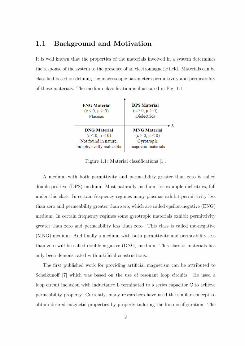
of these materials. The medium classification is illustrated in Fig. 1.1.
Figure 1.1: Material classifications [1].
A medium with both permittivity and permeability greater than zero is called
double-positive (DPS) medium. Most naturally medium, for example dielectrics, fall
under this class. In certain frequency regimes many plasmas exhibit permittivity less
than zero and permeability greater than zero, which are called epsilon-negative (ENG)
medium. In certain frequency regimes some gyrotropic materials exhibit permittivity
greater than zero and permeability less than zero. This class is called mu-negative
(MNG) medium. And finally a medium with both permittivity and permeability less
than zero will be called double-negative (DNG) medium. This class of materials has
only been demonstrated with artificial constructions.
The first published work for providing artificial magnetism can be attributed to
Schelkunoff [7] which was based on the use of resonant loop circuits. He used a
loop circuit inclusion with inductance L terminated to a series capacitor C to achieve
permeability property. Currently, many researchers have used the similar concept to
obtain desired magnetic properties by properly tailoring the loop configuration. The
2

major drawback in using metallic loops is the loss attributed with the conduction loss
in microwave and optical frequencies. In addition, the fabrication of metallic loops at
optical region is very challenging. The promising way to solve these problems is to
use a composite medium constructed of dielectric particles. This structure also has
the potential to offer a wider bandwidth. The first part of this dissertation focuses on
demonstration and development of DNG material by using all dielectric particles.
Metamaterial potential applications are diverse and include remote aerospace ap-
plications, sensor detection and infrastructure monitoring, smart solar power manage-
ment, public safety, radomes, high-frequency battlefield communication and lenses for
high-gain antennas, improving ultrasonic sensors and even shielding structures from
earthquakes. The research in metamaterials is interdisciplinary and involves such fields
as electrical engineering, electromagnetics, solid state physics, microwave and antennae
engineering, optoelectronics, classic optics, material sciences, semiconductor engineer-
ing, nanoscience and others [8]. In the second part of this dissertation the different
applications of metamaterials have been investigated and novel designs for nearfield
imaging and optical nanoantenna have been proposed.
1.1.1 Review of Research Efforts on Nearfield Imaging
Evanescent waves carry subwavelength information of an object. Amplifying these
modes and contributing them into the image plane has been a challenging task in
recent years. There are two sorts of electromagnetic radiation: near field and far
field. The latter propagates as plane waves with a real wave vector, the former has an
imaginary wave vector resulting in an exponential decay and therefore is confined to
the vicinity of the source. Conventional lenses act only on the far field: focusing the
near field requires amplification. Unfortunately for imaging purposes the finer details
of an object are contained in the near field. Based on Veselago’s work [6], Pendry
in [2] showed how a lossless negative index (NI) slab can realize a superlens to focus
3
all the Fourier components of a source. Later on, a series of research started to study
the different aspects of this topic and found out other possible ways to amplify the
evanescent waves [9–18]. Losses are the ultimate limiting factors for resolution and
even a highly conducting metal such as silver has a restricted performance. Redesigning
the lens to minimize absorption will help to attain improved subwavelength resolution.
To use a large magnitude of the real part of ε and to use a layered stack of alternating
negative-positive dielectric layers have been suggested to reduce the effect of losses [19–
21]. This gives a greatly improved performance, but even in these systems losses
eventually limit the resolution. Absorption in the lens materials will always limit the
attainable subwavelength resolution in any implementation. One possibility that arises
in optics is to use optical amplification to overcome absorption and this represents an
interesting option to increase the subwavelength resolution of these superlenses.
1.1.2 Review of Research Efforts on Antennas
The history of antennas dates back to James Clerk Maxwell who unified the theories
of electricity and magnetism, and eloquently represented their relations through a set
of profound equations best known as Maxwell’s Equations [22, 23]. His work was first
published in 1873 [24]. The first wireless electromagnetic system was demonstrated
by Heinrish Rudolph Hertz in 1886 and it was not until 1901 that Guglielmo Marconi
was able to send signals over large distances. From Marconi’s inception through the
1940s, antenna technology was primarily centered on wire related radiating elements
and frequencies up to about UHF. Modern antenna technology was launched while
World War II and beginning primarily in the early 1960s, numerical methods were
introduced that allowed complex antenna system configuration to be analyzed and
designed very carefully.
Antenna engineering has enjoyed a very successful period during the 1940s-1960s.
Although a certain level of maturity has been attained, there are many challenging
4

opportunities and problems to be solved. Integration of new materials into antenna
technology offers many opportunities. Because of the many new applications, the lower
portion of the EM spectrum has been saturated and the designs have been pushed to
higher frequencies, including the millimeter wave frequency bands. Smaller physical
size, wider bandwidth and higher radiation efficiency are three desirable characteristics
of antennas integrated into communication systems. In recent years, considerable
efforts have been devoted towards antenna miniaturization. The challenge is to make
the physical size of the antenna as small as possible along with achieving a wideband
impedance characteristic (Q values close to the lower-bound).
While antenna is a key element in the microwave spectrum to enable wireless data
communication, the extension of this concept into the optics has many applications
and has been a growing research in recent years. Among the technological applica-
tions for optical antennas one can find high-resolution microscopy and spectroscopy,
optical sensors, lasing, solar cells and efficient solid-state light sources, and it has also
become important in biotechnology and medicine. The metals used in antenna de-
signs in microwave/RF frequency domain are highly conductive materials, which in
the theory and the numerical simulation are often modeled as perfect electric conduc-
tors or, sometimes, a high-conductivity surface with certain surface impedance. In
optical domain, the metals behave very differently which means all the concepts and
experiments which have been done in microwave/RF domain cannot be used directly
in optical antenna design and must be re-examined. This opens up a new research
area which is growing so fast these days.
1.2 Dissertation Overview
This dissertation has 5 main chapters along with the Introduction chapter and a con-
clusion statement. We begin from the concept of demonstrating all-dielectric metama-
terial in Chapter 2. Then in following Chapters, we further present several applications
5

of metamaterials in focusing and radiation characteristics. A short description of the
chapters is summarized as below:
Chapter 2: All-Dielectric Metamaterials
In this chapter, physical concept and performance analysis of RF/optical all-dielectric
metamaterials are presented. It is demonstrated that a metamaterial with desired ma-
terial parameters (ε, µ) can be successfully developed by creating electric and magnetic
resonant modes. Dielectric disk and spherical particle resonators are considered as the
great candidates for establishment of dipole moments. A full wave Finite Difference
Time Domain (FDTD) technique is applied to comprehensively obtain the physical
insights of dielectric resonators. Near-field patterns are plotted to illustrate the de-
velopment of electric and magnetic dipole fields. Geometric-polarization control of
the dipole moments allows ε and µ to be tailored to the application of interest. All-
dielectric Double Negative (DNG) metamaterials are designed. Engineering concerns,
such as, loss reduction and bandwidth enhancement are investigated.
Chapter 3: Near-Field Focusing
This chapter reviews the concept of high-resolution imaging of a negative index mate-
rial (NIM) slab and compares its performance with the structure made based on the
idea of coupled surface-modes layers. Fourier-spectrum theoretical model and finite
difference time domain (FDTD) numerical approach are applied to comprehensively
characterize the structures and demonstrate the characteristics. It is highlighted that
if the loss is small, a NIM slab can provide a better performance at a farther distance
than the layered structure with the same thickness. However, considering a realistic
design with relatively large loss, the later will offer a more promising performance
to the loss and the image can be reconstructed in a farther distance from the object
cascading more number of thin-layers.
6
Chapter 4: Ellipsoidal Metamaterial Subwavelength Radiator
The resonance performance and Quality factor of electrically small ellipsoidal radi-
ators made of Epsilon Negative (ENG) material is investigated in this chapter. It
is demonstrated that the material polarization can successfully provide resonance ra-
diation at the negative material constitutive parameters. In principle, arbitrary low
resonant frequencies for a fixed antenna dimension can be achieved. The dependence
of resonant frequency on the shape of the structure is determined. Special attention is
devoted to the sphere, thin disk, and long rod, and physical insights into the radiation
characteristics and Q (or bandwidth) are highlighted.
Chapter 5: Optical Reflectarray Nanoantenna
In this chapter, we study the design of optical nanoantennas and antenna arrays based
on the surface plasmon resonance of plasmonic nanoparticles. We first review the
scattering resonance of plasmonic particles of uniform and concentric structures. Then
using the concept, the design of a reflectarray nanoantenna at optical frequencies whose
elements are nano-sized concentric spherical particles with the core made of ordinary
dielectrics and the shell made of a plasmonic material will be investigated. Modeling
approaches based on finite difference time domain (FDTD) numerical method and Mie
scattering theory are used to characterize and tune the reflectarray design.
Chapter 6: Optical Nanoloops Array Antenna
In this chapter, we create an optical nanoantenna array composed of parasitic plas-
monic loops where they can enhance radiation characteristics and direct the optical
energy successfully. Three metallic loops inspired by the concept of Yagi-Uda antenna
are optimized around the region where they feature high scattering performance to
control the radiation beam. The loop geometry in compared to the dipole configu-
7

ration has the benefit of using the available aperture in an effective way to provide
the higher directivity. The angular emission of the nanoloops array antenna is highly
directive for upward radiation.
Chapter 7: Conclusions and Future works
This chapter concludes this dissertation, summarizes its contributions, and presents
recommendations on future work.
8

Chapter 2
All-Dielectric Metamaterials:
Design and Development
2.1 Introduction
Metamaterials are receiving increasing attention in the scientific community in recent
years due to their exciting physical properties and novel potential applications [1–5].
To achieve a metamaterial with a desired figure of merit, it is required to first cre-
ate appropriate electric and magnetic dipole moments (in small-size scales) utilizing
available materials and then tailor their arrangement to the application of interest.
Basically, the electric and magnetic dipole moments can be envisioned as the alpha-
bet for making metamaterials. For instance, to achieve an artificial magnetism, the
most conventional approach is to implement metallic loops offering magnetic dipole
moments [25]. Conductor rods can be used for producing electric dipole moments [26].
Arrangements of these dipole moments can establish required material parameters, for
instance, a double negative (DNG) metamaterial behavior as depicted in Fig. 2.1.
Most of the metamaterial designs are constructed with the use of metallic elements.
The major drawbacks in using metallic inclusions are their conduction loss and fab-
rication difficulties, especially in the optical frequencies. In addition, they show very
9
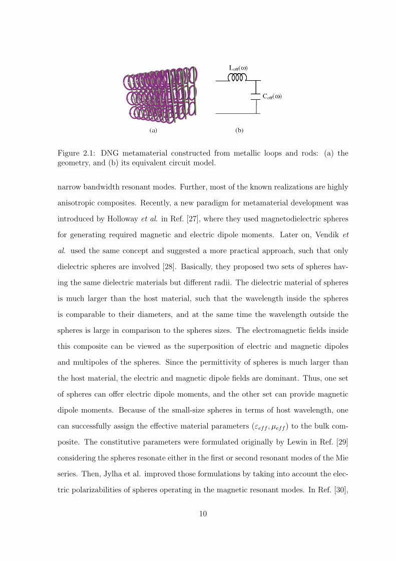
Figure 2.1: DNG metamaterial constructed from metallic loops and rods: (a) thegeometry, and (b) its equivalent circuit model.
narrow bandwidth resonant modes. Further, most of the known realizations are highly
anisotropic composites. Recently, a new paradigm for metamaterial development was
introduced by Holloway et al. in Ref. [27], where they used magnetodielectric spheres
for generating required magnetic and electric dipole moments. Later on, Vendik et
al. used the same concept and suggested a more practical approach, such that only
dielectric spheres are involved [28]. Basically, they proposed two sets of spheres hav-
ing the same dielectric materials but different radii. The dielectric material of spheres
is much larger than the host material, such that the wavelength inside the spheres
is comparable to their diameters, and at the same time the wavelength outside the
spheres is large in comparison to the spheres sizes. The electromagnetic fields inside
this composite can be viewed as the superposition of electric and magnetic dipoles
and multipoles of the spheres. Since the permittivity of spheres is much larger than
the host material, the electric and magnetic dipole fields are dominant. Thus, one set
of spheres can offer electric dipole moments, and the other set can provide magnetic
dipole moments. Because of the small-size spheres in terms of host wavelength, one
can successfully assign the effective material parameters (εeff , µeff ) to the bulk com-
posite. The constitutive parameters were formulated originally by Lewin in Ref. [29]
considering the spheres resonate either in the first or second resonant modes of the Mie
series. Then, Jylha et al. improved those formulations by taking into account the elec-
tric polarizabilities of spheres operating in the magnetic resonant modes. In Ref. [30],
10
HFSS software was also used to numerically model the periodic configuration where
the perfect electric conductor (PEC) and perfect magnetic conductor (PMC) surfaces
were located on the periodic sides of the structure. This method is applicable only if
the electric and magnetic fields are polarized normal to the PEC and PMC surfaces,
respectively. In a metamaterial, the electric and magnetic fields can, in general, be
polarized in complex forms inside the unit cell and applying this technique may not
be appropriate.
The advantages of only-dielectric metamaterial in comparison to its metallic coun-
terpart are the better potential for fabrication from RF to optics, and the higher
efficiency because of not having the metallic loss. In addition, one can achieve an
isotropic metamaterial design utilizing spherical geometry inclusions. Further, the di-
electric spheres offer wider bandwidth at the electric and magnetic eigenfrequencies
due to the larger fraction of unit-cell volume that they can occupy.
It is worth noting that if the goal is to achieve a DNG medium at optical frequencies,
one can use only one set of spheres (magnetic resonant mode), and embed them inside a
negative permittivity plasmonic host material, such as metals or semiconductors. This
idea was first proposed by Seo et al. in Ref. [31]. The obtained structure shows more
robust characteristics over the double-spheres lattice design in terms of fabrication
tolerance and bandwidth, although the loss of the host plasmonic medium (the metal)
can be an issue.
The goal of the present work is to provide a comprehensive investigation of dielectric
metamaterials. The physical insights and engineering concerns are addressed. We start
with the periodic photonic band-gap (PBG) crystals, and demonstrate how the band-
gap region is obtained as the result of periodicity along the propagation direction and
diffraction phenomena between the unit cells. The near-field patterns before and after
the gap region are plotted to better understand the PBG behavior. Then, we modify
the geometry of the PBG crystal by considering finite size disks instead of the infinite
rods. The performance is analyzed, and transmission coefficient and near-field patterns
11

are determined. It is illustrated that the dielectric disks can interestingly create electric
and magnetic dipole moments at their resonant modes, which can be successfully used
for the metamaterial development. This process is basically nothing to do with the
periodicity and unit-cell diffractions along the direction of propagation, and allows one
to accomplish a metamaterial with very small-size ingredients. The concept is extended
to spherical particles, and effective constitutive parameters (ε, µ) are presented. A
DNG all-dielectric metamaterial is designed. The dielectric metamaterial is free of
conduction loss and provides a relatively high efficiency. The periodic (or possible
random) arrangement of particles also suppresses the radiation loss that each of the
resonators produces individually. It is shown that by embedding the dielectric particles
close to each other, the couplings between them are increased, and the bandwidth
of a negative permittivity-negative permeability region is effectively enhanced. The
complex metamaterial structures designed in this study are modeled using an advanced
and versatile in-house developed finite difference time domain (FDTD) technique [32–
34].
2.2 Periodic Photonic Crystals
Photonic crystals are a novel class of periodic dielectric structures that by offering
engineered dispersion diagrams effectively manipulate the propagation of EM or op-
tical waves [35, 36]. The discovery of PBG crystals created unique opportunities for
proposing novel devices in both microwave and terahertz frequencies [37–39]. The
main benefit of PBG materials is their construction from all dielectric elements, which
increases their feasibility for fabrication from RF to optics. Although in the begin-
ning the focus was on the utilization of the stop-band region of PBG for controlling
the waves, recently, other applications such as directive emission, negative refraction,
superlensing, etc., with the use of other parts of the PBG dispersion diagram have
been highlighted [40, 41]. One fact that must be carefully considered is that the novel
12

behaviors of the PBG are derived from the unit-cell interactions and periodic dielec-
tric contrasts along the propagation direction, and one needs a specific unit-cell size
to achieve the required diffractions for accomplishing the performance of interest. The
problem is now twofold: first, the unit cell cannot be as small as one is interested in,
and second, the diffraction phenomenon degrades the performance of the PBG in some
specific applications such as directive emission or superlensing devices.
The simplest possible photonic crystal consists of alternating layers of material
with different dielectric constants. Fig. 2.2 depicts the geometry of a one-dimensional
periodic structure of dielectric layers (5-layers along the x) and its transmission coef-
ficient. The periodicity of structure along the x-direction opens up a stop-band region
between the dielectric and air modes.
(a) (b)
Figure 2.2: Periodic structure of dielectric slabs: (a) the geometry, and (b) its trans-mission coefficient.
A two-dimensional photonic crystal is periodic along two of its axes and homoge-
neous along the third. A typical specimen, consisting of a square lattice of dielectric
columns is shown in Fig. 2.3(a). For certain values of the column spacing, this crystal
can have a photonic band gap in the xy-plane. Inside the gap, no extended states
are permitted, and incident light is reflected. But although the multilayer film only
13
reflects light at normal incidence, this two-dimensional photonic crystal can reflect
light incident from any direction in the plane [36].
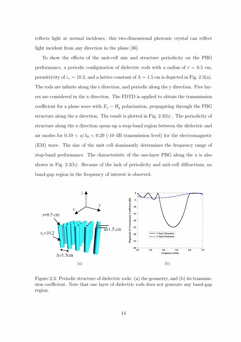
To show the effects of the unit-cell size and structure periodicity on the PBG
performance, a periodic configuration of dielectric rods with a radius of r = 0.5 cm,
permittivity of εr = 10.2, and a lattice constant of Λ = 1.5 cm is depicted in Fig. 2.3(a).
The rods are infinite along the z direction, and periodic along the y direction. Five lay-
ers are considered in the x direction. The FDTD is applied to obtain the transmission
coefficient for a plane wave with Ez −Hy polarization, propagating through the PBG
structure along the x direction. The result is plotted in Fig. 2.3(b) . The periodicity of
structure along the x direction opens up a stop-band region between the dielectric and
air modes for 0.19 < a/λ0 < 0.29 (-10 dB transmission level) for the electromagnetic
(EM) wave. The size of the unit cell dominantly determines the frequency range of
stop-band performance. The characteristic of the one-layer PBG along the x is also
shown in Fig. 2.3(b). Because of the lack of periodicity and unit-cell diffractions, no
band-gap region in the frequency of interest is observed.
(a)
2.0 3.0 4.0 5.0 6.0 7.0Frequency (GHz)
−40
−35
−30
−25
−20
−15
−10
−5
0
Mag
nitu
de o
f Tra
nsm
issi
on C
oeffi
cien
t (dB
)
5−layer Structure1−layer Structure
(b)
Figure 2.3: Periodic structure of dielectric rods: (a) the geometry, and (b) its transmis-sion coefficient. Note that one layer of dielectric rods does not generate any band-gapregion.
14

Figure 2.4: Near-field patterns for Ez in the x-y plane (one unit cell) for five-layerrods: (a) before band gap (f1 = 2.80GHz), and (b) after band gap (f2 = 6.60GHz).Note the confinement of dielectric and air modes inside the dielectric and air regions,respectively.
The Ez near-field patterns of five-layer PBG before and after the band-gap region
(at f1 = 2.80GHz and f2 = 6.60GHz) are shown in Fig. 2.4. It is observed that at
frequencies before the band gap the electric field is concentrated inside the dielectric
region, giving it a lower frequency, while the mode just above the gap has most of its
power in the air region, so its frequency is raised a bit. This satisfies the electromag-
netic variational theory applied to understand the PBG concept [36]. For the one-layer
PBG nearfield behaviors at f1 and f2 are obtained in Fig. 2.5, and one cannot observe
the similar phenomena as what was obtained for the five-layer case.
Therefore, to achieve a desired performance utilizing the PBG concept (periodic
dielectric contrast), having periodicity and a relatively large size unit cell are essential.
One might be able to reduce the size of the unit cell by increasing the permittivity of
the dielectric rod; however, this will increase the interactions between the unit cells
causing more diffractions along the propagation direction, which might not be suitable
for some applications. In the following sections, we will address how an engineered
dispersion diagram may be successfully tailored using a different concept that is based
15

Figure 2.5: Near-field patterns for Ez in the x-y plane (one unit cell) for one-layer rodsat (a) f1 = 2.80GHz, and (b) f2 = 6.60GHz.
on the creation of dipole modes inside the dielectric resonators. This will introduce a
unique paradigm for the development of functional metamaterials.
2.3 Dielectric Disks: Electric and Magnetic Dipole
Creation
In this section, we introduce the concept of electric and magnetic dipole moments,
and address their potential applications for metamaterial realization. To begin, let us
consider the five-layer PBG structure depicted in the previous section and modify the
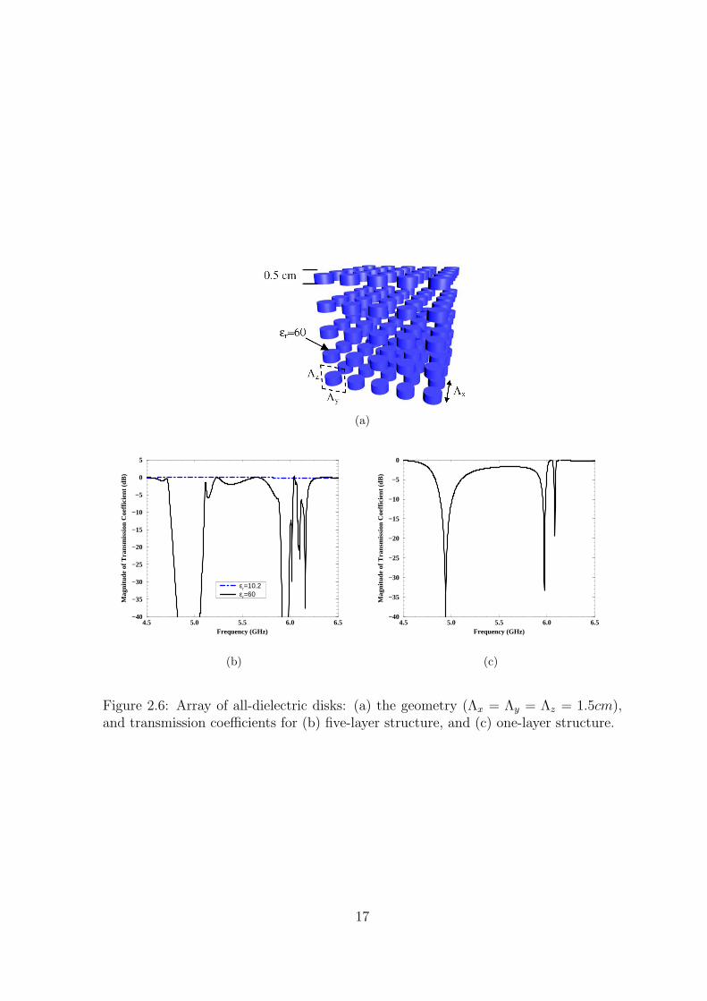
geometry by considering finite size disks with thickness L=0.5 cm. The geometry is
shown in Fig. 2.6(a). The FDTD is applied to characterize the structure and obtain
the transmission coefficient. The result is plotted in Fig. 2.6(b). No band-gap region
is observed. Now, we increase the permittivity of dielectric disks to εr = 60 such
that a stopband performance in the frequency range of 4.75 < f(GHz) < 5.10 can be
determined. Interesting enough, that even one layer of this design can also provide
the band-gap phenomenon around the same center frequency (f = 4.94GHz), having
of course a narrower bandwidth, as shown in Fig. 2.6(c).
16
(a)
4.5 5.0 5.5 6.0 6.5Frequency (GHz)
−40
−35
−30
−25
−20
−15
−10
−5
0
5
Mag
nitu
de o
f Tra
nsm
issi
on C
oeffi
cien
t (dB
)
εr=10.2εr=60
(b)
4.5 5.0 5.5 6.0 6.5Frequency (GHz)
−40
−35
−30
−25
−20
−15
−10
−5
0
Mag
nitu
de o
f Tra
nsm
issi
on C
oeffi
cien
t (dB
)
(c)
Figure 2.6: Array of all-dielectric disks: (a) the geometry (Λx = Λy = Λz = 1.5cm),and transmission coefficients for (b) five-layer structure, and (c) one-layer structure.
17

To provide a physical understanding of this phenomenon, the electric and magnetic
field patterns inside one unit cell of the one-layer disks array at f1 = 4.94GHz are
plotted in Fig. 2.7 (snapshot in time). One can observe that the near-field patterns
of the dielectric disk are very similar to those of a magnetic dipole oriented along
the y direction. The near-field patterns at the second and third resonant frequencies
f2 = 5.97GHz and f3 = 6.08GHz are also plotted in Figs. 2.8 and 2.9, respectively.
The disk at the second resonant frequency is almost equivalent to an electric dipole
located along the z axis. The third mode has a resonant frequency very close to the
second mode, and its magnetic field pattern in the equatorial plane exhibits an octupole
characteristic, consisting of two linear quadrupoles rotated by 90 with respect to each
other. Higher order resonant modes can also be generated by the dielectric disks
utilizing the mutipole modes.
Because of the very large permittivity material of the dielectric disk, one can con-
sider the structure as a resonator where most of the fields are localized inside the
medium. Kejfez et al. have performed a comprehensive study of dielectric resonators
in Ref. [42], and clearly illustrated the potential of dielectric cylindrical resonators for
providing electric and magnetic dipole moments. Semouchkina et al. have also noticed
the differences between the field patterns of infinite rods PBG and finite-size cylin-
ders [43]. Peng et al. have also recently illustrated the electric and magnetic mode
development inside the very high permittivity rods [44]. Considering the polarization
of the plane wave excitation, the three resonant frequencies obtained in Fig. 2.6(c)
can be attributed to HEM11, TM01, and HEM21 resonant modes, respectively [42].
The near-field patterns for an isolated finite-size cylinder for the above resonant modes
have been plotted in Ref. [42], and they closely resemble what has been demonstrated
here for the periodic array of the disks. Hence, the stop-band regions in Fig. 2.6(c)
are derived from the resonant modes of the isolated disks, and thus even one layer of
the structure can provide the band-gap property of interest.
The HEM11 mode is sometimes called unconfined mode, because in the limit, as
18

Figure 2.7: Field distributions inside one unit cell of the one-layer disks array atf1 = 4.94GHz (HEM11δ mode): (a) E in the x-z plane, and (b) H in the y-x plane.Near fields are similar to those of a magnetic dipole oriented along the y direction.
Figure 2.8: Field distributions inside one unit cell of the one-layer disks array atf1 = 5.97GHz (TM01δ mode): (a) E in the y-z plane, and (b) H in the y-x plane. Nearfields are similar to those of an electric dipole oriented along the z direction.
19

Figure 2.9: Field distributions inside one unit cell of the one-layer disks array atf3 = 6.08GHz (HEM21δoctupole mode): (a) E, and (b) H in the y-x plane.
εr → ∞, its magnetic field does not vanish on the surfaces of the cavity resonator.
This can be revealed from Fig. 2.7, where the magnetic field is normal to the magnetic
wall boundary of the cavity and cannot be zero in the limiting case. In contrast, the
TM01 mode is of the confined type, since its magnetic field is tangent to the boundary
of the cavity, and in the limit, as εr → ∞, it must be zero along the surface (see
Fig. 2.8). The mode confinement behavior can also be readily seen by looking at the
transmission coefficient plot in Fig. 2.6(c) , where the HEM11 mode (magnetic dipole)
presents a lower Q than the TM01 mode (electric dipole). The octupole performance
of the HEM21 mode represents an inefficient radiator and consequently, its Q factor
is very large. It is worth noting that although each of the disk resonators individually
has some radiation loss, when we arrange them in the periodic fashion, the couplings
between them are increased and the radiation loss is considerably suppressed.
Tailoring the dielectric disks allows one to successfully control the physical perfor-
mance of the design. For example, as mentioned earlier, the resonant frequency of the
HEM21 mode is very close to the electric dipole mode TM01, and if the TM01 mode
is the desired mode of operation, the HEM21 mode may create an undesirable nearby
resonance effect, and one might be interested in suppressing it. This can be simply
20

accomplished by placing a thin wire loop on the end face of the disk resonator where
the electric field has a strong component, or, for instance, since the TM01 mode has a
relatively strong electric field along the axis of rotation, it is possible to tune this mode
by removing the cylindrical center section (leaving a doughnut shape) and replacing
it by a movable dielectric rod.
In summary, the important conclusion of this section is the fact that dielectric
resonators can successfully provide electric and magnetic dipole modes. The dipole
moments can be considered as the alphabet for making metamaterials. For instance,
using an array structure of the magnetic dipole disks (one layer) one can effectively
provide a band-gap medium. The major advantage compared to the PBG concept
is that the unit-cell interaction along the propagation directions is not required for
achieving the functionality of interest. Basically, each of the disks itself provides the
required resonant behavior. In general, by tailoring the electric and magnetic dipole
moments in one unit cell one can make a building-block cell with the figure of merit
of interest. Then, by making a material from these small-size cells, one can claim a
metamaterial design with the homogeneous effective constitutive parameters εeff , µeff .
This will be described in more detail in the next section.
2.4 Metamaterial Realization
The materials presented in the previous section are very helpful in providing a phys-
ical understanding of the dipole modes generation utilizing dielectric resonators. In
this section, we apply this concept to design spherical particle-based metamaterials.
Fig. 2.10(a) shows a periodic array of dielectric spheres having high permittivity εp
embedded inside the nonmagnetic host matrix εh. The structure has an isotropic unit
cell. Using Mie theory, one can express the EM waves of each sphere as an infinite series
of spherical vector functions Mn and Nn. Applying the field transformation between
the nonconcentric spheres, and using the boundary conditions, the array of spheres
21

can be solved analytically [29, 45]. It is assumed that the size of the spheres is compa-
rable to their material wavelength, and small in terms of host material wavelength, so
that the effective material parameters can be accurately defined for the structure. As
demonstrated earlier, the dielectric resonators can offer electric and magnetic dipole
moments, and higher order modes. Indeed, from the Mie series, it clears that the dom-
inant modes (n=1) are TE (magnetic dipole) and TM (electric dipole) waves. Around
the eigenfrequencies of these modes one can assume the existence of only the electric
and magnetic modes and obtain the effective material parameters εeff , µeff for the
periodic spheres as [27]
εeff = εh
(1 +
3νf
εpF (θ)+2εh
εpF (θ)−εh− νf
), (2.1a)
µeff = µ0
(1 +
3νf
F (θ)+2F (θ)−1
− νf
), (2.1b)
where νf is volume fraction of the spheres, and function F (θ) is
F (θ) =2(sin θ − θ cos θ)
(θ2 − 1) sin θ + θ cos θ, (2.2)
with
θ = k0r√
εp,r, (2.3)
where r is the radius of spheres. It is interesting to emphasize that the nonmagnetic
spheres can create magnetism due to the magnetic dipole polarization.
The effective constitutive parameters of the periodic spheres depicted in Fig. 2.10(a),
having dielectric constant εp,r = 40, radius r = 0.5cm, and unit-cell size Λx = 1.5cm,
Λy = Λz = 2.5cm, are plotted in Fig. 2.10(b). The first resonant frequency at
fm = 4.72GHz is associated with the magnetic mode and the second resonance at
fe = 6.61GHz represents the electric mode. As described earlier, the magnetic mode
is an unconfined mode and provides a wider bandwidth. This can be seen from
22

Figure 2.10: Array of one-layer all-dielectric spheres: (a) the geometry (Λy = Λz =2.5cm), and (b) its effective constitutive parameters.
Fig. 2.10(b) and Eq. (2.1), where one can find a larger bandwidth for the TE res-
onance in comparison to the TM resonance by a factor of about εp/εh. It is worth
noting that above the resonant frequencies of magnetic and electric modes, negative
permeability and negative permittivity materials are established, respectively. This
will be used later in this section for the metamaterial realization of DNG behavior.
The FDTD is applied to characterize the structure and obtain the transmission
coefficient for a plane wave propagating through the medium (one layer along x). The
result is shown in Fig. 2.11. Comparing Fig. 2.10(b) with Fig. 2.11, one can observe
that the analytical formulations (2.1) closely estimate the first two resonant frequencies
determined through the FDTD full wave analysis (less than 1% error). However, as
expected, the third resonant frequency at f =6.73 GHz cannot be predicted based on
Eq. (2.1). In practice, the third resonant frequency can set an upper limit on the
frequency band of the second mode where the effective permittivity is defined. It is
interesting to note that the transmission coefficient behavior of the dielectric spheres is
very similar to that of the dielectric disks see Fig. 2.6(c). The near-field distributions
are plotted in Fig. 2.12 for the first two resonant frequencies (fm = 4.73GHz and
fe = 6.55GHz) and clearly validate the existence of magnetic and electric dipole
23

polarizations.
4.0 4.5 5.0 5.5 6.0 6.5 7.0 7.5Frequency (GHz)
−40
−35
−30
−25
−20
−15
−10
−5
0
Mag
nitu
de o
f Tra
nsm
issi
on C
oeffi
cien
t (dB
)
Figure 2.11: Transmission coefficient for the all-dielectric spheres depicted inFig. 2.10(a). The first and second resonances represent magnetic and electric reso-nant modes, respectively.
So far, we have described how one can successfully realize a metamaterial with both
electric and magnetic parameters utilizing only-dielectric resonators, fulfilling desired
effective constitutive parameters. The next step is to investigate the possibility of
increasing the bandwidth of the resonant modes. But, first let us clear one issue.
Consider, for instance, the magnetic resonant mode of the one-layer periodic spheres
[Fig. 2.10(a)], having -10 dB bandwidth of about BW = 1.2%. It is well understood
that each of the cavity resonators can be considered as a parallel LC circuit. Cascad-
ing the LC resonant circuits can increase the transmission coefficient bandwidth. In
fact, increasing the number of layers (parallel LC circuits) increases the transmission
coefficient bandwidth. However, it should be noticed that this is nothing to do with
the bandwidth of the metamaterial. The performance of three layers of the spheres
designed in Fig. 2.10(a) is shown in Fig. 2.13. The transmission bandwidth is increased
from 1.2% to about 4.6%; but, both one-layer and three-layer structures have almost
the same µeff given by Eq. (1b), and of course the similar permeability bandwidth.
Increasing the number of layers will simply increase the thickness of the structure.
In this work, a very unique approach for the bandwidth enhancement of metama-
24

Figure 2.12: Field distributions inside one unit cell of the spheres array: (a) E inthe x-z plane and H in the y-x plane at fm = 4.73GHz, representing the magneticdipole moment, and (b) E in the y-z plane and H in the y-x plane at fe = 6.55GHz,representing the electric dipole moment (1.5cm × 1.5cm of the unit cell in the y-zdirections is plotted).
(a)
4.0 4.5 5.0 5.5 6.0 6.5 7.0 7.5Frequency (GHz)
−40
−35
−30
−25
−20
−15
−10
−5
0
Mag
nitu
de o
f Tra
nsm
issi
on C
oeffi
cien
t (dB
)
(b)
Figure 2.13: Array of three-layer dielectric spheres (Λx = 1.5cm): (a) the geometry,and (b) its transmission coefficient.
25
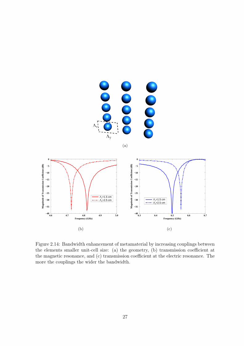
terials is presented. Recently, Mosallaei et al. demonstrated how the bandwidth of
the negative permeability medium realized utilizing metallic embedded-loop circuits
can be improved by increasing the couplings between the loop elements [34]. In fact,
based on their circuit model analogy it is shown that the bandwidth of the negative
permeability medium depends strongly on the coupling coefficient κ between the loops,
and can be estimated from the following equation:
∆ω
ωp
=1√
1− κ2− 1, (2.4)
where ωp is the resonant frequency of the loops, and κ < 1. The higher the coupling
coefficient κ the larger the bandwidth. This concept is applied here to the all-dielectric
metamaterial design. Basically, we increase the couplings between the spheres shown
in Fig. 2.10(a), by bringing them closer to each other along the z direction, namely,
assuming Λz = 1.5cm [Fig. 2.14(a)]. Transmission coefficient for the magnetic mode
is plotted in Fig. 2.14(b) illustrating a bandwidth enhancement of more than 100%
compared to the original design Λz = 2.5cm. An almost similar observation for the
electric mode resonance is illustrated in Fig. 2.14(c) (bandwidth is increased from 0.5%
to 1.3%). Basically, when we make the spheres closer to each other, the mode radiation
through the spheres is increased causing the reduction in the Q factor of each of the
spheres, resulting in the bandwidth enhancement of the resonant modes. Slight shifts
in the resonant frequencies due to the coupling effects are also noted.
We will now investigate the development of double negative metamaterials using
dielectric resonators. As highlighted earlier, and can be seen from Fig. 2.10(b), the
periodic array of dielectric spheres can generate both negative effective permeability
and permittivity, however, at different resonant frequencies (fm = 4.72GHz, fe =
6.61GHz). To obtain a DNG behavior around the same resonant frequency, a building-
block unit cell constructed from two spheres having the same size but different dielectric
constants εp1,r = 40 and εp2,r = 23.8, is optimized in Fig. 2.15(a). The set of spheres
26
(a)
4.6 4.7 4.8 4.9 5.0Frequency (GHz)
−40
−35
−30
−25
−20
−15
−10
−5
0
Mag
nitu
de o
f Tra
nsm
issi
on C
oeffi
cien
t (dB
)
Λz=1.5 cmΛz=2.5 cm
(b)
6.3 6.4 6.5 6.6 6.7Frequency (GHz)
−40
−35
−30
−25
−20
−15
−10
−5
0
Mag
nitu
de o
f Tra
nsm
issi
on C
oeffi
cien
t (dB
)
Λz=1.5 cmΛz=2.5 cm
(c)
Figure 2.14: Bandwidth enhancement of metamaterial by increasing couplings betweenthe elements smaller unit-cell size: (a) the geometry, (b) transmission coefficient atthe magnetic resonance, and (c) transmission coefficient at the electric resonance. Themore the couplings the wider the bandwidth.
27

(a)
6.1 6.2 6.3 6.4 6.5 6.6 6.7 6.8 6.9Frequency (GHz)
−40
−35
−30
−25
−20
−15
−10
−5
0
Mag
nitu
de o
f Tra
nsm
issi
on C
oeffi
cien
t (dB
)
εr=23.8εr=40Double−sphere Struc.Loss Tangent=.001
(b)
Figure 2.15: DNG metamaterial constructed from all-dielectric spheres: (a) the geom-etry (Λy = 2.5cm, Λz = 1.5cm), and its equivalent circuit model, and (b) transmissioncoefficient.
with εp1,r = 40 creates negative effective permittivity about fe = 6.50 GHz, and the
set of spheres with εp2,r = 23.8 generates negative effective permeability about fm =
6.29GHz. Fig. 2.15(b) presents transmission coefficients of both sets, where stop-band
regions are determined in the negative material frequency ranges. It must be mentioned
that in the constructed lattice of both spheres [Fig. 2.15(a)], the electric mode has a
higher Q compared to the magnetic mode, and hence, the coupling effect of the sphere
with dielectric εp2,r = 23.8 on the electric resonance should be larger than that of
the sphere with dielectric εp1,r = 40 on the magnetic resonance. This phenomenon
is carefully explained from another point of view in Ref. [30]; as it is discussed the
electric polarizability of the dielectric sphere operating in the magnetic resonance has
an influence on the electric mode sphere, causing the electric resonance of the double-
sphere lattice to be slightly lower than that of the single-sphere lattice (less than 1
shift). The magnetic resonance stays almost the same (nonmagnetic spheres). Thus,
in Fig. 2.15(b), the electric resonance of the single-sphere lattice should be slightly
shifted down to envision the negative permittivity region of the doublesphere lattice.
28

Considering this, a region with both negative ε and µ is accomplished. Transmission
coefficient for the double-sphere unit cell is shown in Fig. 2.15(b), demonstrating an
almost total transmission in the DNG region, around f=6.42 GHz. The phase of
the field distribution at f=6.42 GHz inside one layer of the metamaterial is shown in
Fig. 2.16. The positive slope for the phase in the central region of the layer clears the
establishment of the DNG medium (backward wave). The electric and magnetic field
intensities inside the unit cell at this frequency are also shown in Fig. 2.17. One can
clearly observe the development of electric and magnetic dipole modes that provide
the required effective material parameters. This also validates the existence of the
dipolar modes assumption, made in the derivation of Eq. (2.1). The effect of the loss
is also studied, by considering spheres with a dielectric loss tangent of tanδ = 0.001.
The result is plotted in Fig. 2.15(b), illustrating less than -1 dB transmission loss in
the DNG region. Utilizing dielectric materials with better loss tangents can of course
provide a higher efficiency.
The same concept can be used to design a DNG metamaterial realized utilizing
dielectric disks, which might be easier for fabrication in some cases. The geometry is
depicted in Fig. 2.18(a). Transmission coefficients and field patterns at f =5.97 GHz
are evaluated in Figs. 2.18(b) and 2.19. Similar observations as the spherical particles
are accomplished.
2.5 Optical Metamaterials
Realization of metamaterials at terahertz frequencies is also of great interest due to the
possibility of designing novel nanoscale devices in the infrared and visible regimes [46–
51]. The concept of all-dielectric metamaterials can be extended to the optical fre-
quencies; however, because of the fabrication limitations one needs to use smaller value
dielectric materials for the resonating inclusions. In this case, larger-size resonators
may be implemented. Fig. 2.20(a) depicts an array of gallium phosphide (GaP) spheres
29

Figure 2.16: Phase distribution of the electric field Ez inside the layer of DNG meta-material [Fig. 2.15(a)] at f = 6.42GHz. The plane wave propagates from left to theright where the phase is increased in this direction. The positive slope for the phasein the central part of the layer is a demonstration of the backward wave generation.
with permittivity 12.25 and a dielectric loss tangent of tanδ = 0.001. The diameter
of spheres is 170 nm. Transmission coefficient performance is shown in Fig. 2.20(b),
where the development of magnetic and electric resonant modes can be observed. One
must notice that because of the low dielectric material of the spheres and their rela-
tively large physical size the couplings between the resonators are increased. This will
generate some difficulty in tuning the DNG medium if two sets of spheres are used.
Although the existing coupling may not be desirable from the fact that the electric
and magnetic resonances are coupled, it can be beneficial from the point that one can
successfully tailor a backward wave using the strong interaction between the spheres.
Work is currently under progress in this direction.
Alternative approaches will be to embed one set of dielectric spheres inside a plas-
monic host medium as obtained by Seo et al. [31]; or to use Drude material coated
spheres as proposed by Wheeler [51]. Here, we investigate the former method by
characterizing the performance of the periodic array of GaP spheres implanted inside
cesium (Cs) host material with a measured plasma wavelength λp = 0.41µm and a
damping constant γ of 51× 1012 [31], shown in Fig. 2.21(a). Note that if one operates
close to the plasma frequency, the index of host material is small, and physically large-
30

(a) (b)
(c)
Figure 2.17: Field distributions inside one unit cell of the DNG metamaterial[Fig. 2.15(a)] at f = 6.42GHz: (a) E in the y-z plane, (b) H in the y-x plane, and (c)E in the x-z plane. Note the creation of electric and magnetic dipole moments insidethe unit cell of the spheres of εr = 40 and εr = 23.8.
31

(a)
5.8 5.9 6.0 6.1 6.2Frequency (GHz)
−40
−35
−30
−25
−20
−15
−10
−5
0
Mag
nitu
de o
f Tra
nsm
issi
on C
oeffi
cien
t (dB
)
εr=43εr=60Double−disc Struc.Loss Tangent=.001
(b)
Figure 2.18: DNG metamaterial constructed from all-dielectric disks: (a) the geometry(Λy = 2.5cm, Λz = 1.5cm), and (b) its transmission coefficient.
Figure 2.19: Field distributions inside one unit cell of the DNG metamaterial[Fig. 2.21(a)] at f = 5.97GHz: (a) E in the y-z plane, and (b) H in the y-x plane.Note the creation of electric and magnetic dipole moments inside the unit cell of thedisks of εr = 60 and εr = 43.
32
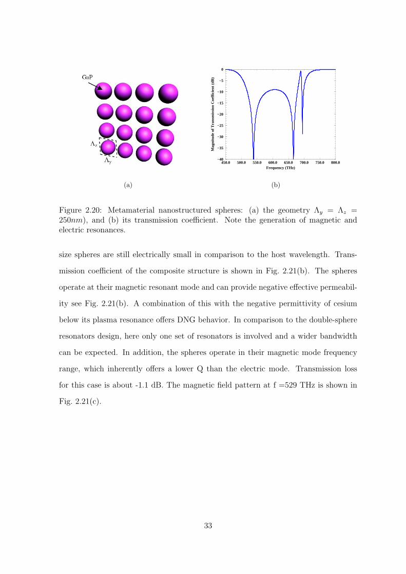
(a)
450.0 500.0 550.0 600.0 650.0 700.0 750.0 800.0Frequency (THz)
−40
−35
−30
−25
−20
−15
−10
−5
0
Mag
nitu
de o
f Tra
nsm
issi
on C
oeffi
cien
t (dB
)
(b)
Figure 2.20: Metamaterial nanostructured spheres: (a) the geometry Λy = Λz =250nm), and (b) its transmission coefficient. Note the generation of magnetic andelectric resonances.
size spheres are still electrically small in comparison to the host wavelength. Trans-
mission coefficient of the composite structure is shown in Fig. 2.21(b). The spheres
operate at their magnetic resonant mode and can provide negative effective permeabil-
ity see Fig. 2.21(b). A combination of this with the negative permittivity of cesium
below its plasma resonance offers DNG behavior. In comparison to the double-sphere
resonators design, here only one set of resonators is involved and a wider bandwidth
can be expected. In addition, the spheres operate in their magnetic mode frequency
range, which inherently offers a lower Q than the electric mode. Transmission loss
for this case is about -1.1 dB. The magnetic field pattern at f =529 THz is shown in
Fig. 2.21(c).
33

(a)
475.0 500.0 525.0 550.0 575.0 600.0Frequency (THz)
−40
−35
−30
−25
−20
−15
−10
−5
0
Mag
nitu
de o
f Tra
nsm
issi
on C
oeffi
cien
t (dB
)
Single−sphere Struct.Plasmonic HostDNG Material
(b) (c)
Figure 2.21: DNG optical metamaterial constructed from nanostructured dielectricspheres (operating in magnetic mode) embedded in negative permittivity host: (a) thegeometry, (b) transmission coefficient, and (c) H field in the y-z plane at f = 529THz.
34

2.6 Dispersion Diagram Characteristics of Periodic
Array of Dielectric Spheres
Dispersion diagrams are a useful approach to describe the modal behavior of electro-
magnetic structures. The bandgaps are typically visualized and investigated by com-
puting the dispersion relationship, ω(k), between the temporal and spatial frequencies
of the modes that can propagate in the particular periodic structure of interest. In this
thesis we applied the FDTD numerical method to calculate the dispersion diagrams.
One can find the details about dispersion diagrams and our approach to obtain them
in Appendix A.
In this section, we apply the dispersion diagram modeling tool to characterize the
performance of array of dielectric spheres and explore the development of dielectric
metamaterials. As mentioned earlier, to obtain the backward wave and DNG behav-
iors, appropriate electric and magnetic dipole moments should be created in building-
block unitcells of array configurations. In order to design such a structure, we use a
3D array of two different spheres as a unit-cell; where the spheres have the same sizes
and different materials. The challenge is to establish both the electric and magnetic
dipole resonances around the same frequency band.
Fig. 2.22 shows the geometry and the parameters of the array of spheres. The
performance of the first set described with εr = 40 is plotted in Fig. 2.22(b). In
the dispersion diagram two stop bands (gaps) are observed. The first stop band is
associated with the magnetic resonance where the second band is associated with the
electric resonance. Notice that, the first gap has a wider bandwidth in compared to
the second one. For the other set of sphere with the same geometry but εr = 21, only
the first band gap (magnetic resonance) is shown in the frequency spectrum of interest
in Fig. 2.22(c). As seen by comparing these two diagrams, the electric gap of the first
set and the magnetic gap of the other set are around the same frequency region.
35

Fig. 2.23 shows the dispersion diagram for the two-sets of 3D dielectric spheres.
By combining the two-sets, or basically by uniting the electric and magnetic dipole
modes, a negative slope backward wave behavior is achieved.
(a)
0 0.5 1 1.5 2 2.5 30
0.5
1
1.5
2
2.5
β Λx
k Λ
x
(b)
0 0.5 1 1.5 2 2.5 30
0.5
1
1.5
2
2.5
β Λx
k Λ
x
(c)
Figure 2.22: (a) The geometry of a 3D array of spheres: Λy/a = Λz/a = 5 andΛx/a = 3. Dispersion diagram for one-set of dielectric spheres with permittivity: (b)ε = 40 and, (c) ε = 21.
2.7 Conclusions
In this study, a comprehensive investigation of all-dielectric metamaterials is addressed.
The FDTD full wave analysis is applied to characterize the interactions of EM-optical
waves with the periodic array of metamaterials, and tailor required designs. Electric
36

0 0.5 1 1.5 2 2.5 30
0.5
1
1.5
2
2.5
β Λx
k Λ
x
Figure 2.23: Dispersion diagram for a DNG metamaterial constructed from two-setsof dielectric spheres with permittivities 40 and 21. Λy/a = Λz/a = 5 and Λx/a = 3.
and magnetic near-field patterns are established to highlight the physical insights.
Photonic crystals are searched first, and it is described that the band-gap phe-
nomenon appears as a result of the periodic dielectric contrasts along the propagation
direction. Then, the concept of electric and magnetic dipole modes generation for
metamaterial development is presented. Dielectric disk and spherical particle res-
onators are implemented to create required dipole moments. Arrangements of electric
and magnetic dipole moments in one unit cell tailor the metamaterial to the applica-
tion of interest. The beauty of the developed metamaterial is that even one unit cell of
the structure can provide the figure of merit of interest, and the interactions between
the cells is not essential, as was the case for the PBG. This will allow for making the
small-size unit cell, and defining the effective constitutive parameters accurately. Fur-
ther, a random arrangement might have the potential of offering the similar desired
properties, especially in the spherical resonator case where the unit cell is isotropic.
The physics of electric and magnetic dipole moments are explored. It is shown that
the magnetic resonance is an unconfined mode and has a lower Q than the confined
electric resonant mode. A unique approach is proposed to increase the bandwidth of
the resonant particles. Basically, by bringing the dielectric resonators closer to each
other, the radiation couplings between them are increased, resulting in lowering the
37

Q of each of the resonators. This will establish bandwidth enhancement. Dielectric
metamaterials are free of conduction loss and can provide high efficiency performance.
A DNG metamaterial constructed from two sets of spheres, having the same size
but different materials, is developed. One set of spheres provides negative permittiv-
ity, and the other set offers negative permeability, accomplishing the double negative
metamaterial. One can also design a double-sphere lattice DNG metamaterial using
the spheres of different sizes but having the same materials. Development of negative
index media at terahertz frequencies using plasmonic materials is also studied.
In general, all-dielectric metamaterials appear very promising for addressing some
of the important physical and engineering concerns, such as the loss and bandwidth.
They are quite feasible for fabrication in both microwave and IR-visible spectrums.
38

Chapter 3
Near-Field Focusing
3.1 Introduction
Evanescent waves carry subwavelength information of an object. Amplifying these
modes and contributing them into the image plane has been a challenging task in recent
years. Based on Veselago’s work [6], Pendry in [2] showed how a lossless negative index
(NI) slab can realize a superlens to focus all the Fourier components of a source. Later
on, a series of research started to study the different aspects of this topic and found
out other possible ways to amplify the evanescent waves [9–18]. Basically amplifying
the evanescent waves and tailoring the phase of propagating waves are two important
features which occur in imaging. To figure out the effect of each factor, one can study
the Fourier spectrum analysis to follow the behavior of waves in propagating and
evanescent regions. Other important issues in a realistic negative index material (NIM)
are the effects of material frequency dispersion and the loss that can considerably
degrade the performance. Then, the main engineering concern will be how far from
an object one can reconstruct the image with a high-resolution feature.
The goal of the present work is to provide an engineering investigation of imaging
performance of a NIM slab and compare its performance with coupled layered struc-
tures functioning based on the surface waves amplification. As known, a slab of NIM
39
can only manipulate the image in the transverse plane and a depth reconstruction
cannot be achieved. Further, for transverse pattern resolution, one needs to be close
to the surface to achieve better resolution of the object. Making a bulk material of
NIM with negative permittivity and negative permeability effective materials is also a
real challenge. Besides these, due to relatively large thickness of the slab, material loss
will considerably degrade the image performance of the structure. Therefore, in spite
of many interesting phenomena of NIM, not many practical applications for them have
been realized.
Basically, as amplification of evanescent waves and carrying them to the image
plane is a key to high-resolution imaging, coupled plasmon surface modes concept can
be a great alternative for realizing high-resolution near-field imaging. Decaying fields
can efficiently launch the surface waves along epsilon negative (ENG) or mu negative
(MNG) surfaces. Basically, Pendry in [2] showed how a thin ENG slab can be used for
near field imaging and later Ramakrishna et al discussed in [19–21] how the idea can
be extended to layered structures where the coupling between the surface-modes layers
determines a farther distance recognition. This canalization through the layers was
also studied by P.A. Belov et al in [52] and X. Li et al in [53]. ENG plasmonic surfaces
will respond only to p-polarized waves. To achieve a high-resolution imaging device
functioning properly for both p and s waves, one needs to integrate the ENG layers
with MNG interfaces. The resonance and tunneling performance of pairing an ENG
slab with a MNG slab has been studied by Alu et al in [47, 54] where they define a
conjugate-matched pair to guarantee zero-reflection and total-transmission conditions
for any plane wave impinging on the pair.
The objectives of this chapter are to investigate near field imaging performance of
coupled multi-layered structures of ENG and MNG surfaces, and to provide a com-
parative study with the NIM slab imaging behavior. Theoretical formulations and
dispersion diagram analysis are performed to comprehensively investigate the concept
and demonstrate unique characteristics. An advanced Finite Difference Time Domain
40

(FDTD) technique [32, 34] is also applied to characterize the finite-size composite
ENG-MNG layered validating our theoretical illustrations. The fields inside the layers
and in the transverse planes are obtained carefully. It is demonstrated that for the
layered structure since the thicknesses of the layers are relatively thin, the structure
is not very sensitive to the material loss as is experienced for the NIM configuration.
The construction of an ENG-MNG layered structure can be simpler than a NIM bulky
material, as one can use novel metallic patterns to realize it.
3.2 Theory and Formulation of Layered Structures
To characterize theoretically the performance of a layered structure, a Fourier spectrum
analysis is applied. Let us consider an arbitrary electric dipole oriented along the u
direction (with angle α with respect to z-axis), located at distance d1 in front of an
N-layer structure stacked along the z direction, as depicted in Fig. 3.1. Using the
dyadic Green’s function approach the field due to a Hertzian dipole is given by
E(r) =iωµ(I +∇∇k2
).αIleikr
4πr(3.1a)
H(r) =∇× αIleikr
4πr(3.1b)
where Il is the current moment and k = ω√
µε. When a point source is located next
to a layered medium, it is then best to decompose the field in terms of waves of TM
type and TE type. By expanding the field into plane waves with the Sommerfeld
identity [55, 56],
eik0r
r=
i
2
∫ ∞
−∞dkρ
kρ
kz
H(1)0 (kρρ) eikz |z| (3.2)
the field for the vertical electric dipole (the normal component of the excitation) is
characterized by [56]
41

Figure 3.1: The configuration of layered medium
Eiz =−Il
8πωεi
cos α
∫ ∞
−∞dkρ
k3ρ
k1z
H(1)0 (kρρ) Ai
[eikiz |z| + RTM
i,i+1eikiz(z+2di)
](3.3a)
Hiz =0 (3.3b)
and for the tangential component the field is
Eiz =iIl
8πωεi
sin α cos φ
∫ ∞
−∞dkρk
2ρH
(1)1 (kρρ) Ai
[±eikiz |z| − RTM
i,i+1eikiz(z+2di)
](3.4a)
Hiz =iIl
8πsin α sin φ
∫ ∞
−∞dkρ
k2ρ
k1z
H(1)1 (kρρ) Ai
[eikiz |z| + RTE
i,i+1eikiz(z+2di)
](3.4b)
where kz =√
k20 − k2
ρ for propagating components and kz = i√
k2ρ − k2
0 for evanes-
cent waves which decay exponentially with the z direction. RTMi,i+1 and RTE
i,i+1 are the
reflection coefficients for TM and TE modes, respectively and i stands for the layer
number. In general, for an N-layer medium, the generalized reflection coefficient at
the interface between region i and i + 1 called Ri,i+1, can be obtained as [56],
Ri,i+1 =Ri,i+1 + Ri+1,i+2e
2iki+1,z(di+1−di)
1 + Ri,i+1Ri+1,i+2e2iki+1,z(di+1−di). (3.5)
42

where Ri,i+1 is the Fresnel reflection coefficient for TE and TM modes as,
RTEi,i+1 =
µi+1kiz − µik(i+1)z
µi+1kiz + µik(i+1)z
(3.6a)
RTMi,i+1 =
εi+1kiz − εik(i+1)z
εi+1kiz + εik(i+1)z
(3.6b)
The coefficients Ais are also obtained by applying the boundary conditions through
a recursive process. Then the field can be represented in terms of Fourier spectrum such
that at any plane it is the summation of the propagating and evanescent components
as
Ez =
∫
k2ρ≤k2
0
EPropag.z (kρ, kz)dkρ +
∫
k2ρ>k2
0
EEvan.z (kρ, kz)dkρ (3.7)
Equations (3.3) and (3.4) will provide detailed information about the surface wave
propagation in coupled positive-negative layered structures and their poles manipula-
tion. It will be used in the following sections to successfully tailor imaging character-
istics.
3.3 Negative Index Material Slab
In this section we will review the performance of a NIM slab in propagation and
transverse planes. This will be accomplished with the use of equations derived in the
previous section. The obtained results will then be compared in next section with the
performance of coupled layered surfaces.
The slab material considered here is isotropic and its permittivity and permeability
parameters are assumed to be Drude and Lorentzian models, respectively, given as
below
ε(ω) = ε0
(1− ω2
p
ω(ω + iγp)
)(3.8a)
µ(ω) = µ0
(1− .5
ω2
ω2 − 3/8ω2p + i2γpω
)(3.8b)
43

where ωp is the bulk resonant frequency of the material, and damping factor γp repre-
sents the losses present.
First, we will study a loss-free NIM slab (γp = 0) with thickness of 3d = .3λp
and introducing two surfaces at z = −d1 and −d2 as shown in Fig. 3.2. At operating
frequency ω20 = 0.5ω2
p, the material characteristic parameters are ε = µ = −1; hence
the reflections from the boundaries will be zero and
A2
A1
= ei2k1zd1 ,A3
A1
= e−i2k1z(d2−d1) (3.9)
By substituting Eq. (3.9) into Eq. (3.3) and Eq. (3.4), it can be seen that the
field distribution at |z| = 2d1 and |z| = 2(d2 − d1) will be the same as the field at
source plane (z=0), which means that the source after a double-focusing process will
be reconstructed. Another interesting point which must be highlighted is that in the
evanescent region, the field inside the slab grows exponentially towards the second
surface and then decays after exiting the slab. In Fig. 3.3 these observations are
examined. Fig. 3.3(a) shows the field along the slab axis. To show the performance of
the field in the whole view, the maximum value of kρ in the integration is considered
to be |kmax| = 3k0 and it is obvious that the larger kmax will provide the same behavior
but stronger field amplification at the second surface. The amplification of evanescent
modes introduces the exponentially increase of the field inside the slab. It is worth to
note that the fields at two focusing points |z| = 2d1 = .2λp and |z| = 2(d2−d1) = .6λp
are the same as the field at the source point. In another view, Fig. 3.3(b) shows the
field along the x-direction (transverse direction) at the source and two image planes,
indicating that the field distributions at these planes are exactly the same. In loss free
case, one should note that the decaying profile of the field after the slab will guide one
not to expect the peak-type image along the slab axis which means the details about
the target in depth cannot be detected although a perfect resolution along the surface
direction can be successfully obtained.
44
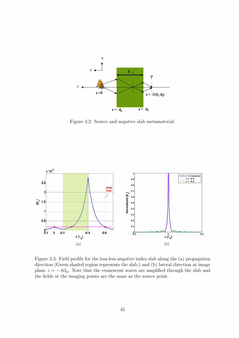
Figure 3.2: Source and negative slab metamaterial.
(a)
−0.5 0 0.50
0.1
0.2
0.3
0.4
0.5
0.6
0.7
0.8
0.9
1
x (λ0)
Nor
mal
ized
|Dz|
z = 0 (source)z = −2 dz = −6 d
(b)
Figure 3.3: Field profile for the loss-less negative index slab along the (a) propagationdirection (Green shaded region represents the slab,) and (b) lateral direction at imageplane z = −.6λp. Note that the evanescent waves are amplified through the slab andthe fields at the imaging points are the same as the source point.
45
In reality because of causality, the left handed materials should be absorbing.
Therefore let us now assume that the slab has some absorption such that n = −1+ ini.
Then the reflection terms, RTM and RTE, in Eq. (3.3) and Eq. (3.4) will contribute
into the calculations. Let us consider a lossy NIM slab with thickness of 4.5d = .45λp
is illuminated by an electric dipole placed at distance d from the first surface (α =
π/6). Fig. 3.4(a) shows the electric field along the slab axis when the loss factor is
γp = .001ωp. In Fig. 3.4(b) the resolution of images of two dipoles (separated .2λ along
the x-direction) at different planes after the slab has been examined. Because of the
decaying profile of the waves in free space the resolution of image goes away by getting
distance from the slab.
To investigate the effect of the loss, it will be suitable to define a transfer function
for the slab in terms of kρ, given as below
T (kρ) =Ez(kρ, kz)|NIM−slab
z=−d2
Ez(kρ, kz)|free−spacez=−d1
. (3.10)
This is the ratio of the field right after the slab to the field at z = −d1 where there is no
slab. Fig. 3.5(a) shows the transfer function for the NIM slab with different material
losses. The slab with smaller loss transfers and amplifies more components in the
evanescent region that results in higher resolution for the image. We also demonstrate
in Fig. 3.5(b) the images of the electric dipole pair for different losses. As obtained,
one can establish higher resolution for smaller loss tangent, such that for damping
factor larger than γp = .01ωp the dipoles can not been separated in the image plane.
3.4 Coupled Surface-Modes Layers
Despite the simple theory for performing a NIM perfect lens, making a bulk material of
NIM with negative permittivity and negative permeability effective materials is a real
challenge. Besides this, due to relatively large thickness of the slab, material loss will
46

(a)
−0.8 −0.6 −0.4 −0.2 0 0.2 0.4 0.6 0.80
0.2
0.4
0.6
0.8
1
x (λ0)
No
rma
lize
d |D
z|
zi = −5.5d
zi = −6d
zi = −7d
zi = −9d
(b)
Figure 3.4: Field profile for the lossy negative index slab of thickness 4.5d = .45λp:(a) propagation direction (Green shaded region represents the slab), and (b) imageperformance at different image planes of a dipole pair separated by .2λ0 (d = .1λp).
0 5 10 15 2010
−15
10−10
10−5
100
105
kρ/k0
| Tra
nsf
er
Fu
nct
ion
|
γp = .001 ω
p
γp = .01 ω
p
γp = .1 ω
p
(a)
−0.8 −0.6 −0.4 −0.2 0 0.2 0.4 0.6 0.80
0.1
0.2
0.3
0.4
0.5
0.6
0.7
0.8
0.9
1
x (λ0)
No
rma
lize
d |D
z|
γp = .001 ω
p
γp = .01 ω
p
γp = .1 ω
p
(b)
Figure 3.5: Effect of loss: (a) transfer function of the slab, and (b) image performanceat the plane z = −.6λp of a dipole pair separated by .2λ0. It can be seen that smallerloss provides higher resolution.
47

considerably degrade the image performance. On the other hand, as the transverse
imaging is the most promising feature of a NIM slab, one can achieve a better practical
subwavelength imaging device (for transverse plane) with the use of coupled layered
surfaces supporting surface waves on their positive-negative boundaries. The positive-
negative layered structures can support surface plasma oscillations (SPO) excited by
evanescent fields. In this section, we will investigate coupled surface wave layers and
compare their performance with the NIM slab.
3.4.1 Analysis of Multiple Thin Film Systems
In general, the presence of surfaces introduces new modes of plasma oscillations in
addition to the bulk mode with different properties and particularly with different
dispersion relations. These modes can be excited by incident electrons, or photons
and can be detected experimentally [57]. To follow the theory for a multiple film
system, we begin with Maxwell’s equations and wish to find solutions which satisfy
Maxwell’s equations with a local current-field relation as follows:
∇.D = 0, (3.11a)
∇.H = 0, (3.11b)
∇.E = −1
c
∂H
∂t, (3.11c)
∇.H =1
c
∂D
∂t, (3.11d)
D = ε(ω)E, (3.11e)
Boundary conditions of continuity of the tangential fields at every boundary should
be applied. Here we are looking for the type of solution corresponds to wave propa-
gation along a direction parallel to the boundary surfaces which separate the different
materials. Here we consider the z axis normal to these surfaces and the x axis is the
direction of wave propagation. Since the magnetic (or TE) waves are purely transverse
48

waves and of no interest to us, we restrict ourselves to the electric (or TM) waves. By
this assumption, there is no y dependence of any of the fields.
The solution for any component of the fields can be represented by the form,
f(x, z, t) = <F (x)ei(ωt−kz) (3.12)
with <k > 0 and =k < 0, so that the wave travels and is attenuated in the positive x
direction. A general solution to 3.11 is a linear combination of the two independent
solutions eKi,mz and e−Ki,mz, where
K2i,m = k2 − ω2εi,m/c2 (3.13)
First, let us examine a single metal-dielectric interface as shown in Fig. 3.6(a). The
solution for Ez is:
Ez = AIeKmz, z < 0 (3.14a)
Ez = AIIe−Kiz, z > 0 (3.14b)
Continuity of the fields across the boundary gives the dispersion relation as,
εiKm + εmKi = 0. (3.15)
The dispersion diagram for an insulator-metal interface when εi = 1, εm = 1−ω2p/ω
2
is plotted in Fig. 3.6(b).
Now, let us investigate the characteristics of a structure constituted from two thin
layers each of them made of a negative permittivity medium. In optics, materials with
negative ε in a limited frequency range are common. The condition for the existence of
a surface plasmon (for p-polarized incident wave) at the surfaces of a layered structure
composed of two ENG layers with thickness dm and separated by d0 in free space (as
49
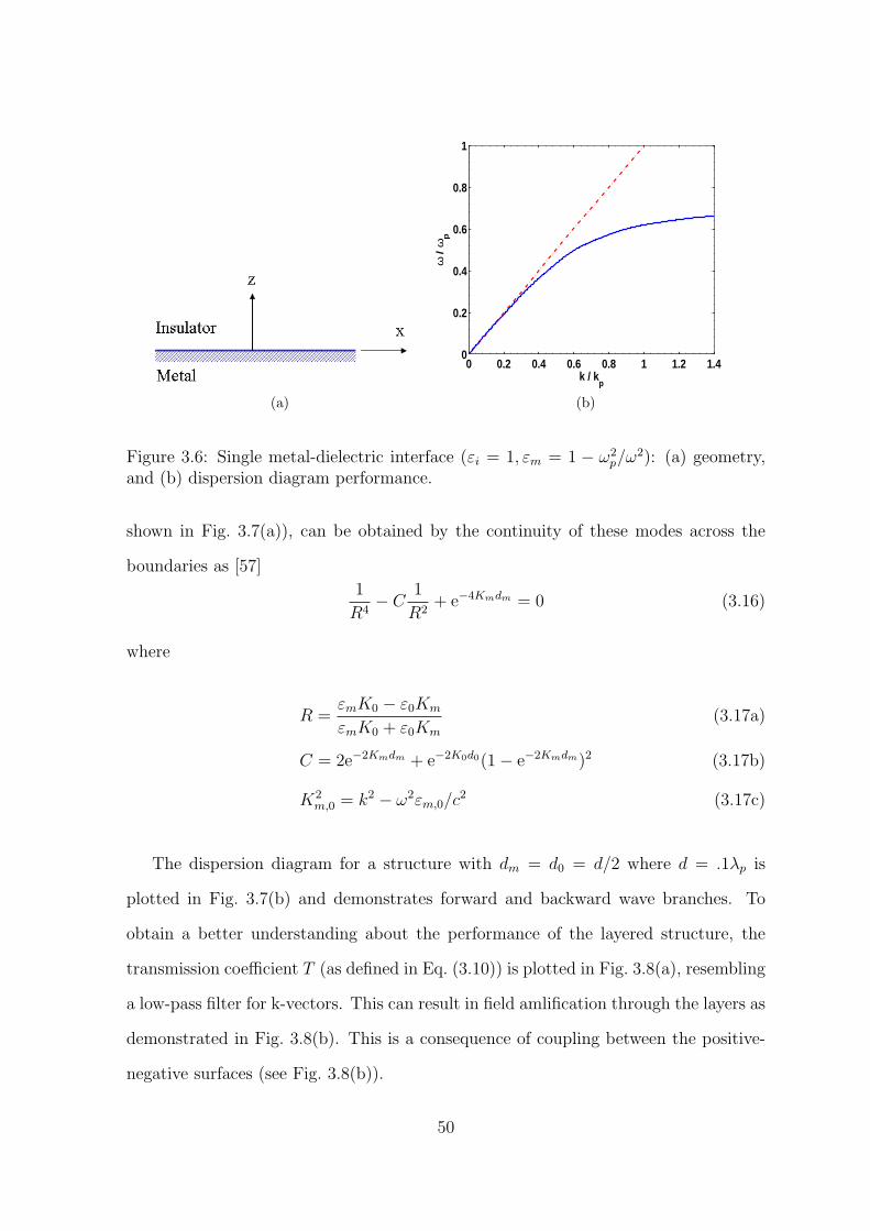
(a)
0 0.2 0.4 0.6 0.8 1 1.2 1.40
0.2
0.4
0.6
0.8
1
k / kp
ω /
ωp
(b)
Figure 3.6: Single metal-dielectric interface (εi = 1, εm = 1 − ω2p/ω
2): (a) geometry,and (b) dispersion diagram performance.
shown in Fig. 3.7(a)), can be obtained by the continuity of these modes across the
boundaries as [57]
1
R4− C
1
R2+ e−4Kmdm = 0 (3.16)
where
R =εmK0 − ε0Km
εmK0 + ε0Km
(3.17a)
C = 2e−2Kmdm + e−2K0d0(1− e−2Kmdm)2 (3.17b)
K2m,0 = k2 − ω2εm,0/c
2 (3.17c)
The dispersion diagram for a structure with dm = d0 = d/2 where d = .1λp is
plotted in Fig. 3.7(b) and demonstrates forward and backward wave branches. To
obtain a better understanding about the performance of the layered structure, the
transmission coefficient T (as defined in Eq. (3.10)) is plotted in Fig. 3.8(a), resembling
a low-pass filter for k-vectors. This can result in field amlification through the layers as
demonstrated in Fig. 3.8(b). This is a consequence of coupling between the positive-
negative surfaces (see Fig. 3.8(b)).
50

The separation between the layers obviously plays an important role to establish
the proper coupling-performance. Hence, one needs to use an optimized separation
between them. This is explored in further details for the transmission coefficient, T,
in Fig. 3.9. As observed, the optimized thickness is d0 = di = .05λp where the effective
ε in transverse plane tends to zero and a smooth transfer function amplifying more k
vectors has been observed.
(a)
0 2 4 6 8 10 12 14 16 180
0.1
0.2
0.3
0.4
0.5
0.6
0.7
0.8
0.9
1
k / kp
ω /
ωp
(b)
Figure 3.7: Two-layer ENG coupled surfaces: (a) geometry, and (b) dispersion diagramperformance when dm = d0 = .05λp. Negative-positive coupled surfaces demonstratethe forward and backward surface wave branches.
Extending the concept of coupled ENG layers to N-layered structure, one can
manipulate the field in a farther distance. This idea has been investigated comprehen-
sively by Ramakrishna et al in [19–21], P. A. Belov et al in [52], and X. Li et al in [53]
for layered periodic structures. Existing TM surface polariton (p-waves) at an inter-
face requires negative dielectric primitivity at one side, whereas the duality supporting
TE surface modes (s-waves) needs negative material permeability. The focus here is
to integrate the ENG layers with the MNG layers making a transverse imaging device
almost independent of the polarization, for instance using alternative ENG and MNG
layers in the structure shown in Fig. 3.1. MNG layers may be utilized by depositing
metallic loop patterns on a coated plasma film or by using coupled ferrite thin-films
51
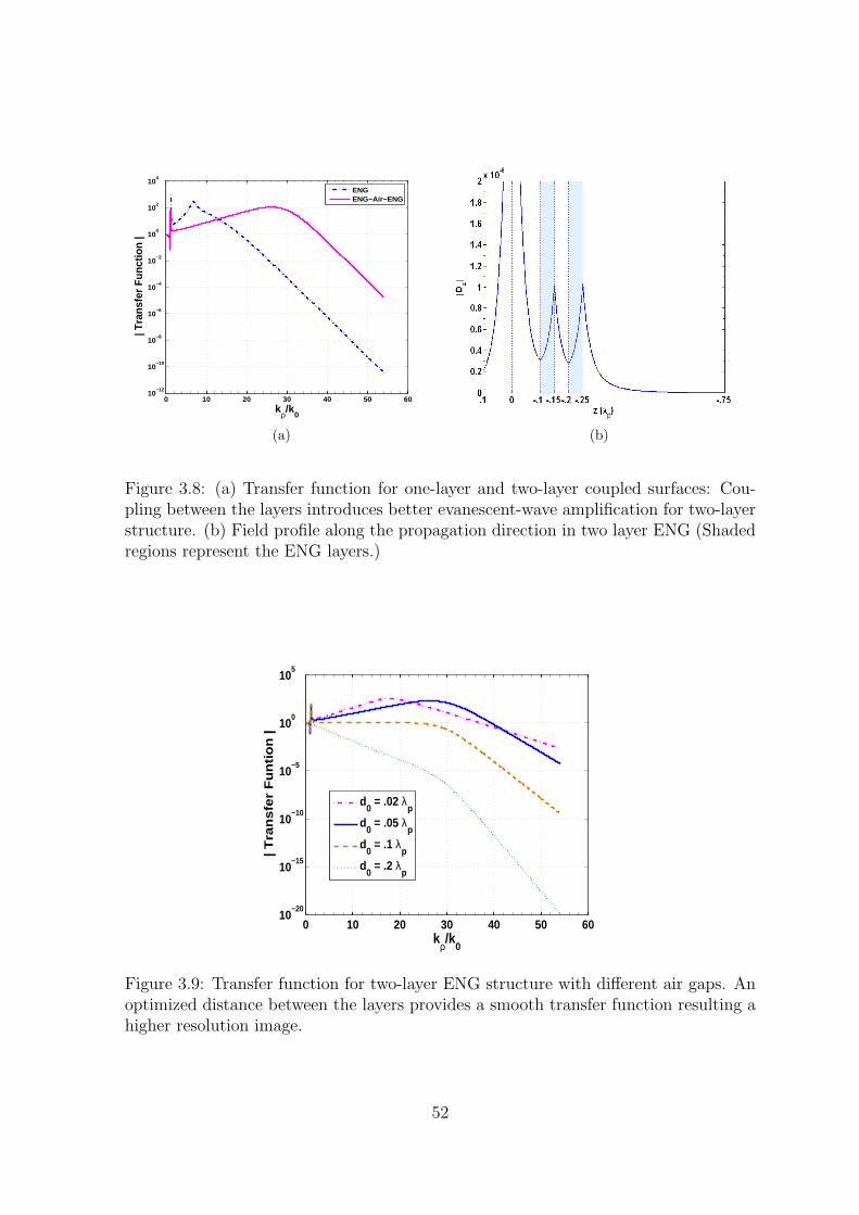
0 10 20 30 40 50 6010
−12
10−10
10−8
10−6
10−4
10−2
100
102
104
kρ/k
0
| Tra
nsfe
r Fun
ctio
n |
ENG ENG−Air−ENG
(a) (b)
Figure 3.8: (a) Transfer function for one-layer and two-layer coupled surfaces: Cou-pling between the layers introduces better evanescent-wave amplification for two-layerstructure. (b) Field profile along the propagation direction in two layer ENG (Shadedregions represent the ENG layers.)
0 10 20 30 40 50 6010
−20
10−15
10−10
10−5
100
105
kρ/k
0
| T
ran
sfe
r F
un
tion
|
d0 = .02 λ
p
d0 = .05 λ
p
d0 = .1 λ
p
d0 = .2 λ
p
Figure 3.9: Transfer function for two-layer ENG structure with different air gaps. Anoptimized distance between the layers provides a smooth transfer function resulting ahigher resolution image.
52
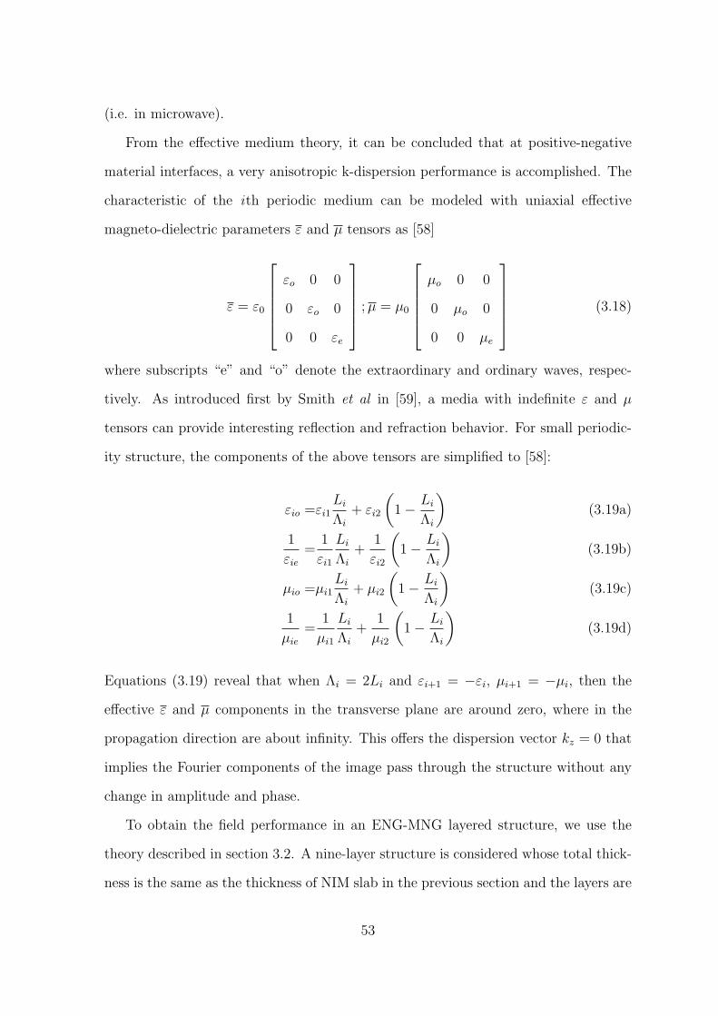
(i.e. in microwave).
From the effective medium theory, it can be concluded that at positive-negative
material interfaces, a very anisotropic k-dispersion performance is accomplished. The
characteristic of the ith periodic medium can be modeled with uniaxial effective
magneto-dielectric parameters ε and µ tensors as [58]
ε = ε0
εo 0 0
0 εo 0
0 0 εe
; µ = µ0
µo 0 0
0 µo 0
0 0 µe
(3.18)
where subscripts “e” and “o” denote the extraordinary and ordinary waves, respec-
tively. As introduced first by Smith et al in [59], a media with indefinite ε and µ
tensors can provide interesting reflection and refraction behavior. For small periodic-
ity structure, the components of the above tensors are simplified to [58]:
εio =εi1Li
Λi
+ εi2
(1− Li
Λi
)(3.19a)
1
εie
=1
εi1
Li
Λi
+1
εi2
(1− Li
Λi
)(3.19b)
µio =µi1Li
Λi
+ µi2
(1− Li
Λi
)(3.19c)
1
µie
=1
µi1
Li
Λi
+1
µi2
(1− Li
Λi
)(3.19d)
Equations (3.19) reveal that when Λi = 2Li and εi+1 = −εi, µi+1 = −µi, then the
effective ε and µ components in the transverse plane are around zero, where in the
propagation direction are about infinity. This offers the dispersion vector kz = 0 that
implies the Fourier components of the image pass through the structure without any
change in amplitude and phase.
To obtain the field performance in an ENG-MNG layered structure, we use the
theory described in section 3.2. A nine-layer structure is considered whose total thick-
ness is the same as the thickness of NIM slab in the previous section and the layers are
53
composed of ENG and MNG materials with loss factor γp = .001ωp, alternatively. The
thickness of each layer is d/2 (d = .1λp) and the structure is illuminated by a dipole
pair (of separation .2λ0) directed along the u direction (α = π/6) in distance d from
the structure (the same as what we used in section 3.3.) Fig. 3.10(a) represents the
electric and magnetic field distributions along the propagation direction (at ρ = .001λp
and φ = π/4). As expected, the performance for both polarizations is the same and
the image components are transferred successfully providing high-performance sub-
wavelength resolution. The field is amplified inside the layers alternatively and arrives
to the image plane. In Fig. 3.10(b) the image at different planes after the structure is
investigated. Comparing this figure with Fig. 3.4(b), it can be observed that the lay-
ered structure has a better resolution due to the larger enhancement in the k-vectors.
However, since the value of the field at the exiting surface of the layered material is
smaller than that of the NIM slab (for this specific γp), the image reconstruction for
the layered structure degrades more as the distance from the structure output surface
is increased.
However, if the material loss is increased the story is different. Fig. 3.11 demon-
strates the image of the pair of dipoles placed at distance d from the layered structure
for different material losses. The image is observed at z = −6d. As observed, the
layered composite can work successfully up to higher losses around γp = .15ωp and
still can separate the images of two sources, whereas the NIM slab is more sensitive
to the material loss. Basically, the NIM slab for losses larger than γp = .01ωp is un-
able to reconstruct the image (see Fig. 3.5(b)). The large loss of the thick NIM slab
does not allow enough amplification inside the structure where the thin thicknesses of
the positive-negative alternative layered structure allow successful tunneling inside the
medium. By increasing the number of layers the image can be transferred to longer
distances. This behavior is discussed as canalization in the earlier papers [19–21, 52]
for the periodic layered structures.
54

(a)
−0.8 −0.6 −0.4 −0.2 0 0.2 0.4 0.60
0.2
0.4
0.6
0.8
1
x (λ0)
Nor
mal
ized
|Dz|
zi = −5.5d
zi = −6d
zi = −7d
zi = −9d
(b)
Figure 3.10: N-layered ENG-MNG composite (N=9): (a) the electric and magneticfield profiles along the Propagation direction (Blue-shaded layers represent ENG andpink-shaded layers are MNG,) and (b) imaging performance at different planes (d =.1λp).
55

−0.8 −0.6 −0.4 −0.2 0 0.2 0.4 0.60
0.1
0.2
0.3
0.4
0.5
0.6
0.7
0.8
0.9
1
x (λ0)
Nor
mal
ized
|Dz|
γp = .001 ω
p
γp = .01 ω
p
γp = .1 ω
p
γp = .15 ω
p
γp = ω
p
Figure 3.11: Imaging performance at plane z = −.6λp for different material losses.Comparing Fig. 3.11 to Fig. 3.5(b) shows that the layered structure has a betterperformance than the NIM slab for higher material losses.
3.5 FDTD Numerical Analysis of Finite-Size Struc-
ture
In this section, a Finite Difference Time Domain (FDTD) technique is applied to
characterize the layered composite that has finite-size in the transverse directions. Two
ENG and two MNG layers made of Drude permittivity and Lorentzian permeability
materials, respectively (as defined in Eq. (3.8)) with thickness of d/2 = .05λp and
loss factor γp = .001ωp are stacked alternatively along the z. At operating frequency
ω20 = .5ω2
p, the permittivity of ENG layers and permeability of MNG layers are around
-1 and the slab size in transverse plane is 1.5λ0 × 1.5λ0. An electrical dipole source
making angle π/6 with respect to the z axis is illuminating the structure. Fig. 3.12
represents the electric and magnetic field distributions along the propagation direction
inside the layers. The growth-attenuation behavior of the field is in agreement with
the results obtained from the theory. Fig. 3.13 represents the field distribution along
the transverse direction and for comparison, the field performance when there is no
56
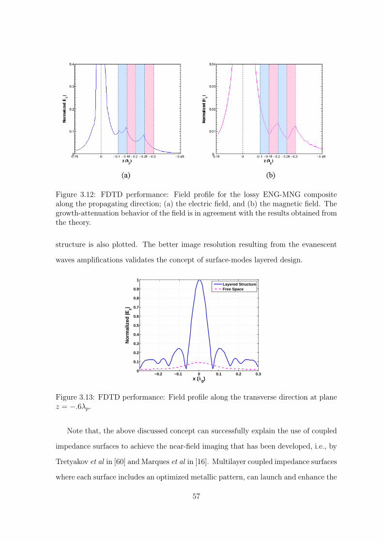
Figure 3.12: FDTD performance: Field profile for the lossy ENG-MNG compositealong the propagating direction; (a) the electric field, and (b) the magnetic field. Thegrowth-attenuation behavior of the field is in agreement with the results obtained fromthe theory.
structure is also plotted. The better image resolution resulting from the evanescent
waves amplifications validates the concept of surface-modes layered design.
−0.2 −0.1 0 0.1 0.2 0.30
0.1
0.2
0.3
0.4
0.5
0.6
0.7
0.8
0.9
1
x (λ0)
Nor
mal
ized
|Ez|
Layered StructureFree Space
Figure 3.13: FDTD performance: Field profile along the transverse direction at planez = −.6λp.
Note that, the above discussed concept can successfully explain the use of coupled
impedance surfaces to achieve the near-field imaging that has been developed, i.e., by
Tretyakov et al in [60] and Marques et al in [16]. Multilayer coupled impedance surfaces
where each surface includes an optimized metallic pattern, can launch and enhance the
57
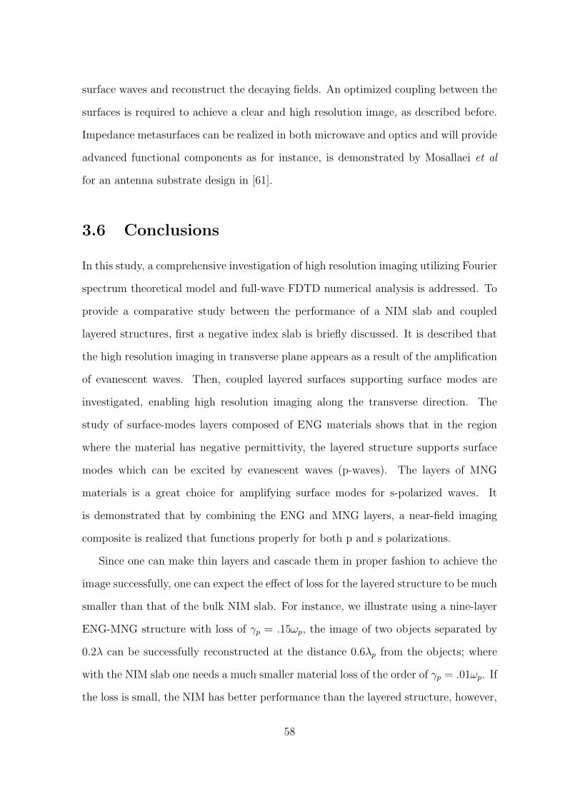
surface waves and reconstruct the decaying fields. An optimized coupling between the
surfaces is required to achieve a clear and high resolution image, as described before.
Impedance metasurfaces can be realized in both microwave and optics and will provide
advanced functional components as for instance, is demonstrated by Mosallaei et al
for an antenna substrate design in [61].
3.6 Conclusions
In this study, a comprehensive investigation of high resolution imaging utilizing Fourier
spectrum theoretical model and full-wave FDTD numerical analysis is addressed. To
provide a comparative study between the performance of a NIM slab and coupled
layered structures, first a negative index slab is briefly discussed. It is described that
the high resolution imaging in transverse plane appears as a result of the amplification
of evanescent waves. Then, coupled layered surfaces supporting surface modes are
investigated, enabling high resolution imaging along the transverse direction. The
study of surface-modes layers composed of ENG materials shows that in the region
where the material has negative permittivity, the layered structure supports surface
modes which can be excited by evanescent waves (p-waves). The layers of MNG
materials is a great choice for amplifying surface modes for s-polarized waves. It
is demonstrated that by combining the ENG and MNG layers, a near-field imaging
composite is realized that functions properly for both p and s polarizations.
Since one can make thin layers and cascade them in proper fashion to achieve the
image successfully, one can expect the effect of loss for the layered structure to be much
smaller than that of the bulk NIM slab. For instance, we illustrate using a nine-layer
ENG-MNG structure with loss of γp = .15ωp, the image of two objects separated by
0.2λ can be successfully reconstructed at the distance 0.6λp from the objects; where
with the NIM slab one needs a much smaller material loss of the order of γp = .01ωp. If
the loss is small, the NIM has better performance than the layered structure, however,
58

in a realistic system with reasonable large loss, the layered structure seems to be more
promising.
The coupled layers of ENG and MNG structures may be created with the use of
metallic patterns. It must also be highlighted that increasing the number of layers will
allow a high performance lateral imaging in a longer distance from the object.
59
Chapter 4
Ellipsoidal Metamaterial
Subwavelength Radiator
4.1 Introduction
Smaller physical size, wider bandwidth and higher radiation efficiency are three de-
sirable characteristics of antennas integrated into communication systems. In recent
years, considerable efforts have been devoted towards antenna miniaturization. Funda-
mentally, the ability of any antenna to radiate effectively depends on ka (where k is the
wave number and a is the radius of the smallest sphere enclosing the antenna) [62, 63].
According to Chu [63], the lower bound on the quality factor (Q) of an electrically
small electric or magnetic dipole antenna is inversely related to the radius of the small-
est sphere that can surround it by the formula QChu = 1/(ka)3+1/(ka); so the smaller
the radius, the higher the Q and the narrower the bandwidth. The challenge is to make
the physical size of the antenna as small as possible along with achieving a wideband
impedance characteristic (Q values close to the lower-bound). Best et al. presented
a comprehensive study in [64] for achieving small antennas with low Q performance
with the use of novel topologies, such as spherical or cylindrical folded helix antennas.
Quality factor as low as 1.5 times of the Chu limit was illustrated. Recently, there have
60

been some efforts to produce wideband electrically small resonant antennas by utilizing
negative parameters materials [65–67]. Stuart et al. in [65] excited an epsilon negative
(ENG) sphere with a dipole feed to produce the appropriate polarization required for
the resonance performance. They demonstrated that one can achieve an electrically
small antenna by operating the spherical radiator in a frequency that corresponds to
the region εr = −2. The sphere-shaped structures offer wideband performance close
to the Chu limit. Ziolkowski et al. have also demonstrated other novel small antenna
designs utilizing combinations of epsilon negative (ENG) and mu negative (MNG) or
double negative (DNG) metamaterials [67]. The focus of this work is on study of small
antennas realized by unique materials.
Practically, it is very useful to investigate the effect of the structural shape of the
material of the antenna on the resonant frequency and Q-factor. For example, can
a slab or a long rod of negative permittivity material also radiate efficiently? If so,
what would be the resonant frequencies and associated material indices? How close
would the Q be to the lower bound? The objectives in this study are to investigate
the resonance radiation of metamaterial-based eccentrically shaped structures with
particular emphasis on the bandwidth limitations or quality factors for the antennas.
Thin disks and long rods, as well as the ellipsoids, will be the special cases that allow
us to address the above questions. To simplify the problem, it is assumed that the size
of the antenna-proper is much smaller than the wavelength in both free-space and in
the material. Hence, the time-harmonic quasi-static approximation can be applied to
successfully formulate the problem and predict the physical parameters of the antenna.
A full-wave numerical technique (using CST STUDIO SUITE 2009 [68]) is applied to
comprehensively model the structure and validate the derived theory. We demonstrate
that a volume of negative permittivity material placed on a ground plane and fed by
a coaxial transmission line can produce a small antenna whose operating frequency
depends on material properties and the height to width ratio of the volume. The Q-
factor of the different shaped radiators are numerically studied and compared to the
61

Figure 4.1: The geometry of ellipsoid with semi-axes ax, ay and az
calculated values based on the reported equations in the recent literatures [69–75].
4.2 Resonance Formulation
Fig. 4.1 shows the geometry of an ellipsoid with semi-axes ax, ay, and az located in free-
space and illuminated by an arbitrary polarized electric field E0 = xE0x + yE0y + zE0z.
It is assumed that the ellipsoid has a material permittivity of ε, and a size which
is much smaller than the free-space wavelength (ax, ay, az ¿ λ). A rigorous static
analysis gives the field inside the ellipsoid as [76, 77],
Eint = xE0x[1− (εr − 1)Nx
1 + (εr − 1)Nx
]+ yE0y[1− (εr − 1)Ny
1 + (εr − 1)Ny
]+ zE0z[1− (εr − 1)Nz
1 + (εr − 1)Nz
],
(4.1)
where Ni(i = x, y, z) are depolarization factors determined from
Ni =axayaz
2
∫ ∞
0
ds
(s + a2i )
√(s + a2
x)(s + a2y)(s + a2
z)(4.2)
As can be seen, the depolarization factors Ni play a critical role in determining
the induced electric field. Note that if the applied electric field is initially uniform,
the resultant field within the ellipsoid is also uniform. Another observation is that the
polarization of the induced field can, in general, be different from that of the applied
field.
62
The three depolarization factors for any ellipsoid satisfy
Nx + Ny + Nz = 1 (4.3)
A sphere has three depolarization factors, each equal to 1/3, and the internal field
is aligned with the applied field, either in the same or opposite direction. Other
special cases are an oblate spheroid with ax = ay > az, and a prolate spheroid with
ax > ay = az. Closed-form expressions for the integral (4.2) can be derived for these
cases. For oblate spheroids we have [77],
Nz =1 + e2
e3(e− tan−1(e)) (4.4a)
Nx = Ny =1
2(1−Nz) (4.4b)
where the eccentricity is e =√
a2x/a
2z − 1. For prolate spheroids we have,
Nx =1− e2
2e3(ln
1 + e
1− e− 2e) (4.5a)
Ny = Nz =1
2(1−Nx) (4.5b)
where e =√
1− a2x/a
2z. The practical utility of the spheroidal cases lies in the oblate
spheroid degenerating into a flat disk as az becomes very small (e → ∞); and the
prolate spheroid approaching a rod-shaped structure as az becomes very large (e → 1).
To investigate some of the important physical implications of Eq. (4.1), consider
a metamaterial ellipsoid located in free-space under the influence of a +z-polarized
electric field. For the spherical geometry case, the internal field Eint simplifies to,
Eint = zE0z(1− εr − 1
εr + 2) (4.6)
When the permittivity of the sphere, εr, is larger than the permittivity of the free
63
space in which the sphere is assumed to reside, the sphere is depolarized along the -z
direction, and the total internal field reduces as the permittivity is increased. However,
for the sphere permittivity below the outside material value (vacuum), the sphere can
be polarized along the excitation (+z direction), and near εr = −2, one can establish
a resonance with strong field intensity inside the sphere (independent of the size of
sphere). Below εr = −2, the polarization of induced field switches again from +z to
again -z, and as the permittivity becomes very large negatively, the induced field tends
to cancel the external field producing nearly a zero total field inside the sphere.
Changing the shape of the ellipsoid has some interesting effects on the resonance
performance. For instance, if the geometry deforms from the sphere with polarization
factors (1/3,1/3,1/3) into a flat disk with those of (0,0,1), Eq. (4.1), shows that the
internal field is simplified to Eint = zE0z(1/εr). Thus, the thin disk becomes resonant
at around εr = 0. Hence, altering the antenna shape from that of a sphere to a disk
will shift the required permittivity for resonance from εr = −2 to εr = 0. It is also
found from Eq. (4.1) that by changing the shape of the antenna from a sphere to an
increasingly long rod (along z), the permittivity required to produce a resonance shifts
from εr = −2 to εr → −∞.
4.3 Calculation of the Lower Bounds on Q
So far, we have concentrated on the resonance characteristics of the metamaterial-
based ellipsoid. The bandwidth, which is inversely proportional to the Q of an an-
tenna [69], is another important consideration for practical electrically small antennas.
The concept of lower bounds on the Q of electrically small antennas was first intro-
duced by Wheeler [62] and Chu [63]. According to Chu [63], the minimum Q that one
can achieve for an antenna confined to a spherical volume of radius a obeys the rela-
tionship QChu = 1/(ka)3 + 1/(ka), ka ¿ 1, which means that decreasing the electrical
size of the resonator increases its Q and narrows its bandwidth. Recently, attention
64
has been drawn to the subject of the lower bounds on the Q for antennas confined to
arbitrarily shaped volumes. Gustafsson et al. determined physical bounds on anten-
nas of arbitrary shape [71, 72] using an approach based on fundamental principles of
causality, time-translated invariance, and reciprocity applied to a general set of linear
constitutive relations via a sum rule [72]. More recently, Yaghjian et al. have shown
that the minimum possible Q for an electrically small dipole antenna confined to an
arbitrary volume V will be the Q of a PEC scatterer filling V subject to a uniform
incident electric field. This lower bound Q can be expressed in terms of the direction
of the electric dipole moment (p = p/|p|), and the electrostatic polarizability dyadic
αe of the PEC volume V [73, 74],
Qed,lb =6π
k3
(p.α−1
e .p− V |α−1e .p|2) (4.7)
which for a principal direction of the volume V , becomes
Qed,lb =6π
k3αp
(1− V/αp
)(4.8)
Equations (4.7) and (4.8) apply to linear electric or magnetic dipole antennas whose
exciting sources can be both electric currents and magnetic currents (polarization M)
outside the “antenna-proper.” For electric-dipole antennas confined to an electrically
small volume V excited by electric-currents only, such as the antennas in this study,
the lower bound on the quality factor reduces to [73, 74],
Qeced,lb =
6π
k3p.α−1
e .p (4.9)
which for a principal direction of the volume V , becomes
Qeced,lb =
6π
k3αp
(4.10)
It is often convenient to re-express αp as fsV , where fs is a dimensionless “shape
65
factor.”
In the following sections, we numerically compute the actual Q for simulated spher-
ical, circular-cylindrical-disk, and circular-cylindrical-rod antennas, and then compare
these values of Q to the Q lower bounds given in Eq. (4.10) determined from the shape
factors for these antennas.
4.4 Performance Analysis of ENG Antennas
To provide physical insight into these metamaterial-based antennas, their detailed
performance characteristics will now be investigated. To form an antenna element,
the resonator must be coupled to a transmission line. For each antenna on a ground
plane, (half sphere, half disk, and half rod), the antenna is fed by a 50 Ohm coaxial
transmission line with a small monopole stub. The dimension of the stub is varied in
order to find the optimum impedance match. It is assumed that the metamaterial of
the antenna has a Drude-dispersive permittivity satisfying,
ε(ω) = ε0
(1− ω2
e
ω(ω + iγe)
)(4.11)
where ωe = 2π×4×109(rad/s) is the bulk resonant frequency of the material, and the
damping factor γe = 0.001ωe determines the loss. The Drude permittivity is plotted
in Fig. 4.2. This Drude metamaterial may be constructed in microwave frequencies
with the use of array of subwavelength metallic wires [78], although it features a larger
frequency dispersion than a regular wire medium affecting the desired bandwidth (in
optics, a plasmonic metal can simply provide the Drude dispersive property).
All simulations are performed with the finite integration method using CST [68]
with an absorbing boundary condition implemented at a distance of one wavelength
from the antenna element.
66

0 1 2 3 4 5−20
−15
−10
−5
0
5
10
Rel
ativ
e P
erm
ittiv
ity
Frequency (GHz)
Real−Imaginary
Figure 4.2: Characteristics of the Drude permittivity material.
4.4.1 Spherical Radiator
Fig. 4.3 depicts the geometry of a hemisphere located on a ground plane. For a
large ground plane, the hemisphere can be considered a sphere for modeling purposes.
A probe-feed is used to excite the resonant mode of the sphere. Since the sphere
is assumed to have a very small radius (a = 7.5 mm), compared to wavelength, the
above quasi-static discussions can be applied. The optimum stub length and radius are
determined through simulation to be 4.5 mm and 1.2 mm, respectively. The antenna
input impedance and return loss versus frequency are shown in Fig. 4.4. A resonance
near the frequency which is associated with εr = −2 is determined and a −10dB
impedance matching at f = 2.36 GHz is obtained by tuning the stub (ka = 0.37).
This demonstrates good agreement with the quasi-static prediction for the resonance
frequency at εr = −2. The operating wavelength is 127.1 mm and the stub length
is about λ/29. The diameter of the sphere radiator at the operating frequency is
about λ/8.5. The resonant frequency of the antenna indeed corresponds to that of
the fundamental mode of the negative permittivity sphere explained in the previous
section.
To better understand the physical performance of the sphere, the electric field at
67

Figure 4.3: The geometry of the hemisphere radiator constructed from the Drudedielectric medium.
the resonant frequency is plotted in Fig. 4.5(a) (line-fields at some arbitrary moment in
the y-z plane). Note that the normal component of the electric field has different signs
inside and outside the sphere due to the negative permittivity value. The negative
permittivity sphere acts like an inductor which is in parallel with the dipole-feed
capacitor. The dipole-feed capacitor can be used for tuning the antenna resonant
characteristic. The antenna radiation pattern shown in Fig. 4.5(b) is that of an electric
dipole, as expected from the field distribution inside the radiator. The bandwidth and
Q of the antenna are also determined based on equation (96) of [73]. The 3dB matched
VSWR bandwidth is 6.4% at the operating frequency; therefore, the Q corresponding
to the half-power VSWR bandwidth yields a value of about 31.25 at the resonant
frequency of the antenna. Fig. 4.4(b) shows return loss versus frequency for the same
antenna described above with the lossless material. The length of the stub is tuned
to be 4.4 mm to improve the impedance matching performance. The Q (for 100%
efficiency) corresponding to half-power VSWR bandwidth (5.9%) yields a value of
around 33.9 at the resonant frequency of the antenna, which is about 1.51 times the
Chu lower bound for an antenna with ka = 0.37 (QChu = 22.4). Equation (4.10) also
predicts a Q of 1.5 times the Chu lower bound for a sphere which has a polarizability
of αe = 4πa3 (fs = 3).
Since the material parameters include loss, a reduction in efficiency is expected.
68

The radiation efficiency is plotted versus frequency in Fig. 4.4(b). As observed, near
the operating bandwidth, the efficiency is nearly flat at a value of about 92%.
2 2.1 2.2 2.3 2.4 2.52.5−400
−200
0
200
400
600
800
1000
Frequency (GHz)
Impe
danc
e (O
hms)
ResistanceReactance
(a)
2 2.1 2.2 2.3 2.4 2.52.5−30
−25
−20
−15
−10
−5
0
Frequency (GHz)R
etu
rn L
oss
(d
B)
0
20
40
60
80
100
Ra
dia
tion
Effic
ien
cy (
%)
with lossno loss
(b)
Figure 4.4: The performance of the hemisphere structure: (a) input impedance, and(b) return loss and radiation efficiency.
4.4.2 Circular Cylindrical Disk Radiator
From a practical point of view, one may be interested in the resonance performance
of an ENG disk instead of the sphere, the disk being easier to construct. Fig. 4.6
shows the geometry of a disk with radius of R = 5.31 mm and height of h = 1.77
mm (R/h = 3) located above a ground plane. The disk is composed of the Drude
medium given in (4.11). Using equations (4.1) and (4.4), a resonance with strong field
intensity inside the disk is expected to occur at f = 3.19 GHz, which corresponds to
εr = −0.57 based on the Drude material characteristics. (At this frequency, the ka
of the smallest circumscribing sphere is 0.37.) Here the radius and height of the disk
are approximated by the major and minor axes of an ellipse, respectively. To obtain
an impedance match, the inner stub is given a radius of 0.55 mm and a length of
1.5 mm. The resonance performance with −10dB impedance matching near f = 3.42
GHz is obtained and shown in Fig. 4.7, and the electric field is shown in Fig. 4.8. A
69

(a) (b)
Figure 4.5: Radiator performance at the resonant frequency, f = 2.36 GHz: (a) E-field pattern in the y-z plane. Note to the depolarized fields inside the sphere, and (b)radiation pattern. It presents a dipole mode of the antenna as expected of the fielddistribution inside the radiator.
uniform depolarized field pattern inside the disk is established. It is worth mentioning
that since the normal component Dn of the displacement on the surface of the disk is
continuous, a small value of permittivity inside the radiator which is the case for this
resonant disk produces a very strong internal electric field. The 3dB matched VSWR
bandwidth is about 0.88%.
The lossless case of a 1.5 mm stub with a radius of 0.45 mm is also shown in
Fig. 4.7(b). The 3dB matched VSWR bandwidth of 0.71% at the resonant frequency
gives a Q equal to 281.3. The Q of the disk is much higher than that of a circumscribing
sphere because the disk occupies a much smaller volume than its circumscribing sphere.
To calculate the Q factor of the disk based on Eq. (4.10), one needs to calculate
αe first, which can be estimated from the shape factor fs that computes to 1.97 for a
disk with height to width ratio of 1/3 [75]. From (4.10), this shape factor gives a Q
lower bound of 83.3. Our numerical calculation for the Q of the disk (Q = 281.3) is
much higher than the theoretical lower-bound prediction. This can be mainly because
of the antenna shape and the type of its excitation. In other words, since the electric
flux density Dn must be continuous on the surface of the disk, and since the antenna
goes to the resonance for ε close to zero, the field concentration inside the disk must
70
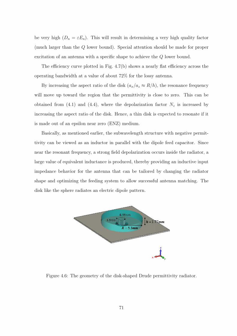
be very high (Dn = εEn). This will result in determining a very high quality factor
(much larger than the Q lower bound). Special attention should be made for proper
excitation of an antenna with a specific shape to achieve the Q lower bound.
The efficiency curve plotted in Fig. 4.7(b) shows a nearly flat efficiency across the
operating bandwidth at a value of about 72% for the lossy antenna.
By increasing the aspect ratio of the disk (ax/az ≈ R/h), the resonance frequency
will move up toward the region that the permittivity is close to zero. This can be
obtained from (4.1) and (4.4), where the depolarization factor Nz is increased by
increasing the aspect ratio of the disk. Hence, a thin disk is expected to resonate if it
is made out of an epsilon near zero (ENZ) medium.
Basically, as mentioned earlier, the subwavelength structure with negative permit-
tivity can be viewed as an inductor in parallel with the dipole feed capacitor. Since
near the resonant frequency, a strong field depolarization occurs inside the radiator, a
large value of equivalent inductance is produced, thereby providing an inductive input
impedance behavior for the antenna that can be tailored by changing the radiator
shape and optimizing the feeding system to allow successful antenna matching. The
disk like the sphere radiates an electric dipole pattern.
Figure 4.6: The geometry of the disk-shaped Drude permittivity radiator.
71

3.2 3.3 3.4 3.5−4000
−2000
0
2000
4000
6000
Frequency (GHz)
Imp
ed
an
ce (
Oh
ms)
ResistanceReactance
(a)
3.2 3.25 3.3 3.35 3.4 3.45 3.5−30
−25
−20
−15
−10
−5
0
Frequency (GHz)
Re
turn
Lo
ss (
dB
)
0
20
40
60
80
100
Ra
dia
tion
Effic
ien
cy (
%)
with lossno loss
(b)
Figure 4.7: The performance of the disk-shaped radiator: (a) input impedance, and(b) return loss and radiation efficiency.
Figure 4.8: E-field pattern in the y-z plane for the disk at the resonant frequency,f = 3.42 GHz. Note to the strong field depolarization inside the disk proving largeinductive behavior.
72

Figure 4.9: The geometry of the rod-shaped Drude permittivity radiator.
4.4.3 Circular Cylindrical Rod Radiator
The performance of a Drude-material rod-shaped antenna is considered next. The
geometry of a long rod with radius R = 4.23 mm and height h = 12.69 mm located
above a ground plane is shown in Fig. 4.9. Using quasi-static equations (4.1) and (4.5),
a resonance with strong field intensity inside the rod is predicted to occur at f = 1.32
GHz which corresponds to εr = −8.199 at the same ka of 0.37. (The height and
radius of the rod in this calculation are that of an ellipse with these major and minor
axes, respectively.) By optimizing the stub to have a radius of 0.5 mm and length
of 2.35 mm, the antenna is matched to 50 ohm near f = 1.13 GHz . The numerical
performance obtained by CST is illustrated in Figs. 4.10 and 4.11. The 3dB matched
VSWR bandwidth is 2.88%. The return loss for the lossless case of a 2.05 mm stub
(shown in Fig. 10(b)) gives the bandwidth of 2.16% corresponding to a Q of 92.4,
about 2.6 times the Chu lower bound (QChu = 35.5) for an antenna with ka = 0.314
where a is the radius of the smallest sphere enclosing the rod. The lower bound for the
actual rod volume can be found from (4.10) to be 92 after using the computed shape
factor of 10.8 for this rod with height/width = 3 [75]. As observed, the lower-bound
value is close to the actual simulated value for this rod antenna. The internal field is
73
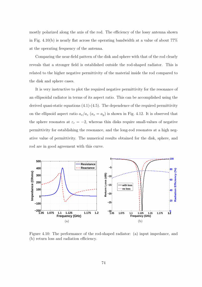
mostly polarized along the axis of the rod. The efficiency of the lossy antenna shown
in Fig. 4.10(b) is nearly flat across the operating bandwidth at a value of about 77%
at the operating frequency of the antenna.
Comparing the near-field pattern of the disk and sphere with that of the rod clearly
reveals that a stronger field is established outside the rod-shaped radiator. This is
related to the higher negative permittivity of the material inside the rod compared to
the disk and sphere cases.
It is very instructive to plot the required negative permittivity for the resonance of
an ellipsoidal radiator in terms of its aspect ratio. This can be accomplished using the
derived quasi-static equations (4.1)-(4.5). The dependence of the required permittivity
on the ellipsoid aspect ratio ax/az (ax = ay) is shown in Fig. 4.12. It is observed that
the sphere resonates at εr = −2, whereas thin disks require small-values of negative
permittivity for establishing the resonance, and the long-rod resonates at a high neg-
ative value of permittivity. The numerical results obtained for the disk, sphere, and
rod are in good agreement with this curve.
1.05 1.075 1.1 1.125 1.175 1.2−200
−100
0
100
200
300
400
500
Frequency (GHz)
Imp
ed
an
ce (
Oh
ms)
ResistanceReactance
(a)
1.05 1.075 1.1 1.125 1.15 1.175 1.21.2−30
−25
−20
−15
−10
−5
0
Frequency (GHz)
Re
turn
Lo
ss (
dB
)
0
20
40
60
80
100
Ra
dia
tion
Effic
ien
cy (
%)
with lossno loss
(b)
Figure 4.10: The performance of the rod-shaped radiator: (a) input impedance, and(b) return loss and radiation efficiency.
74
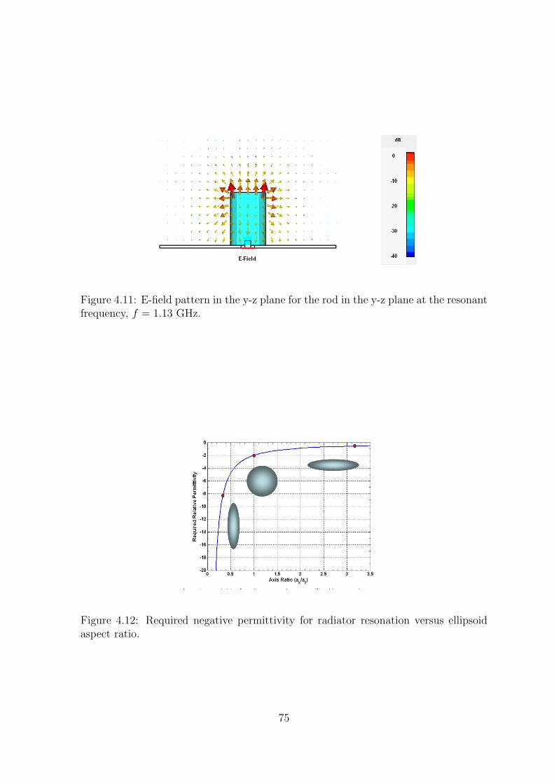
Figure 4.11: E-field pattern in the y-z plane for the rod in the y-z plane at the resonantfrequency, f = 1.13 GHz.
Figure 4.12: Required negative permittivity for radiator resonation versus ellipsoidaspect ratio.
75

4.5 MNG Slab Resonance Radiator
So far, the concept of subwavelength radiators has been highlighted with the use of
negative permittivity materials. Basically, the major practical issue is that one cannot
achieve a material with negative permittivity in microwave region. Magnetic materials
are more promising in this regard[10]. In fact, one can use a self-biased hexaferrite in
GHz spectrum with negative permeability feature above its resonance, to establish a
small-size radiator. Fig. 4.13(a) depicts the geometry of a subwavelength rectangular
slab made of a magnetic material with Lorentzian permeability function
µ(ω) = µ0(1− κ2 ω2
ω2 − ω2h + i2γhω
), (4.12)
with magnetic resonant frequency ωh = 2π × 2 × 109(rad/s), damping factor γh =
0.001ωh, and coupling coefficient κ = 0.707. The characteristic of medium is plotted
in Fig. 4.9(b). The slab is located above a ground plane containing an aperture to
couple the field from a microstrip line to the system.
(a) (b)
Figure 4.13: Slab radiator constructed from the Lorentzian magnetic medium given byEq. (4.12): (a) the geometry, and (b) Lorentzian permeability behavior. The groundplane is finite with size 22.5mm× 30mm.
The equivalent magnetic current of the aperture excitation can tune the capacitive
76
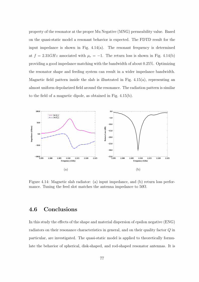
property of the resonator at the proper Mu Negative (MNG) permeability value. Based
on the quasi-static model a resonant behavior is expected. The FDTD result for the
input impedance is shown in Fig. 4.14(a). The resonant frequency is determined
at f = 2.31GHz associated with µr = −1. The return loss is shown in Fig. 4.14(b)
providing a good impedance matching with the bandwidth of about 0.25%. Optimizing
the resonator shape and feeding system can result in a wider impedance bandwidth.
Magnetic field pattern inside the slab is illustrated in Fig. 4.15(a), representing an
almost uniform depolarized field around the resonance. The radiation pattern is similar
to the field of a magnetic dipole, as obtained in Fig. 4.15(b).
2.295 2.300 2.305 2.310 2.315 2.320 2.325Frequency (GHz)
−100.0
−50.0
0.0
50.0
100.0
Impe
danc
e (O
hms)
Re [Zin]Im [Z in]
(a)
2.295 2.300 2.305 2.310 2.315 2.320 2.325Frequency (GHz)
−35.0
−30.0
−25.0
−20.0
−15.0
−10.0
−5.0
0.0
Ret
urn
Loss
(dB
)
(b)
Figure 4.14: Magnetic slab radiator: (a) input impedance, and (b) return loss perfor-mance. Tuning the feed slot matches the antenna impedance to 50Ω.
4.6 Conclusions
In this study the effects of the shape and material dispersion of epsilon negative (ENG)
radiators on their resonance characteristics in general, and on their quality factor Q in
particular, are investigated. The quasi-static model is applied to theoretically formu-
late the behavior of spherical, disk-shaped, and rod-shaped resonator antennas. It is
77

(a) (b)
Figure 4.15: (a) Near field in xy-plane, and (b) radiation pattern of the magnetic slabradiator. Note to the H-field depolarization. The slab generates magnetic dipole moderadiation performance.
demonstrated that for a spherical geometry the resonance occurs at εr = −2, whereas
a thin disk resonates at smaller negative permittivity and a long rod resonates at a
larger negative permittivity. The full-wave numerical technique using CST software is
applied to fully characterize the antenna radiator and match its input impedance to its
feed line using a monopole stub. Numerically simulated values of the quality factor Q
are compared with the Q lower bounds for these different shaped radiators calculated
from recently published formulas for the Q lower bounds of electric-dipole antennas
confined to an arbitrarily shaped volume. The simulated Qs for the ENG sphere and
rod are almost the same as the theoretical calculation, while that for the disk is about
3.38 times of the calculated value (equation (4.10)). Considering the type of electric
dipole excitation, the sphere and rod use the best opportunity (regarding the excita-
tion and the use of volume) to offer the closest Q to the lower bounds. And obviously,
the sphere provides the minimum Q between all these configurations, although it has
a Q of 1.5 times of the Chu lower bound. The Chu lower bound may be achieved by
an antenna design with proper excitations of both electric and magnetic polarizations
78

and optimal configurations.
We also demonstrate radiation characteristics of small resonators made of negative
permeability materials. It is illustrated how a resonator composed of negative per-
meability medium can successfully establish a small antenna element. The obtained
observations may provide road maps for the future design of metamaterial-based sub-
wavelength antennas.
79
Chapter 5
Optical Reflectarray Nanoantenna
5.1 Introduction
Reflectarray antennas are a class of antennas that combine the features of reflectors
and phased arrays providing a directive beam in a desired scanned angle. The most
important advantages of reflect arrays over phased arrays are the elimination of com-
plexity and losses of the feeding network and the higher efficiency [79]. Also they are
easier for manufacturing in compared to reflector antennas. To design a reflectarray,
the phase of the reflected wave should have a progressive variation over the whole sur-
face such that the total phase delay from the feed to a fixed aperture plane is constant
for all the elements. Then, a critical feature in the design of a reflectarray is the choice
of elements for obtaining the required phase distribution.
In microwave, various potential reflectarray element designs are considered, which
include variable size patches, patches with variable length slot, and patches with fixed
slot fed by variable length stripline [80, 81]. Introducing elements that can work in
optics is of great interest which will be explored in this study for making a reflectarray
nanoantenna.
Recently, Engheta et al suggested a method of realizing nanoantennas system at
optical frequencies by using nanoparticles of concentric structures with cores made of
80

ordinary dielectrics and shell of plasmonic materials [82]. In another study, subwave-
length particles at plasmonic scattering resonance were suggested as antenna elements
for Yagi-Uda antennas at optical frequencies [46, 83]. The scattering resonance of
these concentric structures can be tailored at different wavelength range by adjusting
the core and shell radii or the material properties.
In this study, we illustrate the concept of a reflectarray nanoantenna implemented
in optics with the use of array of core-shell dielectric-plasmonic materials, each of them
optimized properly to achieve the required phase shift. The concept and radiation
performance are investigated. A 3D finite difference time domain (FDTD) technique
is applied to obtain the required reflection phase for a periodic array of a specific
nanoparticle design. Then, the obtained result is integrated into the making a 6 × 6
array of nanoparticles, scanning successfully a narrow beam optical radiation. To
remove the back radiation, the array is pinned on top of a dielectric-silver layer which
removes wave penetration to the other side of the nanoantenna. The radiation pattern
demonstrates a successfully designed optical reflectarray performance.
5.2 Scattering Characteristic of a Core-Shell Nanopar-
ticle
The general solution of the diffraction problem of a single sphere of arbitrary mate-
rial with the frame of electrodynamics was first given by Mie in 1908. He applied
Maxwell’s equations with appropriate boundary conditions in spherical coordinates
using multipole expansions of the incoming electric and magnetic fields. Clusters can
be composed of more than one element forming core-shell particles [84]. Engheta et
al demonstrated the scattering performance of a sphere particle made of plasma and
dielectric materials with the goal of making a Yagi-Uda antenna [46, 83].
Let us assume a concentric spherical particle as we see in Fig. 5.1. Such a concentric
81
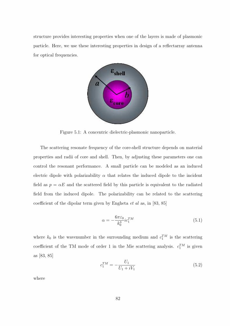
structure provides interesting properties when one of the layers is made of plasmonic
particle. Here, we use these interesting properties in design of a reflectarray antenna
for optical frequencies.
Figure 5.1: A concentric dielectric-plasmonic nanoparticle.
The scattering resonate frequency of the core-shell structure depends on material
properties and radii of core and shell. Then, by adjusting these parameters one can
control the resonant performance. A small particle can be modeled as an induced
electric dipole with polarizability α that relates the induced dipole to the incident
field as p = αE and the scattered field by this particle is equivalent to the radiated
field from the induced dipole. The polarizability can be related to the scattering
coefficient of the dipolar term given by Engheta et al as, in [83, 85]
α = −6πε0
k30
icTM1 (5.1)
where k0 is the wavenumber in the surrounding medium and cTM1 is the scattering
coefficient of the TM mode of order 1 in the Mie scattering analysis. cTM1 is given
as [83, 85]
cTM1 = − U1
U1 + iV1
(5.2)
where
82
U1 =
j1(k1b) j1(k2b) y1(k2b) 0
j1(k1b)/ε1 j1(k2b)/ε2 y1(k2b)/ε2 0
0 j1(k2a) y1(k2a) j1(k0a)
0 j1(k2a)/ε2 y1(k2a)/ε2 j1(k0a)/ε0
(5.3)
V1 =
j1(k1b) j1(k2b) y1(k2b) 0
j1(k1b)/ε1 j1(k2b)/ε2 y1(k2b)/ε2 0
0 j1(k2a) y1(k2a) y1(k0a)
0 j1(k2a)/ε2 y1(k2a)/ε2 y1(k0a)/ε0
(5.4)
Here, j1(x) and y1(x) are the first-order spherical Bessel functions of the first and
second kind. j1(x) stands for ∂(xj1(x))/∂x and y1(x) is similarly defined. ε1, ε2 are the
permittivity of the core and of the shell, respectively, while k1, k2 are the wavenumbers
in each respective region. The outer and inner radii of the particle are denoted as a
and b.
If one follows the closed form equation which has been obtained for cTM1 , it will
be seen that by adjusting the ratio b/a or the permittivities of core and shell, the
scattering resonance can be tailored at different wavelength range. In this study, a
Drude material is used to describe the frequency dependence of the permittivity of
silver which is the shell material, i.e.
ε(ω) = ε0
(1− ω2
p
ω(ω + iγp)
)(5.5)
where ωp is the bulk resonant frequency of the material, and damping factor γp repre-
sents the losses present. (In this study, ωp = 2π × 2000THz and γp = 0.001ωp)
Fig. 5.2 shows the magnitude and phase of the polarizability α of a concentric
nanoshell particle for different core materials and for different b/a ratios (see Fig. 5.1(a)
for the geometry of particle). Operating wavelength is 357.1 nm and εshell = (−4.67+
83

.01i)ε0. The outer radius is a = 22.5 nm and in Fig. 5.2(a), b/a is assumed to be 0.533.
Fig. 5.2(b) shows the performance vs b/a when εcore = 3ε0. As seen, due to the shift
in resonant frequency, the phase performance changes and these particles can be used
for a reflectarray antenna. In this study we use the same b/a for all the elements and
change the core permittivity to control the phase (as this will be easier for our FDTD
analysis).
0 1 2 3 4 5 6 70
1
2
3
4
5
6
7
88
εcore
|α| (1
0−
2ε 0
λ03)
0
0.2
0.4
0.6
0.8
11
Arg
(α
) (π
)
Magnitude Phase
(a)
0 0.2 0.4 0.6 0.8 10
1
2
3
4
5
6
7
8
b/a
|α| (1
0−
2ε 0
λ03)
0 0.2 0.4 0.6 0.8 10
0.2
0.4
0.6
0.8
1
Arg
(α
) (π
)
PhaseMagnitude
(b)
Figure 5.2: Magnitude and phase of the polarizability α of a concentric nanoshellparticle vs: (a) the permittivity of core when b/a = 0.533 and, (b) the ratio of radiib/a when εcore = 3ε0. Operating wavelength is 357.1 nm and the shell is made of silver[εshell = (−4.67 + .01i)ε0].
5.3 Optical Reflectarray Nanoantenna
To establish an optical reflectarray nanoantenna, one needs to design an array of nano-
radiators where each of them is tailored properly to provide a desired reflection phase,
where as a result the array can re-direct and scan the beam in a specific direction.
Having an array of nanoradiators allows narrowing the radiation beam. Thus, the
reflectarray nanoantenna can successfully scan a directive optical radiation beam. This
will be of significant interest for optical far-field engineering.
84
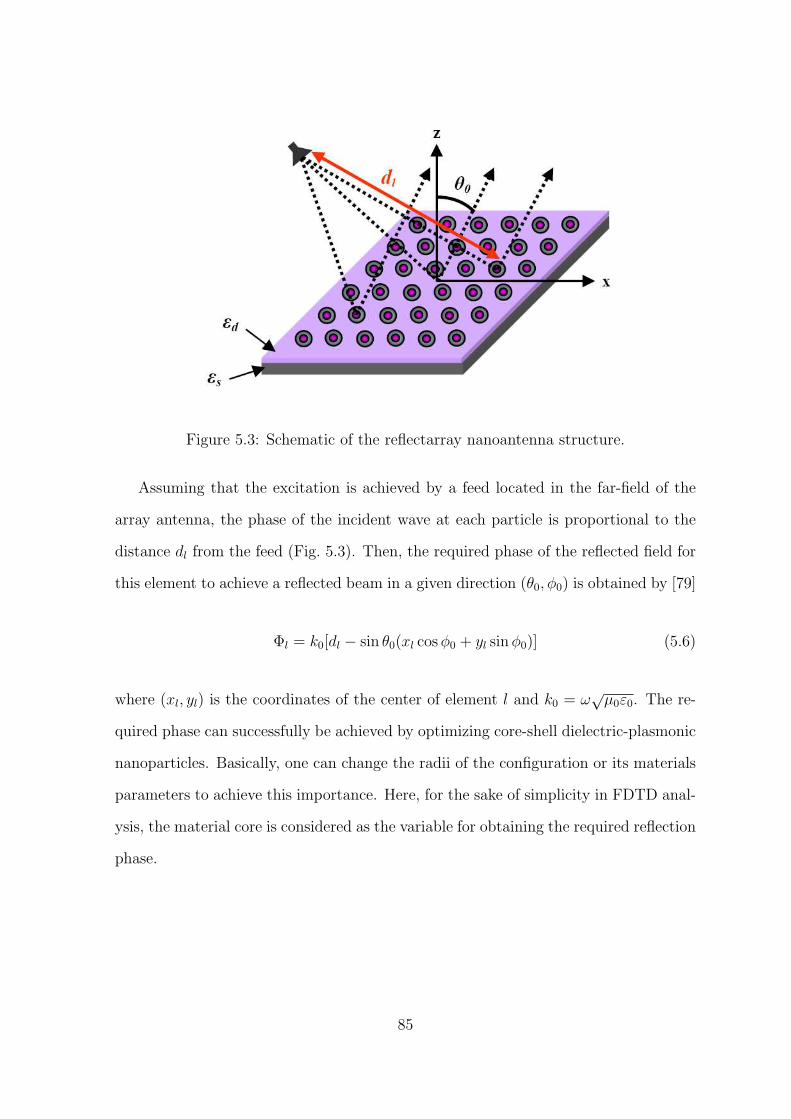
Figure 5.3: Schematic of the reflectarray nanoantenna structure.
Assuming that the excitation is achieved by a feed located in the far-field of the
array antenna, the phase of the incident wave at each particle is proportional to the
distance dl from the feed (Fig. 5.3). Then, the required phase of the reflected field for
this element to achieve a reflected beam in a given direction (θ0, φ0) is obtained by [79]
Φl = k0[dl − sin θ0(xl cos φ0 + yl sin φ0)] (5.6)
where (xl, yl) is the coordinates of the center of element l and k0 = ω√
µ0ε0. The re-
quired phase can successfully be achieved by optimizing core-shell dielectric-plasmonic
nanoparticles. Basically, one can change the radii of the configuration or its materials
parameters to achieve this importance. Here, for the sake of simplicity in FDTD anal-
ysis, the material core is considered as the variable for obtaining the required reflection
phase.
85

5.3.1 Reflection-Phase Synthesis
In order to characterize the radiating element of an array, the effect of the surrounding
elements needs to be taken into account. The exact method is to do measurement
by placing the element in complete array. For a large array of elements, this will
be costly and time consuming. The waveguide simulator approach provides a simple
and efficient way to determine the performance of the radiating elements in a large
array antenna [81, 86]. To achieve this, one can envision a nanoparticle inside the
array as a periodic configuration and then applied a full wave numerical analysis to
demonstrate the reflection phase from the array configuration. A finite difference time
domain (FDTD) [32–34] approach with periodic boundary condition (PBC) is applied
to characterize the performance of periodic array of nanoparticles.
Let us first highlight the scattering performance of a core-shell nanosphere. Fig. 5.4
illustrates the FDTD simulation of the particle having a = 22.5 nm, b/a = 0.533, silver
as the shell material and εcore = 3ε0. In the FDTD model, the computational domain
is configured with cubical Yee cells with ∆ = 0.75 nm and the core-shell structure is
illuminated by a plane wave having x-polarized electric field and traveling in the -z
direction. The sphere is placed at the center of computational domain (0, 0, 0) and the
scattered field is stored at (0, 0, 100∆) in front of the concentric sphere. The scattered
field is plotted in Fig. 5.4. The polarizability α of the same particle based on Mie
theory is also shown in Fig. 5.4. These two graphs can be compared in regard of the
position of resonances. A good comparison between the full wave numerical analysis
and theoretical model is established. At resonance point (λ0 = 357.1 nm) the error is
less than 4% which can be smaller by choosing a smaller Yee cell.
The array of nanoparticles is investigated next. The objective is to successfully
tailor the reflection phase from a nanoparticle located inside the array to the value
of interest. To accomplish this, the FDTD is applied to characterize one unit-cell of
the periodic structure (array of particles in free-space) and determine the phase of
86
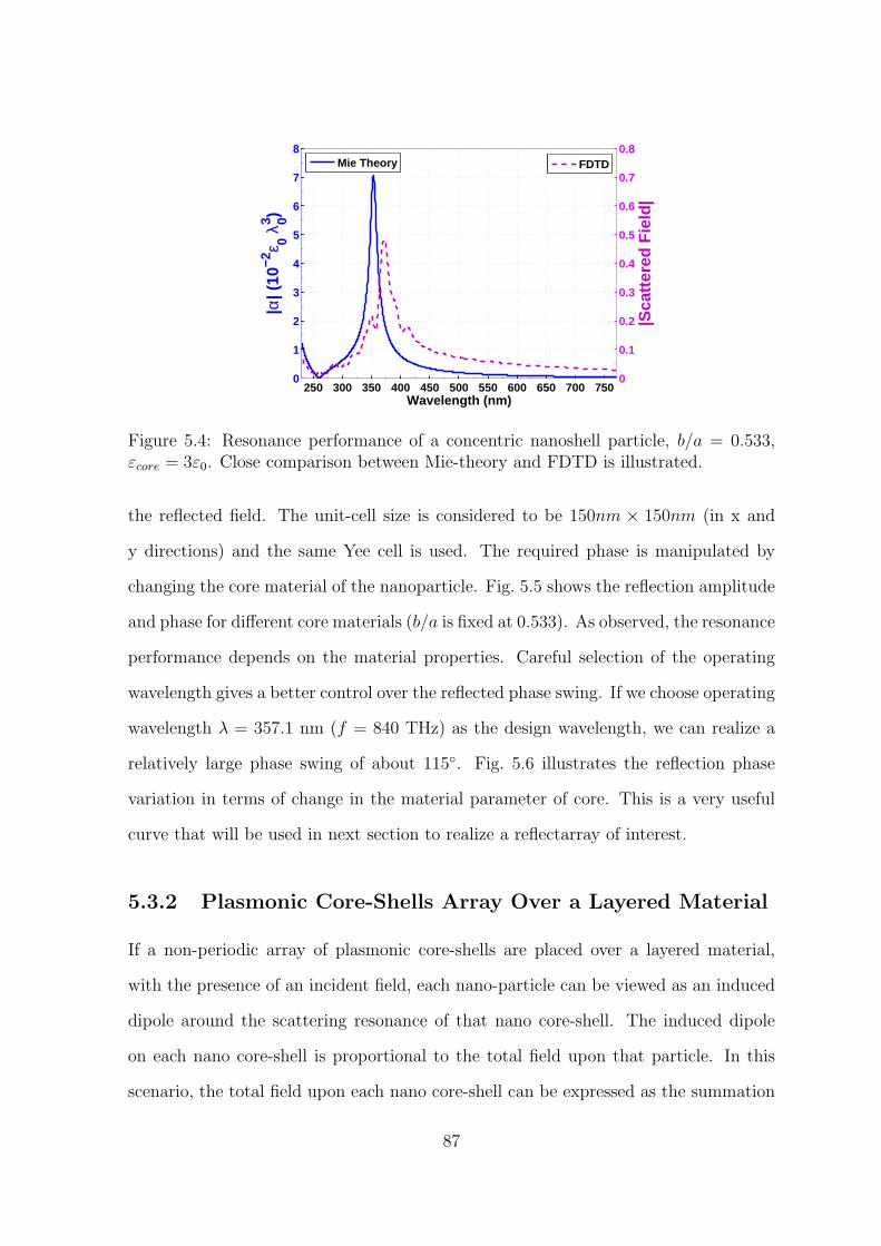
250 300 350 400 450 500 550 600 650 700 7500
1
2
3
4
5
6
7
8
Wavelength (nm)
|α| (
10−2
ε 0 λ03 )
0
0.1
0.2
0.3
0.4
0.5
0.6
0.7
0.8
|Sca
ttere
d F
ield
|
Mie Theory FDTD
Figure 5.4: Resonance performance of a concentric nanoshell particle, b/a = 0.533,εcore = 3ε0. Close comparison between Mie-theory and FDTD is illustrated.
the reflected field. The unit-cell size is considered to be 150nm × 150nm (in x and
y directions) and the same Yee cell is used. The required phase is manipulated by
changing the core material of the nanoparticle. Fig. 5.5 shows the reflection amplitude
and phase for different core materials (b/a is fixed at 0.533). As observed, the resonance
performance depends on the material properties. Careful selection of the operating
wavelength gives a better control over the reflected phase swing. If we choose operating
wavelength λ = 357.1 nm (f = 840 THz) as the design wavelength, we can realize a
relatively large phase swing of about 115. Fig. 5.6 illustrates the reflection phase
variation in terms of change in the material parameter of core. This is a very useful
curve that will be used in next section to realize a reflectarray of interest.
5.3.2 Plasmonic Core-Shells Array Over a Layered Material
If a non-periodic array of plasmonic core-shells are placed over a layered material,
with the presence of an incident field, each nano-particle can be viewed as an induced
dipole around the scattering resonance of that nano core-shell. The induced dipole
on each nano core-shell is proportional to the total field upon that particle. In this
scenario, the total field upon each nano core-shell can be expressed as the summation
87

300 325 350 375 400 425 450 475 5005000
0.1
0.2
0.3
0.4
0.5
0.6
Wavelength (nm)
Refl
ecti
on
Co
eff
icie
nt
εcore
= 1ε0
εcore
= 2ε0
εcore
= 3ε0
(a) (b)
Figure 5.5: FDTD simulated results for different core materials and construction ofphase design curve: (a) reflection amplitude and, (b) reflection phase
1 1.5 2 2.5 3 3.5 4−120
−100
−80
−60
−40
−20
0
20
εcore
Ref
lect
ion
Pha
se (
deg)
Figure 5.6: Phase of reflection coefficient vs. the core permittivity at λ0 = 357.1 nm
88
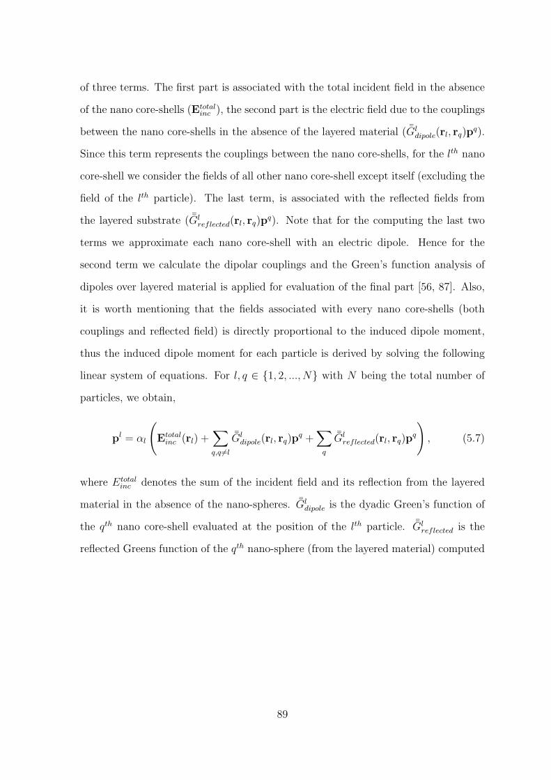
of three terms. The first part is associated with the total incident field in the absence
of the nano core-shells (Etotalinc ), the second part is the electric field due to the couplings
between the nano core-shells in the absence of the layered material ( ¯Gldipole(rl, rq)p
q).
Since this term represents the couplings between the nano core-shells, for the lth nano
core-shell we consider the fields of all other nano core-shell except itself (excluding the
field of the lth particle). The last term, is associated with the reflected fields from
the layered substrate ( ¯Glreflected(rl, rq)p
q). Note that for the computing the last two
terms we approximate each nano core-shell with an electric dipole. Hence for the
second term we calculate the dipolar couplings and the Green’s function analysis of
dipoles over layered material is applied for evaluation of the final part [56, 87]. Also,
it is worth mentioning that the fields associated with every nano core-shells (both
couplings and reflected field) is directly proportional to the induced dipole moment,
thus the induced dipole moment for each particle is derived by solving the following
linear system of equations. For l, q ∈ 1, 2, ..., N with N being the total number of
particles, we obtain,
pl = αl
(Etotal
inc (rl) +∑
q,q 6=l
¯Gldipole(rl, rq)p
q +∑
q
¯Glreflected(rl, rq)p
q
), (5.7)
where Etotalinc denotes the sum of the incident field and its reflection from the layered
material in the absence of the nano-spheres. ¯Gldipole is the dyadic Green’s function of
the qth nano core-shell evaluated at the position of the lth particle. ¯Glreflected is the
reflected Greens function of the qth nano-sphere (from the layered material) computed
89
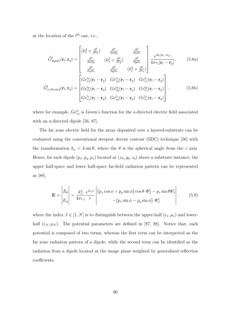
at the location of the lth one, i.e.,
¯Gldipole(rl, rq) =
(k21 + ∂2
∂2x) ∂2
∂x∂y∂2
∂x∂z
∂2
∂x∂y(k2
1 + ∂2
∂2y) ∂2
∂y∂z
∂2
∂x∂z∂2
∂y∂z(k2
1 + ∂2
∂2z)
eik1|rl−rq |
4πε1|rl − rq| , (5.8a)
¯Glreflected(rl, rq) =
Gelxrx(rl − rq) Gelx
ry(rl − rq) Gelxrz(rl − rq)
Gelyrx(rl − rq) Gely
ry(rl − rq) Gelyrz(rl − rq)
Gelzrx(rl − rq) Gelz
ry(rl − rq) Gelzrz(rl − rq)
. (5.8b)
where for example, Gelzrx is Green’s function for the z-directed electric field associated
with an x-directed dipole [56, 87].
The far zone electric field for the array deposited over a layered-substrate can be
evaluated using the conventional steepest decent contour (SDC) technique [56] with
the transformation kρ = k sin θ, where the θ is the spherical angle from the z axis.
Hence, for each dipole (px, py, pz) located at (x0, y0, z0) above a substrate instance, the
upper half-space and lower half-space far-field radiation pattern can be represented
as [88],
E =
∣∣∣∣∣∣∣Eθ
Eφ
∣∣∣∣∣∣∣=
k2J
4πεJ
eikJr
r
∣∣∣∣∣∣∣
(px cos φ + py sin φ
)cos θ Φ2
J − pz sin θΦ1J
−(px sin φ− py sin φ
)Φ3
J
∣∣∣∣∣∣∣. (5.9)
where the index J ∈ [1, N ] is to distinguish between the upper-half (ε1, µ1) and lower-
half (εN , µN). The potential parameters are defined in [87, 88]. Notice that, each
potential is composed of two terms, whereas the first term can be interpreted as the
far zone radiation pattern of a dipole, while the second term can be identified as the
radiation from a dipole located at the image plane weighted by generalized reflection
coefficients.
90

5.4 Array Design and Scanned-Beam Characteris-
tics
In this study, two reflectarray designs (including 6 × 6 elements) for beam scanning
at 15 and 30 are considered. The geometry of reflectarray is depicted in Fig. 5.3.
The center of array is placed at (0, 0, 0). For the first design the feed is located at
(xf = yf = zf ) = (−0.4µm, 0, 2.25µm), and for the second design it is at (xf =
yf = zf ) = (−0.4µm, 0, 4.5µm). The feed excitation is modeled with an infinitesimal
electric dipole which is polarized along the x-direction and operates at λ0 = 357.1nm.
In order to ensure field radiation only in one side of the antenna, the array antenna
is deposited on a silver layer coated by a dielectric material. The silver layer has a
thickness of 35.7nm = 0.1λ0 and the same material as the shell (εrs = −4.67 + 0.01i).
The dielectric material is made of a thin SiO2 film with εrd = 2.2 and thickness of
3.571nm. Considering the thin thicknesses of the substrate layers, they do not have
much effects on the reflection phase, and they will only help to suppress the back
radiation. Hence, one can still use the reflection phase curve demonstrated in Fig. 5.6
for an array of core-shell nanoparticles located in free-space. This will be validated
later by both our theoretical and full-wave numerical models.
Let us first consider the 15 scan angle case (θ0 = 15, φ0 = 0). From Eq. (5.6), one
can first determine the required reflection phases for the array elements. Then, from
Fig. 5.6 the required material parameters for the nanoparticles cores are evaluated, as
given in Table 5.1(a). The cores materials range from εrd = 1.2 to εrd = 3.9. The Mie
theory formulations discussed in section 5.3 is used to determine the equivalent dipole
modes for each of the nanoshells as illustrated in Table 5.2(a). Since the values of pys
are much smaller than those of px and pz dipoles, they are not shown in this table.
The values are normalized to maximum of |p|. The radiation pattern for the array
of dipoles elements located above the layered substrate is obtained in Fig. 5.7(a).
91

Table 5.1: Core relative permittivity of nanoantenna array elements: (a) θ0 = 15, and(b) θ0 = 30.
(a) θ = 15 (b) θ = 30
m=1 m=2 m=3 m=4 m=5 m=6 m=1 m=2 m=3 m=4 m=5 m=6n=1 1.2 2.25 2.7 2.8 2.84 2.8 1.2 2.1 2.7 2.88 3.47 3.91n=2 1.8 2.67 2.87 3.11 3.3 3.04 1.6 2.53 2.77 3.04 3.76 4.62n=3 2.09 2.76 3.0 2.59 3.69 3.51 1.7 2.59 2.81 2.27 3.92 4.77n=4 2.09 2.76 3.0 2.59 3.69 3.51 1.7 2.59 2.81 2.27 3.92 4.77n=5 1.8 2.67 2.87 3.11 3.3 3.04 1.6 2.53 2.77 3.04 3.76 4.62n=6 1.2 2.25 2.7 2.8 2.84 2.8 1.2 2.1 2.7 2.88 3.47 3.91
This validates a successful 15 beam scanning for the reflected field (25 difference
compared to the beam illumination). The half-power beamwidth is 22 which is an
improvement of about 4 times compared to dipole excitation itself (which has a 90
beamwidth). Note that, the obtained beamwidth for reflectarray is in good comparison
with the performance of a uniform array offering 19 beamwidth [23]. Thus, the 6× 6
reflectarray nanoparticles antenna successfully scans a narrow beam optical emission.
One can reduce the beamwidth even much more by simply increasing the number of
array elements [23]. The magnitude (dB) and phase of the x-directed electric field in
an x-y plane located at z = 0.5λ0 above the plane of nano core-shells are also depicted
in Figs. 5.8.
−12
−9
−6
−3
0
60
120
30
150
0
180
30
150
60
120
90 90
(a)
−12
−9
−6
−3
0
60
120
30
150
0
180
30
150
60
120
90 90
(b)
Figure 5.7: Radiation pattern in the x-z plane at λ0 = 357.1 nm: (a) θ0 = 15, and(b) θ0 = 30.
92

Table 5.2: Induced dipoles, pxs and pzs: (a) θ0 = 15, and (b) θ0 = 30.(a) θ = 15
m=1 m=2 m=3 m=4 m=5 m=6
n=10.57e−i0.99π 0.84e−i0.67π 0.63e−i0.41π 0.68e−i0.31π 0.67e−i0.01π 0.56ei0.18π
0.30e−i0.3π 0.25ei0.06π 0.27ei0.45π 0.20ei0.8π 0.20e−i0.88π 0.07e−i0.65π
n=20.79e−i0.97π 0.66e−i0.74π 0.55e−i0.57π 0.56e−i0.48π 0.5e−i0.07π 0.5ei0.07π
0.39e−i0.19π 0.40ei0.14π 0.39ei0.45π 0.30ei0.87π 0.27e−i0.87π 0.08e−i0.59π
n=30.76e−i0.95π 0.61e−i0.78π 0.56e−i0.63π 0.94e−i0.61π 0.33ei0.01π 0.28ei0.15π
0.26e−i0.04π 0.39ei0.29π 0.32ei0.5π 0.33ei0.97π 0.18e−i0.92π 0.03ei0.16π
n=40.76e−i0.95π 0.61e−i0.78π 0.56e−i0.63π 0.94e−i0.61π 0.33ei0.01π 0.28ei0.15π
0.26e−i0.04π 0.39ei0.29π 0.32ei0.5π 0.33ei0.97π 0.18e−i0.92π 0.03ei0.16π
n=50.79e−i0.97π 0.66e−i0.74π 0.55e−i0.57π 0.56e−i0.48π 0.5e−i0.07π 0.5ei0.07π
0.39e−i0.19π 0.40ei0.14π 0.39ei0.45π 0.30ei0.87π 0.27e−i0.87π 0.08e−i0.59π
n=60.57e−i0.99π 0.84e−i0.67π 0.63e−i0.41π 0.68e−i0.31π 0.67e−i0.01π 0.56ei0.18π
0.30e−i0.3π 0.25ei0.06π 0.27ei0.45π 0.20ei0.8π 0.20e−i0.88π 0.07e−i0.65π
(b) θ = 30
m=1 m=2 m=3 m=4 m=5 m=6
n=10.74ei0.86π 0.82e−i0.61π 0.74e−i0.16π 0.41ei0.17π 0.55ei0.55π 0.24e−i0.93π
0.58e−i0.4π 0.39e−i0.05π 0.33ei0.62π 0.25e−i0.89π 0.12e−i0.38π 0.04ei0.46π
n=20.77ei0.9π 0.37e−i0.55π 0.68e−i0.24π 0.30e−i0.01π 0.48ei0.55π 0.12e−i0.95π
0.88e−i0.34π 0.57e−i0.02π 0.41ei0.57π 0.33e−i0.94π 0.14e−i0.42π 0.02ei0.46π
n=30.78ei0.9π 0.51e−i0.5π 0.54e−i0.26π 0.31e−i0.04π 0.53ei0.55π 0.10e−i0.85π
0.71e−i0.34π 0.58ei0.02π 0.42ei0.54π 0.26e−i0.8π 0.12e−i0.19π 0.07ei0.84π
n=40.78ei0.9π 0.51e−i0.5π 0.54e−i0.26π 0.31e−i0.04π 0.53ei0.55π 0.10e−i0.85π
0.71e−i0.34π 0.58ei0.02π 0.42ei0.54π 0.26e−i0.8π 0.12e−i0.19π 0.07ei0.84π
n=50.77ei0.9π 0.37e−i0.55π 0.68e−i0.24π 0.30e−i0.01π 0.48ei0.55π 0.12e−i0.95π
0.88e−i0.34π 0.57e−i0.02π 0.41ei0.57π 0.33e−i0.94π 0.14e−i0.42π 0.02ei0.46π
n=60.74ei0.86π 0.82e−i0.61π 0.74e−i0.16π 0.41ei0.17π 0.55ei0.55π 0.24e−i0.93π
0.58e−i0.4π 0.39e−i0.05π 0.33ei0.62π 0.25e−i0.89π 0.12e−i0.38π 0.04ei0.46π
Figure 5.8: Near-field (Ex) of the reflectarray for 15 beam scanning [Fig. 5.7(a)] in aplane located at 0.5λ0 above the nanoantenna: (a) magnitude (dB), and (b) phase.
93
The similar procedure can be followed to design a 6 × 6 array for 30 scan angle.
Table 5.1(b) illustrates the required core material parameters where they range from
εrd = 1.2 to εrd = 4.8. Induced dipole modes for the nanoparticles are summarized in
Table 5.2(b). Fig. 5.7(b) illustrates the radiation characteristic. The radiation pattern
shows that the main beam is directed along θ0 = 30 whose half-power beamwidth is
about 30. Figs. 5.9 show the distribution of the Ex in an x-y plane, 0.5λ0 above the
nano particles’ plane.
A full-wave FDTD numerical analysis is also applied to validate our dipole-modes
modeling results, and further explore the effects of finite-size substrate on the radiation
characteristics. To accurately model thin silver shells in FDTD, we need to use very
small-size Yee cells, hence characterizing the whole 6 × 6 array would be very huge
and time-consuming. Instead, we model the core-shell structures with their equivalent
induced dipoles (using Mie analytical model), and then we integrate them with FDTD
numerical technique. This is called hybrid FDTD-dipolar mode technique. In the
FDTD simulation, each nanoparticle is modeled by its induced dipoles given in Table
5.2. There will be 6 × 6 sets of dipoles on top of the finite-size layered substrate.
Since the py is about ten times smaller than px and pz, in our simulation we ignored
the pys. At operating wavelength, λ0 = 357.1nm, the slab size in transverse plane is
3λ0× 3λ0. The hybrid FDTD-dipolar modes is applied and the radiation patterns are
demonstrated in Fig. 5.10. Very good comparisons in compared to the full theoretical
model are presented. The side lobes are slightly increased due to the wave diffractions
from the substrate edges. The FDTD results validate successfully the concept and
radiation performance of the optical reflectarray nanoantennas investigated in this
study.
Frequency sensitivity of the reflectarray design is also explored in this study. The
radiation patterns for scanning 30 at different frequencies f = 0.9f0, 0.95f0, 1.05f0, 1.1f0
are plotted in Fig. 5.11. By changing the frequency, both the size and material (for the
silver coatings) parameters of the nanoparticles will be changed affecting the radiation
94
pattern and degrading the performance.
Figure 5.9: Near-field (Ex) of the reflectarray for 30 beam scanning [Fig. 5.7(b)] in aplane located at 0.5λ0 above the nanoantenna: (a) magnitude (dB), and (b) phase.
−12
−9
−6
−3
0
60
120
30
150
0
180
30
150
60
120
90 90
(a)
−12
−9
−6
−3
0
60
120
30
150
0
180
30
150
60
120
90 90
(b)
Figure 5.10: FDTD radiation pattern in the x-z plane at λ0 = 357.1 nm: (a) θ0 = 15,and (b) θ0 = 30. Good comparisons compared to dipole-modes theoretical results(5.7) are observed.
5.5 Conclusions
This study presented the concept of reflectarray nanoantenna implementation in op-
tics for the first time, with the use of array of core-shell nanoparticles. Optimized
95
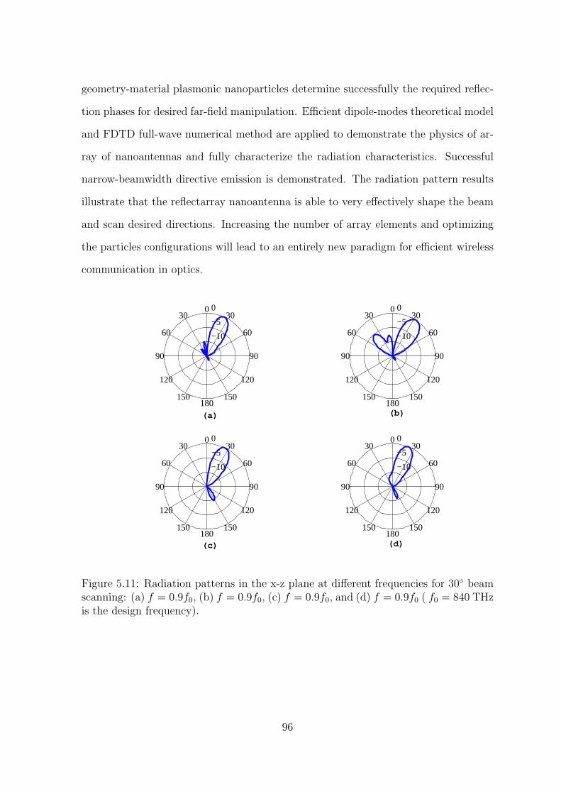
geometry-material plasmonic nanoparticles determine successfully the required reflec-
tion phases for desired far-field manipulation. Efficient dipole-modes theoretical model
and FDTD full-wave numerical method are applied to demonstrate the physics of ar-
ray of nanoantennas and fully characterize the radiation characteristics. Successful
narrow-beamwidth directive emission is demonstrated. The radiation pattern results
illustrate that the reflectarray nanoantenna is able to very effectively shape the beam
and scan desired directions. Increasing the number of array elements and optimizing
the particles configurations will lead to an entirely new paradigm for efficient wireless
communication in optics.
−10
−5
0
60
120
30
150
0
180
30
150
60
120
90 90
−10
−5
0
60
120
30
150
0
180
30
150
60
120
90 90
−10
−5
0
60
120
30
150
0
180
30
150
60
120
90 90
−10
−5
0
60
120
30
150
0
180
30
150
60
120
90 90
(b)(a)
(c) (d)
Figure 5.11: Radiation patterns in the x-z plane at different frequencies for 30 beamscanning: (a) f = 0.9f0, (b) f = 0.9f0, (c) f = 0.9f0, and (d) f = 0.9f0 ( f0 = 840 THzis the design frequency).
96

Chapter 6
Optical Nanoloops Array Antenna
6.1 Introduction
Antenna is a key element in the microwave spectrum to enable wireless data commu-
nication. The extension of this concept into the optics has many applications and has
been a growing research in recent years [87, 89–96]. Among the technological appli-
cations for optical antennas one can find high-resolution microscopy and spectroscopy,
optical sensors, lasing, solar cells and efficient solid-state light sources, and it has also
become important in biotechnology and medicine.
As we discussed in previous chapters, noble metals in optics offer negative per-
mittivity parameter where a high scattering performance in subwavelength sizes can
be achieved. Arraying subwavelength plasmonic elements in unique configurations
can successfully engineer the optical emission. Recently, optical nanodipoles made of
plasmonic materials and their arrangements in Yagi-Uda definition have been theoret-
ically and experimentally characterized to modify optical emission by various groups
[87, 89–92, 94, 97]. The common Yagi-Uda antenna achieves a high directivity by
placing several scatterers around a resonant feed element. On one side of the feed, the
scatterers are slightly capacitive called directors, and the elements on the other side
are inductive and called reflectors. To use this concept in optics, it has been suggested
97
to place an emitter in an array of properly tuned particles. In recent works, plasmonic
dipoles and core-shell nanospheres have been introduced as the elements of a Yagi-Uda
antenna. In order to achieve a higher directivity, we propose in this chapter to use
loop elements in Yagi-Uda array. Resonant loop antennas are attractive because of
their symmetric radiation patterns and the potential for offering higher directivity. In
this chapter, we first review the optical nanodipole antenna and study the radiation
characteristic of a Yagi-Uda antenna with plasmonic dipoles as the radiating elements.
Then, we investigate the plasmonic nanoloop element and design a highly directed
array antenna for optical frequencies.
6.2 Optical Nanodipole Antennas
Dipole antennas are some of the oldest, simplest and cheapest for many applications
in microwave. In traditional antenna design, characteristic lengths L of antennas are
directly related to the wavelength λ of the incoming (or outgoing) radiation. For ex-
ample, an ideal half-wave dipole antenna is made of a thin rod of length L = λ/2.
However, at optical frequencies an antenna no longer depends to the external wave-
length but to a shorter effective wavelength λeff which depends on the material prop-
erties and the shape of structure [91, 96]. In chapter 4, we studied the effects of
the shape and material dispersion of epsilon negative (ENG) radiators on their reso-
nance characteristics. We demonstrated that the material polarization can successfully
provide resonance radiation at the negative material constitutive parameters. Here,
we consider a small plasmonic particle to study its radiation characteristics and its
performance in an array arrangement.
Let us consider a dipole antenna made of a cubic rod of dielectric material ε(ω),
length H = 120 nm and width W = 30 nm (H/W = 4). Fig. 6.1(a) shows the
geometry of our model. The frequency dependent dielectric function of the metal is
98

described by the Drude model as below,
ε(ω) = ε0
(1− ω2
p
ω(ω + iγp)
), (6.1)
where ωp is the plasma frequency of the material, and damping factor γp represents
the losses present. Here, the dipole antenna is made of Silver (ωp = 2π×2175THz and
γp = 2π × 4.35THz [98]).
An incident plane wave with wavelength λ having z-polarized electric field and
traveling in the x direction illuminates the structure and polarizes the material. The
material polarization provides resonance radiation at a negative material constitutive
parameter. Finite Difference Time Domain technique [34] is applied to simulate the
structure and determine field characteristics. In FDTD model, the computational do-
main is configured with cubical Yee cells with ∆ = 5nm and the structure is illuminated
by a plane wave. The dipole is placed at the center of computational domain (0,0,0)
and the scattered field is stored at (0,0,50∆) in front of the dipole. The scattered
field is plotted in Fig. 6.1(b). A high scattering performance at resonant wavelength
of λ = 760 nm is observed. At resonance, the plasmonic dipole has subwavelength size
of total length of H = λ/6.3.
To study the radiation performance of the resonant dipole, we excite the dipole by
an Ez source placed at the center of dipole (0, 0, 0). To study the angular dependence
of the emission, the angular directivity D(θ, φ) is calculated. The directivity D at a
giving direction (θ, φ) is defined as [23],
D(θ, φ) = 4πU(θ, φ)
Prad
(6.2)
where Prad is the total radiated power of the whole antenna system, U(θ, φ) is the
radiation intensity at the observation angel (θ, φ). The directivity D(θ) in the plane
φ = 0 is plotted in Fig. 6.2. The maximum directivity of D = 1.9dB is obtained.
99

(a)
0.4 0.6 0.8 1 1.20
0.05
0.1
0.15
0.2
0.25
Wavelength (µm)M
agn
itu
de
of
Ez
(b)
Figure 6.1: A single plasmonic dipole antenna illuminated by an z-polarized electricfield plane wave, W = 30nm, H = 120nm: (a) structure, (b) resonance performance.
−3
−1
1
3
5
60
120
30
150
0
180
30
150
60
120
90 90
Figure 6.2: Directivity (in dB) for resonant plasmonic dipole antenna in plane φ = 0.Maximum directivity is 1.9dB.
6.2.1 Optical Nanodipole Yagi-Uda Antennas
In the previous section, we discussed that plasmonic particles at scattering resonance
can be used as optical antenna elements. Arranging the antenna elements in an array
design will enhance radiation characteristics. Yagi-Uda antenna concept is an approach
of designing an endfire-type optical antenna array.
Yagi-Uda antenna is one of the most popular endfire antenna designs in the RF/
microwave domain. It was first developed and described by S. Uda in Japan [99] and
100

later on discussed and made famous by H. Yagi [100]. The Yagi-Uda antenna array
consists of several linear dipole antennas in which only one of them is driven by the
source. The other elements are parasitic radiating elements whose current are induced
by the mutual coupling to the source antenna and to each other. To design a Yagi-Uda
antenna, the impedance of each element on the right hand side of the driving element
should be capacitive and its current leads the inducing emf. The element on the left
hand side is the opposite. The key feature in this design is the length of each element.
The parasitic elements are not of the same length. The elements on the right hand
side of the driving element are a little bit shorter than the resonant length, while the
one on the left is a little longer.
The idea of Yagi-Uda antenna array have been transplanted into optical nanoan-
tenna array design by different authors [82, 97]. To apply the design concept of the
Yagi-Uda array, we begin the design process with three elements: One reflector, one
emitter, and one director. Fig. 6.3 shows the structure. The length of emitter based
on the pervious section is set to be he = 120nm to have the strong resonance at
λ = 760nm but the length of reflector and director have been modified. We declare
the particle at the left side an “inductive” element because the effective induced cur-
rent of the dipole has a phase that lags with respect to the phase of the incident field.
For a similar reason, the particle at the right is a “capacitive” one. The directivity
D(θ) in the plane φ = 0 is plotted in Fig. 6.4. The maximum directivity of D = 3.6dB
is obtained.
In RF/microwave domain, it is discovered that arrays with more than one director
can provide radiation patterns with narrower bandwidth. Fig. 6.5 shows an array of
5 elements and the directivity D(θ) in the plane φ = 0 is plotted in Fig. 6.6. As seen,
the directivity is improved.
101

Figure 6.3: 3-element nano-optical Yagi-Uda antenna for an operating wavelength of760 nm. hr = 130nm, he = 120nm, hd = 105nm, d = 100nm.
−3
−1
1
3
5
60
120
30
150
0
180
30
150
60
120
90 90
Figure 6.4: Directivity (in dB) for the Nano-optical Yagi-Uda antenna shown inFig. 6.3in plane φ = 0. Maximum directivity is 3.6dB.
Figure 6.5: 5-element nano-optical Yagi-Uda antenna for an operating wavelength of760 nm. hr = 130nm, he = 120nm, hd = 105nm, d = 100nm.
102

−3
−1
1
3
5
60
120
30
150
0
180
30
150
60
120
90 90
Figure 6.6: Directivity (in dB) for the Nano-optical Yagi-Uda antenna shown in Fig. 6.5in plane φ = 0. Maximum directivity is 4.5dB.
6.3 Optical Nanoloop Antennas
A microwave metallic loop antenna goes to resonance where βb = 1, 2, 3, ...(b: mean
radius of a circular loop) [101]. This means the required minimum loop diameter to
achieve a high scattering is around 0.3λ. A different scenario is expected in optics
as the incident wave penetrates into the metal and gives rise to oscillation of the
free-electron gas generating surface plasmon (SP) modes [91]. The optical antenna
is scaled down by the effective wavelength of the plasmonic material which depends
on the material property and the shape of the structure [91, 96]. For instance, for a
rectangular loop antenna (constructed from four cubical arms), the higher the aspect
ratio of the metallic arms the higher the operating wavelength and thus the smaller
the size of the resonator.
Here, the physics of the plasmonic loop is integrated into the design of optical
nanoloops array antenna. First, we consider a single plasmonic loop antenna (rectan-
gular) of dielectric material ε(ω), side length l, and thickness t. Fig. 6.7 shows the
parameters used in our model. The frequency dependent dielectric function of the
metal is described by the Drude model Eq. (6.1). Here, the loop antenna is made of
Silver with ωp = 2π × 2175THz and γp = 2π × 4.35THz [98].
103

Figure 6.7: A single plasmonic loop antenna illuminated by an x-polarized electricfield plane wave, l = 85nm, t = 15nm.
An incident plane wave with wavelength λ illuminates the structure and polarizes
the material. The material polarization provides resonance radiation at a negative
material constitutive parameter.
Finite Difference Time Domain technique [34] is applied to simulate the structure
and determine field characteristics. In FDTD model, the computational domain is
configured with cubical Yee cells with ∆ = 5nm and the structure is illuminated by
a plane wave having x-polarized electric field and traveling in the −z direction. The
loop is placed at the center of computational domain (0,0,0) and the scattered field
is stored at (0,0,30∆) in front of the loop. The scattered field is plotted in Fig. 6.8.
A high scattering performance at resonant wavelength of λ = 1.34µm is observed. At
resonance, the plasmonic loop has subwavelength size of total length of 4l = λ/3.9.
The x- and y-components of polarized current distribution are plotted at the resonance
frequency in Figs. 6.9. A successful current circulation is observed.
To study the radiation performance of the resonant loop, we excite the loop by an
Ex source placed at (0, l/2, 0). The 3D power pattern is presented in Fig. 6.10. The
drawing is a series of patterns on planes of constant angles φ. Eφ is almost zero in
the vertical plane φ = 0, π, while Eθ is small in the vertical plane φ = π/2, 3π/2. The
D(θ) in two major planes, φ = 0 and π/2, are plotted in Figs. 6.11. The maximum
104
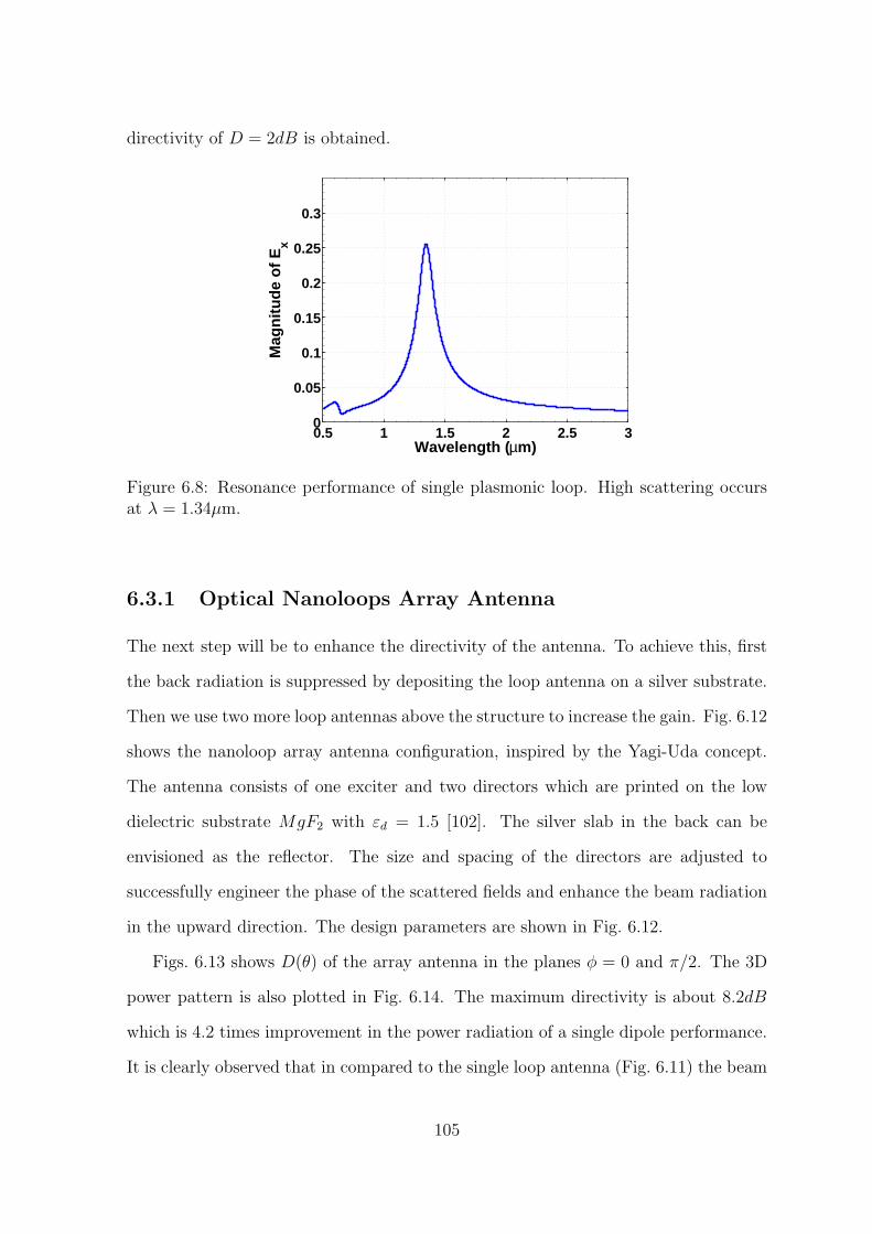
directivity of D = 2dB is obtained.
0.5 1 1.5 2 2.5 30
0.05
0.1
0.15
0.2
0.25
0.3
Wavelength (µm)
Mag
nit
ud
e o
f E
x
Figure 6.8: Resonance performance of single plasmonic loop. High scattering occursat λ = 1.34µm.
6.3.1 Optical Nanoloops Array Antenna
The next step will be to enhance the directivity of the antenna. To achieve this, first
the back radiation is suppressed by depositing the loop antenna on a silver substrate.
Then we use two more loop antennas above the structure to increase the gain. Fig. 6.12
shows the nanoloop array antenna configuration, inspired by the Yagi-Uda concept.
The antenna consists of one exciter and two directors which are printed on the low
dielectric substrate MgF2 with εd = 1.5 [102]. The silver slab in the back can be
envisioned as the reflector. The size and spacing of the directors are adjusted to
successfully engineer the phase of the scattered fields and enhance the beam radiation
in the upward direction. The design parameters are shown in Fig. 6.12.
Figs. 6.13 shows D(θ) of the array antenna in the planes φ = 0 and π/2. The 3D
power pattern is also plotted in Fig. 6.14. The maximum directivity is about 8.2dB
which is 4.2 times improvement in the power radiation of a single dipole performance.
It is clearly observed that in compared to the single loop antenna (Fig. 6.11) the beam
105

Figure 6.9: Polarized current on plasmonic loop at resonant wavelength λ = 1.34µm:(a) normalized |Jx| (dB), and (b) normalized |Jy| (dB). The current distribution issimilar to what one observes in microwave for a rectangular loop antenna with 4l ' λ(The size becomes subwavelength in optics.)
Figure 6.10: Far-zone power pattern for single plasmonic loop at the operating wave-length.
106

Figure 6.11: Directivity (in dB) for resonant plasmonic loop antenna in planes (a)φ = 0, and (b) φ = π/2 Maximum directivity is 2dB.
Figure 6.12: Schematic view of nanoloops antenna array. At operating wavelength ofλ = 1.34µm, the emitter element has the resonant size of 4l1 = 340nm=λ/3.9, andthe directors lengths are 4l2 = 4l3 = 260nm. The reflector spacing is t1 = 125nm,and the directors spacings are t2 = t3 = 375nm. The emitter and the directors areprinted on low dielectric substrates with εd = 1.5. The silver slab has the thickness ofts = 205nm. A finite-size structure of ls = 500nm in the transverse plane is considered.The yellow arrow shows the excitation.
107
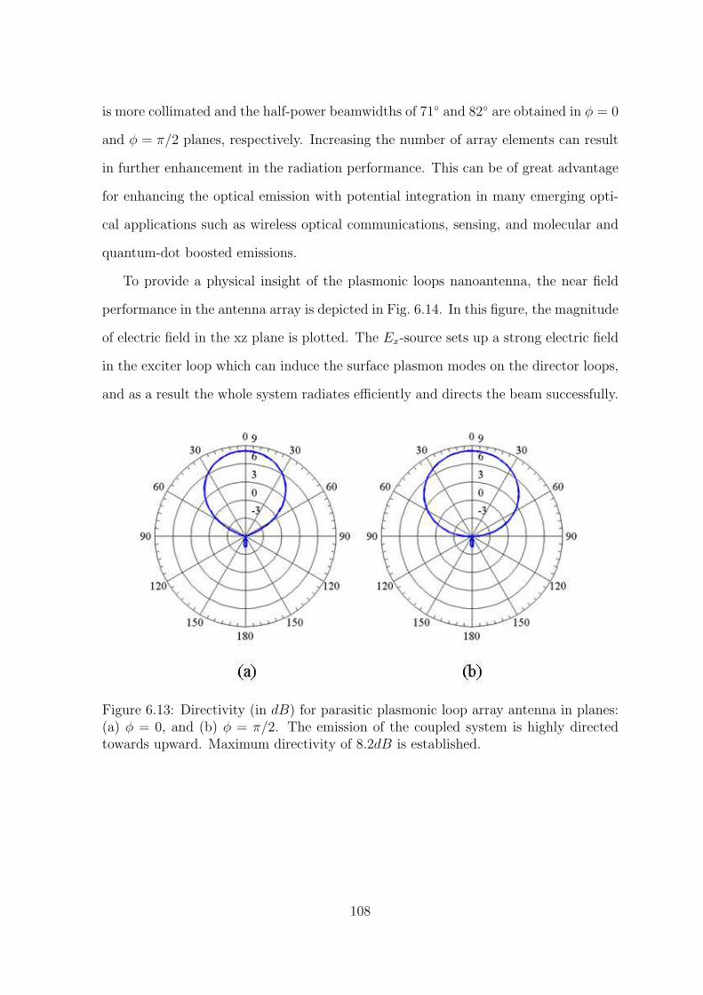
is more collimated and the half-power beamwidths of 71 and 82 are obtained in φ = 0
and φ = π/2 planes, respectively. Increasing the number of array elements can result
in further enhancement in the radiation performance. This can be of great advantage
for enhancing the optical emission with potential integration in many emerging opti-
cal applications such as wireless optical communications, sensing, and molecular and
quantum-dot boosted emissions.
To provide a physical insight of the plasmonic loops nanoantenna, the near field
performance in the antenna array is depicted in Fig. 6.14. In this figure, the magnitude
of electric field in the xz plane is plotted. The Ex-source sets up a strong electric field
in the exciter loop which can induce the surface plasmon modes on the director loops,
and as a result the whole system radiates efficiently and directs the beam successfully.
Figure 6.13: Directivity (in dB) for parasitic plasmonic loop array antenna in planes:(a) φ = 0, and (b) φ = π/2. The emission of the coupled system is highly directedtowards upward. Maximum directivity of 8.2dB is established.
108

Figure 6.14: Far-zone power pattern for the array antenna. The power is highlydirected towards the upper hemisphere and the back radiation is suppressed. Successfulcollimation in compared to Fig. 6.10 is illustrated.
x (µm)
z (µ
m)
−0.3 −0.2 −0.1 0 0.1 0.2 0.3
1.8
1.6
1.4
1.2
1.0
0.8
0.6
0.4
0.2
0.0−50
−40
−30
−20
−10
0
Figure 6.15: Electric field distribution induced on the nanoloops antenna array at theoperating wavelength of λ = 1.34µm (Normalized and plotted in dB.)
109

6.4 Conclusions
In summary, we have investigated a highly directive nanoantenna array whose ele-
ments are plasmonic nanoloops. The beam is collimated and high directivity of 8.2dB
is achieved by arraying three loops over a silver substrate where the total size in the z
direction does not exceed 1.125µm ' 0.8λ. The size in transverse direction is 500nm.
The resonant size of the plasmonic loop is scaled down by a factor of about 3.9 in
compared to the size of a microwave loop antenna. The directivity can even be more
enhanced by increasing the number of directors. The loop nanoantenna has the ad-
vantage of offering higher directivity in compared to the traditional dipole antenna
design. The nanoloops array concept proposed in this letter can provide significant
benefits for optical boosted emissions and relevant nanoscale applications.
110

Chapter 7
Conclusions and Recommendations
for Future Work
7.1 Summary and Contributions
This thesis reviewed the concept of Metamaterials and investigated some novel appli-
cations in near-field imaging and antenna design. The following subsections outline
the contributions of this dissertation.
7.1.1 Design and Development of All-Dielectric Metamateri-
als
In this dissertation, a comprehensive investigation of all-dielectric metamaterials is
addressed. The concept of electric and magnetic dipole modes generation for meta-
material development is presented. To achieve a metamaterial with desired figure of
merit, one needs to first create appropriate electric and magnetic dipole moments and
then tailor them to the application of interest. Primarily, the electric and magnetic
dipole moments are the basic foundations for making metamaterials. We implemented
that dielectric resonators can successfully provide electric and magnetic dipole modes.
111

We examined dielectric disk and spherical particle resonators to create required dipole
moments. Using this concept, a DNG metamaterial constructed from two sets of disks
or spheres, having the same size but different materials, is developed.
A very unique approach for the bandwidth enhancement of metamaterials was
presented. We demonstrated that the bandwidth of the resonant modes of the all-
dielectric metamaterials can be improved by increasing the couplings between the
particles. Basically, when we make the spheres closer to each other, the mode radiation
through the spheres is increased causing the reduction in the Q factor of each of the
spheres, resulting in the bandwidth enhancement of the resonant modes.
The concept of all-dielectric metamaterials can be extended to the optical frequen-
cies; however, because of the fabrication limitations one needs to use smaller value
dielectric materials for the resonating inclusions. In this case, larger-size resonators
may be implemented. We realized optical metmaterials by characterizing the perfor-
mance of the periodic array of GaP spheres implanted inside cesium (Cs) host material.
In general, it was discussed that all-dielectric metamaterials appear very promising
for addressing some of the important physical and engineering concerns, such as the
loss and bandwidth. They are quite feasible for fabrication in both microwave and
IR-visible spectrums.
7.1.2 Novel Applications of Metamaterials
After investigation on design and development of metamaterial structures, in the sec-
ond part of the dissertation we explored some of the possible applications of meta-
materials. A comprehensive investigation of high resolution imaging utilizing Fourier
spectrum theoretical model and full-wave FDTD numerical analysis was addressed.
It was described that the high resolution imaging in transverse plane appears as a
result of the amplification of evanescent waves. Then, coupled layered surfaces sup-
porting surface modes were investigated, enabling high resolution imaging along the
112

transverse direction. The study of surface-modes layers composed of ENG materials
showed that in the region where the material has negative permittivity, the layered
structure supports surface modes which can be excited by evanescent waves (p-waves).
It is demonstrated that by combining the ENG and MNG layers, a near-field imag-
ing composite is realized that functions properly for both p and s polarizations. It is
highlighted that since one can make thin layers and cascade them in proper fashion to
achieve the image successfully, one can expect the effect of loss for the layered structure
to be much smaller than that of the bulk NIM slab.
We also presented new designs of optical nanoantennas and nanoarrays. Noble
metals in optics offer negative permittivity parameter where a high scattering perfor-
mance in subwavelength sizes can be achieved. We presented the concept of reflectarray
nanoantenna implementation in optics for the first time, with the use of array of core-
shell nanoparticles. Optimized geometry-material plasmonic nanoparticles determined
successfully the required reflection phases for desired far-field manipulation.
Arraying subwavelength plasmonic elements in unique configurations can success-
fully engineer the optical emission. We investigated a highly directive nanoantenna ar-
ray whose elements are plasmonic nanoloops and we designed an high directed nanoan-
tenna by arraying three loops over a silver substrate. The loop nanoantenna has the
advantage of offering higher directivity in compared to the traditional dipole antenna
design. The nanoloops array concept proposed in this dissertation can provide signif-
icant benefits for optical boosted emissions and relevant nanoscale applications.
The main results presented here were based on our scientific papers listed at the
end of this chapter.
7.2 Future Work
This dissertation addressed a very broad area of research in modern electromagnetics
and optics. The motivations to study optical antennas are obvious, as we discussed
113

the radio frequency spectrum is tightly allocated and the spectrum becomes a rare
resource. Optical antennas will make it possible to benefit from the spectrum resources
in infrared and optical domain which cannot be used currently. In this dissertation
we discussed the possible applications of plasmonic materials to build antenna devices
radiating and receiving electromagnetic energy at optical frequencies. We used the
plasmonic nanoparticles around their surface plasmon scattering resonance as optical
antenna elements and integrated them in array arrangements of reflectarray antennas
and Yagi-Uda antennas. With the success of transplanting the idea of these antennas
from the conventional RF/microwave domain design into the optical design, it would
come next to think what else in the RF/microwave domain can be transferred and be
used in optics.
Antennas have been impervious to the rapidly advancing semiconductor industry.
On the way of using the interesting features of metamaterials, recently there has been
started a new brand of research to incorporate active components into an antenna and
transform it into a new kind of radiating structure that can take advantage of the latest
advances in analog circuit design. The approach for making this transformation is to
make use of non-Foster circuit elements in the matching network of the antenna. Non-
Foster impedance matching is defined as the use of negative inductors and negative
capacitors to manage the transfer of power between a source and a load. A great
deal of efforts is needed to fully investigate this new concept and provide more novel
applications.
114

Publications
Journal Papers
[J1]. Akram Ahmadi and Hossein Mosallaei, “A Plasmonic Nanoloops Array An-
tenna,” submitted to Optics Lett. (2010).
[J2]. Akram Ahmadi, Soheil Saadat, and Hossein Mosallaei, “Resonance and Q
Performance of Ellipsoidal ENG Subwavelength Radiators,” accepted for publication
in IEEE Trans. Antennas and Propagation (2010).
[J3]. Akram Ahmadi, Shabnam Ghadarghadr, and Hossein Mosallaei, “An Optical
Reflectarray Nanoantenna: The Concept and Design,” Optics Express, Vol. 18, No.
1, 123-133 (2009).
[J4]. Akram Ahmadi and Hossein Mosallaei, “On the Image Performance of Nega-
tive Index Slab and Coupled Layered Resonant Surfaces,” Journal of Applied Physics,
Vol. 106, 064502 (2009).
[J5]. Akram Ahmadi and Hossein Mosallaei, “Physical configuration and perfor-
mance modeling of all-dielectric metamaterials,” Physical Review B, Vol. 77, 045104
(2008).
[J6]. Shabnam Ghadarghadr, Akram Ahmadi, and Hossein Mosallaei, “Negative
Permeability-Based Electrically Small Antennas,” IEEE Antennas and Wireless Prop-
agation Letters, Vol. 7 (2008).
Conference Papers
[C1]. Akram Ahmadi and Hossein Mosallaei, “Array of Plasmonic Antennas: The
Concept and Novel Applications,” International Conference on Materials for Energy,
Boston, Oct. (2010).
[C2]. Akram Ahmadi and Hossein Mosallaei, “Near-Field Imaging of Coupled
Surface-Wave Layers,” in Conference on Lasers and Electro-Optics/International Quan-
tum Electronics Conference, OSA Technical Digest (CD) (Optical Society of America),
Baltimore (2009).
[C3]. Akram Ahmadi and Hossein Mosallaei, “Ellipsoidal Negative Parameters
Metamaterial Subwavelength Radiators,” in National Radio Science Meeting, Boulder
(2009).
[C4]. Akram Ahmadi and Hossein Mosallaei, Negative Index Meta-Devices Imaging
and Engineering Concerns, URSI General Assembly, Chicago (2008).
[C5]. Akram Ahmadi and Hossein Mosallaei, All-dielectric metamaterials: double
negative behavior and bandwidth-loss improvement, IEEE Antennas and Propagation
115

International Symposium (2007).
[C6]. Hossein Mosallaei and Akram Ahmadi, From photonic crystals to metama-
terials: physical insights and engineering aspects, IEEE Antennas and Propagation
International Symposium (2007).
[C7]. Hossein Mosallaei and Akram Ahmadi, ”Electric and magnetic dipole mo-
ments of dielectric resonators: An all-dielectric metamaterial design,” International
Congress on Advanced Electromagnetic Materials in Microwaves and Optics, Rome,
Italy, Oct. 22-26 (2007).
[C8]. Hossein Mosallaei and Akram Ahmadi, ”Metamaterial development utiliz-
ing nanoparticle resonators,” URSI National Radio Science Meeting, Ottawa, ON,
Canada, July 22-26 (2007).
Workshops:
[W1]. J. Wu, S. Ghadarghadr, A. Ahmadi, and H. Mosallaei, Metamaterials for Mi-
crowave and Optical Devices, Research and Scholarship Expo, Northeastern University
(2008).
116

Appendix A
Photonic Band Gap Calculations
Using FDTD Method
In the text, we present the band structures for some photonic crystals and explain the
interesting features of each. We use FDTD numerical method to determine the band
structure and here in this appendix we explain how to do so.
Photonic bandgaps are typically visualized and investigated by computing the dis-
persion relationship, ω(k), between the temporal and spatial frequencies of the modes
that can propagate in the particular periodic structure of interest.
To compute the band diagram of a photonic crystal lattice, we use standard FDTD
on the unit cell of that lattice with Bloch or Floquet boundary conditions. Suppose we
have a function f(r) that is periodic on a lattice; that is, suppose f(r) = f(r+R) for
all vectors R that translate the lattice into itself. The discrete translational symmetry
of a photonic crystal allows us to classify the electromagnetic modes with a wave vector
k. The modes can be written in “Bloch” or “Floquet” form, consisting of a plane wave
at arbitrary oblique angles modulated by a function that shares the periodicity of the
lattice. So for the E and H fields on can have:
117

E(r+R, t) = E(r, t)eik.R (A.1a)
H(r+R, t) = H(r, t)eik.R (A.1b)
To implement this, one need to only make sure that the fields that leave one side of
the FDTD model immediately appear on the other side, multiplied by the appropriate
complex number. The computational domain is chosen to be a unit cell of the infinite
crystal. After the initial excitation, fields oscillate in a steady state that is a linear
combination of several eigenstates with the same wave vector k. Frequencies of these
eigenstates can be obtained by a Fourier transformation of the time-domain amplitude
at a given point. The resulting spectrum is composed of a discrete set of peaks, where
each peak corresponds to an eigenfrequency.
Modes in the computational cell are excited using one or several point dipole sources
with Gaussian frequency-profile amplitudes. The oscillation period and the width of
the Gaussian are chosen such that the excitation spectrum covers the frequency range
of interest. In determining the band structure, we use a short pulse in time that
excites a wide frequency range. Both the dipoles and the point where the field is
recorded are placed away from all the symmetry planes, so that modes with different
symmetries can be excited and recorded in one simulation. Instead of exciting several
modes simultaneously using a pulse with a wide spectral range, we can also use a
narrow source (i.e., long duration in time) to selectively excite only one eigenstate at
a specific frequency. The symmetry of the steady state can further be specified by
placing the dipoles in appropriate symmetrical configurations.
Rectangular Photonic Crystal Lattice
As discretization is performed on a rectangular lattice, a natural choice for the compu-
tational domain is rectangular. For example, let us consider an infinite two-dimensional
118
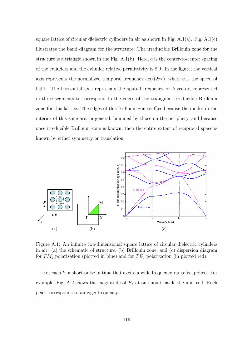
square lattice of circular dielectric cylinders in air as shown in Fig. A.1(a). Fig. A.1(c)
illustrates the band diagram for the structure. The irreducible Brillouin zone for the
structure is a triangle shown in the Fig. A.1(b). Here, a is the center-to-center spacing
of the cylinders and the cylinder relative permittivity is 8.9. In the figure, the vertical
axis represents the normalized temporal frequency ωa/(2πc), where c is the speed of
light. The horizontal axis represents the spatial frequency or k-vector, represented
in three segments to correspond to the edges of the triangular irreducible Brillouin
zone for this lattice. The edges of this Brillouin zone suffice because the modes in the
interior of this zone are, in general, bounded by those on the periphery, and because
once irreducible Brillouin zone is known, then the entire extent of reciprocal space is
known by either symmetry or translation.
(a) (b) (c)
Figure A.1: An infinite two-dimensional square lattice of circular dielectric cylindersin air: (a) the schematic of structure, (b) Brillouin zone, and (c) dispersion diagramfor TMz polarization (plotted in blue) and for TEz polarization (in plotted red).
For each k, a short pulse in time that excite a wide frequency range is applied. For
example, Fig. A.2 shows the magnitude of Ez at one point inside the unit cell. Each
peak corresponds to an eigenfrequency.
119
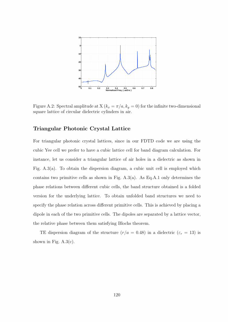
0 0.1 0.2 0.3 0.4 0.5 0.6 0.7 0.8−50
−40
−30
−20
−10
0
10
Normalized Freq. ( ωa/2πc )
Figure A.2: Spectral amplitude at X (kx = π/a, ky = 0) for the infinite two-dimensionalsquare lattice of circular dielectric cylinders in air.
Triangular Photonic Crystal Lattice
For triangular photonic crystal lattices, since in our FDTD code we are using the
cubic Yee cell we prefer to have a cubic lattice cell for band diagram calculation. For
instance, let us consider a triangular lattice of air holes in a dielectric as shown in
Fig. A.3(a). To obtain the dispersion diagram, a cubic unit cell is employed which
contains two primitive cells as shown in Fig. A.3(a). As Eq.A.1 only determines the
phase relations between different cubic cells, the band structure obtained is a folded
version for the underlying lattice. To obtain unfolded band structures we need to
specify the phase relation across different primitive cells. This is achieved by placing a
dipole in each of the two primitive cells. The dipoles are separated by a lattice vector,
the relative phase between them satisfying Blochs theorem.
TE dispersion diagram of the structure (r/a = 0.48) in a dielectric (εr = 13) is
shown in Fig. A.3(c).
120

(a) (b) (c)
Figure A.3: An infinite two-dimensional triangular lattice of air holes (r/a = 0.48) ina dielectric (εr = 13): (a) the schematic of structure. The dotted rectangle shows theunit cell which we use for bang-gap calculation, (b) Brillouin zone, and (c) dispersiondiagram for TEz polarization.
121
Bibliography
[1] N. Engheta and R. W. Ziolkowski. Metamaterials: Physics and Engineering
Explorations. John Wiley and Sons, Inc., 2006.
[2] J. B. Pendry. “Negative refraction makes a perfect lens”. Physc. Rev. Lett,
85(18):3966–3969, 2000.
[3] R. A. Shelby, D. R. Smith, and S. Schultz. “Experimental verification of a
negative index refraction”. Science, 292(77), 2001.
[4] C. Caloz and T. Itoh. Electromagnetic Metamaterials: Transmission Line Theory
and Microwave Applications. John Wiley and Sons, Inc., 2006.
[5] G. V. Eleftheriades and K. G. Balmain. Negative-Refraction Metamaterials. John
Wiley and Sons, Inc., 2005.
[6] M. Brun, S. Guenneau, and A. B. Movchan. “Achieving control of in-plane
elastic waves”. Appl. Phys. Lett., 94:061903, 2009.
[7] A. Schelkunoff and H. T. Friis. Antennas Theory and Practice. John Wiley &
Sons, NY, 1952.
[8] Said Zouhdi, Ari Sihvola, and Alexey P. Vinogradov. Metamaterials and Plas-
monics: Fundamentals, Modelling, Applications. New York: Springer-Verlag,
2008.
[9] M. Nieto-Vesperinas. “Problem of image superresolution with a negative-
refractive-index slab”. Optical Society of America, 21(4), 2004.
[10] R. Merlin. “Analytical solution of the almost-perfect-lens problem”. Applied
Physc Lett, 84(8), 2004.
[11] R. W. Ziolkowski and E. Heyman. “Wave propagation in media having negative
permittivity and permeability”. Physc. Rev. E, 64, 2001.
122

[12] C. Luo, S. G. Johnson, J. D. Joannopoulos, and J. B. Pendry. “Subwavelength
imaging in photonic crystals”. Physc. Rev. B, 68:045115, 2003.
[13] Z. Jacob, L. V. Alekseyev, and E. Narimanov. “Optical hyperlens: Far-field
imaging beyond the diffraction limit”. Optics Express, 14(18):8247, 2006.
[14] Z. Liu, H. Lee, Y. Xiong, C. Sun, and X. Zhang. “Far-field optical hyperlens
magnifying sub-diffraction-limited objects”. Science, 315:1686, 2007.
[15] T. Taubner, D. Korobkin, Y. Urzhumov, G. Shvets, and R. Hillenbrand. “Near-
field microscopy through a SiC superlens”. Science, 313(15), 2006.
[16] Manuel J. Freire and Ricardo Marqus. “Near-field imaging in the megahertz
range by strongly coupled magnetoinductive surfaces: theoretical model and
experimental validation”. Journal of Applied Phys., 100:063105, 2006.
[17] L. Wang, H. Chen, and S. Zhu. “Wave propagation inside one-dimensional
photonic crystals with single-negative materials”. Physics Letters A, 350:410–
415, 2006.
[18] D. Zheng-Gao, Z. Shi-Ning, and L. Hui. “Numerical simulations of negative-
index refraction in a lamellar composite with alternating single negative layers”.
Chinese Physics, 15:1772–1776, 2006.
[19] S. A. Ramakrishna, J.B. Pendry, D. Schurig, D. R. Smith, and S. Schultz. “The
asymmetric lossy near-perfect lens”. Journal of Modern Optics, 49(10):1747–
1762, 2002.
[20] S. A. Ramakrishna, J.B. Pendry, M.C.K Wiltshire, and W.J. Stewart. “Imaging
the near field”. Journal of Modern Optics, 2003.
[21] S. A. Ramakrishna and J. B. Pendry. “Removal of absorption and increase in
resolution in a near-field lens via optical gain”. Phys Review B, 67:201101, 2003.
[22] J. D. Kraus. “Antennas since hertz and marconi”. IEEE Trans. Antennas
Propag., Ap-33(2):131–137, 1985.
[23] C.A. Balanis. Antenna Theory. John Wiley and Sons, Inc., New Jersey, 3 edition,
2005.
[24] J. C. Maxwell. A Treatise on Electricity and Magnetism. PhD thesis, London,
UK, Oxford Univ. Press, 1873, 1904.
123

[25] J. B. Pendry, A. J. Holden, D. J. Robbins, and W. J. Stewart. “Magnetism
from conductors and enhanced nonlinear phenomena”. IEEE Trans. Microwave
Theory Tech., 47(11):2075–2084, 1999.
[26] J. B. Pendry, A. J. Holden, D. J. Robbins, and W. J. Stewart. “Low frequency
plasmons in thin-wire structures”. J. Phys. Condens. Matter, 10(22):4785–4809,
1998.
[27] C. L. Holloway, E. F. Kuester, J. Baker-Jarvis, and P. Kabos. “A double nega-
tive (dng) composite medium composed of magnetodielectric spherical particles
embedded in a matrix”. IEEE Trans. Antennas Propagat., 51(10):2596–2603,
2003.
[28] O. G. Vendik and M. S. Gashinova. “Artificial double negative (dng) media com-
posed of two different dielectric sphere lattices embedded in a dielectric matrix”.
In Proc. Of 34th European Microwave Conference, pages 1209–1212, Amsterdam,
Netherlands, 2004.
[29] L. Lewin. “The electrical constants of a material loaded with spherical particles”.
Proc. Inst. Elec. Eng., 49(65):65–68, 1947.
[30] L. Jylha, I. Kolmakov, S. Maslovski, and S. Tretyakov. “Modeling of isotropic
backward-wave materials composed of resonant spheres”. J. Appl. Phys.,
99:043102, 2006.
[31] B. J. Seo, T. Ueda, T. Itoh, and H. Fetterman. “Isotropic left handed material
at optical frequency with dielectric spheres embedded in negative permittivity
medium”. Appl. Phys. Lett., 88:161122, 2006.
[32] A. Taflove and S. C. Hagness. Computational Electrodynamics: The Finite-
Difference Time-Domain Method. Artech House, MA, 3 edition, 2005.
[33] H. Mosallaei and Y. Rahmat-Samii. “Broadband characterization of complex
periodic ebg structures: An fdtd/prony technique based on the split-field ap-
proach”. Electromag. J., 23(2):135–151, 2003.
[34] H. Mosallaei and K. Sarabandi. “Design and modeling of patch antenna printed
on magneto-dielectric embedded-circuit metasubstrate”. IEEE Trans. Antennas
Propagat., 55(1):45–52, 2007.
[35] E. Yablonovitch. “Inhibited spontaneous emission in solid-state physics and
electronics”. Phys. Rev. Lett., 58(20):2059–2062, 1987.
124

[36] J. D. Joannopoulos, R. D. Meade, and J. N. Winn. Photonic Crystals. Princeton,
NJ: Princeton Univ. Press, 1995.
[37] Special Issue on Electromagnetic Crystal Structures, Designs, Synthesis, and
Applications, IEEE Trans. Microwave Theory Tech., volume 47, 1999.
[38] E. Burstein and C. Weisbuch. Confined electrons and photons: New physics
and applications. In Proc. NATO Advanced Study Inst. Confined Electrons and
Photons: New Physics and Applications, Italy, July 13-26 1993. see also in Series
B: Physics. New York: Plenum, vol. 340, 1995.
[39] Ed. C. M. Soukoulis. Photonic band gap materials. In Proc. NATO Advanced
Study Inst. Photonic Band Gap Materials, Elounda, Crete, Greece, June 18-
30 1995. see also, Series E: Applied Sciences. Dordrecht, Germany: Kluwer
Academic, vol. 315, 1996.
[40] S. Enoch, G. Tayeb, and B. Gralak. “The richness of the dispersion rela-
tion of electromagnetic bandgap materials”. IEEE Trans. Antennas Propagat.,
51(10):2659–2666, 2003.
[41] P. V. Parimi, W. T. Lu, P. Vodo, and S. Sridhar. “Imaging by flat lens using
negative refraction”. Nature, 426(6965):404, 2003.
[42] D. Kajfez and P. Guilllon. Dielectric Resonators. Artech House, Inc., 1986.
[43] E. A. Semouchkina, G. B. Semouchkin, M. Lanagan, and C. A. Randall. “FDTD
study of resonance processes in metamaterials”. IEEE Trans. Microwave Theory
Tech., 53(4):1477–1487, 2005.
[44] L. Peng, L. Ran, H. Chen, H. Zhang, J. A. Kong, and T. M. Grzegorczyk.
“Experimental observation of left-handed behavior in an array of standard di-
electric resonators”. Phys. Rev. Lett., 98:157403, 2007.
[45] P. C. Waterman and N. E. Pedersen. “Electromagnetic scattering by periodic
arrays of particles”. J. Appl. Phys., 59(8), 1986.
[46] N. Engheta, A. Salandrino, and A. Al. “Circuit elements at optical frequen-
cies: Nanoinductors, nanocapacitors, and nanoresistors”. Phys. Rev. Lett.,
95(095504), 2005.
[47] A. Alu and N. Engheta. “Optical nanotransmission lines: synthesis of planar
left-handed metamaterials in the infrared and visible regimes”. J. Opt. Soc. Am.
B, 23(3):571–583, 2006.
125

[48] A. K. Iyer and G. V. Eleftheriades. “Volumetric layered transmission-line meta-
material exhibiting a negative refractive index”. J. Opt. Soc. Am. B, 23(3):553–
570, 2006.
[49] V. M. Shalaev, U. K. Chettiar W. Cai, H. K. Yuan, A. K. Sarychev, V. P.
Drachev, and A. V. Kildishev. “Negative index of refraction in optical metama-
terials”. Opt. Lett., 30(24):3356–3358, 2005.
[50] D. Korobkin, Y. Urzhumov, and G. Shvets. “Enhanced near-field resolution in
midinfrared using metamaterials”. J. Opt. Soc. Am. B, 23(3):468–478, 2006.
[51] M. S. Wheeler, J. S. Aitchison, and M. Mojahedi. “Coated nonmagnetic spheres
with a negative index of refraction at infrared frequencies”. Phys. Rev. B,
73:045105, 2006.
[52] P. A. Belov and Y. Hao. “Subwavelength imaging at optical frequencies using
a transmission device formed by a periodic layered metal-dielectric structure
operating in the canalization regime”. Phys Review B, 73:113110, 2006.
[53] X. Li, S. He, and Y. Jin. “Subwavelength focusing with a multilayered fabry-
perot structure at optical frequencies”. Phys Review B, 75:045103, 2007.
[54] A. Alu and N. Engheta. “Pairing an epsilon-negative slab with a mu-negative
slab: Resonance, tunneling and transparency”. IEEE Trans. on Antennas and
Prog., 51(10), 2003.
[55] A. Sommerfeld. Partial Differential Equations in Physics. New York: Academic
Press, 1949.
[56] Weng Cho Chew. Waves and Fields in Inhomogeneous Media. IEEE Press, 1995.
[57] E.N. Economou. “Surface plasmons in thin films”. Phys Review, 182(2), 1969.
[58] H. Mosallaei and K. Sarabandi. “Magneto-dielectrics in electromagnetics: Con-
cept and applications”. IEEE Trans. on Antennas and Prog., 52(6), 2004.
[59] D. R. Smith and D. Schurig. “Electromagnetic wave propagation in media with
indefinite permittivity and permeability tensors”. Phys. Rev. Lett., 90(7):077405,
2003.
[60] S. Maslovski, S. Tretyakov, and P. Alitalo. “Near-field enhancement and imaging
in double planar polariton-resonant structures”. Journal of Applied Phys., 96(3),
2004.
126

[61] H. Mosallaei and K. Sarabandi. “Antenna miniaturization and bandwidth en-
hancement using a reactive impedance substrate”. IEEE Trans. on Antennas
and Prog., 52(9), 2004.
[62] H. A. Wheeler. “Fundamental limitations of small antennas”. Proc. IRE,
35(12):1479–1484, 1947.
[63] L. J. Chu. “Physical limitation on omni-directional antennas,”. J. Appl. Phys.,
19:1163–1175, 1948.
[64] S. R. Best and D. L. Hanna. “A performance comparison of fundamental small-
antenna designs,”. IEEE Trans. Antennas Propag. Mag., 52(1), Feb., 2010.
[65] H. R. Stuart and A. Pidwerbetsky. “Electrically small antenna elements using
negative permittivity resonators,”. IEEE Trans. Antennas Propag., 54(6):1644–
1653, Jun., 2006.
[66] H.R. Stuart. “Bandwidth limitations in small antennas composed of negative
permittivity materials and metamaterials”. URSI General Assembly, Chicago,
2008.
[67] R. W. Ziolkowski and A. Erentok. “Metamaterial-based efficient electrically
small antennas,”. IEEE Trans. Antennas Propag., 54(7):2113–2130, Jul., 2006.
[68] CST Microwave Studio, ver. 2009.08 edition.
[69] A. D. Yaghjian and Steven R. Best. “Impedance, bandwidth, and q of anten-
nas,”. IEEE Trans. Antennas Propag., 53(4), Apr., 2005.
[70] A. D. Yaghjian. “Improved formulas for the q of antennas with highly lossy
dispersive materials”. IEEE Antennas and Wireless Propagation Letters, 5, 2006.
[71] M. Gustafsson, C. Sohl, and G. Kristensson. “Physical limitations on antennas
of arbitrary shape”. Proc. R. Soc. A, 463:2589–2607, 2007.
[72] M. Gustafsson, C. Sohl, and G. Kristensson. “Illustration of new physical bounds
on linearly polarized antennas”. IEEE Trans. Antennas Propagat., 57(5):1319–
27, 2009.
[73] A. D. Yaghjian and Howard. R. Stuart. “Lower bounds on q for dipole antennas
in an arbitrary volume”. IEEE-APS/URSI Symp., Toronto, 2010.
127
[74] A. D. Yaghjian and Howard. R. Stuart. “Lower bounds on the q of electri-
cally small dipole antennas”. accepted for publication in IEEE Trans. Antennas
Propag., 2010.
[75] H.R. Stuart. “Privately supplied computations of the shape factors for circularly
cylindrical disks and rods”. 2010.
[76] J. A. Stratton. Electromagnetic Theory. McGraw-Hill, Inc. USA, 1941.
[77] A. Sihvola. Electromagnetic Mixing Formulas and Applications. The Institution
of Electrical Engineers, London, 1999.
[78] H. Mosallaei and Y. Rahmat-Samii. “Composite materials with negative per-
mittivity and permeability properties: Concept, analysis, and characterization”.
IEEE AP-S International Symposium, Boston, MA, July 8-13, 2001.
[79] J. A. Encinar. “Design of two-layer printed reflectarrays using patches of variable
size”. IEEE Trans. Antennas Propag., 49(10):1403–1410, 2001.
[80] P.W. Hannan and M.A. Balfour. “Simulation of a phased-array antenna in
waveguide”. IEEE Trans. Antennas Propag., 13:342–353, 1965.
[81] N. Lenin and P.H. Rao. “Evaluation of the reflected phase of a patch using
waveguide simulator for reflectarray design”. Microwave and Optical Technology
Letters, 45:528–531, 2005.
[82] J. Li and N. Engheta. “Core-shell nanowire optical antennas fed by slab waveg-
uides”. IEEE Trans. Antennas Propag., 55(11):3018–3026, 2007.
[83] J. Li, A. Salandrino, and N. Engheta. “Shaping light beams in the nanometer
scale: A yagi-uda nanoantenna in the optical domain”. Physical Review B,
76:245403, 2007.
[84] U. Kreibig and M. Vollmer. Optical Properties of Metal Clusters. Springer-Verlag
Berlin Heidelberg, Germany, 1995.
[85] A. Alu and N. Engheta. “Polarizabilities and effective parameters for collec-
tions of spherical nanoparticles formed by pairs of concentric double-negative,
single-negative, and/or double-positive metamaterial layers”. Journal of Applied
Physics, 97:094310, 2005.
128

[86] H. Rajagopalan, Y. Rahmat-Samii, and W.A. Imbriale. “RF MEMS actuated
reconfigurable reflectarray patch-slot element”. IEEE Trans. Antennas Propag.,
56(12):3689–3699, 2008.
[87] S. Ghadarghadr, Z. Hao, and H. Mosallaei. “Plasmonic array nanoantennas
on layered substrates: modeling and radiation characteristics”. Optics Express,
17(21):18556–18570, 2009.
[88] L. Novotny and B. Hecht. Principles of Nano-Optics. Cambrdige University
Press, United Kingdom, 2006.
[89] P. Muhlschlegel, H.J. Eisler, O. J. F. Martin, B. Hecht, and D. W. Pohl.
Resonant optical antennas. Science, 308:1607–1609, 2005.
[90] J. Aizpurua, G. W. Bryant, L. J. Richter, and F. J. G. de Abajo. Optical
properties of coupled metallic nanorods for field-enhanced spectroscopy. Physc.
Rev. B., 71:235420, 2005.
[91] L. Novotny. Effective wavelength scaling for optical antennas. Physc. Rev. Lett.,
98:266802, 2007.
[92] N. Engheta. Circuits with light at nanoscales: Optical nanocircuits inspired by
metamaterials. Science, 317:1698, 2007.
[93] A. Ahmadi, S. Ghadarghadr, and H. Mosallaei. An optical reflectarray nanoan-
tenna: The concept and design. Optics Express, 18(1):123–133, 2010.
[94] A. Femius Koenderink. Plasmon nanoparticle array waveguides for single photon
and single plasmon sources. Nano Lett., 9(12):4228–4233, 2009.
[95] V. M. Shalaev. Optical negative-index metamaterials. Nature Photon., 1:41–48,
2007.
[96] A. Ahmadi, S. Saadat, and H. Mosallaei. Resonance and Q performance of
ellipsoidal eng subwavelength radiators. to be appeared in IEEE Trans. Antennas
Propag, 2010.
[97] T. H. Taminiau, F. D. Stefani, and N. F. van Hulst. Enhanced directional
excitation and emission of single emitters by a nano-optical yagi-uda antenna.
Optics Express, 16(14):10858–10866, 2008.
129

[98] M. A. Ordal, L. L. Long, R. J. Bell, S. E. Bell, R. R. Bell, R. W. Alexander,
Jr., and C. A. Ward. Optical properties of the metals al, co, cu, au, fe, pb, ni,
pd, pt, ag, ti, and w in the infrared and far infrared. Appl. Opt., 22:1099–1120,
1983.
[99] S. Uda. “Wireless beam of short electric waves”. J. IEE. (Japan), pages 273–282,
1926. pp. 1209-1219, 1927.
[100] H. Yagi. “Beam transmission of ultra short wave”. Proc. IRE, 26:715–741.
Re-printed in Proc. IEEE, vol. 72, 634-645, 1984.
[101] John L. Volakis. Antenna Engineering Handbook. McGraw-Hill, NY, 4th edition,
2007.
[102] E. F. Schubert Dexian Ye T.-M. Lu J.-Q. Xi, Jong Kyu Kim and Shawn-Yu
Lin. Very low-refractive-index optical thin films consisting of an array of sio2
nanorods. Opt. Lett., 31(5), 2006.
130