metal thin film stiffness extraction technique for surface
TRANSCRIPT

The University of Maine The University of Maine
DigitalCommons@UMaine DigitalCommons@UMaine
Electronic Theses and Dissertations Fogler Library
Fall 12-21-2018
Metal Thin Film Stiffness Extraction Technique for Surface Metal Thin Film Stiffness Extraction Technique for Surface
Acoustic Wave Filters Acoustic Wave Filters
Travis R. Weismeyer University of Maine, [email protected]
Follow this and additional works at: https://digitalcommons.library.umaine.edu/etd
Part of the Acoustics, Dynamics, and Controls Commons, Other Electrical and Computer Engineering
Commons, Other Engineering Science and Materials Commons, Other Materials Science and Engineering
Commons, Other Mechanical Engineering Commons, and the Signal Processing Commons
Recommended Citation Recommended Citation Weismeyer, Travis R., "Metal Thin Film Stiffness Extraction Technique for Surface Acoustic Wave Filters" (2018). Electronic Theses and Dissertations. 3146. https://digitalcommons.library.umaine.edu/etd/3146
This Open-Access Thesis is brought to you for free and open access by DigitalCommons@UMaine. It has been accepted for inclusion in Electronic Theses and Dissertations by an authorized administrator of DigitalCommons@UMaine. For more information, please contact [email protected].

METAL THIN FILM STIFFNESS EXTRACTION TECHNIQUE FOR SURFACE
ACOUSTIC WAVE FILTERS
By
Travis Weismeyer
B.S. University of Maine, 2016
A THESIS
Submitted in Partial Fulfillment of the
Requirements for the Degree of
Master of Science
(in Electrical Engineering)
The Graduate School
The University of Maine
December 2018
Advisory Committee:
Mauricio Pereira da Cunha, Professor of Electrical Engineering, Co-Advisor
John Vetelino, Professor of Electrical Engineering, Co-Advisor
Nuri Emanetoglu, Associate Professor of Electrical Engineering

ii
© 2018 Travis Weismeyer

METAL THIN FILM STIFFNESS EXTRACTION TECHNIQUE FOR SURFACE
ACOUSTIC WAVE FILTERS
By
Travis Weismeyer
Thesis Co-Advisors: Dr. Mauricio Pereira da Cunha and Dr. John Vetelino
An Abstract of the Thesis Presented
in Partial Fulfillment of the Requirements for the
Degree of Master of Science
(in Electrical Engineering)
December 2018
Accurate knowledge of the surface acoustic wave (SAW) properties propagating at the
surface of a piezoelectric substrate with thin films, electrodes or temperature compensated films,
is critical in SAW filter design to meet the target frequency response, power durability and
performance prior to device fabrication. While reliable material constants exist for substrates
such as LiNbO3 used in SAW filters, the absolute elastic constants associated with operational
thin films used for electrodes or temperature compensation do not exist. Although the bulk
values of the constituent materials are known, the composite film/substrate properties are
difficult to predict since they depend strongly on film deposition parameters, substrate type, and
orientation.
This work investigates a method for evaluating the effective stiffness of a composite thin
metal film by assuming an equivalent isotropic film model for an electron-beam evaporated Cu-
based thin film on a crystal substrate close to the 128°-Y cut LiNbO3, Euler angles (φ, θ, ψ) =
(0°, 38°, ψ). Two orientations on the same crystal cut were used, ψ = 0° and ψ = 53°, where the
53° orientation provided an alternative sensitivity to shear-type waves, thus allowing the unique

determination of the effective isotropic thin film elastic constants, C11 and C44, through a reverse
computational procedure while considering the error propagation from physical measurement
uncertainty. SAW delay lines in the range of 550 to 900 MHz were fabricated with and without
metal film on the delay path on a single wafer, with multiple identical devices dispersed over the
wafer and multiple wafers used for statistical analysis. The metallized SAW velocities for each
device wavelength were measured using differential delay lines with the same interdigital
transducer configuration to account only for the SAW propagation in the layered delay path. The
obtained results show promise for using a single wafer cut on LiNbO3 to characterize metal thin
films to be used for SAW filter design simulations.

iii
DEDICATION
This thesis is dedicated to my friends, my family, and most of all my folks.

iv
ACKNOWLEDGEMENTS
The author would like to acknowledge the Laboratory for Surface Science and
Technology (LASST) and University of Maine’s Electrical Engineering department’s dedicated
faculty and students for their support throughout the author’s time at the University. Notably the
author’s advisors Dr. Mauricio Pereira da Cunha and Dr. John Vetelino, and advisory committee
member Dr. Nuri Emanetoglu.
The author would like to thank Qorvo Inc. for supporting this work and the faculty who
have helped make this project possible. Notably the Qorvo employees Mark Gallagher and
Shweta Virupakshi for the design of the device mask, Jason McGann, Patrik Rath and Sebastian
Huebner for their ideas and contributions to the project, Tom Moonlight for coordination of the
fabrication process, and the project supervisors Jan Kuypers and Robert Aigner.

v
TABLE OF CONTENTS
DEDICATION ............................................................................................................................... iii
ACKNOWLEDGEMENTS ........................................................................................................... iv
LIST OF TABLES ........................................................................................................................ vii
LIST OF FIGURES ..................................................................................................................... viii
1. INTRODUCTION ................................................................................................................... 1
1.1. Background ................................................................................................................... 1
1.2. Previous Work .............................................................................................................. 2
1.3. Goal and Objectives ...................................................................................................... 7
1.4. Organization of Thesis .................................................................................................. 9
2. THIN FILM SAW PROPAGATION AND STIFFNESS EXTRACTION ........................... 10
2.1. Effect of an Isotropic Layer on SAW Properties ........................................................ 10
2.1.1. SAW Propagation with a Thin Film Layer .............................................. 10
2.1.2. Sensitivity of SAW Velocity to Varying Metal Film Parameters ............ 13
2.2. Constant Extraction Using Generated Dataspace ....................................................... 16
2.2.1. Interpolation of C11 and C44 ..................................................................... 17
2.2.2. C11 vs. C44 with SAW Velocity Uncertainty and Film Parameter
Variations .............................................................................................................. 19
2.3. Consequence of Isotropic Constant Extraction for Transverse Isotropic Thin
Film ................................................................................................................................... 23
2.3.1. Crystal Structure of Copper Thin Films ................................................... 23
2.3.2. Isotropic Elastic Constant Extraction Using Transverse Isotropic
Velocity Calculation ............................................................................................. 25

vi
3. EXPERIMENTAL SETUP .................................................................................................... 27
3.1. Description of SAW Delay Line Test Structures ........................................................ 27
3.2. Film Height and Density Metrology ........................................................................... 31
4. DATA ANALYSIS OF SAW PROPAGATION MEASUREMENTS ................................. 36
4.1 Signal Processing ........................................................................................................ 36
4.1.1. Data Quality Assessment and Windowing Bandwidth ............................ 39
4.1.2. Group Velocity Determination ................................................................. 45
4.1.3. Phase Velocity and Center Frequency Determination ............................. 52
4.2 Results of C11 vs. C44 Extraction ................................................................................. 63
5. CONCLUSION ...................................................................................................................... 73
5.1. Summary ..................................................................................................................... 73
5.2. Contributions............................................................................................................... 74
5.3. Future Work ................................................................................................................ 74
REFERENCES ............................................................................................................................. 76
APPENDIX: SAW PROPAGATION THEORY AND MATRIX METHOD ............................. 80
BIOGRAPHY OF THE AUTHOR ............................................................................................... 96

vii
LIST OF TABLES
Table 2-1 Computed elastic constants with input simulated velocity ........................................... 19
Table 2-2 Result of constant extraction simulation ...................................................................... 23
Table 3-1 Design periodicity for IDTs and corresponding excitation frequency ......................... 28
Table 3-2 Summary of profilometry and AFM thickness measurements ..................................... 34
Table 3-3 Summary of film thickness and density ....................................................................... 35
Table 4-1 Results of measured free surface phase velocity .......................................................... 59
Table 4-2 Determined elastic constants compared to accepted isotropic Cu constants ................ 68
Table A-1 Adopted Voigt notation ............................................................................................... 81

viii
LIST OF FIGURES
Figure 2-1 Phase velocity vs. hf for Cu film on 128°-Y cut LiNbO3 ........................................... 13
Figure 2-2 Phase velocity sensitivity to C11 for Cu film at different frequencies......................... 14
Figure 2-3 Phase velocity sensitivity to varying C44 for different orientations ............................ 15
Figure 2-4 Phase velocity sensitivity to C11 with varying frequency for both orientations .......... 15
Figure 2-5 Phase velocity sensitivities to C44 with varying frequency for both orientations ....... 16
Figure 2-6 Sensitivity curves for ψ = 53° orientation and input phase velocity ........................... 17
Figure 2-7 C11 vs. C44 of possible Cu film parameters at 600 MHz with ψ = 0° as the solid
blue line and ψ = 53° as the dashed red line ................................................................................. 18
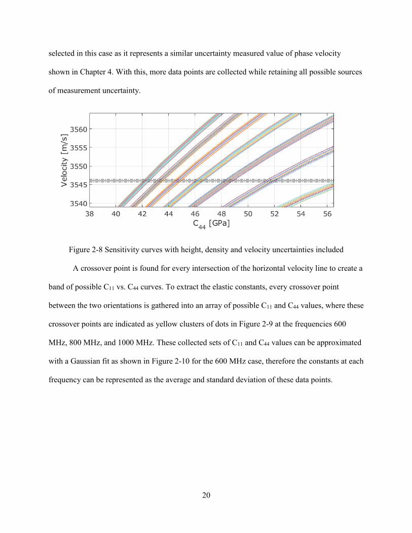
Figure 2-8 Sensitivity curves with height, density and velocity uncertainties included ............... 20
Figure 2-9 C11 vs. C44 for 600 MHz, 800 MHz, and 1000 MHz .................................................. 21
Figure 2-10 Histogram of collected C44 and C11 crossover points................................................ 21
Figure 2-11 Resulting average C44 and C11 showing standard deviation for each frequency....... 22
Figure 2-12 C11 versus frequency for transverse isotropic film .................................................... 26
Figure 2-13 C44 versus frequency for transverse isotropic film .................................................... 26
Figure 3-1 Differential delay line configuration with a thin film between the IDTs .................... 27
Figure 3-2 Mask layout of F0600D0800FU delay line ................................................................. 29
Figure 3-3 Mask layout of all devices on one die ......................................................................... 30
Figure 3-4 100x microscopic view of F0750D1000MU device ................................................... 31
Figure 3-5 Density versus thickness using determined density-thickness product ....................... 33
Figure 4-1 Flow chart for signal processing procedure ................................................................ 38
Figure 4-2 Raw frequency responses for device F0600D1000 ..................................................... 40
Figure 4-3 Different sinc2 fittings to raw data sample .................................................................. 40

ix
Figure 4-4 Normalized β versus fitting range below peak ............................................................ 41
Figure 4-5 Windowing 10β for device F0600D1000 .................................................................... 42
Figure 4-6 Time response of the three delay lines for F0600FU devices ..................................... 43
Figure 4-7 Example of three-point peak in time domain .............................................................. 44
Figure 4-8 Normalized time delay for each delay line of the F0600FU devices .......................... 45
Figure 4-9 Cross-correlated signal between two delay lines with the delay time indicated ......... 46
Figure 4-10 Group velocity versus frequency window bandwidth using (a) maximum peak
difference and (b) cross-correlation for the F0600FU devices ..................................................... 47
Figure 4-11 Group velocity versus frequency window bandwidth using (a) maximum peak
difference and (b) cross-correlation for the F0900FU devices ..................................................... 48
Figure 4-12 PSAW mode in device F0800D1000MR .................................................................. 49
Figure 4-13 Time domain response of F0800D0600MR device with increasing windowing
bandwidth ...................................................................................................................................... 49
Figure 4-14 Group velocity versus windowing bandwidth for F0800MR devices ...................... 50
Figure 4-15 FWHMs of time response of F0600D0600FU device .............................................. 51
Figure 4-16 Resulting transfer function after time-gating of F0600D0600FU device ................. 51
Figure 4-17 Procedure for calculating phase velocity from group velocity ................................. 53
Figure 4-18 Phase difference between each pair of delay lines for F0600FU devices with
the zero-phase point indicated by the dashed line ........................................................................ 55
Figure 4-19 Center frequency f0 versus time gate width and windowing bandwidth ................... 56
Figure 4-20 Zero-phase frequency fm versus time gate width and windowing bandwidth ........... 56
Figure 4-21 Phase difference showing possibility of two fm values ............................................. 58
Figure 4-22 Measured phase velocities for free surface ψ = 0° orientation ................................. 58

x
Figure 4-23 Measured phase velocities for free surface ψ = 53° orientation ............................... 59
Figure 4-24 Measured group velocities along with group and phase velocity polynomials
for ψ = 0° orientation .................................................................................................................... 62
Figure 4-25 Measured group velocities along with group and phase velocity polynomials
for ψ = 53° orientation .................................................................................................................. 63
Figure 4-26 C11 vs. C44 for 750 MHz device configuration with ψ = 0° as the blue lines and
ψ = 53° as the red lines ................................................................................................................. 64
Figure 4-27 Histogram of collected cross-over points for C11 and C44......................................... 65
Figure 4-28 C11 versus device frequency ...................................................................................... 66
Figure 4-29 C44 versus device frequency ...................................................................................... 66
Figure 4-30 Uncertainty of elastic constants versus device frequency ......................................... 67
Figure 4-31 750 MHz device with larger thickness measurement uncertainty ............................ 69
Figure 4-32 C11 error bars for larger thickness uncertainty .......................................................... 69
Figure 4-33 C44 error bars for larger thickness uncertainty. ......................................................... 70
Figure 4-34 Percent error in elastic constants for larger thickness uncertainty. ........................... 70
Figure 4-35 Simulation vs. measurement for both orientations using determined constants
using the thickness 2649 3.64 Å ................................................................................................ 71
Figure 4-36 Simulation vs. measurement for both orientations using determined constants
using the thickness 2650.1 10.4 Å ............................................................................................. 71
Figure A-1 Boundary condition function for free surface 128°-Y cut LiNbO3 ............................ 94

1
CHAPTER 1
INTRODUCTION
1.1. Background
Acoustic wave devices have earned their place in many contemporary applications, such
as cellular phones, due to their advantages in cost, performance, and size. Cell phones require
filtering of the transmitted and received signals to accurately present the desired communicated
information and exclude unwanted interference and noise. Different frequency ranges, or bands,
are required in modern telecommunication systems to separate numerous simultaneous phone
calls and exchanges of data and address different systems throughout the world. Better filters,
with lower losses, better reflection rates and sharper shape-factors are necessary to separate these
signals to handle the growing quantity of wireless communications and increasing data rates that
exist in the modern world. Since cell phones are portable, operate on low power, and are
handheld, acoustic wave devices have been the technology of choice to fulfill the above listed
requirements.
Acoustic wave filters can be employed using either surface acoustic wave (SAW) or bulk
acoustic wave (BAW) devices, which fundamentally require metal transducers on piezoelectric
material for acoustic wave excitation. The design and operation of a SAW filter is based on the
parameters of the substrate and thin film materials due to their effect on the SAW velocity,
therefore knowledge of the material’s electrical and mechanical properties is necessary to predict
performance, design, and operate the acoustic wave-based filters.
The common thin films used on top of the piezoelectric substrates include materials that
are metal, dielectric, and even piezoelectric, depending on the application. Dielectric and
piezoelectric films are used for temperature compensation and transduction waveguiding

2
functions in SAW devices respectively, however, as mentioned, metal transducers are required in
all acoustic devices as electrodes used in the conversion of electric signals to acoustic signals.
SAW devices require specific transducer finger patterns to achieve the desired response, hence,
the properties of the transducer electrodes are very important in optimization process of SAW
filter design.
Due to the nature of thin film deposition and fabrication, their acoustic properties do not
match bulk material properties of the material. Therefore, if one uses bulk properties it is
difficult to predict the impact of these thin films that are of hundreds of nanometers thick on a
SAW filter response. This justifies the need to characterize the acoustic properties of thin film
materials, particularly their stiffness parameters, which are of first order importance to the
performance of SAW filters. Metal thin film stiffness properties are of interest due to their
influence on the SAW velocity and reflectivity, and thus on the SAW device design and
performance.
1.2. Previous Work
Practical SAW devices did not begin to see widespread use until the advent of the
interdigital transducer (IDT) in 1965 [1], replacing the primitive wedge and comb transducer
configurations, and additionally being a notable substitute for physically large LC-circuits and
waveguide structures. The deposition techniques for IDTs were adopted from semiconductor
fabrication processes and take the form of interdigital fingers with opposite polarity.
SAW devices began seeing use as intermediate frequency (IF) filters starting in the late
seventies for television due to convenient size and relatively simple design [2]. Presently,
numerous long-term evolution (LTE) wireless communication frequency bands exist from
around hundreds of MHz to above one GHz [3], hence frequency-division duplexers using SAW

3
[4] and BAW [5] filter technology are utilized over the LTE range to separate transmitted (TX)
and received (RX) signals.
There are a few differences between SAW and BAW filters with respect to their
performance and cost [6], and the competition between the two technologies is sustained by the
advantages each one brings. BAW filter technology is relatively new and was introduced at the
turn of the twenty-first century for practical applications, whereas SAW filter technology has
been developing since the late 1960s. BAW filters are favored over SAW for frequencies higher
than 1.5 GHz, and are typically configured as a Film Bulk Acoustic Resonator (FBAR) or a
Solidly Mounted Resonator (SMR) [7]. These configurations require the use of thin films,
primarily piezoelectric films with metal electrodes for excitation. BAW resonators are used as
frequency-control components in communication systems, military applications, and sensors, and
are implemented through lateral-field excitation (LFE) and transverse-field excitation (TFE)
transducer designs [8][9][10].
Despite both SAW and BAW requiring thin films of some kind, they behave differently
when it comes to acoustic wave propagation, and therefore must be characterized individually.
One particularly useful attribute of SAW propagation is the ability to probe or perturb the wave
on the surface at any point, thus resulting in their use in various sensing applications, such as in
temperature, high-temperature strain [11], and chemical gas sensors, which take advantage of
thin film overlays. SAW-based sensors involve monitoring the change of a SAW velocity, phase,
or delay by correlating it to the alteration at the surface of the substrate and/or thin film overlay
with the detection of a foreign gas or physical property using perturbation theory [12], or
boundary and/or finite element methods.

4
SAW devices require anisotropic materials that exhibit piezoelectric behavior, a
phenomenon through which the electromechanical waves can be electrically excited,
manipulated, and detected. This allows for the excitation of a SAW through an electric source,
which is done typically by applying an RF signal to metal interdigital transducers (IDTs) that are
deposited on the surface with a prescribed finger pattern. When the IDT fingers are properly
designed using the correct phase velocity and in accordance to the desired frequency response,
the specific SAW devices can be realized, usually as delay lines and resonators.
SAW devices require the use of metal interdigital transducers IDTs to excite an acoustic
signal from an applied RF signal by means of the piezoelectric effect. The elastic properties,
thickness, and density of the metal electrodes, or any thin film overlay on a propagation path,
directly affect the phase velocity of a surface acoustic wave (SAW) [13]. Accurate simulation of
SAW devices, such as filters, require knowledge of the material parameters of the substrate,
electrodes, and any other overlay material involved, such as a temperature-compensating oxide
layers for example. Hence, the characterization of thin film material properties plays an
important role in performing SAW device modelling and simulation such as boundary-element
methods (BEM) and finite-element methods (FEM), and for comparison with SAW device
experimental results [14]. The deposited film properties and microstructure heavily rely on
various deposition parameters, such as temperature [15] and substrate material [16] and thin film
deposition conditions, therefore characterizing specific films used in a fabrication process is a
desirable tool.
Common piezoelectric substrates for SAW filters include quartz, LiNbO3, and LiTaO3
due to their favorable properties for SAW devices, which include electromechanical coupling,
existence of low diffraction orientations, and temperature compensated orientations [17]. Various

5
metal electrode materials are used depending on application, however aluminum is the most
common IDT material, although it suffers from irreversible microstructural damage due to
acoustomigration effects after prolonged moderate RF power [18][19]. Copper-based alloys have
seen increased use in recent years as metal grating reflectors in IF filters due to copper’s larger
mechanical reflectivity than Al, thus increasing performance [20]. Additional titanium barrier
layers above and below the Cu film have been demonstrated to increase the temperature stability
[21]. The increased experimentation with different types of IDT metals and alloys influences the
need for reliable knowledge of electrode properties.
Dielectric or piezoelectric thin film overlays, such as SiO2 or ZnO respectively, are also
used for temperature compensated SAW devices [22] [23] [24], including zero-temperature drift
devices [25]. Additionally, piezoelectric films such as AlN can be used to increase performance
of reduced piezoelectric coefficients or non-piezoelectric substrates, such as silicon [26]. These
various uses for thin films for SAW applications give rise of the need for acoustic wave thin film
material properties characterization. Most notably the determination of the stiffness parameters
for films are of first order importance particularly for metal films.
Acoustic waves have been used previously as a method to characterize thin film stiffness.
Various techniques using methods to excite acoustic waves have been used such as pulsed-laser
generation [27], Brillioun spectroscopy [28], and destructive processes such as nanoindentation
[29]. The attraction of using SAW delay lines to measure SAW acoustic propagation at a
substrate-film interface is that firstly, the SAW mode is used for such characterization. Only the
RF transfer characteristics are required, so that wafer measurements and thus thin film
characterization can be performed quickly by processing the SAW responses. SAW differential
delay lines utilize identical device configurations fabricated at different delay path lengths to

6
cancel out the effects of the IDTs by isolating the SAW on the substrate-film system while
ignoring the degrading effects of the IDTs.
Through measurement of the SAW propagation properties in a layered system, it is
possible to extract the elastic parameters of the layer material under question. Perturbative
techniques monitoring the fractional change in phase velocity have been used to characterize thin
films for sensor applications [30]. For films that are within 10% of the wavelength, perturbation
theory is a reasonable approximation to determine isotropic stiffness parameters, however for
thicker films, the perturbation equations become quickly unreliable [31]. The phenomenological
determination of the elastic coefficient thin film constants can be performed by solving an
inverse parameter problem using a numerical SAW velocity computational routines, such as
Adler’s matrix method [32] or boundary- or finite-element methods (BEM or FEM) [33].
Many thin films can be effectively modeled as an isotropic material due to polycrystalline
and/or amorphous structures. Isotropic films are described by only two independent elastic
constants. An isotropic thin film stiffness extraction procedure using SAW delay lines has been
demonstrated as early as 1983 by Jelks and Wagers [34] to characterize Al and Mo films on
128°-Y cut LiNbO3 by minimizing a least squares error between the measured and simulated
phase velocities. A later study by Ruile and Meier showed isotropic Al thin films with a thin
aluminum-oxide layer being characterized using least squares fitting by taking into account the
wave propagation in both the Al and thin oxide layer [35]. Further developments for isotropic
film stiffness characterization was made by Makarov et al [36] in 1995 by studying the error
minimization between various possible C11 and C12 values, where two different surface
orientations were additionally used to minimize the possible range of coefficients. Gallimore et
al [37] utilized the crossover points of C11 and C44 between two crystal orientations, however the

7
uncertainty in velocity measurements provided large uncertainty of 48% variation for C44 and
12% for C11. A more recent technique for thin film elastic constant extraction using SAWs and
inverse FEM simulations has been done by Knapp et al [38]. The technique was applied to the
characterization of metallic and SiO2 thin films.
Among the previously mentioned techniques to characterize thin film stiffness
coefficients, the determination of the acoustic wave velocity for the substrate-film system and the
inverse parameter extraction based on the processed SAW velocity measured data is required.
1.3. Goal and Objectives
The goal of this work is to develop and investigate a numerically quick and effective
procedure to extract the stiffness coefficients C11 and C44 of an assumed isotropic thin film for
use in SAW filters. This calls for the extraction of the referred stiffness coefficients using SAWs
themselves, and the SAW group velocity must be measured of the thin film system. Once the
SAW group velocity is measured, the phase velocity is extracted, the film thickness and density
are measured, and then the elastic constants can be determined.
The surface of deposition and deposition temperature are factors known to influence the
thin film growth microstructure characteristics of polycrystalline metals [15][16], and thus
affecting the thin film elastic coefficients. Therefore, it is ideal to characterize a single film on a
single crystal cut using the same fabrication process to ensure that the film of interest varies as
little as possible across samples.
The substrate under investigation in this work is LiNbO3, with a cut very close to 128°-Y
Euler angle orientations of (0°, 38°, 0°) and (0°, 38°, 53°). Since a difference in C11 and C44
sensitivities to SAW phase velocity has been observed through simulations, the two orientations
are utilized to extract the unique isotropic elastic constants of the Cu-based thin film. The two

8
different rotations will be referred to here as the ψ = 0° and ψ = 53° orientations, or unrotated
and rotated, respectively. The constants used for the LiNbO3 substrate in the SAW velocity
simulations are from [39], which assumes a constant room temperature of 26° C.
The thin film is an electron-beam deposited Cu-based multilayered structure, with a
titanium barrier layer to confine Cu diffusion into the substrate [21]. The Cu film is nominally
2500 Å and the whole multilayer structure will be modelled as a single isotropic layer with two
independent elastic constants C11 and C44. Losses of the film are assumed negligible and thus the
film constants will be real. An effective density of the multilayer stack, measured by physical
profilometry and atomic force microscopy (AFM) thickness measurements using specific
structures designed on the mask, and mass measurements before and after the deposition of the
film, will be used in the constant extraction procedure with the measurement error propagated.
The SAW velocities are measured using delay line devices, which were designed to
excite SAWs in the range of 600 MHz to 1000 MHz with specific devices for both surface
orientations. A signal processing algorithm is used to extract the SAW group velocities from the
measured group delay between three delay line length configurations of the same IDT pitch. The
SAW phase velocity is estimated through polynomial fitting of the group velocity and then
corrected using the measured delay line phase information.
Once the phase velocities are extracted from measurement, the values are compared
against a dataset of computed SAW phase velocities using the Adler matrix method computation
routine [40]. A solution of the isotropic constants with respective uncertainties is found using the
various intersecting points between the ψ = 0° and ψ = 53° LiNbO3 orientations.

9
1.4. Organization of Thesis
This work outlines the extraction of SAW velocities on the selected orientations using
differential delay line measurements, which are then used to compute the elastic constants C11
and C44 of the film under investigation. The details on the signal processing procedure used on
the measured RF data to find the SAW velocities will be detailed, along with the computational
procedure to determine the stiffness coefficients.
A background in SAW propagation theory is briefly covered in Chapter 2 to formulate
the process used to simulate SAW phase velocities with a thin film overlay. The properties of the
SAW phase velocity will be studied with changes in film parameters such as stiffness, density,
and thickness, and a simulation of the extraction procedure will take place. A description of the
delay lines designed, fabricated and used to measure SAW velocities and the experimental data
acquisition setup, including the thin film metrology, is covered in Chapter 3. Chapter 4 analyzes
the experimental data and describes the procedure used to determine the SAW group and phase
velocities of the delay lines. The SAW phase velocity results obtained are then used to determine
the elastic constants C11 and C44 by reverse calculation using the measured physical parameters
of the film, i.e. the thickness and density. The thesis concludes with Chapter 5 to provide a
summary of the obtained results and to support future work regarding the extraction procedure,
and implications.

10
CHAPTER 2
THIN FILM SAW PROPAGATION AND STIFFNESS EXTRACTION
2.1. Effect of an Isotropic Layer on SAW Properties
A method to calculate the SAW velocity for a thin film isotropic layer deposited on a
piezoelectric substrate must be implemented to obtain, in conjunction with measurements, the
elastic constants associated with the isotropic thin film. For a given crystallographic orientation
of the piezoelectric substrate, the change in the SAW velocity is dependent on the properties of
the film, namely the thickness, density, and elastic constants. Where the sensitivity of the
velocity to these values given a certain crystal orientation is important to extract the elastic
properties of the film in question. This section outlines the theory of SAW propagation and
subsequently shows the effect that a metal thin film and its varying parameters has on the SAW
velocity.
2.1.1. SAW Propagation with a Thin Film Layer
To calculate the SAW velocity for a given material with or without a layered stack of
materials, knowledge of the materials’ acoustic properties is required. Namely, the elastic
stiffness, the piezoelectric, and the dielectric permittivity tensors, denoted as 𝑪, 𝒆 and 𝜺
respectively, along with the density 𝜌 must be known for all materials in the structure. The
substrate orientation along which the SAW propagates in the case of an anisotropic substrate
must be specified, and in this work the substrate orientation will be expressed in terms of the
Euler angles φ, , and ψ or Euler angles (φ, , ψ). Using these angles, the previously mentioned
tensors in matrix notation are rotated to align with the direction of SAW propagation [41]. The
method used here for calculating SAW velocities is Eric Adler’s matrix method [42], where a
brief review of SAW propagation theory and the matrix method can be found in the appendix.

11
For a bare substrate, the SAW propagation theory assumes no mass loading on the
surface. However, in the case of a layered system, the surface of the substrate is now mass-
loaded with a layer and the calculation procedure of the SAW velocity must consider this effect,
along with the influence of the layer’s material properties. A thin film layer on top of the surface
of a substrate can be represented by means of a transmission matrix, which describes how the
SAW fields translate from the interface of the layer-substrate to the interface of the thin film with
air. Since the layered system introduces dispersive behavior, the transmission matrix is a
function of frequency. The final SAW velocity solution will change depending on frequency and
height of the film. This section introduces the transmission matrix and describes how it can be
used to analyze layered SAW propagation.
The transmission matrix ties the SAW fields from one boundary to another. For example,
consider a SAW propagating for a piezoelectric substrate with a thin film layer of finite
thickness. The transmission matrix in Equation (2-1) describes how the fields behave in the
presence of a layer with height ℎ𝐿 and a system matrix 𝑨𝐿 containing the material constant
parameters of the thin film material.
Φ𝑇𝐿 = exp(𝑗𝜔𝑨𝐿ℎ𝐿)
(2-1)
For multiple layers, the transmission matrix for each layer can be cascaded in a total
transmission matrix. The transmission matrix allows analysis of any number of layers for SAW.
In this work, the film under investigation is modeled as a single film layer, therefore cascading
layers will not be necessary. Equation (2-1) is used to map the SAW field equations 𝝉 through
the film and can be written as

12
𝝉(𝑧 + ℎ𝐿) = exp(𝑗𝜔𝑨𝐿ℎ𝐿) 𝝉(𝑧) = Φ𝑇𝐿𝝉(𝑧),
(2-2)
and using the fields at the surface of the substrate, defined as 𝝉(0) = 𝑼𝑆𝑝�̅�𝑼(0),
Φ𝑇𝐿𝝉(0) = Φ𝑇𝐿𝑼𝑆𝑝�̅�𝑼(0) = 𝑩�̅�𝑼(0),
(2-3)
where 𝑩 = Φ𝑇𝐿𝑼𝑆𝑝 and 𝑼𝑆𝑝 is the eigenvector matrix of the SAW decaying partial modes
(DPM). Thus, the boundary condition functions with a layer can be expressed as:
𝑓𝑠𝑐(𝑣𝑝) = |𝑩(1: 3, : )
𝑩(8, : )| = 𝟎
(2-4)
for the short-circuit case, and
𝑓𝑜𝑐(𝑣𝑝) = |
𝑩(1: 3, : )
𝑩(4, : ) + 𝑗휀0
𝑣𝑝𝑩(8, : )| = 𝟎
(2-5)
for the open-circuit case. For the case of a metal film taken as a perfect conductor, Equation
(2-4) should be used.
Using the velocity calculation procedure described, the height of the layer can be
incrementally increased to show the change in phase velocity with different layer thicknesses or
frequencies. Since the transmission matrix is an exponential that is dependent on the product of
height and frequency, this product can be represented as a single quantity to couple height and
frequency in the calculation. A plot of the phase velocity versus the height-frequency (hf)
product in km/s is shown in Figure 2-1 for an isotropic Cu film on 128°-Y cut LiNbO3, Euler
angles (0°, 38°, 0°). The film constants used are C11 = 200.87 GPa and C44 = 47.3 GPa which
come from Hill’s average [43] of the single crystal data [44], and density of ρCu = 8960 kg/m3

13
[45]. Evidently, in addition to variation of the phase velocity with thickness and frequency, the
phase velocity changes with varying stiffness and density parameters of the film.
Figure 2-1 Phase velocity vs. hf for Cu film on 128°-Y cut LiNbO3
This work investigates two orientations for the stiffness extraction, which implies that the
velocity sensitivities to the isotropic constants C11 and C44 along these orientations are different.
The crystal cut under investigation is an orientation very close to 128°-Y Euler angle orientations
of (0°, 38°, ψ). The first orientation is unrotated, or ψ = 0°, and the second orientation is rotated
by 53°, i.e. ψ = 53°. The ψ = 53° was originally selected due to its larger coupling to the y-
component compared to the ψ = 0° orientation by approximately a factor of 8. Additionally, the
power flow angle for ψ = 53° was closest to 0° to minimize unwanted beam steering effects
while still maintaining the larger shear coupling. The difference in the shear components
between the two orientations is reflected through their differing velocity sensitivities to C11 and
C44.
2.1.2. Sensitivity of SAW Velocity to Varying Metal Film Parameters
The SAW velocity sensitivity is defined to be the change in phase velocity with respect to
a change in the parameter of choice. This can be found by varying a chosen parameter around a

14
nominal value and recalculating the phase velocity for each new value, where the rest of the
parameters are fixed. Since the layered system is frequency-dependent, different frequency
points offer different velocity sensitivities. The relative change in phase velocity to varying C11
is shown in Figure 2-2 for an isotropic 2500 Å Cu film for 500 MHz and 1000 MHz on the ψ =
0° orientation to demonstrate the difference in sensitivity curves for different frequencies. The
phase velocity sensitivity shows to increase with increasing frequency.
Figure 2-2 Phase velocity sensitivity to C11 for Cu film at different frequencies
A difference in sensitivity is desired between the two orientations to be used for the
constant extraction. This can be shown visually by varying the same constant with the same
frequency for both orientations, for example in Figure 2-3 for C44 at 1000 MHz. With these
degrees of freedom in mind, it is imperative to view how these sensitivities compare and vary
over the frequency range of the devices used for constant extraction. The phase velocity
sensitivity to C11 and C44 will be represented as δ(vp)/δ(C11) and δ(vp)/δ(C44) respectively. These
values are found from the change in velocity over the change in the elastic constant linearized
around the nominal point where the slope is quantified. A comparison of the sensitivities for both
orientations is shown in Figure 2-4 for C11 as a function of frequency.

15
Figure 2-3 Phase velocity sensitivity to varying C44 for different orientations
Figure 2-4 Phase velocity sensitivity to C11 with varying frequency for both orientations
The sensitivities to C11 vary at similar rates with increasing frequency, however different
behavior is observed for C44 sensitivities, as shown in Figure 2-5.

16
Figure 2-5 Phase velocity sensitivities to C44 with varying frequency for both orientations
Close to the 700 MHz mark, or an hf product of 0.175 km/s, the increase rate of the
sensitivity to C44 for the ψ = 0° diminishes while the ψ = 53° surpasses it and continues at a
steady rate.
Producing phase velocity sensitivity curves for varying film parameters is fundamental to
the constant extraction procedure in that they can be calculated to make a dataspace for
interpolation.
2.2. Constant Extraction Using Generated Dataspace
Due to the difference in phase velocity sensitivity to the elastic constants between the two
orientations, the basis of extracting these elastic constants involves finding a unique solution that
is valid for both orientations. For a given velocity, each orientation has an array of possible C11
and C44 values. These values can be found by computing a dataspace with a range of C11 and C44
values and interpolating the values matching the input phase velocity. A curve of possible C11
and C44 values for each orientation is generated and the crossover point indicates the elastic
constant solution.

17
2.2.1. Interpolation of C11 and C44
Multiple sensitivity curves can be precomputed for a wide array of different parameter
variations, including thickness and density as addressed later, and are compiled to cover the span
of interest, typically within approximately 30% of the starting constants. This set of data
essentially contains the velocity sensitivity information to a certain parameter and can be used to
compute a C11 vs. C44 graph for different values of velocity. The utility behind these curves
comes in when a certain velocity is known, such as a measured phase velocity. To demonstrate
this procedure, the known velocity will be the velocity resulting from a SAW simulation using
the nominal Cu film parameters mentioned in Section 2.1.1. These curves are shown for the 53°
orientation at 600 MHz in Figure 2-6, and the known velocity is indicated by the dashed line.
Each different colored curve represents different C11 values evenly spaced within ±30% of the
starting value.
Figure 2-6 Sensitivity curves for ψ = 53° orientation and input phase velocity
Obtaining the corresponding C44 to each C11 curve is a matter of interpolating the value
of C44 where the dashed velocity line crosses each point. The resulting C11 vs. C44 can be created
from each of the selected orientations and their crossover point indicates the solution, shown in

18
Figure 2-7, where the solid line is the ψ = 0° orientation and the dashed line is ψ = 53°. Each one
of these curves corresponds to the single input velocity value.
Figure 2-7 C11 vs. C44 of possible Cu film parameters at 600 MHz with ψ = 0° as the solid blue
line and ψ = 53° as the dashed red line
Each intersection of the phase velocity with one line from Figure 2-6 corresponds to one
point on a line for the C11 vs. C44 curve. The unique solution to this case is the crossover point
between the lines of Figure 2-7. The previously mentioned C11 and C44 constants for the isotropic
Cu film were input to obtain the velocities which were represented by the dashed line as in
Figure 2-6. The extracted constants at the particular frequency are obtained from the crossover
points of the C11 and C44 curves for each orientation. The accuracy of the crossover point
interpolation is tabulated for the frequencies 600 MHz, 800 MHz and 1000 MHz in Table 2-1.
The elastic constants that resulted from this procedure were within a few hundred ppm
from the constants that were used to calculate the input velocities. This minor discrepancy is
believed to be a result from the interpolation using cubic splines that takes place in finding the

19
C11 vs. C44 data points. However, as will be shown later, these small inaccuracies are a few
orders of magnitude less than the measurement uncertainty that is propagated to the solution for
the experimental setup and thus these parts-per-million (ppm) discrepancies fall into the noise of
the constant extraction procedure.
Table 2-1 Computed elastic constants with input simulated velocity
Frequency
[MHz]
Output C11
[GPa]
Difference from
input C11 [ppm]
Output C44
[GPa]
Difference from
input C44 [ppm]
600 200.756 -567 47.317 +359
800 200.984 +567 47.280 -423
1000 200.984 +567 47.280 -423
2.2.2. C11 vs. C44 with SAW Velocity Uncertainty and Film Parameter Variations
The thin film height and density are crucial parameters in determining its elastic
constants of a film due to the high phase velocity sensitivity to these parameters. To perform the
extraction for a measured film, the uncertainties in height and density measurements must be
considered. This requires an expansion of the computed dataspace to propagate the uncertainties
in film height and density measurements. That is, for every range of C11 and C44 that a velocity is
computed, an additional curve is created based on the limits of the height and density
uncertainties. Here, the height and density uncertainties are inserted as ±0.1% from the nominal
values for demonstration, as this number is similar to the actual measurement uncertainties
shown in Chapter 3. This procedure results in a cluster of lines for every step of C11 as shown in
Figure 2-8 for the ψ = 0° orientation at 600 MHz, where the phase velocity is additionally varied
by ±0.01% from its simulated value to reflect the velocity uncertainty. This value was arbitrarily
20
selected in this case as it represents a similar uncertainty measured value of phase velocity
shown in Chapter 4. With this, more data points are collected while retaining all possible sources
of measurement uncertainty.
Figure 2-8 Sensitivity curves with height, density and velocity uncertainties included
A crossover point is found for every intersection of the horizontal velocity line to create a
band of possible C11 vs. C44 curves. To extract the elastic constants, every crossover point
between the two orientations is gathered into an array of possible C11 and C44 values, where these
crossover points are indicated as yellow clusters of dots in Figure 2-9 at the frequencies 600
MHz, 800 MHz, and 1000 MHz. These collected sets of C11 and C44 values can be approximated
with a Gaussian fit as shown in Figure 2-10 for the 600 MHz case, therefore the constants at each
frequency can be represented as the average and standard deviation of these data points.

21
Figure 2-9 C11 vs. C44 for 600 MHz, 800 MHz, and 1000 MHz
Figure 2-10 Histogram of collected C44 and C11 crossover points
The standard deviations of the determined constant average decreases with frequency, as
is shown by the reduction of area of crossover points from Figure 2-9. This is due to the phase
velocity sensitivity for both constants increasing with frequency for both orientations, causing an
increase in orthogonality between each orientation. This is reflected by the decrease in standard
deviation while the average constants remain approximately the same with increasing frequency
in Figure 2-11.

22
Figure 2-11 Resulting average C44 and C11 showing standard deviation for each frequency
Since the precision increases with frequency due to the increase in orthogonality between
the orientations, it is worth employing a weighted average to extract the final values of the
stiffness coefficients. The weighted average of all the frequency results places more weight on
groups of data that have smaller standard deviation from the average value, i.e. in this case the
weight is placed more on higher frequencies. The weighted average 𝑥𝑤𝑎𝑣 is shown in Equation
(2-6), assuming the measurements are governed by a Gaussian profile [46],
𝑥𝑤𝑎𝑣 =∑𝑤𝑖𝑥𝑖
∑𝑤𝑖,
(2-6)
where 𝑤𝑖 is the weight of the ith dataset, given by the inverse variance of the measurement in
Equation (2-7).
𝑤𝑖 =1
𝜎𝑖2
(2-7)
The weighted standard deviation 𝜎𝑤𝑎𝑣 can be found using each of the corresponding
weights as in Equation (2-8),

23
𝜎𝑤𝑎𝑣 =1
√∑𝑤𝑖
.
(2-8)
The results for the constant extraction for this simulated process is shown in Table 2-2.
Table 2-2 Result of constant extraction simulation
Elastic Constant
Input Constants (Hill’s
Average [44])
Constant Extraction
Procedure Result
C11 [GPa] 200.87 200.88 1.2 GPa
C44 [GPa] 47.3 47.3 0.2 GPa
This simulation shows that this process is feasible for characterizing isotropic films and
therefore suitable for processes that can determine the thickness and density of the film and
SAW phase velocity.
2.3. Consequence of Isotropic Constant Extraction for Transverse Isotropic Thin Film
2.3.1. Crystal Structure of Copper Thin Films
In this work, the film under question is assumed isotropic to limit the determination of
stiffness to only two elastic constants. It is well known that the properties of a deposited thin film
can be vastly different from those of the bulk source material. There are three main
classifications for crystal lattice structure: crystalline (or single crystal), polycrystalline, and
amorphous. Crystalline structures have a single primitive design which is repeated throughout
the whole structure by translation and is classified by the size and shape of the primitive unit cell.
Polycrystalline materials contain many different crystalline structures orientated in random

24
directions along most directions and sometimes aligned for specific directions. Amorphous
materials are classified as having no atomic order; there is no single consistent pattern.
Amorphous films can generally be considered isotropic. Polycrystalline films can also be
considered isotropic in some cases, depending on the degree of randomness in the orientations of
the composite crystallites [45]. Films that are not isotropic are anisotropic and are categorized by
crystal structure type, including configurations such as hexagonal and cubic.
The structure of the material dictates the form of the elastic stiffness tensor. For isotropic
materials, there are two independent elastic constants that dictate all entries of the stiffness
tensor, given here in abbreviated subscript notation
𝐶 =
[ 𝐶11 𝐶12 𝐶12 0 0 0𝐶12 𝐶11 𝐶12 0 0 0𝐶12 𝐶12 𝐶11 0 0 00 0 0 𝐶44 0 00 0 0 0 𝐶44 00 0 0 0 0 𝐶44]
,
(2-9)
where 𝐶12 = 𝐶11 − 2𝐶44.
Crystalline copper, for instance, has a face-centered cubic (FCC) structure. Previous
studies suggest that vapor-deposited Cu thin films favor polycrystalline columnar structures with
dominant <111> orientations, where the size of the columnar grains is influenced by the
deposition temperature ratio to Cu’s melting point [47]. Furthermore, films with Ti underlayers
that have strong <111> components influence a likewise strong <111> component on Cu films
[48]. Other deposition methods have shown dominant <111> structures in Cu thin films and thus
suggesting transverse isotropy [49]. The stiffness tensor for a transverse isotropic material takes
the form

25
𝐶 =
[ 𝐶11 𝐶12 𝐶13 0 0 0𝐶12 𝐶11 𝐶13 0 0 0𝐶13 𝐶13 𝐶33 0 0 00 0 0 𝐶44 0 00 0 0 0 𝐶44 00 0 0 0 0 𝐶66]
,
(2-10)
where 𝐶66 =1
2(𝐶11 − 𝐶12), giving five independent elastic constants. Therefore, it is important
to consider the possibility of a transverse isotropic film and observe the implications of assuming
it is isotropic during the stiffness constant extraction.
2.3.2. Isotropic Elastic Constant Extraction Using Transverse Isotropic Velocity
Calculation
The same numerical experiment from Section 2.2.2 can be applied to the case of
velocities generated using transverse isotropic stiffness constants computed from a <111> Cu
polycrystalline structure [50]. Instead of generating the input velocities using the isotropic
constants for Cu, transverse isotropic constants are used. Those phase velocities are interpolated
on the data space consisting of possible isotropic combinations. This simulation aims to
investigate what occurs when a non-isotropic film is assumed to be isotropic.
The results of the extracting C11 and C44 using height and density uncertainties of 0.1%,
and velocity uncertainties of 0.01% are shown in Figure 2-12 and Figure 2-13.

26
Figure 2-12 C11 versus frequency for transverse isotropic film
Figure 2-13 C44 versus frequency for transverse isotropic film
It is important to note the frequency dependence of the extracted constants, meaning that
if the result of the constant extraction using this method gives rise to a noticeable frequency
dependence, then it is possible that the film is transverse isotopic. It is also worth mentioning that
C11 exhibits a decrease of approximately 17% between 600 MHz and 1000 MHz, where C44
decreases only approximately 2%. This is likely due to the smaller sensitivity of the phase
velocity to C11 with increasing frequency compared to C44.

27
CHAPTER 3
EXPERIMENTAL SETUP
3.1. Description of SAW Delay Line Test Structures
Fundamentally, SAW devices require thin film electrodes configured as inter-digital
transducers (IDTs) on piezoelectric substrates for SAW excitation. To determine the velocity of
the SAW in the free or metallized region and independently of the IDT regions, differential delay
line structures were utilized. A simple diagram of a SAW delay line setup is illustrated in Figure
3-1.
Figure 3-1 Differential delay line configuration with a thin film between the IDTs
Here, ∆𝑠 is the difference in length between the two delay line structures. Delay lines are
appropriate to measure the velocity of SAWs due to the well-defined differential propagation
path [51]. To analyze the propagation of the SAW in the presence of a metallic film on the
piezoelectric substrate requires the assumption that a given pair of adjacent devices have
identical IDTs and the only difference between the two configurations is the difference in delay
path length. This grants a view of the differential propagation path between a pair of delay lines

28
for effectively examining the properties of the differential SAW propagation path (or delay time)
without the influence of the IDTs. The differential delay paths allow the determination of the
SAW group velocity. The SAW phase velocity is then determined from the group velocity
evaluation and the phase difference between the delay line pair. A more in-depth explanation for
determining the SAW group and phase velocities is described later in Chapter 4. The phase
velocity of the layered system enables extraction of the properties of the thin film overlay when
the parameters of the substrate are assumed to be known, as discussed in Chapter 2.
The device design is based on the work of Knapp [52] to determine the phase velocity of
a free surface or metal-layered system on lithium niobate substrate and considering only the
differential delay path ∆𝑠. Split-finger interdigital transducers (IDTs) were designed to operate at
specific wavelengths, where the period of the IDTs is the wavelengths and the width of each
electrode is 1/8 of the wavelength, thus implementing the split-finger configuration. A total of
nine different IDT device periodicities were designed on the wafer mask and are shown in Table
3-1 along with their target operating frequencies.
Table 3-1 Design periodicity for IDTs and corresponding excitation frequency
Device λ
[µm]
6.335 5.83 5.4 5.02 4.69 4.397 4.136 3.902 3.69
Target
Frequency
[MHz]
600 650 700 750 800 850 900 950 1000
For each device periodicity, three delay lines were fabricated with IDT center-to-center
spacing of 600 µm, 800 µm, 1000 µm. For each device configuration, structures with both a free

29
surface and a metal layer between the sender and receiver IDTs have been designed. Since there
are two orientations, 9 pitches, 3 delay lengths per pitch, and are either free or metallized, there
are a total of 108 unique devices on a single wafer die. An example of a free-surface device is
shown in Figure 3-2.
Figure 3-2 Mask layout of F0600D0800FU delay line
Each device case has a unique identification label, shown in the bottom-left of Figure 3-2.
The first part ‘F0XXX’ specifies the device design frequency, the second part ‘D0XXX’
specifies the length of the delay in microns, and the final part denotes whether the device is free
surface (‘F’) or metallized (‘M’) and un-rotated (‘U’) or rotated (‘R’). Figure 3-2 shows the 600
MHz frequency, 800 µm delay, and un-rotated free surface, i.e. the orientation close to LiNbO3
128°-Y, corresponding to the label ‘F0600D0800FU’. This labelling system will be used
throughout this thesis for convenience when referring to a specific device case and delay line. A
set of delay lines can also be abbreviated, such as ‘F0600FU’, which includes all delay lines of
the free-surface ψ = 0° rotation 600MHz devices.

30
There are nine total sites on the wafer each with the same mask layout, giving nine
different measurements of the same device case. Each site of the wafer will be used for the
analysis of the SAW velocity. Since there are three delay line configurations per device case, the
resulting number of velocity points is 27 for each case per wafer, where a case indicates both the
pitch and whether there is a metal overlay or not. The layout of the mask is shown in Figure 3-3.
Figure 3-3 Mask layout of all devices on one die
It is noted that on the mask of the devices, each set of delay lines are adjacent to each
other. A microscopic image of a metallized device is shown in Figure 3-4.

31
Figure 3-4 100x microscopic view of F0750D1000MU device
To assess the properties of the film under question, RF measurements were made on each
device on each wafer site. The location of the probe pads is the same for each device for
automated probing, hence furthering the rapid evaluation process.
3.2. Film Height and Density Metrology
To find the elastic parameters of the film, the thickness and density, which are critical to
computing the layered SAW velocity, must be measured independently. The absolute thickness
measurements came from physical step height measurements of the film using profilometry and
atomic force microscopy (AFM). The density was determined by measuring the mass of the
wafer before and after the film was deposited and using the measured thickness and area of the
wafer to obtain the film volume. The quantity gained from the mass measurement and wafer area
gives a so-called density-thickness product, which is used with the thickness to determine the
density.
32
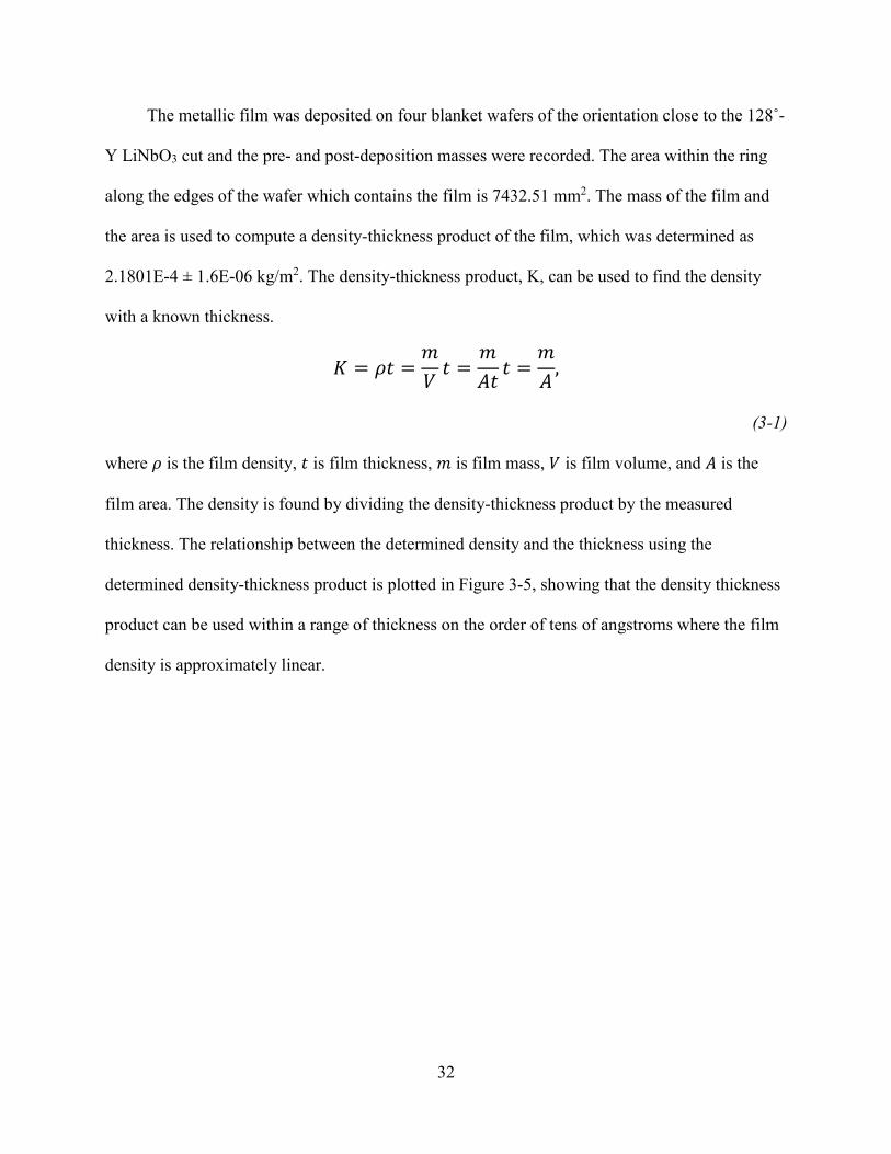
The metallic film was deposited on four blanket wafers of the orientation close to the 128˚-
Y LiNbO3 cut and the pre- and post-deposition masses were recorded. The area within the ring
along the edges of the wafer which contains the film is 7432.51 mm2. The mass of the film and
the area is used to compute a density-thickness product of the film, which was determined as
2.1801E-4 ± 1.6E-06 kg/m2. The density-thickness product, K, can be used to find the density
with a known thickness.
𝐾 = 𝜌𝑡 =𝑚
𝑉𝑡 =
𝑚
𝐴𝑡𝑡 =
𝑚
𝐴,
(3-1)
where 𝜌 is the film density, 𝑡 is film thickness, 𝑚 is film mass, 𝑉 is film volume, and 𝐴 is the
film area. The density is found by dividing the density-thickness product by the measured
thickness. The relationship between the determined density and the thickness using the
determined density-thickness product is plotted in Figure 3-5, showing that the density thickness
product can be used within a range of thickness on the order of tens of angstroms where the film
density is approximately linear.

33
Figure 3-5 Density versus thickness using determined density-thickness product
The absolute film thickness was determined using both physical profilometry and atomic
force microscopy (AFM). The thickness measurement techniques both used a physical stylus to
measure the step height of the film using dedicated structures on the mask. Profilometry was
measured using the step height of two metal rectangles that are placed at the center of each wafer
site. AFM was performed on a special fingered structure that are on each delay line structure die
to measure thickness at selected points covering a wide diameter of all the devices used for
evaluation.
The results of the physical thickness measurements are summarized in Table 3-2, where
the mean thickness and standard deviation are grouped according to metrology technique and
wafer label. Each case contains an associated number of measurement points, and the results for
the thicknesses and uncertainties used are tabulated. The mean and standard deviation of the
thickness measurements are reported independently for both the profilometry and AFM
metrologies. The final two columns report the weighted average and weighted standard deviation
resulting from all five of the shown measurement trials for both metrologies and wafers.

34
Table 3-2 Summary of profilometry and AFM thickness measurements
Metrology
Wafer
#
Measurement
Points
mean
thickness
[Å]
St.
Dev.
[Å]
%
deviation
mean per
metrology
[Å]
weighted
average
[Å]
weighted
St. Dev.
[Å]
Profilometry
A
9 2647.4 4.6 0.17%
2650.1 ±
10.5
2649 3.6
3 2647 7 0.27%
B 3 2661.3 19.9 0.75%
AFM
A 9 2671.1 15.4 0.58% 2646.7 ±
44.5 B 9 2622.2 51.2 1.95%
Since the density depends on both the measured mass and the measured thickness, the
uncertainty in the density depends on the uncertainty of both the mass and thickness. The
fractional density uncertainty is calculated by
𝛿𝜌
|𝜌|= √(
𝛿𝐾
𝐾)2
+ (𝛿𝑡
𝑡)2
,
(3-2)
where 𝐾 is the density-thickness product and 𝛿𝐾 is the uncertainty in the density-thickness
product due to the uncertainty in mass.
The X-ray fluorescence (XRF) method was also investigated in this work for the
measurement of 𝐾. The technique was applied to a pure Cu film deposited on a quartz wafer and
a thickness of approximately 2450 Å was obtained, therefore resulting in a density of
approximately 8720 kg/m3. This is a reasonable result as the density for electron-beam
evaporated Cu thin films has been reported to approach the bulk density value 8960 kg/m3 with
increasing thickness [53]. The density value is expected to be lower than the bulk value, but
never exceeded. Although XRF is useful for single-material films, it provided inconsistent

35
measurements for the multilayer Cu film under question here, and the collected data was not
used for the thin film characterization.
The film under investigation for constant extraction was weighted and the profilometry
and AFM thickness measurements were used. A summary of the height and density
measurements that are used as the inputs to the SAW velocity simulation are tabulated in Table
3-3.
Table 3-3 Summary of film thickness and density
Thickness Metrology
Profilometry + AFM
(weighted)
Profilometry only
Density-Thickness Product K [kg/m3] 2.1809E-4 ± 1.6E-06
Measured Thickness [Å] 2649 ± 3.64 2650.1 ± 10.4
Resulting Density [kg/m3] 8233 ± 13 8229.5 ± 33
Profilometry gave a more precise measurement of the film thickness than AFM, therefore
the weighted average was computed when using all the measurement points. The result of the
profilometry measurements alone are also considered.
The next chapter utilizes the experimental setup and the measured thickness and density
introduced in this chapter to determine the group and phase velocity using the RF measurements,
and to extract the stiffness coefficients C11 and C44 of the Cu-based thin film investigated.

36
CHAPTER 4
DATA ANALYSIS OF SAW PROPAGATION MEASUREMENTS
The determination of the SAW phase velocity is an essential component of the constant
extraction procedure since it is used directly in the inverse parameter problem to solve for the
stiffness parameters C11 and C44. Although the phase velocity is the desired input quantity for the
simulation, the group velocity must first be evaluated from the S21 measurements. By measuring
the time delay between one pair of delay lines and using the known physical length difference
between them from the mask design, the group velocity can be found as a function of frequency.
For the free surface, the group velocity can be used as an estimate for the phase velocity since
the propagation is non-dispersive. The estimation is then used to find the true phase velocity
using the phase response of the S21. For the metallized surface, a phase velocity estimate can be
found by fitting a polynomial to the group velocity due to the dispersion of the layered system.
This chapter outlines the determination of the group and phase velocities for a free and
metallized surface using measured S21 data of differential delay lines and subsequently uses the
phase velocity results to extract C11 and C44.
4.1 Signal Processing
The group velocity of the surface acoustic wave (SAW) can be found in terms of the
difference in transit times and differential length between a pair of delay lines, as expressed in
Equation (4-1).
𝑣𝑔 =∆𝑠
∆𝜏,
(4-1)
where ∆𝑠 is the difference in path length between one delay line and another, and ∆𝜏 is the
difference in transit time between the two analyzed delay lines. The path length difference ∆𝑠 is

37
known exactly from the device mask and is assumed constant for each case, therefore
determination of the time delay is required for each pair of delay lines to obtain the group
velocity. The time response can be obtained by performing an inverse Fast Fourier Transform
(IFFT) on the measured S21 frequency response. The transit time of the SAW from the input IDT
to the output IDT is where the magnitude peak occurs, which must be found for each delay line
to find the resulting time difference ∆𝜏 of the SAW between two different length delay lines for
both the free or metallized surface. The usage of the time difference eliminates the effects of the
transmitting and receiving IDTs on the group velocity. Evidently, the IDTs for both delay line
pairs are assumed identical, which is an important consideration for the fabricated devices and
the measured data.
The extracted transit time however is a function of the initial frequency windowing of the
raw S21 measurement data, since unwanted acoustic modes or reflections can make their way into
the time response, which may be represented by a ripple or additional passbands in the frequency
domain. One of the most common and expected source of spurious signals is the triple transit
SAW since they exist within the passband frequency range and cannot be windowed out in the
frequency domain, however they can be removed by time-gating the impulse to obtain an S21
transfer function with the ripple removed. There are other possible sources of disturbance, which
can include but are not limited to SAW reflections from other metallic structures on the wafer,
spurious bulk acoustic wave (BAW) excitation, and even additional SAW-type modes. The latter
two disturbances can sometimes be seen in the frequency domain in a separate passband. These
distortions can lead to inaccurate determination of the impulse response peak due to the
superposition of received acoustic signals in the time domain, and therefore cause uncertainty in
38
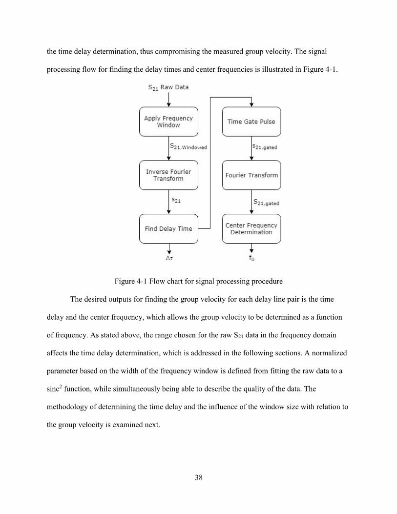
the time delay determination, thus compromising the measured group velocity. The signal
processing flow for finding the delay times and center frequencies is illustrated in Figure 4-1.
Figure 4-1 Flow chart for signal processing procedure
The desired outputs for finding the group velocity for each delay line pair is the time
delay and the center frequency, which allows the group velocity to be determined as a function
of frequency. As stated above, the range chosen for the raw S21 data in the frequency domain
affects the time delay determination, which is addressed in the following sections. A normalized
parameter based on the width of the frequency window is defined from fitting the raw data to a
sinc2 function, while simultaneously being able to describe the quality of the data. The
methodology of determining the time delay and the influence of the window size with relation to
the group velocity is examined next.

39
4.1.1. Data Quality Assessment and Windowing Bandwidth
To process the raw measured S21 data, a normalization parameter around the bandwidth
of interest is desired to normalize a definition for the frequency window bandwidth. This
involves fitting the raw data to the impulse response of a delay line, which can be approximated
as a sinc2 function [54]. The sinc2 function was parameterized using the following approximate
relation which was obtained from adjustments with the experimental data in this work:
𝐺(𝑓) = 𝐴
(
sin [
2√2(𝑓 − 𝑓𝑐)𝛽
]
2√2(𝑓 − 𝑓𝑐)𝛽 )
2
,
(4-2)
where 𝑓𝑐 is the center frequency, 𝐴 is the amplitude of the signal, and 𝛽 is a fitting parameter
approximately equal to the full-width half maximum (FWHM) bandwidth. The measured data
points are used to find the parameters which minimize the function 𝐺(𝑓) by minimizing the sum
of squared residuals
𝑆𝑆𝑟𝑒𝑠 = ∑(𝑦𝑖 − 𝐺(𝑓𝑖))2
𝑖
,
(4-3)
where 𝑦𝑖 are the points chosen for the fitted function. For the minimization problem, the
parameters 𝑓𝑐, 𝐴, and 𝛽 are initially taken from the raw data as the maximum frequency point 𝑓𝑐𝑖,
the amplitude at that frequency 𝐴𝑖, and the full-width half maximum bandwidth 𝛽𝑖, respectively.
The raw data for the 600 MHz 1000 µm delay line is shown for each of the nine wafer sites in
Figure 4-2.

40
Figure 4-2 Raw frequency responses for device F0600D1000
The number of data points from the raw data used for the sinc2 fitting are selected in
terms of dB below the peak of the passband. For example, if the fit range below peak was chosen
as 20 dB, then all the points in the passband up to 20 dB below the amplitude at the center
frequency are used as the 𝑦𝑖 inputs. An example of two ranges below the peak are shown in
Figure 4-3 to illustrate the effect on the number of input points for the free surface 600 MHz
1000 µm delay line.
Figure 4-3 Different sinc2 fittings to raw data sample
41
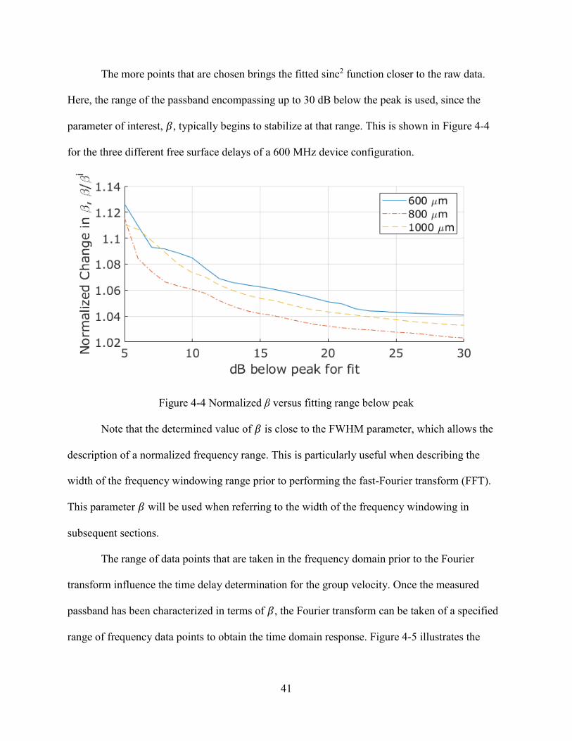
The more points that are chosen brings the fitted sinc2 function closer to the raw data.
Here, the range of the passband encompassing up to 30 dB below the peak is used, since the
parameter of interest, 𝛽, typically begins to stabilize at that range. This is shown in Figure 4-4
for the three different free surface delays of a 600 MHz device configuration.
Figure 4-4 Normalized β versus fitting range below peak
Note that the determined value of 𝛽 is close to the FWHM parameter, which allows the
description of a normalized frequency range. This is particularly useful when describing the
width of the frequency windowing range prior to performing the fast-Fourier transform (FFT).
This parameter 𝛽 will be used when referring to the width of the frequency windowing in
subsequent sections.
The range of data points that are taken in the frequency domain prior to the Fourier
transform influence the time delay determination for the group velocity. Once the measured
passband has been characterized in terms of 𝛽, the Fourier transform can be taken of a specified
range of frequency data points to obtain the time domain response. Figure 4-5 illustrates the

42
frequency windowing range of 10𝛽, or approximately 10 FWHMs, which is indicated by the
dotted lines.
Figure 4-5 Windowing 10β for device F0600D1000
When applying the window, all points outside of the range are set to zero and the end of
the vector is zero padded to create a vector of length 214 prior to taking the Fourier transform. In
addition, the Blackman-Harris windowing function was applied to the data points. The time
response of this frequency range is taken and shown for each of the three delay lines of the ψ =
0°, 600 MHz (F0600FU) devices in Figure 4-6.

43
Figure 4-6 Time response of the three delay lines for F0600FU devices
The electromagnetic feed-through can be seen around zero seconds, and the SAW pulses
for each delay and their respective triple transit pulses are indicated. Once the time the response
is obtained, the peak of the SAW pulses can be determined to find the delay times between a pair
of delay lines. The best determination of the peak is obtained by using a second-order
polynomial fit with the raw maximum point and the two adjacent points to the maximum [55],
which is
�̂� =𝑎1
2(𝑏2 − 𝑏3) + 𝑎22(𝑏3 − 𝑏1) + 𝑎3
2(𝑏1 − 𝑏2)
2(𝑎1(𝑏2 − 𝑏3) + 𝑎2(𝑏3 − 𝑏1) + 𝑎3(𝑏1 − 𝑏2)),
(4-4)
where 𝑎𝑖 are the three selected points in time and 𝑏𝑖 are their associated magnitudes, as
represented by the three points on the time response peak close-up in Figure 4-7.

44
Figure 4-7 Example of three-point peak in time domain
The time delay for each peak is notated as 𝜏600, 𝜏800, and 𝜏1000 for the 600, 800, and
1000 µm delays, respectively. Once the peaks for each delay line are known, the group velocity
can be found by the difference between the pulses. For instance, the group velocity for the
longest and shortest delay pair is computed as
𝑣𝑔,31 =1000𝜇𝑚 − 600𝜇𝑚
𝜏1000 − 𝜏600,
(4-5)
where the subscript 3 corresponds to the 1000 µm delay line, 2 for the 800 µm length, and 1 for
the 600 µm length. For instance, 𝑣𝑔,32 is the group velocity evaluated from the time difference
between the 800 µm and 1000 µm delay lines.
The desired parameter is the time delay of the SAW between the differential section of
the delay line of either 200 µm or 400 µm. However, this parameter is observed to vary with
different frequency windowing bandwidths. This property is shown in Figure 4-8 where the time
delay is normalized to its value at 1𝛽.

45
Figure 4-8 Normalized time delay for each delay line of the F0600FU devices
This effect propagates as an uncertainty in the group velocity, which is explored more in
the next section. The group velocity determination can be further improved if instead cross-
correlation is used in addition to windowing for calculating the peak time.
4.1.2. Group Velocity Determination
Once the time delays are determined, the group velocity is found. As shown in the
previous section, the time delay changes with the windowing bandwidth of the input data. A
method to improve the group velocity determination over varying frequency windowing
bandwidth is to cross-correlate the time domain responses to obtain the delay time difference
instead of subtracting the peak of the time domain responses [56]. The cross-correlation between
the discrete complex signals 𝑓 and 𝑔 is defined as
(𝑓 ⋆ 𝑔)[𝑛] = ∑ 𝑓∗[𝑚]𝑔[𝑚 + 𝑛].
∞
𝑚=−∞
(4-6)
The cross-correlation takes the time response of a delay line pair 𝑓 and 𝑔 and computes
the cross-correlated signal between them. The maximum point of the cross-correlated signal

46
indicates the time delay between the two signals. Since the time delay is of interest, the
attenuation difference between the signals is of no consequence since the cross-correlated signal
indicates the locations where the signals are the most closely matched in shape. This maximum
point is the time delay and is shown for a pair of delay lines in Figure 4-9 and is determined from
the peak points using the second-order polynomial of Equation (4-4).
Figure 4-9 Cross-correlated signal between two delay lines with the delay time indicated
Using cross-correlation instead of subtracting the peak times significantly improves the
consistent determination of the group velocity over windowing frequency. The improvement of
the group velocity can be demonstrated on the ψ = 0° 600 MHz device, as shown in Figure 4-10,
where the group velocity in Figure 4-10(a) is the variation of group velocity with window
bandwidth using the difference of the maximum peaks and Figure 4-10(b) uses cross-correlation.

47
Figure 4-10 Group velocity versus frequency window bandwidth using (a) maximum peak
difference and (b) cross-correlation for the F0600FU devices
The different shapes on the plot represent different pairs of IDTs where the 3-1 pair is the
circle [O], the 2-1 pair is the ‘x’ [x], and the 3-2 pair is the triangle []. It was observed that the
longest pair of delay lines, the 3-1 pair, usually gave a group velocity as the average between the
values given from the two short pairs. The reason for this behavior has not been studied in this
work. The group velocity response versus the windowing bandwidth does not always look as flat
as seen in Figure 4-10. For example, Figure 4-11 is for the ψ = 0° 900 MHz devices and shows
that the uncertainty of the group velocity narrows at a windowing bandwidth around 3.5𝛽 for the
maximum peak method and proceeds to expand again for further increments of 𝛽. This is an
undesirable characteristic when a true value for the group velocity is required. This effect is
absent when using cross-correlation, therefore cross-correlation was adopted for the
determination of the group velocity.

48
Figure 4-11 Group velocity versus frequency window bandwidth using (a) maximum peak
difference and (b) cross-correlation for the F0900FU devices
For the ψ = 53° orientation, an additional SAW mode appears for decreasing wavelengths
starting with the 5.02 µm pitch devices and is assumed to be a pseudo SAW (PSAW). For these
devices, the PSAW mode becomes less attenuated than the SAW. Therefore, the frequency
windowing becomes more critical because responses due to the PSAW mode must be ignored to
obtain an accurate measurement of the group velocity. With increasing windowing frequency
width, the passband of an additional mode will make its way in to the time responses. The
frequency response showing an additional mode is shown for the 800 MHz device in Figure
4-12.

49
Figure 4-12 PSAW mode in device F0800D1000MR
The additional mode is less attenuated than the SAW mode for the configurations it
appears in. The guided mode affects the time delay extraction due to its additional pulse in the
time domain, which increases when more of its passband is included, as illustrated in Figure
4-13. As shown, when only a windowing bandwidth 𝛽 = 1 of the desired SAW is taken for the
Fourier transform, an unambiguous pulse is obtained.
Figure 4-13 Time domain response of F0800D0600MR device with increasing windowing
bandwidth

50
When more points are taken, i.e. increasing β, the guided mode grows to a point where it
interferes with the SAW signal. This deteriorating effect of the additional mode on the group
velocity is shown in Figure 4-14. To avoid this interference, the windowing bandwidth is cutoff
at a point where the guided mode begins to noticeably contribute to the group velocity spreading,
in this case 𝛽 is limited to be ≲ 4.5 as seen in Figure 4-14.
Figure 4-14 Group velocity versus windowing bandwidth for F0800MR devices
The operating frequency 𝑓0𝑖 of a single device, where i = 1, 2 due to the delay line pair, is
determined by time-gating the SAW time response and returning to the frequency domain to
obtain the clean transfer function. The peak of the passband corresponds to the operating
frequency of the device. The determined operating frequency varies as a function of both the
frequency windowing bandwidth and the width of the time-gating. The time-gating width is in
terms of the FWHM of the impulse. An example of the first four FWHM time gate widths are
shown in Figure 4-15.
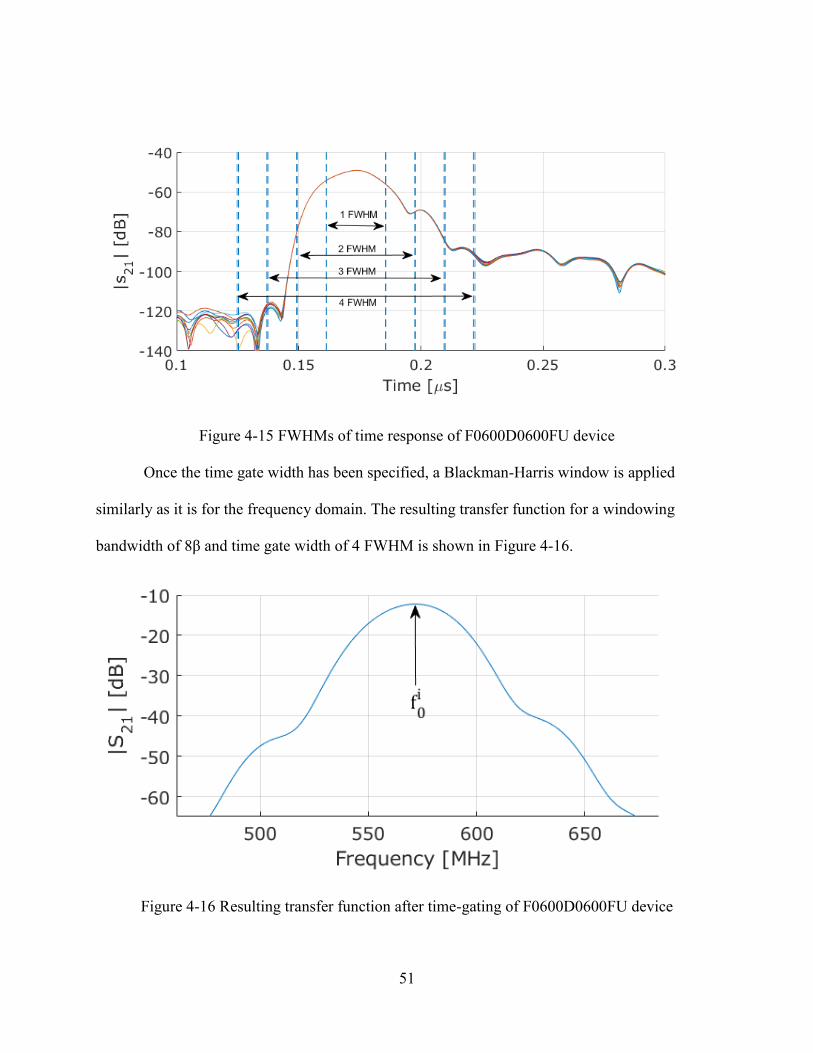
51
Figure 4-15 FWHMs of time response of F0600D0600FU device
Once the time gate width has been specified, a Blackman-Harris window is applied
similarly as it is for the frequency domain. The resulting transfer function for a windowing
bandwidth of 8β and time gate width of 4 FWHM is shown in Figure 4-16.
Figure 4-16 Resulting transfer function after time-gating of F0600D0600FU device

52
The side lobes shown in the S21 response are suppressed, which is a property of the
Blackman-Harris window function [57]. The center frequency 𝑓0𝑖 is determined by taking the
three-point maximum and applying Equation (4-4), just like determining the peak of the time
response. Since the group velocity is a result of a pair of delay lines, the center frequency for a
pair is obtained by averaging the center frequencies determined for each delay line individually,
where this quantity is denoted as simply 𝑓0. The typical distance between the center frequencies
of two delay lines in a pair is within a few MHz. When discussing a certain group velocity
resulting from a pair, the variable 𝑓0 is referenced. As mentioned, the width of the time gate and
frequency window bandwidth both have a direct influence on the center frequency
determination, which will be discussed in the next section.
4.1.3. Phase Velocity and Center Frequency Determination
Once the group velocity has been evaluated, the phase velocity can be found. Since the
SAW velocity problem is computationally more suited to phase velocity, it is advantageous to
determine the phase velocity of the delay lines. To accomplish this, one must first use an
estimate for the phase velocity. This estimate could be either the determine group velocity for a
free surface, or a polynomial that fits the resulting group velocities as a function of frequency for
the metallized surface. This polynomial can be expressed as phase velocity in terms of the
determined coefficients. The estimate is used to give a first guess for the phase velocity which is
then corrected using the phase response of the S21 measurement. This requires finding the point
of the phase difference between a pair of delay lines to be zero, causing the velocity to be an
integer number of wavelengths in the differential delay line path ∆𝑠. This frequency is the zero-
phase frequency 𝑓𝑚, and is selected as close as possible to the determined 𝑓0 of the pair where
the phase difference is zero. Finding the value of 𝑓𝑚 will be discussed shortly. Once the

53
approximate number of wavelengths in the differential length is determined, the actual number of
wavelengths is found by rounding to the nearest integer, which is used to recalculate the actual
value for the phase velocity. This procedure is shown in Figure 4-17.
Figure 4-17 Procedure for calculating phase velocity from group velocity
The phase velocity is found by finding the frequency where there is an integer number of
wavelengths existing within the differential delay length. The frequencies that meet these criteria
are the frequencies of which the phase difference between the two devices under question is zero,
implying that they are in-phase. This frequency will be known as the zero-phase frequency 𝑓𝑚.
The following derivation for estimating and correcting the phase velocity comes from [52]. For a
pair of delay lines, the effects of the IDTs can be canceled out by dividing the S21 responses after
time-gating.
𝑆21𝐼
𝑆21𝐼𝐼 =
𝑆21,𝐼𝐷𝑇𝑠𝐼
𝑆21,𝐼𝐷𝑇𝑠𝐼𝐼
𝑆21,𝑑𝑒𝑙𝑎𝑦𝐼
𝑆21,𝑑𝑒𝑙𝑎𝑦𝐼𝐼 = 𝑒−𝑗𝑘(𝐿1−𝐿2) = 𝑒−𝑗𝑘Δ𝑠𝑒𝑗2𝜋𝑚,
(4-7)
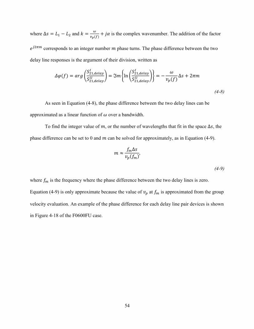
54
where Δ𝑠 = 𝐿1 − 𝐿2 and 𝑘 =𝜔
𝑣𝑝(𝑓)+ 𝑗𝛼 is the complex wavenumber. The addition of the factor
𝑒𝑗2𝜋𝑚 corresponds to an integer number 𝑚 phase turns. The phase difference between the two
delay line responses is the argument of their division, written as
𝛥𝜑(𝑓) = 𝑎𝑟𝑔 (𝑆21,𝑑𝑒𝑙𝑎𝑦
𝐼
𝑆21,𝑑𝑒𝑙𝑎𝑦𝐼𝐼 ) = ℑ𝔪{ln (
𝑆21,𝑑𝑒𝑙𝑎𝑦𝐼
𝑆21,𝑑𝑒𝑙𝑎𝑦𝐼𝐼 )} = −
𝜔
𝑣𝑝(𝑓)Δ𝑠 + 2𝜋𝑚
(4-8)
As seen in Equation (4-8), the phase difference between the two delay lines can be
approximated as a linear function of 𝜔 over a bandwidth.
To find the integer value of 𝑚, or the number of wavelengths that fit in the space Δ𝑠, the
phase difference can be set to 0 and 𝑚 can be solved for approximately, as in Equation (4-9).
𝑚 ≈𝑓𝑚Δ𝑠
𝑣𝑝(𝑓𝑚),
(4-9)
where 𝑓𝑚 is the frequency where the phase difference between the two delay lines is zero.
Equation (4-9) is only approximate because the value of 𝑣𝑝 at 𝑓𝑚 is approximated from the group
velocity evaluation. An example of the phase difference for each delay line pair devices is shown
in Figure 4-18 of the F0600FU case.

55
Figure 4-18 Phase difference between each pair of delay lines for F0600FU devices with the
zero-phase point indicated by the dashed line
The dash-dotted (-.) line indicates the determined 𝑓𝑚. It is noted that the phase response is
mostly distorted outside the frequency range of approximately 540 MHz to 600 MHz. Once the
approximate value for 𝑚 has been found, the number of wavelengths in Δ𝑠 is determined by
rounding 𝑚 to the nearest integer, which is used to find the true phase velocity.
𝑣𝑝(𝑓𝑚) =𝑓𝑚Δ𝑠
𝑚= 𝜆𝑓𝑚
(4-10)
Since locating the value of 𝑓𝑚 requires an estimate in 𝑓0 as the starting point, and as
mentioned before the center frequency has a dependence on the time-gating and frequency
window bandwidth, which is shown in Figure 4-19. As seen, there is a variation of a couple
MHz, however one phase turn occurs over about 10 MHz for the long delay line and 20 MHz for
the short delay lines, as shown in Figure 4-18. This means that the likelihood of falling into a
different phase turn is almost negligible, since 𝑓𝑚 varies less than 0.2 MHz, as shown in Figure

56
4-20. The variation in frequency over different windowing parameters appears to have a
variation within 0.2 MHz for all devices. This variation is directly coupled to the variation in
phase velocity, therefore the resulting measurement error of 0.02% for the phase velocity was
propagated to the final constant extraction procedure.
Figure 4-19 Center frequency f0 versus time gate width and windowing bandwidth
Figure 4-20 Zero-phase frequency fm versus time gate width and windowing bandwidth

57
There exists an ambiguity when determining the true wavelength, which can be resolved
by using multiple measured distances [58]. For the longest delay line pair, there are twice as
many phase turns in one period of the short delay line pairs since the slope of Equation (4-8) is
twice as large due to the doubling of Δ𝑠. This can assist in resolving the ambiguity by computing
the value of 𝑚 for each case. If the integer for the long delay pair is not double the short delay
pair, then that is the incorrect value for 𝑚 and therefore the incorrect 𝑓𝑚 since that would imply a
non-integer value for the short pair, which is not true. When this condition arises, the long delay
line is corrected to search in the phase turn where the 𝑓𝑚 matches that of the short delay line.
This case occurs if the center frequency 𝑓0 of a pair is close to a phase turn, as illustrated in
Figure 4-21. Each of the vertical dashed lines indicate the determined center frequencies 𝑓0 for
each pair in Figure 4-21a and the vertical dashed lines in indicates the resulting 𝑓𝑚 in Figure
4-21b. It can be seen that in the event of different 𝑓𝑚 values, different values for 𝑚 will occur.
The ambiguity in the zero-phase frequency is resolved by having two different differential delay
lengths. For example, the value of 𝑚 = 57 for the long delay line pair derives from an 𝑓𝑚 that is
not zero for the short delay pair, as that would imply a value of 𝑚 of 28.5. Therefore, the correct
value of m in this case is m = 58 for the long delay line, which corresponds to m = 29 for the
short delay line.

58
Figure 4-21 Phase difference showing possibility of two fm values
The free-surface phase velocity found using this correction technique are shown in Figure
4-22 and Figure 4-23 for the two orientations.
Figure 4-22 Measured phase velocities for free surface ψ = 0° orientation

59
Figure 4-23 Measured phase velocities for free surface ψ = 53° orientation
The red lines indicate a downward linear slope to the measured, which reflects the
dispersion. The free surface results in Figure 4-22 and Figure 4-23 shows dispersive behavior,
which is believed to be a product of surface roughness, as discussed in [59]. The extrapolated
zero-frequency phase velocity is compared with the free surface velocity used from simulation.
The results are summarized in Table 4-1.
Table 4-1 Results of measured free surface phase velocity
Orientation Simulation Measured [m/s] Deviation from
Simulation [ppm]
Dispersion
[ppm/GHz]
ψ = 0° 3978.78 3979.50 +181 -844
ψ = 53° 3571.21 3572.63 +398 -431
The comparison of the measured phase velocities to simulation show acceptable
agreement which validates the phase velocity extraction method and builds confidence for

60
metallized device phase velocity extraction. For the metallized case, the group velocity cannot be
normally used as a good estimate for the phase velocity due to the dispersion of a layered system.
Therefore, a method to calculate the phase velocity as a function of frequency from the group
velocity is required.
Each point of the metallized group velocity and corresponding frequency can be fitted to
a second-order polynomial. As frequency goes to zero, the group and the phase velocities tend to
the same value. If a polynomial fitting is done with the above 500 MHz measured data only, then
the discrepancy of value obtained as frequency goes to zero becomes unrealistic and
unacceptable. To obtain a realistic fitting, with reasonable polynomial coefficients, the data
points should be guided by inserting a reasonable value of phase velocity for the infinitesimally
thin perfect conductor metallic film case (frequency tending to zero). This reasonable value can
be obtained through the calculation of the infinitesimally thin metallic layer for each specific
substrate orientation. Since only a good estimate for the phase velocity is required, using a
simulated point is adequate for computing the initial phase velocity guesses required for finding
m. A second-order polynomial expression for the group velocity is written as
𝑣𝑔 = 𝑣0(1 + 𝑎1𝑓 + 𝑎2𝑓2),
(4-11)
where 𝑣0 is the simulated metallized velocity of the substrate and the coefficients 𝑎1 and 𝑎2 are
the result of fitting the group velocity results versus frequency. Using these parameters, an
expression for the phase velocity can be found using the definitions for group and phase velocity,
𝑣𝑔 =𝑑𝜔
𝑑𝑘= 2𝜋
𝑑𝑓
𝑑𝑘; 𝑣𝑝 =
𝜔
𝑘= 2𝜋
𝑓
𝑘.
(4-12)
By solving for 𝑘 and substituting Equation (4-11) for 1
𝑣𝑔 gives

61
𝑘 = 2𝜋 ∫1
𝑣𝑔𝑑𝑓 = 2𝜋
[ 2 tan−1 (
𝑎1 + 2𝑎2𝑓
√4𝑎2 − 𝑎12)
𝑣0√4𝑎2 − 𝑎12
+ 𝐶
]
= 2𝜋[𝑘0(𝑓) + 𝐶],
(4-13)
where 𝑘0(𝑓) =
2 tan−1(𝑎1+2𝑎2𝑓
√4𝑎2−𝑎12)
𝑣0√4𝑎2−𝑎12
. To find the value of the integration constant 𝐶, a boundary
condition as 𝑓 → 0 must be applied to give the SAW metallized velocity such that 𝑣𝑝(𝑓 → 0) =
𝑣0. The phase velocity can be written as a function of frequency with the 𝑘 expression:
𝑣𝑝(𝑓) =2𝜋𝑓
2𝜋(𝑘0(𝑓) + 𝐶)
(4-14)
and using the condition that lim𝑓→0
𝑣𝑝(𝑓) = 𝑣0 allows Equation (4-13) to be rewritten as
𝑣0(𝑘0(0) + 𝐶) = 0,
(4-15)
yielding
𝐶 = −
2 tan−1 (𝑎1
√4𝑎2 − 𝑎12)
𝑣0√4𝑎2 − 𝑎12
.
(4-16)
Therefore,
𝑣𝑝(𝑓) =𝑣0√4𝑎2 − 𝑎1
2𝑓
2 [tan−1 (𝑎1 + 2𝑎2𝑓
√4𝑎2 − 𝑎12) − tan−1 (
𝑎1
√4𝑎2 − 𝑎12)]
.
(4-17)

62
Equation (4-17) is the expression that is used to estimate the phase velocity to determine
the true phase velocity for the case of a metal layer. The measured group velocities and
associated second-order polynomials are plotted in Figure 4-24 and Figure 4-25.
Figure 4-24 Measured group velocities along with group and phase velocity polynomials for ψ =
0° orientation

63
Figure 4-25 Measured group velocities along with group and phase velocity polynomials for ψ =
53° orientation
It is noted that the effect of the disruptive guided mode appears in the form of larger
uncertainty in group velocity for the ψ = 53° orientation at the higher frequencies. However, the
error in the group velocities is compensated when converted to the polynomial expression, due to
the insensitivity of the rounded 𝑚 value with varying phase velocity estimations. All phase
velocity measurements for the metallized case were found to be within 0.03% of an average
value of all wafers for each device case. Their respective uncertainties for each case are
considered in the constant extraction procedure including the 0.02% measurement error from the
windowing bandwidth mentioned earlier.
4.2 Results of C11 vs. C44 Extraction
With the phase velocities obtained and the measured physical parameters of the film,
namely the film thickness and density, one can extract C11 and C44. Section 2.2.2 describes the
procedure for finding the solution for the isotropic constants given phase velocity, the thickness

64
and the density of the film. Once each individual C11 vs. C44 curve is generated for every
combination of velocity, height, and density uncertainties, the cross-over points can be computed
to obtain a set of C11 and C44 points. This result is shown for the 750 MHz device case in Figure
4-26.
The ψ = 0° rotation is the set of blue lines and the ψ = 53° rotation is the set of red lines.
The cluster of yellow points mark where each of the red and blue lines cross, represented by the
histogram in Figure 4-27. Due to the Gaussian behavior of the points, the determined values of
C11 and C44 can be expressed in terms of the mean and standard deviation of the point clusters.
Figure 4-26 C11 vs. C44 for 750 MHz device configuration with ψ = 0° as the blue lines and ψ =
53° as the red lines

65
Figure 4-27 Histogram of collected cross-over points for C11 and C44
For each device pitch, the values for C11 and C44 have been determined and are shown in
Figure 4-28 and Figure 4-29. The center points represent the average value of the collected
points from the Gaussian distribution and the error bars represent the standard deviation of the
mean.

66
Figure 4-28 C11 versus device frequency
Figure 4-29 C44 versus device frequency
As seen from Figure 4-28 and Figure 4-29, the thin-film isotropic elastic constant
responses with frequency show consistent trends from 650 to 850 MHz: C11 decreases linearly
and C44 is approximately constant. For the broader frequency range, the variations in C11 and C44
do not follow this linear pattern, as suggested for the transverse isotropic case shown in Figure
2-12 and Figure 2-13. This could have to do with the fact that the film may have some
polycrystalline alignment that detracts from an isotropic film assumption, but not exactly like the

67
transverse isotropic case, which has a polycrystalline hexagonal lattice with strong <111>
component facing up.
The percent standard deviation from the mean of the elastic constants found for each
device frequency is shown in Figure 4-30.
Figure 4-30 Uncertainty of elastic constants versus device frequency
As seen from Figure 4-30, the uncertainty for C44 is a few percent smaller than C11,
assuming values at around 2% deviation. The C11 deviation decreases with device frequency
increase, which is consistent with the decrease in sensitivity of the elastic constants to phase
velocity as frequency increases.
The data points calculated for C11 and C44 from all the frequency points were used to
compute a weighted average as employed like in Section 2.2.2, meaning the elastic constants
determined at the higher frequencies are given more weight. The results are shown in Table 4-2
for the two different height inputs from Table 3-2. The original Hill’s average constants for Cu is
shown here to compare with the constants found for the composite Cu film. The pure isotropic

68
Cu elastic constants are different from the determined film primarily due to the measured film
not being entirely Cu and believed to not be truly isotropic.
If the larger uncertainty in the thickness measurement is used, a larger density uncertainty
is also results, and thus the variance of the elastic constants will increase due to the larger
propagated error, as seen from Table 4-2.
When using only the profilometry measurements, the thickness changes to 2650.1 10.4
Å. With this uncertainty, the error propagates to the results of C11 and C44. This result can also be
observed in Figure 4-31 for a 750 MHz device, where a larger range of crossover points is seen,
as opposed to a smaller thickness uncertainty, which results in a smaller range of crossover
points.
Table 4-2 Determined elastic constants compared to accepted isotropic Cu constants
Elastic Constants Hill’s Average This work
Thickness
measurement
-
Profilometry + AFM
(weighted average)
Profilometry only
Thickness [Å] - 2649 3.64 2650.1 10.4
C11 [GPa] 200.87 226.5 3.5 228.1 7.4
C44 [GPa] 47.3 42.6 0.3 42.7 0.7

69
Figure 4-31 750 MHz device with larger thickness measurement uncertainty
The results for C11 and C44 are shown for the case of the profilometry thickness
measurement in Figure 4-32 and Figure 4-33.
Figure 4-32 C11 error bars for larger thickness uncertainty

70
Figure 4-33 C44 error bars for larger thickness uncertainty.
The percent error deviation for each device frequency is represented in Figure 4-34 and is
noticeably larger than with a smaller thickness uncertainty shown in Figure 4-30.
Figure 4-34 Percent error in elastic constants for larger thickness uncertainty.
The determined constants reported in Table 4-2 were put back into the simulation to
check for self-consistency between the SAW velocity simulation and the measured velocities.

71
The simulation over the measurement points is shown in Figure 4-35 and Figure 4-36 to illustrate
self-consistency.
Figure 4-35 Simulation vs. measurement for both orientations using determined constants using
the thickness 2649 3.64 Å
Figure 4-36 Simulation vs. measurement for both orientations using determined constants using
the thickness 2650.1 10.4 Å

72
The measured phase velocities for both orientations appear within the uncertainty range
reported in Table 4-2 and are self-consistent using the external thickness and density
measurements. The thickness uncertainty that was propagated through the simulation came from
the weighted average of both profilometry and AFM measurements from Table 3-3.

73
CHAPTER 5
CONCLUSION
5.1. Summary
The elastic constants C11 and C44 of an assumed isotropic Cu-based multilayer film were
extracted using several SAW differential delay lines designed over the frequency range of
approximately 500 MHz to 900 MHz. Two different crystal orientations on the same crystal cut
of a LiNbO3 substrate were used for the constant determination.
The thickness of the film under investigation was determined using profilometry and
AFM measurements, and the density of the film was found by weighing the wafer before and
after deposition and using the thickness measurements and the area of the wafer. The RF
responses of the delay lines were measured, and the processed data was used to find the time
delay for the group velocity determination and the center frequencies. To find the phase velocity,
the measured phase response of S21 was used to correct a polynomial estimation of the phase
velocity given by the group velocity and center frequency results.
The measured thickness, density, and center frequencies were used to simulate a
dataspace of possible phase velocities spanning over reasonable ranges of various values of C11
and C44. The determined phase velocities were used to interpolate C11 and C44 values that exist
on the computed dataspace. The measurement uncertainties for all values were included to
propagate the error to the final determined elastic constant values. The C11 and C44 results show
self-consistency over the frequency range of interest and verified to be heavily dependent on the
actual height and density of the film parameter inputs.

74
5.2. Contributions
This thesis provides a summary on the methods used for thin film characterization for
SAW and investigates a technique to evaluate the isotropic elastic properties of a thin metal film.
The stiffness of the Cu-based film was extracted on one crystal cut of an orientation near 128°-Y
cut LiNbO3 using two wafer orientations. A study on the sensitivity of the SAW phase velocity
to varying film parameters was performed to evaluate the effectiveness of using the rotated
orientation and a method to generate a data space using Adler’s matrix method SAW calculation
routine. The possible transverse isotropy of the thin film was observed and considered to be of
no object when modelling the multilayer film as a single isotropic film.
Using statistical analysis of the propagated measured input value uncertainties in
thickness, density, and phase velocity measurement, the error in the determined elastic constants
was found to be within 3.2% for the cases shown over the desired frequency range. This shows
that the techniques developed is appropriate for the quick extraction of isotropic elastic
constants, which is extremely important in the design and simulation of modern SAW resonators
and other SAW structures.
5.3. Future Work
The results have yet to be scrutinized and tested for confirmation on other devices. One
method of confirming the accuracy could be simulating resonators using the determined
constants and see how well they fit to resonators and/or other SAW devices that were fabricated
on the same wafers. The resonator response frequency would be simulated using both the elastic
constants that were computed and the isotropic Hill average for pure Cu for comparison.
Another way to confirm the obtained elastic constants could be to use the guided mode
on ψ = 53° or another PSAW orientation for data comparison instead of only the Rayleigh mode.

75
Due to the inconclusive results given from the mixed-mode responses on the ψ = 53° orientation,
the usage of the PSAW along this orientation may pose some challenges.
Although the film in this work was successfully modelled as a single isotropic film for
elastic constant extraction, the tendency of Cu films growing with a potentially transverse
isotropic structure gives rise to additional possible investigation of characterizing polycrystalline
films that would not accurately fit the isotropic model of the stiffness characterization.
Another interesting characterization of the film not covered in this work, and therefore
suggested as future work, refers to the measurement and characterization of the losses in the film
as a function of frequency.
Finally, the technique showed to be robust enough to grant its use for the extraction of
elastic constants of dielectric thin films, currently used for temperature compensation in
contemporary RF SAW components. The electrical permittivity of a dielectric film must be
measured and taken into consideration as a film parameter, similarly to the measured thickness
and density values.

76
REFERENCES
[1] D. P. Morgan, “A HISTORY OF SURFACE ACOUSTIC WAVE DEVICES,” Int. J.
High Speed Electron. Syst., vol. 10, no. 03, pp. 553–602, Sep. 2000.
[2] A. J. Slobodnik, T. L. Szabo, and K. R. Laker, “Miniature Surface-Acoustic-Wave
Filters,” vol. 67, no. 1, 1979.
[3] T. Bauer and C. Eggs, “A Bright Outlook for Acoustic Filtering,” IEEE Microw. Mag., no.
August, pp. 73–81, 2015.
[4] H. Nakanishi, H. Nakamura, Y. Hamaoka, H. Kamiguchi, and Y. Iwasaki, “Small-Sized
saw duplexers with wide duplex gap on a Sicval/Linbos structure by using Novel
Rayleigh-mode spurious suppression technique,” Proc. - IEEE Ultrason. Symp., pp. 1588–
1591, 2008.
[5] R. Ruby, P. Bradley, J. D. Larson, and Y. Oshmyansky, “PCS 1900 MHz duplexer using
thin film bulk acoustic resonators (FBARs),” Electron. Lett., vol. 35, no. 10, p. 794, 1999.
[6] R. Aigner, “SAW and BAW technologies for RF filter applications: A review of the
relative strengths and weaknesses,” 2008 IEEE Ultrason. Symp., pp. 582–589, 2008.
[7] S. Mahon, R. Aigner, T. Semiconductor, B. St, and B. C. Bend, “Bulk Acoustic Wave
Devices – – Why , How , and Where They are Going ( Film Bulk Acoustic Resonator ),”
Most, pp. 15–18, 2007.
[8] D. F. Mccann et al., “A Lateral-Field-Excited LiTaO3 High-Frequency Bulk Acoustic
Wave Sensor,” IEEE Trans. Ultrason. Ferroelectr. Freq. Control, vol. 56, no. 4, pp. 779–
787, 2009.
[9] E. A. Gerber, T. Lukaszek, and A. Ballato, “Advances in Microwave Acoustic Frequency
Sources,” IEEE Trans. Microw. Theory Tech., vol. MTT-34, no. 10, pp. 1002–1016, 1986.
[10] A. Ballato, E. R. Hatch, and T. Lukaszek, “Lateral-field coupling,” pp. 339–342, 1986.
[11] A. Maskay and M. Pereira Da Cunha, “High temperature static strain microwave acoustic
sensor,” IEEE Int. Ultrason. Symp. IUS, vol. 2016–Novem, 2016.
[12] R. S. Falconer, “A Theoretical and Experimental Study of a Conductivity - Surface
Acoustic Wave Gas Microsensor.,” UNIVERSITY OF MAINE, 1993.
[13] J. Pouliquen and G. Vaesken, “Effect of a metallic thin film on the propagation of
Rayleigh waves,” J. Appl. Phys., vol. 44, no. 4, pp. 1524–1526, 1973.
[14] K. Hashimoto, “Simulation of Surface Acoustic Wave Devices,” Jpn. J. Appl. Phys., vol.
45, no. 5B, pp. 4423–4428, 2006.
[15] C. V. Thompson and R. Carel, “Texture development in polycrystalline thin films,”
Mater. Sci. Eng. B, vol. 32, no. 3, pp. 211–219, 1995.
[16] W. M. Kuschke, A. Kretschmann, R. M. Keller, R. P. Vinci, C. Kaufmann, and E. Arzt,
“Textures of thin copper films,” J. Mater. Res., vol. 13, no. 10, pp. 2962–2968, 1998.

77
[17] A. J. Slobodnik, “A Review of Material Tradeoffs in the Design of Acoustic Surface
Wave Devices at VHF and Microwave Frequencies,” IEEE Trans. Sonics Ultrason., vol.
20, no. 4, pp. 315–322, 1973.
[18] H. Schmidt, R. Kunze, M. Weihnacht, and S. B. Menzel, “Investigation of
acoustomigration effects in Al-based metallizations,” 2002 IEEE Ultrason. Symp.
Proceedings, Vols 1 2, vol. 00, no. c, pp. 415–418, 2002.
[19] S. Menzel, M. Pekarčikova, M. Hofmann, T. Gemming, and K. Wetzig, “Material
transport in Al-metallizations of power-loaded SAW structures,” Appl. Surf. Sci., vol. 252,
no. 1 SPEC. ISS., pp. 215–217, 2005.
[20] T. Omori and S. Nakagomi, “SAW reflection characteristics of Cu electrodes and their
application to SAW IF devices,” Ultrason. …, vol. 00, no. c, pp. 19–23, 2002.
[21] M. Spindler, S. B. Menzel, C. Eggs, J. Thomas, T. Gemming, and J. Eckert, “TEM
investigation of Ti and Ti/Al bilayer as alternative diffusion barriers for Cu metallization
for SAW device applications,” Microelectron. Eng., vol. 85, no. 10, pp. 2055–2058, 2008.
[22] C. Zhou et al., “Temperature-Compensated High-Frequency Surface Acoustic Wave
Device,” IEEE Electron Device Lett., vol. 34, no. 12, pp. 1572–1574, 2013.
[23] K. Hashimoto et al., “Recent Development of Temperature Compensated SAW Devices,”
pp. 79–86, 2011.
[24] M. Tomar, V. Gupta, K. Sreenivas, and A. Mansingh, “Temperature stability of ZnO thin
film SAW device on fused quartz,” IEEE Trans. Device Mater. Reliab., vol. 5, no. 3, pp.
494–500, 2005.
[25] Y. Wang et al., “A zero TCF band 13 SAW duplexer,” 2015 IEEE Int. Ultrason. Symp.
IUS 2015, pp. 13–16, 2015.
[26] F. S. HICKERNELL, “THIN-FILMS FOR SAW DEVICES,” Int. J. High Speed Electron.
Syst., vol. 10, no. 03, pp. 603–652, Sep. 2000.
[27] A. Neubrand and P. Hess, “Laser generation and detection of surface acoustic waves:
Elastic properties of surface layers,” J. Appl. Phys., vol. 71, no. 1, pp. 227–238, 1992.
[28] M. G., “Acoustic Waves: A Probe for the Elastic Properties of Films,” in Acoustic Waves -
From Microdevices to Helioseismology, vol. 56, no. C, InTech, 2011, pp. 604–609.
[29] G. M. Pharr and W. C. Oliver, “Measurement of thin film mechanical properties using
nanoindentation,” Mrs Bull., vol. 17, no. 7, pp. 28–33, 1992.
[30] V. I. Anisimkin, I. M. Kotelyanskii, P. Verardi, and E. Verona, “Elastic properties of thin-
film palladium for surface acoustic wave (SAW) sensors,” Sensors Actuators B. Chem.,
vol. 23, no. 2–3, pp. 203–208, 1995.
[31] B. A. Auld, Acoustic fields and waves in solids. Рипол Классик, 1973.
[32] E. L. Adler, “Matrix methods applied to acoustic waves in multilayers.,” IEEE Trans.
Ultrason. Ferroelectr. Freq. Control, vol. 37, no. 6, pp. 485–490, 1990.

78
[33] G. Grunauer et al., “Derivation of accurate tensor data of materials in SAW devices by
solving a parameter identification problem using an enhanced eigenvalue analysis of an
infinite array model,” IEEE Int. Ultrason. Symp. IUS, no. 4, pp. 1700–1703, 2013.
[34] E. C. Jelks and R. S. Wagers, “Elastic constants of electron-beam-deposited thin films of
molybdenum and aluminum on LiNbO3,” in Ultrasonics Symposium, 1983, pp. 319–322.
[35] W. Ruile and H. Meier, “Films for Improved Cad Modeling of Saw Filters and
Resonators,” in Ultrasonics Symposium, 1992, pp. 437–440.
[36] S. Makarov, E. Chilla, and H. J. Fröhlich, “Determination of elastic constants of thin films
from phase velocity dispersion of different surface acoustic wave modes,” J. Appl. Phys.,
vol. 78, no. 8, pp. 5028–5034, 1995.
[37] D. Gallimore, T. Moonlight, and M. Pereira, “Extraction of Pt / Rh / ZrO 2 High
Temperature Elastic Constants,” in Ultrasonics Symposium (IUS), 2009 IEEE
International, 2009, pp. 2797–2800.
[38] M. Knapp et al., “Accurate characterization of SiO2 thin films using surface acoustic
waves,” IEEE Trans. Ultrason. Ferroelectr. Freq. Control, vol. 62, no. 4, pp. 736–743,
2015.
[39] G. Kovacs, M. Anhorn, H. E. Engan, G. Visintini, and C. C. W. Ruppel, “Improved
material constants for LiNbO3 and LiTaO3,” IEEE Symp. Ultrason., pp. 435–438, 1990.
[40] A. H. Fahmy and E. L. Adler, “Propagation of acoustic surface waves in multilayers: A
matrix description,” Appl. Phys. Lett., vol. 22, no. 10, pp. 495–497, 1973.
[41] A. H. Fahmy and E. L. Adler, “Transformation of tensor constants of anisotropic materials
due to rotations of the co-ordinate axes,” Proc. IEEE, vol. 122, no. 5, pp. 591–592, 1975.
[42] E. L. Adler, “BULK AND SURFACE ACOUSTIC WAVES IN ANISOTROPIC
SOLIDS,” Int. J. High Speed Electron. Syst., vol. 10, no. 03, pp. 653–684, Sep. 2000.
[43] R. Hill, “The Elastic Behaviour of a Crystalline Aggregate,” Proc. Phys. Soc. Sect. A, vol.
65, no. 5, pp. 349–354, 1952.
[44] H. M. Ledbetter and E. R. Naimon, “Elastic Properties of Metals and Alloys. II. Copper,”
J. Phys. Chem, vol. 3, no. 4. pp. 897–935, 1974.
[45] O. L. Anderson, “Determination and Some Uses of Isotropic Elastic Constants of
Polycrystalline Aggregates Using Single-Crystal Data,” Phys. Acoust., vol. 3, pp. 43–95,
1965.
[46] J. Taylor, Introduction to error analysis, the study of uncertainties in physical
measurements, 2nd ed. 1997.
[47] D. B. Knorr and D. P. Tracy, “A review of microstructure in vapor deposited copper thin
films,” Mater. Chem. Phys., vol. 41, no. 3, pp. 206–216, 1995.
[48] D. P. Tracy, D. B. Knorr, and K. P. Rodbell, “Texture in multilayer metallization
structures,” J. Appl. Phys., vol. 76, no. 5, pp. 2671–2680, 1994.

79
[49] N. Nakamura et al., “Study of elastic anisotropy of Cu thin films by resonant-ultrasound
spectroscopy coupled with laser-doppler interferometry and pump-probe photoacoustics,”
Japanese J. Appl. Physics, Part 1 Regul. Pap. Short Notes Rev. Pap., vol. 45, no. 5 B, pp.
4580–4584, 2006.
[50] B. C. Hendrix and L. G. Yu, “Self-consistent elastic properties for transversely isotropic
polycrystals,” Acta Mater., vol. 46, no. 1, pp. 127–135, 1998.
[51] R. Thomas, T. W. Johannes, W. Rude, and R. Weigel, “Determination of Phase Velocity
and Attenuation of Surface Acoustic Waves With Improved Accuracy,” in Ultrasonics
Symposium, 1998, pp. 277–282.
[52] M. Knapp, “Charakterisierung funktionaler Schichten für Oberflächenwellenfilter.” Prof.
Dr. Leonhard M. Reindl, Freiburg, 2015.
[53] M. S. Blois and L. M. Rieser, “Apparent density of thin evaporated films,” J. Appl. Phys.,
vol. 25, no. 3, pp. 338–340, 1954.
[54] C. S. Hartmann, D. T. Bell, and R. C. Rosenfeld, “Impulse Model Design of Acoustic
Surface-Wave Filters,” IEEE Trans. Microw. Theory Tech., vol. MTT-21, no. 4, pp. 162–
175, 1973.
[55] J. H. Kuypers, L. M. Reindl, S. Tanaka, and M. Esashi, “Maximum accuracy evaluation
scheme for wireless SAW delay-line sensors,” IEEE Trans. Ultrason. Ferroelectr. Freq.
Control, vol. 55, no. 7, pp. 1640–1652, 2008.
[56] I. Shrena, D. Eisele, L. Reind, and J. Bardong, “High precision signal processing
algorithm to evaluate the SAW properties as a function of temperature,” Ultrason. Symp.
(IUS), 2009 IEEE Int., vol. 60, no. 4, pp. 805–813, 2009.
[57] F. J. Harris, “On the use of windows for harmonic analysis with the discrete Fourier
transform,” Proc. IEEE, vol. 66, no. 1, pp. 51–83, 1978.
[58] D. Schneider, T. Schwarz, and B. Schultrich, “Determination of elastic modulus and
thickness of surface layers by ultrasonic surface waves,” Thin Solid Films, vol. 219, no. 1–
2, pp. 92–102, 1992.
[59] R. C. Williamson, “Problems encountered in high-frequency surface-wave devices,” in
Ultrasonics Symposium, 1974.

80
APPENDIX: SAW PROPAGATION THEORY AND MATRIX METHOD
The fundamentals of SAW propagation is based upon elastic wave theory on a
piezoelectric substrate is outlined in this section according to Auld [31] and Adler [42]. The
development of the matrix methods used to compute SAW velocity and its implementation to
characterize films will follow.
A bulk acoustic wave is recognized as a combination of a compressional wave in the
propagation direction and two shear wave components, however the special case of acoustic
waves guided at the surface are of interest, known as Rayleigh waves. A Rayleigh wave can be
described by the stress and strain fields of a material at its surface by applying the proper
boundary conditions of an air-solid interface, where different partial wave modes contribute to
the overall behavior of a wave that is guided at the surface. The particles at the surface exhibit
elliptical oscillations whose amplitudes are strongest at the surface, but decay exponentially with
substrate depth.
Acoustic waves, also known as sound waves, correspond to a time-varying displacement
of particles in a medium caused by a varying stress field. The state of all stress fields at a point in
a solid can be represented by the Cauchy stress tensor for three dimensions as
[
𝑻𝑥
𝑻𝒚
𝑻𝑧
] = [
𝑇𝑥𝑥 𝑇𝑥𝑦 𝑇𝑥𝑧
𝑇𝑦𝑥 𝑇𝑦𝑦 𝑇𝑦𝑧
𝑇𝑧𝑥 𝑇𝑧𝑦 𝑇𝑧𝑧
] [�̂��̂��̂�
] ,
(A-1)
where 𝑻 is the Cauchy stress tensor with units 𝑁/𝑚2, and each component for the stress tensor
𝑇𝑖𝑗 corresponds to the i-directed traction force on the j-oriented face. For example, the 𝑇𝑧𝑦 term
denotes the traction force in the z-direction on a face perpendicular to the y-axis. Since we
assume no additional torque is acting on the solid, it is said that 𝑇𝑖𝑗 = 𝑇𝑗𝑖, else the solid would

81
rotate due to an imbalance in stresses. This allows for a reduction in size of the stress tensor due
to symmetry according to Voigt’s notation presented in Table A-1.
Table A-1 Adopted Voigt notation
Subscript: xx yy zz yz, zy xz, zx xy, yx
Voigt: 1 2 3 4 5 6
Voigt’s notation allows reduction of Equation (A-1) to the 6x1 stress tensor in Equation
(A-2) by substitution of the appropriate index and noting the assumed symmetry. Equation (A-2)
will be the basis for all subsequent formulations due to simplifications in the constitutive
equations.
𝑻 = [𝑇1 𝑇2 𝑇3 𝑇4 𝑇5 𝑇6]𝑡,
(A-2)
where the superscript t indicates matrix transpose. For an acoustic wave to propagate, the
pressure in the material must change with position, which introduces a deformation on the
particles in the body. These deformations can be represented by the particle displacements of a
medium by
𝒖 = [𝑢1 𝑢2 𝑢3]𝑡,
(A-3)
where 𝒖 is the particle displacement vector in units of meters, and each component indicates the
displacement of a particle from its equilibrium x, y, and z positions, respectively. The stress and
particle displacement fields are the primary quantities that represent a travelling sound wave in a
solid medium. These fields are related through Newton’s translational law of motion in Equation
(A-4), which describes the equilibrium of forces in a solid due to elastic displacements written as

82
∂𝑇𝑖𝑗
∂x𝑖= 𝜌
𝜕2𝑢𝑗
𝜕𝑡2, 𝑖, 𝑗 = 1,2,3,
(A-4)
where 𝜌 is the density of the material with units of 𝑘𝑔/𝑚3, and the labels x1, x2, and x3
correspond to the x, y, and z directions respectively. Here, 𝑇𝑖𝑗 represents the ith row and jth
column of the tensor, which can then be reduced using Voigt’s notation to obtain the stress field
described by Equation (A-2). The Voigt’s notation follows through the entire analyses, where the
subscripts 1, 2, and 3 are used interchangeably with the x, y, and z directional components.
Since the exact translational displacement of the particles is not relevant for SAW
velocity calculation, they may be represented as relative displacements, or strain. The strain
tensor is defined as the reduced 6 x 1 tensor, analogous to the modified stress tensor. The
relationship to the particle displacements is shown in Equation (A-5),
𝑺 = ∇𝑠𝒖,
(A-5)
where ∇𝑠 is the modified divergence operator matrix
∇𝑠=
[ 𝜕
𝜕𝑥0 0
0𝜕
𝜕𝑦0
0 0𝜕
𝜕𝑧
0𝜕
𝜕𝑦
𝜕
𝜕𝑧𝜕
𝜕𝑥0
𝜕
𝜕𝑧𝜕
𝜕𝑥
𝜕
𝜕𝑦0
]
,
(A-6)
reducing the strain field of Equation (A-5) to the tensor notation
83
𝑆𝑘𝑙 =1
2(𝜕𝑢𝑘
𝜕𝑥𝑙+
𝜕𝑢𝑙
𝜕𝑥𝑘) , 𝑘, 𝑙 = 1,2,3.
(A-7)
The strain tensor is a description of relative particle displacements, and therefore has no
units. The stress 𝑻 and strain 𝑺 are fundamentally related through Hooke’s law
𝑻 = 𝑪𝑺,
(A-8)
where 𝑪 is the 6 x 6 elastic stiffness tensor of units 𝑁/𝑚2, which is characteristic of the
material’s elasticity. The larger the elastic constant, the stiffer the material is. It is appropriate to
note that the 𝑪 in Equation (A-8) is reduced from a 9 x 9 matrix associated with the full 3 x 3
stress tensor from Equation (A-1) by symmetry and Voigt’s notation.
For an acoustic wave which travels in a solid that is non-piezoelectric, the theory
presented in the previous section can describe the continuum behavior of a sound wave, such as a
BAW. For application of acoustic waves to microwave engineering, the wave propagation in a
piezoelectric medium must be considered. The piezoelectric effect is fundamentally a
relationship between the mechanical and electrical displacements, where the electric field
induces a stress field and the mechanical strain induces an electric field. In electromagnetics, the
relationship between electric field 𝑬 and electric displacement 𝑫 is defined as
𝑫 = 휀𝑬
(A-9)
where 휀 is the 3 x 3 electrical permittivity matrix, and 𝑫 and 𝑬 are both 3 x 1 vectors. For a
medium that exhibits piezoelectricity, the Equations (A-8) and (A-9) can be coupled by
incorporating the 3 x 6 piezoelectric constant tensor 𝒆 to form the governing equations for a

84
piezoelectric material. The resulting stress and electric displacement fields are expressed in
tensor notation in Equations (A-10) and (A-11), respectively.
𝑇𝑖𝑗 = 𝑐𝐸𝑖𝑗𝑘𝑙𝑆𝑘𝑙 + 𝑒𝑘𝑖𝑗𝐸𝑘
(A-10)
𝐷𝑖 = 𝑒𝑗𝑘𝑙𝑆𝑘𝑙 + 휀𝑆𝑖𝑘𝐸𝑘
(A-11)
The superscripts E and S translate to the material constant measured at constant electric
field and constant strain, respectively. Voigt’s notation also reduces the four subscripts to only
two by corresponding the first and second subscript pairs to their Voigt number in Table A-1.
These relations make up the constitutive equations for a wave in a piezoelectric medium. Each
tensor relating to the material constants must be rotated in correspondence to the Euler angles,
described in a later section.
To simplify the analysis further, another important assumption is the quasi-static
approximation, which ignores the effects of electromagnetic wave propagation due to the
velocity of light being much greater than the velocity of a sound wave. The quasi-electrostatic
(or simply quasi-static) approximation assumes no time-varying magnetic field, which reduces
Faraday’s law to
∇ × 𝑬 = −𝜕𝑩
𝜕𝑡= 0,
(A-12)
where 𝑬 is the electric field vector and 𝑩 is the magnetic field. Since a vector field is irrotational
its curl is equal to zero, the electric field can be expressed electrostatically as the gradient of the
scalar potential,

85
𝑬 = −∇𝜑,
(A-13)
where 𝜑 is the electric potential. Using the definition of electric displacement from Equation
(A-9) in Equation (A-13) and taking the gradient will equate to LaPlace’s equation, ∇2𝜑 = 0,
resulting in
∇ ∙ 𝑫 = 0.
(A-14)
The assumed plane wave solutions to the wave equation can be written in terms of 𝒖 and
𝜑 as functions of time and space,
𝑢𝑗 = 𝛼𝑗𝑒𝑖𝜔𝑡𝑒−𝑖𝑘𝑥+𝛽𝑧, 𝑗 = 1,2,3,
(A-15)
𝜑 = 𝛼4𝑒𝑖𝜔𝑡𝑒−𝑖𝑘𝑥+𝛽𝑧,
(A-16)
where 𝑘 is the wave vector in the propagation x-direction, and 𝛽 is the attenuation in the positive
z-direction into the substrate. The 𝛼 terms denote the arbitrary amplitude of the elastic
displacements or electric potential. Note that there is no wave travelling in the z-direction, but
that the amplitude of the wave decays with depth into the substrate. It is characteristic of SAWs
for the field amplitudes to change with depth according to attenuation 𝛽, but solving for this
parameter is outside of the scope of this work, so the amplitudes will be represented simply as a
function of z. It is appropriate now to adopt the phasor notation for convenience. It can be seen
by differentiating Equations (A-15) and (A-16) that
𝜕
𝜕𝑡= 𝑗𝜔
(A-17)

86
and
𝜕
𝜕𝑥= −𝑗𝑘 = −𝑗
𝜔
𝑣𝑝
(A-18)
For the SAW problem, it assumed to propagate in the x-direction with decaying
amplitude in the z-direction, where the surface exists at 𝑧 = 0. The SAW is theorized to
propagate only in the sagittal plane, or x-z plane, thus, the following derivatives are assumed
𝜕
𝜕𝑥≠ 0,
𝜕
𝜕𝑧≠ 0,
𝜕
𝜕𝑦= 0
(A-19)
With these assumptions, Eric Adler’s matrix method [42] for calculating SAW velocities
may be described. The matrix method is derived from the piezoelectric constitutive equations
(A-10) and (A-11) by substituting the assumed solutions from (A-15) and (A-16) after using the
gradient operator on both equations. The field quantities can be solved for in terms of the
unknown derivative in the z-direction to form a wave equation. The ordinary differential
equation that results for the matrix method is shown in Equation (A-20),
𝜕𝝉
𝜕𝑧= 𝑗𝜔𝑨𝝉,
(A-20)
where the stress, electric, particle, and electric potential fields are represented by the 8 x 1 vector
𝝉 = [𝑻𝒛 𝐷𝑧 𝝂 𝑗𝜔𝜑]𝑡,
(A-21)
and can be alternatively written as

87
𝝉 = [𝝉𝑛
𝝉𝑣] , 𝝉𝑛 = [𝑻𝒛 𝐷𝑧]
𝒕, 𝝉𝑣 = [𝝂 𝑗𝜔𝜑]𝒕,
(A-22)
where
𝑻𝒛 = [𝑇31 𝑇32 𝑇33]𝑡 = [𝑇5 𝑇4 𝑇3]
𝑡 .
(A-23)
𝑻𝒛 represents the stresses on the substrate surface (z-plane) only, and 𝒗 is the 3 x 1
particle velocity vector, which is the time derivative of the particle displacements and can be
written in the phasor notation as in Equation (A-24).
𝝂 = [𝜕𝑢1
𝜕𝑡
𝜕𝑢2
𝜕𝑡
𝜕𝑢3
𝜕𝑡]𝑡
= 𝑗𝜔𝒖
(A-24)
The link between the surface stresses, particle motion and time dependence of the fields
in the ordinary differential equation from (A-20) comes from the material-dependent 8 x 8 𝑨
matrix defined as
𝑨 =
[ 𝜞13𝑿
𝑣𝑝𝑮 −
𝜞11 − 𝜞13𝑿𝜞31
𝑣𝑝2
𝑿𝑿𝜞31
𝑣𝑝 ]
,
(A-25)
where the 𝜞 matrices can be written for a specified 𝑖𝑘 index as
𝜞𝑖𝑘 = [
𝐶1𝑖1𝑘 𝐶1𝑖2𝑘 𝐶1𝑖3𝑘 𝑒𝑘1𝑖
𝐶1𝑖2𝑘 𝐶2𝑖2𝑘 𝐶2𝑖3𝑘 𝑒𝑘2𝑖
𝐶1𝑖3𝑘 𝐶3𝑖2𝑘 𝐶3𝑖3𝑘 𝑒𝑘3𝑖
𝑒𝑖1𝑘 𝑒𝑖2𝑘 𝑒𝑖3𝑘 −휀𝑖𝑘
] .
(A-26)
Additionally,

88
𝑿 = (𝚪33)−𝟏,
(A-27)
and the density matrix is
𝑮 = [
𝜌 0 0 00 𝜌 0 00 0 𝜌 00 0 0 0
] .
(A-28)
The 𝑨 matrix in Equation (A-25) not only depends on the substrate constants, but the
phase velocity as well, thus it is transcendental. Therefore, it is required to first assume a solution
to the ordinary differential Equation (A-20) and determine the correct phase velocity solution by
subjecting the system to boundary conditions and iterative calculations are required to minimize
the determinant of the boundary condition function. The solution to the system of ordinary
differential equations in (A-20) is assumed as
𝝉(𝑧) = exp(𝑗𝜔𝑨𝑧) 𝝉(0),
(A-29)
where 𝝉(0) is the vector of SAW field quantities at the substrate’s surface (i.e. z = 0). The
exponential matrix exp(𝑗𝜔𝑨𝑧) can be rewritten in terms of the eigenvectors 𝑼 and the diagonal
eigenvalue matrix 𝚲 of 𝑨 as
𝝉(𝑧) = 𝑼exp(𝚲z)𝑼−1𝝉(0)
(A-30)
where the exponential matrix has the form

89
exp(𝚲z) = [
𝑒𝜆1𝑧 0 ⋯ 00 𝑒𝜆2𝑧 ⋯ 0⋮ ⋮ ⋱ 00 0 0 𝑒𝜆𝑛𝑧
] ,
(A-31)
and 𝜆𝑛 is the 𝑛th complex eigenvalue of the form ±𝑎 ± 𝑗𝑏. The uncoupled state vector and is
defined as
�̅� = 𝑼−1𝝉.
(A-32)
Equation (A-32) is also known as the normal-mode weighting vector, and once it is found
can describe the SAW fields at any point z into the substrate by Equation (A-30). Once the
uncoupled state vector is known, the fields 𝝉 can be found at any point of the substrate depth z.
There are two cases of boundary conditions that occur in the calculation, free surface and
metallized surface, where both assume a stress-free surface and continuous particle
displacements. The free surface boundary condition additionally includes the continuous
behavior of the electric displacement at the surface interface with air. The metallized surface
assumes the substrate is covered with an infinitesimally thin perfectly conducting layer, which
shorts the electric potential between the surface and air. By solving the system under each of the
two boundary conditions, one will obtain the velocity of a SAW on the free surface and the
velocity under the metallized surface as described.
The first boundary condition applies for both free and metallized case, which is that the
surface is considered stress free as in Equation (A-33).
𝑻𝑧|𝑧=0 = 0
(A-33)

90
The free surface case requires that the normal component of the electric displacement
must be continuous at the surface, that is, the charge density between the substrate and air at the
interface is zero. Hence, the electric potential at the surface is continuous according to LaPlace’s
equation, which describes the potential in air. The normal electric displacement can be written in
terms of the electric potential by assuming continuous charge and applying the electrostatic
relationship 𝐷𝑧 = −휀0𝜕𝜑
𝜕𝑧, which reduces to
𝐷𝑧(0+) = 𝐷𝑧(0
−) = 휀0
𝜔
𝑣𝑝𝜑(0).
(A-34)
For the metallized circuit, the electric potential is zero by the short-circuit, hence the
boundary condition
𝜑(0) = 0.
(A-35)
Equations (A-34) and (A-35) are two separate boundary conditions used for solving two
different phase velocities, and Equation (A-33) is applied to both cases. Both the free and
metallized phase velocities are important in the evaluation of SAW properties of a substrate and
are solved for separately, which means that the calculation procedure involving the velocity
search must be performed twice, one for the free surface case and one for the metallized surface.
The 𝑨 matrix is the heart of the calculation therefore its proper evaluation is necessary
starting from rotating the constants to constructing and minimizing the boundary condition
function.
No matter what type of velocity search (i.e. free or metallized) is being performed, the
computations required are the same. The eigenvalues and eigenvectors must be sorted
accordingly by selecting the associated decaying partial modes (DPMs) of the piezoelectric half-

91
space. The corresponding eigenvectors to the DPMs are then used to construct the boundary
condition function (BCF) that follow either the short-circuited (metallized) or open-circuited
(free) cases. For an anisotropic substrate with finite electromechanical coupling, the free and
metallized velocities should be different. From the free and metallized velocities, the
electromechanical coupling coefficient can be determined.
The phase velocity is identified as the value which gives the minimum determinant of the
BCF, which is then used when solving for the SAW fields required to compute the power flow in
each direction, therefore the power flow angle. The basic calculation procedure of the SAW
velocity can be expanded upon by varying specific parameters and observing the change in
velocity to perform a sensitivity analysis.
Construction of the 𝑨 matrix begins with creation of the 𝜞 matrices and density matrix.
When building the 𝑨 matrix, there are three considerations that must be approached with care to
ensure proper calculation.
The 𝑨 matrix is generated according to the rotated constants and crystal symmetries, but
since it contains the phase velocity term, a value must be placed at first to begin the search for a
solution. A range of guess velocities must be used to generate a unique 𝑨 matrix, and the one that
minimizes the boundary condition function is the correct phase velocity. Note that the 𝜞 matrices
only need to be set once for a velocity search, meaning that the phase velocity is the only term
that will change in the 𝑨 matrix for each iteration. This procedure is the search for the SAW
velocity using a boundary condition function (BCF). Since a phase velocity is required to
compute the eigenvectors of the system, applying the boundary conditions allows for
optimization of the phase velocity to obtain a non-trivial solution that minimizes the BCF
determinant.

92
The first step for building the BCF is to compute the eigenvectors and eigenvalues of the
𝑨 matrix system
[𝑼, 𝚲] = 𝑒𝑖𝑔(𝑗𝜔𝑨),
(A-36)
where 𝑼 is an 8 x 8 matrix of the eigenvectors and 𝚲 is 8 x 8 diagonal matrix of the eigenvalues.
The frequency dependence can be normalized by setting 𝜔 = 0. For each step of the phase
velocity iteration array, the eigenvectors and eigenvalues must be computed for the matrix, and
the ones that are associated with radiating partial modes must be thrown out, as they do not
contribute to a real physical SAW solution. The decaying partial modes are the ones that will be
used to build the boundary condition function as they correspond to modes of the SAW that
decay into the substrate rather than grow. Therefore, the positive real parts of the eigenvalues
must be chosen as the decaying partial modes because they indicate a wave with decaying
amplitude as a function of substrate depth.
This routine can be done by checking the real part of each eigenvalue to determine if it is
positive, thus a DPM, and removing eigenvalues with negative real parts, the RPMs. The
eigenvectors associated with the DPM eigenvalues are taken to create a new 8 x 4 eigenvector
matrix 𝑼𝑆𝑝 which refers to the substrate eigenvectors which correspond to the DPMs of the
system. Note that the eigenvectors can be organized by column in any order, but the rows must
stay aligned with the respective field in 𝝉 since they represent the polarizations associated with
those fields for the respective eigenvalue, or partial wave mode. The proper eigenvector modes
are required for finding the vector of the surface fields
𝝉(0) = 𝑼𝑆𝑝�̅�𝑼(0),
(A-37)

93
where the proper determination of the DPM eigenvectors 𝑼𝑆𝑝 is a result of choosing the correct
eigenvalues and removing components of 𝑼 that correspond to the RPMs of the system. Once the
substrate eigenvectors are determined, they are used to determine the phase velocity that
minimizes the boundary constraints.
To check if a phase velocity corresponds to the correct A-matrix, a boundary condition
function must be evaluated. The boundary conditions are solved for both a free surface and a
metallized surface to obtain two velocities, a free and metallized SAW velocity. Both cases
assume the stress-free surface boundary condition as in Equation (A-33). The free surface, as
implied, is the case where the substrate half-space is in contact with air. The metallized boundary
condition, which assumed a perfect conductor of infinitesimally small height to induce a short
circuit, is expressed by Equation (A-35). Since a phase velocity is required to compute the
eigenvectors of the system, applying the boundary conditions allows for optimization of the
phase velocity to obtain a non-trivial solution that minimizes the BCF determinant. The
boundary condition function is created by first observing (A-37) and applying either the open- or
short-circuit conditions. For the metallized condition, the electric potential at the surface is
shorted to air, therefore it becomes zero, and the condition of the stress-free surface gives zero
stress, resulting in
[𝑼𝑆𝑝(1: 3, : )
𝑼𝑆𝑝(8, : )] �̅�𝑼(0) = 0,
(A-38)
where the notation for M(r,c) addresses the rth row and cth column of matrix M. Here, 1:3 means
the first three rows, and : is all columns, which represents the eigenvectors associated with the
stress terms on the surface, and the 8th row is the electric potential. Since a different 𝑼𝑆𝑝 will

94
result for a given phase velocity, the determinant of the left matrix in (A-38) must be minimized
since the boundary condition function is zero,
𝑓𝑠𝑐(𝑣𝑝) = |𝑼𝑆𝑝(1: 3, : )
𝑼𝑆𝑝(8, : )| = 𝟎.
(A-39)
A similar approach to find the BCF for the open-circuit condition is found by subtracting
(A-34) from the fourth row of 𝑼𝑆𝑝, which corresponds to 𝐷𝑧, to obtain the boundary condition
function,
𝑓𝑜𝑐(𝑣𝑝) = |
𝑼𝑆𝑝(1: 3, : )
𝑼𝑆𝑝(4, : ) + 𝑗휀0
𝑣𝑝𝑼𝑆𝑝(8, : )
| = 𝟎.
(A-40)
A range of velocities is required to search for the solutions that minimize Equation
(A-39) and (A-40). This point can be readily seen in a plot of the BCF determinant for the free
surface case of 128°-Y cut LiNbO3 with Euler angles of (0°, 38°, 0°) is shown in Figure A-1.
Figure A-1 Boundary condition function for free surface 128°-Y cut LiNbO3
The first minimum is the actual SAW velocity because it closer to completely satisfying
the BCF. The second minimum is associated with a pseudo SAW (PSAW) solution where

95
complex velocity is involved to minimize the BCF. In this work, PSAW modes will not
considered for the thin film characterization.

96
BIOGRAPHY OF THE AUTHOR
Travis Weismeyer was born in Portsmouth, New Hampshire on December 6, 1992. He
grew up in Kennebunk, Maine until the age of five when he moved to Kittery, Maine. He
attended University of Maine at Orono and graduated in 2016 with a Bachelor’s degree in
Electrical Engineering and a Physics minor, where he subsequently began his graduate career.
Travis is a candidate for the Master of Science degree in Electrical Engineering from the
University of Maine in December 2018.