metal halide perovskite solar cells
TRANSCRIPT
Department of PhysicsClarendon LaboratoryParks RoadOxfordOX1 3PU
e-mail: [email protected] and
Optoelectronic Devices Group
Metal Halide Perovskite Solar Cells
Henry J. Snaith

Can Solar Energy Power the Planet?
Comparative size of earth

Area → world’s current (thermal equivalent) primary energy*, in good conditions, from
Biomass230% of contiguous USA
Wind30% of contiguous USA
Solar4% of contiguous USA
*Average power:18.5 TWh or 7 TWe

Silicon Solar Cell (25% efficient)
Charge generated in p-type regionRequirement to maximise minority carrier (n) diffusion length (thickness ~300 μm)
p-n junction simply to enable charge collection selectivity
c-Si solar cell Originally invented in Bell Labs in 1954

Production of silicon and silicon wafersExpensive, high-energy process generating high levels of waste material
Coke reduction in arc furnace at
1800 °C
Disolve in HCI at 300 °C + distillation
Chemical refinement
Siemens processat 900 °C
Modified Siemens process
SandSiO2 + C
Metallurgical Grade
Silicon (MG Silicon)
Hydrogen Chloride
HCIHCI Hydroge
nHigh purity Trichlorosila
neHSiCl3 High purity
polysilicon ∼9N
Polysilicon ∼6-7NUpgradedMG silicon >5N
Various Gasses
Electronic-grade
Solar-grade
Solar grade
Polysilicon
Melting Czochralski
pulling
Cutting/
squaring
Squared
ingot
Wire sawing
Cleaning Wafer
Wings, top and tail recycling/etching
Slurry recycli
ng
from sand siliconto
from silicon waferto
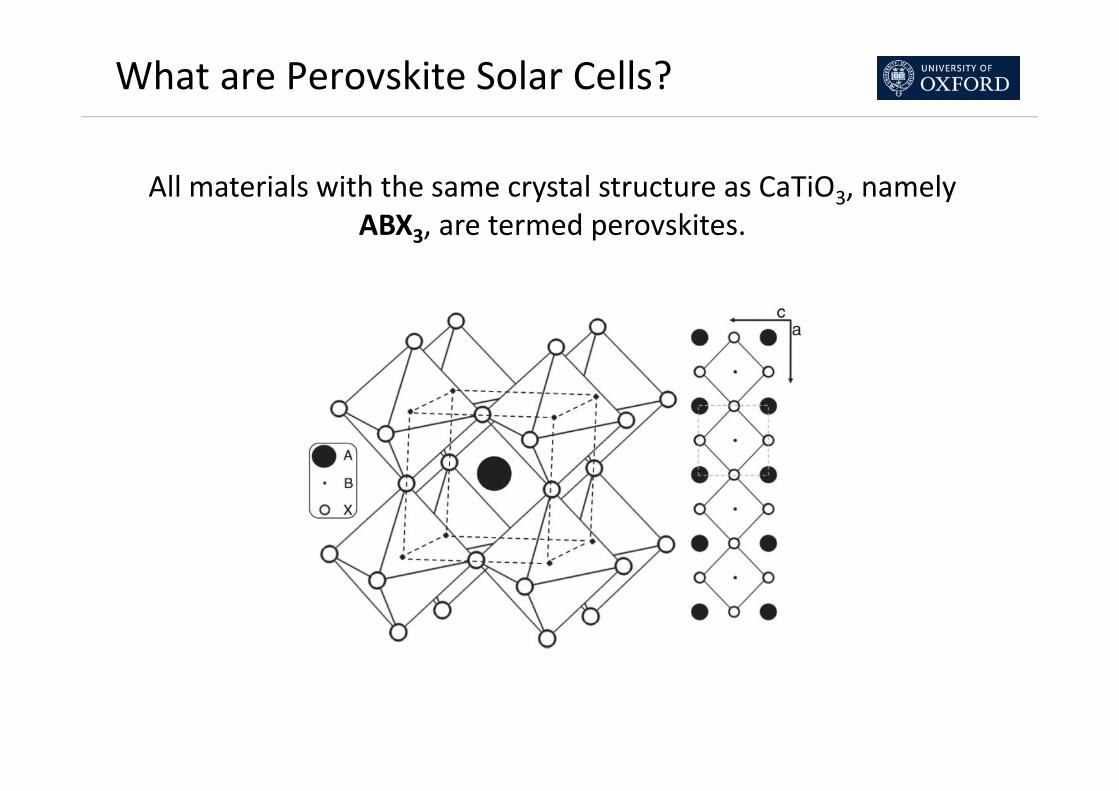
What are Perovskite Solar Cells?
All materials with the same crystal structure as CaTiO3, namely ABX3, are termed perovskites.

Park et al. Nanoscale 2011 Nanoscale, 2011,3, 4088-4093
Tsutomu Miyasaka et al. J. Am. Chem. Soc. 2009, 131, 6050-6051
J. Ball et al. EES 2013
“Quantum dot” absorber to thin film semiconductor
The first examples showed small quantum dots, our route showed highly crystalline thin film

Efficient Planar Heterojunction Solar Cells

Remarkable efficiency rise
1970 1980 1990 2000 2010 20200
10
20
30R
ecor
d ef
ficie
ncy
(%)
Year
GaAs c-Si CIGS CdTe Perovskite

A thin film “double” heterojunction
Compact TiO2
AgSpiro-MeOTAD
Perovskite
FTO
Glass
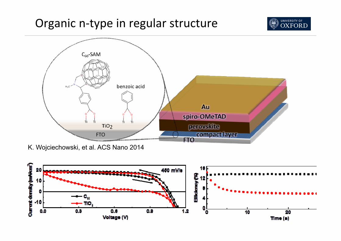
Organic n-type in regular structure
K. Wojciechowski, et al. ACS Nano 2014
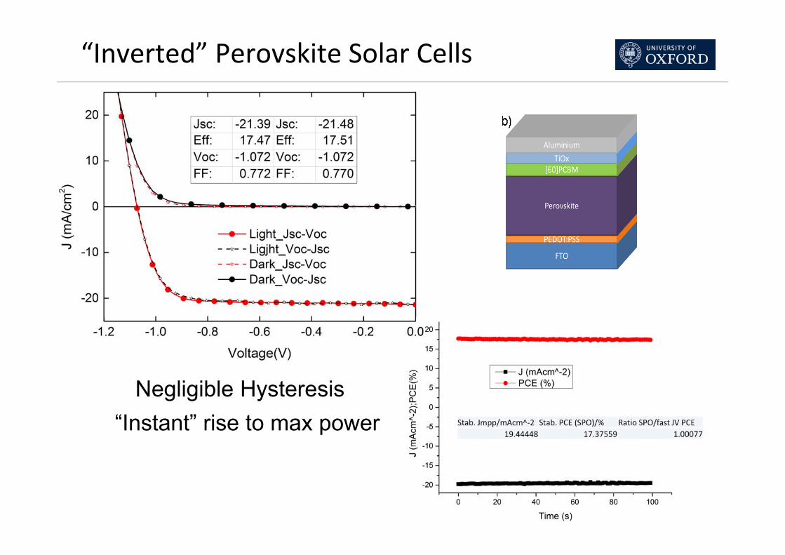
“Inverted” Perovskite Solar Cells
Negligible Hysteresis“Instant” rise to max power

Best architecture for MAPI Cells
J. T-J Wang et al. Submitted

Solar Cell Performance
ControlHPA
HPAControl
Control (FB-SC)Control (SC-FB)HPA (FB-SC)HPA (SC-FB)
ControlHPA
HPAControl
HPA

Perovskite stability
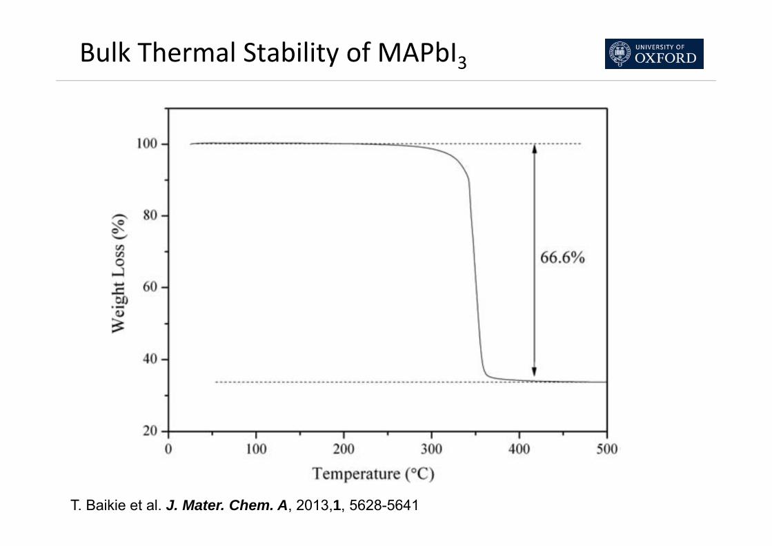
Bulk Thermal Stability of MAPbI3
T. Baikie et al. J. Mater. Chem. A, 2013,1, 5628-5641
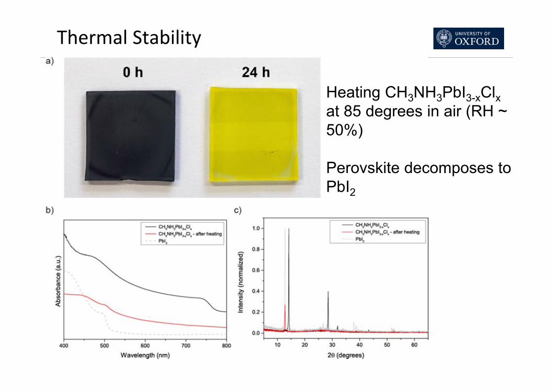
Thermal Stability
Heating CH3NH3PbI3-xClxat 85 degrees in air (RH ~ 50%)
Perovskite decomposes to PbI2

What are the cation options?
Goldshmidt Tolerance factor

FAPbI3Planar Heterojunction Solar cells
0.0 0.2 0.4 0.6 0.8 1.0-5
0
5
10
15
20
25
Jsc = 23.3mAcm-2
Voc = 0.94VFF = 0.65PCE = 14.2%
Cur
rent
den
sity
(mA
cm-2)
Voltage (V)
400 500 600 700 800 9000
20
40
60
80
100
Ext
erna
l Qua
ntum
Effi
cien
cy (%
)
Wavelength (nm)
With Increased pH
Good solar cell operation and red shifted absorption.Loss in voltage a little larger than MAPbI3-xClx, but may be overcome.
G. Eperon et al. EES 2014

Thermal Stability: Formamidinium
@150 ̊C most of the methylamonium CH3NH3 (MA) is lost and the MAPbI3 perovskite PbI2
For Formamidinium, HC(NH2)2+
(FA) the film is stable to heating at 150 ̊C for over an hour in air.

Phase instability of FAPbI3:
Koh, T. M. et al. J Phys Chem C (2013)
Can be overcome by mixing MA with FA, (for instance see Norman Pellet et al. Angew Chem int Ed 2014, 53, 3151) but then still retain thermal instability of MA perovskite.

Economies of Scale
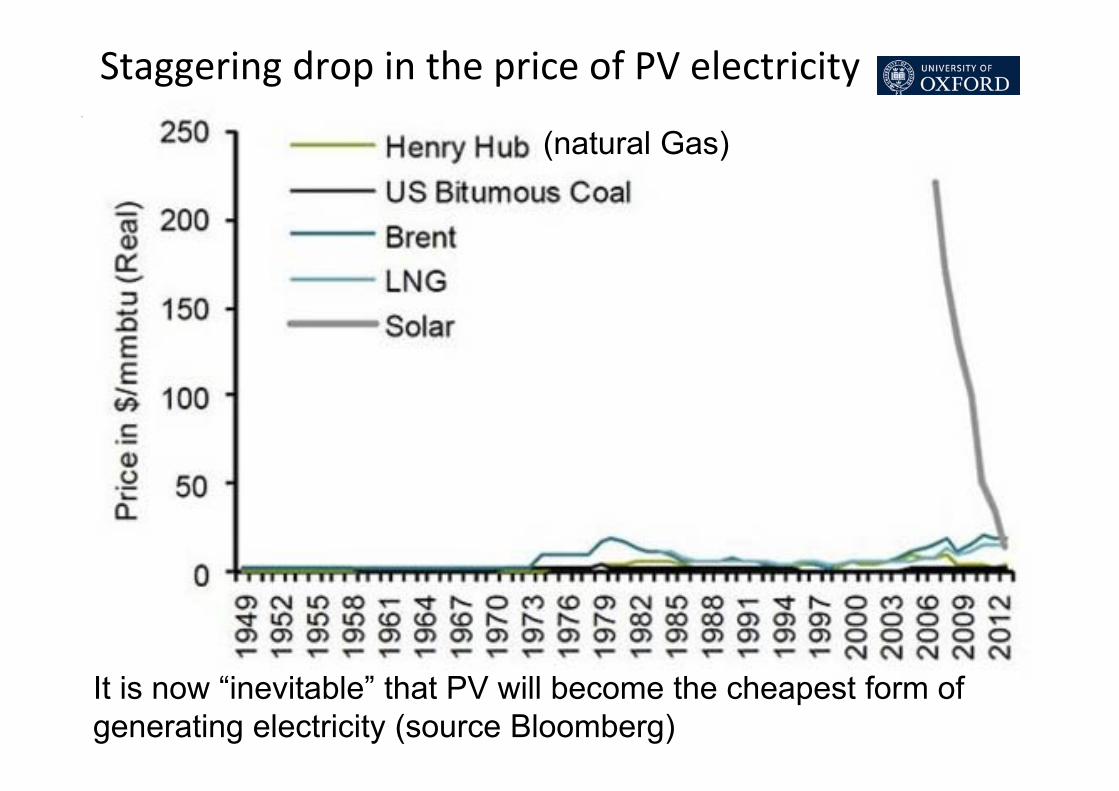
Staggering drop in the price of PV electricity
It is now “inevitable” that PV will become the cheapest form of generating electricity (source Bloomberg)
(natural Gas)

Tandem Solar Cells
Eg. See papers by Baliff et al and McGehee et al,
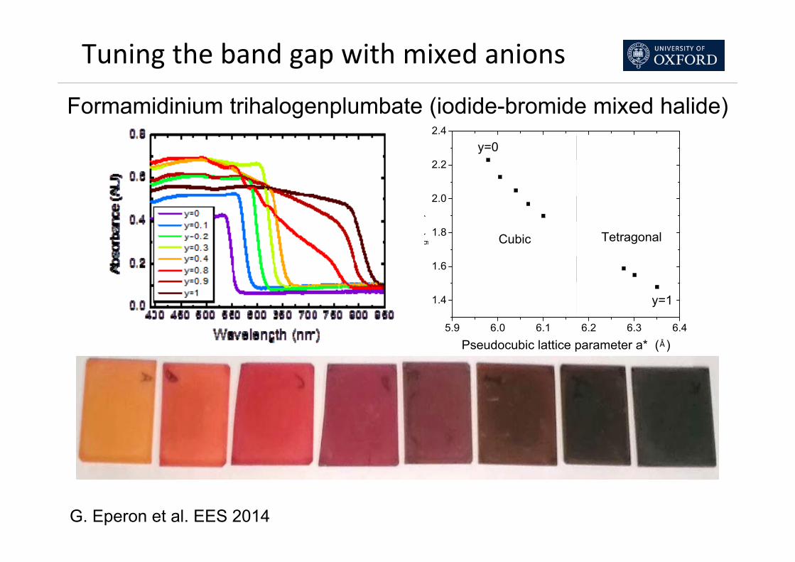
Tuning the band gap with mixed anions
5.9 6.0 6.1 6.2 6.3 6.4
1.4
1.6
1.8
2.0
2.2
2.4
Tetragonal
y=1
Å
g(
)
Pseudocubic lattice parameter a* ( )
y=0
Cubic
G. Eperon et al. EES 2014
Formamidinium trihalogenplumbate (iodide-bromide mixed halide)
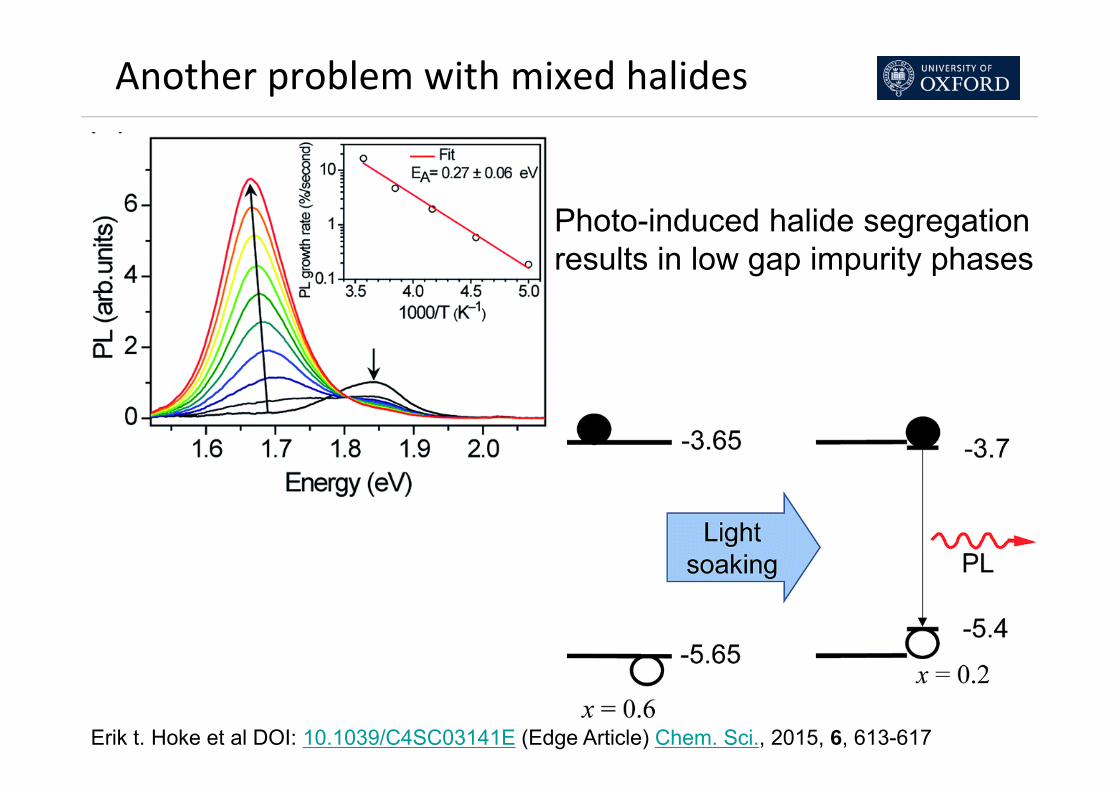
Another problem with mixed halides
Photo-induced halide segregation results in low gap impurity phases
Erik t. Hoke et al DOI: 10.1039/C4SC03141E (Edge Article) Chem. Sci., 2015, 6, 613-617

Adding a small amount of Cs to FAPb(I1-xBrx)3
Ability to crystallise throughout the entire I-Br compositional range

No shift in PL for FA0.83Cs0.17Pb(I0.6Br0.4)
Blasted at 5Wcm-1
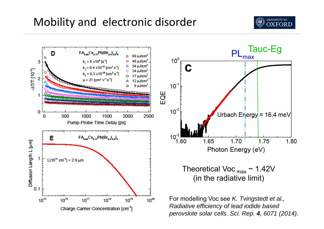
Mobility and electronic disorder
Theoretical Voc max ~ 1.42V(in the radiative limit)
PLmaxTauc-Eg
For modelling Voc see K. Tvingstedt et al., Radiative efficiency of lead iodide based perovskite solar cells. Sci. Rep. 4, 6071 (2014).

Solar cell operation
0.0 0.2 0.4 0.6 0.8 1.0 1.202468
10121416182022
Jsc: 19.4 mA cm-2
Eff: 17.9 %Voc: 1.19 VFF: 78.5 %
Cur
rent
Den
sity
(mA
cm
-2)
Voltage (V)
A
0 2 4 6 8 10 12 14 16 180
10
20
30
40
50
60
N total: 220Median: 13.4Std Dev: 4.5
Sam
ple
Cou
nts
JV PCE (%)
A

Simple 4-T configuration
A
-(p)a-Si:H (~10nm)
(n)c-Si (~200µm)
ITO (80 nm)
(n+)a-Si:H (~30nm)
Al
(i)a-Si:H (<10nm)
(i)a-Si:H (<10nm)
+
Glass
FTO
SnO2/PCBM
Perovskite
Spiro-OMeTAD
ITO
Buffer layer

Performance under simulated sun light
D. McMeekin et al. Science 2016 DOI 10.1126/science.aad5845
All Inorganic Perovskites
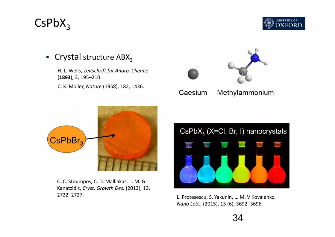
CsPbX3
Crystal structure ABX3
H. L. Wells, Zeitschrift fur Anorg. Chemie (1893), 3, 195–210.
C. K. Moller, Nature (1958), 182, 1436.
CsPbBr3
L. Protesescu, S. Yakunin, … M. V Kovalenko, Nano Lett., (2015), 15 (6), 3692–3696.
C. C. Stoumpos, C. D. Malliakas, … M. G. Kanatzidis, Cryst. Growth Des. (2013), 13, 2722−2727.
34

Introduction to CsPbX3
Thermal stability
Reversible transitions
35
adapted from Sharma et al.
Cubic Perovskite
(Tetragonal)
Orthorhombic non-perovskite phase at RTCsPbBr3
130 °C
CsPbI3316 °C
Phase diagram: S. Sharma, N. Weiden, & A. Weiss, Zeitschrift Für Physikalische Chemie, (1992), 175 (1), 63–80.
Evaporation: S. Kondo, T. Sakai, H. Tanaka, T. Saito, Phys. Rev. B (1998), 58, 11401–11407.

CsPbI3: One-step method
Cubic Perovskite
CubicPm-3m
Black phase
>310oC
OrthorhombicPnma
Yellow phase
CsPbI
Room tempCsPbI3
316 °C
G. E. Eperon, G. M. Paternò, R. J. Sutton, A. Zampetti, A. Haghighirad, F. Cacialli, H. J. Snaith, J. Mater. Chem. A (2015), DOI: 10.1039/C5TA06398A.
G. E. Eperon, G. M. Paternò, R. J. Sutton, A. Zampetti, A. Haghighirad, F. Cacialli, H. Snaith, H. J. Mater. Chem. A (2015), DOI: 10.1039/C5TA06398A.

One-step series: CsPb(IxBr1-x)3
Bandgap is tuneable with bromide content Cubic Perovskite
600 625 650 675 700 725 750 775 8000.0
0.2
0.4
0.6
0.8
1.0
PL
Inte
nsity
(nor
mal
ised
)
Wavelength /nm
x = 1 x = 0.93 x = 0.87 x = 0.8 x = 0.73 x = 0.67
400 450 500 550 600 650 700 750 8000.0
0.5
1.0
1.5
2.0
2.5
Abs
orba
nce
/a.u
.
Wavelength /nm
x = 1 x = 0.93 x = 0.87 x = 0.8 x = 0.73 x = 0.67
1 95c
ba
d

One-step series: CsPb(IxBr1-x)3
38
Wavelength /nm
0.65 0.70 0.75 0.80 0.85 0.90 0.95 1.00
1.75
1.80
1.85
1.90
1.95
y = 2.21 - 0.45 x
c
Abs
orpt
ion
onse
t; P
L pe
ak /e
V
Fractional iodide concentration 'x'
CsPbI2Br1.92 eV
38
Cubic Perovskite
600 625 650 675 700 725 750 775 8000.0
0.2
0.4
0.6
0.8
1.0
PL
Inte
nsity
(nor
mal
ised
)
Wavelength /nm
x = 1 x = 0.93 x = 0.87 x = 0.8 x = 0.73 x = 0.67
400 450 500 550 600 650 700 750 8000.0
0.5
1.0
1.5
2.0
2.5
Abs
orba
nce
/a.u
.
Wavelength /nm
x = 1 x = 0.93 x = 0.87 x = 0.8 x = 0.73 x = 0.67
1 95c
ba
d

CsPbI2Br film properties
350 °C 400 °C250 °C 300 °C
100 °C 150 °C 200 °C
D. M. Trots and S. V. Myagkota, J. Phys. Chem. Solids, (2008), 69 (10), 2520–2526.

Stability in air: CsPbI2Br vs CsPbI3
40 40
0 10 20 30 40 50 60 70 800.2
0.3
0.4
0.5
0.6
0.7d
Abs
orba
nce
/a.u
.
Time /minutes
x = 0.67: CsPbI2Br x = 1: CsPbI3
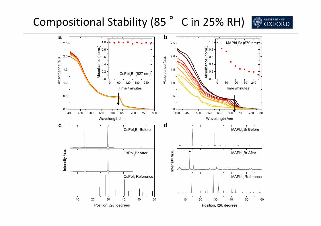
Compositional Stability (85 °C in 25% RH)
400 450 500 550 600 650 700 750 8000.0
0.5
1.0
1.5
2.0
2.5
b
Abs
orba
nce
/a.u
.
Wavelength /nm400 450 500 550 600 650 700 750 800
0.0
0.5
1.0
1.5
2.0
2.5
Abs
orba
nce
/a.u
.
Wavelength /nm
0 60 120 180 2400.0
0.2
0.4
0.6
0.8
1.0
CsPbI2Br (627 nm)
Abs
orba
nce
(nor
m.)
Time /minutes0 60 120 180 240
0.0
0.2
0.4
0.6
0.8
1.0 MAPbI2Br (670 nm)
Abs
orba
nce
(nor
m.)
Time /minutes
a
CsPbI2Br After
10 20 30 40 50 60
Position, /2θ, degrees
CsPbI3 Reference
dc
Inte
nsity
/a.u
.
Inte
nsity
/a.u
.
CsPbI2Br Before MAPbI2Br Before
MAPbI2Br After♦
10 20 30 40 50 60
Position, /2θ, degrees
MAPbI3 Reference
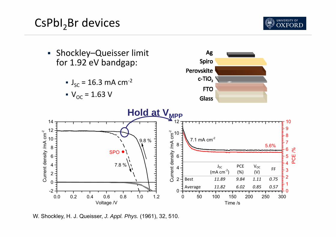
CsPbI2Br devices
Shockley–Queisser limit for 1.92 eV bandgap:
JSC = 16.3 mA cm-2
VOC = 1.63 V
W. Shockley, H. J. Queisser, J. Appl. Phys. (1961), 32, 510.
0.0 0.2 0.4 0.6 0.8 1.0 1.2-2
0
2
4
6
8
10
12
14
7.8 %
Cur
rent
den
sity
/mA
cm-2
Voltage /V
9.8 %
SPO
c
0
2
4
6
8
10
12
Time /s
Cur
rent
den
sity
/mA
cm
-2
5.6%7.1 mA cm-2
JSC (mA cm-2)
PCE (%)
VOC (V) FF
Best 11.89 9.84 1.11 0.75
Average 11.82 6.02 0.85 0.57
0 50 100 150 200 250 300012345678910
PC
E /%
dHold at VMPP

Commercialisation

Device and mini-module development Target: Develop stable and efficient materials stack
Develop processing methodology to deliver
Efficient perovskite/Silicon tandem cells at
high yield
Partner with existing Si-PV industry to
manufacture

Targeted Market
Combining Perovskites and Si in a tandem architecture could lead to >30% efficient modules
Example of possible structure
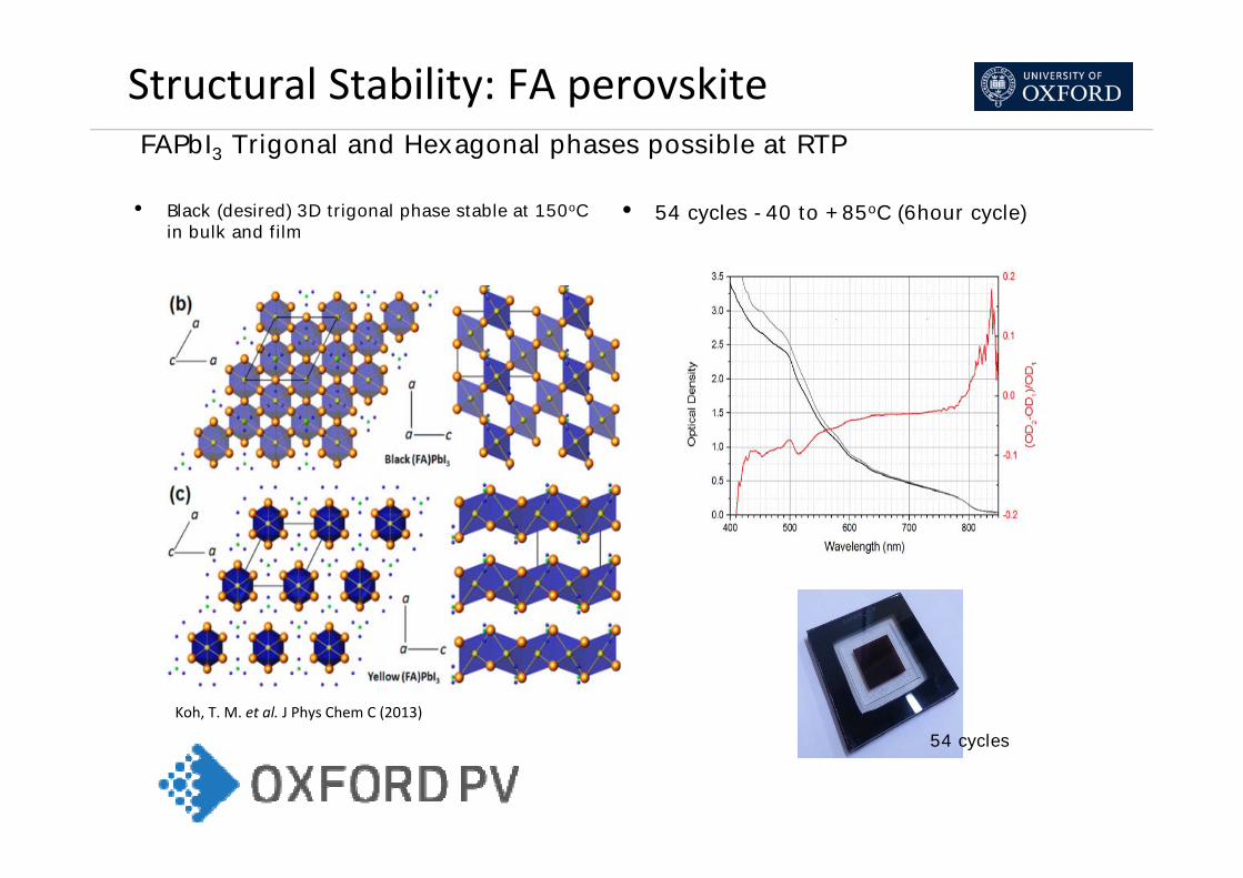
Structural Stability: FA perovskiteFAPbI3 Trigonal and Hexagonal phases possible at RTP
• Black (desired) 3D trigonal phase stable at 150oC in bulk and film
Koh, T. M. et al. J Phys Chem C (2013)
• 54 cycles -40 to +85oC (6hour cycle)
54 cycles
0
20
40
60
80
100
120
-300 200 700 1200
Nor
mal
ised
pero
vski
te C
olou
rIn
tens
ity (%
)
Stressing Time (hours)
Control(140)Control(115)A
B
C
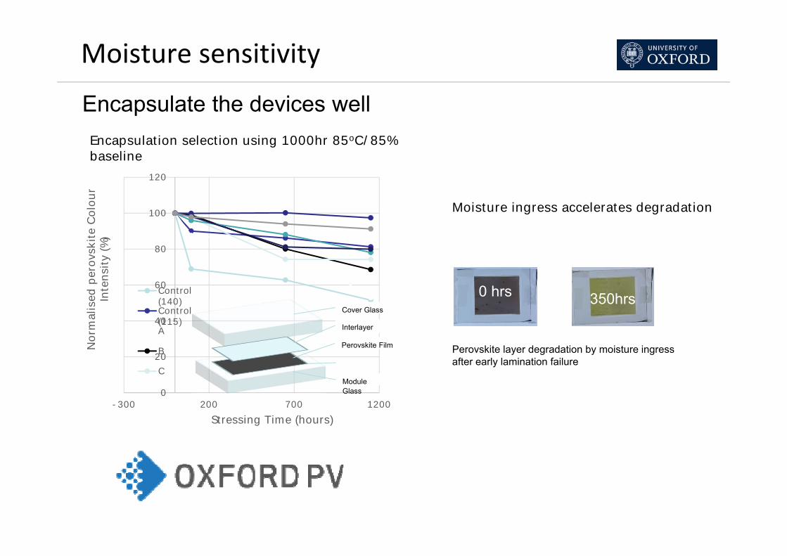
Moisture sensitivity
Interlayer assembly only
Encapsulation selection using 1000hr 85oC/85% baseline
Perovskite layer degradation by moisture ingress after early lamination failure
350hrs0 hrs
Moisture ingress accelerates degradation
Cover Glass
Interlayer
Perovskite Film
Module Glass
Encapsulate the devices well

Full sun light soaking 60⁰ C
0
0.2
0.4
0.6
0.8
1
1.2
1.4
1.6
0 500 1000 1500 2000
Nor
mal
ised
Pm
ax
Hours elapsed
Solar cells aged under load with no UV filter at 60 ⁰C
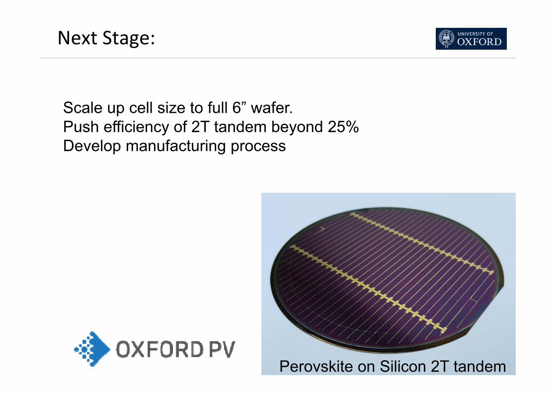
Next Stage:
Scale up cell size to full 6” wafer.Push efficiency of 2T tandem beyond 25%Develop manufacturing process
Perovskite on Silicon 2T tandem

How do perovskites compare to other technologies?
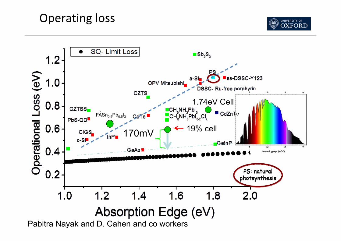
Operating loss
19% cell170mV
Pabitra Nayak and D. Cahen and co workers
FASn0.5Pb0.5I3
1.74eV Cell

Acknowledgements
Funding EPSRC, ERC & FP7, Oxford John Fell Fund, Oxford Martin School, Royal Society.
Collaborators:Perovskites:Takuru MurakamiTsutomu Miyasaka
Oxford:Michael JohnstonLaura HerzRobin NicholasVictor BurlakovAlan Goriely
Swansea: David Worsley, Tristan Watson et al.
Milan:Annamaria PetrozzaGiulia Grancini et al.
Cambridge: Richard FriendFelix Deschler Michael PriceAditiya et al.
ICL Franco Cacialli
Helholtz:Lars KorteBernd Reiche
LoughboroughPatrick IsherwoodMike Walls
+ others