mems vertical probe cards with ultra densely arrayed metal ...orbit.dtu.dk/files/4337225/fei.pdf ·...
TRANSCRIPT
General rights Copyright and moral rights for the publications made accessible in the public portal are retained by the authors and/or other copyright owners and it is a condition of accessing publications that users recognise and abide by the legal requirements associated with these rights.
• Users may download and print one copy of any publication from the public portal for the purpose of private study or research. • You may not further distribute the material or use it for any profit-making activity or commercial gain • You may freely distribute the URL identifying the publication in the public portal
If you believe that this document breaches copyright please contact us providing details, and we will remove access to the work immediately and investigate your claim.
Downloaded from orbit.dtu.dk on: May 28, 2018
MEMS Vertical Probe Cards With Ultra Densely Arrayed Metal Probes for Wafer-LevelIC Testing
Wang, Fei; Cheng, Rong; Li, Xinxin
Published in:I E E E Journal of Microelectromechanical Systems
Link to article, DOI:10.1109/JMEMS.2009.2021815
Publication date:2009
Document VersionPublisher's PDF, also known as Version of record
Link back to DTU Orbit
Citation (APA):Wang, F., Cheng, R., & Li, X. (2009). MEMS Vertical Probe Cards With Ultra Densely Arrayed Metal Probesfor Wafer-Level IC Testing. I E E E Journal of Microelectromechanical Systems, 18(4), 933-941. DOI:10.1109/JMEMS.2009.2021815
JOURNAL OF MICROELECTROMECHANICAL SYSTEMS, VOL. 18, NO. 4, AUGUST 2009 933
MEMS Vertical Probe Cards With Ultra DenselyArrayed Metal Probes for Wafer-Level IC Testing
Fei Wang, Member, IEEE, Rong Cheng, and Xinxin Li
Abstract—We have developed a MEMS probe-card technologyfor wafer-level testing ICs with 1-D line-arrayed or 2-D area-arrayed dense pads layouts. With a novel metal MEMS fabricationtechnique, an area-arrayed tip matrix is realized with an ultra-dense tip pitch of 90 μm × 196 μm for testing 2-D pad layout,and a 50-μm minimum pitch is also achieved in line-arrayed probecards for testing line-on-center or line-on-perimeter wafers. By us-ing the anisotropic etching properties of single-crystalline silicon,novel oblique concave cavities are formed as electroplating mouldsfor the area-arrayed microprobes. With the micromachined cavitymoulds, the probes are firstly electroplated in a silicon wafer andfurther flip-chip packaged onto a low-temperature cofired ceramicboard for signal feeding to an automatic testing equipment. Themicroprobes can be efficiently released using a silicon-loss tech-nique with a lateral underneath etching. The measured materialproperties of the electroplated nickel and the Sn–Ag solder bumpare promising for IC testing applications. Mechanical tests haveverified that the microprobes can withstand a 65-mN probingforce, while the tip displacement is 25 μm, and can reliably workfor more than 100 000 touchdowns. The electric test shows that theprobe array can provide a low contact resistance of below 1 Ω,while the current leakage is only 150 pA at 3.3 V for adjacentprobes. [2008-0273]
Index Terms—Dense-arrayed vertical tips, electroplating,IC testing, micromachining, probe card.
I. INTRODUCTION
WAFER-LEVEL IC testing has been an integral part ofthe IC manufacturing processes for over four decades
[1]. Yet, its significance has only just been properly regardedwith the recent dazzling development of microelectronic pack-aging technologies. Advanced concepts, such as multichipmodule, system-on-chip, system-in-package, and system-on-package, will eventually change electronic products into “con-vergent systems” that consist of computation, communication,consumer, and even biomedical functions [2]. This revolution-
Manuscript received November 5, 2008; revised April 9, 2009. First pub-lished June 16, 2009; current version published July 31, 2009. This work wassupported in part by the NSFC Project (60725414) and in part by the Chinese973 Program (2006CB300405). The work of X. Li was supported by Na-tional Natural Science Foundation of China Project 60721004. Subject EditorG. K. Fedder.
F. Wang was with the State Key Laboratory of Transducer Technology,Shanghai Institute of Microsystem and Information Technology, Chinese Acad-emy of Sciences, Shanghai 200050, China. He is now with the Departmentof Micro- and Nanotechnology, Technical University of Denmark, DK-2800Lyngby, Denmark.
R. Cheng and X. Li are with the State Key Laboratory of Transducer Technol-ogy, Shanghai Institute of Microsystem and Information Technology, ChineseAcademy of Sciences, Shanghai 200050, China (e-mail: [email protected]).
Color versions of one or more of the figures in this paper are available onlineat http://ieeexplore.ieee.org.
Digital Object Identifier 10.1109/JMEMS.2009.2021815
ary movement of multisystem integration has greatly chal-lenged the wafer-level testing technology in two ways. First,it demands a much higher testing yield for known-good-die(KGD), since any fault of one subsystem or chip would ruin thewhole system. On the other hand, it brings a trend that the end-of-line (EOL) processes cost more and play a more importantrole in the whole IC manufacturing processes than the front-of-line (FOL) processes. Therefore, the wafer-level IC testing,which is a wafer test between EOL and FOL, has become moreimportant than before for high-yield and low-cost production ofKGD [3].
During wafer-level IC testing, probe cards are utilized as theprincipal interface for signal routing between the dies undertest (DUT) and the automatic test equipment (ATE), to pass orfail the DUT. Recently, many MEMS probe cards have beendeveloped [4]–[13], some of which have been commercializedbecause of their great advantages over conventional probecards [4]. The conventional probe card, which is an epoxyring manually mounted with tens to hundreds of cantileverneedles, would not be adaptable for the next-generation ICtesting because of its own limitations. “Moore’s Law” has beenstimulating continually increasing pad density and narrowingpad pitch, which is now challenging the limitations of man-ual assembly capability. For testing high-speed circuits, signalcrosstalk and parasitic inductance also make the epoxy probecards difficult to adapt. Moreover, the cost of an epoxy probecard usually ranges from 1 k to 10 k or even higher dependingon the number of needles. In contrast, MEMS probe cardsuse integrating technologies that are in favor of enhancingthe tip uniformity and fabricating high-density probe arrays atlower cost. Furthermore, MEMS probe cards are promising forhigh-speed ICs because of their excellent compatibility withIC fabrication. Not surprisingly, advanced probe cards basedon MEMS technologies have been accepted as a promisingcandidate for next-generation IC testing tools.
However, some of the previous attempts have their ownlimitations. For example, the membrane probe card needs anextra gas pressure system, which increases the complexityof the ATE system. Moreover, all the probes cannot contactthe DUT simultaneously, since probe deflection is nonuniformacross the membrane [5]. The previously developed thermallyactuated bimorph microprobes can only provide a probing forceof 45–60 μN, which is too small to break the natural oxideon the surface of the Al pads [6]. In addition, for this ther-mally actuated method, heating signal lines are needed, whichmeans that the total number of lead-out lines is doubled. Manycantilever-tip-type probe cards have been developed which have
1057-7157/$26.00 © 2009 IEEE
Authorized licensed use limited to: Danmarks Tekniske Informationscenter. Downloaded on May 10,2010 at 09:14:21 UTC from IEEE Xplore. Restrictions apply.

934 JOURNAL OF MICROELECTROMECHANICAL SYSTEMS, VOL. 18, NO. 4, AUGUST 2009
Fig. 1. Comparison of tip pitch among the reported “hoe”-shaped probes [in (a)] and the two probe cards proposed in this paper [with the line-arrayed probes in(b) and the area-arrayed probes in (c)].
a stiffer structure and can withstand a much larger probingforce [7]–[10]. The cantilever probes can be densely arrayedin one direction and feature fine tip pitch less than 100 μm.Unfortunately, the cantilever structure usually takes more thanhundreds of micrometers to 1 mm in the perpendicular direc-tion to the tip array. Thus, they are only suitable for testingconventional in-line devices, such as memory devices in whichtesting pads are simply line-arrayed with the perimeter or line-on-center (LOC) configuration. Recently, 1- and 2-D arrayedpad layouts have been widely used in advanced devices, suchas LCD-driver ICs and the wafers with pad redistribution, sinceIBM developed the controlled collapse chip connection (C4)process [11]. Many microspring structures have been fabricatedwith electroplating techniques for various applications, such asa measurement system for contacts [14], small-pitch flip-chippackaging [15], and a platform for high-frequency testing [16].Based on multilayer electroplating techniques, a microspringprobe card has been recently developed for C4 design [12].Unfortunately, the fabrication demands a fussy process of fiveto seven separate electroplating steps that is not easily imple-mented. Moreover, the probes exhibit a spatial tip pitch, and itis difficult to test the device with the pitch less than 200 μm.
In this paper, we present a new type of MEMS probe card, inwhich both highly dense line-arrayed and area-arrayed nickeltips can be fabricated simultaneously in a same wafer. Witha novel oblique silicon cavity mould by a unique etchingtechnique, the nickel microprobes are, for the first time, elec-troplated on an inclined surface and further flip-chip bonded toa low-temperature cofired ceramic (LTCC) substrate via Sn–Agsolder bumps. Then, the probes can be high-yield released witha silicon-loss technique. With this method, the vertical metalprobes can be densely arrayed in two dimensions. The detailedtechnique is described in the following sections.
II. DESIGN AND SIMULATION
The authors previously developed a MEMS probe card with“hoe”-shaped metal tips [17]. As shown in Fig. 1(a), the mi-croprobe has a large footprint and features a 2-D tip pitchof 240 μm × 160 μm. The tip pitch is still larger than thatdemanded in many dense-pad IC testing applications. In thispaper, we propose a much more compact structure that canbe easily arrayed in either 1-D line or 2-D area. The top-view
schematic is shown in Fig. 1(b). When the nickel electroplatingis performed within a regular silicon anisotropic etching formedcavity, the “face-to-face” probe design can shrink the two-rowor one-row line-arrayed tip pitch down to 35 μm. This type ofprobe card can be used for testing LOC devices or the multi-DUT testing. As for the dies with area-arrayed pads, densely2-D arrayed microprobes will be formed with a novel oblique-cavity mould etching technique. As schematically shown inFig. 1(c), the “face-to-face” two-row layout can be changed toa “one-after-one” design. The tip pitch of the former “face-to-face” design used two inclined walls from anisotropic etching.In contrast, the tip pitch in the “one-after-one” design canbe much compressed, because the etched silicon cavity onlycontains one inclined sidewall for probe electroplating. It canbe seen clearly from Fig. 1 that the area-arrayed tip pitch canbe further shrunk to 90 μm × 196 μm for ultradense 2-D padlayout. By using this novel area-arrayed technique and the line-arrayed one, probe cards with various tip-array layouts can berealized with the vertical metal probe fabrication techniques fortesting various types of DUT.
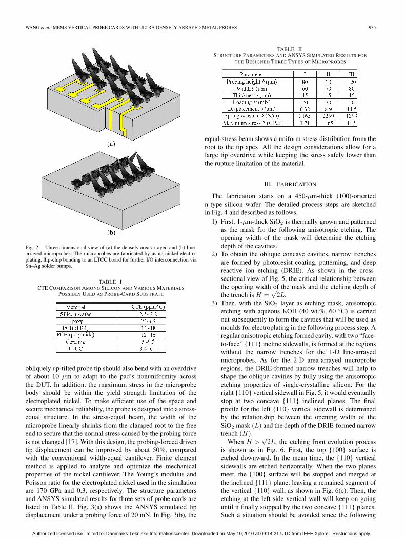
The 3-D views in Fig. 2 show the designed structure of themicroprobe arrays. Both the line-arrayed and the area-arrayedprobe cards are fabricated using similar processes. The verticalmicroprobes are first selectively electroplated in silicon cavitymoulds that were previously formed by anisotropic etching ina silicon wafer and then flip-chip bonded to an LTCC boardfor backside I/O interconnection with ATE. Compared withconventional probe cards where postpackaging or assembly wasused [13], the flip-chip bonding technique is a more efficientmethod to simultaneously transfer the thousands of micro-probes. The LTCC board provides a rigid substrate for the probecards, which can withstand a total force of about 1–10 kg, sincethe contact force of each microprobe can be around 1–10 g.More importantly, the LTCC board and the silicon IC waferhave close values for coefficient of thermal expansion (CTE)that guarantees a small mismatch between the probe tips and thepads under test, even when used in a high-temperature burn-intest. Table I shows the comparison in CTE among silicon andother materials possibly used for probe-card substrate [18].
During wafer-level testing, the probe tips are forced tocontact with the pads of the DUT and have to withstanda typical probing force of about 10 mN to achieve a lowcontact resistance between the tip and the pad. Meanwhile, the
Authorized licensed use limited to: Danmarks Tekniske Informationscenter. Downloaded on May 10,2010 at 09:14:21 UTC from IEEE Xplore. Restrictions apply.
WANG et al.: MEMS VERTICAL PROBE CARDS WITH ULTRA DENSELY ARRAYED METAL PROBES 935
Fig. 2. Three-dimensional view of (a) the densely area-arrayed and (b) line-arrayed microprobes. The microprobes are fabricated by using nickel electro-plating, flip-chip bonding to an LTCC board for further I/O interconnection viaSn–Ag solder bumps.
TABLE ICTE COMPARISON AMONG SILICON AND VARIOUS MATERIALS
POSSIBLY USED AS PROBE-CARD SUBSTRATE
obliquely up-tilted probe tip should also bend with an overdriveof about 10 μm to adapt to the pad’s nonuniformity acrossthe DUT. In addition, the maximum stress in the microprobebody should be within the yield strength limitation of theelectroplated nickel. To make efficient use of the space andsecure mechanical reliability, the probe is designed into a stress-equal structure. In the stress-equal beam, the width of themicroprobe linearly shrinks from the clamped root to the freeend to secure that the normal stress caused by the probing forceis not changed [17]. With this design, the probing-forced driventip displacement can be improved by about 50%, comparedwith the conventional width-equal cantilever. Finite elementmethod is applied to analyze and optimize the mechanicalproperties of the nickel cantilever. The Young’s modulus andPoisson ratio for the electroplated nickel used in the simulationare 170 GPa and 0.3, respectively. The structure parametersand ANSYS simulated results for three sets of probe cards arelisted in Table II. Fig. 3(a) shows the ANSYS simulated tipdisplacement under a probing force of 20 mN. In Fig. 3(b), the
TABLE IISTRUCTURE PARAMETERS AND ANSYS SIMULATED RESULTS FOR
THE DESIGNED THREE TYPES OF MICROPROBES
equal-stress beam shows a uniform stress distribution from theroot to the tip apex. All the design considerations allow for alarge tip overdrive while keeping the stress safely lower thanthe rupture limitation of the material.
III. FABRICATION
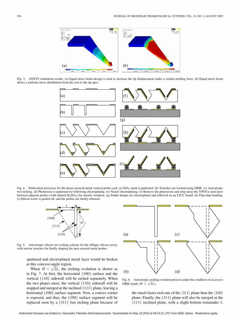
The fabrication starts on a 450-μm-thick (100)-orientedn-type silicon wafer. The detailed process steps are sketchedin Fig. 4 and described as follows.
1) First, 1-μm-thick SiO2 is thermally grown and patternedas the mask for the following anisotropic etching. Theopening width of the mask will determine the etchingdepth of the cavities.
2) To obtain the oblique concave cavities, narrow trenchesare formed by photoresist coating, patterning, and deepreactive ion etching (DRIE). As shown in the cross-sectional view of Fig. 5, the critical relationship betweenthe opening width of the mask and the etching depth ofthe trench is H =
√2L.
3) Then, with the SiO2 layer as etching mask, anisotropicetching with aqueous KOH (40 wt.%, 60 ◦C) is carriedout subsequently to form the cavities that will be used asmoulds for electroplating in the following process step. Aregular anisotropic etching formed cavity, with two “face-to-face” {111} incline sidewalls, is formed at the regionswithout the narrow trenches for the 1-D line-arrayedmicroprobes. As for the 2-D area-arrayed microproberegions, the DRIE-formed narrow trenches will help toshape the oblique cavities by fully using the anisotropicetching properties of single-crystalline silicon. For theright {110} vertical sidewall in Fig. 5, it would eventuallystop at two concave {111} inclined planes. The finalprofile for the left {110} vertical sidewall is determinedby the relationship between the opening width of theSiO2 mask (L) and the depth of the DRIE-formed narrowtrench (H).
When H >√
2L, the etching front evolution processis shown as in Fig. 6. First, the top {100} surface isetched downward. In the mean time, the {110} verticalsidewalls are etched horizontally. When the two planesmeet, the {100} surface will be stopped and merged atthe inclined {111} plane, leaving a remained segment ofthe vertical {110} wall, as shown in Fig. 6(c). Then, theetching at the left-side vertical wall will keep on goinguntil it finally stopped by the two concave {111} planes.Such a situation should be avoided since the following
Authorized licensed use limited to: Danmarks Tekniske Informationscenter. Downloaded on May 10,2010 at 09:14:21 UTC from IEEE Xplore. Restrictions apply.
936 JOURNAL OF MICROELECTROMECHANICAL SYSTEMS, VOL. 18, NO. 4, AUGUST 2009
Fig. 3. ANSYS simulation results. (a) Equal-stress beam design is used to increase the tip displacement under a certain probing force. (b) Equal-stress beamshows a uniform stress distribution from the root to the tip apex.
Fig. 4. Fabrication processes for the dense-arrayed metal vertical probe card. (a) SiO2 mask is patterned. (b) Trenches are formed using DRIE. (c) Anisotropicwet etching. (d) Photoresist is patterned for following electroplating. (e) Nickel electroplating. (f) Remove the photoresist and strip away the TiW/Cu seed layerbetween adjacent probes (with diluted H2SO4) for electric isolation. (g) Solder bumps are electroplated and reflowed on an LTCC board. (h) Flip-chip bonding.(i) Silicon wafer is peeled off, and the probes are finally released.
Fig. 5. Anisotropic silicon wet etching scheme for the oblique silicon cavity,with narrow trenches for finally shaping the area-arrayed metal probes.
sputtered and electroplated metal layer would be brokenat this concave-angle region.
When H <√
2L, the etching evolution is shown asin Fig. 7. At first, the horizontal {100} surface and thevertical {110} sidewall will be etched separately. Whenthe two planes meet, the vertical {110} sidewall will bestopped and merged at the inclined {111} plane, leaving ahorizontal {100} surface segment. Now, a convex corneris exposed, and thus, the {100} surface segment will bereplaced soon by a {311} fast etching plane because of
Fig. 6. Anisotropic etching evolution process under the condition of excessiveDRIE depth (H >
√2L).
the much faster etch rate of the 〈311〉 plane than the 〈100〉plane. Finally, the {311} plane will also be merged at the{111} inclined plane, with a slight bottom remainder δ,
Authorized licensed use limited to: Danmarks Tekniske Informationscenter. Downloaded on May 10,2010 at 09:14:21 UTC from IEEE Xplore. Restrictions apply.
WANG et al.: MEMS VERTICAL PROBE CARDS WITH ULTRA DENSELY ARRAYED METAL PROBES 937
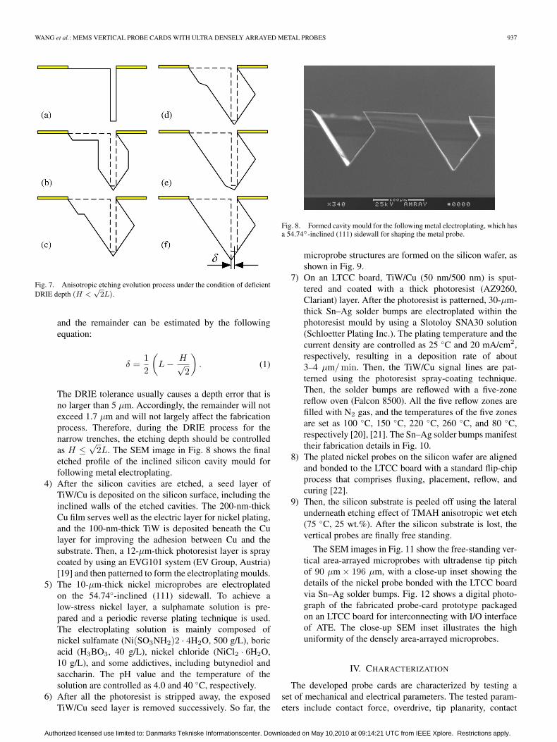
Fig. 7. Anisotropic etching evolution process under the condition of deficientDRIE depth (H <
√2L).
and the remainder can be estimated by the followingequation:
δ =12
(L − H√
2
). (1)
The DRIE tolerance usually causes a depth error that isno larger than 5 μm. Accordingly, the remainder will notexceed 1.7 μm and will not largely affect the fabricationprocess. Therefore, during the DRIE process for thenarrow trenches, the etching depth should be controlledas H ≤
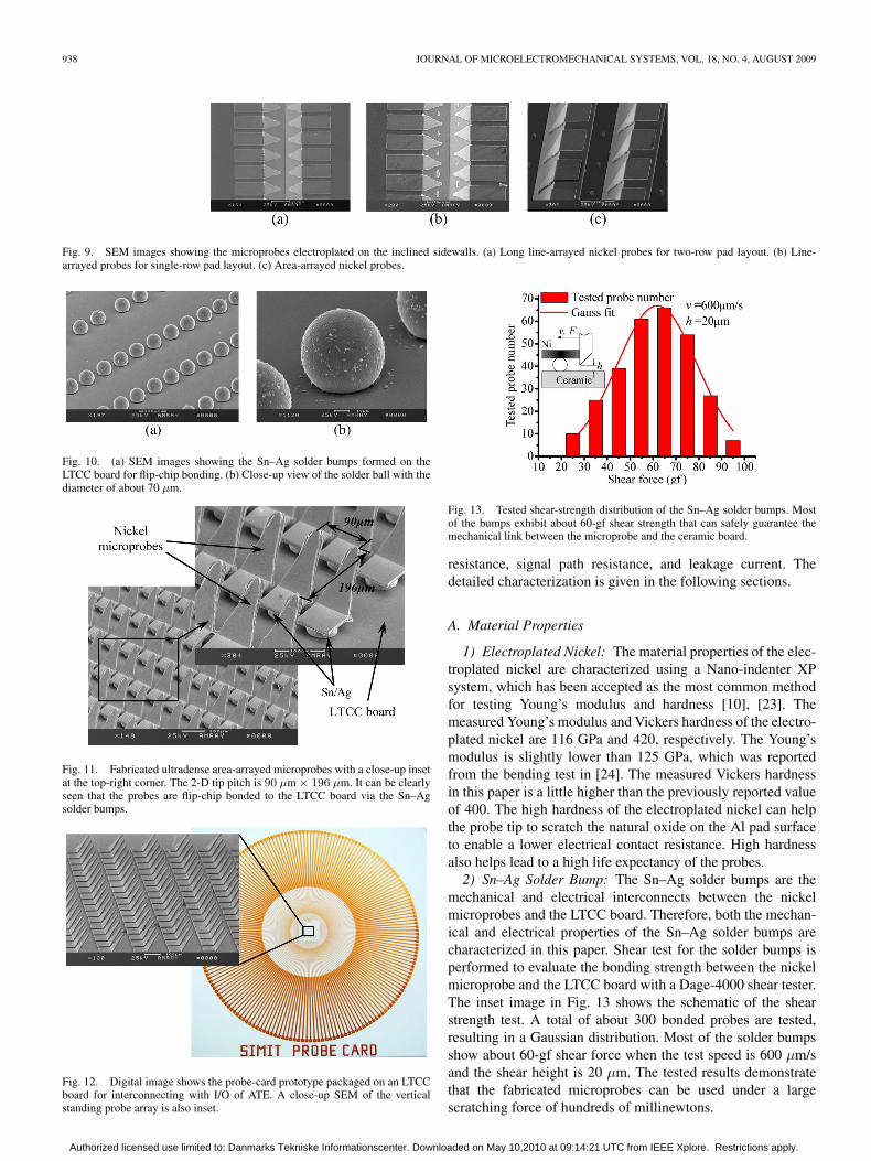
√2L. The SEM image in Fig. 8 shows the final
etched profile of the inclined silicon cavity mould forfollowing metal electroplating.
4) After the silicon cavities are etched, a seed layer ofTiW/Cu is deposited on the silicon surface, including theinclined walls of the etched cavities. The 200-nm-thickCu film serves well as the electric layer for nickel plating,and the 100-nm-thick TiW is deposited beneath the Culayer for improving the adhesion between Cu and thesubstrate. Then, a 12-μm-thick photoresist layer is spraycoated by using an EVG101 system (EV Group, Austria)[19] and then patterned to form the electroplating moulds.
5) The 10-μm-thick nickel microprobes are electroplatedon the 54.74◦-inclined (111) sidewall. To achieve alow-stress nickel layer, a sulphamate solution is pre-pared and a periodic reverse plating technique is used.The electroplating solution is mainly composed ofnickel sulfamate (Ni(SO3NH2)2 · 4H2O, 500 g/L), boricacid (H3BO3, 40 g/L), nickel chloride (NiCl2 · 6H2O,10 g/L), and some addictives, including butynediol andsaccharin. The pH value and the temperature of thesolution are controlled as 4.0 and 40 ◦C, respectively.
6) After all the photoresist is stripped away, the exposedTiW/Cu seed layer is removed successively. So far, the
Fig. 8. Formed cavity mould for the following metal electroplating, which hasa 54.74◦-inclined (111) sidewall for shaping the metal probe.
microprobe structures are formed on the silicon wafer, asshown in Fig. 9.
7) On an LTCC board, TiW/Cu (50 nm/500 nm) is sput-tered and coated with a thick photoresist (AZ9260,Clariant) layer. After the photoresist is patterned, 30-μm-thick Sn–Ag solder bumps are electroplated within thephotoresist mould by using a Slotoloy SNA30 solution(Schloetter Plating Inc.). The plating temperature and thecurrent density are controlled as 25 ◦C and 20 mA/cm2,respectively, resulting in a deposition rate of about3–4 μm/min. Then, the TiW/Cu signal lines are pat-terned using the photoresist spray-coating technique.Then, the solder bumps are reflowed with a five-zonereflow oven (Falcon 8500). All the five reflow zones arefilled with N2 gas, and the temperatures of the five zonesare set as 100 ◦C, 150 ◦C, 220 ◦C, 260 ◦C, and 80 ◦C,respectively [20], [21]. The Sn–Ag solder bumps manifesttheir fabrication details in Fig. 10.
8) The plated nickel probes on the silicon wafer are alignedand bonded to the LTCC board with a standard flip-chipprocess that comprises fluxing, placement, reflow, andcuring [22].
9) Then, the silicon substrate is peeled off using the lateralunderneath etching effect of TMAH anisotropic wet etch(75 ◦C, 25 wt.%). After the silicon substrate is lost, thevertical probes are finally free standing.
The SEM images in Fig. 11 show the free-standing ver-tical area-arrayed microprobes with ultradense tip pitchof 90 μm × 196 μm, with a close-up inset showing thedetails of the nickel probe bonded with the LTCC boardvia Sn–Ag solder bumps. Fig. 12 shows a digital photo-graph of the fabricated probe-card prototype packagedon an LTCC board for interconnecting with I/O interfaceof ATE. The close-up SEM inset illustrates the highuniformity of the densely area-arrayed microprobes.
IV. CHARACTERIZATION
The developed probe cards are characterized by testing aset of mechanical and electrical parameters. The tested param-eters include contact force, overdrive, tip planarity, contact
Authorized licensed use limited to: Danmarks Tekniske Informationscenter. Downloaded on May 10,2010 at 09:14:21 UTC from IEEE Xplore. Restrictions apply.
938 JOURNAL OF MICROELECTROMECHANICAL SYSTEMS, VOL. 18, NO. 4, AUGUST 2009
Fig. 9. SEM images showing the microprobes electroplated on the inclined sidewalls. (a) Long line-arrayed nickel probes for two-row pad layout. (b) Line-arrayed probes for single-row pad layout. (c) Area-arrayed nickel probes.
Fig. 10. (a) SEM images showing the Sn–Ag solder bumps formed on theLTCC board for flip-chip bonding. (b) Close-up view of the solder ball with thediameter of about 70 μm.
Fig. 11. Fabricated ultradense area-arrayed microprobes with a close-up insetat the top-right corner. The 2-D tip pitch is 90 μm × 196 μm. It can be clearlyseen that the probes are flip-chip bonded to the LTCC board via the Sn–Agsolder bumps.
Fig. 12. Digital image shows the probe-card prototype packaged on an LTCCboard for interconnecting with I/O of ATE. A close-up SEM of the verticalstanding probe array is also inset.
Fig. 13. Tested shear-strength distribution of the Sn–Ag solder bumps. Mostof the bumps exhibit about 60-gf shear strength that can safely guarantee themechanical link between the microprobe and the ceramic board.
resistance, signal path resistance, and leakage current. Thedetailed characterization is given in the following sections.
A. Material Properties
1) Electroplated Nickel: The material properties of the elec-troplated nickel are characterized using a Nano-indenter XPsystem, which has been accepted as the most common methodfor testing Young’s modulus and hardness [10], [23]. Themeasured Young’s modulus and Vickers hardness of the electro-plated nickel are 116 GPa and 420, respectively. The Young’smodulus is slightly lower than 125 GPa, which was reportedfrom the bending test in [24]. The measured Vickers hardnessin this paper is a little higher than the previously reported valueof 400. The high hardness of the electroplated nickel can helpthe probe tip to scratch the natural oxide on the Al pad surfaceto enable a lower electrical contact resistance. High hardnessalso helps lead to a high life expectancy of the probes.
2) Sn–Ag Solder Bump: The Sn–Ag solder bumps are themechanical and electrical interconnects between the nickelmicroprobes and the LTCC board. Therefore, both the mechan-ical and electrical properties of the Sn–Ag solder bumps arecharacterized in this paper. Shear test for the solder bumps isperformed to evaluate the bonding strength between the nickelmicroprobe and the LTCC board with a Dage-4000 shear tester.The inset image in Fig. 13 shows the schematic of the shearstrength test. A total of about 300 bonded probes are tested,resulting in a Gaussian distribution. Most of the solder bumpsshow about 60-gf shear force when the test speed is 600 μm/sand the shear height is 20 μm. The tested results demonstratethat the fabricated microprobes can be used under a largescratching force of hundreds of millinewtons.
Authorized licensed use limited to: Danmarks Tekniske Informationscenter. Downloaded on May 10,2010 at 09:14:21 UTC from IEEE Xplore. Restrictions apply.
WANG et al.: MEMS VERTICAL PROBE CARDS WITH ULTRA DENSELY ARRAYED METAL PROBES 939
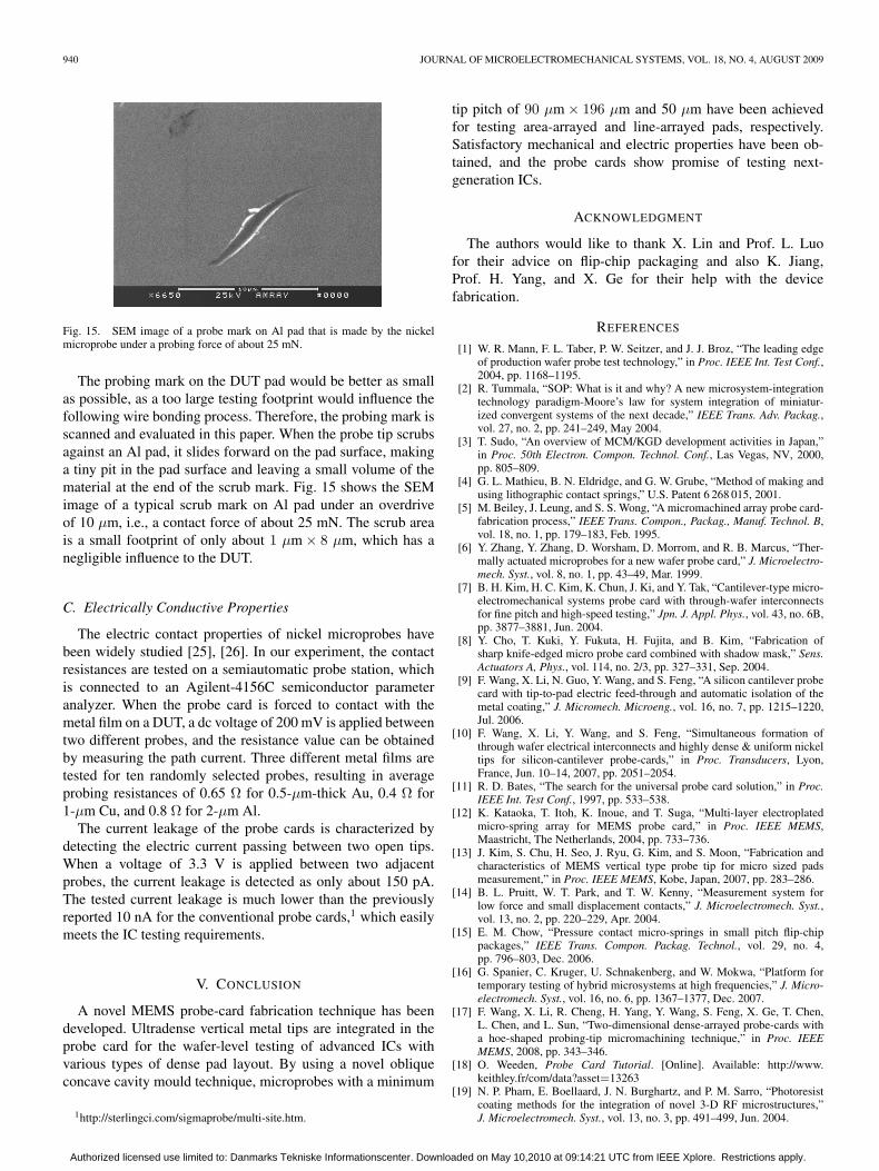
Fig. 14. (a) Schematic of the probe spring-constant testing setup. (b) Measured displacement versus contact force for the fabricated three types of probes.(c) Micrograph showing the free probe before the probing force loaded. (d) Micrograph showing the deformed probe under a force load. (e) SEM image of theworst case of the microprobes after 100 000 touchdowns, with a close-up view for the tip of this probe in (f).
A series-resistance testing scheme is designed to measure theelectrical resistance of the Sn–Ag solder bumps. The testingscheme has been described in detail in [17]. When a constantcurrent source of 20 mA is applied through the series of solderbumps, the resistance can be read by detecting the outputvoltage. The measured series resistance is never higher than1.8 Ω for 30 pairs of bumps in series, which means that theinterconnect resistance for one solder bump is generally lowerthan 0.03 Ω.
B. Mechanical Characterizations
1) Spring Constant of the Probe: The spring constant of theprobe is measured by a force–displacement tester, which is builtto measure the contact force versus tip displacement for the mi-croprobes [17]. As schematically shown in Fig. 14(a), when thepiezoelectric ceramic actuates the testing needle to contact withthe probe tip, the contact force can be monitored and read withan electric balance, while the tip displacement is in proportionto the applied voltage. In this way, the loading-displacementcurves are obtained and shown in Fig. 14(b). All the threetypes of probe cards with different spring constants havebeen tested, resulting in a good agreement with the designedresults. The difference between design and test is generally
smaller than 7%. The micrographs in Fig. 14(c) and (d) showthe microprobe before and after the loading force is applied,respectively.
When a pulsed voltage is applied to the piezoelectric ac-tuator, the testing needle would vibrate up and down. Thereliability of the probes could then be evaluated with manytouchdowns. In our experiment, the probes were able to reliablysurvive more than 100 000 repeated cycles of loading contact.Inspected with microscopy and SEM, most of the microprobesappear unchanged after the 100 000 touchdowns. However,about 5% of the probes show a little bit of wear at the tip.The SEM images shown in Fig. 14(e) and (f) are the worst caseamong the microprobes in our lifetime test and its close-up viewat the tip. Some wear is apparent for this probe.
2) Tip Planarity and Scrub Mark: The tip planarity of theprobe card is evaluated by optically scanning the probe tipsusing a WYKO NT-2000 optical metrology system (VeecoInstruments Co. Ltd.) that provides noncontact high-resolution3-D profile measurement. The testing results show that, withina 10 by 10 probe array, the nonuniformity in the tip planarityis within ±4 μm, which is better than the previously reporteddata where a cantilever-tip probe structure is used [7]. A betteruniformity could be obtained by better control of the solder-bump height variation and the bonding force during the flip-chip bonding.
Authorized licensed use limited to: Danmarks Tekniske Informationscenter. Downloaded on May 10,2010 at 09:14:21 UTC from IEEE Xplore. Restrictions apply.
940 JOURNAL OF MICROELECTROMECHANICAL SYSTEMS, VOL. 18, NO. 4, AUGUST 2009
Fig. 15. SEM image of a probe mark on Al pad that is made by the nickelmicroprobe under a probing force of about 25 mN.
The probing mark on the DUT pad would be better as smallas possible, as a too large testing footprint would influence thefollowing wire bonding process. Therefore, the probing mark isscanned and evaluated in this paper. When the probe tip scrubsagainst an Al pad, it slides forward on the pad surface, makinga tiny pit in the pad surface and leaving a small volume of thematerial at the end of the scrub mark. Fig. 15 shows the SEMimage of a typical scrub mark on Al pad under an overdriveof 10 μm, i.e., a contact force of about 25 mN. The scrub areais a small footprint of only about 1 μm × 8 μm, which has anegligible influence to the DUT.
C. Electrically Conductive Properties
The electric contact properties of nickel microprobes havebeen widely studied [25], [26]. In our experiment, the contactresistances are tested on a semiautomatic probe station, whichis connected to an Agilent-4156C semiconductor parameteranalyzer. When the probe card is forced to contact with themetal film on a DUT, a dc voltage of 200 mV is applied betweentwo different probes, and the resistance value can be obtainedby measuring the path current. Three different metal films aretested for ten randomly selected probes, resulting in averageprobing resistances of 0.65 Ω for 0.5-μm-thick Au, 0.4 Ω for1-μm Cu, and 0.8 Ω for 2-μm Al.
The current leakage of the probe cards is characterized bydetecting the electric current passing between two open tips.When a voltage of 3.3 V is applied between two adjacentprobes, the current leakage is detected as only about 150 pA.The tested current leakage is much lower than the previouslyreported 10 nA for the conventional probe cards,1 which easilymeets the IC testing requirements.
V. CONCLUSION
A novel MEMS probe-card fabrication technique has beendeveloped. Ultradense vertical metal tips are integrated in theprobe card for the wafer-level testing of advanced ICs withvarious types of dense pad layout. By using a novel obliqueconcave cavity mould technique, microprobes with a minimum
1http://sterlingci.com/sigmaprobe/multi-site.htm.
tip pitch of 90 μm × 196 μm and 50 μm have been achievedfor testing area-arrayed and line-arrayed pads, respectively.Satisfactory mechanical and electric properties have been ob-tained, and the probe cards show promise of testing next-generation ICs.
ACKNOWLEDGMENT
The authors would like to thank X. Lin and Prof. L. Luofor their advice on flip-chip packaging and also K. Jiang,Prof. H. Yang, and X. Ge for their help with the devicefabrication.
REFERENCES
[1] W. R. Mann, F. L. Taber, P. W. Seitzer, and J. J. Broz, “The leading edgeof production wafer probe test technology,” in Proc. IEEE Int. Test Conf.,2004, pp. 1168–1195.
[2] R. Tummala, “SOP: What is it and why? A new microsystem-integrationtechnology paradigm-Moore’s law for system integration of miniatur-ized convergent systems of the next decade,” IEEE Trans. Adv. Packag.,vol. 27, no. 2, pp. 241–249, May 2004.
[3] T. Sudo, “An overview of MCM/KGD development activities in Japan,”in Proc. 50th Electron. Compon. Technol. Conf., Las Vegas, NV, 2000,pp. 805–809.
[4] G. L. Mathieu, B. N. Eldridge, and G. W. Grube, “Method of making andusing lithographic contact springs,” U.S. Patent 6 268 015, 2001.
[5] M. Beiley, J. Leung, and S. S. Wong, “A micromachined array probe card-fabrication process,” IEEE Trans. Compon., Packag., Manuf. Technol. B,vol. 18, no. 1, pp. 179–183, Feb. 1995.
[6] Y. Zhang, Y. Zhang, D. Worsham, D. Morrom, and R. B. Marcus, “Ther-mally actuated microprobes for a new wafer probe card,” J. Microelectro-mech. Syst., vol. 8, no. 1, pp. 43–49, Mar. 1999.
[7] B. H. Kim, H. C. Kim, K. Chun, J. Ki, and Y. Tak, “Cantilever-type micro-electromechanical systems probe card with through-wafer interconnectsfor fine pitch and high-speed testing,” Jpn. J. Appl. Phys., vol. 43, no. 6B,pp. 3877–3881, Jun. 2004.
[8] Y. Cho, T. Kuki, Y. Fukuta, H. Fujita, and B. Kim, “Fabrication ofsharp knife-edged micro probe card combined with shadow mask,” Sens.Actuators A, Phys., vol. 114, no. 2/3, pp. 327–331, Sep. 2004.
[9] F. Wang, X. Li, N. Guo, Y. Wang, and S. Feng, “A silicon cantilever probecard with tip-to-pad electric feed-through and automatic isolation of themetal coating,” J. Micromech. Microeng., vol. 16, no. 7, pp. 1215–1220,Jul. 2006.
[10] F. Wang, X. Li, Y. Wang, and S. Feng, “Simultaneous formation ofthrough wafer electrical interconnects and highly dense & uniform nickeltips for silicon-cantilever probe-cards,” in Proc. Transducers, Lyon,France, Jun. 10–14, 2007, pp. 2051–2054.
[11] R. D. Bates, “The search for the universal probe card solution,” in Proc.IEEE Int. Test Conf., 1997, pp. 533–538.
[12] K. Kataoka, T. Itoh, K. Inoue, and T. Suga, “Multi-layer electroplatedmicro-spring array for MEMS probe card,” in Proc. IEEE MEMS,Maastricht, The Netherlands, 2004, pp. 733–736.
[13] J. Kim, S. Chu, H. Seo, J. Ryu, G. Kim, and S. Moon, “Fabrication andcharacteristics of MEMS vertical type probe tip for micro sized padsmeasurement,” in Proc. IEEE MEMS, Kobe, Japan, 2007, pp. 283–286.
[14] B. L. Pruitt, W. T. Park, and T. W. Kenny, “Measurement system forlow force and small displacement contacts,” J. Microelectromech. Syst.,vol. 13, no. 2, pp. 220–229, Apr. 2004.
[15] E. M. Chow, “Pressure contact micro-springs in small pitch flip-chippackages,” IEEE Trans. Compon. Packag. Technol., vol. 29, no. 4,pp. 796–803, Dec. 2006.
[16] G. Spanier, C. Kruger, U. Schnakenberg, and W. Mokwa, “Platform fortemporary testing of hybrid microsystems at high frequencies,” J. Micro-electromech. Syst., vol. 16, no. 6, pp. 1367–1377, Dec. 2007.
[17] F. Wang, X. Li, R. Cheng, H. Yang, Y. Wang, S. Feng, X. Ge, T. Chen,L. Chen, and L. Sun, “Two-dimensional dense-arrayed probe-cards witha hoe-shaped probing-tip micromachining technique,” in Proc. IEEEMEMS, 2008, pp. 343–346.
[18] O. Weeden, Probe Card Tutorial. [Online]. Available: http://www.keithley.fr/com/data?asset=13263
[19] N. P. Pham, E. Boellaard, J. N. Burghartz, and P. M. Sarro, “Photoresistcoating methods for the integration of novel 3-D RF microstructures,”J. Microelectromech. Syst., vol. 13, no. 3, pp. 491–499, Jun. 2004.
Authorized licensed use limited to: Danmarks Tekniske Informationscenter. Downloaded on May 10,2010 at 09:14:21 UTC from IEEE Xplore. Restrictions apply.
WANG et al.: MEMS VERTICAL PROBE CARDS WITH ULTRA DENSELY ARRAYED METAL PROBES 941
[20] X. Lin, D. Zhu, G. Xu, and L. Luo, “Lead free SnAg solder bumping withsize sub 100 microns,” in Proc. 7th ICEPT, 2006, pp. 246–250.
[21] D. R. Frear, J. W. Jang, J. K. Lin, and C. Zhang, “Pb-free solders for flip-chip interconnects,” J. Metals, vol. 53, no. 6, pp. 28–32, Jun. 2001.
[22] J. H. Lau, Flip Chip Technologies. New York: McGraw-Hill, 1996.[23] W. C. Oliver and G. M. Pharr, “An improved technique for determin-
ing hardness and elastic modulus using load and displacement sensingindentation experiments,” J. Mater. Res., vol. 7, no. 6, pp. 1564–1583,Jun. 1992.
[24] L. S. Stephens, K. W. Kelly, S. Simhadri, A. B. McCandless, andE. I. Meletis, “Mechanical property evaluation and failure analysis ofcantilevered LIGA nickel microposts,” J. Microelectromech. Syst., vol. 10,no. 3, pp. 347–359, Sep. 2001.
[25] T. Itoh, S. Kawamura, K. Kataoka, and T. Suga, “Contact propertiesof micromachined Ni probes,” in Proc. 49th IEEE Holm Conf. Electr.Contacts, Aug. 2003, pp. 223–227.
[26] K. Kataoka, T. Itoh, T. Suga, and K. Inoue, “Contact properties of Nimicro-springs for MEMS probe card,” in Proc. 50th IEEE Holm Conf.Elect. Contacts, 2004, pp. 231–235.
Fei Wang (S’06–M’09) was born in Anhui Province,China, in 1983. He received the B.S. degree in me-chanical engineering from the University of Scienceand Technology of China, Hefei, China, in 2003, andthe Ph.D. degree in microelectronics from ShanghaiInstitute of Microsystem and Information Technol-ogy, Chinese Academy of Science, Shanghai, China,in 2008.
He is currently a Postdoctoral Researcher with theDepartment of Micro- and Nanotechnology, Techni-cal University of Denmark, Lyngby, Denmark, work-
ing on micro four-point probes for IC testing. His research interests includeMEMS fabrication and design, IC device testing, and contact phenomena inelectronic measurement.
Rong Cheng received the B.Sc. degree in micro-electronics from Fudan University, Shanghai, China,in 2006. She is currently working toward the Ph.D.degree in microelectronics in the State Key Labora-tory of Transducer Technology, Shanghai Institute ofMicrosystem and Information Technology, ChineseAcademy of Sciences, Shanghai, China.
Her current research interests include design andfabrication of integrated MEMS probe cards forwafer-level IC testing.
Xinxin Li was born in Liaoning Province, China, in1965. He received the B.S. degree in semiconduc-tor physics and devices from Tsinghua University,Beijing, China, in 1987, and the M.S. and Ph.D.degrees in microelectronics from Fudan University,Shanghai, China, in 1995 and 1998, respectively.
He was a Research Engineer with Shenyang In-stitute of Instrumentation Technology for five years.He was also with Hong Kong University of Scienceand Technology, Kowloon, Hong Kong, as a Re-search Associate, and with Nanyang Technological
University, Singapore, as a Research Fellow. He then joined Tohoku University,Sendai, Japan, as a nonpermanent Lecturer (COE Research Fellowship). Since2001, he has been a Professor at the Shanghai Institute of Microsystem andInformation Technology, Chinese Academy of Sciences, Shanghai, where hecurrently serves as the Director of the State Key Laboratory of TransducerTechnology. He is also currently an Adjunct Professor with both FudanUniversity and Shanghai Jiaotong University, Shanghai. For a long period oftime, his research interests have been in the fields of micro/nanosensors andtransducers, micro/nanoelectromechanical systems (MEMS/NEMS), and mi-cro/nanoelectromechanical integration technologies. He is an Editorial Boardmember of the Journal of Micromechanics and Microengineering and theInternational Journal of Information Acquisition. He has authored about40 patents and published about 200 papers in refereed journals and conferenceproceedings.
Dr. Li served as the TPC member for 2008 IEEE International Conference onMicro Electro Mechanical Systems (IEEE MEMS-08), for IEEE InternationalConference on Sensors (IEEE Sensors) from 2002 to 2008 and for Transduc-ers’09. He is the editorial board member for Journal of Micromechanics andMicroengineering and International Journal of Information Acquisition. Heserved as a Technical Program Committee member for the 2008 IEEE Inter-national Conference on Micro Electro Mechanical Systems (IEEE MEMS-08),for the IEEE International Conference on Sensors (IEEE Sensors) from 2002 to2008, and for Transducers’09.
Authorized licensed use limited to: Danmarks Tekniske Informationscenter. Downloaded on May 10,2010 at 09:14:21 UTC from IEEE Xplore. Restrictions apply.