mems reliability assurance guidelines for space applications · 2015-07-29 · mems reliability...
TRANSCRIPT
JPL Publication 99-1
MEMS Reliability Assurance Guidelinesfor Space Applications
Brian StarkEditorJet Propulsion Laboratory, Pasadena, California
National Aeronautics andSpace Administration
Jet Propulsion LaboratoryCalifornia Institute of TechnologyPasadena, California
January 1999

ii
The research described in this publication was carried out by the Jet Propulsion Laboratory,California Institute of Technology, under a contract with the National Aeronautics and SpaceAdministration.
Reference herein to any specific commercial product, process, or service by trade name,trademark, manufacturer, or otherwise, does not constitute or imply its endorsement by theUnited States Government or the Jet Propulsion Laboratory, California Institute of Technology.
iii
Preface
This guideline was developed as an aid to help in the understanding ofMicroelectromechanical Systems (MEMS) reliability and to facilitate the insertion of thistechnology into high reliability applications. Modeled after the GaAs MMIC ReliabilityAssurance Guideline for Space Applications by Kayali et al., it was felt that a guideline wouldbe more advantageous to people than a strict specification. With the MEMS industry as diverseas it is today, it seemed presumptuous to lay out specific tests for every MEMS device insertedinto space as that kind of document would be unduly constrictive to some applications. Ratherthis document was intended as a MEMS educational guide, offering descriptions of the mostcommon devices and technologies and the steps required to meet the demands of the spaceenvironment.
The focus of this guide is upon methods rather than tests and as such, it is assumed thatthe ultimate responsibility for reliability lies in the hands of the user. Ultimately it is felt that thedesigners and the customers will have to reach an understanding as to the exact qualificationneeds of a particular device.
The guideline begins with a chapter on the recent developments in the field of MEMSand the need for an understanding of related reliability issues. Chapter 2 offers a basic reviewof reliability models and of semiconductor failure distributions. This chapter is intended to aidthe reader in understanding the meaning of reliability tests in general, and how they may apply toMEMS.
Chapter 3 describes the known failure mechanisms that have been characterized inMEMS technology. While the bulk of the chapter is dedicated to mechanical fracture, it mustbe understood that each failure mechanism will have a different level of predominance ondifferent devices. Chapter 4 describes the basic material properties of common MEMSmaterials and relates these to the theory presented in Chapter 3.
Chapter 5 provides a description of common MEMS processing techniques. Both thediscrete steps used to make the devices and the combination of those steps into a coherentprocess are discussed. A description of common MEMS device elements is presented inChapter 6, along with relevant reliability concerns.
Chapter 7 discusses methods for modeling structure using finite element analysis.Chapter 8 involves reliability issues in packaging. Chapter 9 describes common test structuresused to characterize the materials properties and structures discussed in Chapters 3 and 6.

iv
Finally Chapter 10 offers a summary of the ways to use the information from theprevious chapters to develop a reliable, space qualified, MEMS device. The information in thisdocument is only a compilation of much deeper works and it is felt that users of this guidelineshould reference other documents listed throughout this guideline in the process of furtheringMEMS reliability.
I would also like to thank the people involved in the production of this document.Sammy Kayali provided both technical advice and moral support throughout the arduousprocess of writing this guideline. Joseph Bernstein helped in the organization of the guidelineand helped me to understand the material in Chapter 2. Bill Tang of the Micro DevicesLaboratory at JPL gave great help in the processing area and lent his general expertise toimproving the quality of the guideline. Dave Gerke, the resident packaging expert at JPL, wasinstrumental in producing the material on packaging issues in MEMS. Jim Newell and Kin Manin the Engineering Technology section at JPL provided invaluable modeling and dynamic testingmaterial for the guideline. Finally, Thomas Kenny proofread the document and providedvaluable feedback in the editing phase.
I would also like to acknowledge those people that did not contribute to the documentitself, but who helped to make it possible through their encouragement. Russell Lawton, as thePI for MEMS Reliability at JPL, procured the funding for this document and acquired many ofthe images contained herein. Noel MacDonald, an electrical engineering professor at Cornell,provided the academic encouragement to enter into this emerging field and, without his teaching,this document would never have been produced. Norman Tien, also an electrical engineeringprofessor at Cornell, helped by explaining some complicated issues in the field of surfacemicromachining. Rishi Khanna, Valdis Rigdon, and Dipak Srinivasan, also of Cornell, providedthe incentive to start writing this document back in December of 1996. Greg Radighieri ofTexas A&M also helped through his input and valuable insight into mechanical engineeringissues.
Brian StarkAugust 1998

v
Abstract
This guide is a reference for understanding the various aspects ofmicroelectromechanical systems, or MEMS, with an emphasis on device reliability. Materialproperties, failure mechanisms, processing techniques, device structures, and packagingtechniques common to MEMS are addressed in detail. Design and qualification methodologiesprovide the reader with the means to develop suitable qualification plans for the insertion ofMEMS into the space environment.

vi
Contributors
Joseph Bernstein University of Maryland
David Gerke Jet Propulsion Laboratory
Sammy Kayali Jet Propulsion Laboratory
Thomas Kenny Stanford University
Kin Man Jet Propulsion Laboratory
James Newell Jet Propulsion Laboratory
William Tang Jet Propulsion Laboratory
vii
Table of Contents
Chapter 1: Introduction 1B. Stark and W. C. Tang
I. A Brief Description of MEMS 1II. The Potential of MEMS 1III. Current MEMS Technologies 3IV. The Need for, and Role of, MEMS Reliability 4V. Additional Reading 5
Chapter 2: Reliability Overview 7B. Stark and J. Bernstein
I. Reliability Measures 8A. Probability Density Function 8B. Failure Rate 8C. The Bathtub Curve 9D. Predicting Time to Failure 10E. Failure Rate Units 11
II. Probability Models 11A. The Uniform Distribution 11B. The Weibull Distribution 12C. The Normal Distribution 14D. The Lognormal Distribution 15
III. Application of Reliability Models 16IV. Failure 18V. Additional Reading 19
Chapter 3: Failure Modes and Mechanisms 21B. Stark
I. Mechanical Fracture 21A. Definitions 21B. Stress-Induced Failure 26C. Point Defects 28
i) Vacancies 28ii) Interstitial 29iii) Point Replacement 29
D. Dislocations 29i) Edge Dislocation 30ii) Screw Dislocation 30
E. Precipitates 31
viii
F. Fracture Strength 32G. Fatigue 34
II. Stiction 35III. Wear 36IV. Delamination 38V. Environmentally Induced Failure Mechanisms 39
A. Vibration 39B. Shock 39C. Humidity Effects 39D. Radiation Effects 40E. Particulates 41F. Temperature Changes 41G. Electrostatic Discharge 42
VI. Stray Stresses 42VII. Parasitic Capacitance 43VIII. Dampening Effects 44IX. Additional Reading 47
Chapter 4: Material Properties 49B. Stark
I. Single Crystal Silicon 49II. Polycrystalline Silicon 53III. Silicon Dioxide 55IV. Silicon Carbide 56V. Silicon Nitride 57VI. Gallium Arsenide 59VII. Metals 63
A. Aluminum 64B. Gold 65C. Copper 65
VIII. Polyimides 66IX. Additional Reading 67
Chapter 5: MEMS Device Processing 69B. Stark and W. C. Tang
I. Microfabrication Processing Steps 69A. Thin Film Growth and Deposition 69
i) Spin Casting 69ii) Evaporation 70iii) Sputtering 71iv) Reactive Growth 72
ix
v) Chemical Vapor Deposition 73vi) Plasma Deposition 74
B. Photolithography 75i) Mask Fabrication 75ii) Alignment and Exposure 76
C. Etching and Patterning Techniques 76i) Lift-off 76ii) Wet Etching 76iii) Dry Etching 77
II. MEMS Fabrication Processes 78A. Bulk Micromachining 78
i) Bulk Micromachining with a Wet Etch 79ii) Bulk Micromachining with a Dry Etch 80iii) Wafer Bonding 81iv) Reliability Issues 82
B. Surface Micromachining 83i) Reliability Issues 85
C. LIGA 86i) Reliability Issues 88
D. GaAs Processing 88i) Reliability Issues 90
III. Additional Reading 90
Chapter 6: Common Device Elements 91B. Stark
I. Structural Beams 92A. Structural Analysis of Support Beams 93
i) Static Deflections 93ii) Oscillatory Motion 97
B. Failure of Structural Beams 99C. Additional Reading 102
II. Thin Membranes 103A. Structural Analysis of Membranes 103
i) Static Deflection 103ii) Lamb Waves 105iii) Modal Waves 108
B. Failure of Membranes 109C. Additional Reading 111
III. Hinges 112A. Structural Analysis 113B. Reliability Concerns 114
x
C. Additional Reading 114IV. Piezoresistive Transducers 115
A. Formal Definition 115B. Piezoresistive Sensors 116C. Reliability Issues 118D. Additional Reading 119
V. Tunneling Tips 120A. Physical Description 122B. Reliability Concerns 123C. Additional Reading 124
VI. Electrostatic Actuators and Transducers 125A. Parallel Plate Capacitors 125
i) Electrical and Mechanical Analysis 126ii) Limitations of Parallel Plate Capacitors 128iii) Additional Reading 128
B. Comb Drives 129i) Mechanical and Electrical Analysis 129ii) Limitations on Design 130iii) Additional Reading 134
C. Micromotors 135i) Electrostatic Motor Analysis 135ii) Harmonic Motors 136iii) Microbearing Reliability Concerns 137iv) Additional Reading 138
VII. Magnetic Actuators 139A. Mechanical and Electrical Analysis 141B. Reliability Concerns 142C. Additional Reading 143
VIII. Thermal Actuators 144A. Bimetallic Strips 144B. Mechanical Analysis 144C. Shape Memory Alloys 146D. Reliability Issues for Thermal Actuators 147E. Additional Reading 148
IX. Piezoelectric Actuators 149A. The Piezoelectric Effect 149B. Piezoelectric Devices 150C. Reliability Issues 150D. Additional Reading 151
Chapter 7: Finite Element Analysis and Applications to MEMS 152

xi
J. Newell, K. Man, and B. StarkI. Heat Transfer Analysis 153II. Thermal Stress Analysis 155III. Thermal Fatigue Stress Analysis 156IV. Static Analysis 159V. Modal Analysis 161VI. Software Tools 162VII. Additional Reading 164
xii
Chapter 8: MEMS Packaging 166R. D. Gerke
I. Introduction 166II. Functions of MEMS Packages 166
A. Mechanical Support 167B. Protection From Environment 167C. Electrical Connection to Other System Components 168D. Thermal Considerations 168
III. Types of MEMS Packages 170A. Metal Packages 170B. Ceramic Packages 171C. Thin-Film Multilayer Packages 172D. Plastic Packages 172
IV. Package-to-MEMS Attachment 173V. Chip Scale Packaging 175
A. Flip Chip 175B. Ball-Grid-Array (BGA) 180
i) Ceramic Ball-Grid-Array (CBGA) 180ii) Plastic Ball-Grid-Array (PBGA) 181iii) Micro-Ball-Grid-Array (µBGA) 181
VI. Multichip Packaging 182A. MCM/HDI 182
i) COF/HDI Technology 182ii) MEMS Test Chip 184
B. System on a Chip (SOAC) 186VII. Plastic Packaging (PEMs) 186VIII. Additional Reading 190
Chapter 9: Test Structures 193B. Stark
I. Technology Characterization Vehicle 193II. Standard Evaluation Devices 193III. Parametric Monitors 194
A. Beam Stubs 194B. Elastic Measurements 195
i) Bending Beam Method 195ii) Resonant Beam Structures 196
C. Stress/Strain Gauges 197i) Bent Beam Strain Sensors 197ii) Cantilever Beams 199iii) Buckling Beam Structures 200
xiii
iv) Substrate Analysis 201D. Undercut Squares 202
IV. Fracture Specimens 202A. Thermal Properties Measurements 203
i) Cantilever Beam Method 203ii) Thin Film Heater 203iii) Microbridge 204
V. Additional Reading 205
Chapter 10: Qualification Testing Protocols for MEMS 207B. Stark and S. Kayali
I. Process Qualification 210A. Process Step Development 213B. Wafer Fabrication Documentation 215C. Parametric Monitors 215D. Design-Rule and Model Development 215E. Wafer Level Tests 216F. TCV and SED Tests 216G. Starting Materials Control 216H. Electrostatic Discharge Characterization and Sensitivity 217
II. Product Qualification 217A. MEMS Design and Layout Verification 218B. Electromechanical Performance Verification 218C. Thermal Analysis 218D. ESD Sensitivity Tests 219E. Voltage Ramp 219F. Temperature Ramp 219
III. Product Acceptance 219A. SEM Analysis 224B. Nondestructive Bond Pull Test 225C. Visual Inspection 225D. Laser Profile 225E. IR Scan 225F. Mechanical Shock Screen 226G. Constant Acceleration 226H. Temperature Cycling and Shock Screen 226I. Particle Impact Noise Detection 227J. Burn-In 227K. Leak Test 227L. Radiographic 228
IV. Company Certification 228

xiv
A. Technology Review Board 230B. Conversion of Customer Requirements 231C. Manufacturing Control Procedures 232D. Equipment Calibration and Maintenance 232E. Training Programs 233F. Corrective Action Program 233G. Self-Audit Program 233H. Electrostatic Discharge Handling Program 234I. Cleanliness and Atmospheric Controls 234J. Record Retention 234K. Inventory Control 235L. Statistical Process Control 236
V. Additional Reading 236
Appendix: Mission Specific Environmental Testing 237J. Newell and K. ManA. Test Procedures 237
i) Test Sequencing 238B. Environmental Test Requirements 239
i) Launch Environment 240ii) Thermal 240iii) Definitions 240iv) Thermal Radiation 241v) Vacuum Pressure Decay 241vi) Dynamics 242
References 267
About the Authors 283

xv
xvi
List of Figures and Tables
Figure 1-1: A partially packaged microgyroscope developed at JPL................................. 2
Figure 2-1: The Bathtub curve....................................................................................... 10
Figure 2-2: Probability of survival to time t..................................................................... 11
Figure 2-3: The pdf of the Weibull function with different b values .................................. 12
Figure 2-4: pdf of the normal distribution....................................................................... 14
Figure 2-5: pdf of the lognormal distribution................................................................... 15
Figure 2-6: An example of using the lognormal distribution to predict lifetime in ICs.......... 16
Figure 3-1: Generalized stress states on a 3-D unit cube................................................. 22
Figure 3-2: Young's modulus as a function of crystalline orientation for Si and GaAs alongthe <100> axis............................................................................................ 23
Figure 3-3: Euler's angles .............................................................................................. 24
Figure 3-4: Poisson's ratio as a function of angle in the (100) plane with 1 and m varying inthe (100) plane............................................................................................ 25
Figure 3-5: Stress versus strain relationships for bulk Si and GaAs ................................. 26
Figure 3-6: Stress concentration factor as a function of geometry for thin beams ............. 27
Figure 3-7: Different point defects ................................................................................. 28
Figure 3-8a: Edge dislocation.......................................................................................... 29
Figure 3-8b: Screw dislocation........................................................................................ 29
Figure 3-9: Representative plot of the probability of the fracture of silicon under applied stress................................................................................................................... 33
Figure 3-10: Typical SN curve for a ductile material......................................................... 34
Table 3-1: Fatigue induced materials degradations ........................................................ 35
Figure 3-11: Polysilicon cantilever adhering to substrate................................................... 36
xvii
Table 3-2: Wear coefficients for nonmetals ................................................................... 37
Figure 3-12(a,b): Cracks in single crystal silicon support beams caused by vibrations from alaunch test................................................................................................... 39
Figure 3-13: Diagram of parasitic capacitance between silicon base and metallization layer ona bulk micromachined beam........................................................................ 44
Figure 3-14: Definition of resonance and Q...................................................................... 45
Figure 3-15(a,b): The difference in amplitude between a linear resonator operating in resonanceand operating at a non-resonant frequency................................................... 46
Table 4-1: Room-temperature properties of single crystal silicon................................... 50
Figure 4-1: Crystal structure of silicon............................................................................ 51
Figure 4-2: Energy band structures of Si and GaAs........................................................ 52
Figure 4-3: Residual stress as a function of deposition conditions.................................... 53
Table 4-2: Room temperature properties of silicon dioxide............................................ 55
Table 4-3: Dominant SiC types .................................................................................... 56
Table 4-4: Room temperature properties of SiC ........................................................... 56
Table 4-5: Room temperature properties of silicon nitride.............................................. 57
Figure 4-4: Residual stress in silicon nitride films as a function of processing conditions.... 58
Figure 4-5: Crystalline gallium arsenide.......................................................................... 59
Table 4-6: Room temperature properties of gallium arsenide ......................................... 60
Table 4-7: Room temperature properties of AlAs ......................................................... 61
Figure 4-6: Stress versus strain curve for a ductile material............................................. 63
Table 4-8: Room temperature properties of 99.6% pure aluminum................................ 64
Table 4-9: Properties of gold........................................................................................ 65
Table 4-10 : Properties of 99.99% copper ...................................................................... 66

xviii
Table 4-11: Properties of PMDA/BPDA/TFMOB polyimide.......................................... 67
Figure 5-1: A typical evaporation system....................................................................... 70
Figure 5-2: Basic sputtering system................................................................................ 71
Figure 5-3: Reactive growth process ............................................................................. 72
Figure 5-4: A chemical vapor deposition system............................................................ 73
Figure 5-5: The basic photolithographic process in a cross sectional view....................... 74
Figure 5-6: Typical alignment machine ........................................................................... 75
Figure 5-7: A side view of a generic bulk micromachining process.................................. 79
Figure 5-8: A side view of one of the dry etch micromachining processes ....................... 80
Figure 5-9: Hillocks caused by wet etchants .................................................................. 82
Figure 5-10: Possible sidewall features created by a poorly controlled RIE....................... 83
Figure 5-11: The surface micromachining process using three layers of polysilicon............. 84
Figure 5-12: MEMS structure with a large residual stress................................................. 85
Figure 5-13: The basic LIGA process ............................................................................. 87
Figure 5-14: Fabrication of a suspended structure in GaAs............................................... 89
Figure 5-15: Fabrication of an AlGaAs membrane ........................................................... 90
Figure 6-1: Cross section of common MEMS beams..................................................... 92
Figure 6-2: SEM picture of beam with all dimensions labeled ......................................... 92
Figure 6-3: Displacement of loaded cantilever beams ..................................................... 94
Figure 6-4: Graphical representation of a cantilever beam deforming under a transverse load................................................................................................................... 95
Figure 6-5: Beams displacing an angle, φ, due to an applied torque ................................ 96
Table 6-1: Constants for rectangular cross sections under a torsional load ..................... 97
xix
Figure 6-6: Oscillatory modes for cantilever beams and built-in beams............................ 99
Figure 6-7: Side and cross sectional views of cantilever beam under shear force andbending movement .................................................................................... 101
Figure 6-8: A thin plate viewed at 200x magnification................................................... 103
Figure 6-9a: Dependence of C1 and C2 upon Poisson's ratio.......................................... 105
Figure 6-9b: w1/w0 and w1/w0 as a function of Poisson's ratio......................................... 105
Figure 6-10: Wave propagation in solid media ............................................................... 106
Figure 6-11: First six vibratory modes and resonant frequencies in a square plate with nodallines shown .............................................................................................. 109
Table 6-2: Plate coefficients (four sides fixed)............................................................. 111
Figure 6-12: A typical hinge .......................................................................................... 112
Figure 6-13 (a-c): Three basic hinges as presented by Pister et al. ..................................... 113
Figure 6-14 (a,b): Schematic representation of the position of four piezoresistors on amembrane and accompanying circuit diagram............................................. 118
Figure 6-15: P(N,T) for n silicon ................................................................................... 119
Figure 6-16: Probability distribution of an electron trapped in a well ............................... 121
Figure 6-17: Tunneling tip on SCS beams...................................................................... 121
Figure 6-18: Typical layout for a tunneling sensor........................................................... 123
Figure 6-19: Closeup view of parallel plate capacitor with the area and gap labeled........ 125
Figure 6-20: Basic circuit for detecting changes in capacitance ....................................... 127
Figure 6-21: A standard comb drive.............................................................................. 129
Figure 6-22: Overhead view of basic unit of a comb drive.............................................. 130
Figure 6-23: Overhead view of comb drive structure with spring constants and dimensionslabeled...................................................................................................... 131
xx
Figure 6-24: An example of the damage that results when two comb drive electrodes comeinto contact and short out the device.......................................................... 132
Figure 6-25: Electrostatically driven micromotor ............................................................ 134
Figure 6-26: A basic harmonic motor layout .................................................................. 137
Figure 6-27: A magnetic actuator designed by Judy et al. .............................................. 139
Figure 6-28: Diagram of forces acting on soft magnetic plate.......................................... 140
Figure 6-29: Side view of two metallic strips bending due to temperature stress.............. 143
Table 6-3: Properties of nitinol at different temperatures.............................................. 146
Figure 6-30: Mechanical response as a function of frequency for a thermal actuator ....... 147
Figure 6-31: Diagram of a piezoelectric transducer ........................................................ 149
Figure 7-1: Hybrid device with cover removed ............................................................ 152
Figure 7-2: Substrate mounted die............................................................................... 153
Figure 7-3: Channel barrier schematic.......................................................................... 153
Figure 7-4: Temperature distribution in channel barrier................................................. 154
Figure 7-5: Finite element model of a vaporizing liquid microthruster............................. 156
Figure 7-6: Electron micrograph of 3-D intermetallic via............................................... 156
Figure 7-7: Inter-metallization via geometry.................................................................. 157
Figure 7-8: Finite element model of intermetallic via...................................................... 157
Figure 7-9: Stress-strain hysteresis loop from finite element analysis.............................. 158
Figure 7-10: Static deflection of a 3 µm thick Si membrane subjected to a 1 MPa pressure................................................................................................................. 159
Figure: 7-11: Finite element model of a micromagnetometer............................................ 160
Figure: 7-12: 1st resonant mode..................................................................................... 161
Figure 7-13: 2nd resonant mode.................................................................................... 161
xxi
Table 7-1: Finite element modeling software packages................................................ 163
Figure 8-1: Cross section of MMIC attached to a package and its equivalent thermal circuit................................................................................................................. 169
Figure 8-2: MEMS device in compression................................................................... 173
Figure 8-3: Schematic representation of silver filled epoxy resin.................................... 174
Figure 8-4: C4 (Controlled Collapse Chip Connection) flip chip................................... 175
Figure 8-5: Mechanical and electrical connections........................................................ 175
Figure 8-6: Interconnect density (wire bond vs. C4)..................................................... 177
Table 8-1 Summary of reliability test conditions and results for fluxless flip-chipthermocompression-bonded bump contacs ................................................ 178
Figure 8-7: Ceramic Ball-Grid-Array Package shown with connections on 50 mil centersillustrating the high number of connections .................................................. 179
Figure 8-8: A schematic representation of a Plastic Ball-Grid-Array Package ............... 180
Figure 8-9: Chip-on-Flex (COF) process flow............................................................ 182
Figure 8-10: Large area ablation for MEMS access in COF package............................. 182
Table 8-2: MUMPs layer thickness............................................................................ 183
Figure 8-11: Cross-section of MUMPs layout ............................................................... 183
Table 8-3: MEMS device categories included on surface micromachining test die ........ 184
Table 8-4: MEMS device categories included on bulk micromachining test die ............ 184
Figure 8-12: Windows laser ablated in COF overly for MEMS access........................... 185
Figure 8-13: Typical plastic package showing the onset of a crack ................................. 186
Figure 8-14: Mold compound properties ....................................................................... 186
Figure 8-15: Moisture weight gain of a plastic package exposed to two different moistureconditions ................................................................................................. 187
xxii
Figure 8-16: Polyimide die overcoat (PIX) on MEMS die: top surface only, on packageframe, and on package frame and sides only .............................................. 187
Figure 8-17: Typical geometry of wire bond with different die settings: raised, downset,double downset......................................................................................... 188
Figure 9-1: A row of beam stubs................................................................................. 194
Figure 9-2: Bending beam method............................................................................... 195
Figure 9-3: Resonant beam array................................................................................. 196
Figure 9-4: Layout of comb-drive resonator ................................................................ 197
Figure 9-5: Stress/strain gauge..................................................................................... 198
Figure 9-6: Tensile tester reported by Tsuchiya et al..................................................... 202
Figure 9-7: Tensile tester reported by Greek et al. ....................................................... 203
Figure 9-8: Layout of thin film heater with thermocouples ............................................ 204
Figure 9-9: Layout of a microbridge ........................................................................... 205
Figure 10-1: Reliability over the development cycle........................................................ 206
Figure 10-2: Recommended qualification methodology................................................... 207
Figure 10-3: MEMS process qualification steps............................................................. 211
Figure 10-4: MEMS process reliability evaluation.......................................................... 212
Figure 10-5: Device design validation............................................................................ 212
Figure 10-6: MEMS part qualification overview............................................................. 221
Figure 10-7: Lot acceptance test for die ........................................................................ 220
Figure 10-8: Wafer acceptance test............................................................................... 223
Table 10-1: Typical packaged device screening............................................................ 224
Figure 10-9: Reliability audit.......................................................................................... 227
Table A-1: Thermal radiation levels ............................................................................. 241
xxiii
Figure A-1: Launch pressure decay rate ....................................................................... 242
Table A-2: Quasi-static accelerations .......................................................................... 243
Figure A-2(a-e): Device design validation......................................................................... 242
Table A-3: Sinusoidal vibration................................................................................... 247
Figure A-3: Vibration levels transmitted to flight article through mounts.......................... 248
Figure A-4: Payload/flight article response to vibroacoustic environment........................ 249
Figure A-5: Minimum vibration levels for workmanship defect detection........................ 249
Figure A-6: Composite random vibration envelope....................................................... 250
Table A-4: Random vibration specifications................................................................. 251
Figure A-7: Typical acoustic noise requirement............................................................. 252
Table A-5: Acoustic specification table........................................................................ 253
Table A-6: Calculation of overall sound pressure level ................................................. 254
Figure A-8: Envelope of acoustic flight data.................................................................. 255
Table A-7: Acoustic test problem/failure history........................................................... 257
Table A-8: Control parameter sensitivity and cost........................................................ 257
Table A-9: Acoustic noise spectra............................................................................... 259
Figure A-9: Typical pyrotechnic shock requirement ...................................................... 260
Figure A-10: Subassembly pyrotechnic shock design requirement ................................... 261
Figure A-11: Pyro shock acceleration time history.......................................................... 262
Figure A-12: Frequency response to pyro shock............................................................ 260
Figure A-13: Response spectrum in resonant plate test ................................................... 264
Figure A-14: Mechanical impulse pyro shock simulator................................................... 265
Table A-10: Control parameter sensitivity and cost........................................................ 266

xxiv
Table A-11: Shock response spectrum (Q=10)............................................................. 264
Figure A-15: Shock spectrum........................................................................................ 265
1
Chapter 1: Introduction
B. Stark and W. C. Tang
This chapter offers a brief description of the MEMS industry as it stands today.Assuming no familiarity with the subject matter, it explains the basic concepts behind MEMSand how they are being applied to meet current technological challenges in different markets.This chapter also describes the basic methodology that will be applied throughout this booktowards qualifying a high-reliability MEMS device.
I. A Brief Description of MEMS
MEMS is an acronym that stands for microelectromechanical systems. It is a broadterm that encompasses a fairly nebulous group of products. Essentially, MEMS are anyproduct, ranging in size from a micron to a centimeter, that combines mechanical and electricalstructures. Although the possible scope of MEMS is fairly limitless, for the sake of conventionsand the need for brevity, this book will only address the more common MEMS technologies.
Initially MEMS developed from technologies used in the semiconductor industry for theproduction of electronic circuits. Less than 10 years after the invention of the integrated circuit,H. C. Nathanson used microelectronic fabrication techniques to make the world's firstmicromechanical device.[2] By the early 1980s, due to massive improvements in processingtechnologies, micromechanical devices grew in popularity. In the ensuing years, a new industrywas born, where electromechanical systems could be realized on micrometer scales. The resultwas a whole new class of sensors and actuators that performed common tasks on smaller scalesthat were ideally suited for mass production.
MEMS, in its most conventional sense, refers to a class of batch-fabricated devicesthat utilize both mechanical and electrical components to simulate macroscopic devices on amicroscopic scale. This guideline focuses upon the conventional definition of MEMS. Theessence of MEMS is that they are small devices that perform mechanical tasks in ways and,more importantly, in quantities that conventional devices cannot.
II. The Potential of MEMS
In the wake of the explosion of the microprocessor in the early eighties, thesemiconductor industry revealed its immutable law that smaller is better. With economies ofscale turning tiny firms into industrial behemoths, it became evident that mass miniaturization,along with mass distribution, could produce huge revenues and substantively change the daily
2
lives of average citizens. Given the unmitigated success of the microcircuit, it became only amatter of time before technologies would emerge that could bring machines to the microscopicworld and produce similar results. With MEMS poised to do for machines what the transistordid for computers, there has been a vast explosion of interest, and thus funding, in MEMSresearch.
MEMS are used to perform the tasks of macroscopic devices at a fraction of the costand with, occasionally, improved functionality and performance. By using simple mechanicalstructures and tailoring integrated circuits to suit specific tasks, designers have seen a drasticreduction in device scales and the implementations of functions that were previously unrealized.Their size alone makes them attractive for limited mass applications, with the automotive,biomedical, communications, data storage, and aerospace industries taking a keen interest inMEMS developments. Far more promising, though, is the possible reduction in costs offeredby MEMS. By combining increasing throughput with fixed cost structures, manufacturers canlinearly reduce prices by a comparable production increase. Offering economies unique to thesemiconductor industry, MEMS have the potential to revolutionize the industrial age.
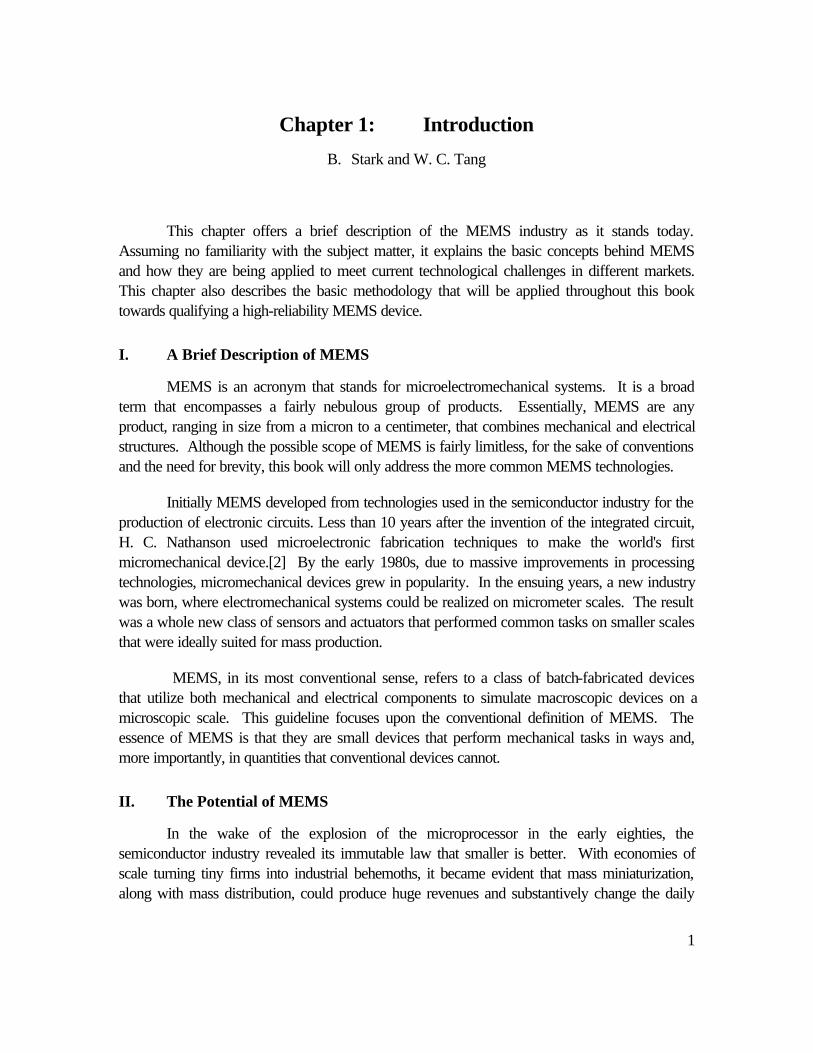
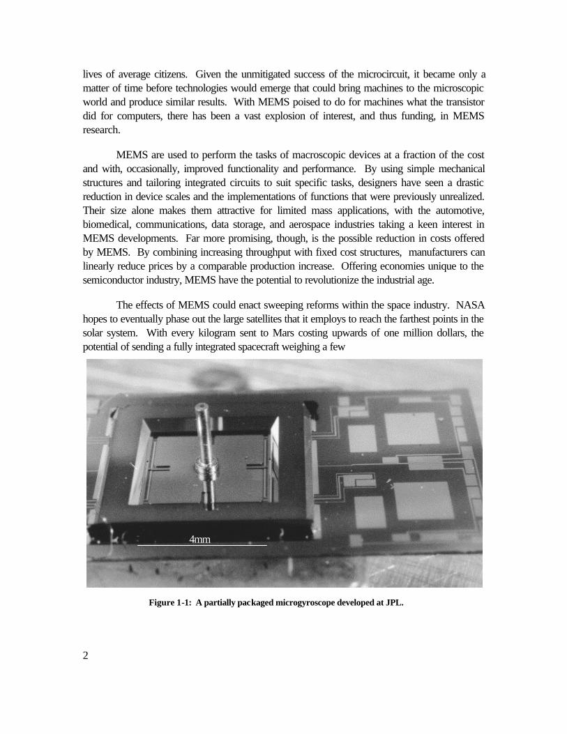
The effects of MEMS could enact sweeping reforms within the space industry. NASAhopes to eventually phase out the large satellites that it employs to reach the farthest points in thesolar system. With every kilogram sent to Mars costing upwards of one million dollars, thepotential of sending a fully integrated spacecraft weighing a few
Figure 1-1: A partially packaged microgyroscope developed at JPL.
4mm
3
kilograms instead of the thousands of kilos offers significant monetary benefits. With MEMScapable of performing certain functions of macroscopic devices, the benefit of cutting the cost ofresearch missions cannot be understated given this era of shrinking budgets. Space applicationsof MEMS are only a small part of their full potential. MEMS are also capable of revolutionizingthe information age by changing the daily fabric of our terrestrial existence.
III. Current MEMS Technologies
Understanding the stated advantages of MEMS, designers have started developing arange of products to suit their needs. The first major MEMS to hit markets were pressuresensors for engine control in cars. This development was followed by the introduction ofmicroaccelerometers, which were pioneered to provide zero-fault air bag deployment systems.Integrating a diagnostic circuit into a sensor, engineers were able to produce a device that couldnot only sense acceleration but that could also detect internal failures. Replacing a faulty systembased on ball bearings and plastic tubing that was prone to misfire, these devices swept throughthe automotive industry. Building from the technological, as well as commercial, success ofthese initial designs, engineers have developed MEMS to act as a wide variety of motionsensors. Recently intense research has been conducted into producing microgyroscopes as partof a fully integrated inertial reference unit. Development has also commenced, seismometers,anemometers, temperature sensors, pressure sensors, and hygrometers which, whenincorporated with accelerometers, could provide miniaturized weather stations.
MEMS have also shown promise for aerospace applications. Research intomagnetometers shows that it may be possible to build devices that far outperform traditionalsolid-state sensors, which could provide cost saving reductions in the weight of spacecraft.Furthermore, the bulky propulsion systems in modern satellites will be phased out by advancesin micropropulsion coming from new generations of ion drives and microthrusters. Recentdevelopments at universities have shown that MEMS microactuators, when placed upon theleading edge of aircraft, can offer significant drag reduction and thus increase fuelefficiency.[182] Some even more interesting research has led to the design of a MEMScontrolled aircraft, where control surfaces are replaced by micromachines, which could offerunprecedented control and diagnostic capabilities.
One of the more promising fields within MEMS is the concept of optical MEMS. Usingmicromirrors placed on top of memory arrays, researchers have developed a televisionprojection unit on a semiconductor wafer that has all the functionality of a cathode ray tube.[3]Another promising development is in the field of optical switches. Conventional opticalswitching networks are costly and, with the forecasted growth in optical communicationssystems, cheaper alternatives are at a premium. Multiple groups have developed MEMS-basedoptical switches that can be produced at a fraction of the cost of conventional systems.
4
With the digital age largely upon the American public, MEMS are poised to offergreater improvements in computer technology. Given that power dissipation of the averagemicroprocessor increases with every generation of microchip, microtubules research has beeninitiated to attempt to find better ways to conduct heat away from integrated circuits. MEMSstructures have also been developed as microprobes for integrated circuits.[10] Using MEMS,it may be possible to take point contact voltage and current measurements on microprocessors.Another exciting development has been the pioneering of nanometer scale data storage. Withminiaturized tunneling tips now possible, engineers have developed systems that could eventuallystore information at commercially competitive speeds in an area twenty nanometers on a side.
Another field that shows promise is the development of biological sensors. MEMSprovides an opportunity for the development of new sensors to monitor the human environment.Researchers at JPL have begun to develop MEMS-based pills that can provide informationabout the digestive system. Another interesting application of MEMS has been in thedevelopment of new biological instruments. Researchers have, among other developments,produced probes to measure the strength of the human heart cell.[183]
While the potentials of MEMS are almost limitless, production of commercial parts hasbeen heretofore limited. MEMS, as products of a young industry, remain largely prototypical.While their potential have been demonstrated their actual implementation has been relativelyscarce, with commercial successes still the exception rather than the rule. In order for this rapidgrowth to be realized, the field of MEMS reliability will need to rapidly mature.
IV. The Need for, and Role of, MEMS Reliability
With MEMS still in their infancy, the question has been posed as to the need forreliability issues in MEMS. The goal of this book is not just to provide reliability information forthe current designers but to set the standard for reliability in MEMS for the foreseeable future.Given the almost unstoppable commercialization of MEMS, reliability issues that have previouslybeen ignored are destined to become of paramount importance. Researchers at NASA feel thatthese issues must be raised in unison with the development of MEMS in order to assure theirrapid insertion into industrial and space applications. Understanding the future of the MEMSindustry, it would be shortsighted to ignore the importance of reliability.
In confronting the issues of MEMS reliability assurance, users will certainly havedifferent requirements and this book could not hope to address them all. Undoubtedly aMartian probe will have a different set of requirements and specifications than a communicationssatellite, but there will be similar methodologies for assessing qualification for both. This book isdesigned to utilize basic similarities in design requirements to provide a means of developinghigh-reliability MEMS parts. In order to produce a high reliability, or high-rel, part one must notonly examine the device itself, but one must also examine the entire process surrounding thepart, from conception to finish. This means that the process must be qualified, with the supplier

5
fully investigated, the design verified, and the packaging certified. This book lays out themethods to perform this task in an efficient manner that ensures the development of a highreliability part without enforcing cumbersome specifications.
V. Additional Reading
Helvajian, H. ed. Microengineering Technology for Space Systems, The AerospaceCorporation Report Number ATR-95(8168)-2, El Segundo, CA (September 30, 1995).
O’Rourke, L. Space Applications For Micro & Nano-technologies, European Space Agency,Noordwijk, The Netherlands (April 1997).

6
7
Chapter 2: Reliability Overview
B. Stark and J. Bernstein
Reliability is understood in modern times as the probability that an item will perform itsrequired task for a set amount of time. Reliability is ultimately a measure of the rate at whichthings fail and can be used to make intelligent predictions about the performance of a system. Ifthe assumption is made that a system is operating at time t = 0, and a time T is defined as thetime to failure, then it is possible to define the complementary failure and reliability rates as:
tTPtF ≤≡)(
)(1)( tFtTPTR −=>≡
where
Pa = The probability that the event ‘a’ will occur
F(t) = The probability that a system fails in [0,t]
R(t) = The probability that a system survives until time t
From probability theory, it is known that F(t) and R(t) are non-negative and that F(0) =0 and F(∞) = 1, since all parts will eventually fail. A good measure of reliability in the interval(t,t+∆t] is the probability that a system does not fail in the internal (t,t+∆t], given that it has notfailed by time t, which is written as:
tTtTP >∆+∉ |]t(t,
this quantity is known as the conditional reliability of a system of age t, represented by theexpression R(∆t|t) and is related to R(t) by Equation 2-3.
R(t))(t
)|(tR
ttR∆+
=∆
It should be apparent that R(∆t|0)=R(∆t), since R(0)≡1, as defined earlier.
(2-3)
(2-1b)
(2-2)
(2-1a)
8
I. Reliability Measures
The main challenge of reliability analysis is to quantify a system’s reliability. This can bedone in a number of ways by utilizing some important probability principles. When data from areliability test is first collected, it is plotted as failure versus time. This plot is usually smoothedby fitting the reliability data to established reliability models, which are discussed later in thechapter. After this is done, the probability density function, or pdf, is determined.
A. Probability Density Function
The measure of the probability of failure around a point in time, t, is represented by theprobability density function of T:
ttFttF
dttdF
tft ∆
−∆+=≡
→∆
)()(lim
)()(
0
f(t) is, for a small ∆t, approximately equal to the probability of failure in the time interval [t,t+∆t].Once f(t) is found by whatever approximation is made for the failure function, one can determinethe failure rate, which is the same as the reliability rate.
B. Failure Rate
The instantaneous failure rate is defined as:
t
tTttTtPt
t ∆>∆+≤<
≡→∆
|lim)(
0λ
which can be rewritten as:
⇒>∆
∆+≤<=
→∆ tTtPttTtP
tt
lim)(0
λ
( ))()()(
lim)(
1)(
0 tRtf
ttFttF
tRt
t=
∆−∆+
=→∆
λ
Since λ(t) = f(t)/R(t), it is also possible to define λ(t) by:
⇒−=dt
tdRtR
t)(
)(1
)(λ
( ))(ln)( tRdtd
t −=λ
(2-4)
(2-5a)
(2-5b)
(2-5c)
(2-6a)
(2-6b)
9
This can be rearranged to give:
∫−=−t
dTTRtR0
)())0(ln())(ln( λ
Thus, given that R(0) = 1, it is possible to determine R(t) as a function of λ as:
∫=
−t
dTT
etR 0
)(
)(λ
So, if λ is constant for a period of time, the reliability function is:
tetR λ−=)(
which is the exponential model of reliability. However, for most systems, the failure rate is notconstant with time. In fact, the change of λ with time becomes one of the most importantreliability measures. A decreasing λ indicates improvement with time, while an increasing λindicates wear-out and a reduction in reliability over time.
C. The Bathtub Curve
By looking at a plot of failure rate over time, it is possible to derive substantiveinformation about reliability. From experience in the semiconductor industry, it has been shownthat most devices, including MEMS,[50] have a failure rate λ(t) that is shown in Figure 2-1.This model is known as the bathtub curve and was initially developed to model the failure ratesof mechanical equipment, but has since been adopted by the semiconductor industry.
The bathtub curve can be reduced to three regions of reliability. The failure rate of asuccessful part is initially high and falls off as latent defects cause devices to fail until a time,tinfant, at which point the failure rate levels off. A decreasing failure rate will typically justify initialtesting and burn-in. The failure rate remains constant for a period of time specified as the usefullife, tuseful. Failures that occur during this period of time may be considered random and, forhigh-rel operations, λ should be exceedingly small. Finally, after toperation, devices begin toexceed their lifetimes and wear-out causes the curve to rapidly increase. From this data it isevident that tuseful can be defined as:
tuseful = toperation - tinfant
As indicated by the bathtub curve, manufacturers aim for the failure rate to remain fairlyconstant over tuseful, which justifies using the exponential reliability model for each part to beused in system reliability models. The time scale is often plotted logarithmically, although the
(2-6c)
(2-7)
(2-8)
(2-9)
10
values of tuseful and tinfant are rarely well defined. Consequently, every manufacturer has its ownspecific test and burn-in procedure to maximize the reliability of each product.
D. Predicting Time to Failure
Sometimes it is desirable to discuss the average time to failure instead of the probabilityof failure. This value, called the mean time to failure (MTTF) is defined as:
∫∞
≡0
)( dtttfMTTF
It is also possible to prove[108] that the MTTF equals
∫∞
=0
)( dttRMTTF
Once a device is operational, a more useful value is the mean residual life, or MRL.This quantity is derivable as:
∫∞
=t
dTTRtR
tMRL )()(
1)(
It should be noted that MRL(0) = MTTF.
FAIL
UR
E R
AT
E =
λ(t) USEFUL LIFETIME
TIME
Figure 2-1: The Bathtub curve.
INFANTMORTALITY
CONSTANTFAILURE RATE
WEAR OUT
(2-10a)
(2-10b)
(2-11)
11
E. Failure Rate Units
Since, for most systems, λ(t) is a small quantity, special units are used to describereliability. The failure rate is given as the number of units failing per unit time. In commonoperation, this number, when expressed as the number of devices failing per unit time, K, is afraction of a percent. To make this function more useful, the values are scaled to a moremeaningful time frame. Thus λ(t) is expressed as tenths of a percent of devices failing per1×106 hours or as the total number of devices failing in 1 109× hours. This latter quantity isknown as the failure in time, or FIT, and is the common unit of reliability defined as:
1 FIT1 failure
device hours=
×1 109
A FIT is an approximate rate measure over the useful life of a part, assuming a constantfailure rate, given the bathtub curve model, the FIT rate = λ/109, where λ is the constant failurerate shown in Figure 2-1.
II. Probability Models
Several standard probability models are often used to model failure of systems.
A. The Uniform Distribution
The uniform model is the most common probability model used to predict the lifetime ofsystems. For a system with multiple components with distinct MTTF and λs, it is often onlypossible to model the entire system as having a combined failure rate λc, Assuming that the
TIME
Figure 2-2: Probability of survival to time t.
1/e
λ
PRO
BA
BIL
ITY
, R(t
)
1
(2-12)
12
failure rate of a single component will constitute a total failure, then it is possible to directlydetermine λc by:
⇒∑
===
−
−−
=
=∏t
ttn
ii
n
ii
eeetRtR 121 ...)()(1
λλλ
∑=
=n
iic
1
λλ
where λi = failure rate of the ith component of a system. A system that has any redundancy orerror tolerance will be more difficult to model in detail, but generally, a series system will have areliability determined by Equations 2-13. The pdf of this model is:
tc
cetf λλ −=)(
which is shown in Figure 2-2. This model is often the only available predictor of reliability formulti-component systems.
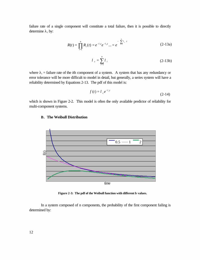
B. The Weibull Distribution
In a system composed of n components, the probability of the first component failing isdetermined by:
time
f(t)
0.5 1 2
Figure 2-3: The pdf of the Weibull function with different b values.
(2-13a)
(2-13b)
(2-14)
13
∏=
=n
ii tFtF
1
)()(
where Fi is the probability of failure of the ith component. For systems where all componentsexhibit uniform failure rates, the probability of failure of the system can be expressed as:
( )ntetF λ−−= 1)(
This model is called the Weibull model. It is conventionally written as:
( )βαββ βα tettf −−= 1)( and 1)( −= ββ βαλ tt
where
α = the scale parameter
β = the shape parameter
The shape parameter enables the Weibull distribution to model multiple aging trends:
• If 0 < β < 1, then λ(t) is decreasing with time
• If β =1 then λ(t) is constant è the exponential model
• If 1 < β < ∞ then λ(t) is increasing with time.
For the Weibull distribution, the MTTF is given as:
+Γ=
βα1
11
MTTF
where Γ is the gamma function, which is defined as:
∫∞
−−=Γ0
1)( dtetx tx for x>0
(2-15a)
(2-15b)
(2-16)
(2-17)
(2-18)
14
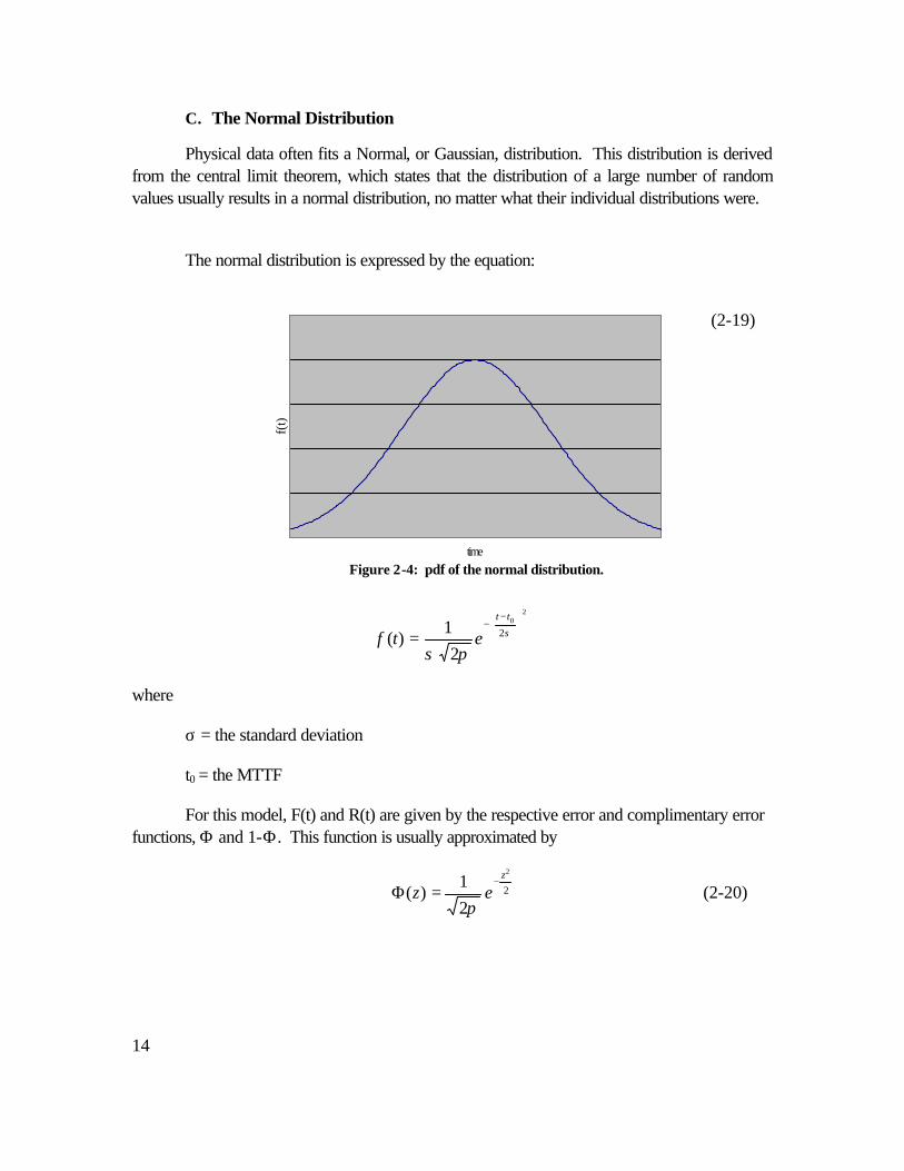
C. The Normal Distribution
Physical data often fits a Normal, or Gaussian, distribution. This distribution is derivedfrom the central limit theorem, which states that the distribution of a large number of randomvalues usually results in a normal distribution, no matter what their individual distributions were.
The normal distribution is expressed by the equation:
20
2
21
)(
−−
= σ
πσ
tt
etf
where
σ = the standard deviation
t0 = the MTTF
For this model, F(t) and R(t) are given by the respective error and complimentary errorfunctions, Φ and 1-Φ. This function is usually approximated by
2
2
21
)(z
ez−
=Φπ
time
f(t)
Figure 2-4: pdf of the normal distribution.
(2-19)
(2-20)
15
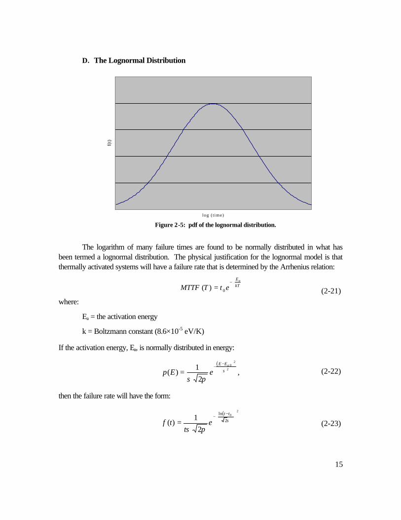
D. The Lognormal Distribution
The logarithm of many failure times are found to be normally distributed in what hasbeen termed a lognormal distribution. The physical justification for the lognormal model is thatthermally activated systems will have a failure rate that is determined by the Arrhenius relation:
−
= kTEa
etTMTTF 0)(
where:
Ea = the activation energy
k = Boltzmann constant (8.6×10⁻⁵ eV/K)
If the activation energy, Ea, is normally distributed in energy:
( )2
20
21
)( σ
πσ
aEE
eEp−
−= ,
then the failure rate will have the form:
( ) 20
2ln
21
)(
−−
= σ
πσ
tt
et
tf
log ( t ime)
f(t)
Figure 2-5: pdf of the lognormal distribution.
(2-21)
(2-22)
(2-23)
16
For this model, F(t) is given by
( )
−
Φσ
0ln tt
III. Application of Reliability Models
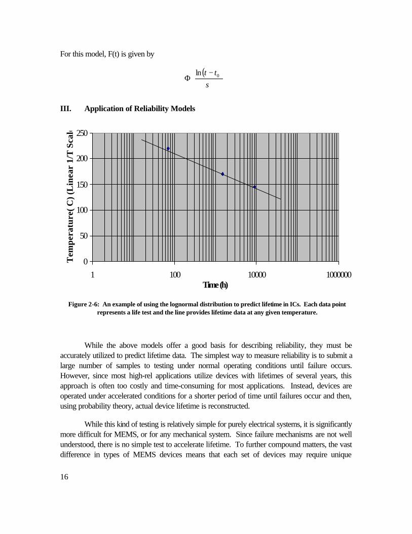
While the above models offer a good basis for describing reliability, they must beaccurately utilized to predict lifetime data. The simplest way to measure reliability is to submit alarge number of samples to testing under normal operating conditions until failure occurs.However, since most high-rel applications utilize devices with lifetimes of several years, thisapproach is often too costly and time-consuming for most applications. Instead, devices areoperated under accelerated conditions for a shorter period of time until failures occur and then,using probability theory, actual device lifetime is reconstructed.
While this kind of testing is relatively simple for purely electrical systems, it is significantlymore difficult for MEMS, or for any mechanical system. Since failure mechanisms are not wellunderstood, there is no simple test to accelerate lifetime. To further compound matters, the vastdifference in types of MEMS devices means that each set of devices may require unique
0
50
100
150
200
250
1 100 10000 1000000Time (h)
Tem
pera
ture
( C) (
Lin
ear
1/T
Sca
le)
Figure 2-6: An example of using the lognormal distribution to predict lifetime in ICs. Each data pointrepresents a life test and the line provides lifetime data at any given temperature.
17
acceleration conditions. These kinds of difficulties are not encountered in purely electricalsystems because lifetime is determined almost exclusively by the rate of thermally activatedprocesses. These interactions are easy to accelerate by increasing temperature. In MEMS, onthe other hand, it may be temperature, humidity, vibration, or a number of other factors that limitdevice lifetime, and accelerating one failure mode may decelerate another.
Once life-test data is collected, it can be modeled with one of the above probabilitydistributions. Take, for example, data that fits a lognormal distribution. This can be determinedby plotting the data on a lognormal graph. If the life-test data fits into a straight line, then thedata fits into a lognormal distribution. The intersection of this straight line with 50% cumulativefailure indicates the MTTF.
To accurately predict lifetime at any operating conditions, at least three distinct highstress tests must be performed. The median lifetime from each of the three tests is thentransferred onto a lognormal plot and fit with a line. Median life at any operating condition canthen be determined.
In a world with limitless resources and time, lifetime test would be conducted with nearlyinfinite sample sizes. Since this is a practical impossibility, the size of the sample must beconsidered in determining the confidence in lifetime predictions. Confidence is expressed interms of a percentage, where a confidence value says that for a given percentage of the time, atest would yield a result within the two limits of the test. Thus an upper and lower confidence of90% on respective lifetimes of two and four years means that nine out of every ten tests wouldpredict a lifetime between two and four years. The following equations yield confidencelimits:[118]
upper limit = T test
t df alpha Ne× ×( ( , ) / )σ
lower limit =T test
t df alpha Ne× − ×( ( , ) / )σ
where
σ2 = the standard deviation in the data
Ttest = median life at test temperature
t(df, alpha) = value from the Students’ t distribution (see ref. [118] for more detail onthis subject)
df = degrees of freedom (N-1)
alpha = (1% confidence) / 2
(2-24a)
(2-24b)
18
N = sample size
Due to the variability of test data, it should be apparent that an understanding of failuremechanisms within MEMS is critical to determining device lifetime. This kind of information canonly be determined from further research into MEMS reliability. As stated above, the diversityof MEMS technologies on the market almost necessitates an individualized approach to astatistical lifetime study. One of the great obstacles to space qualifying MEMS is theindividuality of the devices. MEMS manufacturers do not have the luxury of ASIC and MMICdesigners, who can use a great deal of prior work and knowledge in space qualifying theirproducts. Despite these obstacles, it is inevitable that MEMS will eventually work their wayinto high-rel applications and this methodology will provide the means for realizing that goal.
IV. Failure
While this chapter has devoted a lot of time to quantifying reliability, it has not discussedthe roots of reliability, namely failure. The time dependence of reliability, R, and failure, F, arecomplimentary, so the rates are both equal to the failure rate, λ. In order to accurately studyMEMS reliability, the nature of failures must be quantified. Failure may be separated into twodistinct categories:
(1) Degradation failure, which consists of device operation departing far enough fromnormal conditions that the component can no longer be trusted for reliable operation
(2) Catastrophic failures, which are, as the name implies, the complete end of deviceoperation.
Failures occur when the stresses on a device exceed its strength. While the mostprevalent failure mechanisms in MEMS are not yet fully understood, there is a great deal ofknowledge about failure mechanisms within more common semiconductor devices, which shouldhave a bearing upon failure within MEMS.
In order for a device to be classified as high-rel, it must meet some basic criteria. Themost significant of these is that a device cannot exhibit a dominant failure mechanism. Thisensures that there is no inherent design flaw that prohibits long-term reliable device operation.In order to make this assessment, the failure mechanisms with a device must beunderstood.[109]
The identification and mitigation of failure mechanisms in MEMS is both one of the mostimportant and one of the newest issues in MEMS. The most relevant way to keep abreast ofthe failure mechanisms within MEMS is to search the current literature, as data contained withinthis manual is almost sure to be revised after publication. With this in mind, Chapter 3, “Failure

19
Modes and Mechanisms” provides a description of the most commonly observed failuremechanisms and associated failure modes in MEMS.
V. Additional Reading
E. A. Amerasekera and F. N. Najm, Failure Mechanisms in Semiconductor Devices: SecondEdition, John Wiley & Sons, New York, 1997.
C. C. Montgomery and G. C. Runger, Applied Statistics and Probability for Engineers, JohnWiley & Sons: New York, 1994.

20
21
Chapter 3: Failure Modes and Mechanisms
B. Stark
A critical part of understanding the reliability of any system comes from understandingthe possible ways in which the system may fail. In MEMS, there are several failure mechanismsthat have been found to be the primary sources of failure within devices. In comparison toelectronic circuits, these failure mechanisms are not well understood nor easy to accelerate forlife testing. In any discussion of failures, the definition of failure mechanisms, or causes of failure,often overlaps with the definition of failure modes, or observable failure events. To alleviate thisconfusion this chapter has been roughly organized by failure modes, with mechanisms beingdescribed within the sections on the modes they cause. Failure mechanisms that do not haveclearly associated modes are discussed at the end of this chapter.
I. Mechanical Fracture
Mechanical fracture is defined as the breaking of a uniform material into two separatesections. In MEMS it will usually lead to the catastrophic failure of a device, although there aresome structures that will have more moderate performance degradations.[5,8] No matter whatthe actual outcome, any fracturing is a serious reliability concern. There are three types offractures, ductile, brittle, and intercrystalline fracture. Ductile fracture, as the name implies,occurs in ductile materials. It is characterized by almost uninterrupted plastic deformation of amaterial. It is usually signified by the necking, or extreme thinning, of a material at one specificpoint. Brittle fracture occurs along crystal planes and develops rapidly with little deformation.Intercrystalline fracture is a brittle fracture that occurs along grain boundaries in polycrystallinematerials, often beginning at a point where impurities or precipitates accumulate. For MEMSthe latter two types of fracture are more common. To understand the actual causes of fractureand the methods for predicting it, several terms must be first defined.[27]
A. Definitions
Mechanical failure in a crystal lattice occurs when an applied stress exceeds the failurestress of the structure. Stresses are separated into the two categories of normal and shearstress. Normal stress is defined as stress perpendicular to a plane in a material, while shearstress occurs parallel to a plane, as shown in Figure 3-1. In solid materials, stress is linearlyrelated to a concept called strain, which is the fractional elongation of a material. Theproportionality constant between stress and strain is, for small normal loads, called the modulusof elasticity, or Young’s modulus. The actual deformation of a cubic volume will depend uponall the stresses applied to it:
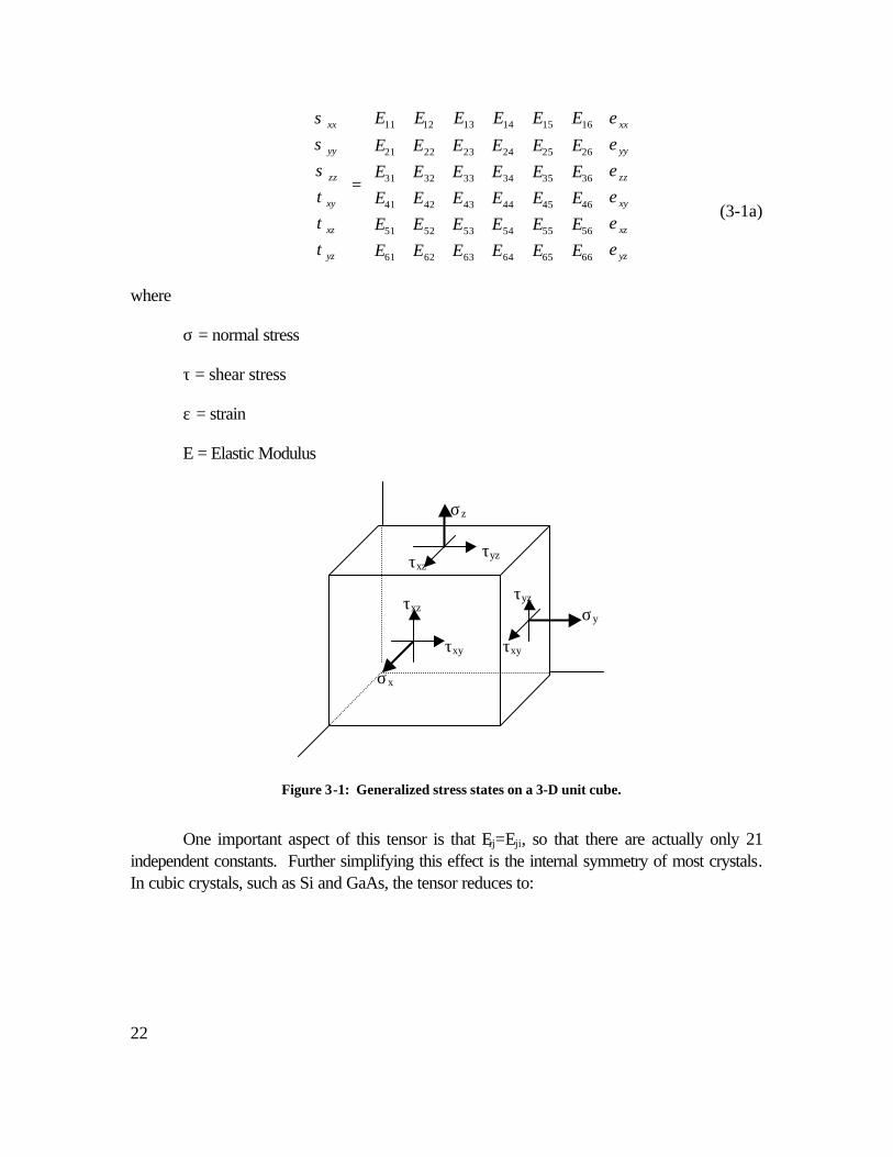
22
=
yz
xz
xy
zz
yy
xx
yz
xz
xy
zz
yy
xx
EEEEEEEEEEEEEEEEEEEEEEEEEEEEEE
EEEEEE
εεεεεε
τττσσσ
666564636261
565554535251
464544434241
363534333231
262524232221
161514131211
where
σ = normal stress
τ = shear stress
ε = strain
E = Elastic Modulus
One important aspect of this tensor is that Eij=Eji, so that there are actually only 21independent constants. Further simplifying this effect is the internal symmetry of most crystals.In cubic crystals, such as Si and GaAs, the tensor reduces to:
τxz
τxy
σx
σy
σz
τxzτyz
τyz
τxy
Figure 3-1: Generalized stress states on a 3-D unit cube.
(3-1a)
23
=
yz
xz
xy
zz
yy
xx
yz
xz
xy
zz
yy
xx
EE
EEEEEEEEEE
εεεεεε
τττσσσ
44
44
44
111212
121112
121211
000000000000000000000000
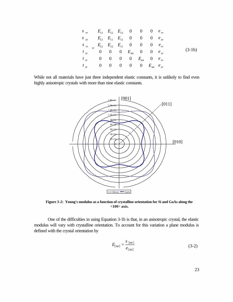
While not all materials have just three independent elastic constants, it is unlikely to find evenhighly anisotropic crystals with more than nine elastic constants.
One of the difficulties in using Equation 3-1b is that, in an anisotropic crystal, the elasticmodulus will vary with crystalline orientation. To account for this variation a plane modulus isdefined with the crystal orientation by
[ ][ ]
[ ]hkl
hklhklE
εσ
=
0
2E+10
4E+10
6E+10
8E+10
1E+11
1.2E+11
1.4E+11
1.6E+11
1.8E+11
Silicon GaAs
Figure 3-2: Young's modulus as a function of crystalline orientation for Si and GaAs along the<100> axis.
[010]
[011][001]
(3-1b)
(3-2)
24
In order to relate the modulus of a crystalline plane to the elastic constants in Equations3-1, the following equation is used:
)))(5.0(2),,( 23
21
23
22
22
2144121111
1 llllllssssE ++−−−=− ψφθ
where
))(2( 12111211
121111 EEEE
EEs
−++
=
))(2( 12111211
1212 EEEE
Es
−+−
=
44
441
Es =
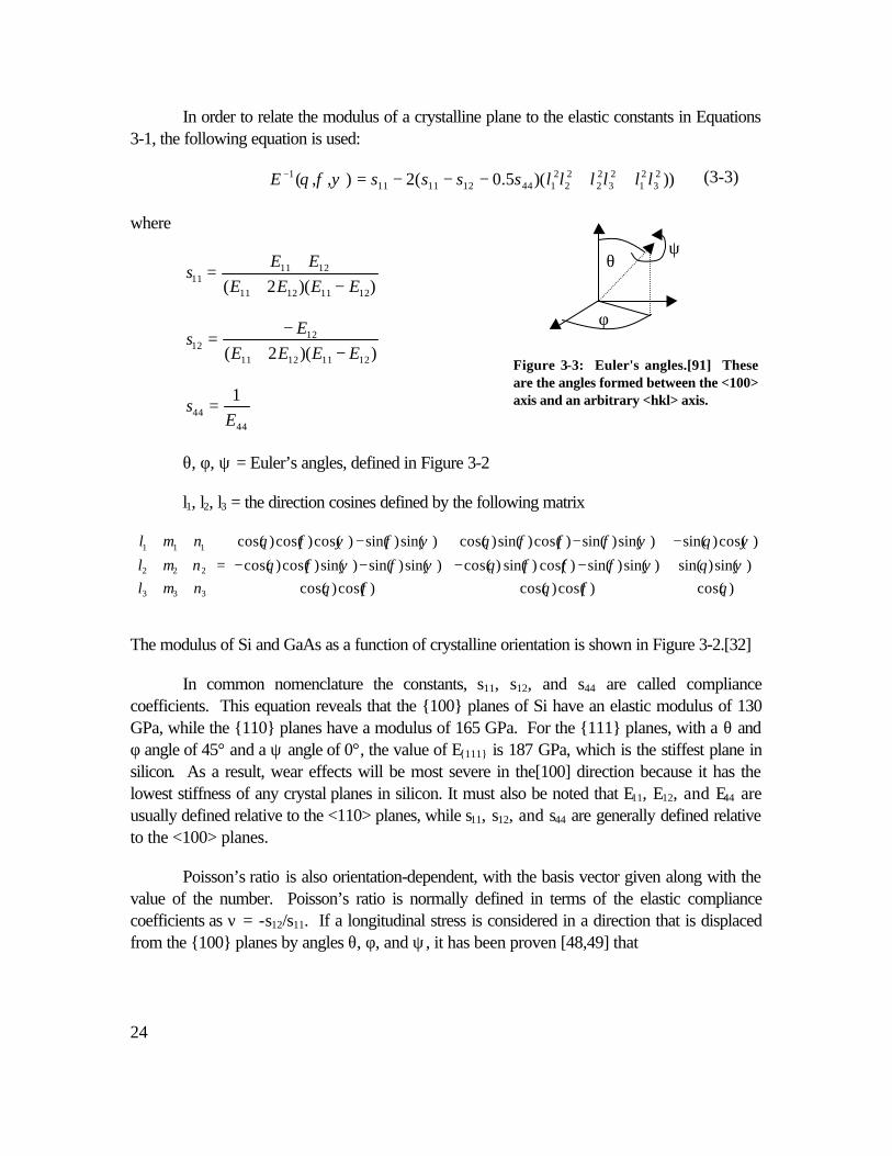
θ, φ, ψ = Euler’s angles, defined in Figure 3-2
l1, l2, l3 = the direction cosines defined by the following matrix
−−−−
−−−
=
)cos()cos()cos()cos()cos()sin()sin()sin()sin()cos()sin()cos()sin()sin()sin()cos()cos(
)cos()sin()sin()sin()cos()sin()cos()sin()sin()cos()cos()cos(
333
222
111
θφθφθψθψφφφθψφψφθ
ψθψφφφθψφψφθ
nmlnml
nml
The modulus of Si and GaAs as a function of crystalline orientation is shown in Figure 3-2.[32]
In common nomenclature the constants, s11, s12, and s44 are called compliancecoefficients. This equation reveals that the 100 planes of Si have an elastic modulus of 130GPa, while the 110 planes have a modulus of 165 GPa. For the 111 planes, with a θ andφ angle of 45° and a ψ angle of 0°, the value of E111 is 187 GPa, which is the stiffest plane insilicon. As a result, wear effects will be most severe in the[100] direction because it has thelowest stiffness of any crystal planes in silicon. It must also be noted that E11, E12, and E44 areusually defined relative to the <110> planes, while s11, s12, and s44 are generally defined relativeto the <100> planes.
Poisson’s ratio is also orientation-dependent, with the basis vector given along with thevalue of the number. Poisson’s ratio is normally defined in terms of the elastic compliancecoefficients as ν = -s12/s11. If a longitudinal stress is considered in a direction that is displacedfrom the 100 planes by angles θ, φ, and ψ, it has been proven [48,49] that
θ
φ
ψ
Figure 3-3: Euler's angles.[91] Theseare the angles formed between the <100>axis and an arbitrary <hkl> axis.
(3-3)
25
( )( )
( )( )23
21
23
22
21
2144121111
23
23
22
22
21
2144121112
5.25.
llllllssssmlmlmlssss
++−−−++−−+
−=ν
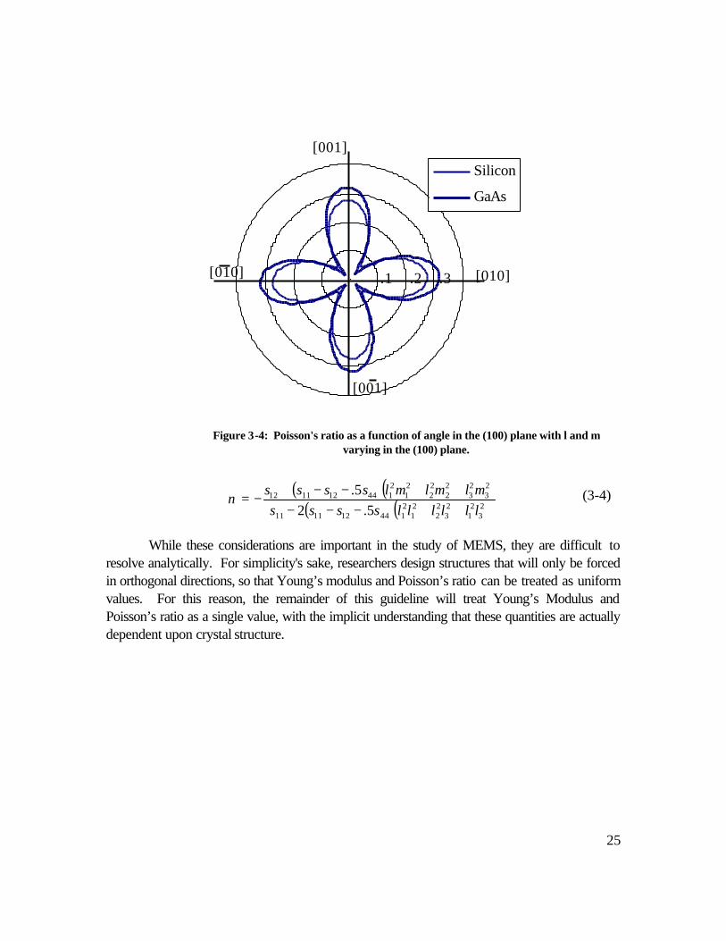
While these considerations are important in the study of MEMS, they are difficult toresolve analytically. For simplicity's sake, researchers design structures that will only be forcedin orthogonal directions, so that Young’s modulus and Poisson’s ratio can be treated as uniformvalues. For this reason, the remainder of this guideline will treat Young’s Modulus andPoisson’s ratio as a single value, with the implicit understanding that these quantities are actuallydependent upon crystal structure.
Silicon
GaAs
[010]
[001]
[010]
[001]
.1 .2 .3
Figure 3-4: Poisson's ratio as a function of angle in the (100) plane with l and mvarying in the (100) plane.
(3-4)
26
Once the definitions of stress and strain are understood, it is possible to understand howstress leads to failure.
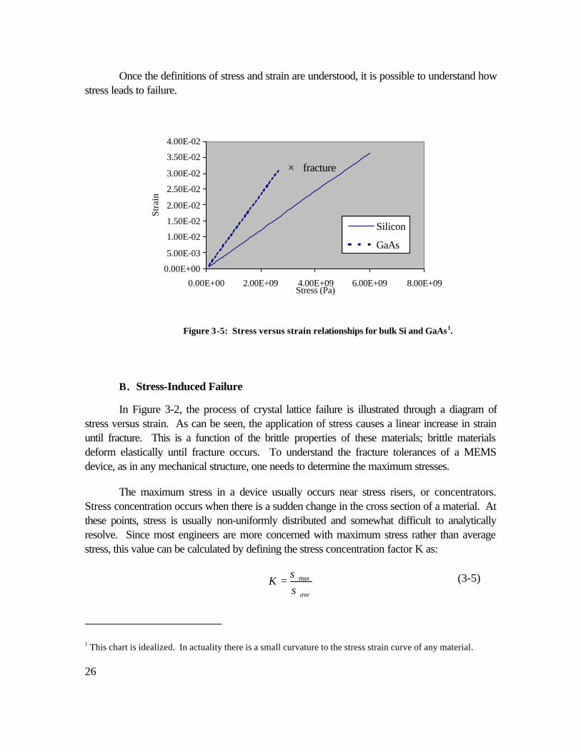
B. Stress-Induced Failure
In Figure 3-2, the process of crystal lattice failure is illustrated through a diagram ofstress versus strain. As can be seen, the application of stress causes a linear increase in strainuntil fracture. This is a function of the brittle properties of these materials; brittle materialsdeform elastically until fracture occurs. To understand the fracture tolerances of a MEMSdevice, as in any mechanical structure, one needs to determine the maximum stresses.
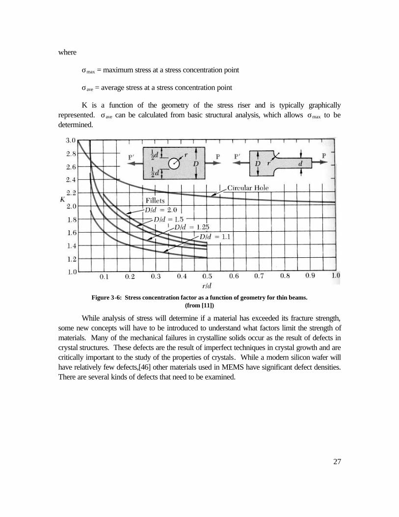
The maximum stress in a device usually occurs near stress risers, or concentrators.Stress concentration occurs when there is a sudden change in the cross section of a material. Atthese points, stress is usually non-uniformly distributed and somewhat difficult to analyticallyresolve. Since most engineers are more concerned with maximum stress rather than averagestress, this value can be calculated by defining the stress concentration factor K as:
ave
Kσσ max=
1 This chart is idealized. In actuality there is a small curvature to the stress strain curve of any material.
Figure 3-5: Stress versus strain relationships for bulk Si and GaAs1.
0.00E+00
5.00E-03
1.00E-02
1.50E-02
2.00E-02
2.50E-02
3.00E-02
3.50E-02
4.00E-02
0.00E+00 2.00E+09 4.00E+09 6.00E+09 8.00E+09Stress (Pa)
Stra
in
Silicon
GaAs
× fracture
(3-5)
27
where
σmax = maximum stress at a stress concentration point
σave = average stress at a stress concentration point
K is a function of the geometry of the stress riser and is typically graphicallyrepresented. σave can be calculated from basic structural analysis, which allows σmax to bedetermined.
Figure 3-6: Stress concentration factor as a function of geometry for thin beams.(from [11])
While analysis of stress will determine if a material has exceeded its fracture strength,some new concepts will have to be introduced to understand what factors limit the strength ofmaterials. Many of the mechanical failures in crystalline solids occur as the result of defects incrystal structures. These defects are the result of imperfect techniques in crystal growth and arecritically important to the study of the properties of crystals. While a modern silicon wafer willhave relatively few defects,[46] other materials used in MEMS have significant defect densities.There are several kinds of defects that need to be examined.
28
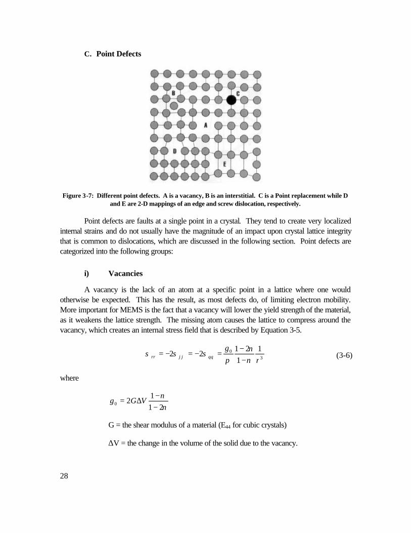
C. Point Defects
Figure 3-7: Different point defects. A is a vacancy, B is an interstitial. C is a Point replacement while Dand E are 2-D mappings of an edge and screw dislocation, respectively.
Point defects are faults at a single point in a crystal. They tend to create very localizedinternal strains and do not usually have the magnitude of an impact upon crystal lattice integritythat is common to dislocations, which are discussed in the following section. Point defects arecategorized into the following groups:
i) Vacancies
A vacancy is the lack of an atom at a specific point in a lattice where one wouldotherwise be expected. This has the result, as most defects do, of limiting electron mobility.More important for MEMS is the fact that a vacancy will lower the yield strength of the material,as it weakens the lattice strength. The missing atom causes the lattice to compress around thevacancy, which creates an internal stress field that is described by Equation 3-5.
30 1
121
22r
grr ν
νπ
σσσ θθϕϕ −−
=−=−=
where
νν21
120 −
−∆= VGg
G = the shear modulus of a material (E44 for cubic crystals)
∆V = the change in the volume of the solid due to the vacancy.
(3-6)
29
ii) Interstitial
An interstitial is an additional atom which has become wedged between the atoms of alattice. An interstitial will have, to a first order approximation, the same stress field as avacancy, except that the strength factor, g0, becomes
300 21
13
8r
Gg η
ννπ
−+
=
where
10 −Α
≈r
η
r0 = the radius of the foreign atom
A = the lattice parameter
iii) Point Replacement
In this case a single atom has been replaced by an atom of a different element. Oftenthis is done intentionally for doping purposes, but sometimes it occurs accidentally as the resultof disorder in the lattice or impurities in the melt. Theses defects will have differing effects on themechanical properties of solids, but will usually not be as large in magnitude as vacancies orinterstitials.[53]
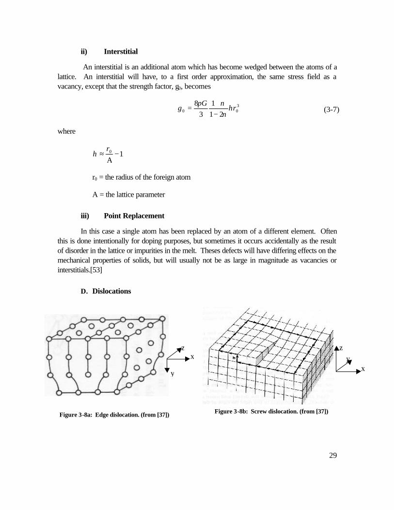
D. Dislocations
x z
y
Figure 3-8a: Edge dislocation. (from [37]) Figure 3-8b: Screw dislocation. (from [37])
(3-7)
x
z y
30
A dislocation is a one-dimensional array of point defects in an otherwise perfect crystal.They occur when a crystal is subjected to stresses that exceed the elastic limits of materials.Dislocations are usually introduced into a crystal through the presence of a temperature gradientduring crystal growth. Modern wafer processing techniques produce extremely low dislocationdensities on wafers. Dislocations can be separated into two types:
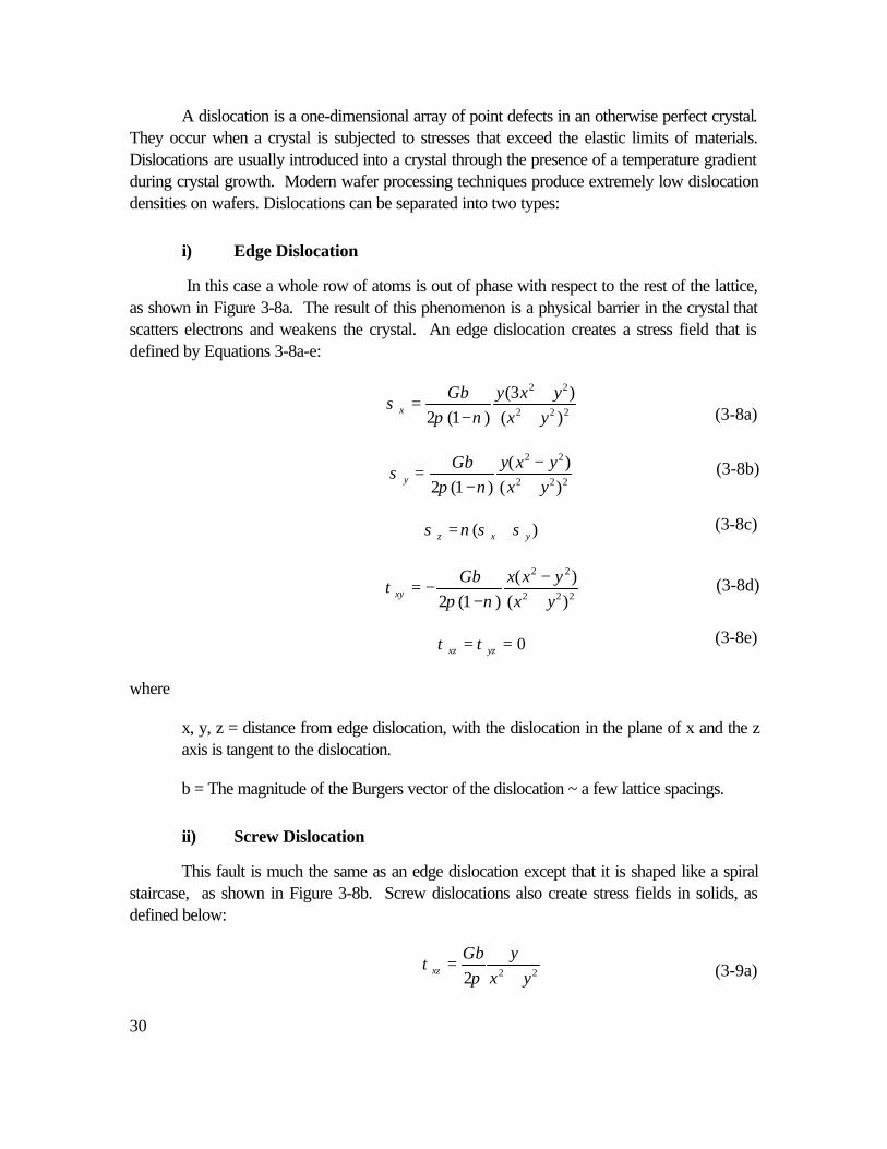
i) Edge Dislocation
In this case a whole row of atoms is out of phase with respect to the rest of the lattice,as shown in Figure 3-8a. The result of this phenomenon is a physical barrier in the crystal thatscatters electrons and weakens the crystal. An edge dislocation creates a stress field that isdefined by Equations 3-8a-e:
222
22
)()3(
)1(2 yxyxyGb
x ++
−=
νπσ
222
22
)()(
)1(2 yxyxyGb
y +−
−=
νπσ
)( yxz σσνσ +=
222
22
)()(
)1(2 yxyxxGb
xy +−
−−=
νπτ
0== yzxz ττ
where
x, y, z = distance from edge dislocation, with the dislocation in the plane of x and the zaxis is tangent to the dislocation.
b = The magnitude of the Burgers vector of the dislocation ~ a few lattice spacings.
ii) Screw Dislocation
This fault is much the same as an edge dislocation except that it is shaped like a spiralstaircase, as shown in Figure 3-8b. Screw dislocations also create stress fields in solids, asdefined below:
222 yxyGb
xz +=
πτ
(3-8a)
(3-8b)
(3-8c)
(3-8d)
(3-8e)
(3-9a)
31
222 yxxGb
yz +−=
πτ
0==== xyzyx τσσσ
The essential feature to recognize from these equations is that dislocations introducestresses internal to materials that will significantly weaken crystal lattices. While these stressesdecrease quadratically with distance from the dislocation, there clearly will be a strong localinternal stress created by these features. Another factor to consider is that the stress fields fromdifferent dislocations will interact, creating internal forces. From a MEMS reliability standpoint,this means that using high quality wafers with smaller numbers of dislocations will ultimatelyincrease device reliability and lifetime. For more information on this subject, Reference [37],“Elementary Dislocation Theory” by Weertman and Weertman offers a good, in-depthdiscussion of dislocation theory.
E. Precipitates
In metals containing another element in a supersaturated solid solution, this solutiontends to precipitate in the form of a compound with the solvent metal.[53] In the presence of adislocation, atoms will precipitate into the dislocation, which will occur at the rate:
3/2
)(
∝
Tt
tn
where
n(t) = the number of atoms precipitating in a time, t.
T = temperature
This phenomenon is used to harden materials by allowing precipitates to lock dislocationand prevent them from moving through the lattice. While this is found to be useful inconstruction materials, it creates problems for MEMS devices using metallic compounds, suchas GaAs. The formation of precipitates creates an internal stress, which can significantlyweaken crystal lattices and is discussed in great detail in Reference [53].
(3-9b)
(3-9c)
(3-10)
32
F. Fracture Strength
The impetus for studying defects is that, for brittle materials, the fracture strength is afunction of the largest crystal defect. For a defect of length c, the fracture strength can bedetermined by:[114]
cYK lc
F =σ
where
Klc = Fracture toughness
σf = fracture strength
Y = dimensionless parameter that depends on the geometry of the flaw
It is sometimes useful to approximate the defect as being penny shaped with a radius, c,in which case the fracture strength is:[17]
cK lc
Fπ
σ6.1
=
Normally, a Gaussian distribution of crystal defects is assumed for a given volume. Thiswould imply that there is also a normal distribution of fracture strengths, as described below:
2
2
2
)(
212 )2()( dedf
σσ
πσ−
−−=
where
d2 = standard deviation in fracture strength
σ = mean fracture strength
For this kind of fracture stress distribution, the probability of failure of a body exposedto a stress field is modeled by the Weibull probability distribution function of:
∫−=
−−
v
m
u dv
f eP 01 σ
σσ
[40]
where
(3-11)
(3-12)
(3-13)
(3-14)
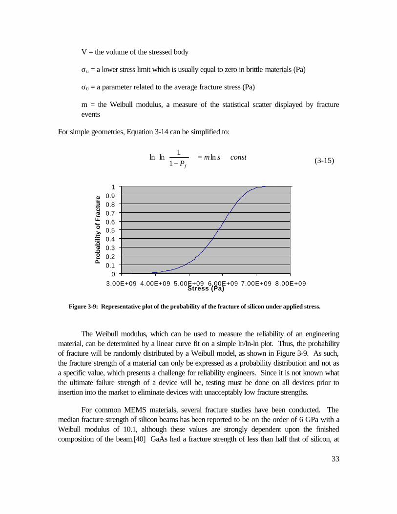
33
V = the volume of the stressed body
σu = a lower stress limit which is usually equal to zero in brittle materials (Pa)
σ0 = a parameter related to the average fracture stress (Pa)
m = the Weibull modulus, a measure of the statistical scatter displayed by fractureevents
For simple geometries, Equation 3-14 can be simplified to:
constmPf
+=
−σln
11
lnln
The Weibull modulus, which can be used to measure the reliability of an engineeringmaterial, can be determined by a linear curve fit on a simple ln/ln-ln plot. Thus, the probabilityof fracture will be randomly distributed by a Weibull model, as shown in Figure 3-9. As such,the fracture strength of a material can only be expressed as a probability distribution and not asa specific value, which presents a challenge for reliability engineers. Since it is not known whatthe ultimate failure strength of a device will be, testing must be done on all devices prior toinsertion into the market to eliminate devices with unacceptably low fracture strengths.
For common MEMS materials, several fracture studies have been conducted. Themedian fracture strength of silicon beams has been reported to be on the order of 6 GPa with aWeibull modulus of 10.1, although these values are strongly dependent upon the finishedcomposition of the beam.[40] GaAs had a fracture strength of less than half that of silicon, at
00.10.20.30.40.50.60.70.80.9
1
3.00E+09 4.00E+09 5.00E+09 6.00E+09 7.00E+09 8.00E+09Stress (Pa)
Pro
babi
lity
of F
ract
ure
Figure 3-9: Representative plot of the probability of the fracture of silicon under applied stress.
(3-15)
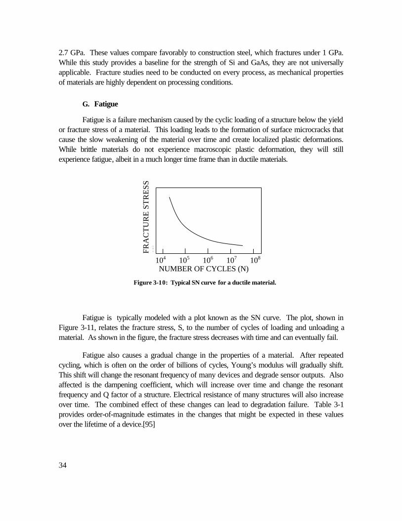
34
2.7 GPa. These values compare favorably to construction steel, which fractures under 1 GPa.While this study provides a baseline for the strength of Si and GaAs, they are not universallyapplicable. Fracture studies need to be conducted on every process, as mechanical propertiesof materials are highly dependent on processing conditions.
G. Fatigue
Fatigue is a failure mechanism caused by the cyclic loading of a structure below the yieldor fracture stress of a material. This loading leads to the formation of surface microcracks thatcause the slow weakening of the material over time and create localized plastic deformations.While brittle materials do not experience macroscopic plastic deformation, they will stillexperience fatigue, albeit in a much longer time frame than in ductile materials.
Fatigue is typically modeled with a plot known as the SN curve. The plot, shown inFigure 3-11, relates the fracture stress, S, to the number of cycles of loading and unloading amaterial. As shown in the figure, the fracture stress decreases with time and can eventually fail.
Fatigue also causes a gradual change in the properties of a material. After repeatedcycling, which is often on the order of billions of cycles, Young’s modulus will gradually shift.This shift will change the resonant frequency of many devices and degrade sensor outputs. Alsoaffected is the dampening coefficient, which will increase over time and change the resonantfrequency and Q factor of a structure. Electrical resistance of many structures will also increaseover time. The combined effect of these changes can lead to degradation failure. Table 3-1provides order-of-magnitude estimates in the changes that might be expected in these valuesover the lifetime of a device.[95]
104 105 106 107 108
FRA
CT
UR
E S
TR
ESS
(S)
NUMBER OF CYCLES (N)
Figure 3-10: Typical SN curve for a ductile material.
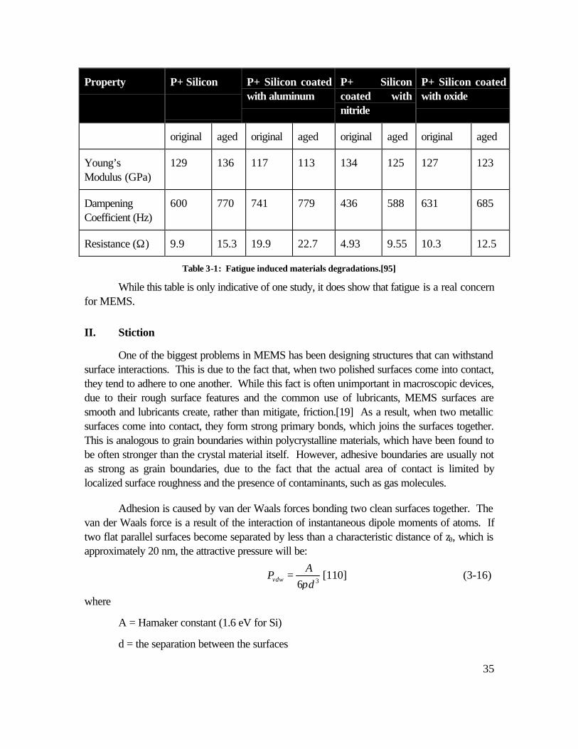
35
Property P+ Silicon P+ Silicon coatedwith aluminum
P+ Siliconcoated withnitride
P+ Silicon coatedwith oxide
original aged original aged original aged original aged
Young’sModulus (GPa)
129 136 117 113 134 125 127 123
DampeningCoefficient (Hz)
600 770 741 779 436 588 631 685
Resistance (Ω) 9.9 15.3 19.9 22.7 4.93 9.55 10.3 12.5
Table 3-1: Fatigue induced materials degradations.[95]
While this table is only indicative of one study, it does show that fatigue is a real concernfor MEMS.
II. Stiction
One of the biggest problems in MEMS has been designing structures that can withstandsurface interactions. This is due to the fact that, when two polished surfaces come into contact,they tend to adhere to one another. While this fact is often unimportant in macroscopic devices,due to their rough surface features and the common use of lubricants, MEMS surfaces aresmooth and lubricants create, rather than mitigate, friction.[19] As a result, when two metallicsurfaces come into contact, they form strong primary bonds, which joins the surfaces together.This is analogous to grain boundaries within polycrystalline materials, which have been found tobe often stronger than the crystal material itself. However, adhesive boundaries are usually notas strong as grain boundaries, due to the fact that the actual area of contact is limited bylocalized surface roughness and the presence of contaminants, such as gas molecules.
Adhesion is caused by van der Waals forces bonding two clean surfaces together. Thevan der Waals force is a result of the interaction of instantaneous dipole moments of atoms. Iftwo flat parallel surfaces become separated by less than a characteristic distance of z0, which isapproximately 20 nm, the attractive pressure will be:
36 dA
Pvdw π= [110]
where
A = Hamaker constant (1.6 eV for Si)
d = the separation between the surfaces
(3-16)
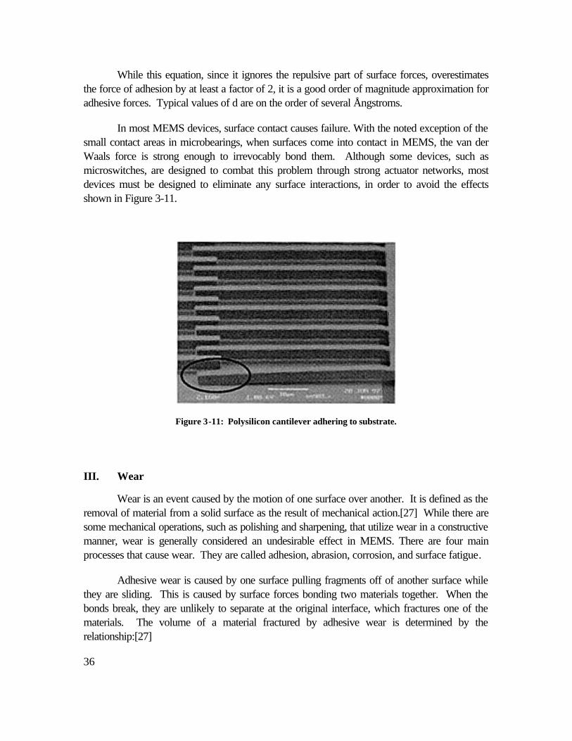
36
While this equation, since it ignores the repulsive part of surface forces, overestimatesthe force of adhesion by at least a factor of 2, it is a good order of magnitude approximation foradhesive forces. Typical values of d are on the order of several Ångstroms.
In most MEMS devices, surface contact causes failure. With the noted exception of thesmall contact areas in microbearings, when surfaces come into contact in MEMS, the van derWaals force is strong enough to irrevocably bond them. Although some devices, such asmicroswitches, are designed to combat this problem through strong actuator networks, mostdevices must be designed to eliminate any surface interactions, in order to avoid the effectsshown in Figure 3-11.
Figure 3-11: Polysilicon cantilever adhering to substrate.
III. Wear
Wear is an event caused by the motion of one surface over another. It is defined as theremoval of material from a solid surface as the result of mechanical action.[27] While there aresome mechanical operations, such as polishing and sharpening, that utilize wear in a constructivemanner, wear is generally considered an undesirable effect in MEMS. There are four mainprocesses that cause wear. They are called adhesion, abrasion, corrosion, and surface fatigue.
Adhesive wear is caused by one surface pulling fragments off of another surface whilethey are sliding. This is caused by surface forces bonding two materials together. When thebonds break, they are unlikely to separate at the original interface, which fractures one of thematerials. The volume of a material fractured by adhesive wear is determined by therelationship:[27]
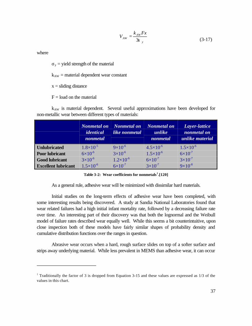
37
y
AWAW
FxkV
σ3=
where
σy = yield strength of the material
kAW = material dependent wear constant
x = sliding distance
F = load on the material
kAW is material dependent. Several useful approximations have been developed fornon-metallic wear between different types of materials:
Nonmetal onidenticalnonmetal
Nonmetal onlike nonmetal
Nonmetal onunlike
nonmetal
Layer-latticenonmetal on
unlike material
Unlubricated 1.8×10⁻⁵ 9×10⁻⁶ 4.5×10⁻⁶ 1.5×10⁻⁶
Poor lubricant 6×10⁻⁶ 3×10⁻⁶ 1.5×10⁻⁶ 6×10⁻⁷
Good lubricant 3×10⁻⁶ 1.2×10⁻⁶ 6×10⁻⁷ 3×10⁻⁷
Excellent lubricant 1.5×10⁻⁶ 6×10⁻⁷ 3×10⁻⁷ 9×10⁻⁸
Table 3-2: Wear coefficients for nonmetals1.[120]
As a general rule, adhesive wear will be minimized with dissimilar hard materials.
Initial studies on the long-term effects of adhesive wear have been completed, withsome interesting results being discovered. A study at Sandia National Laboratories found thatwear related failures had a high initial infant mortality rate, followed by a decreasing failure rateover time. An interesting part of their discovery was that both the lognormal and the Weibullmodel of failure rates described wear equally well. While this seems a bit counterintuitive, uponclose inspection both of these models have fairly similar shapes of probability density andcumulative distribution functions over the ranges in question.
Abrasive wear occurs when a hard, rough surface slides on top of a softer surface andstrips away underlying material. While less prevalent in MEMS than adhesive wear, it can occur
1 Traditionally the factor of 3 is dropped from Equation 3-15 and these values are expressed as 1/3 of thevalues in this chart.
(3-17)
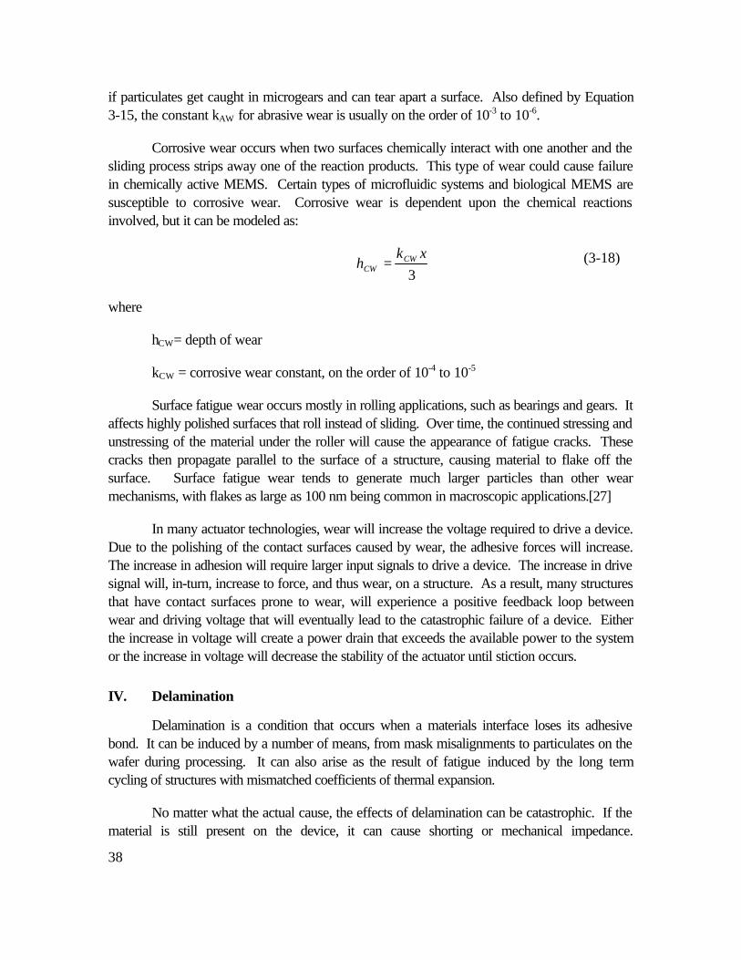
38
if particulates get caught in microgears and can tear apart a surface. Also defined by Equation3-15, the constant kAW for abrasive wear is usually on the order of 10-3 to 10-6.
Corrosive wear occurs when two surfaces chemically interact with one another and thesliding process strips away one of the reaction products. This type of wear could cause failurein chemically active MEMS. Certain types of microfluidic systems and biological MEMS aresusceptible to corrosive wear. Corrosive wear is dependent upon the chemical reactionsinvolved, but it can be modeled as:
3xk
h CWCW =
where
hCW= depth of wear
kCW = corrosive wear constant, on the order of 10-4 to 10-5
Surface fatigue wear occurs mostly in rolling applications, such as bearings and gears. Itaffects highly polished surfaces that roll instead of sliding. Over time, the continued stressing andunstressing of the material under the roller will cause the appearance of fatigue cracks. Thesecracks then propagate parallel to the surface of a structure, causing material to flake off thesurface. Surface fatigue wear tends to generate much larger particles than other wearmechanisms, with flakes as large as 100 nm being common in macroscopic applications.[27]
In many actuator technologies, wear will increase the voltage required to drive a device.Due to the polishing of the contact surfaces caused by wear, the adhesive forces will increase.The increase in adhesion will require larger input signals to drive a device. The increase in drivesignal will, in-turn, increase to force, and thus wear, on a structure. As a result, many structuresthat have contact surfaces prone to wear, will experience a positive feedback loop betweenwear and driving voltage that will eventually lead to the catastrophic failure of a device. Eitherthe increase in voltage will create a power drain that exceeds the available power to the systemor the increase in voltage will decrease the stability of the actuator until stiction occurs.
IV. Delamination
Delamination is a condition that occurs when a materials interface loses its adhesivebond. It can be induced by a number of means, from mask misalignments to particulates on thewafer during processing. It can also arise as the result of fatigue induced by the long termcycling of structures with mismatched coefficients of thermal expansion.
No matter what the actual cause, the effects of delamination can be catastrophic. If thematerial is still present on the device, it can cause shorting or mechanical impedance.
(3-18)
39
Furthermore, the loss of mass will alter the mechanical characteristics of a structure. While theexact changes will depend upon the amount of material that has fallen off, recent work[87] hasreported shifts of up to twenty five percent in resonant frequency in some devices.
V. Environmentally Induced Failure Mechanisms
In addition to device operation, there are external effects that can also cause failure inMEMS. Many environmental factors can lead to the development of failure modes. Asdiscussed in the next section, environmental failure mechanisms are one of the biggest challengesfacing the insertion of MEMS into space.
A. Vibration
Vibration is a large reliability concern in MEMS. Due to the sensitivity and fragile natureof many MEMS, external vibrations can have disastrous implications. Either through inducingsurface adhesion or through fracturing device support structures, external vibration can causefailure. Long-term vibration will also contribute to fatigue. For space applications, vibrationconsiderations are important, as devices are subjected to large vibrations in the launch process.
B. Shock
Shock differs from vibration in that shock is a single mechanical impact instead of arhythmic event. Shock creates a direct transfer of mechanical energy across the device. Shockcan lead to both adhesion and fracture. Shock can also cause wire bond shearing, a failuremode common to all semiconductor devices.
C. Humidity Effects
Humidity can be another serious concern for MEMS. Surface micromachined devices,for reasons related to processing, are extremely hydrophilic. In the presence of humidity, water
Figure 3-12 (a, b): Cracks in single crystal silicon support beams caused by vibrations from a launchtest.[5]
Area of close-up in Fig. 3-
40
will condense into small cracks and pores on the surface of these structures. When the surfaceequalizes with the atmosphere there will be a curved meniscus of liquid on the surface, with thetwo radii of curvature of the meniscus, r1 and r2, determined by the expression:
( )satPPRTv
rr /log11
1
21
γ=
+
−
where
γ = surface tension
v = molar volume
P/Psat = relative vapor pressure of water in the atmosphere
R = gas constant (1.98719 cal/mol-K)
T = temperature
Recent work has shown that condensation on surface micromachined surfaces will leadto an increase in residual stress in the structures.[28] For two surfaces that come into closeproximity with each other, the condensation will also create a capillary pressure between thesurfaces equal to:
( )2
21 cos4
dr
Pcapθγ
=
where
d = the separation between the two plates
θ = contact angle between the surfaces and the liquid
Thus, a hydrophilic surface in a humid atmosphere will experience both condensation,which will create bending moment in structures, and capillary forces, which will create strongeradhesive bonds than Van der Waals forces alone.[110,114]
D. Radiation Effects
While still in its infancy, the field of radiation effects on MEMS is becoming increasinglyimportant. It has long been known that electrical systems are susceptible to radiation andrecent research has raised the possibility that mechanical devices may also be prone toradiation-induced damage. Especially sensitive to radiation will be devices that have mechanicalmotion governed by electric fields across insulators, such as electrostatically positioned
(3-19)
(3-20)
41
cantilever beams. Since insulators can fail under single event dielectric rupture, there is a distinctpossibility that these devices will have decreased performance in the space environment. Afurther complication is the fact that radiation can cause bulk lattice damage and make materialsmore susceptible to fracture.
Recent work indicates that dielectric layers will trap charged particles, creating apermanent electric field. This permanent field will change resonant characteristics and alter theoutput of many sensors.[122,123] This may indicate that radiation-tolerant designs will have tolimit the use of dielectrics, which could be a challenging design problem. One radiation issuethat has received some notice without generating a lot of research is the impact of large atomicmass particles on MEMS. It is known that high Z radiation can lead to fracturing by creatingmassive disorder within the crystal lattice. Since this radiation source is common in the spaceenvironment, it needs to be investigated before MEMS to launch into space.
On one of the few radiation tests to date, one group of surface micromachined devicesexposed to gamma ray doses in excess of 25 krad had severe performance degradation. Whilecertainly this reveals no substantive information about the overall radiation tolerance of MEMSas a technology, it raises the possibility that radiation can cause failure within these devices.While more studies need to be conducted before any conclusions can be made, it is important tounderstand that radiation effects in MEMS is a non-trivial issue that has yet to be fullyaddressed.[13]
E. Particulates
Particulates are fine particles, that are prevalent in the atmosphere. These particles havebeen known to electrically short out MEMS and can also induce stiction. While these particlesare normally filtered out of the clean room environment, many MEMS are designed to operateoutside the confines of the clean room and without the safety of a hermetically sealed package.As a result, devices must be analyzed to ensure that they are particle-tolerant before they can beused as high-rel devices in environments with high particulate densities.
Another area in which contaminants cause problems is in adhesion. Proper deviceprocessing requires most materials interfaces to be clean in order to have good adhesion. Ifdust particles are present, then the two materials will be weakly bonded and are more likely tohave delamination problems.
F. Temperature Changes
Temperature changes are a serious concern for MEMS. Internal stresses in devices areextremely temperature dependent. The temperature range in which a device will operate withinacceptable parameters is determined by the coefficient of linear expansion. In devices wherethe coefficients are poorly matched, there will be a low tolerance for thermal variations. Since
42
future space missions anticipate temperatures in the range of –100 to 150oC, thermal changesare a growing concern in MEMS qualification efforts.
Beyond these issues, there are other difficulties caused by temperature fluctuations.Thermal effects cause problems in metal packaging, as the thermal coefficient of expansion ofmetals can be greater than ten times that of silicon. For these packages, special isolationtechniques have to be developed to prevent the package expansion from fracturing the substrateof the device.
Another area that has yet to be fully examined is the effect of thermal changes upon themechanical properties of semiconductors. It has long been known that Young’s modulus is atemperature-dependent value. While it is more or less locally constant for a terrestrial operatingrange, it may vary significantly for the temperature ranges seen in the aerospace environment.
G. Electrostatic Discharge
Electrostatic discharge, or ESD, occurs when a device is improperly handled. A humanbody routinely develops an electric potential in excess of 1000V. Upon contacting an electronicdevice, this build-up will discharge, which will create a large potential difference across thedevice. The effect is known to have catastrophic effects in circuits and could have similar effectsin MEMS. While the effects of ESD on MEMS structures have not been published to date, itcan be assumed that certain electrostatically actuated devices will be susceptible to ESDdamage.
VI. Stray Stresses
Stray stresses are a failure mechanism that are endemic to thin film structures. Straystresses are defined as stresses in films that are present in the absence of external forces. InMEMS small stresses will cause noise in sensor outputs and large stresses will lead tomechanical deformation.
Thermal and residual stresses are the two sources of stray stress in MEMS. Thermalstress is a process-induced factor caused by bimetallic warping. Thin films are grown at hightemperature and, in the process of cooling to ambient temperature, they contract. While theseeffects are desirable for the thermocouples, they can cause problem in common MEMSdevices. Thermal strains on the order of 5×10⁻⁴ are commonly observable in MEMS. Residualstresses are a result of the energy configuration of thin films. Caused by the fact that these filmsare not in their lowest energy state, residual stress can either shrink or expand the substrate.While there are high-temperature techniques for annealing out residual stress, these methods arenot always compatible with MEMS processing.
43
In bulk micromachined devices, stray stresses can cause device warping, while theeffects can be much more serious in surface micromachined devices. Since they are madeentirely of thin films, surface micromachined devices are exceptionally sensitive to stray stresses.Large residual stresses can cause warping and even the fracturing of the structural material. Forthis reason, the materials used in surface micromachining are often selected for their ability to begrown with little stray stress.
VII. Parasitic Capacitance
Parasitic capacitance is another failure mechanism in MEMS. Parasitic capacitancedoes not cause failure in and of itself, but it can be a contributing factor to failure. Parasiticcapacitance is defined as an unwanted capacitive effect in a device. While parasitics areunavoidable in devices, they must be minimized for devices to work properly. Parasiticcapacitance can cause unwanted electrical and mechanical behavior in devices.
The most common source of parasitics in MEMS is between a device and the substrate.Most MEMS devices consist of a conducting device suspended over a conducting substrate.These two devices have a capacitance between them that is inversely proportional to thedistance separating them. This capacitance will exert a force upon the device, creating non-planar displacement and a current flow through the substrate. While some devices use this effectfor non-planar actuation, often parasitic capacitance will impinge device performance by causingunwanted mechanical stresses and motion. To limit these effects, devices should be sufficientlyremoved from the substrate that large z-axis motion cannot be detected. While this definition isfairly loose, it is ultimately up to design and reliability engineers to determine how much parasiticcapacitance is tolerable.
The second major source of parasitics comes from within the device. Many new bulkmicromachined devices are designed with a silicon base, a reactively grown oxide layer, and ametallization top layer, as shown in Figure 3-14.
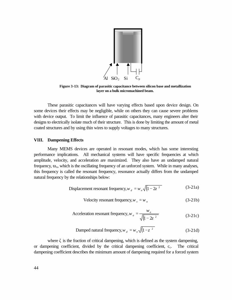
44
These parasitic capacitances will have varying effects based upon device design. Onsome devices their effects may be negligible, while on others they can cause severe problemswith device output. To limit the influence of parasitic capacitances, many engineers alter theirdesigns to electrically isolate much of their structure. This is done by limiting the amount of metalcoated structures and by using thin wires to supply voltages to many structures.
VIII. Dampening Effects
Many MEMS devices are operated in resonant modes, which has some interestingperformance implications. All mechanical systems will have specific frequencies at whichamplitude, velocity, and acceleration are maximized. They also have an undamped naturalfrequency, ωn, which is the oscillating frequency of an unforced system. While in many analyses,this frequency is called the resonant frequency, resonance actually differs from the undampednatural frequency by the relationships below:
Displacement resonant frequency, ( )221 ζωω −= nd
Velocity resonant frequency, nv ωω =
Acceleration resonant frequency,( )221 ζ
ωω
−= n
a
Damped natural frequency, ( )21 ζωω −= nd
where ζ is the fraction of critical dampening, which is defined as the system dampening,or dampening coefficient, divided by the critical dampening coefficient, cc. The criticaldampening coefficient describes the minimum amount of dampening required for a forced system
Al SiO2 Si
Figure 3-13: Diagram of parasitic capacitance between silicon base and metallizationlayer on a bulk micromachined beam.
Cp
(3-21a)
(3-21b)
(3-21c)
(3-21d)
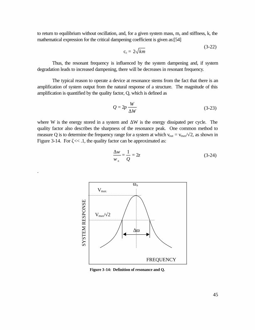
45
to return to equilibrium without oscillation, and, for a given system mass, m, and stiffness, k, themathematical expression for the critical dampening coefficient is given as:[54]
cc = km2
Thus, the resonant frequency is influenced by the system dampening and, if systemdegradation leads to increased dampening, there will be decreases in resonant frequency.
The typical reason to operate a device at resonance stems from the fact that there is anamplification of system output from the natural response of a structure. The magnitude of thisamplification is quantified by the quality factor, Q, which is defined as
WW
Q∆
= π2
where W is the energy stored in a system and ∆W is the energy dissipated per cycle. Thequality factor also describes the sharpness of the resonance peak. One common method tomeasure Q is to determine the frequency range for a system at which vout = vmax/√2, as shown inFigure 3-14. For ζ<< .1, the quality factor can be approximated as:
ζω
ω2
1==
∆Qn
.
Figure 3-14: Definition of resonance and Q.
SYST
EM
RE
SPO
NSE
FREQUENCY
Vmax
Vmax/√2
ωn
∆ω
(3-22)
(3-23)
(3-24)
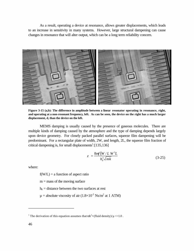
46
As a result, operating a device at resonance, allows greater displacements, which leadsto an increase in sensitivity in many systems. However, large structural dampening can causechanges in resonance that will alter output, which can be a long term reliability concern.
Figure 3-15 (a,b): The difference in amplitude between a linear resonator operating in resonance, right,and operating at a non-resonant frequency, left. As can be seen, the device on the right has a much largerdisplacement, d, than the device on the left.
MEMS damping is usually caused by the presence of gaseous molecules. There aremultiple kinds of damping caused by the atmosphere and the type of damping depends largelyupon device geometry. For closely packed parallel surfaces, squeeze film dampening will bepredominant. For a rectangular plate of width, 2W, and length, 2L, the squeeze film fraction ofcritical dampening is, for small displacements1:[135,136]
( )mkh
LWLWf30
3/8µζ =
where:
f(W/L) = a function of aspect ratio
m = mass of the moving surface
h0 = distance between the two surfaces at rest
µ = absolute viscosity of air (1.8×10⁻⁵ Ns/m2 at 1 ATM)
1 The derivation of this equation assumes that ωh2×(fluid density)/µ <<1.0 .
dd
(3-25)
47
For a device moving in plane, with an area A, and a separation from the substrate, h,there will be a structural dampening factor due to Couette flow of:[24]
mkhA
2µ
ζ =
Since the dampening is proportional to the viscosity of air, which is a function ofpressure, some MEMS utilize vacuum packaging to increase performance. The degree to whicha package holds a seal will determine the operating characteristics of these MEMS. Thuschanges that lead to increased dampening of a system will alter output by shifting resonantfrequency and lowering the quality factor.
IX. Additional Reading
H. G. Van Bueren, Imperfections In Crystals, North-Holland Publishing Company, Amsterdam,1960.
E. Rabinowicz, Friction and Wear of Materials: 2nd Edition, New York, John Wiley & Sons,1995.
A. T. DiBenedetto, The Structure and Properties of Materials, McGraw-Hill, United States ofAmerica, 1967.
(3-26)

48
49
Chapter 4: Material Properties
B. Stark
MEMS are constructed out of a multitude of materials, each of which has uniquereliability implications. Different materials have different responses to failure mechanisms thatneed to be understood to better device reliability. To help clarify the purposes of the myriad ofMEMS materials, this chapter offers a brief overview of the materials used in MEMS andprovides a listing of their properties.
One of the great debates within the MEMS community has focused upon whether touse the thin film or the bulk properties of materials in performing structural analysis. Theproblem with treating many of these materials as bulk materials is that, when samples become assmall as they do in MEMS, crystal defects are no longer small in comparison to the size of thestructure being analyzed. While most testing is performed on macroscopic samples, theseproperties probably do not scale well enough to be used for MEMS, but are often employedanyway for lack of better numbers. For ultimate reliability statistics to be determined, the actualproperties of a given material made on a given process line will have to be characterized.Lacking this, approximations can be made with the available data. This chapter offers thecommon bulk materials properties that are generally accepted. For thin films the applicability ofthese properties is still somewhat in doubt.
I. Single Crystal Silicon
Silicon is the most common material used in semiconductor devices. In crystalline form,silicon aligns in a diamond structure, which consists of a face-centered cubic lattice with a basisof two atoms, as shown in Figure 4-1. The atomic structure of silicon determines many of itsphysical properties, which are listed in Table 4-1.
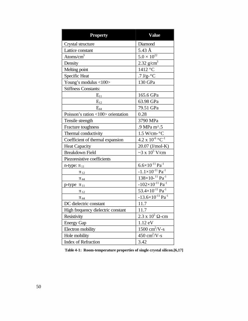
50
Property Value
Crystal structure DiamondLattice constant 5.43 ÅAtoms/cm3 5.0 × 10²²
Density 2.32 g/cm3
Melting point 1412 °CSpecific Heat .7 J/g-°CYoung’s modulus <100> 130 GPaStiffness Constants:
E11 165.6 GPaE12 63.98 GPaE44 79.51 GPa
Poisson’s ration <100> orientation 0.28Tensile strength 3790 MPaFracture toughness .9 MPa m^.5Thermal conductivity 1.5 W/cm-°CCoefficient of thermal expansion 4.2 x 10⁻⁶ °C-1
Heat Capacity 20.07 (J/mol-K)Breakdown Field ~3 x 10⁵ V/cmPiezoresistive coefficientsn-type: π11 6.6×10⁻¹¹ Pa-1
π12 -1.1×10⁻¹¹ Pa-1
π44 138×10-11 Pa-1
p-type π11 -102×10-11 Pa-1
π12 53.4×10⁻¹¹ Pa-1
π44 -13.6×10⁻¹¹ Pa-1
DC dielectric constant 11.7High frequency dielectric constant 11.7Resistivity 2.3 x 10⁵ Ω-cmEnergy Gap 1.12 eVElectron mobility 1500 cm2/V-sHole mobility 450 cm2/V-sIndex of Refraction 3.42
Table 4-1: Room-temperature properties of single crystal silicon.[6,17]

51
As its atomic similarities to diamond might imply, single crystal silicon is a very hardsubstance. It exceeds the mechanical strength of steel, but is decidedly more brittle. Its strengthmakes silicon ideal for many MEMS structures, as it has the highest fracture strength of anymaterial commonly used in MEMS. Due to well controlled processes that yield high puritycrystalline structures, silicon has the desirable quality that its mechanical properties are veryreproducible.[6] For these reasons, silicon is often used for high-quality microstructures.
Figure 4-1: Crystal structure of silicon. (from [96])
The science of silicon growth has developed extensively over the past few years.Silicon wafers are now produced with dislocation densities on the order of .1 dislocations/cm2,which helps to explain the high fracture strength of the material. These wafers also haveimpurity densities less than .03 particles/cm2.
In a diamond cubic lattice, like that of silicon, fracture will normally occur along the111 planes. This is due to the fact that these planes have the lowest surface energy to resistcrack propagation. Although fracture along the other crystal planes is certainly possible, itgenerally will not occur without the aid of a dislocation to lower its strength.[47]
As technology progresses, the fact that silicon does not have the superior electrical andoptical properties of other materials has been a minor drawback. Silicon has a lower electronmobility than some other common semiconductor materials, which impedes high frequencyoperation. While this is a concern for digital designers, it is of little import to MEMS designers,as there are relatively few applications that need mechanical structures to run at the frequencylimits of silicon. On the other hand, the electrical properties of silicon have the advantage that
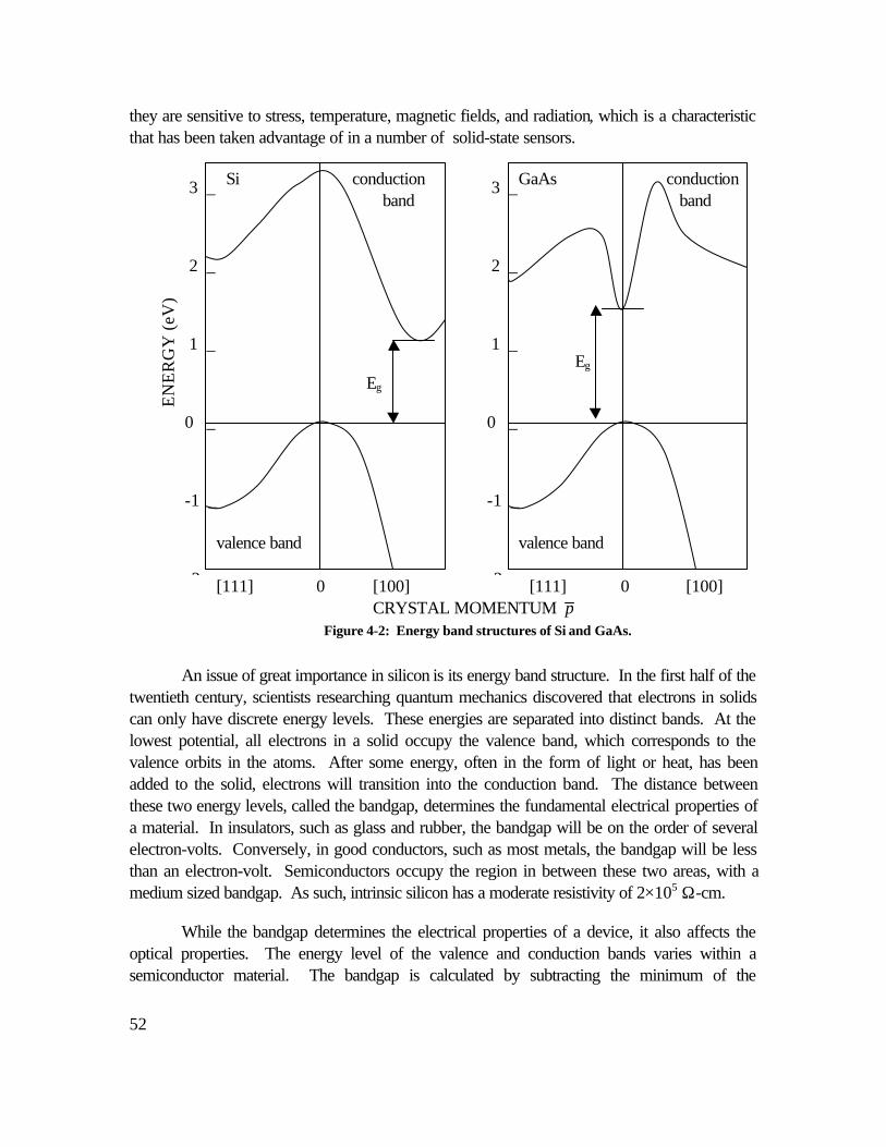
52
they are sensitive to stress, temperature, magnetic fields, and radiation, which is a characteristicthat has been taken advantage of in a number of solid-state sensors.
An issue of great importance in silicon is its energy band structure. In the first half of thetwentieth century, scientists researching quantum mechanics discovered that electrons in solidscan only have discrete energy levels. These energies are separated into distinct bands. At thelowest potential, all electrons in a solid occupy the valence band, which corresponds to thevalence orbits in the atoms. After some energy, often in the form of light or heat, has beenadded to the solid, electrons will transition into the conduction band. The distance betweenthese two energy levels, called the bandgap, determines the fundamental electrical properties ofa material. In insulators, such as glass and rubber, the bandgap will be on the order of severalelectron-volts. Conversely, in good conductors, such as most metals, the bandgap will be lessthan an electron-volt. Semiconductors occupy the region in between these two areas, with amedium sized bandgap. As such, intrinsic silicon has a moderate resistivity of 2×10⁵ Ω-cm.
While the bandgap determines the electrical properties of a device, it also affects theoptical properties. The energy level of the valence and conduction bands varies within asemiconductor material. The bandgap is calculated by subtracting the minimum of the
3 _
2 _
1 _
0 _
-1 _
-2
3 _
2 _
1 _
0 _
-1 _
-2
Si conductionband
valence band
GaAs conduction band
valence band
EN
ER
GY
(eV
)
[111] 0 [100] [111] 0 [100]CRYSTAL MOMENTUM p
Figure 4-2: Energy band structures of Si and GaAs.
Eg
Eg
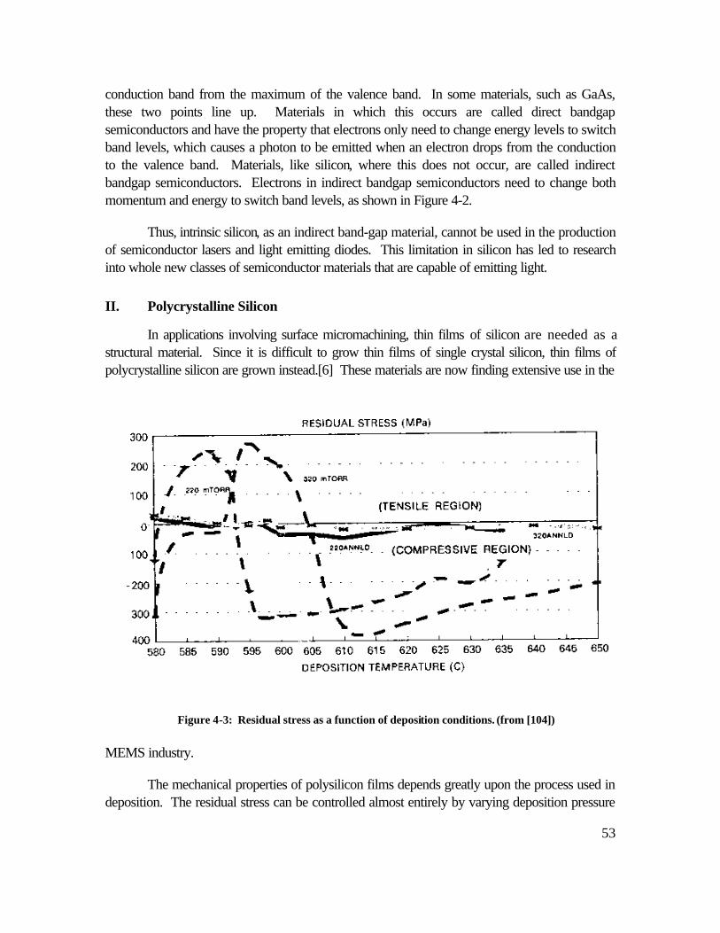
53
conduction band from the maximum of the valence band. In some materials, such as GaAs,these two points line up. Materials in which this occurs are called direct bandgapsemiconductors and have the property that electrons only need to change energy levels to switchband levels, which causes a photon to be emitted when an electron drops from the conductionto the valence band. Materials, like silicon, where this does not occur, are called indirectbandgap semiconductors. Electrons in indirect bandgap semiconductors need to change bothmomentum and energy to switch band levels, as shown in Figure 4-2.
Thus, intrinsic silicon, as an indirect band-gap material, cannot be used in the productionof semiconductor lasers and light emitting diodes. This limitation in silicon has led to researchinto whole new classes of semiconductor materials that are capable of emitting light.
II. Polycrystalline Silicon
In applications involving surface micromachining, thin films of silicon are needed as astructural material. Since it is difficult to grow thin films of single crystal silicon, thin films ofpolycrystalline silicon are grown instead.[6] These materials are now finding extensive use in the
MEMS industry.
The mechanical properties of polysilicon films depends greatly upon the process used indeposition. The residual stress can be controlled almost entirely by varying deposition pressure
Figure 4-3: Residual stress as a function of deposition conditions. (from [104])
54
and temperature, as shown in Figure 4-3. It has also been discovered that there is a direct linkbetween the presence of <110> oriented grains and residual stress in films, although the reasonsfor this are not entirely clear.[45]
The strength of polycrystalline silicon is less well understood. Different researchers havereported a Young’s modulus ranging between 140 to 210 GPa,[130] with these values having adependence on crystal structure and orientation. Recent research has shown that the Young’smodulus of polycrystalline films is highly dependent upon deposition conditions. The filmsexhibit preferential grain orientations that vary with temperature. Since an ideal film does notexhibit orientation dependence for its mechanical properties, researchers have found thatdepositing films at 590 oC, which is the transition point between polycrystalline and amorphoussilicon, is an effective method of producing an isotropic film of polysilicon. At this temperature,the amorphous silicon will recrystalize during annealing, which produces films with a nearlyuniform Young’s modulus of 165 GPa.
In polycrystalline materials, the fracture strength is dependent upon two factors, thegrain size, d, and the fracture surface energy, γs. This stems from the fact that the size of adislocation is usually governed by the grain size, which, by Griffith’s equation, shows that thefracture strength of this material is:[103,119]
dE s
f πγ
σ4
=
As shown by the equation, the fracture strength is also dependent upon the fracturesurface energy, γs. For small grained polycrystals, the energy needed to fracture a grain surfaceincreases with grain size.[44] As a result, larger grains will be stronger due to the increasedenergy needed to propagate a crack across the material.
In several studies, the mean fracture strength of polysilicon has been found to bebetween 2 to 3 GPa, which is clearly less than that of single crystal silicon. Polysilicon fracturesamples have been reported to have a Weibull modulus similar to that of single crystal silicon,which would indicate a similar reliability of the two materials.[40,44,103]
(4-1)
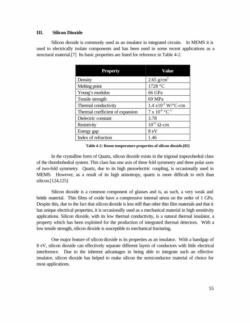
55
III. Silicon Dioxide
Silicon dioxide is commonly used as an insulator in integrated circuits. In MEMS it isused to electrically isolate components and has been used in some recent applications as astructural material.[7] Its basic properties are listed for reference in Table 4-2.
In the crystalline form of Quartz, silicon dioxide exists in the trigonal trapezohedral classof the rhombohedral system. This class has one axis of three fold symmetry and three polar axesof two-fold symmetry. Quartz, due to its high piezoelectric coupling, is occasionally used inMEMS. However, as a result of its high anisotropy, quartz is more difficult to etch thansilicon.[124,125]
Silicon dioxide is a common component of glasses and is, as such, a very weak andbrittle material. Thin films of oxide have a compressive internal stress on the order of 1 GPa.Despite this, due to the fact that silicon dioxide is less stiff than other thin film materials and that ithas unique electrical properties, it is occasionally used as a mechanical material in high sensitivityapplications. Silicon dioxide, with its low thermal conductivity, is a natural thermal insulator, aproperty which has been exploited for the production of integrated thermal detectors. With alow tensile strength, silicon dioxide is susceptible to mechanical fracturing.
One major feature of silicon dioxide is its properties as an insulator. With a bandgap of8 eV, silicon dioxide can effectively separate different layers of conductors with little electricalinterference. Due to the inherent advantages in being able to integrate such an effectiveinsulator, silicon dioxide has helped to make silicon the semiconductor material of choice formost applications.
Property Value
Density 2.65 g/cm3
Melting point 1728 °CYoung’s modulus 66 GPaTensile strength 69 MPaThermal conductivity 1.4 x10⁻² W/°C-cmThermal coefficient of expansion 7 x 10⁻⁶ °C-1
Dielectric constant 3.78Resistivity 1012 Ω-cmEnergy gap 8 eVIndex of refraction 1.46
Table 4-2: Room temperature properties of silicon dioxide.[85]
56
IV. Silicon Carbide
In recent years there has been a growing interest in the use of silicon carbide as amaterial for MEMS. SiC has many properties that make it well suited for MEMS applications,although the SiC wafer growth technology has not matured enough to make it a commonMEMS material. Polycrystalline silicon carbide exists in about 180 different polytypes, with thefour dominant structures listed in Table 4-3.
Modification Polytype
α-SiC 6H(High-temperature modification) 15R
β-SiC4H
(Low-temperature modification) 3C
Table 4-3: Dominant SiC types.[112]
Due to the fact that SiC exists in its beta form at temperatures below 2000 oC, this iscalled its low-temperature modification. Above this temperature, only hexagonal andrhombohedral polytypes are stable.
The properties of SiC are highly dependent upon the processing conditions and can varyquite dramatically. These properties are listed for a few different SiC preparation techniques.
SiC type SiCcontent
Density(g/cm3)
Young’smodulus(GPa)
Thermalexpansioncoefficient(10-6 oC-1)
Thermalconductivity(W /m-K)
Flexuralstrength(MPa)
Ceramicbonded
up to95%
2.55 100 5.8 16 30
Recrystallized 100% 2.55 240 5.0 28 100Sintered 95% 2.55 410 4.9 50 450Hot-pressed 98% 2.55 450 4.5 55 650
Table 4-4: Room temperature properties of SiC.[112]
While not all of these methods are compatible with wafer growth, it should be apparentthat the properties of SiC can vary significantly depending upon processing.
Silicon carbide is used for its extreme hardness and high temperature resistance. SiCdoes not have a defined melting point, instead it has a breakdown point of 2830 oC. At thistemperature, SiC decomposes into graphite and a silicon rich-melt. Many SiC structures are lesselastic than silicon, which is useful in certain MEMS applications. SiC also has a Poisson’s ratiothat varies between .183 and .192. The main drawback to SiC in MEMS has been that the
57
technology used to grow SiC wafers still results in high dislocation densities. This lowers thestrength of SiC, which prohibits its use in many applications. For silicon carbide to findwidespread use, the techniques used to manufacture it must continue to mature.[112,113]
Silicon carbide, with a band-gap around 3eV, is a wide-bandgap semiconductormaterial. While the exact width of the bandgap depends on the polytype, SiC is a better naturalinsulator that Si or GaAs. Intrinsic SiC has a resistivity of 108 Ω-cm, although doping can varythis value from .1 to 1012 Ω-cm. Silicon carbide also oxidizes readily above 600 oC to formsilicon dioxide by the reaction:[112]
2222 COSiOOSiC +→+
V. Silicon Nitride
Silicon nitride is a material that is employed in a variety of applications. Since it doesnot react well with many etching solutions, silicon nitride is often used to prevent impuritydiffusion and ionic contamination. Its basic properties are listed in Table 4-5.
Property Value1
Density 3.1 g/cm-3
Melting point 1900°CYoung’s Modulus 73 GPaFracture strength 460 MPaCoefficient of thermal expansion 3×10⁻⁵ °C-1
Thermal conductivity 0.28 W /cm-°CResistivity 1015Ω-cmDielectric constant 9.4Breakdown field 1×10⁷ V/cmIndex of refraction 2.1Band gap 3.9-4.1 eV
Table 4-5: Room temperature properties of silicon nitride.[18]
The silicon nitride films used in most MEMS devices are amorphous and are usuallyeither sputtered or deposited by CVD. These films are made with the following reaction, whichoccurs between 300-500 mT and 700-900°C.
1 Varies with processing conditions.
(4-2)
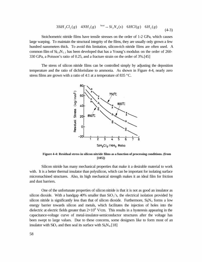
58
)(6)(6)()(4)(3 243322 gHgHClsNSigNHgClSiH heat ++→+
Stoichometric nitride films have tensile stresses on the order of 1-2 GPa, which causeslarge warping. To maintain the structural integrity of the films, they are usually only grown a fewhundred nanometers thick. To avoid this limitation, silicon-rich nitride films are often used. Acommon film of Si1.0N1.1 has been developed that has a Young’s modulus on the order of 260-330 GPa, a Poisson’s ratio of 0.25, and a fracture strain on the order of 3%.[45]
The stress of silicon nitride films can be controlled simply by adjusting the depositiontemperature and the ratio of dichlorisilane to ammonia. As shown in Figure 4-4, nearly zerostress films are grown with a ratio of 4:1 at a temperature of 835 °C.
Figure 4-4: Residual stress in silicon nitride films as a function of processing conditions. (from[105])
Silicon nitride has many mechanical properties that make it a desirable material to workwith. It is a better thermal insulator than polysilicon, which can be important for isolating surfacemicromachined structures. Also, its high mechanical strength makes it an ideal film for frictionand dust barriers.
One of the unfortunate properties of silicon nitride is that it is not as good an insulator assilicon dioxide. With a bandgap 40% smaller than SiO2’s, the electrical isolation provided bysilicon nitride is significantly less than that of silicon dioxide. Furthermore, Si3N4 forms a lowenergy barrier towards silicon and metals, which facilitates the injection of holes into thedielectric at electric fields greater than 2×10⁶ V/cm. This results in a hysteresis appearing in thecapacitance-voltage curve of metal-insulator-semiconductor structures after the voltage hasbeen swept to large values. Due to these concerns, some designers like to form most of aninsulator with SiO2 and then seal its surface with Si3N4.[18]
(4-3)
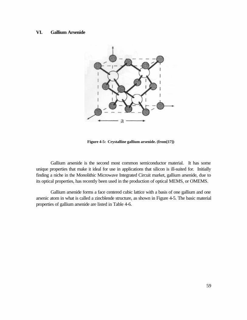
59
VI. Gallium Arsenide
Figure 4-5: Crystalline gallium arsenide. (from[17])
Gallium arsenide is the second most common semiconductor material. It has someunique properties that make it ideal for use in applications that silicon is ill-suited for. Initiallyfinding a niche in the Monolithic Microwave Integrated Circuit market, gallium arsenide, due toits optical properties, has recently been used in the production of optical MEMS, or OMEMS.
Gallium arsenide forms a face centered cubic lattice with a basis of one gallium and onearsenic atom in what is called a zincblende structure, as shown in Figure 4-5. The basic materialproperties of gallium arsenide are listed in Table 4-6.
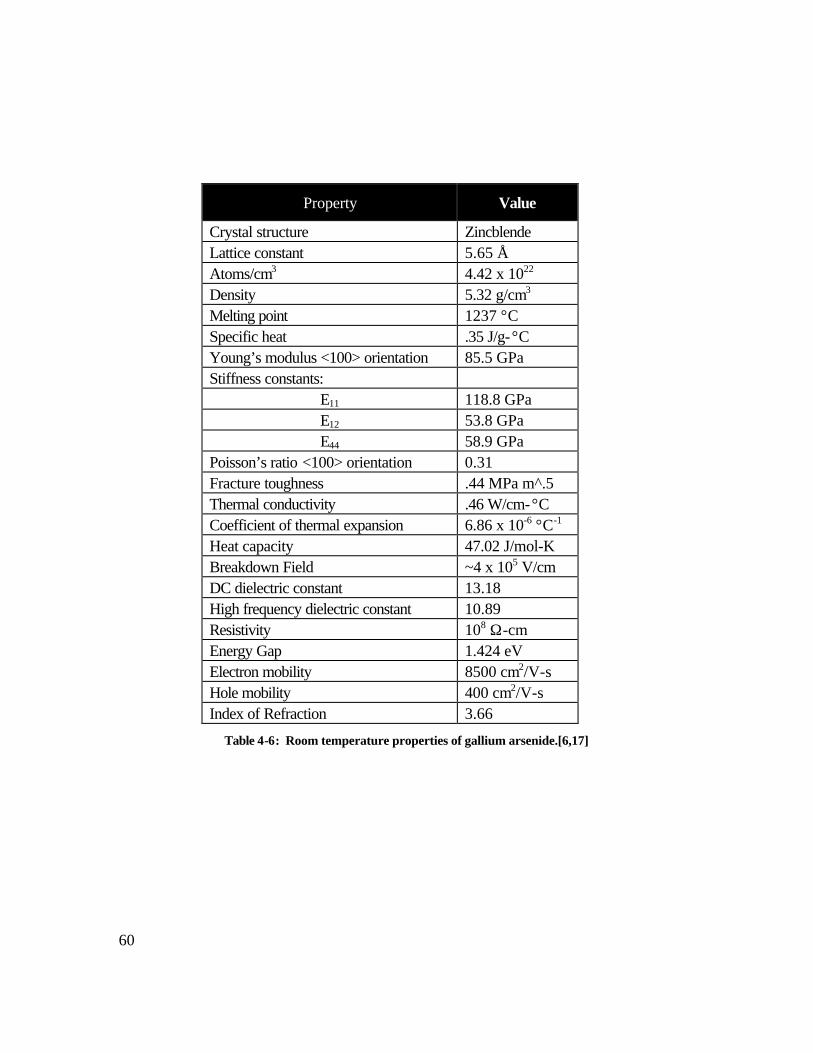
60
Property Value
Crystal structure ZincblendeLattice constant 5.65 ÅAtoms/cm3 4.42 x 10²²
Density 5.32 g/cm3
Melting point 1237 °CSpecific heat .35 J/g-°CYoung’s modulus <100> orientation 85.5 GPaStiffness constants:
E11 118.8 GPaE12 53.8 GPaE44 58.9 GPa
Poisson’s ratio <100> orientation 0.31Fracture toughness .44 MPa m^.5Thermal conductivity .46 W/cm-°CCoefficient of thermal expansion 6.86 x 10⁻⁶ °C-1
Heat capacity 47.02 J/mol-KBreakdown Field ~4 x 10⁵ V/cmDC dielectric constant 13.18High frequency dielectric constant 10.89Resistivity 108 Ω-cmEnergy Gap 1.424 eVElectron mobility 8500 cm2/V-sHole mobility 400 cm2/V-sIndex of Refraction 3.66
Table 4-6: Room temperature properties of gallium arsenide.[6,17]
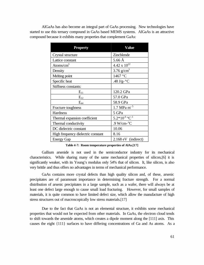
61
AlGaAs has also become an integral part of GaAs processing. New technologies havestarted to use this ternary compound in GaAs based MEMS systems. AlGaAs is an attractivecompound because it exhibits many properties that complement GaAs:
Property Value
Crystal structure ZincblendeLattice constant 5.66 ÅAtoms/cm3 4.42 x 10²²
Density 3.76 g/cm3
Melting point 1467 °CSpecific heat .48 J/g-°CStiffness constants:
E11 120.2 GPaE12 57.0 GPaE44 58.9 GPa
Fracture toughness 1.7 MPa m-.5
Hardness 5 GPaThermal expansion coefficient 5.2*10-6 ºC-1
Thermal conductivity .9 W/cm- oCDC dielectric constant 10.06High frequency dielectric constant 8.16Energy Gap 2.168 eV (indirect)
Table 4-7: Room temperature properties of AlAs.[17]
Gallium arsenide is not used in the semiconductor industry for its mechanicalcharacteristics. While sharing many of the same mechanical properties of silicon,[6] it issignificantly weaker, with its Young’s modulus only 54% that of silicon. It, like silicon, is alsovery brittle and thus offers no advantages in terms of mechanical performance.
GaAs contains more crystal defects than high quality silicon and, of these, arsenicprecipitates are of paramount importance in determining fracture strength. For a normaldistribution of arsenic precipitates in a large sample, such as a wafer, there will always be atleast one defect large enough to cause small load fracturing. However, for small samples ofmaterials, it is quite common to have limited defect size, which allow the manufacture of highstress structures out of macroscopically low stress materials.[17]
Due to the fact that GaAs is not an elemental structure, it exhibits some mechanicalproperties that would not be expected from other materials. In GaAs, the electron cloud tendsto shift towards the arsenide atoms, which creates a dipole moment along the [111] axis. Thiscauses the eight 111 surfaces to have differing concentrations of Ga and As atoms. As a
62
result, the 111 planes are much tougher than expected. This toughening causes the 110planes to be the primary fracture points.[17]
Gallium arsenide also has a thermal conductivity that is less than one-third that of siliconand one-tenth that of copper, which makes it a poor conductor. The consequence of this poorconductivity is that the packing density of GaAs devices is limited by the thermal resistance ofthe substrate. Another thermal concern is the fact that brittle materials becomes ductile ataround 35% of the melting point. Corresponding to 250 °C in GaAs, this marked drop inhardness and increase in fatigue could present serious problems for high temperature deviceoperation.
Gallium arsenide finds most of its applications due to its superior optical and electricalproperties. As shown in Tables 4-1 and 4-6, GaAs has close to six times the electron mobilityof silicon. Electron mobility, which describes how strongly an electron is influenced by anelectric field, is derived from the laws of basic physics and is related to Equation 4-4:
Emqt
v cd
−=*
where:
vd = drift velocity
q = electron charge
tc = mean free times between collisions
m* = effective electron mass
E = electric field
In Equation 4-4, the bracketed proportionality constant is called the electron mobility.As the equation clearly indicates, electron mobility is directly proportionate to the mean free timebetween collisions, tc. This number is in turn a function of the lattice and impurity scattering ofelectrons. The lattice scattering is a result of thermal vibration and increases with temperatureuntil it becomes the dominant factor, as impurity scattering is a constant function of dopinglevels. Thus, the electron mobility is a function of temperature, which changes based on theintensity of device operation. As a result of this, the electron mobility of GaAs is not always sixtimes that of silicon, as it may often only be double that of silicon.[1]
With the electron mobility determining maximum operating frequency and with GaAsalways having a greater electron mobility than silicon, GaAs can operate at higher frequenciesthan silicon, which has made it an ideal material for many communications applications.However, for MEMS, these factors are limited in their import. While some high frequencyGaAs systems are attempting to integrate MEMS components, most GaAs MEMS devices willoperate at significantly lower frequencies due to the mechanical limitations of the systems.
(4-4)
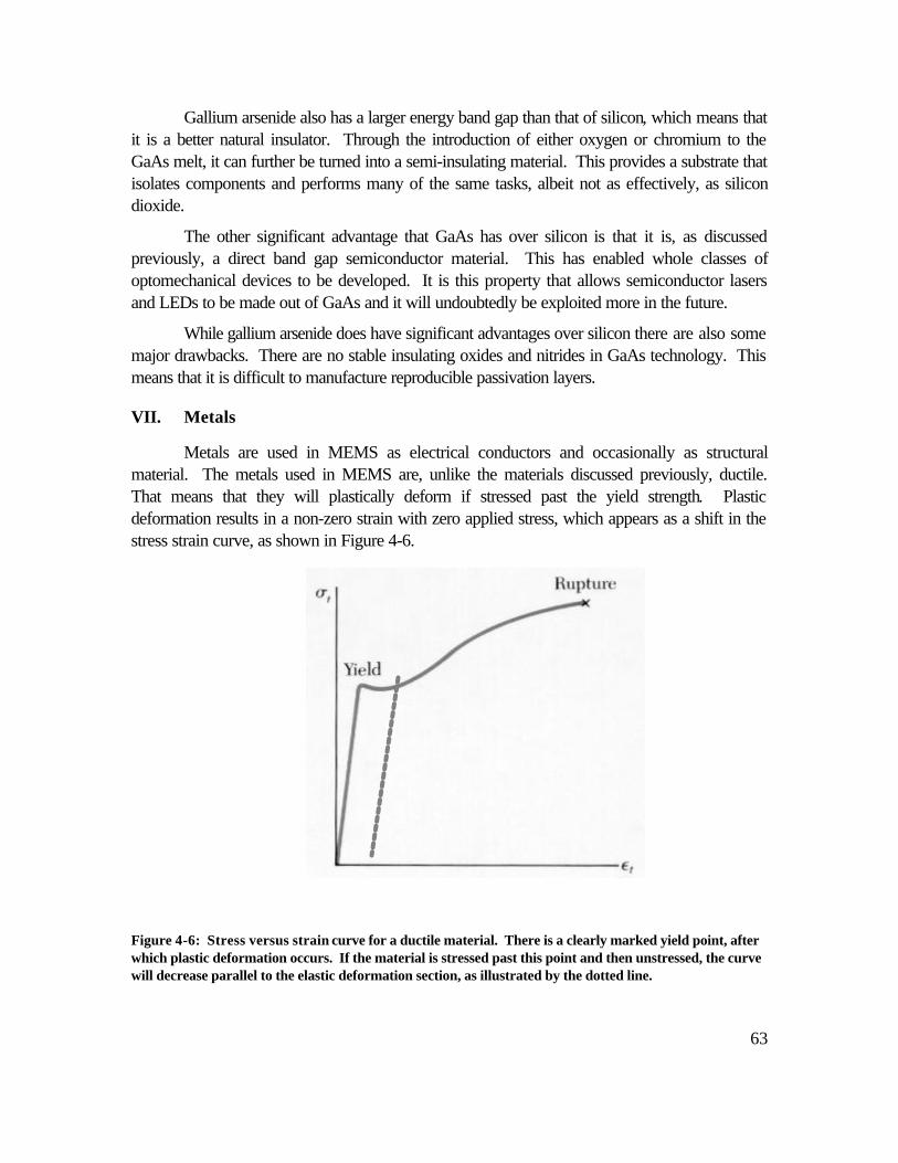
63
Gallium arsenide also has a larger energy band gap than that of silicon, which means thatit is a better natural insulator. Through the introduction of either oxygen or chromium to theGaAs melt, it can further be turned into a semi-insulating material. This provides a substrate thatisolates components and performs many of the same tasks, albeit not as effectively, as silicondioxide.
The other significant advantage that GaAs has over silicon is that it is, as discussedpreviously, a direct band gap semiconductor material. This has enabled whole classes ofoptomechanical devices to be developed. It is this property that allows semiconductor lasersand LEDs to be made out of GaAs and it will undoubtedly be exploited more in the future.
While gallium arsenide does have significant advantages over silicon there are also somemajor drawbacks. There are no stable insulating oxides and nitrides in GaAs technology. Thismeans that it is difficult to manufacture reproducible passivation layers.
VII. Metals
Metals are used in MEMS as electrical conductors and occasionally as structuralmaterial. The metals used in MEMS are, unlike the materials discussed previously, ductile.That means that they will plastically deform if stressed past the yield strength. Plasticdeformation results in a non-zero strain with zero applied stress, which appears as a shift in thestress strain curve, as shown in Figure 4-6.
Figure 4-6: Stress versus strain curve for a ductile material. There is a clearly marked yield point, afterwhich plastic deformation occurs. If the material is stressed past this point and then unstressed, the curvewill decrease parallel to the elastic deformation section, as illustrated by the dotted line.

64
A. Aluminum
Aluminum is commonly used in MEMS as a sputtered film placed over a processedstructure. By covering a structure with a conductive film, equipotential surfaces are created on adevice, which are critical to the operation of many electrostatic device. Aluminum is alsocommonly used as an electrical conductor in semiconductor technologies.
Aluminum, like most metals, is often alloyed with other substances to improve itsstructural properties. The alloys of aluminum are numerous and are offered in great detail inReference [111]. Pure aluminum has many properties that distinguish it from other materialsused in MEMS. Listed in Table 4-8, the properties of aluminum have been both a boon and anarea of concern for researchers over the past decades.
Property Value
Density 2.71 g/m3
Melting Point 659oCSpecific Heat 0.90 J/g- oCYoung’s modulus (bulk value) 70 GPaPoisson’s ratio .35Ultimate tensile strength 110 MPaUltimate shear strength 70 MPaYield tensile strength 100 MPaYield shear strength 55 MPaThermal conductivity 2.37 W/cm- oCCoefficient of thermal expansion 23.6×10⁻⁶ oC-1
Resistivity 2.82×10⁻⁶ Ω-cm
Table 4-8: Room temperature properties of 99.6% pure aluminum.[46,101,111]
The mechanical properties of aluminum are considerably poorer than Si and GaAs.With a Young’s modulus that is less than half that of silicon, it is clearly a more ductile material.However, since the yield strength of aluminum, at 100 MPa, is at least an order of magnitudebelow the fracture strength of Si and GaAs, aluminum is rarely used as a structural support inMEMS.
For a considerable amount of time, aluminum was the only good conductor that couldeasily be integrated into ICs. Since aluminum forms Al2O3 bonds with SiO2, it is simple toadhere it to passivation layers. This fact lead to its widespread implementation, despite the factthat materials existed with better electrical properties.
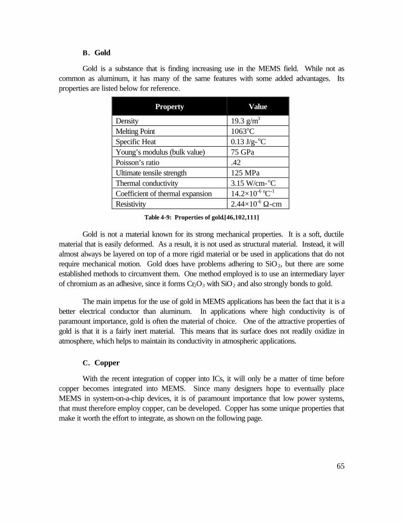
65
B. Gold
Gold is a substance that is finding increasing use in the MEMS field. While not ascommon as aluminum, it has many of the same features with some added advantages. Itsproperties are listed below for reference.
Property Value
Density 19.3 g/m3
Melting Point 1063oCSpecific Heat 0.13 J/g- oCYoung’s modulus (bulk value) 75 GPaPoisson’s ratio .42Ultimate tensile strength 125 MPaThermal conductivity 3.15 W/cm- oCCoefficient of thermal expansion 14.2×10⁻⁶ oC-1
Resistivity 2.44×10⁻⁶ Ω-cm
Table 4-9: Properties of gold.[46,102,111]
Gold is not a material known for its strong mechanical properties. It is a soft, ductilematerial that is easily deformed. As a result, it is not used as structural material. Instead, it willalmost always be layered on top of a more rigid material or be used in applications that do notrequire mechanical motion. Gold does have problems adhering to SiO2, but there are someestablished methods to circumvent them. One method employed is to use an intermediary layerof chromium as an adhesive, since it forms Cr2O3 with SiO2 and also strongly bonds to gold.
The main impetus for the use of gold in MEMS applications has been the fact that it is abetter electrical conductor than aluminum. In applications where high conductivity is ofparamount importance, gold is often the material of choice. One of the attractive properties ofgold is that it is a fairly inert material. This means that its surface does not readily oxidize inatmosphere, which helps to maintain its conductivity in atmospheric applications.
C. Copper
With the recent integration of copper into ICs, it will only be a matter of time beforecopper becomes integrated into MEMS. Since many designers hope to eventually placeMEMS in system-on-a-chip devices, it is of paramount importance that low power systems,that must therefore employ copper, can be developed. Copper has some unique properties thatmake it worth the effort to integrate, as shown on the following page.
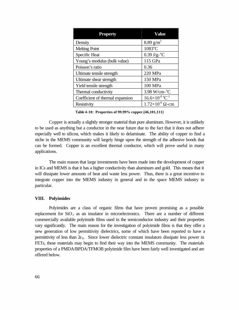
66
Property Value
Density 8.89 g/m3
Melting Point 1083oCSpecific Heat 0.39 J/g- oCYoung’s modulus (bulk value) 115 GPaPoisson’s ratio 0.36Ultimate tensile strength 220 MPaUltimate shear strength 150 MPaYield tensile strength 100 MPaThermal conductivity 3.98 W/cm- oCCoefficient of thermal expansion 16.6×10⁻⁶ oC-1
Resistivity 1.72×10⁻⁶ Ω-cm
Table 4-10: Properties of 99.99% copper.[46,101,111]
Copper is actually a slightly stronger material than pure aluminum. However, it is unlikelyto be used as anything but a conductor in the near future due to the fact that it does not adhereespecially well to silicon, which makes it likely to delaminate. The ability of copper to find aniche in the MEMS community will largely hinge upon the strength of the adhesive bonds thatcan be formed. Copper is an excellent thermal conductor, which will prove useful in manyapplications.
The main reason that large investments have been made into the development of copperin ICs and MEMS is that it has a higher conductivity than aluminum and gold. This means that itwill dissipate lower amounts of heat and waste less power. Thus, there is a great incentive tointegrate copper into the MEMS industry in general and in the space MEMS industry inparticular.
VIII. Polyimides
Polyimides are a class of organic films that have proven promising as a possiblereplacement for SiO2 as an insulator in microelectronics. There are a number of differentcommercially available polyimide films used in the semiconductor industry and their propertiesvary significantly. The main reason for the investigation of polyimide films is that they offer anew generation of low permittivity dielectrics, some of which have been reported to have apermittivity of less than 2ε0. Since lower dielectric constant insulators dissipate less power inFETs, these materials may begin to find their way into the MEMS community. The materialsproperties of a PMDA/BPDA/TFMOB polyimide film have been fairly well investigated and areoffered below.
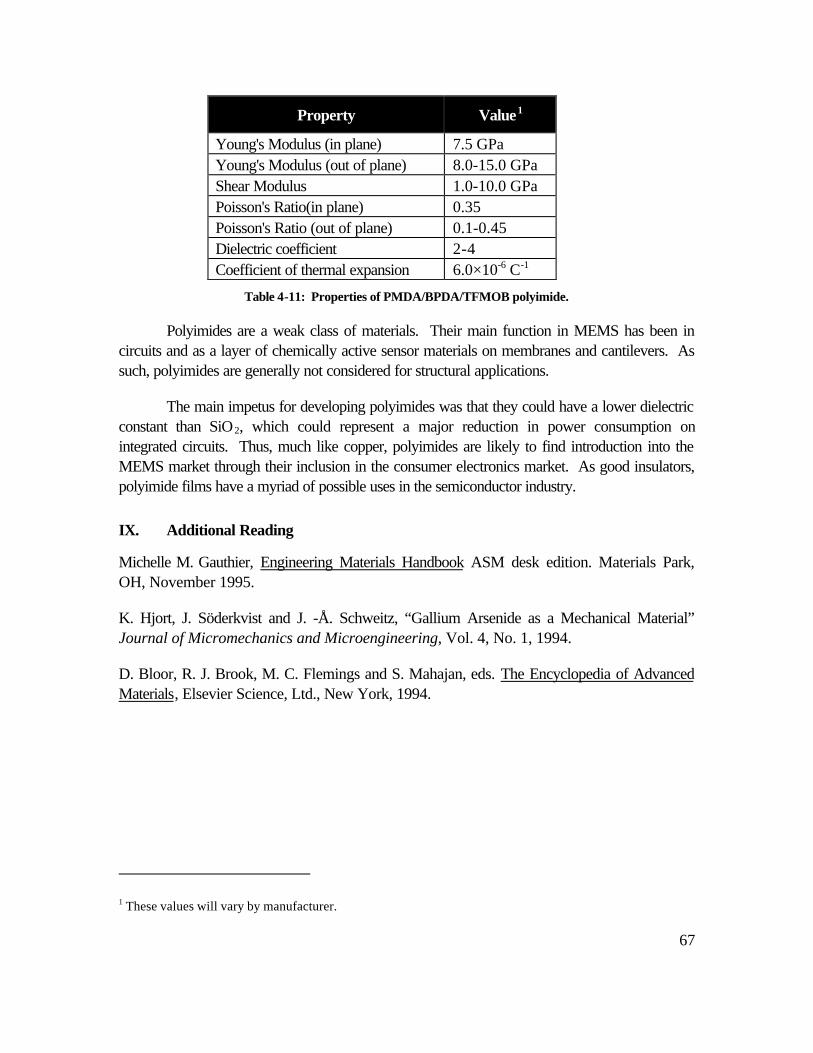
67
Property Value1
Young's Modulus (in plane) 7.5 GPaYoung's Modulus (out of plane) 8.0-15.0 GPaShear Modulus 1.0-10.0 GPaPoisson's Ratio(in plane) 0.35Poisson's Ratio (out of plane) 0.1-0.45Dielectric coefficient 2-4Coefficient of thermal expansion 6.0×10⁻⁶ C-1
Table 4-11: Properties of PMDA/BPDA/TFMOB polyimide.
Polyimides are a weak class of materials. Their main function in MEMS has been incircuits and as a layer of chemically active sensor materials on membranes and cantilevers. Assuch, polyimides are generally not considered for structural applications.
The main impetus for developing polyimides was that they could have a lower dielectricconstant than SiO2, which could represent a major reduction in power consumption onintegrated circuits. Thus, much like copper, polyimides are likely to find introduction into theMEMS market through their inclusion in the consumer electronics market. As good insulators,polyimide films have a myriad of possible uses in the semiconductor industry.
IX. Additional Reading
Michelle M. Gauthier, Engineering Materials Handbook ASM desk edition. Materials Park,OH, November 1995.
K. Hjort, J. Söderkvist and J. -Å. Schweitz, “Gallium Arsenide as a Mechanical Material”Journal of Micromechanics and Microengineering, Vol. 4, No. 1, 1994.
D. Bloor, R. J. Brook, M. C. Flemings and S. Mahajan, eds. The Encyclopedia of AdvancedMaterials, Elsevier Science, Ltd., New York, 1994.
1 These values will vary by manufacturer.

68
69
Chapter 5: MEMS Device Processing
B. Stark and W. C. Tang
The growth of MEMS has largely been due to innovations in processing technologies.Adaptations in the processes used to manufacture integrated circuits have led to thedevelopment of MEMS and will continue to define the dimensional limitations in devices. It isultimately these technologies that determine the specifications and reliability characteristics of anygiven device. As such, they are critically important to understanding MEMS. This chapteroffers a brief overview of the most common processing techniques used today. It thendescribes the integration of these techniques into micromachining.
In the fabrication of common MEMS devices, there are two basic techniques employed.Devices can be constructed by patterning the bulk material of a wafer into a desired structureor, alternatively, by patterning thin films of material deposited on the surface of a wafer. Thesetwo processes, respectively called bulk and surface micromachining, are the basis for anyMEMS fabrication technology.
I. Microfabrication Processing Steps
There is a variety of processing techniques that are often used in all MEMSprocesses.[6] The degree to which they are successfully implemented in any given technologydetermines the viability of the technology. They are listed below to give a basic description ofMEMS processing.
A. Thin Film Growth and Deposition
Thin films are an essential building block of semiconductor devices. Surfacemicromachined devices are constructed entirely out of successive layers of thin films and bulkmicromachined devices that employ thin films of silicon dioxide for electrical isolation. There areseveral common methods for placing thin films on MEMS that are discussed in this section.
i) Spin Casting
In this process, a material is in a solution with a volatile liquid solvent. The solution ispoured onto a wafer, which is rotated at high speed. As the liquid spreads over the surface ofthe wafer, the solvent evaporates, leaving behind a thin film of the solid material, which can beanywhere from .1 to 50 µm thick. Spin casting is useful for depositing organic materials, such asphotoresist, as well as inorganic glasses. Spin casting blurs the underlying topography of a
70
structure, yielding a smooth surface. Spun cast materials are susceptible to severe shrinkagewhenever the film coalesces, either from solvent removal or post-bake. This means that spincast films have an inherently high residual stress. Spin cast films are also less dense and moresusceptible to chemical attack than materials deposited by other means.[6]
ii) Evaporation
Another way to place a material in a thin film on a wafer is to evaporate them from a hotsource. The evaporation system uses a vacuum chamber, which is pumped down from 10-6 to10-7 Torr. A crucible is then heated to flash-evaporate material onto a sample. This process iscontrolled by a shutter, which limits the amount of time in which the wafer is exposed to thecrucible. The thickness of the film is governed by the length of time that the shutter is open andis also a function of the vapor pressure of the material. Thus materials with a high melting point,such as tungsten, require high temperatures to evaporate, which can burn organic films that areon the wafer. Since evaporated films originate from a point source and the vaporized materialstravel in a straight path, they suffer from shadowing effects that yield non-uniform thickness andpoor step coverage.[6] A second factor affecting the coverage is the surface mobility of thespecies on the substrate. As a general rule, evaporated films are highly disordered, whichcauses a large residual stress and limits the thickness of the films.
RoughingPump
VacuumChamber
Wafers
Charge
Crucible
Vent gas
Cold trap
DiffusionPump
BackingPump
Figure 5-1: A typical evaporation system. (after [46])
71
iii) Sputtering
Sputtering is a thin film growth technique that eliminates many of the problems inherentto flash-evaporation. Sputtering works by inserting a wafer into a vacuum chamber that issubsequently pumped down to between 10-6 and 10-8 Torr. Then an inert gas of a few mTorr ofpressure is introduced into the system, which is then ignited into a plasma. The highly energeticions of the plasma strike a target of sample material and tear atoms off its surface. These atomsthen form a thin film across the wafer. This process creates a continuous planar flux of thespecies landing on the wafer, which makes preferable for mass production.[6] Anotherdesirable aspect of sputtering is that the high energy plasma does not have the same temperatureproblems inherent to evaporation. Most elements and many inorganic and organic compoundscan be sputtered. Refractory materials that are difficult to evaporate can be easily sputtered aswell. Sputtering can also be done with more than one target, which allows control of the atomiccomposition of thin film alloys. Sputtered films have better step coverage and uniformity thanevaporated films, but they are disorganized structures whose mechanical properties and residualstresses are sensitive to sputtering conditions. Problems also arise from the inert gas used in thesputtering process, which can become trapped in the film and cause inconsistencies in themechanical properties of the films.[46]
Figure 5-2: Basic sputtering system. (from [46])
72
iv) Reactive Growth
Reactive growth differs from the previously mentioned methods in that it utilizes chemicalreactions with the substrate to construct thin films on wafers. The most common example of thisprocess is with the growth of oxide films on silicon wafers. In this process, a wafer is placedinto a furnace with oxygen gas (dry oxidation) or steam (wet oxidation). The silicon is graduallyoxidized at a highly predictable rate that depends upon temperature and crystalline orientation.
.
Reactively grown films are usually of excellent quality but suffer from large residualstresses due to volume changes in the processed sample. In silicon dioxide growth, there is avolume change of about 45%, which causes mechanical warping.
concentrationgradient
O2 SiO 2 Si Wafer
reaction of O2 and Si atSiO2/Si interface
Figure 5-3: Reactive growth process.
73
v) Chemical Vapor Deposition
Chemical vapor deposition, or CVD, involves thermally breaking down gaseouscompounds into their components. When they impact a wafer, some of these componentsnucleate onto it, which grows a thin film. CVD is limited by both the mass transport andreaction-limited processes, with the latter method being preferable due to its better uniformity.This process can be used to deposit many common semiconductor materials, including silicondioxide, silicon nitride, polycrystalline silicon, and refractory metals. In low pressure thermalCVD, or LPCVD, films with the most desirable mechanical properties are produced. Unlikeother methods, CVD films can be deposited conformally on a sample. This property allowsCVD films to seal cavities, which can be advantageous in many devices. The stresses andmechanical properties of CVD films can be controlled through the deposition conditions andsubsequent annealing. A CVD process called epitaxial growth can be utilized to grow singlecrystal films on crystalline substrates. Since these films have the same properties as bulkcrystals, they could find a multitude of applications in the MEMS industry.
Figure 5-4: A chemical vapor deposition system. (from [179])
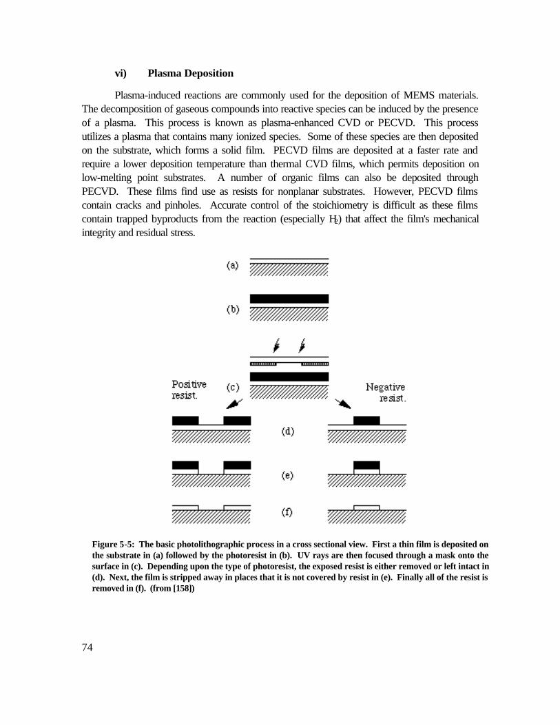
74
vi) Plasma Deposition
Plasma-induced reactions are commonly used for the deposition of MEMS materials.The decomposition of gaseous compounds into reactive species can be induced by the presenceof a plasma. This process is known as plasma-enhanced CVD or PECVD. This processutilizes a plasma that contains many ionized species. Some of these species are then depositedon the substrate, which forms a solid film. PECVD films are deposited at a faster rate andrequire a lower deposition temperature than thermal CVD films, which permits deposition onlow-melting point substrates. A number of organic films can also be deposited throughPECVD. These films find use as resists for nonplanar substrates. However, PECVD filmscontain cracks and pinholes. Accurate control of the stoichiometry is difficult as these filmscontain trapped byproducts from the reaction (especially H2) that affect the film's mechanicalintegrity and residual stress.
Figure 5-5: The basic photolithographic process in a cross sectional view. First a thin film is deposited onthe substrate in (a) followed by the photoresist in (b). UV rays are then focused through a mask onto thesurface in (c). Depending upon the type of photoresist, the exposed resist is either removed or left intact in(d). Next, the film is stripped away in places that it is not covered by resist in (e). Finally all of the resist isremoved in (f). (from [158])
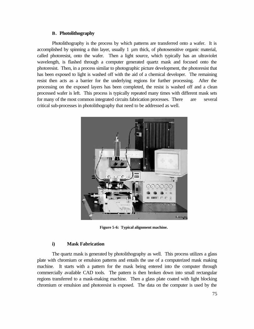
75
B. Photolithography
Photolithography is the process by which patterns are transferred onto a wafer. It isaccomplished by spinning a thin layer, usually 1 µm thick, of photosensitive organic material,called photoresist, onto the wafer. Then a light source, which typically has an ultravioletwavelength, is flashed through a computer generated quartz mask and focused onto thephotoresist. Then, in a process similar to photographic picture development, the photoresist thathas been exposed to light is washed off with the aid of a chemical developer. The remainingresist then acts as a barrier for the underlying regions for further processing. After theprocessing on the exposed layers has been completed, the resist is washed off and a cleanprocessed wafer is left. This process is typically repeated many times with different mask setsfor many of the most common integrated circuits fabrication processes. There are severalcritical sub-processes in photolithography that need to be addressed as well.
i) Mask Fabrication
The quartz mask is generated by photolithography as well. This process utilizes a glassplate with chromium or emulsion patterns and entails the use of a computerized mask makingmachine. It starts with a pattern for the mask being entered into the computer throughcommercially available CAD tools. The pattern is then broken down into small rectangularregions transferred to a mask-making machine. Then a glass plate coated with light blockingchromium or emulsion and photoresist is exposed. The data on the computer is used by the
Figure 5-6: Typical alignment machine.
76
mask maker to position the mask and determine the size of a variable aperture shutter on theultraviolet light source. Each of the rectangular boxes is then individually exposed onto the plate.Depending upon the design, this process may be repeated over one hundred thousand timesbefore the mask is finished. After this exposure step, the photoresist is developed and thechromium or emulsion patterns are etched.
ii) Alignment and Exposure
In processes that require multiple masks, each mask layer must perfectly match thefeatures on the substrate. This is done by aligning the mask to special features, called alignmentkeys, on the wafer prior to exposure. A typical mechanical alignment utilizes a sample, maskholder, a stereoscopic microscope, an ultraviolet light source, and a precision positioning stage,as shown in Figure 5-6. This can either be done with a stepper aligner, which exposes one dieat a time, or with a contact aligner, which exposes the whole wafer at once. Often in MEMS,the fabrication process requires photolithography to be performed on both sides of a wafer. Toaccomplish this, two masks are aligned with each other inside a secure assembly. Then thewafer is inserted and aligned with one of the two masks before being exposed to the ultravioletlight source. There is also an alternative method employed that uses an infrared microscope tolocate alignment keys on the back-side, which could offer better alignment precision.[6]
C. Etching and Patterning Techniques
After a pattern has been transferred onto a wafer, it is often necessary to strip awayunwanted sections of materials. This process, called etching, determines the dimensions of aMEMS structure. Invariably the reliability of a device will be related to how well the etching isperformed and, as such, it must be well understood before a device can be qualified. There areseveral standard etching techniques used throughout MEMS processing that will be discussed inthe following sections.
i) Lift-off
Lift-off is a simple patterning technique. It is accomplished by depositing a layer ofsacrificial material, like photoresist, on a substrate. This layer is then patterned, which usuallyinvolves the photolithographic processes discussed above. Then a layer of structural film isevaporated onto the substrate. The pattern on the sacrificial layer is then transferred to thestructural layer by removing the sacrificial layer. This has the effect of removing all of thestructural material that is on top of the sacrificial layer, thus leaving a patterned structural film.
ii) Wet Etching
Wet etching involves immersing a wafer patterned with photoresist or other etch masksin a chemical bath. The chemical etchant selectively removes material not covered with the
77
mask. The exact profile of the patterning depend on the anisotropy of the etch. Wet etchantsall exhibit a degree of isotropic behavior. This has the effect of undercutting the patternedstructure, making it smaller than the resist mask. The degree to which the etchants etch the<100>:<110>:<111> directions is responsible for determining the maximum aspect ratio ofmany structures. Another important aspect of many etchants is their ability to selectively etchone material over the other. Called selectivity, this ratio determines how thick etch stops mustbe and provides dimensional limits on many technologies.
There are several different chemicals used in wet etching. Acidic etches are used forisotropic release etches. These are usually completely isotropic etches that are designed toseparate suspended structures from the underlying substrate. Common acidic etchants are HF,HNO3, and CH3COOH. These chemicals etch from 50 to 150 µm/h. SiO2 is often used as anetch stop for these materials, as it is usually etched at a rate of 2 µm/h.
For an anisotropic etch, alkaline etchants are commonly used. These exhibit differentdegrees of selectivity and etch rates. Typically these chemicals etch <111> planes much slowerthan the <100> and <110> planes. This effect and its impact upon MEMS devices is discussedin greater detail in Section 5-IIA. Some etchants can also be influenced by the introduction ofboron into the bulk material, which can greatly reduce the etch rate. It is also possible toinfluence etch rates in a process known as electrochemical etching, which involves applying avoltage across a p-n junction.
iii) Dry Etching
Dry etching, also referred to as reactive ion etching, or RIE, involves using etchants in agaseous state. The etchant is converted to a highly ionized plasma. Dry etching is performed ina chamber pumped down to a pressure between 10 mTorr and 1 Torr. A wafer is placedbetween two electrodes, which are then exposed to an RF voltage, which creates a plasma inthe chamber. Etching occurs when highly reactive free radicals in the plasma react with thesolid-phase material of the film. The anisotropy of the etch is a result of the chemical reactionbeing preferentially enhanced on the side of the wafer parallel to the electrodes by bombardmentfrom ions in the plasma. The ions impinge the surface of a film and expose underlying material,which is then etched away by the gas. The ions accelerate the etching process considerably,which means that the vertical sidewalls of the wafer, which do not interact with the ions, are notaffected by dry etching.
GaAs anisotropic etching is usually performed in chlorinated gasses. One of theproblems with GaAs etching is that, due to differences in the etch rates of group III and group Vhalides, the speed of etching in GaAs varies with crystal planes. In low power, high pressureCl2 gasses, significant faceting can occur. There are several methods that can be used to avoidthis problem. It is possible to add certain compounds to form polymers in the plasma andpassivate the side walls, thus preventing the problem. Another possibility is to use hydrides to
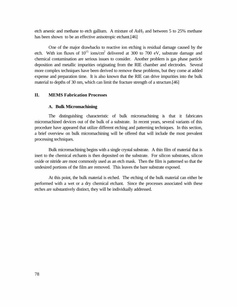
78
etch arsenic and methane to etch gallium. A mixture of AsH3 and between 5 to 25% methanehas been shown to be an effective anisotropic etchant.[46]
One of the major drawbacks to reactive ion etching is residual damage caused by theetch. With ion fluxes of 1015 ions/cm2 delivered at 300 to 700 eV, substrate damage andchemical contamination are serious issues to consider. Another problem is gas phase particledeposition and metallic impurities originating from the RIE chamber and electrodes. Severalmore complex techniques have been derived to remove these problems, but they come at addedexpense and preparation time. It is also known that the RIE can drive impurities into the bulkmaterial to depths of 30 nm, which can limit the fracture strength of a structure.[46]
II. MEMS Fabrication Processes
A. Bulk Micromachining
The distinguishing characteristic of bulk micromachining is that it fabricatesmicromachined devices out of the bulk of a substrate. In recent years, several variants of thisprocedure have appeared that utilize different etching and patterning techniques. In this section,a brief overview on bulk micromachining will be offered that will include the most prevalentprocessing techniques.
Bulk micromachining begins with a single crystal substrate. A thin film of material that isinert to the chemical etchants is then deposited on the substrate. For silicon substrates, siliconoxide or nitride are most commonly used as an etch mask. Then the film is patterned so that theundesired portions of the film are removed. This leaves the bare substrate exposed.
At this point, the bulk material is etched. The etching of the bulk material can either beperformed with a wet or a dry chemical etchant. Since the processes associated with theseetches are substantively distinct, they will be individually addressed.
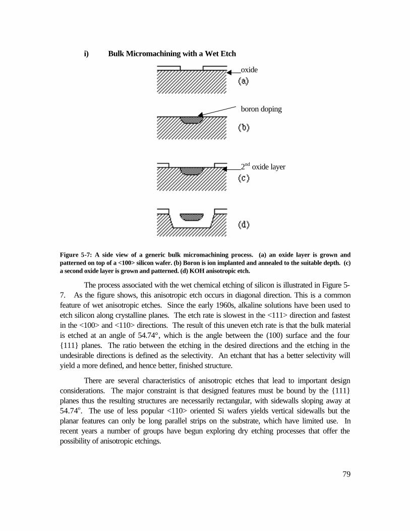
79
i) Bulk Micromachining with a Wet Etch
Figure 5-7: A side view of a generic bulk micromachining process. (a) an oxide layer is grown andpatterned on top of a <100> silicon wafer. (b) Boron is ion implanted and annealed to the suitable depth. (c)a second oxide layer is grown and patterned. (d) KOH anisotropic etch.
The process associated with the wet chemical etching of silicon is illustrated in Figure 5-7. As the figure shows, this anisotropic etch occurs in diagonal direction. This is a commonfeature of wet anisotropic etches. Since the early 1960s, alkaline solutions have been used toetch silicon along crystalline planes. The etch rate is slowest in the <111> direction and fastestin the <100> and <110> directions. The result of this uneven etch rate is that the bulk materialis etched at an angle of 54.74°, which is the angle between the (100) surface and the four111 planes. The ratio between the etching in the desired directions and the etching in theundesirable directions is defined as the selectivity. An etchant that has a better selectivity willyield a more defined, and hence better, finished structure.
There are several characteristics of anisotropic etches that lead to important designconsiderations. The major constraint is that designed features must be bound by the 111planes thus the resulting structures are necessarily rectangular, with sidewalls sloping away at54.74o. The use of less popular <110> oriented Si wafers yields vertical sidewalls but theplanar features can only be long parallel strips on the substrate, which have limited use. Inrecent years a number of groups have begun exploring dry etching processes that offer thepossibility of anisotropic etchings.
oxide
boron doping
2nd oxide layer
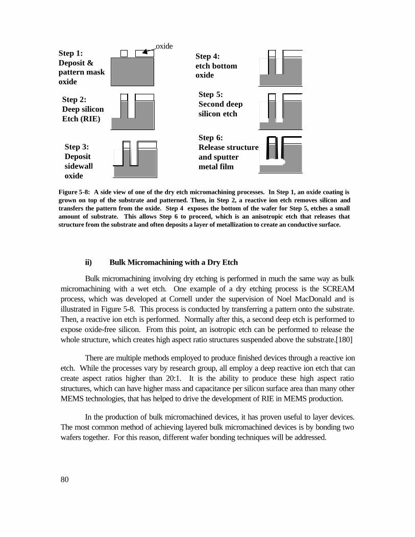
80
ii) Bulk Micromachining with a Dry Etch
Bulk micromachining involving dry etching is performed in much the same way as bulkmicromachining with a wet etch. One example of a dry etching process is the SCREAMprocess, which was developed at Cornell under the supervision of Noel MacDonald and isillustrated in Figure 5-8. This process is conducted by transferring a pattern onto the substrate.Then, a reactive ion etch is performed. Normally after this, a second deep etch is performed toexpose oxide-free silicon. From this point, an isotropic etch can be performed to release thewhole structure, which creates high aspect ratio structures suspended above the substrate.[180]
There are multiple methods employed to produce finished devices through a reactive ionetch. While the processes vary by research group, all employ a deep reactive ion etch that cancreate aspect ratios higher than 20:1. It is the ability to produce these high aspect ratiostructures, which can have higher mass and capacitance per silicon surface area than many otherMEMS technologies, that has helped to drive the development of RIE in MEMS production.
In the production of bulk micromachined devices, it has proven useful to layer devices.The most common method of achieving layered bulk micromachined devices is by bonding twowafers together. For this reason, different wafer bonding techniques will be addressed.
Step 3:Depositsidewalloxide
Step 5:Second deepsilicon etch
Step 6:Release structureand sputtermetal film
Step 1:Deposit &pattern maskoxide
Step 2:Deep siliconEtch (RIE)
Step 4:etch bottomoxide
Figure 5-8: A side view of one of the dry etch micromachining processes. In Step 1, an oxide coating isgrown on top of the substrate and patterned. Then, in Step 2, a reactive ion etch removes silicon andtransfers the pattern from the oxide. Step 4 exposes the bottom of the wafer for Step 5, etches a smallamount of substrate. This allows Step 6 to proceed, which is an anisotropic etch that releases thatstructure from the substrate and often deposits a layer of metallization to create an conductive surface.
oxide
81
iii) Wafer Bonding
Wafer bonding has been used in recent years for both sealing microsensors and for theconstruction of composite sensors. There are several kinds of wafer bonding techniquescommonly employed, which are discussed below.
(1) Anodic Bonding
Anodic, or electrostatic, bonding is a process that bonds a conductive substrate, whichis usually silicon, to a sodium rich glass substrate. This is done by putting the two substrates intodirect contact. They are then heated to between 350-400 °C, which mobilizes the sodium ionsin the glass. Then a voltage of 400-700 V is applied between the two substrates, with the glasssubstrate being made negative with respect to the silicon wafer. This repels the sodium ionsfrom the interface and creates an ion-depletion region about a micron thick with electric fields onthe order of 7×10⁶ V/m. This creates an electrostatic pressure of several atmospheres, whichpulls the two wafers together while a thin layer of SiO2 is formed. The end result of this processis a hermetically sealed bond with a strength that exceeds that of the individual substrates.
There are several reliability concerns in producing these bonds. The high temperature atwhich the bond is formed can induce thermal mismatch warping in a processed device. Therecan also be warping at the bonding interface from unmatched thermal coefficients of expansion.Currently, Corning glass 7740 offers the closest match to silicon. Another concern is theintroduction of the large voltages and electric fields inherent to the bonding process. It ispossible to destroy the device in the bonding process if these factors are not considered.[6]
(2) Low-Temperature Glass Bonding
Low-temperature glass bonding offers a viable alternative to anodic bonding forapplications where high voltages are unacceptable. In this process, the bonding interface iscovered with a thin film of low-temperature glass. The wafers are then placed into contactunder pressure and heated to create the bond. The low-temperature glass then either melts orcrystallizes, depending upon the actual glass used, which bonds the two substrates. In general,these bonds are not as strong, and thus less reliable, as anodic bonds.
In some applications, glass frits are used to form bonds. These frits are solutions ofmetal oxides that form a paste. Under pressure, the frit will form a film that seals rough surfaces.This film can be hardened by heating it to between 300-600°C. The thermal expansioncoefficient of these frits can range between two to five times more than that of silicon, which canlead to warping problems.
(3) Fusion Bonding
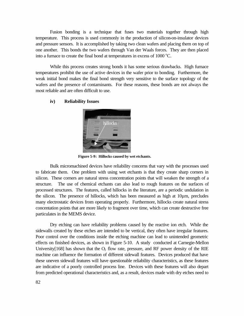
82
Fusion bonding is a technique that fuses two materials together through hightemperature. This process is used commonly in the production of silicon-on-insulator devicesand pressure sensors. It is accomplished by taking two clean wafers and placing them on top ofone another. This bonds the two wafers through Van der Waals forces. They are then placedinto a furnace to create the final bond at temperatures in excess of 1000 oC.
While this process creates strong bonds it has some serious drawbacks. High furnacetemperatures prohibit the use of active devices in the wafer prior to bonding. Furthermore, theweak initial bond makes the final bond strength very sensitive to the surface topology of thewafers and the presence of contaminants. For these reasons, these bonds are not always themost reliable and are often difficult to use.
iv) Reliability Issues
Bulk micromachined devices have reliability concerns that vary with the processes usedto fabricate them. One problem with using wet etchants is that they create sharp corners insilicon. These corners are natural stress concentration points that will weaken the strength of astructure. The use of chemical etchants can also lead to rough features on the surfaces ofprocessed structures. The features, called hillocks in the literature, are a periodic undulation inthe silicon. The presence of hillocks, which has been measured as high at 10µm, precludesmany electrostatic devices from operating properly. Furthermore, hillocks create natural stressconcentation points that are more likely to fragment over time, which can create destructive freeparticulates in the MEMS device.
Dry etching can have reliability problems caused by the reactive ion etch. While thesidewalls created by these etches are intended to be vertical, they often have irregular features.Poor control over the conditions inside the etching machine can lead to unintended geometriceffects on finished devices, as shown in Figure 5-10. A study conducted at Carnegie-MellonUniversity[168] has shown that the O2 flow rate, pressure, and RF power density of the RIEmachine can influence the formation of different sidewall features. Devices produced that havethese uneven sidewall features will have questionable reliability characteristics, as these featuresare indicative of a poorly controlled process line. Devices with these features will also departfrom predicted operational characteristics and, as a result, devices made with dry etches need to
Figure 5-9: Hillocks caused by wet etchants.
hillocks
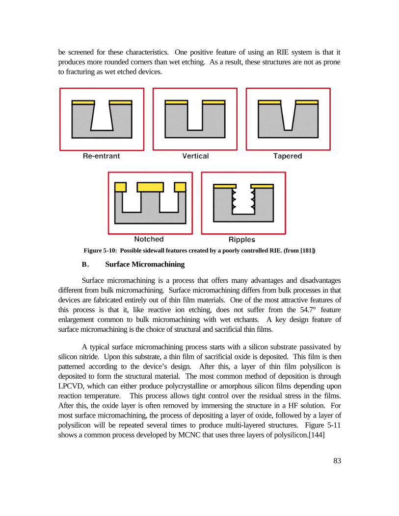
83
be screened for these characteristics. One positive feature of using an RIE system is that itproduces more rounded corners than wet etching. As a result, these structures are not as proneto fracturing as wet etched devices.
Figure 5-10: Possible sidewall features created by a poorly controlled RIE. (from [181])
B. Surface Micromachining
Surface micromachining is a process that offers many advantages and disadvantagesdifferent from bulk micromachining. Surface micromachining differs from bulk processes in thatdevices are fabricated entirely out of thin film materials. One of the most attractive features ofthis process is that it, like reactive ion etching, does not suffer from the 54.7° featureenlargement common to bulk micromachining with wet etchants. A key design feature ofsurface micromachining is the choice of structural and sacrificial thin films.
A typical surface micromachining process starts with a silicon substrate passivated bysilicon nitride. Upon this substrate, a thin film of sacrificial oxide is deposited. This film is thenpatterned according to the device’s design. After this, a layer of thin film polysilicon isdeposited to form the structural material. The most common method of deposition is throughLPCVD, which can either produce polycrystalline or amorphous silicon films depending uponreaction temperature. This process allows tight control over the residual stress in the films.After this, the oxide layer is often removed by immersing the structure in a HF solution. Formost surface micromachining, the process of depositing a layer of oxide, followed by a layer ofpolysilicon will be repeated several times to produce multi-layered structures. Figure 5-11shows a common process developed by MCNC that uses three layers of polysilicon.[144]

84
Figure 5-11: The surface micromachining process using three layers of polysilicon. (from [144])
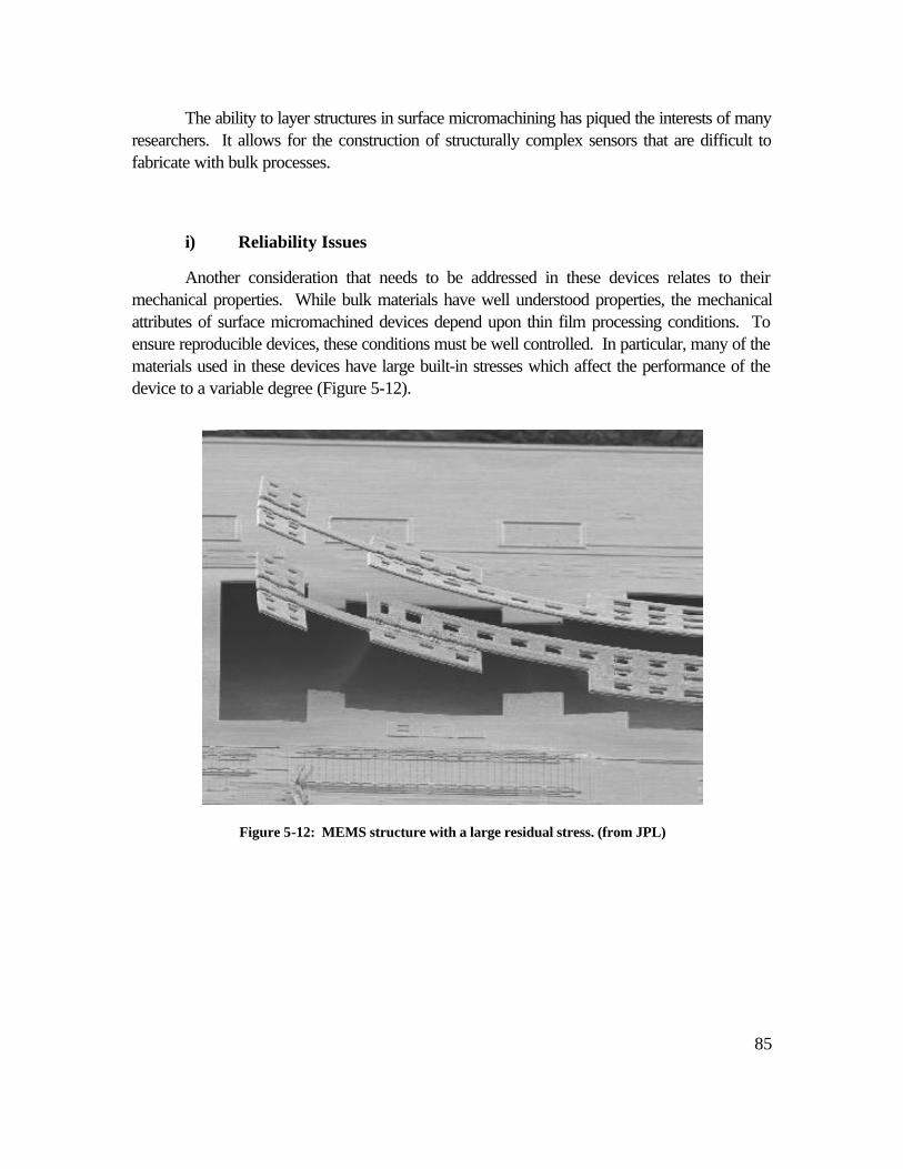
85
The ability to layer structures in surface micromachining has piqued the interests of manyresearchers. It allows for the construction of structurally complex sensors that are difficult tofabricate with bulk processes.
i) Reliability Issues
Another consideration that needs to be addressed in these devices relates to theirmechanical properties. While bulk materials have well understood properties, the mechanicalattributes of surface micromachined devices depend upon thin film processing conditions. Toensure reproducible devices, these conditions must be well controlled. In particular, many of thematerials used in these devices have large built-in stresses which affect the performance of thedevice to a variable degree (Figure 5-12).
Figure 5-12: MEMS structure with a large residual stress. (from JPL)
86
Surface micromachined devices also have adhesion problems that are inherently worsethan bulk micromachining. Cantilever beams are produced in surface micromachining on top ofa sacrificial oxide layer, which is removed by immersion in an HF bath. Then the structure iscleaned in de-ionized water. After this, a of 5-30Å thick oxide layer will form on the surface ofthe polysilicon. There will also be hydroxyl groups in the oxide layer, which have a high surfaceenergy. This makes the oxide layer extremely hydrophilic, which creates a strong capillary forcebetween the beams and the substrate. This capillary force will pull the beam to the substrateand create an adhesive bond between the beam and the substrate.
There are several methods now used to prevent released structures from bonding to thesubstrate. Several groups, including those led by R. Howe at Berkeley and N. Tien at Cornell,utilize a thin film of self assembled monolayers on the surface micromachined device. Themonolayers are hydrophobic, which creates a repulsive force between the substrate and thesuspended structures, which effectively prohibits adhesive bonds from forming. However, itremains unclear what impact the monolayers will have on the long term reliability of thesedevices. Another method that prevents the creation of adhesive bonds involves using polyimideas a sacrificial material. This technique, developed by Gregory Kovacs at Stanford University,utilizes aluminum structures that are released in an oxygen gas. Since this process does notutilize any liquids, no adhesive bonds are formed.
C. LIGA
LIGA is a German acronym that stands for lithography, electroplating, and molding.LIGA was developed to produce high aspect ratio structures. LIGA offers some uniqueproperties that makes it an interesting technology. LIGA enables the construction of structureswith the thickness of bulk micromachining with a degree of design freedom similar to surfacemicromachined devices. This technology offers structures several hundred microns thick, with aminimum feature size of only a few microns.
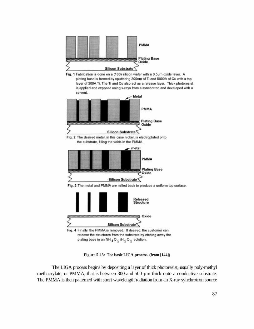
87
The LIGA process begins by depositing a layer of thick photoresist, usually poly-methylmethacrylate, or PMMA, that is between 300 and 500 µm thick onto a conductive substrate.The PMMA is then patterned with short wavelength radiation from an X-ray synchrotron source
Figure 5-13: The basic LIGA process. (from [144])
88
for several hours. Then a layer of metal is electroplated onto the exposed area of theconductive base plate, which fills in the open areas created by the patterning. Then the metalstructure is separated from the PMMA mold, as shown in Figure 5-13. This metal structure canin turn be used as a mold insert for injection molding to form multiple plastic replicas of theoriginal plating base. These plastic replicas can then be used to make multiple copies of theoriginal structure.
The LIGA technique involves some advances beyond semiconductor processing. TheX-ray source must be capable of delivering at least 1 GeV of energy at wavelengths shorter than7 Å. To withstand this bombardment, the opaque part of the mask must be constructed out of amaterial with a high atomic number. Furthermore, the transparent part of the mask must have alow atomic number to allow the photons to pass through without heavy absorption andscattering. Successful masks have been made with 3 µm thick gold in the opaque region and 1to 2 µm thick silicon nitride or titanium foil in the transparent region. Another hurdle toovercome is the electroplating of the patterned structure. This step requires accurate controllingof current density, temperature, concentration, and composition of the plating solution to preventthe formation of hydrogen bubbles, which can ruin a structure. These conditions also determinethe internal stress of the device and thus must be well understood and controlled to ensurereliable device operation.
i) Reliability Issues
LIGA, as a relatively costly technology, has not been researched as fully as otherMEMS processes. As a result, the LIGA process can have great variability across processruns. Another problem with LIGA is that the injection molding process and mold separationprocesses require almost perfectly vertical structures. This issue has become a strong factor inthe device yield of LIGA technology.
D. GaAs Processing
The processing of gallium arsenide can be as varied as silicon processing. While thereare many GaAs processes that are very similar to those of silicon, there are some techniquesthat are unique to GaAs. These GaAs processing techniques are an offshoot of bulkmicromachining that utilizes the unique properties of GaAs and its ternary alloy AlGaAs toproduce structures.
One method of processing GaAs wafers is to use ion implantation. The first step is tolayer an implantation mask. Then a layer of N ions is implanted into the substrate. The depththat they travel into the substrate is a function of accelerating voltage. Then the mask is removedand the sample is annealed at 750oC for about 30 minutes while covered with PECVD Si3N4.This process recrystalizes the buried layer to a GaAs1-xNx layer. Then a SiO2 etch mask isevaporated onto the surface of the wafer. Then an anisotropic etch is performed to expose the
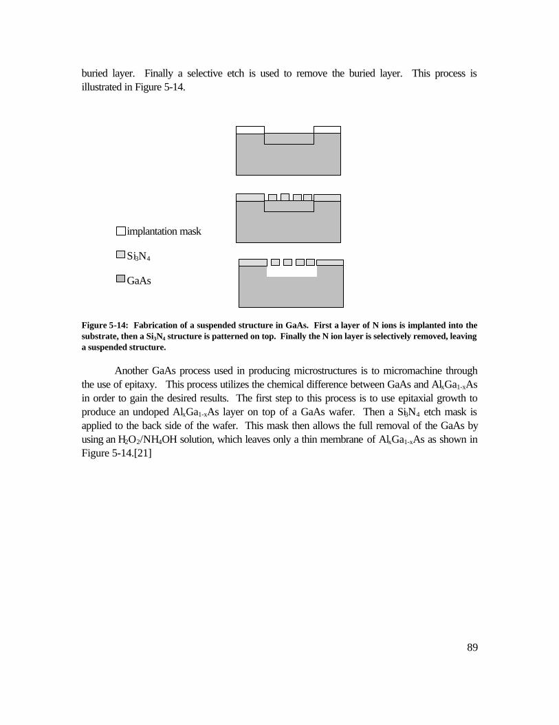
89
buried layer. Finally a selective etch is used to remove the buried layer. This process isillustrated in Figure 5-14.
Figure 5-14: Fabrication of a suspended structure in GaAs. First a layer of N ions is implanted into thesubstrate, then a Si3N4 structure is patterned on top. Finally the N ion layer is selectively removed, leavinga suspended structure.
Another GaAs process used in producing microstructures is to micromachine throughthe use of epitaxy. This process utilizes the chemical difference between GaAs and AlxGa1-xAsin order to gain the desired results. The first step to this process is to use epitaxial growth toproduce an undoped AlxGa1-xAs layer on top of a GaAs wafer. Then a Si3N4 etch mask isapplied to the back side of the wafer. This mask then allows the full removal of the GaAs byusing an H2O2/NH4OH solution, which leaves only a thin membrane of AlxGa1-xAs as shown inFigure 5-14.[21]
implantation mask
Si3N4
GaAs
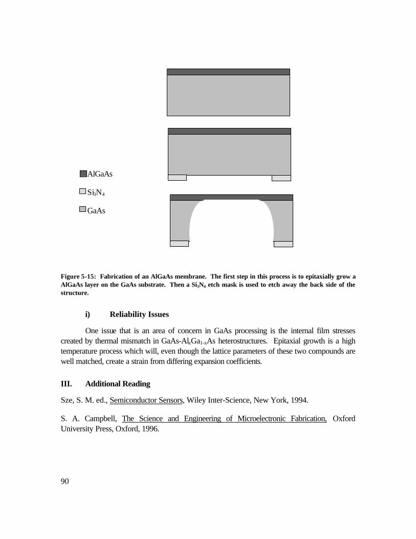
90
Figure 5-15: Fabrication of an AlGaAs membrane. The first step in this process is to epitaxially grow aAlGaAs layer on the GaAs substrate. Then a Si3N4 etch mask is used to etch away the back side of thestructure.
i) Reliability Issues
One issue that is an area of concern in GaAs processing is the internal film stressescreated by thermal mismatch in GaAs-AlxGa1-xAs heterostructures. Epitaxial growth is a hightemperature process which will, even though the lattice parameters of these two compounds arewell matched, create a strain from differing expansion coefficients.
III. Additional Reading
Sze, S. M. ed., Semiconductor Sensors, Wiley Inter-Science, New York, 1994.
S. A. Campbell, The Science and Engineering of Microelectronic Fabrication, OxfordUniversity Press, Oxford, 1996.
AlGaAs
Si3N4
GaAs

91
Chapter 6: Common Device Elements
B. Stark
While a completed MEMS is a complicated device, the individual components of anygiven system are much simpler to understand. Due to the nature of MEMS processing, nosingle component can be very complex. This in turn means that understanding of a MEMSdevice can be gained through knowledge of a few simple parts and understanding how theyinteract. To ensure the reliable operation of a MEMS device it is sufficient to ensure the reliableoperation of all the constituent parts.
One of the difficulties in writing a guideline is trying to select material that will not bedated before the book goes to press. To preclude this problem, this chapter does not addressspecific sensor technologies, but rather it deals with device elements. It is assumed that aknowledgeable reliability engineer can construe all the necessary information on, for example, acapacitive accelerometer by examining the sections on structural beams and parallel platecapacitors. It is felt that this arrangement of the material will increase its useful lifetime.
This chapter has been loosely organized into three sections. The first three subchaptersdiscuss structural elements in MEMS. The next two subchapters, along with part of the third,discuss transducer elements. The remainder of the chapter is dedicated to actuatortechnologies.
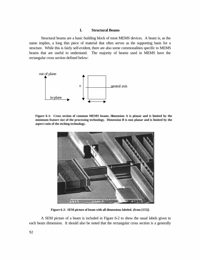
92
I. Structural Beams
Structural beams are a basic building block of most MEMS devices. A beam is, as thename implies, a long thin piece of material that often serves as the supporting basis for astructure. While this is fairly self-evident, there are also some commonalities specific to MEMSbeams that are useful to understand. The majority of beams used in MEMS have therectangular cross section defined below:
Figure 6-2: SEM picture of beam with all dimensions labeled. (from [155])
A SEM picture of a beam is included in Figure 6-2 to show the usual labels given toeach beam dimension. It should also be noted that the rectangular cross section is a generally
Figure 6-1: Cross section of common MEMS beams. Dimension A is planar and is limited by theminimum feature size of the processing technology. Dimension B is non planar and is limited by theaspect ratio of the etching technology.
B neutral axis
out of plane
in-plane
B
A
l
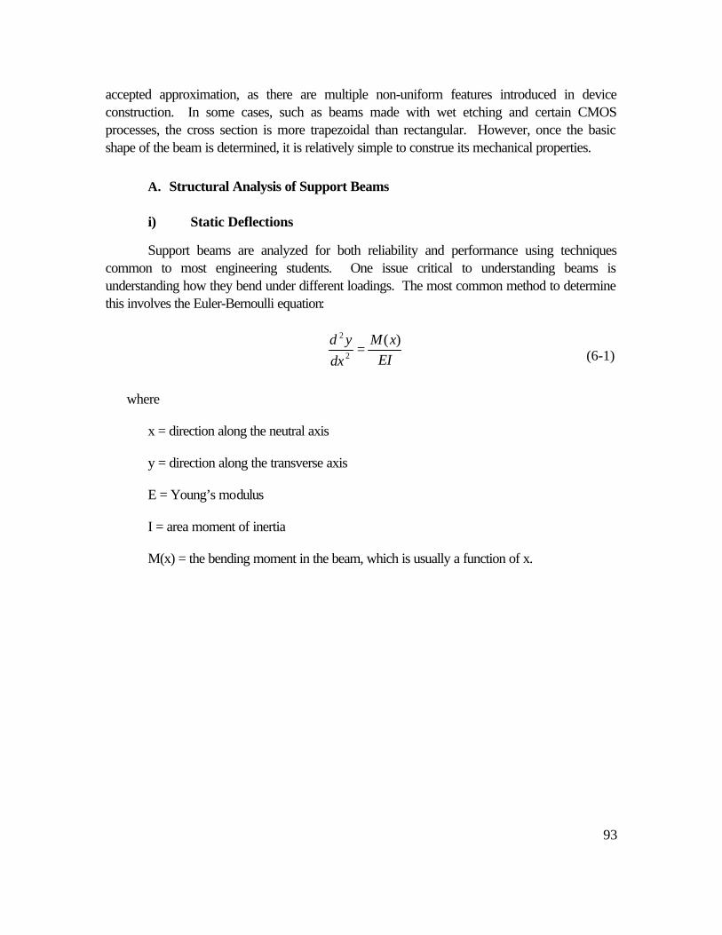
93
accepted approximation, as there are multiple non-uniform features introduced in deviceconstruction. In some cases, such as beams made with wet etching and certain CMOSprocesses, the cross section is more trapezoidal than rectangular. However, once the basicshape of the beam is determined, it is relatively simple to construe its mechanical properties.
A. Structural Analysis of Support Beams
i) Static Deflections
Support beams are analyzed for both reliability and performance using techniquescommon to most engineering students. One issue critical to understanding beams isunderstanding how they bend under different loadings. The most common method to determinethis involves the Euler-Bernoulli equation:
where
x = direction along the neutral axis
y = direction along the transverse axis
E = Young’s modulus
I = area moment of inertia
M(x) = the bending moment in the beam, which is usually a function of x.
EIxM
dxyd )(2
2
= (6-1)
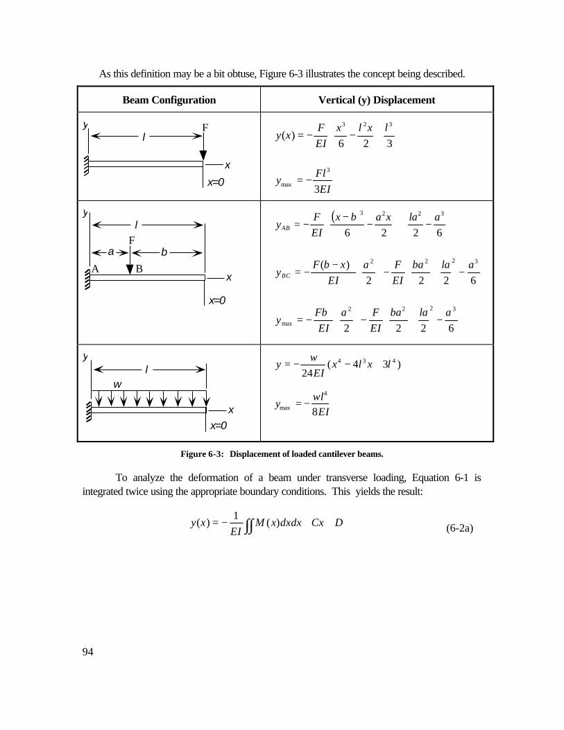
94
As this definition may be a bit obtuse, Figure 6-3 illustrates the concept being described.
Beam Configuration Vertical (y) Displacement
ly
x
F
+−−=
326)(
323 lxlxEIF
xy
EIFl
y3
3
max −=
ly
x
a bA B
F
( )
−+−
−−=
6226
3223 alaxabxEIF
yAB
−+−
−−=
6222)( 3222 alaba
EIFa
EIxbF
yBC
−+−
−=
6222
3222
maxalaba
EIFa
EIFb
y
ly
x
w
)34(24
434 lxlxEI
wy +−−=
ymax = −wl4
8EI
Figure 6-3: Displacement of loaded cantilever beams.
To analyze the deformation of a beam under transverse loading, Equation 6-1 isintegrated twice using the appropriate boundary conditions. This yields the result:
∫∫ ++−= DCxdxdxxMEI
xy )(1
)( (6-2a)
x=0
x=0
x=0
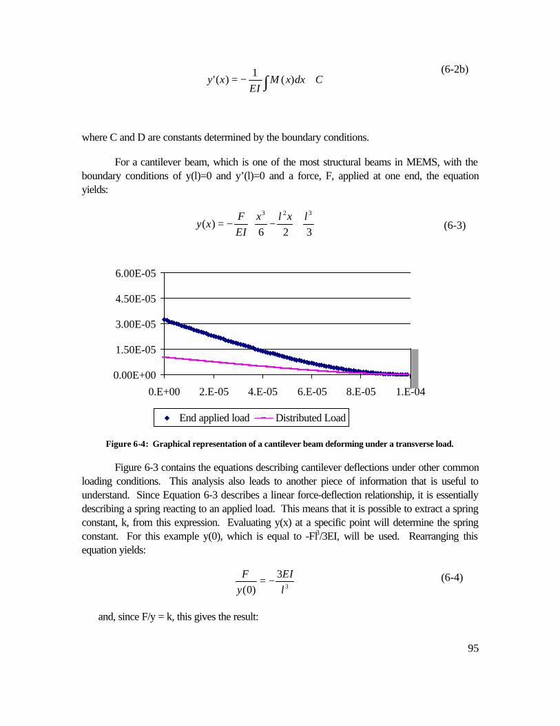
95
∫ +−= CdxxMEI
xy )(1
)('
where C and D are constants determined by the boundary conditions.
For a cantilever beam, which is one of the most structural beams in MEMS, with theboundary conditions of y(l)=0 and y’(l)=0 and a force, F, applied at one end, the equationyields:
+−−=
326)(
323 lxlxEIF
xy
Figure 6-4: Graphical representation of a cantilever beam deforming under a transverse load.
Figure 6-3 contains the equations describing cantilever deflections under other commonloading conditions. This analysis also leads to another piece of information that is useful tounderstand. Since Equation 6-3 describes a linear force-deflection relationship, it is essentiallydescribing a spring reacting to an applied load. This means that it is possible to extract a springconstant, k, from this expression. Evaluating y(x) at a specific point will determine the springconstant. For this example y(0), which is equal to -Fl3/3EI, will be used. Rearranging thisequation yields:
3
3)0( l
EIyF
−=
and, since F/y = k, this gives the result:
(6-2b)
(6-3)
(6-4)
0.00E+00
1.50E-05
3.00E-05
4.50E-05
6.00E-05
0.E+00 2.E-05 4.E-05 6.E-05 8.E-05 1.E-04
End applied load Distributed Load
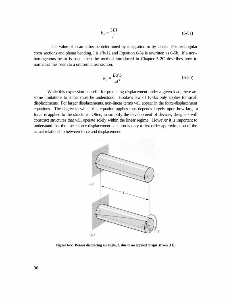
96
3
3lEI
k y =
The value of I can either be determined by integration or by tables. For rectangularcross sections and planar bending, I is a3b/12 and Equation 6-5a is rewritten as 6-5b. If a non-homogenous beam is used, then the method introduced in Chapter 5-2C describes how tonormalize this beam to a uniform cross section.
3
3
4lbEa
k y =
While this expression is useful for predicting displacement under a given load, there aresome limitations to it that must be understood. Hooke’s law of Fx=kx only applies for smalldisplacements. For larger displacements, non-linear terms will appear in the force-displacementequations. The degree to which this equation applies thus depends largely upon how large aforce is applied to the structure. Often, to simplify the development of devices, designers willconstruct structures that will operate solely within the linear regime. However it is important tounderstand that the linear force-displacement equation is only a first order approximation of theactual relationship between force and displacement.
Figure 6-5: Beams displacing an angle, φ, due to an applied torque. (from [11])
(6-5a)
(6-5b)
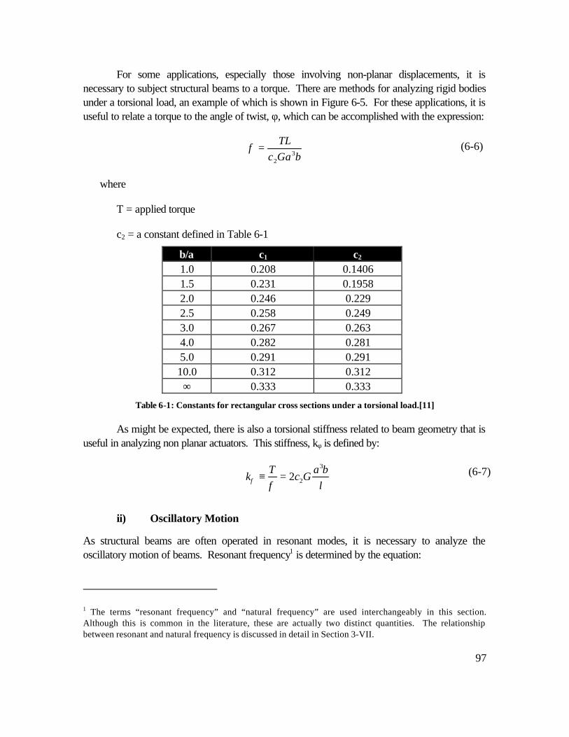
97
For some applications, especially those involving non-planar displacements, it isnecessary to subject structural beams to a torque. There are methods for analyzing rigid bodiesunder a torsional load, an example of which is shown in Figure 6-5. For these applications, it isuseful to relate a torque to the angle of twist, φ, which can be accomplished with the expression:
bGacTL
32
=φ
where
T = applied torque
c2 = a constant defined in Table 6-1
b/a c1 c2
1.0 0.208 0.14061.5 0.231 0.19582.0 0.246 0.2292.5 0.258 0.2493.0 0.267 0.2634.0 0.282 0.2815.0 0.291 0.29110.0 0.312 0.312∞ 0.333 0.333
Table 6-1: Constants for rectangular cross sections under a torsional load.[11]
As might be expected, there is also a torsional stiffness related to beam geometry that isuseful in analyzing non planar actuators. This stiffness, kφ is defined by:
lba
GcT
k3
22=≡φφ
ii) Oscillatory Motion
As structural beams are often operated in resonant modes, it is necessary to analyze theoscillatory motion of beams. Resonant frequency1 is determined by the equation:
1 The terms “resonant frequency” and “natural frequency” are used interchangeably in this section.Although this is common in the literature, these are actually two distinct quantities. The relationshipbetween resonant and natural frequency is discussed in detail in Section 3-VII.
(6-6)
(6-7)
98
effmk
=0ω
where
k = stiffness or spring constant
meff = moving mass
The only two quantities required to determine the natural frequency of a beam are k and meff.Since k has already been derived, it is necessary to calculate the moving mass. The movingmass can be analytically determined using Rayleigh’s method. However, this method exceedsthe scope of the guideline. It suffices to know that, for a cantilever beam, the moving mass isroughly 23% of the total mass. This can be analytically described by
ablmeff ρ23.=
where ρ is the mass density of the beam. This leads to a final expression for resonantfrequency:
ρω
Ela20 043.1=
In cases when beams oscillate in torsion, the torsional resonant frequency is:
φ
φωI
k=0
Since beams driven by harmonic transverse loads behave similarly to strings in tension,the wave equation can describe analytically how a beam moves in resonance:
2
2
ty
lm
xF
∂∂
−=∂∂
Through a substitution of the force for an expression involving the moment, thisequation becomes:
2
2
2
2
2
2
ty
lm
xy
EIx ∂
∂=
∂∂
∂∂
−
(6-8)
(6-9)
(6-10)
(6-11)
(6-12a)
(6-12b)
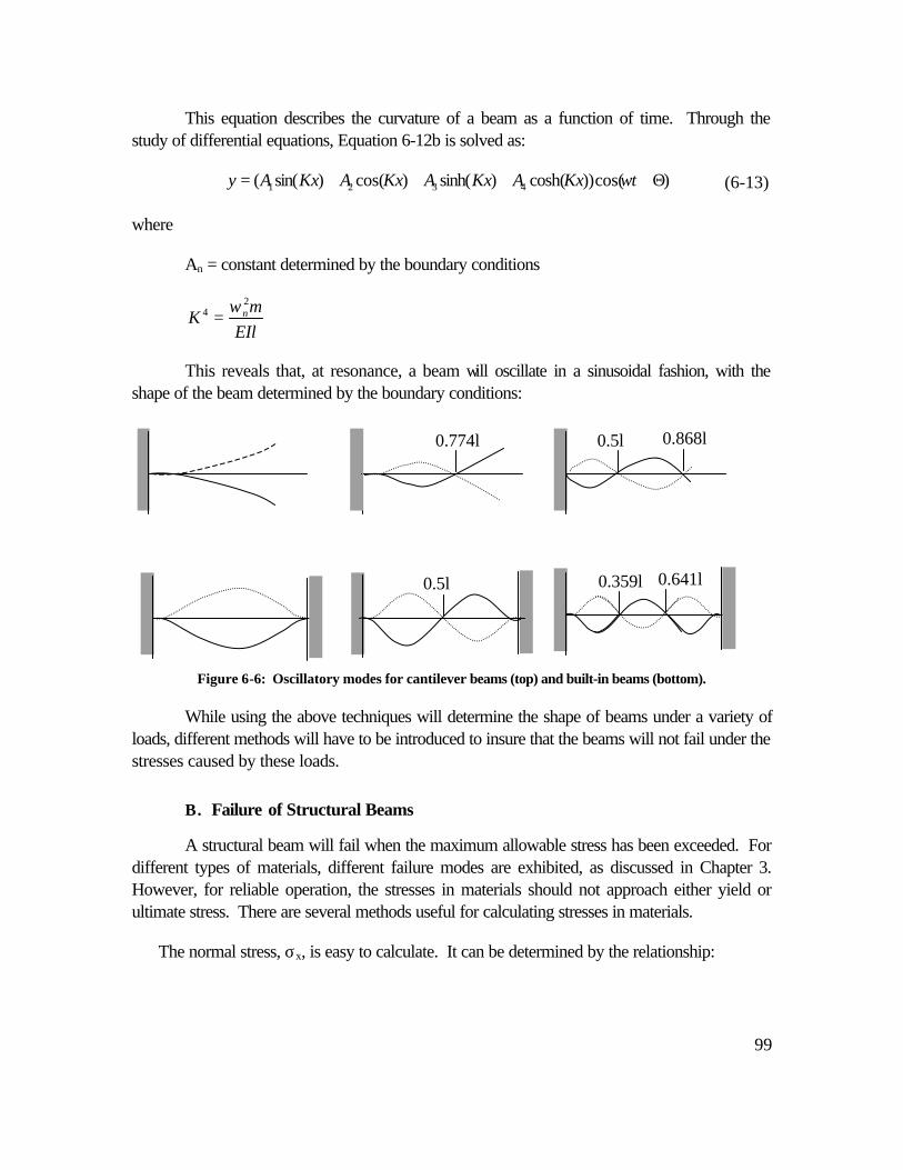
99
This equation describes the curvature of a beam as a function of time. Through thestudy of differential equations, Equation 6-12b is solved as:
)cos())cosh()sinh()cos()sin(( 4321 Θ++++= tKxAKxAKxAKxAy ω
where
An = constant determined by the boundary conditions
EIlm
K n2
4 ω=
This reveals that, at resonance, a beam will oscillate in a sinusoidal fashion, with theshape of the beam determined by the boundary conditions:
Figure 6-6: Oscillatory modes for cantilever beams (top) and built-in beams (bottom).
While using the above techniques will determine the shape of beams under a variety ofloads, different methods will have to be introduced to insure that the beams will not fail under thestresses caused by these loads.
B. Failure of Structural Beams
A structural beam will fail when the maximum allowable stress has been exceeded. Fordifferent types of materials, different failure modes are exhibited, as discussed in Chapter 3.However, for reliable operation, the stresses in materials should not approach either yield orultimate stress. There are several methods useful for calculating stresses in materials.
The normal stress, σx, is easy to calculate. It can be determined by the relationship:
(6-13)
0.774l 0.5l 0.868l
0.5l 0.359l 0.641l
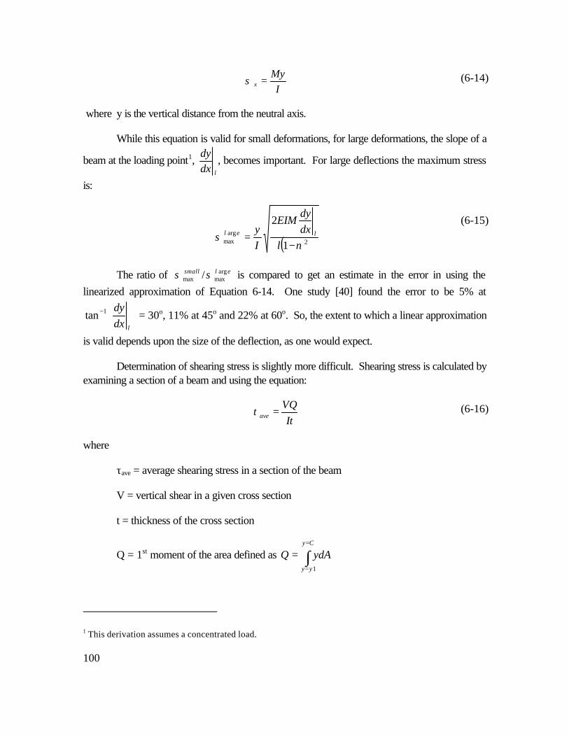
100
IMy
x =σ
where y is the vertical distance from the neutral axis.
While this equation is valid for small deformations, for large deformations, the slope of a
beam at the loading point1, ldx
dy, becomes important. For large deflections the maximum stress
is:
( )2arg
max 1
2
νσ
−=
ldxdy
EIM
Iy lel
The ratio of elsmall argmaxmax /σσ is compared to get an estimate in the error in using the
linearized approximation of Equation 6-14. One study [40] found the error to be 5% at
−
ldxdy1tan = 30o, 11% at 45o and 22% at 60o. So, the extent to which a linear approximation
is valid depends upon the size of the deflection, as one would expect.
Determination of shearing stress is slightly more difficult. Shearing stress is calculated byexamining a section of a beam and using the equation:
ItVQ
ave =τ
where
τave = average shearing stress in a section of the beam
V = vertical shear in a given cross section
t = thickness of the cross section
Q = 1st moment of the area defined as ∫=
=
=Cy
yy
ydAQ1
1 This derivation assumes a concentrated load.
(6-14)
(6-15)
(6-16)
101
The relationship among all of these values is presented in Figure 6-7. To determine τmax,
it is usually necessary to examine τave as a function of y. For beams with the height > 4×width,the approximation of τmax=1.5×V/(w×h) is useful. However, for planar bending in beams,where the b ≥ a relationship obviates this approximation, the full structural analysis will have tobe performed. It is convenient to recognize that maximum shearing stress will always occuralong the neutral axis, unless there are marked variations in beam thickness. Thus, determinationof shearing stress in beams can usually be performed simply by examining τave at y=0.
For rectangular beams subjected to a torque, there will be a shear stress that will varyas a function of horizontal and vertical position. However the study of mechanics reveals thatthe maximum stress, which is the most important in terms of structural analysis, occurs along theneutral axis of the wider face of the beam, which, in this discussion, is labeled as b. Thismaximum shearing stress is determined by the relation:
bacT
21
max =τ
where c1 is a constant defined in Table 6-1.
While using the above analysis leads to a good understanding of when fracture willoccur, there are other failure modes in structural beams. Beams will usually fail if they come intocontact with other structures, due to adhesive forces. To analyze the probability of this, thedeflection of every beam must be considered under maximum load.
(6-17)
y
A
Figure 6-7: Side (top) and cross sectional (bottom) views of cantilever beamunder shear force and bending movement.
C
y1
t
y = 0 (neutral axis)
l
MV
x
102
Another concern raised in Chapter 3 was the impact of fatigue in beams. Over longcycle times, the properties of beams will shift, which, as this section has shown, will change thestatic and resonant characteristics of the structures. These changes will alter the output of manysensors based upon measuring frequency and deflection. Another fatigue related mechanism isthe gradual relaxation of the fracture strength of a material. Beams that were initially drivenwithin stress tolerances of a material, can be driven past them, as the tolerances decrease.Although it should be noted again that this mechanism has yet to be observed in silicon.
Thermal changes can also have an impact upon beam reliability. Thermal stressing andunstressing creates mechanical fatigue in beams. In large temperature changes, as experiencedin the space environment, most MEMS beams will also experience bimetallic warping due to thefact that they are made of different materials that have mismatched thermal coefficients ofexpansions. Thermal fatigue can also contribute to delamination.
C. Additional Reading
F. P. Beer and E. R. Johnston, Mechanics of Materials: Second Edition, McGraw-Hill.New York, 1992.
C. M. Harris and C. E. Crede, Shock and Vibration Handbook Volume 1: Basic Theory andMeasurements, McGraw-Hill Book Company, Inc., New York, 1961.
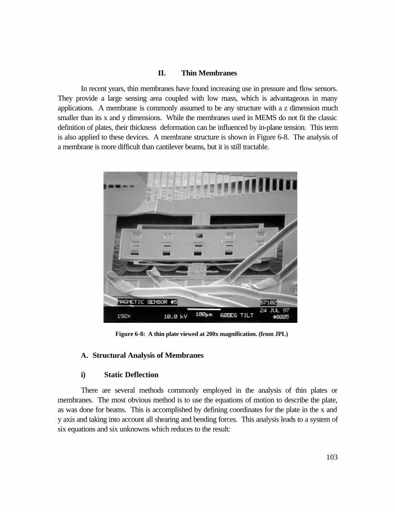
103
II. Thin Membranes
In recent years, thin membranes have found increasing use in pressure and flow sensors.They provide a large sensing area coupled with low mass, which is advantageous in manyapplications. A membrane is commonly assumed to be any structure with a z dimension muchsmaller than its x and y dimensions. While the membranes used in MEMS do not fit the classicdefinition of plates, their thickness deformation can be influenced by in-plane tension. This termis also applied to these devices. A membrane structure is shown in Figure 6-8. The analysis ofa membrane is more difficult than cantilever beams, but it is still tractable.
A. Structural Analysis of Membranes
i) Static Deflection
There are several methods commonly employed in the analysis of thin plates ormembranes. The most obvious method is to use the equations of motion to describe the plate,as was done for beams. This is accomplished by defining coordinates for the plate in the x andy axis and taking into account all shearing and bending forces. This analysis leads to a system ofsix equations and six unknowns which reduces to the result:
Figure 6-8: A thin plate viewed at 200x magnification. (from JPL)
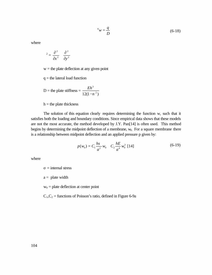
104
Dq
w =∇ 4
where
∇2 = 2
2
2
2
yx ∂∂
+∂∂
w = the plate deflection at any given point
q = the lateral load function
D = the plate stiffness = )1(12 2
3
ν−Eh
h = the plate thickness
The solution of this equation clearly requires determining the function w, such that itsatisfies both the loading and boundary conditions. Since empirical data shows that these modelsare not the most accurate, the method developed by J.Y. Pan[14] is often used. This methodbegins by determining the midpoint deflection of a membrane, w0. For a square membrane thereis a relationship between midpoint deflection and an applied pressure p given by:
30420210)( w
ahE
Cwah
Cwp +=σ
[14]
where
σ = internal stress
a = plate width
w0 = plate deflection at center point
C1,C2 = functions of Poisson’s ratio, defined in Figure 6-9a
(6-18)
(6-19)
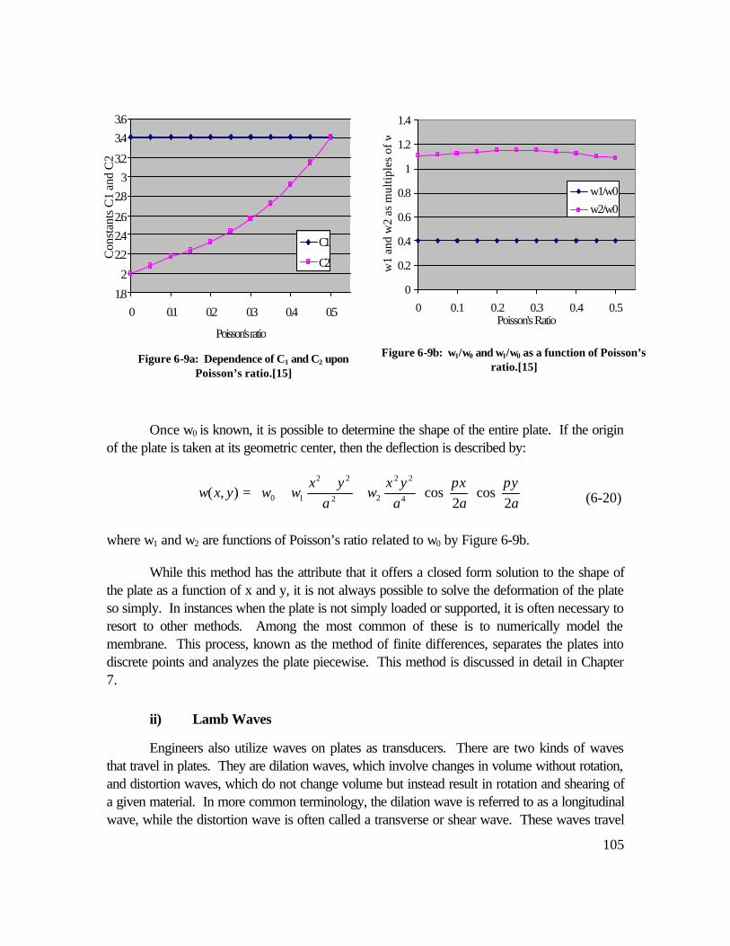
105
Once w0 is known, it is possible to determine the shape of the entire plate. If the originof the plate is taken at its geometric center, then the deflection is described by:
+
++=
ay
ax
ayx
wa
yxwwyxw
2cos
2cos),( 4
22
22
22
10
ππ
where w1 and w2 are functions of Poisson’s ratio related to w0 by Figure 6-9b.
While this method has the attribute that it offers a closed form solution to the shape ofthe plate as a function of x and y, it is not always possible to solve the deformation of the plateso simply. In instances when the plate is not simply loaded or supported, it is often necessary toresort to other methods. Among the most common of these is to numerically model themembrane. This process, known as the method of finite differences, separates the plates intodiscrete points and analyzes the plate piecewise. This method is discussed in detail in Chapter7.
ii) Lamb Waves
Engineers also utilize waves on plates as transducers. There are two kinds of wavesthat travel in plates. They are dilation waves, which involve changes in volume without rotation,and distortion waves, which do not change volume but instead result in rotation and shearing ofa given material. In more common terminology, the dilation wave is referred to as a longitudinalwave, while the distortion wave is often called a transverse or shear wave. These waves travel
(6-20)
1.8
2
2.22.42.6
2.83
3.2
3.43.6
0 0.1 0.2 0.3 0.4 0.5
Poisson's ratio
Con
stan
ts C
1 an
d C
2
C1
C2
Figure 6-9a: Dependence of C1 and C2 uponPoisson’s ratio.[15]
0
0.2
0.4
0.6
0.8
1
1.2
1.4
0 0.1 0.2 0.3 0.4 0.5Poisson's Ratio
w1
and
w2
as m
ultip
les
of w
0
w1/w0w2/w0
Figure 6-9b: w1/w0 and w1/w0 as a function of Poisson’sratio.[15]
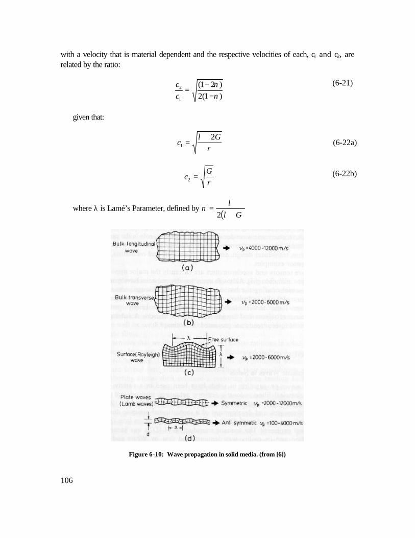
106
with a velocity that is material dependent and the respective velocities of each, c1 and c2, arerelated by the ratio:
)1(2)21(
1
2
νν
−−
=cc
given that:
ρλ G
c2
1
+=
ρG
c =2
where λ is Lamé’s Parameter, defined by ( )G+
=λ
λν
2
Figure 6-10: Wave propagation in solid media. (from [6])
(6-21)
(6-22a)
(6-22b)
107
In plates, these two waves interact in complex ways at the plate boundaries, whichresults in the formation of a plate wave, which is also called a lamb wave. These waves travel ineither symmetric or anti symmetric modes as shown in Figure 6-10. The lowest order of thesemodes are very similar to surface acoustical waves, or SAW, that propagate along a semi-infinite medium. However, in thin plates, the lowest order symmetric mode is dispersionless andpropagates much faster than a SAW on the same materials. The lowest order anti-symmetricmode, on the other hand, involves flexure and its wave velocity decreases monotonically to zeroas the plate becomes infinitely thin.[51] Lamb waves travel with a phase and group velocity thatis defined by:
ρ3
12h
Dvps = psgs vv =
=
ρ3hD
whvpa paga vv 2=
where g and p represent group and phase, and s and a represent symmetric and anti-symmetric.
One of the interesting results of this analysis is that tension and wave velocity arecoupled. If a small section of a plate is considered with dimensions, dx and dy, and a tension, T,in the x-direction, the out of plane force on the plate can be modeled by two forces, a stiffnessand a tension:
dxdyxw
DdFzS 4
4
∂∂
−=
dxdyxw
TdFzT 2
2
∂∂
=
If these equations are combined and related to the acceleration of the membrane, theresult is:
2
2
2
2
4
4
tw
Mdxdydxdyxw
Tdxdyxw
D∂∂
=∂∂
+∂∂
−
where M is the mass per unit area of the membrane
If this equation is solved through separation of variables, one finds that the solution is:
)(),( xktjn
nneCtxw −= ω
where
(6-23a)
(6-23b)
(6-24a)
(6-24b)
(6-24c)
(6-25)
108
+= D
Pn
tMP
nn
2212 ππω
P = period of the actuator that is oscillating the plate
n = integer representing the different modes of the device
This leads to the solution that the phase velocity is dependent on tension and mass:
M
DP
nT
vp
π2+
≈
As this analysis shows, the phase velocity is coupled to both the tension and massdensity of the plate. This enables sensors that detect lamb waves to be sensitive to a wide rangeof different effects, with temperature and pressure changes being the more prevalent changessensed. The advantage of using anti-symmetric lamb waves in sensors is that, on very thinplates, they have a phase velocity that is usually much slower than that of sound in most media.This allows these devices to transmit waves without dissipating large amounts of energy to thesurrounding environment. In comparison to surface acoustic waves, which dissipate on theorder of 1 dB per wavelength, lamb waves have extremely low loss mechanisms. In lambwaves, the disturbance to the surrounding medium only extends to a distance of λ/2π , whichlimits the acoustical energy loss. For an in-depth discussion of the physical properties of Lambwaves, Reference [115] treats the material more thoroughly.
iii) Modal Waves
While lamb waves have many applications in membranes, it is also useful to excitestanding waves on plates. A standing wave, as opposed to a lamb wave, involves oscillations infixed spots. These waves have maximum displacement at the resonant frequency of a device.On a resonating plate, there will be distinct spots called nodes, where vertical motion isessentially zero, and spots called anti-nodes, where oscillations are maximized. The analysis ofstanding waves begins with a dynamic version of Equation 6-18:
2
22
2
224
yW
Nyx
WN
xW
NWMhWD yxyxn ∂∂
+∂∂
∂+
∂∂
+=∇ ω
where
(6-26)
(6-27)
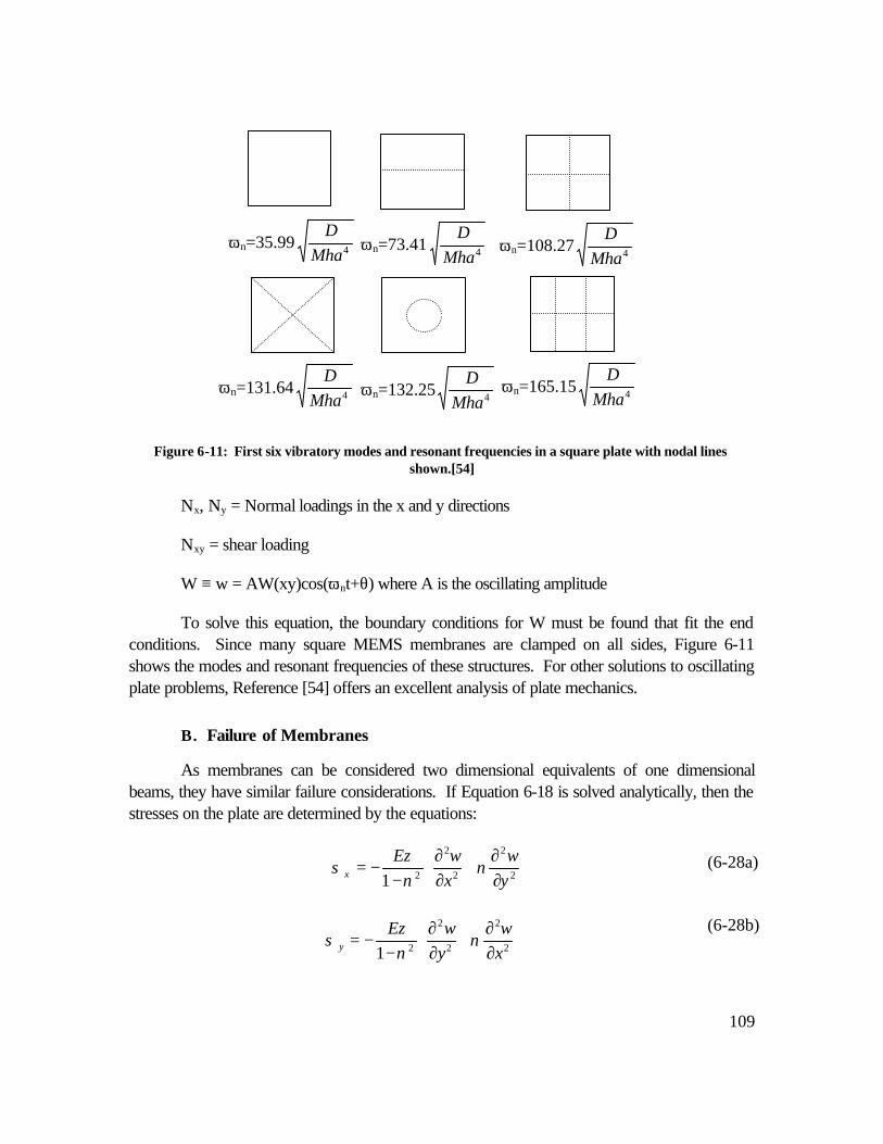
109
Figure 6-11: First six vibratory modes and resonant frequencies in a square plate with nodal linesshown.[54]
Nx, Ny = Normal loadings in the x and y directions
Nxy = shear loading
W ≡ w = AW(xy)cos(ωnt+θ) where A is the oscillating amplitude
To solve this equation, the boundary conditions for W must be found that fit the endconditions. Since many square MEMS membranes are clamped on all sides, Figure 6-11shows the modes and resonant frequencies of these structures. For other solutions to oscillatingplate problems, Reference [54] offers an excellent analysis of plate mechanics.
B. Failure of Membranes
As membranes can be considered two dimensional equivalents of one dimensionalbeams, they have similar failure considerations. If Equation 6-18 is solved analytically, then thestresses on the plate are determined by the equations:
∂∂
+∂∂
−−= 2
2
2
2
21 yw
xwEz
x νν
σ
∂∂
+∂∂
−−= 2
2
2
2
21 xw
ywEz
y νν
σ
(6-28a)
(6-28b)
ωn=35.99 4MhaD
ωn=73.41 4MhaD
ωn=108.27 4MhaD
ωn=131.64 4MhaD
ωn=132.25 4MhaD ωn=165.15 4Mha
D
110
yxwEz
xy ∂∂∂
+=
2
1 ντ
where z is the distance from the neutral axis of the plate
In order to determine the maximum stress in a plate, the following relationships are alsouseful:
∂∂
+∂∂
−= 2
2
2
2
yw
vxw
DM x
∂∂
+∂∂
−= 2
2
2
2
xw
vyw
DM y
If the bending moments are known, the stress distribution can be calculated. Stress iszero along the neutral axis and rises linearly to a maximum at the surface. This maximum valueis:
2max6
)(hM x
x =σ
2max
6)(
h
M yy =σ
This analysis can be simplified for a membrane with a uniform loading, q, and fixedboundary conditions on all four sides. These structures will have the following stresses:
a
b
stress at center of long edge: 2
21
max tqbβ
σ−
= (6-31a)
stress at center: 2
22
tqbβ
σ = (6-31b)
The parameters α, β1 and β2 are functions of the plate geometry and boundary conditions, andmay be determined from the table below:
(6-28c)
(6-29a)
(6-29b)
(6-30a)
(6-30b)
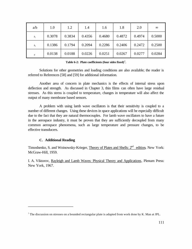
111
a/b 1.0 1.2 1.4 1.6 1.8 2.0 ∞
β1 0.3078 0.3834 0.4356 0.4680 0.4872 0.4974 0.5000
β2 0.1386 0.1794 0.2094 0.2286 0.2406 0.2472 0.2500
α 0.0138 0.0188 0.0226 0.0251 0.0267 0.0277 0.0284
Table 6-2: Plate coefficients (four sides fixed)1.
Solutions for other geometries and loading conditions are also available; the reader isreferred to References [58] and [59] for additional information.
Another area of concern in plate mechanics is the effects of internal stress upondeflection and strength. As discussed in Chapter 3, thin films can often have large residualstresses. As this stress is coupled to temperature, changes in temperature will also affect theoutput of many membrane based sensors.
A problem with using lamb wave oscillators is that their sensitivity is coupled to anumber of different changes. Using these devices in space applications will be especially difficultdue to the fact that they are natural thermocouples. For lamb wave oscillators to have a futurein the aerospace industry, it must be proven that they are sufficiently decoupled from manycommon aerospace phenomena, such as large temperature and pressure changes, to beeffective transducers.
C. Additional Reading
Timoshenko, S. and Woinowsky-Krieger, Theory of Plates and Shells: 2nd edition, New York:McGraw-Hill, 1959.
I. A. Viktorov, Rayleigh and Lamb Waves: Physical Theory and Applications, Plenum Press:New York, 1967.
1 The discussion on stresses on a bounded rectangular plate is adapted from work done by K. Man at JPL.
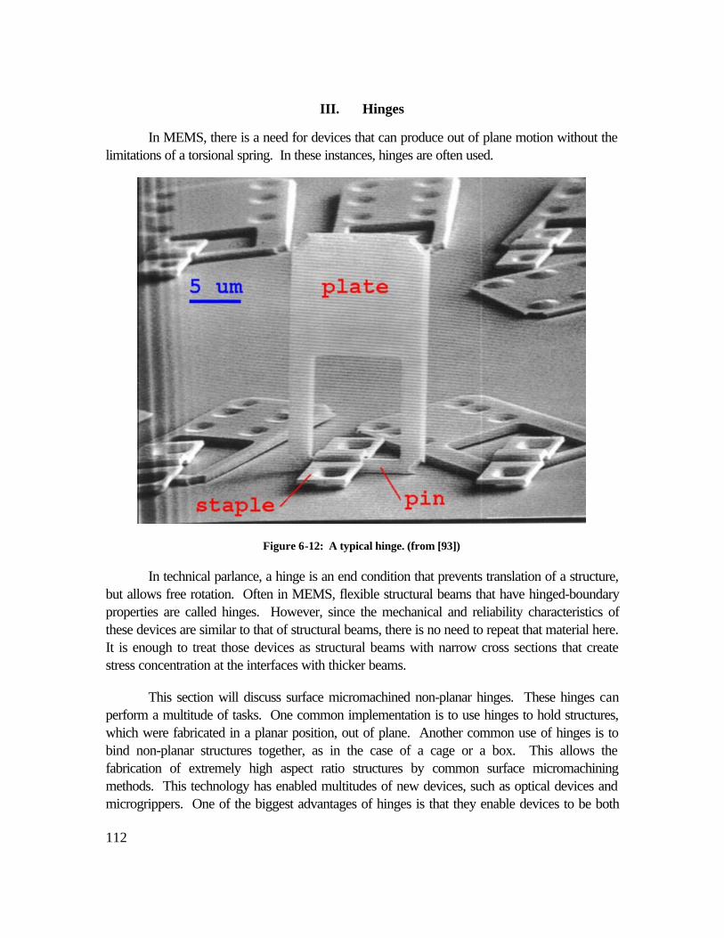
112
III. Hinges
In MEMS, there is a need for devices that can produce out of plane motion without thelimitations of a torsional spring. In these instances, hinges are often used.
Figure 6-12: A typical hinge. (from [93])
In technical parlance, a hinge is an end condition that prevents translation of a structure,but allows free rotation. Often in MEMS, flexible structural beams that have hinged-boundaryproperties are called hinges. However, since the mechanical and reliability characteristics ofthese devices are similar to that of structural beams, there is no need to repeat that material here.It is enough to treat those devices as structural beams with narrow cross sections that createstress concentration at the interfaces with thicker beams.
This section will discuss surface micromachined non-planar hinges. These hinges canperform a multitude of tasks. One common implementation is to use hinges to hold structures,which were fabricated in a planar position, out of plane. Another common use of hinges is tobind non-planar structures together, as in the case of a cage or a box. This allows thefabrication of extremely high aspect ratio structures by common surface micromachiningmethods. This technology has enabled multitudes of new devices, such as optical devices andmicrogrippers. One of the biggest advantages of hinges is that they enable devices to be both
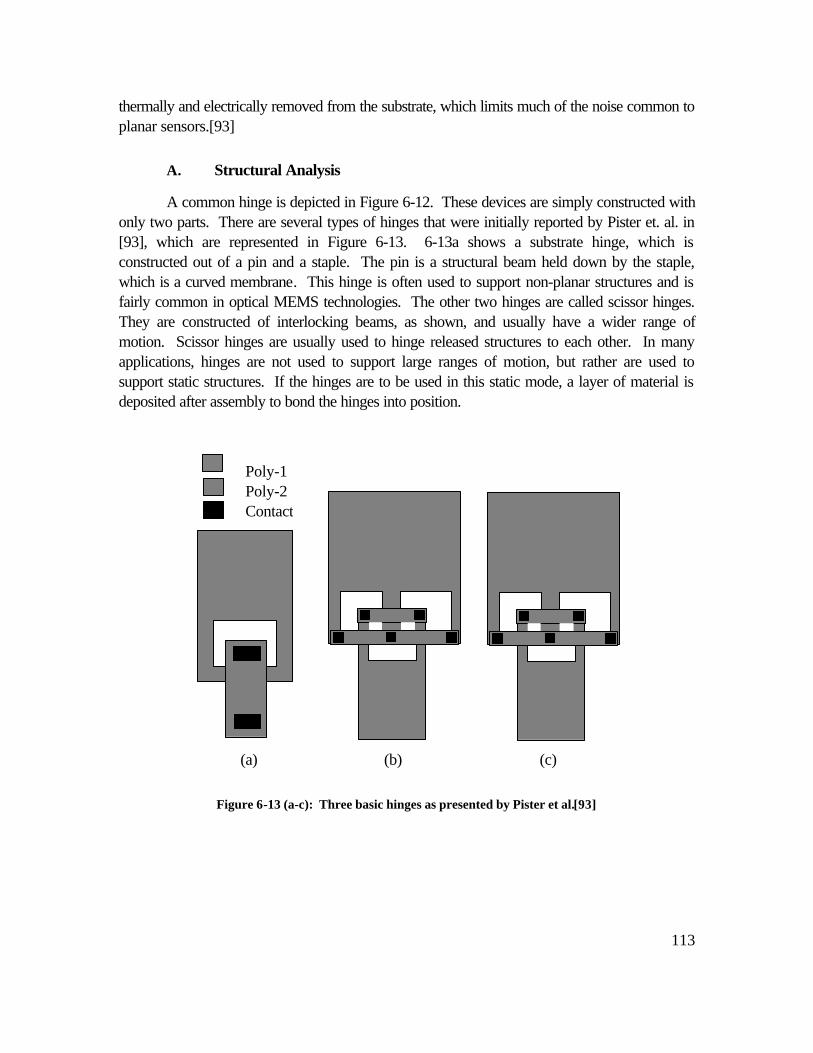
113
thermally and electrically removed from the substrate, which limits much of the noise common toplanar sensors.[93]
A. Structural Analysis
A common hinge is depicted in Figure 6-12. These devices are simply constructed withonly two parts. There are several types of hinges that were initially reported by Pister et. al. in[93], which are represented in Figure 6-13. 6-13a shows a substrate hinge, which isconstructed out of a pin and a staple. The pin is a structural beam held down by the staple,which is a curved membrane. This hinge is often used to support non-planar structures and isfairly common in optical MEMS technologies. The other two hinges are called scissor hinges.They are constructed of interlocking beams, as shown, and usually have a wider range ofmotion. Scissor hinges are usually used to hinge released structures to each other. In manyapplications, hinges are not used to support large ranges of motion, but rather are used tosupport static structures. If the hinges are to be used in this static mode, a layer of material isdeposited after assembly to bond the hinges into position.
Figure 6-13 (a-c): Three basic hinges as presented by Pister et al.[93]
Poly-1Poly-2Contact
(a) (b) (c)
114
B. Reliability Concerns
One of the limitations in designing a substrate hinge is in designing the pin so that it is notwider than the allowable clearance of the staple. While this is an easy enough issue to addressin design, it does provide some upper limits on the strength of the hinge. Scissor hinges, on theother hand, do not have limitations on the width of the beams. As a result scissor hinges areconsidered stronger structures than substrate hinges. If the hinge is anchored in place by thedeposition of material after the device has been assembled, the adhesive strength of thedeposited material will determine the hinge strength. Although Pister et al. reported a PECVDoxide layer that can withstand a torque of 10 nNm, this data would have to be independentlydetermined by individual foundries.
Another area of concern in hinged devices is the issue of assembling hinged devices.While this is commonly done with micromanipulator stages in the laboratory setting, it may beextremely difficult to do this on a reproducible basis on a production line. As a result,membranes that are supported by hinges must be examined for damage caused in the assemblyprocess.
C. Additional Reading
K. S. Pister, M. W. Judy, S. R. Burgett, and R. S. Fearing, “Microfabricated Hinges” Sensorsand Actuators A, Vol. 33, pp. 249-256, 1992.
M. E. Motamedi, M. C. Wu and K. S. Pister, “Micro-opto-electro-mechanical Devices andOn-chip Optical Processing” Optical Engineering, Vol. 36, No. 5, May 1997.
115
IV. Piezoresistive Transducers
Piezoresistivity is the property of a material whereby the bulk resistivity changes underthe influence of a stress field. While all materials have varying degrees of piezoresistiveresponses, piezoresistors are commonly employed in semiconductor sensors because manysemiconductor materials have large piezoresistive responses. The actual physics behindpiezoresistive devices is slightly involved, but necessary to understanding its effects.
A. Formal Definition
To understand piezoresistivity, several other concepts must be first introduced. For athree-dimensional, anisotropic crystal, the electric field is related to a current by a three-by-threeresistivity tensor given below.
⋅
=
z
y
x
z
y
x
ii
i
343
426
561
ρρρρρρ
ρρρ
εε
ε
If a Cartesian coordinate system is aligned to the <100> axis, then ρ4, ρ5, and ρ6
become correlation coefficients, which relate the electric field in one axis to the current in aperpendicular direction. This leads to the result that in an isotropic conductor, such asunstressed silicon, ρ1=ρ2=ρ3=ρ and ρ4=ρ5=ρ6=0. These values can be related to incrementalchanges in resistivity by the following equation:
∆∆∆∆∆
∆
+
=
6
5
4
3
2
1
6
5
4
3
2
1
000
ρρρρρ
ρ
ρρρ
ρρρρρ
ρ
To define the piezoresistivity, all one needs to do is to relate the fractional change inresistivity, ∆ρi/ρ to the stresses in the crystal. In order to do this fully, a 6x6 matrix must bedefined. But for a crystal, this matrix will exhibit the same symmetries as the crystal lattice itself,which will obviate the need for many of the matrix coefficients. If the coefficients are defined asπ ij, a cubic crystal structure will only have three non-vanishing coefficients. For a silicon lattice,the matrix becomes:
(6-32)
(6-33)
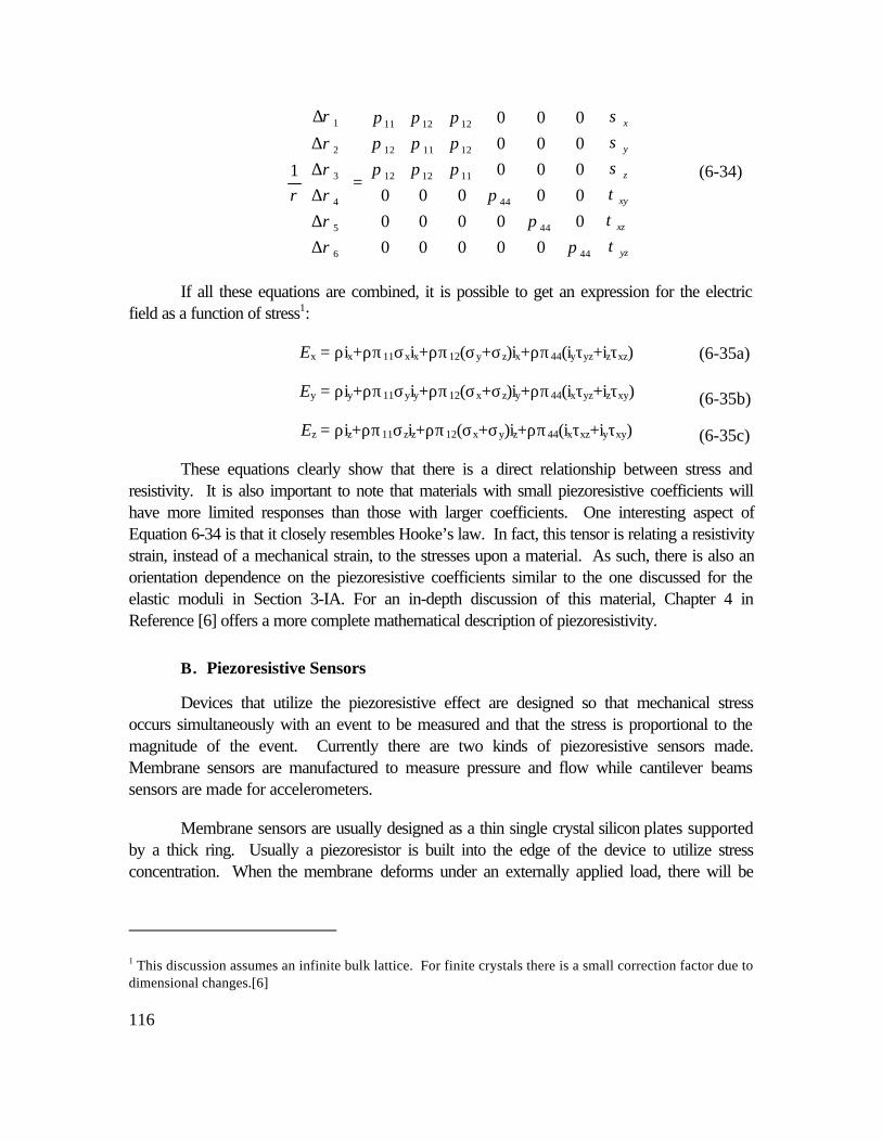
116
=
∆∆∆∆∆
∆
yz
xz
xy
z
y
x
τττσσσ
ππ
ππππππππππ
ρρρρρ
ρ
ρ
44
44
44
111212
121112
121211
6
5
4
3
2
1
000000000000000000000000
1
If all these equations are combined, it is possible to get an expression for the electricfield as a function of stress1:
Ex = ρix+ρπ11σxix+ρπ12(σy+σz)ix+ρπ44(iyτyz+izτxz)
Ey = ρiy+ρπ11σyiy+ρπ12(σx+σz)iy+ρπ44(ixτyz+izτxy)
Ez = ρiz+ρπ11σziz+ρπ12(σx+σy)iz+ρπ44(ixτxz+iyτxy)
These equations clearly show that there is a direct relationship between stress andresistivity. It is also important to note that materials with small piezoresistive coefficients willhave more limited responses than those with larger coefficients. One interesting aspect ofEquation 6-34 is that it closely resembles Hooke’s law. In fact, this tensor is relating a resistivitystrain, instead of a mechanical strain, to the stresses upon a material. As such, there is also anorientation dependence on the piezoresistive coefficients similar to the one discussed for theelastic moduli in Section 3-IA. For an in-depth discussion of this material, Chapter 4 inReference [6] offers a more complete mathematical description of piezoresistivity.
B. Piezoresistive Sensors
Devices that utilize the piezoresistive effect are designed so that mechanical stressoccurs simultaneously with an event to be measured and that the stress is proportional to themagnitude of the event. Currently there are two kinds of piezoresistive sensors made.Membrane sensors are manufactured to measure pressure and flow while cantilever beamssensors are made for accelerometers.
Membrane sensors are usually designed as a thin single crystal silicon plates supportedby a thick ring. Usually a piezoresistor is built into the edge of the device to utilize stressconcentration. When the membrane deforms under an externally applied load, there will be
1 This discussion assumes an infinite bulk lattice. For finite crystals there is a small correction factor due todimensional changes.[6]
(6-34)
(6-35a)
(6-35b)
(6-35c)
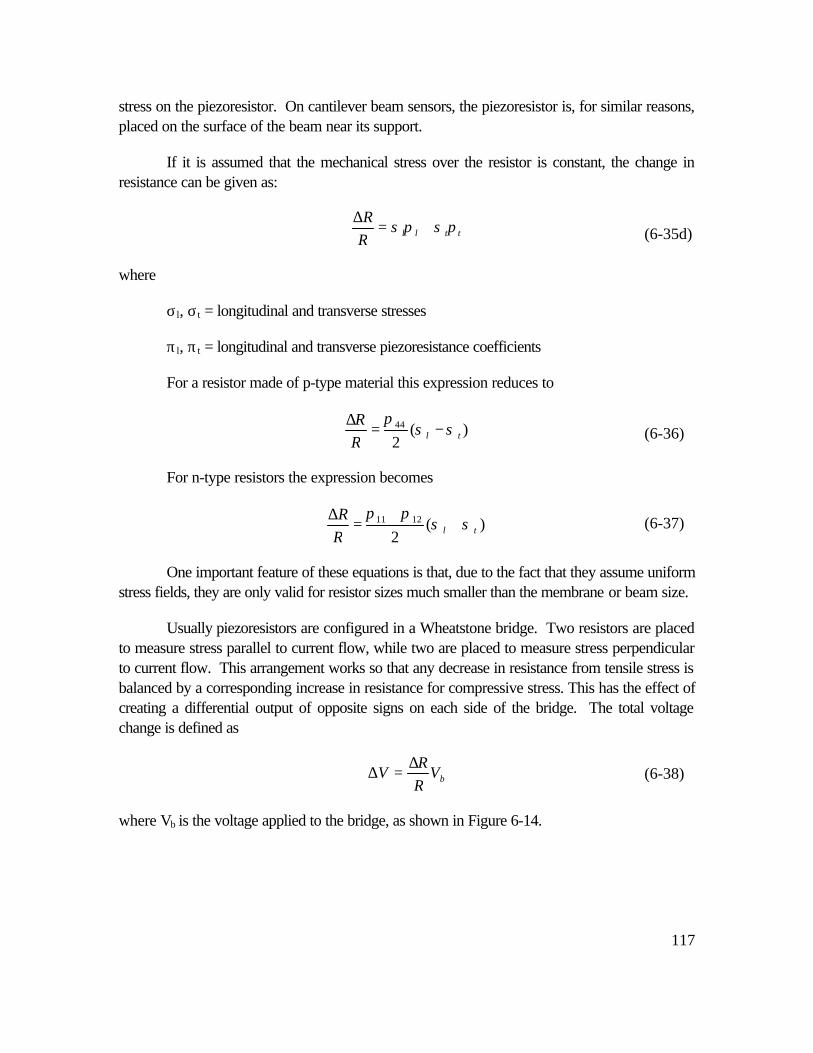
117
stress on the piezoresistor. On cantilever beam sensors, the piezoresistor is, for similar reasons,placed on the surface of the beam near its support.
If it is assumed that the mechanical stress over the resistor is constant, the change inresistance can be given as:
ttllRR
πσπσ +=∆
where
σl, σt = longitudinal and transverse stresses
π l, π t = longitudinal and transverse piezoresistance coefficients
For a resistor made of p-type material this expression reduces to
)(244
tlRR
σσπ
−=∆
For n-type resistors the expression becomes
)(2
1211tlR
Rσσ
ππ+
+=
∆
One important feature of these equations is that, due to the fact that they assume uniformstress fields, they are only valid for resistor sizes much smaller than the membrane or beam size.
Usually piezoresistors are configured in a Wheatstone bridge. Two resistors are placedto measure stress parallel to current flow, while two are placed to measure stress perpendicularto current flow. This arrangement works so that any decrease in resistance from tensile stress isbalanced by a corresponding increase in resistance for compressive stress. This has the effect ofcreating a differential output of opposite signs on each side of the bridge. The total voltagechange is defined as
bVRR
V∆
=∆
where Vb is the voltage applied to the bridge, as shown in Figure 6-14.
(6-35d)
(6-36)
(6-37)
(6-38)
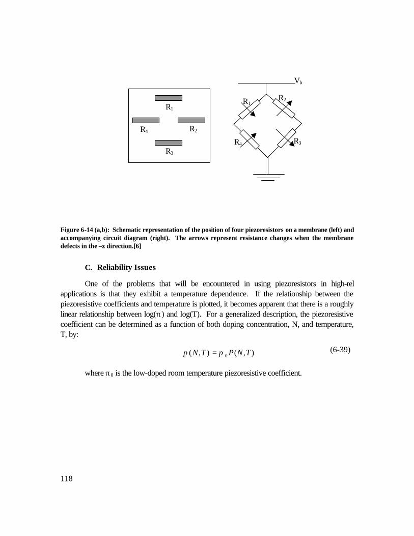
118
Figure 6-14 (a,b): Schematic representation of the position of four piezoresistors on a membrane (left) andaccompanying circuit diagram (right). The arrows represent resistance changes when the membranedefects in the –z direction.[6]
C. Reliability Issues
One of the problems that will be encountered in using piezoresistors in high-relapplications is that they exhibit a temperature dependence. If the relationship between thepiezoresistive coefficients and temperature is plotted, it becomes apparent that there is a roughlylinear relationship between log(π) and log(T). For a generalized description, the piezoresistivecoefficient can be determined as a function of both doping concentration, N, and temperature,T, by:
),(),( 0 TNPTN ππ =
where π0 is the low-doped room temperature piezoresistive coefficient.
R1
R2
R1
R4
R4
R2
R3
R3
Vb
(6-39)
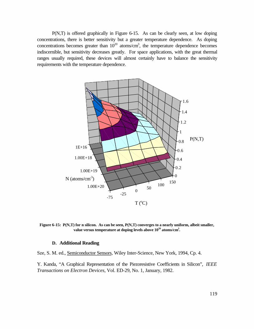
119
P(N,T) is offered graphically in Figure 6-15. As can be clearly seen, at low dopingconcentrations, there is better sensitivity but a greater temperature dependence. As dopingconcentrations becomes greater than 1020 atoms/cm3, the temperature dependence becomesindiscernible, but sensitivity decreases greatly. For space applications, with the great thermalranges usually required, these devices will almost certainly have to balance the sensitivityrequirements with the temperature dependence.
Figure 6-15: P(N,T) for n silicon. As can be seen, P(N,T) converges to a nearly uniform, albeit smaller,value versus temperature at doping levels above 1020 atoms/cm3.
D. Additional Reading
Sze, S. M. ed., Semiconductor Sensors, Wiley Inter-Science, New York, 1994, Cp. 4.
Y. Kanda, “A Graphical Representation of the Piezoresistive Coefficients in Silicon”, IEEETransactions on Electron Devices, Vol. ED-29, No. 1, January, 1982.
1E+16
1.00E+18
1.00E+19
1.00E+20
-75-25
050
100150
0
0.2
0.4
0.6
0.8
1
1.2
1.4
1.6
T (oC)
N (atoms/cm-3)
P(N,T)
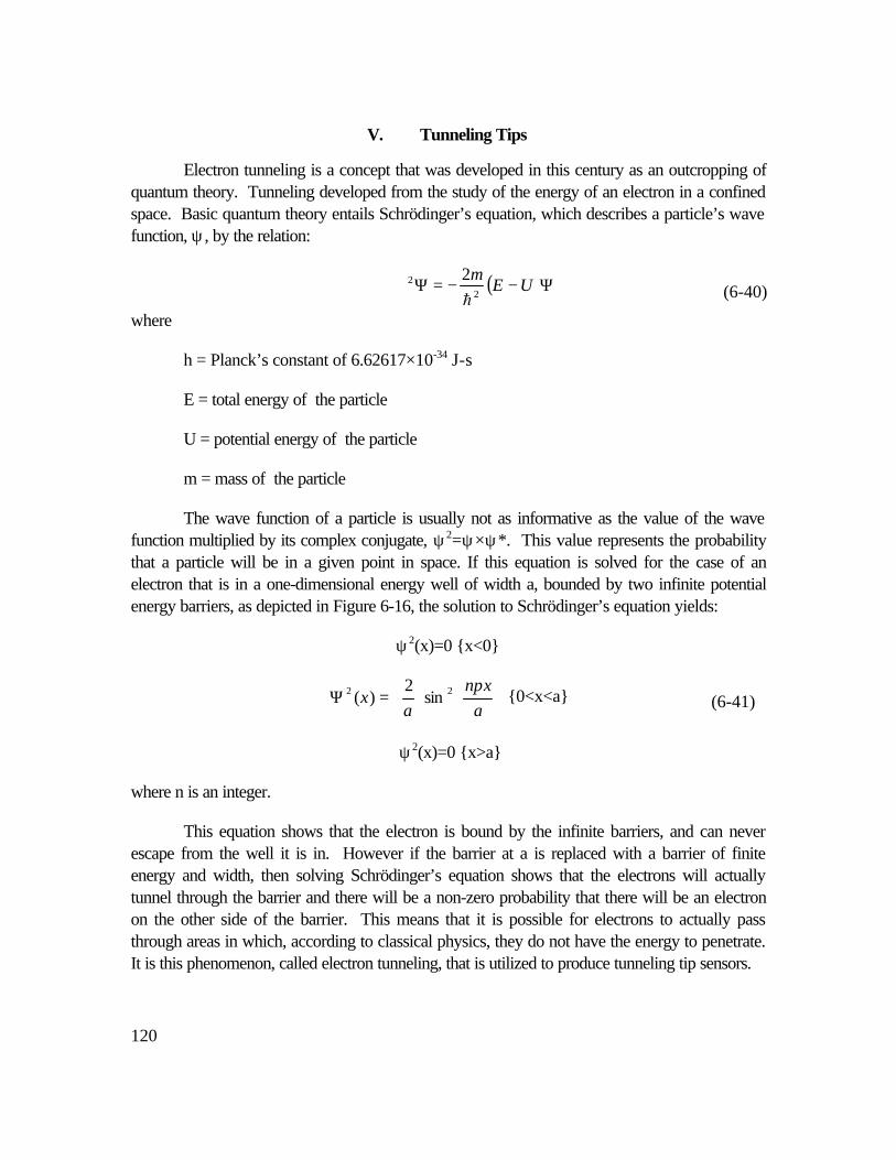
120
V. Tunneling Tips
Electron tunneling is a concept that was developed in this century as an outcropping ofquantum theory. Tunneling developed from the study of the energy of an electron in a confinedspace. Basic quantum theory entails Schrödinger’s equation, which describes a particle’s wavefunction, ψ, by the relation:
( )Ψ−−=Ψ∇ UEm2
2 2h
where
h = Planck’s constant of 6.62617×10⁻³⁴ J-s
E = total energy of the particle
U = potential energy of the particle
m = mass of the particle
The wave function of a particle is usually not as informative as the value of the wavefunction multiplied by its complex conjugate, ψ2=ψ×ψ*. This value represents the probabilitythat a particle will be in a given point in space. If this equation is solved for the case of anelectron that is in a one-dimensional energy well of width a, bounded by two infinite potentialenergy barriers, as depicted in Figure 6-16, the solution to Schrödinger’s equation yields:
ψ2(x)=0 x<0
=Ψ
axn
ax
π22 sin2
)( 0<x<a
ψ2(x)=0 x>a
where n is an integer.
This equation shows that the electron is bound by the infinite barriers, and can neverescape from the well it is in. However if the barrier at a is replaced with a barrier of finiteenergy and width, then solving Schrödinger’s equation shows that the electrons will actuallytunnel through the barrier and there will be a non-zero probability that there will be an electronon the other side of the barrier. This means that it is possible for electrons to actually passthrough areas in which, according to classical physics, they do not have the energy to penetrate.It is this phenomenon, called electron tunneling, that is utilized to produce tunneling tip sensors.
(6-41)
(6-40)
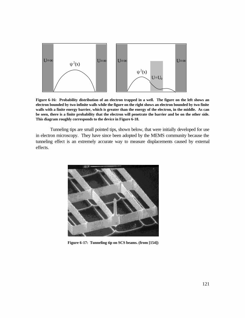
121
Figure 6-16: Probability distribution of an electron trapped in a well. The figure on the left shows anelectron bounded by two infinite walls while the figure on the right shows an electron bounded by two finitewalls with a finite energy barrier, which is greater than the energy of the electron, in the middle. As canbe seen, there is a finite probability that the electron will penetrate the barrier and be on the other side.This diagram roughly corresponds to the device in Figure 6-18.
Tunneling tips are small pointed tips, shown below, that were initially developed for usein electron microscopy. They have since been adopted by the MEMS community because thetunneling effect is an extremely accurate way to measure displacements caused by externaleffects.
Figure 6-17: Tunneling tip on SCS beams. (from [154])
U=∞ U=∞ψ2(x)
U=∞
U=U0
ψ2(x)
U=∞
122
A. Physical Description
It has been shown that the current caused by tunneling across a narrow barrier is givenby:
( )φαxVeI −∝
where
V = bias voltage on the tip
α= 1.025 Å-1ev-1/2
φ = the effective energy height of the tunneling barrier = xV
VI
I ∂∂
∂∂
−α1
x = the physical width of the energy barrier
This means that an electronic circuit capable of detecting a 1% variation in a 1 nAcurrent from a 100 MΩ source would be able to detect deflections on the order of 0.003 Å.For this reason tunneling tips have started to be developed for use in high data storageapplications and high sensitivity accelerometers.
Typically tunneling sensors are designed by suspending a mass above the tunnelingsensor. An external force, which can be anything from infrared radiation to acceleration, pushesthe mass downwards, which increases the tunneling current and becomes a measurable event, asshown in the diagram below.
(6-42)
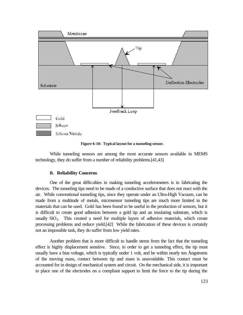
123
While tunneling sensors are among the most accurate sensors available in MEMStechnology, they do suffer from a number of reliability problems.[41,43]
B. Reliability Concerns
One of the great difficulties in making tunneling accelerometers is in fabricating thedevices. The tunneling tips need to be made of a conductive surface that does not react with theair. While conventional tunneling tips, since they operate under an Ultra-High Vacuum, can bemade from a multitude of metals, microsensor tunneling tips are much more limited in thematerials that can be used. Gold has been found to be useful in the production of sensors, but itis difficult to create good adhesion between a gold tip and an insulating substrate, which isusually SiO2. This created a need for multiple layers of adhesive materials, which createprocessing problems and reduce yield.[42] While the fabrication of these devices is certainlynot an impossible task, they do suffer from low yield rates.
Another problem that is more difficult to handle stems from the fact that the tunnelingeffect is highly displacement sensitive. Since, in order to get a tunneling effect, the tip mustusually have a bias voltage, which is typically under 1 volt, and be within nearly ten Ångstromsof the moving mass, contact between tip and mass is unavoidable. This contact must beaccounted for in design of mechanical system and circuit. On the mechanical side, it is importantto place one of the electrodes on a compliant support to limit the force to the tip during the
Figure 6-18: Typical layout for a tunneling sensor.
124
inevitable contact. The circuit must also limit the current during contact. If both of theseprecautions are taken, the danger of tip crashes will be mitigated. For devices designed withthese techniques, crashes have occurred at low frequency operation for months with nodetectable change in operational characteristics. However, any tunneling tip designs need tohave these issues thoroughly addressed for high-rel applications.
These devices, due to their extreme sensitivity, are also susceptible to thermal noise andmechanical vibration. It is typically these effects that limit device sensitivity and they need to beaddressed for any tunneling sensor. There is also electrical noise in the measurements of thetunneling output. In many devices, the electrical noise spectrum exhibits a 1/f dependence. Thisnoise creates an error in measurements that scales on the order of 10-3 Å/Hz½. While this noiseis fairly insignificant for many applications, it does provide a limit on the actual sensitivity of thedevice.[41]
C. Additional Reading
T. W. Kenny, W. J. Kaiser, H. K. Rockstad, J. K. Reynolds, J. A. Podosek, and E. C. Vote,“Wide-Bandwidth Electromechanical Actuators for Tunneling Displacement Transducers”Journal of Microelectromechanical Systems, Vol. 3. No. 3, September 1994.
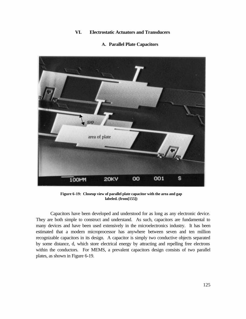
125
VI. Electrostatic Actuators and Transducers
A. Parallel Plate Capacitors
Capacitors have been developed and understood for as long as any electronic device.They are both simple to construct and understand. As such, capacitors are fundamental tomany devices and have been used extensively in the microelectronics industry. It has beenestimated that a modern microprocessor has anywhere between seven and ten millionrecognizable capacitors in its design. A capacitor is simply two conductive objects separatedby some distance, d, which store electrical energy by attracting and repelling free electronswithin the conductors. For MEMS, a prevalent capacitors design consists of two parallelplates, as shown in Figure 6-19.
Figure 6-19: Closeup view of parallel plate capacitor with the area and gaplabeled. (from[155])
area of plate
gap

126
i) Electrical and Mechanical Analysis
The capacitance of an object is defined as the amount of electric charge that it can storeper voltage. The common mathematical expression of a capacitor’s ability to store energy orcharge is related by the expressions:
q = CV
U = ½CV2
where
q = electric charge
V = voltage
C = capacitance
U = energy
For capacitors constructed of two parallel plates a useful relationship has been derivedthat:
dA
C ε=
where
A = area of one of the plates
d = distance between the plates
ε = the permittivity of the material between the two plates
One reason that capacitors have become prevalent in MEMS is that capacitance is afunction of distance. This means that a change in distance will result in a change in capacitance,which is a measurable event. If a capacitor immersed in air is assumed to have one fixed plateand one plate that displaces a distance, x, from the rest, the capacitance can be rewritten as:
)(0 xdA
C−
= ε
where
ε0 = permittivity of a free space (8.85*10-12 F/m)
(6-43a)
(6-43b)
(6-44)
(6-45)
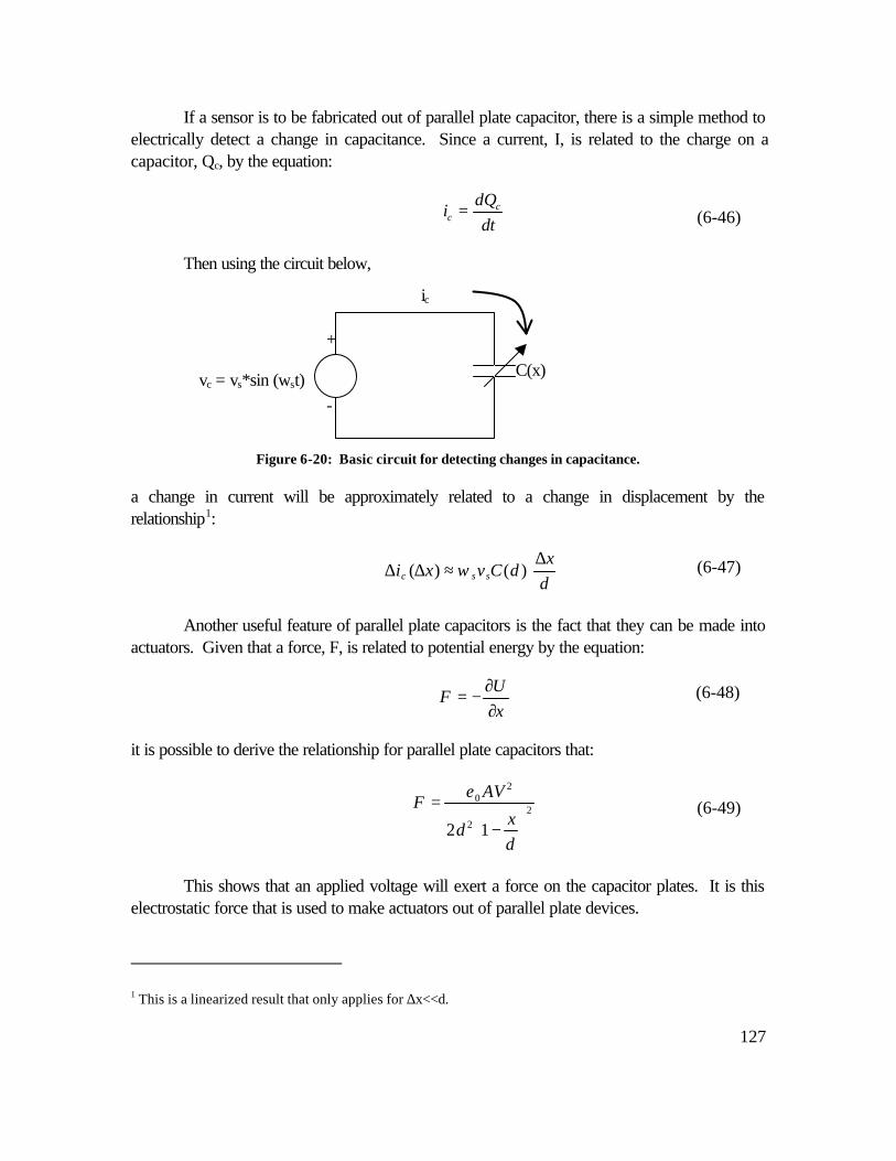
127
If a sensor is to be fabricated out of parallel plate capacitor, there is a simple method toelectrically detect a change in capacitance. Since a current, I, is related to the charge on acapacitor, Qc, by the equation:
dtdQ
i cc =
Then using the circuit below,
Figure 6-20: Basic circuit for detecting changes in capacitance.
a change in current will be approximately related to a change in displacement by therelationship1:
∆
≈∆∆dx
dCvxi ssc )()( ω
Another useful feature of parallel plate capacitors is the fact that they can be made intoactuators. Given that a force, F, is related to potential energy by the equation:
xU
F∂∂
−=
it is possible to derive the relationship for parallel plate capacitors that:
22
20
12
−
=
dx
d
AVF
ε
This shows that an applied voltage will exert a force on the capacitor plates. It is thiselectrostatic force that is used to make actuators out of parallel plate devices.
1 This is a linearized result that only applies for ∆x<<d.
vc = vs*sin (wst)C(x)
ic
+
-
(6-46)
(6-47)
(6-48)
(6-49)
128
ii) Limitations of Parallel Plate Capacitors
While parallel plate capacitors have good actuation and sensing abilities, they have somesevere limitations. The greatest drawback to using these devices is that they are non-linear.While they can be treated as linear for small displacements, for large motions, parallel platecapacitors clearly exhibit non-linear behavior.
One of the dangers in these devices is the potential of the plates touching. As discussedin Chapter 3, when two metal surfaces come into contact, adhesive forces exert a strong bondthat usually causes failure. This problem is especially prevalent in parallel plate devices becauseof the non-linear force that increases quadratically with distance. A common design rule used isthat, if ∆x ≥ 1/3 d, the device will usually have sufficient force to transverse d. To prevent this,parallel plate devices must be designed to displace much less than this amount.[10]
Parallel plate capacitors could also be susceptible to electrostatic discharge. An ESDwould have a similar effect as applying a delta function to the device. If the voltage spike islarge enough, it could induce stiction by bringing the plates into contact. Unfortunately the scantresearch into ESD in MEMS has not provided any concrete data on the effects of ESD onparallel plate capacitors and these theories have not been experimentally verified.
iii) Additional Reading
W. S. Trimmer, K. J. Gabriel, and R. Mahadevan, “Silicon Electrostatic Motors”, Transducers’87, The 4th International Conference of Solid-State Sensors and Actuators, pp. 857-860,June 1987.
W. S. Trimmer and K. J. Gabriel, “Design Considerations for a Practical Electrostatic Micro-Motor”, Sensors and Actuators, Vol. 11, pp. 189-206, 1987.

129
B. Comb Drives
Due to the problems discussed with making electrostatic parallel plate actuators, therehave been attempts made to make devices that utilize electrostatics to produce motion whileeliminating the relationship between force and distance. The most common device made toaccomplish this is called a comb drive because of its overall comb-like appearance, as seen inFigure 6-16. Comb drives operate by using fringing fields to pull one set of the drive into theother. Actuation occurs in one dimension only and the equations of motion are derived in thenext section.
i) Mechanical and Electrical Analysis
Essentially comb drives are composed of multiple structural beams and, as such, theyare not difficult to analyze. As shown in the picture, there are two sets of interdigitatedelectrodes. Generally one of them is fixed while the other is mobile. The force generated by avoltage is described by:
Figure 6-21: A standard comb drive. The arrow points to a particulate that landedon one of the electrodes.

130
dbV
F2
0ε=
where b is the vertical height of the cantilever beams.
This equation shows that the force produced by this device is independent of thedisplacement of the middle electrode. As a result, comb drives are among the more commonactuators in MEMS. The other fact that makes comb drives appealing is that n comb drivesproduce a force equal to n×F. This simple scaling makes it possible to produce macroscopicforces on the MEMS scale. It is not unreasonable to manufacture an array of comb drives toproduce upwards of 30 Newtons with as little as 10 volts applied to the electrodes.[10] Whilethese aspects of comb drives are quite appealing, there are also some serious limitations to theirperformance.
ii) Limitations on Design
One of the problems with comb drives illustrated by Figure 6-22 is that there is oneelectrode. For argument’s sake, assume it to be negatively charged, surrounded by twopositively charged electrodes. While the forces on the electrode are balanced by the equalspacing of the two gaps, clearly any perturbation of the center electrode will cause an offset ofthe forces and pull the electrode to one side or another. In engineering terms, the comb drive isan inherently unstable system. To combat this problem, several steps must be taken in thedesign to insure that the device does not fail at the first vibration. Since stability problems areproblems in energy storage, the key to designing a stable comb drive is to design it to storemore energy in the y direction than in the x direction. To make Uy >> Ux, the followingcondition must be met:
yX
Figure 6-22: Overhead view of basic unit of a comb drive.
- - - - - - - - - - - -
+ + + + + + + + + +
+ + + + + + + + + +
+ + + + + + +
Fd
x
(6-50)
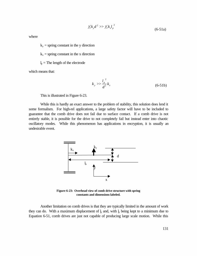
131
22
122
1pxy lkdk >>
where
ky = spring constant in the y direction
kx = spring constant in the x direction
lp = The length of the electrode
which means that:
xp
y kd
lk 2
2
>>
This is illustrated in Figure 6-23.
While this is hardly an exact answer to the problem of stability, this solution does lend itsome formalism. For high-rel applications, a large safety factor will have to be included toguarantee that the comb drive does not fail due to surface contact. If a comb drive is notentirely stable, it is possible for the drive to not completely fail but instead enter into chaoticoscillatory modes. While this phenomenon has applications in encryption, it is usually anundesirable event.
Another limitation on comb drives is that they are typically limited in the amount of workthey can do. With a maximum displacement of lp and, with lp being kept to a minimum due toEquation 6-51, comb drives are just not capable of producing large scale motion. While this
ky kx
y
x
lp
d
Figure 6-23: Overhead view of comb drive structure with springconstants and dimensions labeled.
kykx
(6-51a)
(6-51b)

132
problem can be designed around to a degree, it is nevertheless a serious limitation to comb driveusage.
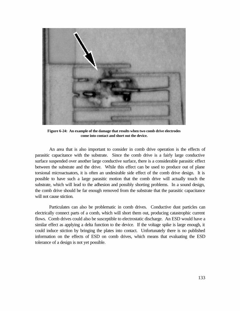
133
An area that is also important to consider in comb drive operation is the effects ofparasitic capacitance with the substrate. Since the comb drive is a fairly large conductivesurface suspended over another large conductive surface, there is a considerable parasitic effectbetween the substrate and the drive. While this effect can be used to produce out of planetorsional microactuators, it is often an undesirable side effect of the comb drive design. It ispossible to have such a large parasitic motion that the comb drive will actually touch thesubstrate, which will lead to the adhesion and possibly shorting problems. In a sound design,the comb drive should be far enough removed from the substrate that the parasitic capacitancewill not cause stiction.
Particulates can also be problematic in comb drives. Conductive dust particles canelectrically connect parts of a comb, which will short them out, producing catastrophic currentflows. Comb drives could also be susceptible to electrostatic discharge. An ESD would have asimilar effect as applying a delta function to the device. If the voltage spike is large enough, itcould induce stiction by bringing the plates into contact. Unfortunately there is no publishedinformation on the effects of ESD on comb drives, which means that evaluating the ESDtolerance of a design is not yet possible.
Figure 6-24: An example of the damage that results when two comb drive electrodescome into contact and short out the device.

134
iii) Additional Reading
W. C. Tang, T.-C. H. Nguyen, and R. T. Howe, “Laterally Driven Polysilicon ResonantMicrostructures.” Proceedings of IEEE Microelectromechanical Systems, February 1989.
W. C. Tang, T.-C. H. Nguyen, M. W. Judy and R. T. Howe, “Electrostatic-comb Drive ofLateral Polysilicon Resonators” Transducers ’89, Proceedings of the 5th InternationalConference on Solid-State Sensors and Actuators and Eurosensors III, Vol. 2, pp. 328-331, June 1990.
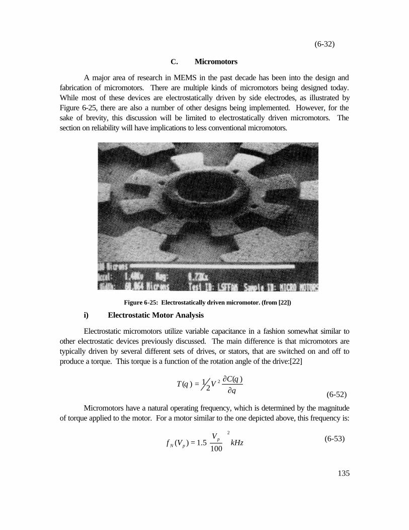
135
C. Micromotors
A major area of research in MEMS in the past decade has been into the design andfabrication of micromotors. There are multiple kinds of micromotors being designed today.While most of these devices are electrostatically driven by side electrodes, as illustrated byFigure 6-25, there are also a number of other designs being implemented. However, for thesake of brevity, this discussion will be limited to electrostatically driven micromotors. Thesection on reliability will have implications to less conventional micromotors.
i) Electrostatic Motor Analysis
Electrostatic micromotors utilize variable capacitance in a fashion somewhat similar toother electrostatic devices previously discussed. The main difference is that micromotors aretypically driven by several different sets of drives, or stators, that are switched on and off toproduce a torque. This torque is a function of the rotation angle of the drive:[22]
θθ
θ∂
∂=
)(2
1)( 2 CVT
Micromotors have a natural operating frequency, which is determined by the magnitudeof torque applied to the motor. For a motor similar to the one depicted above, this frequency is:
kHzV
Vf ppN
2
1005.1)(
=
Figure 6-25: Electrostatically driven micromotor. (from [22])
(6-52)
(6-32)
(6-53)
136
where Vp is the phase voltage applied to the stators. This leads to an equation for the maximumrotational speed of the motor, ωmax:
rpmn
fN240max =ω
where n is the number of steps per revolution determined by1:
−
=
rs nn
n11
1
where ns and nr are the respective numbers of stators and rotors.
These motors can be either used as microstepper motors or can be operated as acontinuously rotating motor. While the actual design and fabrication of these devices variesdepending upon application, most electrostatic motors are governed by the above physicallaws.[22,23]
ii) Harmonic Motors
Harmonic motors are a kind of motor that utilizes the rolling motion of two bodies withdifferent circumferences. Typically a motor contains a cylindrical hole, with a slightly smallercylindrical rotor. These motors have a tribological interest as they utilize rolling instead of slidingfriction, which eliminates many of the wear concerns common to other motors. Furthermore,since the stators and rotors are designed to touch in these devices, large amounts of force canbe generated.
Using one of the original harmonic motors as an example, there are some basic facts ofmotor operation that are fairly common to all harmonic motors. If the stators are cycled at afrequency of ωs, then it is possible to determine the steady state frequency of the harmonicmotor, ωr:[87]
−= 1
r
ssr R
Rωω
where Rs and Rr are dimensions defined in Figure 6-24.
1 This derivation assumes a drive signal described by Y. –C. Tai et al. in [22].
(6-54)
(6-55)
(6-56)
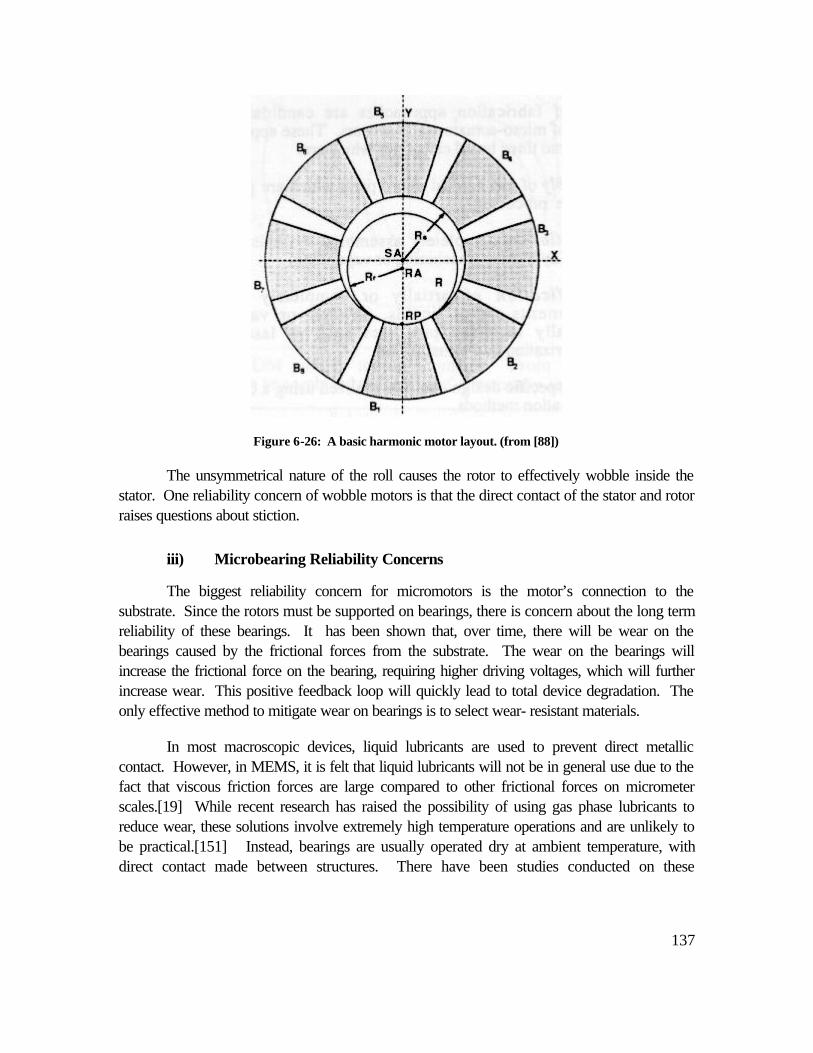
137
Figure 6-26: A basic harmonic motor layout. (from [88])
The unsymmetrical nature of the roll causes the rotor to effectively wobble inside thestator. One reliability concern of wobble motors is that the direct contact of the stator and rotorraises questions about stiction.
iii) Microbearing Reliability Concerns
The biggest reliability concern for micromotors is the motor’s connection to thesubstrate. Since the rotors must be supported on bearings, there is concern about the long termreliability of these bearings. It has been shown that, over time, there will be wear on thebearings caused by the frictional forces from the substrate. The wear on the bearings willincrease the frictional force on the bearing, requiring higher driving voltages, which will furtherincrease wear. This positive feedback loop will quickly lead to total device degradation. Theonly effective method to mitigate wear on bearings is to select wear- resistant materials.
In most macroscopic devices, liquid lubricants are used to prevent direct metalliccontact. However, in MEMS, it is felt that liquid lubricants will not be in general use due to thefact that viscous friction forces are large compared to other frictional forces on micrometerscales.[19] While recent research has raised the possibility of using gas phase lubricants toreduce wear, these solutions involve extremely high temperature operations and are unlikely tobe practical.[151] Instead, bearings are usually operated dry at ambient temperature, withdirect contact made between structures. There have been studies conducted on these
138
conditions and it has been found that different materials respond, as would be expected, indistinct ways to wear.
Several studies[19,153] indicate that single crystal silicon is moderately well suited as abearing material. During initial burn-in, the rough points in a bearing will fracture off, leaving asmoothed surface that shows little wear over time. As a result, the wear on silicon decreaseswith time. Polysilicon shows moderate wear properties and is a suitable, although not ideal,bearing material. As would be expected, Si3N4 and SiO2 exhibit poor bearing characteristics.They show linear wear that leads to total failure. Diamond-like carbon is a material that hasshown promise as a bearing material and may eventually be used as a coating on many SCS andpolysilicon structures that have large contact stresses. While the exact characteristics of bearingwear are dependent upon the materials involved and the environment in which they slide, a goodrule of thumb is that wear is minimized by using dissimilar hard materials
Another problem associated with wear on microbearings is that, for electrostaticallydriven structures, forces on the device will be a function of the device height, and thus bearingheight. Many devices place rotors above stators in order to have a non planar component offorce to partially levitate the rotor. As the bearings wear, the electrode distance woulddecrease, which would cause forces to increase quadratically. This increases wear and altersdrive performance. This behavior accelerates failure and leads to total device collapse.Ultimately, the contact morphologies of microbearings are the limiting factor in micromotorperformance and, as such, they need to be well understood for high-rel applications.
iv) Additional Reading
Long-Sheng Fan, Yu-Chong Tai, and Richard S. Muller, “IC-Processed ElectrostaticMicromotors.” IEEE International Electronic Devices Meeting, December 1988.
Yu-Chong Tai, Long-Sheng Fan, and Richard S. Muller, “IC-Processed Micromotors: Design,Technology, and Testing” Proceedings of IEEE Microelectromechanical Systems, February1989.
U. Beerschwinger, D. Mathieson, R. L. Reuben, and S. J. Yang. “A study of Wear on MEMSContact morphologies” Journal of Micromechanics and Microengineering, 7 September1994.
S. C. Jacobsen, R. H. Price, J. E. Wood, T. H. Rytting, and M. Rafaelof, “The Wobble Motor:An Electrostatic, Planetary Armature, Microactuator” Proceedings of IEEEMicroelectromechanical Systems, pp. 17-24, February 1989.
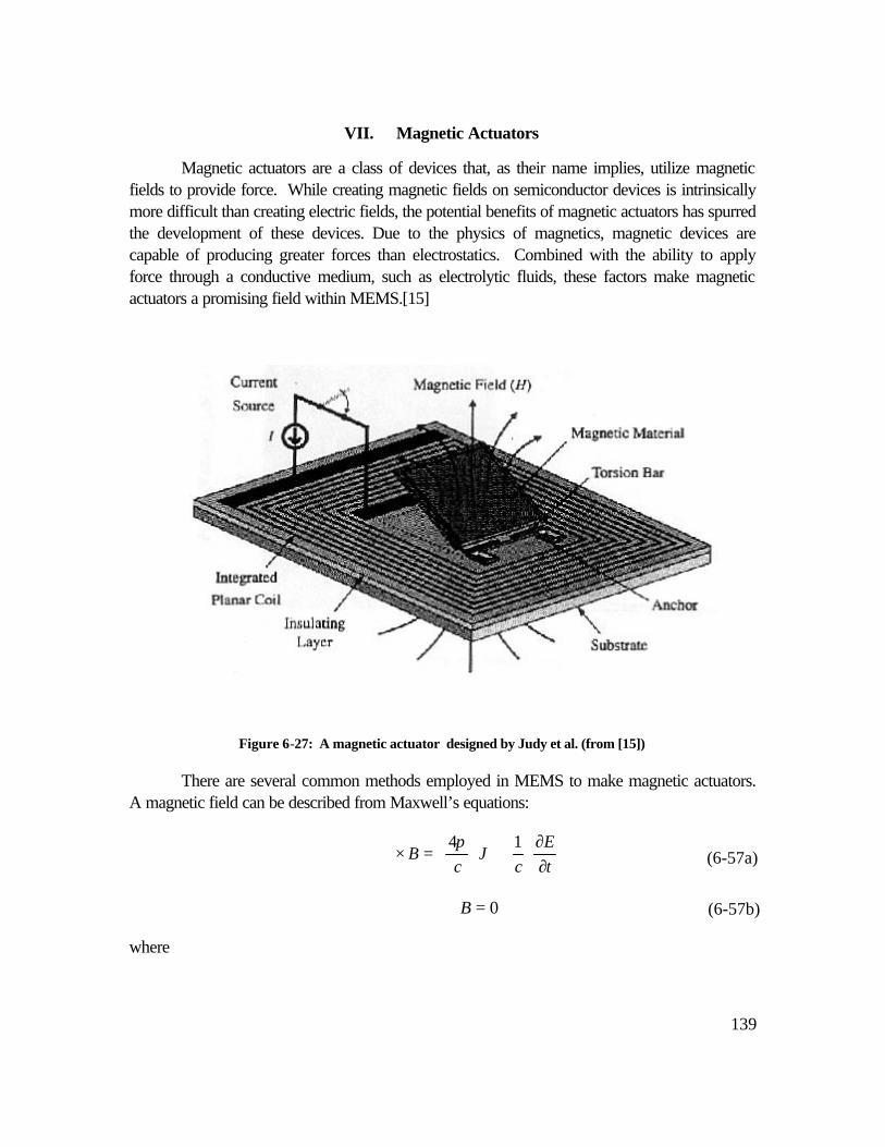
139
VII. Magnetic Actuators
Magnetic actuators are a class of devices that, as their name implies, utilize magneticfields to provide force. While creating magnetic fields on semiconductor devices is intrinsicallymore difficult than creating electric fields, the potential benefits of magnetic actuators has spurredthe development of these devices. Due to the physics of magnetics, magnetic devices arecapable of producing greater forces than electrostatics. Combined with the ability to applyforce through a conductive medium, such as electrolytic fluids, these factors make magneticactuators a promising field within MEMS.[15]
Figure 6-27: A magnetic actuator designed by Judy et al. (from [15])
There are several common methods employed in MEMS to make magnetic actuators.A magnetic field can be described from Maxwell’s equations:
tE
cJ
cB
∂∂
+
=×∇14π
0=⋅∇ B
where
(6-57a)
(6-57b)
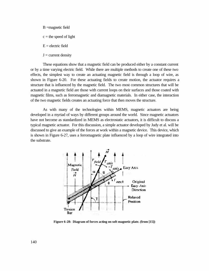
140
B =magnetic field
c = the speed of light
E = electric field
J = current density
These equations show that a magnetic field can be produced either by a constant currentor by a time varying electric field. While there are multiple methods to create one of these twoeffects, the simplest way to create an actuating magnetic field is through a loop of wire, asshown in Figure 6-20. For these actuating fields to create motion, the actuator requires astructure that is influenced by the magnetic field. The two most common structures that will beactuated in a magnetic field are those with current loops on their surfaces and those coated withmagnetic films, such as ferromagnetic and diamagnetic materials. In either case, the interactionof the two magnetic fields creates an actuating force that then moves the structure.
As with many of the technologies within MEMS, magnetic actuators are beingdeveloped in a myriad of ways by different groups around the world. Since magnetic actuatorshave not become as standardized in MEMS as electrostatic actuators, it is difficult to discuss atypical magnetic actuator. For this discussion, a simple actuator developed by Judy et al. will bediscussed to give an example of the forces at work within a magnetic device. This device, whichis shown in Figure 6-27, uses a ferromagnetic plate influenced by a loop of wire integrated intothe substrate.
Figure 6-28: Diagram of forces acting on soft magnetic plate. (from [15])

141
A. Mechanical and Electrical Analysis
For this non-planar magnetic microactuator, the rotational deflection is a function of themagnetic field, H, and the stiffness of the torsion bar, kφ. Assuming that the magnetic fieldremains perpendicular to the original orientation of the plate, the torque produced by themagnetic field, Tfield is defined by:
)cos)2sin(( φπftHHMVT acdcmagfield +=
where
M = net magnetization vector
Vmag = magnetic volume
Hdc, Hac = magnetic field from respective dc and ac sources
f = ac current frequency
φ = angle plate rotates from rest.
To determine the actual mechanical response of the plate, it is necessary to use thedynamic torsional model of
fieldTkCJ =++ φφφ φφ&&&
where
Cφ = dampening coefficient = Q
Jkφ
J = polar moment of inertia of the magnetic plate
Q = quality factor
To determine φ as a function of time, Equation 6-59 must be solved. This can be doneeither analytically or numerically, although the analytic solutions might be difficult to obtain. Inorder to do either, M must be defined, which is done below:
M
ac
NHH
M)(0 +±
=µ
where
(6-58)
(6-59)
(6-60)
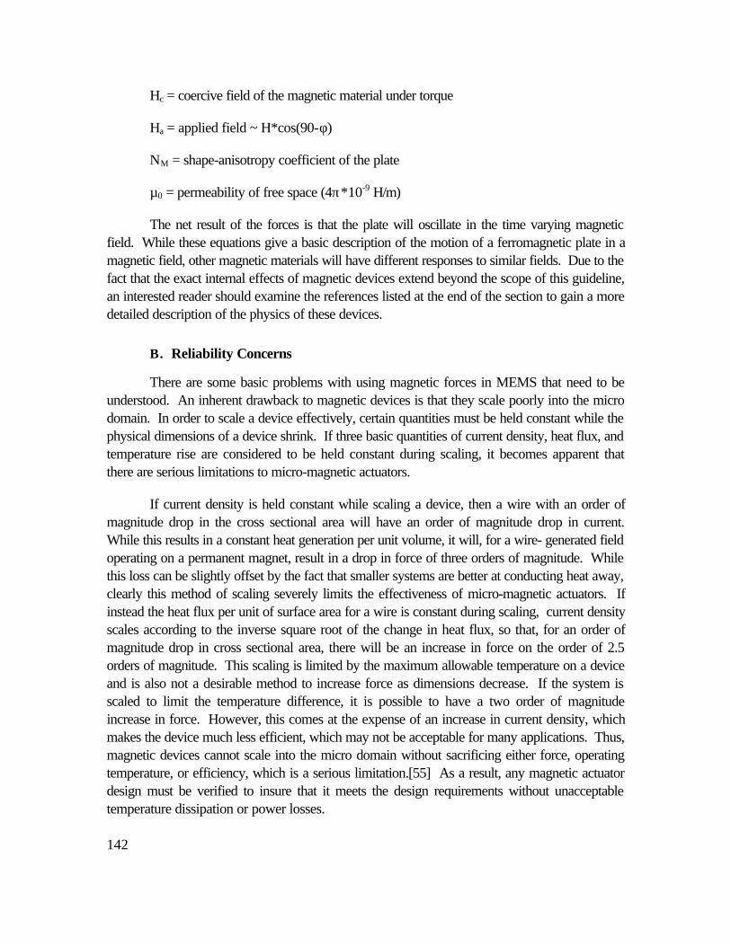
142
Hc = coercive field of the magnetic material under torque
Ha = applied field ~ H*cos(90-φ)
NM = shape-anisotropy coefficient of the plate
µ0 = permeability of free space (4π*10-9 H/m)
The net result of the forces is that the plate will oscillate in the time varying magneticfield. While these equations give a basic description of the motion of a ferromagnetic plate in amagnetic field, other magnetic materials will have different responses to similar fields. Due to thefact that the exact internal effects of magnetic devices extend beyond the scope of this guideline,an interested reader should examine the references listed at the end of the section to gain a moredetailed description of the physics of these devices.
B. Reliability Concerns
There are some basic problems with using magnetic forces in MEMS that need to beunderstood. An inherent drawback to magnetic devices is that they scale poorly into the microdomain. In order to scale a device effectively, certain quantities must be held constant while thephysical dimensions of a device shrink. If three basic quantities of current density, heat flux, andtemperature rise are considered to be held constant during scaling, it becomes apparent thatthere are serious limitations to micro-magnetic actuators.
If current density is held constant while scaling a device, then a wire with an order ofmagnitude drop in the cross sectional area will have an order of magnitude drop in current.While this results in a constant heat generation per unit volume, it will, for a wire- generated fieldoperating on a permanent magnet, result in a drop in force of three orders of magnitude. Whilethis loss can be slightly offset by the fact that smaller systems are better at conducting heat away,clearly this method of scaling severely limits the effectiveness of micro-magnetic actuators. Ifinstead the heat flux per unit of surface area for a wire is constant during scaling, current densityscales according to the inverse square root of the change in heat flux, so that, for an order ofmagnitude drop in cross sectional area, there will be an increase in force on the order of 2.5orders of magnitude. This scaling is limited by the maximum allowable temperature on a deviceand is also not a desirable method to increase force as dimensions decrease. If the system isscaled to limit the temperature difference, it is possible to have a two order of magnitudeincrease in force. However, this comes at the expense of an increase in current density, whichmakes the device much less efficient, which may not be acceptable for many applications. Thus,magnetic devices cannot scale into the micro domain without sacrificing either force, operatingtemperature, or efficiency, which is a serious limitation.[55] As a result, any magnetic actuatordesign must be verified to insure that it meets the design requirements without unacceptabletemperature dissipation or power losses.
143
Another issue to consider in using magnetic actuators aboard spacecraft is the presenceof spurious magnetic fields. Since modern spacecraft employ an array of electronic devices thatcreate magnetic fields, these devices can be unintentionally actuated by nearby devices. A goodmodel of the magnetic fields in a spacecraft, which is usually developed by the systemsengineers, will determine the risk level for parasitic actuation.
C. Additional Reading
R. E. Pelrine, “Room Temperature, Open-Loop Levitation of Microdevices Using DiamagneticMaterials”, Proceedings of IEEE Microelectromechanical Systems, pp. 34-37, February1990.
R. E. Pelrine and I. Busch-Vishniac “Magnetically Levitated Micromachines”, IEEE MicroRobots and Teleoperators, November 1987.
J. W. Judy and R. S. Muller, “Magnetic Microactuation of Torsional Polysilicon Structures,”Sensors and Actuators A, Physical, Vol. A53, Nos. 1-3, pp. 392-397, 1996.
J. W. Judy and R. S. Muller, “Magnetically Actuated, Addressable Microstructures”, Journalof Microelectromechanical Systems, Vol. 6, No. 3, September 1997.
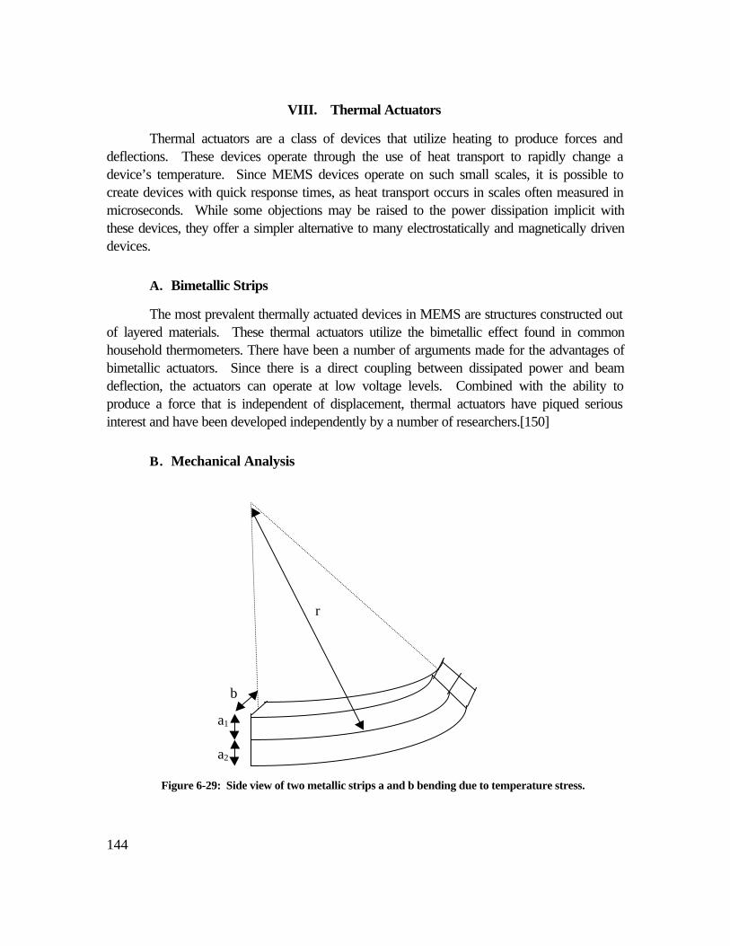
144
VIII. Thermal Actuators
Thermal actuators are a class of devices that utilize heating to produce forces anddeflections. These devices operate through the use of heat transport to rapidly change adevice’s temperature. Since MEMS devices operate on such small scales, it is possible tocreate devices with quick response times, as heat transport occurs in scales often measured inmicroseconds. While some objections may be raised to the power dissipation implicit withthese devices, they offer a simpler alternative to many electrostatically and magnetically drivendevices.
A. Bimetallic Strips
The most prevalent thermally actuated devices in MEMS are structures constructed outof layered materials. These thermal actuators utilize the bimetallic effect found in commonhousehold thermometers. There have been a number of arguments made for the advantages ofbimetallic actuators. Since there is a direct coupling between dissipated power and beamdeflection, the actuators can operate at low voltage levels. Combined with the ability toproduce a force that is independent of displacement, thermal actuators have piqued seriousinterest and have been developed independently by a number of researchers.[150]
B. Mechanical Analysis
a1
a2
r
Figure 6-29: Side view of two metallic strips a and b bending due to temperature stress.
b
145
In these devices, two materials, often Si-SiO 2 or Si-Si3N4 are sandwiched together. Asthe device heats up, the differing changes in length caused by mismatched thermal expansioncoefficient create stresses at the metallurgical junction, which bends the device. Figure 6-29illustrates a bimetallic strip made of two cantilevered beams of lengths l that are exposed to atemperature change, ∆T.
The conversion factor γ, relates a temperature change, ∆T, with a deflection at the endof the cantilever, d, by:
Td ∆= γ
If a uniform heat distribution is assumed with the beams, then the conversion factor canbe approximated for l << r as
Trl∆
=2
2
γ
where r is the radius of curvature of the beam:
( )
)()(
247
32
2121
111
3222
222
3111
212
21
aaTabEabE
abEabE
ttaar
+∆−
++−+=
αα
where α is the linear coefficient of thermal expansion.
A closer mathematical analysis of this equation will show that it is minimized when thecantilever beams have identical values of b and a. For these beams, the deflection is given by:
( )
++
∆−=
χχ
αα
2
21
15
3 Ta
r
where χ is the ratio 2
1
EE
.
Since the absolute width of a structure does not influence bending, the smallest radius ofcurvature, and thus the greatest deflection, will occur if (α1-α2) and l are maximized, while a isminimized. The simplest method to accomplish this comes through altering l and a, as there areonly a few materials, and accompanying thermal expansion coefficients, to choose from in thesemiconductor industry.[149]
As this derivation shows, the displacement of the strip is directly related to a change intemperature. There are several ways to induce temperature changes. One common method is
(6-61)
(6-62)
(6-63)
(6-64)

146
to apply an electric current through the beam. The power dissipated by the current flowingthrough a resistor will produce a ∆T. The amount of energy needed to raise temperature isdetermined by the heat capacity of the cantilever beams. In static operation, it is desirable toreduce all the dimensions of the actuator so that there is less thermal loss. In dynamic operation,as is the case for a high frequency switch, it is more useful to have larger surface areas with agreater heat exchange and a corollary increase in switching rate.[52]
C. Shape Memory Alloys
Shape memory alloy, or SMA, actuators are variants upon thermal actuators that usethe shape memory alloy effect, which was first discovered in 1938 by Alden Greninger andV.G. Mooradian.[56] Materials that experience the SMA effect undergo reversible phasetransformations. Below some critical temperature, the material is in the martensite phase andwill easily deform. Above this temperature, the material changes to the austenite phase andbegins to exert strong forces trying to restore to its original shape.
In the early 1960s, two researchers at the Naval Ordnance Laboratory discovered thatthe alloy NiTi can have a phase transition that is a function of alloying content and variesanywhere from –50 to 166oC. Since this material, nicknamed nitinol, for Nickel Titanium NavalOrdnance Laboratory, has superior mechanical properties, it is the material of choice in modernSMA research. While there are a number of applications of SMA materials, they all share somebasic commonalities.[145]
A typical SMA uses a nitinol wire connected to a heater which, as previously discussed,can easily be a current flowing through a resistor. The materials properties of nitinol have beeninvestigated and show the expected temperature dependence.
Properties NiTi at 23 oC NiTi at 110 oC
Young’s Modulus 33.4 GPa 34.9 GPaLinear Strain (at 10N) 1.6% 1.56%Ductile Yield 20-30% 19-30%Tensile strength 1.05 GPa .962-.1.7 GPaResistivity 4400Ω/cm 4400Ω/cmLinear coefficient of expansion 1.5×10⁻³ oC-1 .34×10-3 oC-1
Table 6-3: Properties of nitinol at different temperatures.[57]
The actual design of shape memory alloys varies wildly with applications. Studies haveshown that nitinol springs can develop stresses in excess of 200 MPa. While these forces areimpressive, SMA are not common MEMS devices and due to concerns discussed in Section C,may not see integration into space environments.
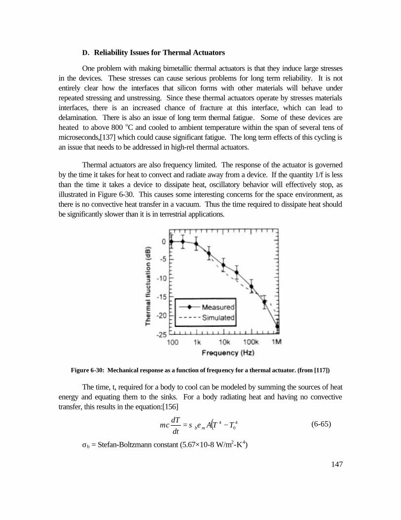
147
D. Reliability Issues for Thermal Actuators
One problem with making bimetallic thermal actuators is that they induce large stressesin the devices. These stresses can cause serious problems for long term reliability. It is notentirely clear how the interfaces that silicon forms with other materials will behave underrepeated stressing and unstressing. Since these thermal actuators operate by stresses materialsinterfaces, there is an increased chance of fracture at this interface, which can lead todelamination. There is also an issue of long term thermal fatigue. Some of these devices areheated to above 800 oC and cooled to ambient temperature within the span of several tens ofmicroseconds,[137] which could cause significant fatigue. The long term effects of this cycling isan issue that needs to be addressed in high-rel thermal actuators.
Thermal actuators are also frequency limited. The response of the actuator is governedby the time it takes for heat to convect and radiate away from a device. If the quantity 1/f is lessthan the time it takes a device to dissipate heat, oscillatory behavior will effectively stop, asillustrated in Figure 6-30. This causes some interesting concerns for the space environment, asthere is no convective heat transfer in a vacuum. Thus the time required to dissipate heat shouldbe significantly slower than it is in terrestrial applications.
Figure 6-30: Mechanical response as a function of frequency for a thermal actuator. (from [117])
The time, t, required for a body to cool can be modeled by summing the sources of heatenergy and equating them to the sinks. For a body radiating heat and having no convectivetransfer, this results in the equation:[156]
( )40
4 TTAdtdT
mc mb −= εσ
σb = Stefan-Boltzmann constant (5.67×10⁻⁸ W/m2-K4)
(6-65)
148
εm = emissivity of the material
A = the surface area of the material
T0 = initial temperature
By solving this equation, it is possible to get a limit on the time it takes for a radiativemass to cool, which indicates the frequency limit of a thermal actuator operating in the vacuumof space.
Shape memory alloys have problems unique to their structures. Since these alloys areusually made of ductile materials, they experience wear and fatigue at much faster rates thanbrittle materials. While they can withstand stress in the range of a 1 GPa, the lifetime andreliability of these devices at these stresses is unsuitable for long-term operation. If highreliability and millions of temperature cycles are desired, then nitinol should be stretched from itsmemory state only a few percent and should not exceed a couple hundred MPa of stress.
Another concern with these devices in space applications is inadvertent heating. Sincemost spacecraft experience wide temperature swings from periods of full solar exposure toeclipse, these devices will either have to have active on-chip thermal control or be in a wellthermally regulated part of the spacecraft. Otherwise there could be disastrous implications inusing thermal actuators in the space environment.
E. Additional Reading
W. Riethmüller and W Benecke, “Thermally Excited Silicon Microactuators” IEEETransactions on Electron Devices, Vol. 35, No. 6, June 1988.
P. A. Neukomm, H. P. Bornhauser, T. Hochuli, R. Paravicini, and G. Schwarz, “Characteristicsof Thin-wire Shape Memory Actuators” Transducers ’89, Proceedings of the 5th
International Conference on Solid-State Sensors and Actuators, Vol. 2, pp. 247-252, June1990.
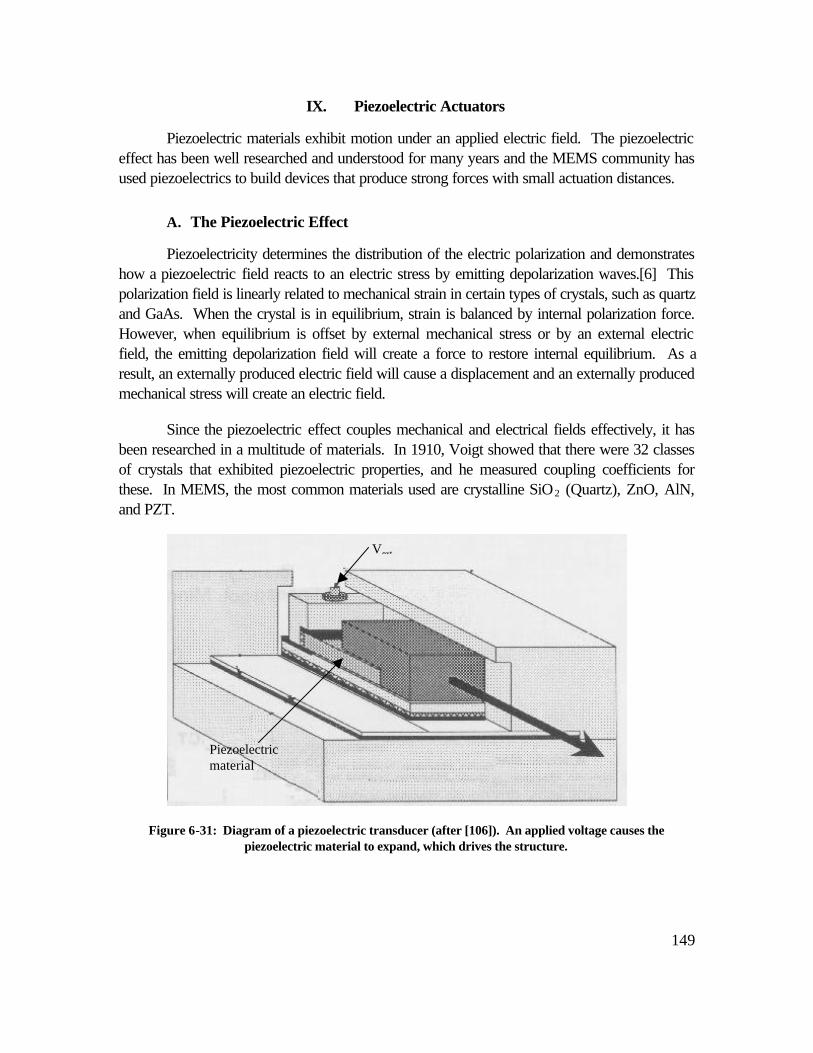
149
IX. Piezoelectric Actuators
Piezoelectric materials exhibit motion under an applied electric field. The piezoelectriceffect has been well researched and understood for many years and the MEMS community hasused piezoelectrics to build devices that produce strong forces with small actuation distances.
A. The Piezoelectric Effect
Piezoelectricity determines the distribution of the electric polarization and demonstrateshow a piezoelectric field reacts to an electric stress by emitting depolarization waves.[6] Thispolarization field is linearly related to mechanical strain in certain types of crystals, such as quartzand GaAs. When the crystal is in equilibrium, strain is balanced by internal polarization force.However, when equilibrium is offset by external mechanical stress or by an external electricfield, the emitting depolarization field will create a force to restore internal equilibrium. As aresult, an externally produced electric field will cause a displacement and an externally producedmechanical stress will create an electric field.
Since the piezoelectric effect couples mechanical and electrical fields effectively, it hasbeen researched in a multitude of materials. In 1910, Voigt showed that there were 32 classesof crystals that exhibited piezoelectric properties, and he measured coupling coefficients forthese. In MEMS, the most common materials used are crystalline SiO2 (Quartz), ZnO, AlN,and PZT.
fffVol
Vext
Piezoelectricmaterial
Figure 6-31: Diagram of a piezoelectric transducer (after [106]). An applied voltage causes thepiezoelectric material to expand, which drives the structure.
150
B. Piezoelectric Devices
Piezoelectric devices can be constructed out of a number of different structures. Acommon implementation of piezoelectrics is to produce a piezoelectric mass and connectelectrical leads to it, as shown in Figure 6-25. The extension and contraction of thepiezoelectric bar is governed by the equation:
εε eEeD +=
eEcT E += ε
where
E = the electric field
D = electric displacement at equilibrium
eε = dielectric constant at zero strain
e = is the piezoelectric stress constant
ε = mechanical strain
T =externally applied stress
cE = elastic stiffness at equilibrium
So, clearly, the mechanical displacement in this structure is coupled to the appliedelectric field. One limitation of piezoelectric devices is that the actuation distance is usuallysmall. Since piezoelectric devices operate by inducing a strain in a crystal, it would be extremelyunusual to displace a piezoelectric device more than a few percent of its total length.
Piezoelectric devices are also commonly used as sensors. Since piezoelectric materialsare electromechanically coupled, these devices can be used in much the same manner aspiezoresistive elements, with strain being converted into a change in current instead of a changein resistivity.
C. Reliability Issues
Piezoelectric devices operate by inducing stress in a material. As such, they should betreated as structural devices and be analyzed for stress distributions to prevent fracture. Thedifficulty with structural analysis in piezoelectric devices stems from the fact that piezoelectricmaterials have unusual crystal structures. Quartz, for example, is a rhombohedral structure withnine individual elastic constants. For these materials Young’s modulus and Poisson’s ratio will
(6-66a)
(6-66b)
151
exhibit less symmetry than cubic crystals. While the analyses for these materials is notintractable, it is not as straightforward as it is for cubic crystals.
Piezoelectric devices also generate a considerable heat. Since these devices aresubjected to mechanical stresses and have significant electrical losses, there is heat transferacross a device. For a rectangular piezoelectric actuator driven at a frequency f, there will be achange in temperature, ∆T, determined by:[116]
ATkufv
T e
)(=∆
where
( )( ) cmb hTTTTTk +++= 02
02)( εσ
ch = the average convective heat transfer coefficient (6-30 W/m2-K in air)
u = loss of the material per cycle
A = surface area of the piezoelectric actuator
ve = effective volume of the piezoelectric actuator (volume of the material not atequilibrium)
This heat production will stress a material and will also limit the performance of a device.Piezoelectricity is also, like piezoresistivity, temperature sensitive. As such, the heat generationmust be considered in determining the reliability characteristics of a piezoelectric device.[116]
D. Additional Reading
J. W. Judy, D. L. Polla, and W. P. Robbins, “Experimental Model and IC-Process Design of aNanometer Linear Piezoelectric Stepper Motor” Microstructures, Sensors and Actuators,DSC-Vol. 19, pp. 11-17, November, 1990.
K. Ikuta, S. Aritomi, T. Kabashima, “Tiny Silent Linear Cybernetic Actuator Driven byPiezoelectric Device with Electromagnetic Clamp”, IEEE Proceedings Microelectro-mechanical Systems, pp. 232-237, February 1992.
(6-67)
152
Chapter 7: Finite Element Analysis and Applications toMEMS
J. Newell , K. Man, and B. Stark
The design and development of MEMS is a challenging task, requiring substantialinvestment in capital equipment and plant facilities. For such investments to be fruitful, MEMSengineers must have the capability to fully characterize the inner workings of these devices, inorder to predict temperatures, stresses, dynamic response characteristics, and possible failuremechanisms. Relatively simple hand calculations can often be performed for such analyses,particularly when considering planar or beam-type geometries subject to the influence oftemperature, applied force, or pressure loads. These analyses were presented in the precedingchapter for individual devices. The finite element method provides a convenient tool forconducting more complex analyses, and will be discussed in some detail.
In finite element analysis, the structure to be analyzed is discretized into small elements,each having an associated stiffness matrix. Several finite elements have been developed torepresent common structures, including quadrilateral plates, triangular plates, solid brickelements, and beam elements. For each such element, the stiffness matrix is storedmathematically in a lookup table, in the form of fundamental equations. When problem-specificparameters such as dimensional coordinates, the material elastic modulus, Poisson’s ratio anddensity are put in these equations, the local stiffness, as represented by one element, is uniquelyknown. When a structure is fully discretized, or meshed, into many such elements, its globalstiffness can be assembled, again in the form of a matrix, from the combined stiffnesses of all theinteracting elements. If a force or set of forces is subsequently applied to the structure, the staticdisplacement response can then be calculated by inverting the global stiffness matrix, as follows:
F = kx ⇒ x = Fk-1
where F = applied force vector
k = stiffness matrix
x = displacement vector.
This basic concept can be used in the solution of many problems involving a variety ofapplied loading conditions, including externally applied static forces, pressures andtemperatures. Several example cases of such analyses are provided below.
(7-1)
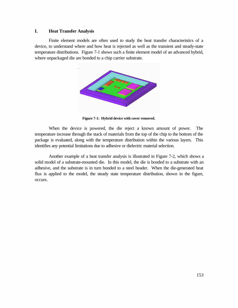
153
I. Heat Transfer Analysis
Finite element models are often used to study the heat transfer characteristics of adevice, to understand where and how heat is rejected as well as the transient and steady-statetemperature distributions. Figure 7-1 shows such a finite element model of an advanced hybrid,where unpackaged die are bonded to a chip carrier substrate.
Figure 7-1: Hybrid device with cover removed.
When the device is powered, the die reject a known amount of power. Thetemperature increase through the stack of materials from the top of the chip to the bottom of thepackage is evaluated, along with the temperature distribution within the various layers. Thisidentifies any potential limitations due to adhesive or dielectric material selection.
Another example of a heat transfer analysis is illustrated in Figure 7-2, which shows asolid model of a substrate-mounted die. In this model, the die is bonded to a substrate with anadhesive, and the substrate is in turn bonded to a steel header. When the die-generated heatflux is applied to the model, the steady state temperature distribution, shown in the figure,occurs.
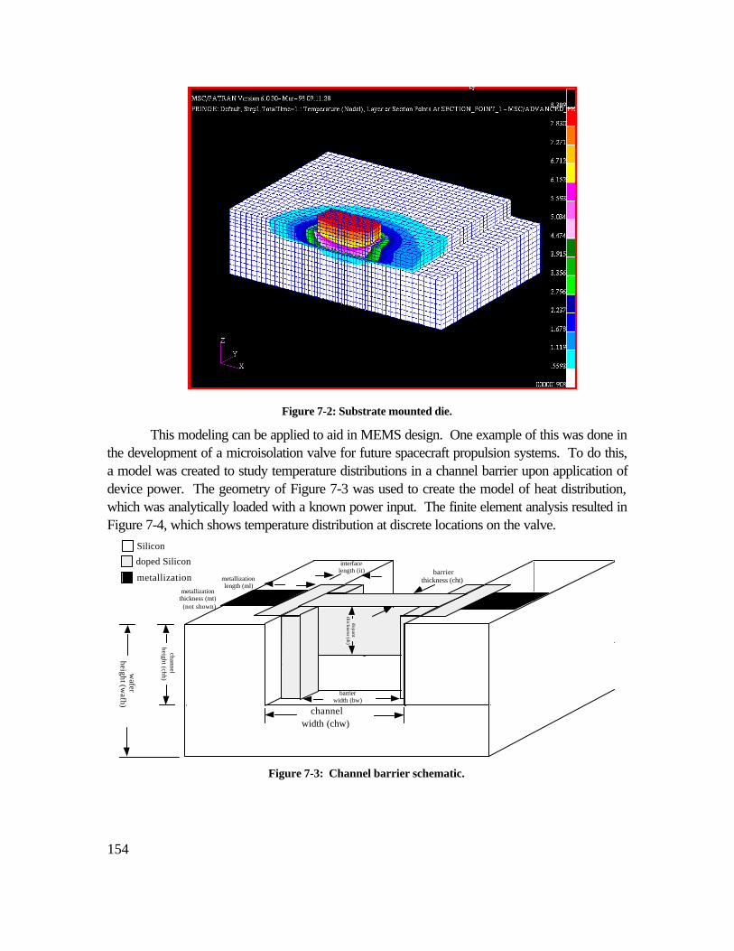
154
Figure 7-2: Substrate mounted die.
This modeling can be applied to aid in MEMS design. One example of this was done inthe development of a microisolation valve for future spacecraft propulsion systems. To do this,a model was created to study temperature distributions in a channel barrier upon application ofdevice power. The geometry of Figure 7-3 was used to create the model of heat distribution,which was analytically loaded with a known power input. The finite element analysis resulted inFigure 7-4, which shows temperature distribution at discrete locations on the valve.
doped Silicon
metallization
Silicon
channelwidth (chw)
wafer
height (wafh)
channelheight (chh)
dopantthickness (dt)
interfacelength (it)
metallizationlength (ml)
metallizationthickness (mt)
(not shown)
barrierthickness (cht)
metallizationwidth (mw)
barrierwidth (bw)
Figure 7-3: Channel barrier schematic.
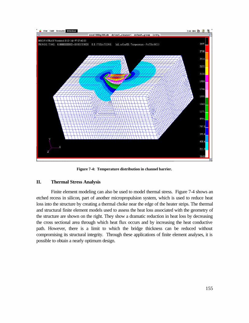
155
Figure 7-4: Temperature distribution in channel barrier.
II. Thermal Stress Analysis
Finite element modeling can also be used to model thermal stress. Figure 7-4 shows anetched recess in silicon, part of another micropropulsion system, which is used to reduce heatloss into the structure by creating a thermal choke near the edge of the heater strips. The thermaland structural finite element models used to assess the heat loss associated with the geometry ofthe structure are shown on the right. They show a dramatic reduction in heat loss by decreasingthe cross sectional area through which heat flux occurs and by increasing the heat conductivepath. However, there is a limit to which the bridge thickness can be reduced withoutcompromising its structural integrity. Through these applications of finite element analyses, it ispossible to obtain a nearly optimum design.
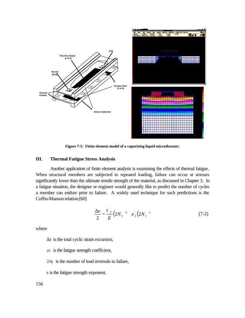
156
Inlet
Contact Pads (2 of 4)
Silicon Substrate
Thin-Film Heater (1 of 2)
Thermal Chokes
Nozzle (Exit)
Figure 7-5: Finite element model of a vaporizing liquid microthruster.
III. Thermal Fatigue Stress Analysis
Another application of finite element analysis is examining the effects of thermal fatigue.When structural members are subjected to repeated loading, failure can occur at stressessignificantly lower than the ultimate tensile strength of the material, as discussed in Chapter 3. Ina fatigue situation, the designer or engineer would generally like to predict the number of cyclesa member can endure prior to failure. A widely used technique for such predictions is theCoffin-Manson relation:[60]
( ) ( )cff
bf
f NNE
222
''
εσε
+=∆
where
∆ε is the total cyclic strain excursion,
′ σ f is the fatigue strength coefficient,
2Nf is the number of load reversals to failure,
b is the fatigue strength exponent,
(7-2)
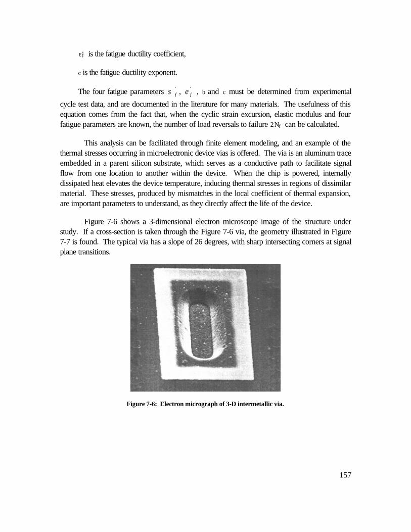
157
′ ε f is the fatigue ductility coefficient,
c is the fatigue ductility exponent.
The four fatigue parameters 'fσ , '
fε , b and c must be determined from experimental
cycle test data, and are documented in the literature for many materials. The usefulness of thisequation comes from the fact that, when the cyclic strain excursion, elastic modulus and fourfatigue parameters are known, the number of load reversals to failure 2Nf can be calculated.
This analysis can be facilitated through finite element modeling, and an example of thethermal stresses occurring in microelectronic device vias is offered. The via is an aluminum traceembedded in a parent silicon substrate, which serves as a conductive path to facilitate signalflow from one location to another within the device. When the chip is powered, internallydissipated heat elevates the device temperature, inducing thermal stresses in regions of dissimilarmaterial. These stresses, produced by mismatches in the local coefficient of thermal expansion,are important parameters to understand, as they directly affect the life of the device.
Figure 7-6 shows a 3-dimensional electron microscope image of the structure understudy. If a cross-section is taken through the Figure 7-6 via, the geometry illustrated in Figure7-7 is found. The typical via has a slope of 26 degrees, with sharp intersecting corners at signalplane transitions.
Figure 7-6: Electron micrograph of 3-D intermetallic via.
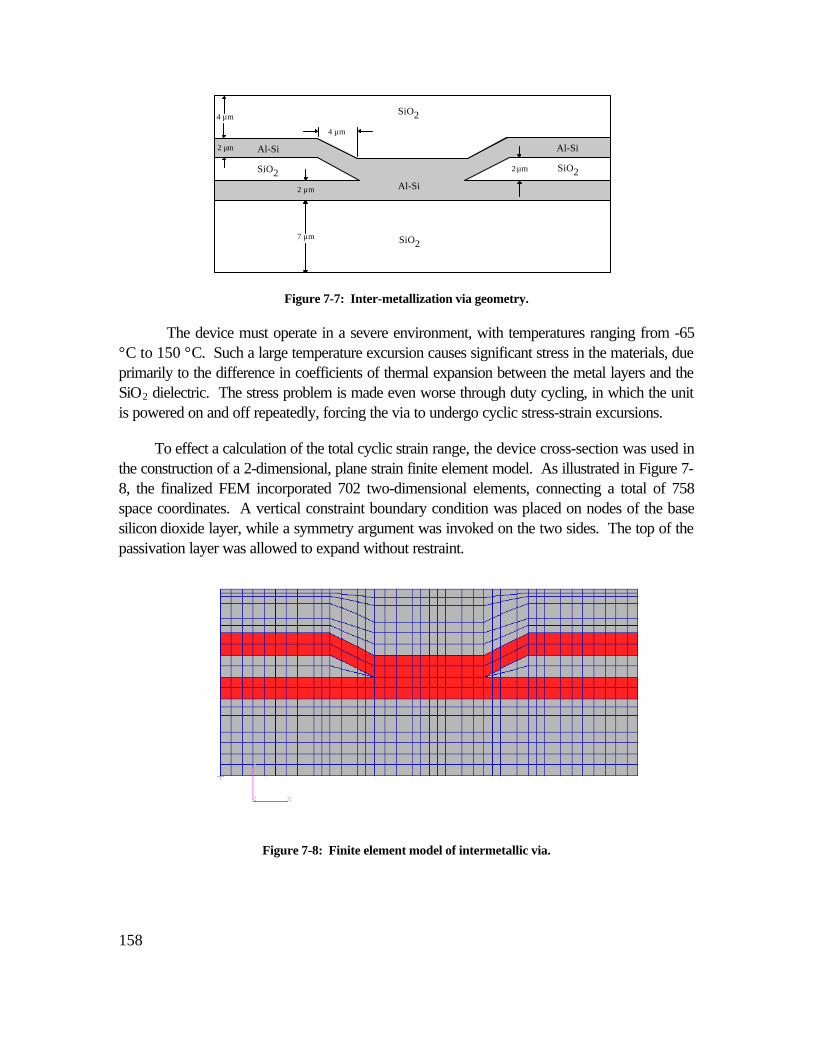
158
4 µm
2 µm
2 µm
7 µm
2µm
4 µm
Al-Si
SiO2
Al-Si
SiO2
SiO2SiO2
Al-Si
Figure 7-7: Inter-metallization via geometry.
The device must operate in a severe environment, with temperatures ranging from -65°C to 150 °C. Such a large temperature excursion causes significant stress in the materials, dueprimarily to the difference in coefficients of thermal expansion between the metal layers and theSiO2 dielectric. The stress problem is made even worse through duty cycling, in which the unitis powered on and off repeatedly, forcing the via to undergo cyclic stress-strain excursions.
To effect a calculation of the total cyclic strain range, the device cross-section was used inthe construction of a 2-dimensional, plane strain finite element model. As illustrated in Figure 7-8, the finalized FEM incorporated 702 two-dimensional elements, connecting a total of 758space coordinates. A vertical constraint boundary condition was placed on nodes of the basesilicon dioxide layer, while a symmetry argument was invoked on the two sides. The top of thepassivation layer was allowed to expand without restraint.
Figure 7-8: Finite element model of intermetallic via.
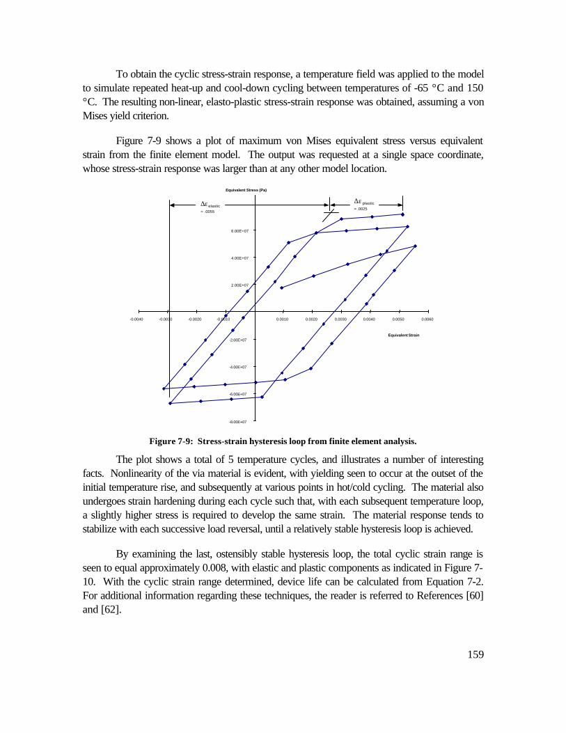
159
To obtain the cyclic stress-strain response, a temperature field was applied to the modelto simulate repeated heat-up and cool-down cycling between temperatures of -65 °C and 150°C. The resulting non-linear, elasto-plastic stress-strain response was obtained, assuming a vonMises yield criterion.
Figure 7-9 shows a plot of maximum von Mises equivalent stress versus equivalentstrain from the finite element model. The output was requested at a single space coordinate,whose stress-strain response was larger than at any other model location.
-8.00E+07
-6.00E+07
-4.00E+07
-2.00E+07
2.00E+07
4.00E+07
6.00E+07
-0.0040 -0.0030 -0.0020 -0.0010 0.0010 0.0020 0.0030 0.0040 0.0050 0.0060
Equivalent Strain
Equivalent Stress (Pa)
∆ε elastic= .0055
∆ε plastic= .0025
Figure 7-9: Stress-strain hysteresis loop from finite element analysis.
The plot shows a total of 5 temperature cycles, and illustrates a number of interestingfacts. Nonlinearity of the via material is evident, with yielding seen to occur at the outset of theinitial temperature rise, and subsequently at various points in hot/cold cycling. The material alsoundergoes strain hardening during each cycle such that, with each subsequent temperature loop,a slightly higher stress is required to develop the same strain. The material response tends tostabilize with each successive load reversal, until a relatively stable hysteresis loop is achieved.
By examining the last, ostensibly stable hysteresis loop, the total cyclic strain range isseen to equal approximately 0.008, with elastic and plastic components as indicated in Figure 7-10. With the cyclic strain range determined, device life can be calculated from Equation 7-2.For additional information regarding these techniques, the reader is referred to References [60]and [62].
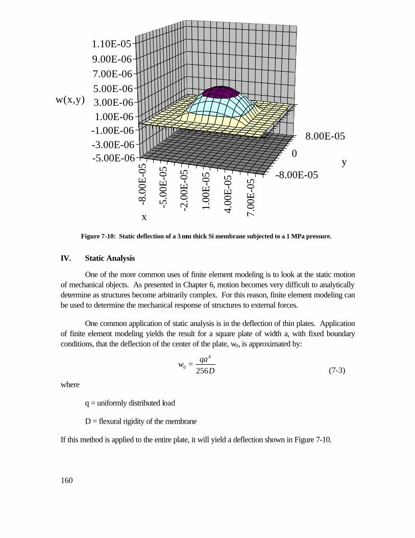
160
IV. Static Analysis
One of the more common uses of finite element modeling is to look at the static motionof mechanical objects. As presented in Chapter 6, motion becomes very difficult to analyticallydetermine as structures become arbitrarily complex. For this reason, finite element modeling canbe used to determine the mechanical response of structures to external forces.
One common application of static analysis is in the deflection of thin plates. Applicationof finite element modeling yields the result for a square plate of width a, with fixed boundaryconditions, that the deflection of the center of the plate, w0, is approximated by:
Dqa
w256
4
0 =
where
q = uniformly distributed load
D = flexural rigidity of the membrane
If this method is applied to the entire plate, it will yield a deflection shown in Figure 7-10.
(7-3)
-8.0
0E-0
5
-5.0
0E-0
5
-2.0
0E-0
5
1.00
E-05
4.00
E-05
7.00
E-05
-8.00E-05
0
8.00E-05
-5.00E-06-3.00E-06-1.00E-061.00E-063.00E-065.00E-067.00E-069.00E-061.10E-05
w(x,y)
x
y
Figure 7-10: Static deflection of a 3 µm thick Si membrane subjected to a 1 MPa pressure.
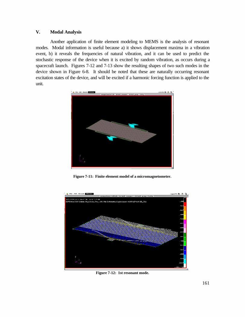
161
V. Modal Analysis
Another application of finite element modeling to MEMS is the analysis of resonantmodes. Modal information is useful because a) it shows displacement maxima in a vibrationevent, b) it reveals the frequencies of natural vibration, and it can be used to predict thestochastic response of the device when it is excited by random vibration, as occurs during aspacecraft launch. Figures 7-12 and 7-13 show the resulting shapes of two such modes in thedevice shown in Figure 6-8. It should be noted that these are naturally occurring resonantexcitation states of the device, and will be excited if a harmonic forcing function is applied to theunit.
Figure 7-11: Finite element model of a micromagnetometer.
Figure 7-12: 1st resonant mode.
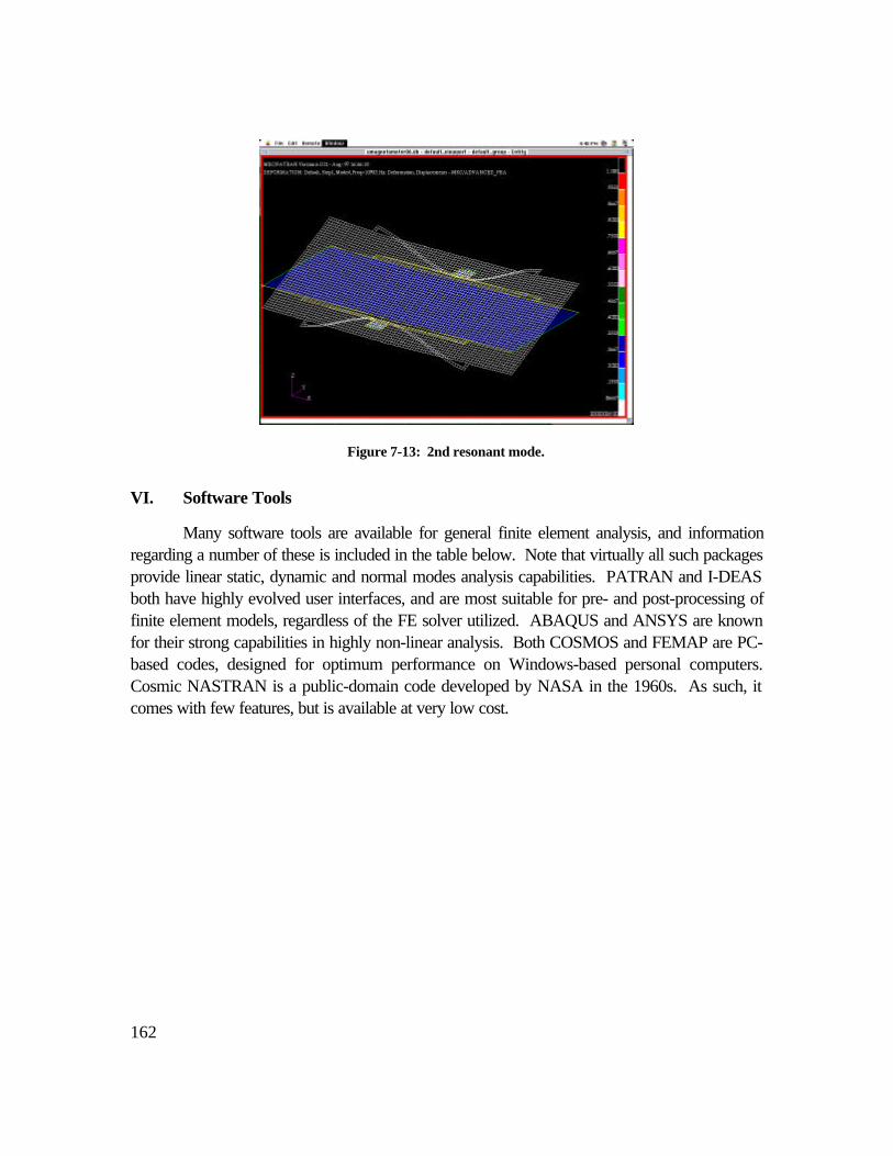
162
Figure 7-13: 2nd resonant mode.
VI. Software Tools
Many software tools are available for general finite element analysis, and informationregarding a number of these is included in the table below. Note that virtually all such packagesprovide linear static, dynamic and normal modes analysis capabilities. PATRAN and I-DEASboth have highly evolved user interfaces, and are most suitable for pre- and post-processing offinite element models, regardless of the FE solver utilized. ABAQUS and ANSYS are knownfor their strong capabilities in highly non-linear analysis. Both COSMOS and FEMAP are PC-based codes, designed for optimum performance on Windows-based personal computers.Cosmic NASTRAN is a public-domain code developed by NASA in the 1960s. As such, itcomes with few features, but is available at very low cost.
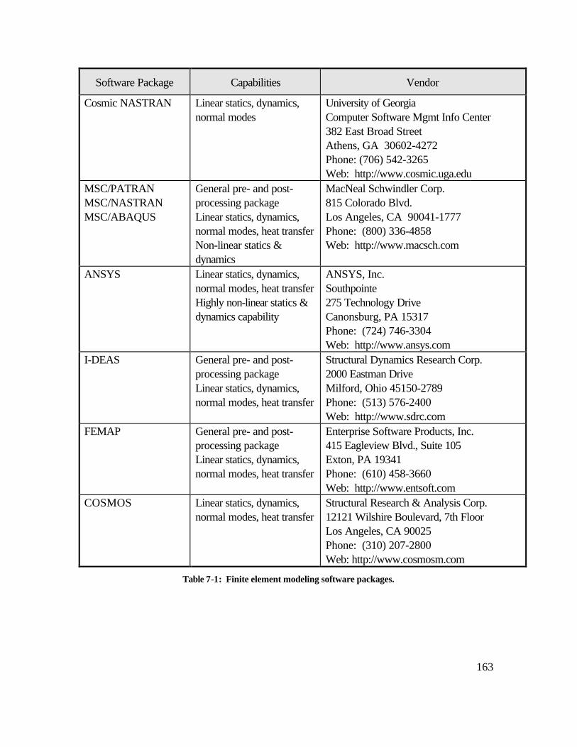
163
Software Package Capabilities Vendor
Cosmic NASTRAN Linear statics, dynamics,normal modes
University of GeorgiaComputer Software Mgmt Info Center382 East Broad StreetAthens, GA 30602-4272Phone: (706) 542-3265Web: http://www.cosmic.uga.edu
MSC/PATRANMSC/NASTRANMSC/ABAQUS
General pre- and post-processing packageLinear statics, dynamics,normal modes, heat transferNon-linear statics &dynamics
MacNeal Schwindler Corp.815 Colorado Blvd.Los Angeles, CA 90041-1777Phone: (800) 336-4858Web: http://www.macsch.com
ANSYS Linear statics, dynamics,normal modes, heat transferHighly non-linear statics &dynamics capability
ANSYS, Inc.Southpointe275 Technology DriveCanonsburg, PA 15317Phone: (724) 746-3304Web: http://www.ansys.com
I-DEAS General pre- and post-processing packageLinear statics, dynamics,normal modes, heat transfer
Structural Dynamics Research Corp.2000 Eastman DriveMilford, Ohio 45150-2789Phone: (513) 576-2400Web: http://www.sdrc.com
FEMAP General pre- and post-processing packageLinear statics, dynamics,normal modes, heat transfer
Enterprise Software Products, Inc.415 Eagleview Blvd., Suite 105Exton, PA 19341Phone: (610) 458-3660Web: http://www.entsoft.com
COSMOS Linear statics, dynamics,normal modes, heat transfer
Structural Research & Analysis Corp.12121 Wilshire Boulevard, 7th FloorLos Angeles, CA 90025Phone: (310) 207-2800Web: http://www.cosmosm.com
Table 7-1: Finite element modeling software packages.
164
VII. Additional Reading
Timoshenko, S. and Woinowsky-Krieger, Theory of Plates and Shells, 2nd edition, New York:McGraw-Hill, 1959
Roark, R. and Young, W., Roark’s Formulas for Stress and Strain, 6th edition, New York:McGraw-Hill, 1989.
Shigley, J., and Mischke, C., Mechanical Engineering Design, 5th edition, New York:McGraw-Hill, 1989.
Blevins, R., Formulas for Natural Frequency and Mode Shape, New York: Van NostrandReinhold, 1979.
Newell, J., Larson, T. and Cornford S., “A Thermo-mechanical Stress Analysis of an MCM-DInterconnect,” Proceedings of the Pan Pacific Microelectronics Symposium, Honolulu, Hawaii,February 1996.

165
166
Chapter 8: MEMS Packaging
R. D. Gerke
I. Introduction
MEMS is a relatively new field which is tied so closely with silicon processing that mostof the early packaging technologies will most likely use “off-the-shelf” packaging “borrowed”from the semiconductor microelectronics field. Packaging of microelectronics circuits is thescience and art of establishing interconnections and an appropriate operating environment forpredominantly electrical (and in the case of MEMS, electromechanical) circuits to processand/or store information.
Packaging manifests itself in novel and unique creations that ingeniously reconcile andsatisfy what seem to be mutually exclusive application requirements and constraints posed by thelaws of nature and the properties of materials and processes. All applications can be summedup in three terms: cost, performance and reliability.
Packaging can span from the consumer to midrange systems to the highperformance/reliability applications. It must be noted that no sharp boundaries exist betweenthe classes, only a gradual shift from optimization for parameters which control performance andcause the cost to increase. All along, the reliability must also be considered. The packagingchapter that follows will summarize the primary package types that will likely apply to MEMStechnology and the concerns that traditionally have concerned the microelectronics field.
Webster’s dictionary defines package as a group or a number of things, boxed andoffered as a unit. MEMS packages can contain many electrical and mechanical components.To be useful to the outside world these components need interconnections. Alone, a MEM diesawed from a wafer is extremely fragile and must be protected from mechanical damage andhostile environments. To function, electrical circuits need to be supplied with electrical energy,which is consumed and transformed into mechanical and thermal (heat) energy. Because thesystem operates best within a limited temperature range, packaging must offer an adequatemeans for removal of heat.
II. Functions of MEMS Packages
The package serves to integrate all of the components required for a system applicationin a manner that minimizes size, cost, mass and complexity. The package provides the interfacebetween the components and the overall system. The following subsections present the threemain functions of the MEMS package: mechanical support, protection from the environment,and electrical connection to other system components.
167
A. Mechanical Support
Due to the very nature of MEMS being mechanical, the requirement to support andprotect the device from thermal and mechanical shock, vibration, high acceleration, particles,and other physical damage (possibly radiation) during storage and operation of the partbecomes critical. The mechanical stress endured depends on the mission or application. Forexample, landing a spacecraft on a planet's surface creates greater mechanical shock thanexperienced by a communication satellite. There is also a difference between space andterrestrial applications.
The coefficient of thermal expansion (CTE) of the package should be equal to or slightlygreater than the CTE of silicon for reliability, since thermal shock or thermal cycling may causedie cracking and delamination if the materials are unmatched or if the silicon is subject to tensilestress. Other important parameters are thermal resistance of the carrier, the material's electricalproperties, and its chemical properties, or resistance to corrosion.
Once the MEMS device is supported on a (chip) carrier, the wire bonds or otherelectrical connections are made, the assembly must be protected from scratches, particulates,and other physical damage. This is accomplished either by adding walls and a cover to the baseor by encapsulating the assembly in plastic or other material. Since the electrical connections tothe package are usually made through the walls, the walls are typically made from glass orceramic. The glass or ceramic can also be used to provide electrical insulation of the leads asthey exit through a conducting package wall (metal or composite materials). Although the CTEof the package walls and lid do not have to match the CTE of silicon based MEMS as they arenot in intimate contact (unless an encapsulating material is used), it should match the CTE of thecarrier or base to which they are connected.
B. Protection From Environment
a) The Simple – Mechanical only
Many MEMS devices are designed to measure something in the immediate surroundingenvironment. These devices range from biological ‘sniffers’ to chemical MEMS that measureconcentrations of certain types of liquids. So the traditional ‘hermeticity’ that is generallythought of for protecting microelectronic devices may not apply to all MEMS devices. Thesedevices might be directly mounted to a printed circuit board (PCB) or a hybrid–like ceramicsubstrate and have nothing but a ‘housing’ to protect it from mechanical damage such asdropping or something as simple as damage from the operator’s thumb.
b) The Traditional – Hermetic and non-Hermetic
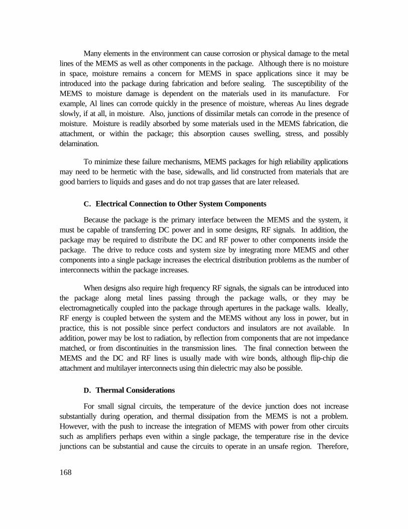
168
Many elements in the environment can cause corrosion or physical damage to the metallines of the MEMS as well as other components in the package. Although there is no moisturein space, moisture remains a concern for MEMS in space applications since it may beintroduced into the package during fabrication and before sealing. The susceptibility of theMEMS to moisture damage is dependent on the materials used in its manufacture. Forexample, Al lines can corrode quickly in the presence of moisture, whereas Au lines degradeslowly, if at all, in moisture. Also, junctions of dissimilar metals can corrode in the presence ofmoisture. Moisture is readily absorbed by some materials used in the MEMS fabrication, dieattachment, or within the package; this absorption causes swelling, stress, and possiblydelamination.
To minimize these failure mechanisms, MEMS packages for high reliability applicationsmay need to be hermetic with the base, sidewalls, and lid constructed from materials that aregood barriers to liquids and gases and do not trap gasses that are later released.
C. Electrical Connection to Other System Components
Because the package is the primary interface between the MEMS and the system, itmust be capable of transferring DC power and in some designs, RF signals. In addition, thepackage may be required to distribute the DC and RF power to other components inside thepackage. The drive to reduce costs and system size by integrating more MEMS and othercomponents into a single package increases the electrical distribution problems as the number ofinterconnects within the package increases.
When designs also require high frequency RF signals, the signals can be introduced intothe package along metal lines passing through the package walls, or they may beelectromagnetically coupled into the package through apertures in the package walls. Ideally,RF energy is coupled between the system and the MEMS without any loss in power, but inpractice, this is not possible since perfect conductors and insulators are not available. Inaddition, power may be lost to radiation, by reflection from components that are not impedancematched, or from discontinuities in the transmission lines. The final connection between theMEMS and the DC and RF lines is usually made with wire bonds, although flip-chip dieattachment and multilayer interconnects using thin dielectric may also be possible.
D. Thermal Considerations
For small signal circuits, the temperature of the device junction does not increasesubstantially during operation, and thermal dissipation from the MEMS is not a problem.However, with the push to increase the integration of MEMS with power from other circuitssuch as amplifiers perhaps even within a single package, the temperature rise in the devicejunctions can be substantial and cause the circuits to operate in an unsafe region. Therefore,
169
thermal dissipation requirements for power amplifiers, other large signal circuits, and highlyintegrated packages can place severe design constraints on the package design.
The junction temperature of an isolated device can be determined by
Tj = Q * R, + Tcase
where
Q is the heat generated by the junction and is dependent on the output power of thedevice and its efficiency,
R is the thermal resistance between the junction and the case, and
T is the temperature of the case.
Normally, the package designer has no control over Q and the case temperature, andtherefore, it is the thermal resistance of the package that must be minimized. Figure 8-1 is aschematic representation of the thermal circuit for a typical package, where it is assumed that thepackage base is in contact with a heat sink or case.
It is seen that there are three thermal resistances that must be minimized: the resistancethrough the package substrate, the resistance through the die-attach material, and the resistancethrough the carrier or package base. Furthermore, the thermal resistance of each is dependenton the thermal resistivity and the thickness of the material. A package base made of metal ormetal composites has very low thermal resistance and therefore does not add substantially to thetotal resistance. When electrically insulating materials are used for bases metal-filled via holesare routinely used, under the MEMS, to provide a thermal path to the heat sink. Althoughthermal resistance is a consideration in the choice of the die attach material, adhesion and bondstrength are even more important. To minimize the thermal resistance through the die-attachmaterial, the material must be thin, there can be no voids, and the two surfaces to be bondedshould be smooth.
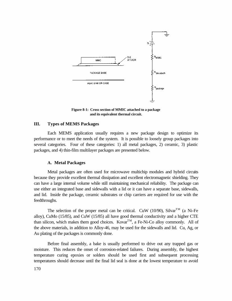
170
Figure 8-1: Cross section of MMIC attached to a packageand its equivalent thermal circuit.
III. Types of MEMS Packages
Each MEMS application usually requires a new package design to optimize itsperformance or to meet the needs of the system. It is possible to loosely group packages intoseveral categories. Four of these categories: 1) all metal packages, 2) ceramic, 3) plasticpackages, and 4) thin-film multilayer packages are presented below.
A. Metal Packages
Metal packages are often used for microwave multichip modules and hybrid circuitsbecause they provide excellent thermal dissipation and excellent electromagnetic shielding. Theycan have a large internal volume while still maintaining mechanical reliability. The package canuse either an integrated base and sidewalls with a lid or it can have a separate base, sidewalls,and lid. Inside the package, ceramic substrates or chip carriers are required for use with thefeedthroughs.
The selection of the proper metal can be critical. CuW (10/90), SilvarTM (a Ni-Fealloy), CuMo (15/85), and CuW (15/85) all have good thermal conductivity and a higher CTEthan silicon, which makes them good choices. KovarTM, a Fe-Ni-Co alloy commonly. All ofthe above materials, in addition to Alloy-46, may be used for the sidewalls and lid. Cu, Ag, orAu plating of the packages is commonly done.
Before final assembly, a bake is usually performed to drive out any trapped gas ormoisture. This reduces the onset of corrosion-related failures. During assembly, the highesttemperature curing epoxies or solders should be used first and subsequent processingtemperatures should decrease until the final lid seal is done at the lowest temperature to avoid
171
later steps damaging earlier steps. Au-Sn is a commonly used solder that works well when thetwo materials to be bonded have similar CTEs. Au-Sn solder joints of materials with a largeCTE mismatch are susceptible to fatigue failures after temperature cycling. The AuSnintermetallics that form tend to be brittle and can accommodate only low amounts of stress.
Welding (using lasers to locally heat the joint between the two parts without raising thetemperature of the entire part) is a commonly used alternative to solders. Regardless of the sealtechnology, no voids or misalignments can be tolerated since they can compromise the packagehermeticity. Hermeticity can also be affected by the feedthroughs that are required in metalpackages. These feedthroughs are generally made of glass or ceramic and each method (glassseal or aluminum feedthrough) has its weakness. Glass can crack during handling and thermalcycling. The conductor exiting through the ceramic feedthrough may not seal properly due tometallurgical reasons. Generally, these failures are due to processing problems as the ceramicmust be metallized so that the conductor (generally metal) may be soldered (or brazed) to it.The metallization process must allow for complete wetting of the conducting pin to the ceramic.Incomplete wetting can show up as a failure during thermal cycle testing.
B. Ceramic Packages
Ceramic packages have several features that make them especially useful formicroelectronics as well as MEMS. They provide low mass, are easily mass produced, and canbe low in cost. They can be made hermetic, and can more easily integrate signal distribution linesand feedthroughs. They can be machined to perform many different functions. By incorporatingmultiple layers of ceramics and interconnect lines, electrical performance of the package can betailored to meet design requirements. These types of packages are generally referred to as co-fired multilayer ceramic packages. Details of the co-fired process are outlined below.Multilayer ceramic packages also allow reduced size and cost of the total system by integratingmultiple MEMS and/or other components into a single, hermetic package. These multilayerpackages offer significant size and mass reduction over metal-walled packages. Most of thatadvantage is derived by the use of three dimensions instead of two for interconnect lines.
Co-fired ceramic packages are constructed from individual pieces of ceramic in the"green" or unfired state. These materials are thin, pliable films. During a typical process, thefilms are stretched across a frame in a way similar to that used by an artist to stretch a canvasacross a frame. On each layer, metal lines are deposited using thick-film processing (usuallyscreen printing), and via holes for interlayer interconnects are drilled or punched. After all of thelayers have been fabricated, the unfired pieces are stacked and aligned using registration holesand laminated together. Finally, the part is fired at a high temperature. The MEMS andpossibly other components are then attached into place (usually organically (epoxy) ormetallurgically (solders), and wire bonds are made the same as those used for metal packages.
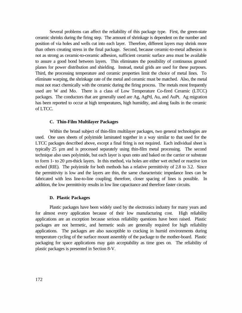
172
Several problems can affect the reliability of this package type. First, the green-stateceramic shrinks during the firing step. The amount of shrinkage is dependent on the number andposition of via holes and wells cut into each layer. Therefore, different layers may shrink morethan others creating stress in the final package. Second, because ceramic-to-metal adhesion isnot as strong as ceramic-to-ceramic adhesion, sufficient ceramic surface area must be availableto assure a good bond between layers. This eliminates the possibility of continuous groundplanes for power distribution and shielding. Instead, metal grids are used for these purposes.Third, the processing temperature and ceramic properties limit the choice of metal lines. Toeliminate warping, the shrinkage rate of the metal and ceramic must be matched. Also, the metalmust not react chemically with the ceramic during the firing process. The metals most frequentlyused are W and Mo. There is a class of Low Temperature Co-fired Ceramic (LTCC)packages. The conductors that are generally used are Ag, AgPd, Au, and AuPt. Ag migrationhas been reported to occur at high temperatures, high humidity, and along faults in the ceramicof LTCC.
C. Thin-Film Multilayer Packages
Within the broad subject of thin-film multilayer packages, two general technologies areused. One uses sheets of polyimide laminated together in a way similar to that used for theLTCC packages described above, except a final firing is not required. Each individual sheet istypically 25 µm and is processed separately using thin-film metal processing. The secondtechnique also uses polyimide, but each layer is spun onto and baked on the carrier or substrateto form 1- to 20 µm-thick layers. In this method, via holes are either wet etched or reactive ionetched (RIE). The polyimide for both methods has a relative permittivity of 2.8 to 3.2. Sincethe permittivity is low and the layers are thin, the same characteristic impedance lines can befabricated with less line-to-line coupling; therefore, closer spacing of lines is possible. Inaddition, the low permittivity results in low line capacitance and therefore faster circuits.
D. Plastic Packages
Plastic packages have been widely used by the electronics industry for many years andfor almost every application because of their low manufacturing cost. High reliabilityapplications are an exception because serious reliability questions have been raised. Plasticpackages are not hermetic, and hermetic seals are generally required for high reliabilityapplications. The packages are also susceptible to cracking in humid environments duringtemperature cycling of the surface mount assembly of the package to the mother-board. Plasticpackaging for space applications may gain acceptability as time goes on. The reliability ofplastic packages is presented in Section 8-V.
173
IV. Package-to-MEMS Attachment
The method used to attach a MEMS device to a package is a general technology applicable tomost Integrated Circuit (IC) devices. Generally referred to as die attach, the function servesseveral critical functions. The main function is to provide good mechanical attachment of theMEMS structure to the package base. This ensures that the MEMS chip (or die) does notmove relative to the package base. It must survive hot and cold temperatures, moisture, shockand vibration. The attachment may also be required to provide a good thermal path betweenthe MEMS structure and the package base. Should heat be generated by the MEMS structureor by the support circuitry, the attachment material should be able to conduct the heat from thechip to the package base. The heat can be conducted away from the chip and ‘spread’ to thepackage base which is larger in size and has more thermal mass. This spreading can keep thedevice operating in the desired temperature range. If the support circuitry requires goodelectrical contact from the silicon to the package base, the attachment material should be able toaccommodate the task.
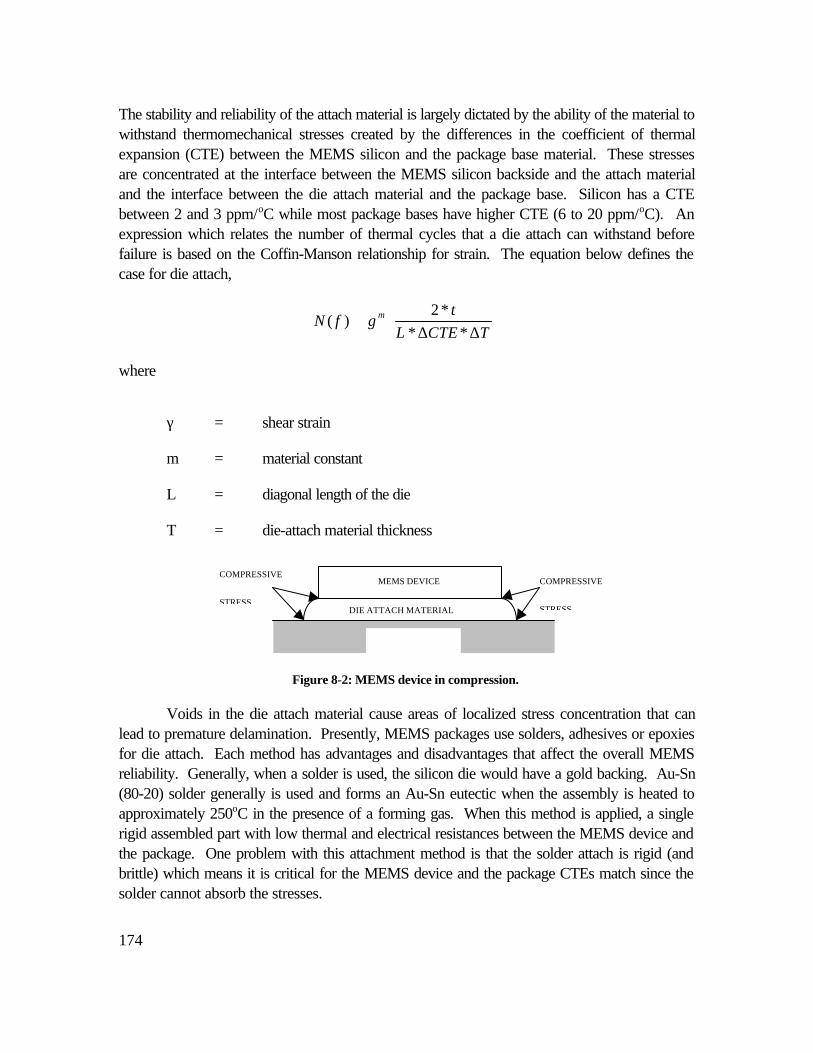
174
The stability and reliability of the attach material is largely dictated by the ability of the material towithstand thermomechanical stresses created by the differences in the coefficient of thermalexpansion (CTE) between the MEMS silicon and the package base material. These stressesare concentrated at the interface between the MEMS silicon backside and the attach materialand the interface between the die attach material and the package base. Silicon has a CTEbetween 2 and 3 ppm/oC while most package bases have higher CTE (6 to 20 ppm/oC). Anexpression which relates the number of thermal cycles that a die attach can withstand beforefailure is based on the Coffin-Manson relationship for strain. The equation below defines thecase for die attach,
∆∆∝
TCTELt
fN m
***2
)( γ
where
γ = shear strain
m = material constant
L = diagonal length of the die
T = die-attach material thickness
Figure 8-2: MEMS device in compression.
Voids in the die attach material cause areas of localized stress concentration that canlead to premature delamination. Presently, MEMS packages use solders, adhesives or epoxiesfor die attach. Each method has advantages and disadvantages that affect the overall MEMSreliability. Generally, when a solder is used, the silicon die would have a gold backing. Au-Sn(80-20) solder generally is used and forms an Au-Sn eutectic when the assembly is heated toapproximately 250oC in the presence of a forming gas. When this method is applied, a singlerigid assembled part with low thermal and electrical resistances between the MEMS device andthe package. One problem with this attachment method is that the solder attach is rigid (andbrittle) which means it is critical for the MEMS device and the package CTEs match since thesolder cannot absorb the stresses.
COMPRESSIVE
STRESS
COMPRESSIVE
STRESSDIE ATTACH MATERIAL
MEMS DEVICE
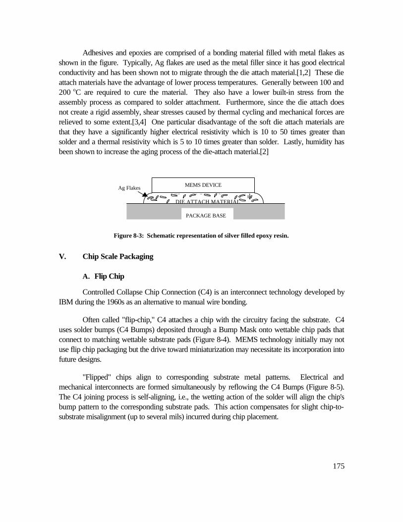
175
Adhesives and epoxies are comprised of a bonding material filled with metal flakes asshown in the figure. Typically, Ag flakes are used as the metal filler since it has good electricalconductivity and has been shown not to migrate through the die attach material.[1,2] These dieattach materials have the advantage of lower process temperatures. Generally between 100 and200 oC are required to cure the material. They also have a lower built-in stress from theassembly process as compared to solder attachment. Furthermore, since the die attach doesnot create a rigid assembly, shear stresses caused by thermal cycling and mechanical forces arerelieved to some extent.[3,4] One particular disadvantage of the soft die attach materials arethat they have a significantly higher electrical resistivity which is 10 to 50 times greater thansolder and a thermal resistivity which is 5 to 10 times greater than solder. Lastly, humidity hasbeen shown to increase the aging process of the die-attach material.[2]
Figure 8-3: Bonding material.
Figure 8-3: Schematic representation of silver filled epoxy resin.
V. Chip Scale Packaging
A. Flip Chip
Controlled Collapse Chip Connection (C4) is an interconnect technology developed byIBM during the 1960s as an alternative to manual wire bonding.
Often called "flip-chip," C4 attaches a chip with the circuitry facing the substrate. C4uses solder bumps (C4 Bumps) deposited through a Bump Mask onto wettable chip pads thatconnect to matching wettable substrate pads (Figure 8-4). MEMS technology initially may notuse flip chip packaging but the drive toward miniaturization may necessitate its incorporation intofuture designs.
"Flipped" chips align to corresponding substrate metal patterns. Electrical andmechanical interconnects are formed simultaneously by reflowing the C4 Bumps (Figure 8-5).The C4 joining process is self-aligning, i.e., the wetting action of the solder will align the chip'sbump pattern to the corresponding substrate pads. This action compensates for slight chip-to-substrate misalignment (up to several mils) incurred during chip placement.
DIE ATTACH MATERIAL
MEMS DEVICE
PACKAGE BASE
Ag Flakes
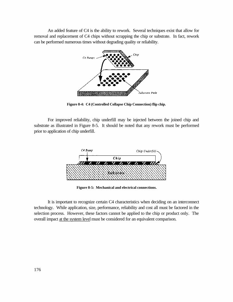
176
An added feature of C4 is the ability to rework. Several techniques exist that allow forremoval and replacement of C4 chips without scrapping the chip or substrate. In fact, reworkcan be performed numerous times without degrading quality or reliability.
Figure 8-4: C4 (Controlled Collapse Chip Connection) flip chip.
For improved reliability, chip underfill may be injected between the joined chip andsubstrate as illustrated in Figure 8-5. It should be noted that any rework must be performedprior to application of chip underfill.
Figure 8-5: Mechanical and electrical connections.
It is important to recognize certain C4 characteristics when deciding on an interconnecttechnology. While application, size, performance, reliability and cost all must be factored in theselection process. However, these factors cannot be applied to the chip or product only. Theoverall impact at the system level must be considered for an equivalent comparison.
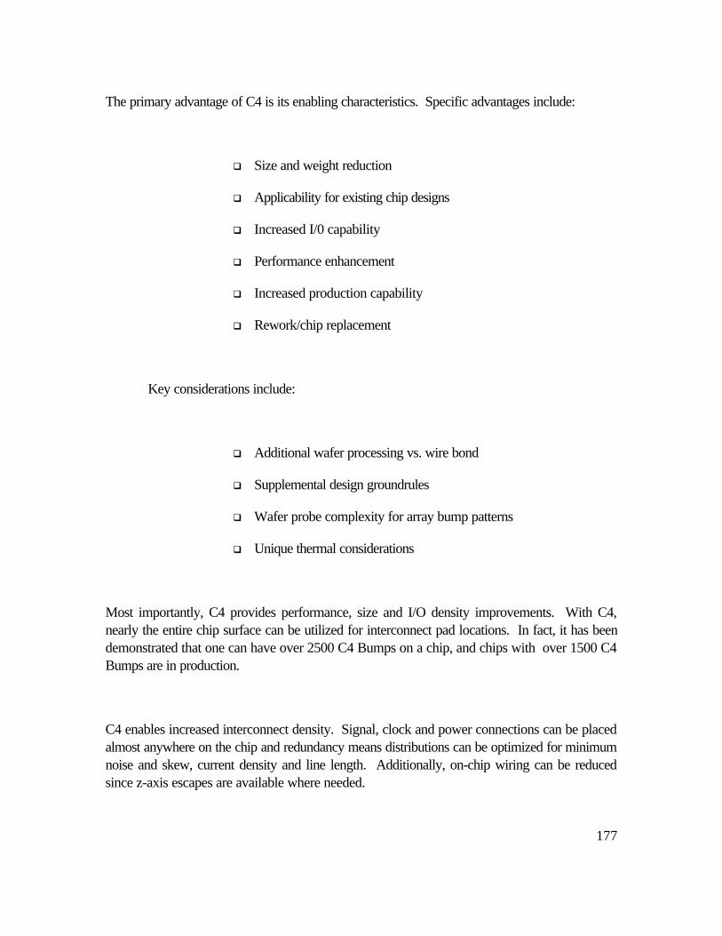
177
The primary advantage of C4 is its enabling characteristics. Specific advantages include:
q Size and weight reduction
q Applicability for existing chip designs
q Increased I/0 capability
q Performance enhancement
q Increased production capability
q Rework/chip replacement
Key considerations include:
q Additional wafer processing vs. wire bond
q Supplemental design groundrules
q Wafer probe complexity for array bump patterns
q Unique thermal considerations
Most importantly, C4 provides performance, size and I/O density improvements. With C4,nearly the entire chip surface can be utilized for interconnect pad locations. In fact, it has beendemonstrated that one can have over 2500 C4 Bumps on a chip, and chips with over 1500 C4Bumps are in production.
C4 enables increased interconnect density. Signal, clock and power connections can be placedalmost anywhere on the chip and redundancy means distributions can be optimized for minimumnoise and skew, current density and line length. Additionally, on-chip wiring can be reducedsince z-axis escapes are available where needed.
178
Figure 8-6 compares single row wirebond and C4 chips. Each chip is 8 mm (200 mil) square.Wirebond pitch is 76 µm (3 mil) pads on 100 µm (4 mil) centers. C4 pitch is 100 µm (4 mil)bumps on 230 µm (9 mil) centers. In this example, interconnect density is increased over 140%using C4.
Figure 8-6: Interconnect density (wire bond vs. C4).
The reliability of flip-chip contacts is determined by the difference in the CTE betweenthe chip and the ceramic substrate or the organic printed circuit board (PCB). For example, theCTE for silicon is ~2 – 3 ppm/oK, for 96% alumina it is 6.4 ppm/oK, and for PCB it is typically20 to 25 ppm/oK. The CTE mismatch between the chip and the carrier induces high thermaland mechanical stresses and strain at the contact bumps. The highest strain occurs at the cornerjoints, whose distance is the largest from the distance neutral point (DNP) on the chip. Forexample, the DNP for a 2.5- x 2.5-mm chip is 1.7 mm. The thermomechanical stress and straincause the joints to crack. When these cracks become large, the contact resistance increases,and the flow of current is inhibited. This ultimately leads to chip electrical failure. The typicalreliability defined failure criterion is an increase in resistance in excess of 30 mΩ over the zerotime value.[5] The tradeoff in selecting the bump height is that large bumps introduce a seriesinductance that degrades high-frequency performance and increases the thermal resistance fromthe device to the carrier, if that is the primary heat path.
The reliability of the bump joints is improved if, after reflow, a bead of encapsulatingepoxy resin is dispensed near the chip and drawn by capillary action into the space between thechip and the carrier. The epoxy is then cured to provide the final flip-chip assembly. Figure 8-5

179
shows a typical flip-chip package. The epoxy-resin underfill mechanically couples the chip andthe carrier and locally constrains the CTE mismatch, thus improving the reliability of the joints.The most essential characteristic of the encapsulant is a good CTE match with the z-expansionof the solder or the bump material. For example, if one uses 95 Pb/5 Sn solder having a CTEof 28 ppm/oK, an encapsulant with a CTE of about 25 ppm/oK is recommended. Underfillingalso allows packaging of larger chips by increasing the allowable DNP. In some cases, theencapsulant acts as a protective layer on the active surface of the chip
Good adhesion among the underfill material, the carrier, and the chip surface is neededfor stress compensation. The adhesion between the surfaces can be lost and delamination cantake place if contaminants, such as post-reflow flux residue, are present. For this reason, afluxless process for flip-chip assembly is desirable.[5] Unfortunately, flip-chip bonding on PCBrequires the use of flux.[6] However, on ceramic carriers with gold, silver, and palladium-silverthick-film patterns and via metallizations, fluxless flipchip thermocompression bonding with gold-tin bumps has demonstrated high reliability.[5] The results of reliability testing[5] are summarizedin Table 8-1 and may serve as a guideline for future work.
Parameter Value
Bump height 30 to 70 µmChip size A few mmChip carrier CeramicCarrier camber 5 µm per cmCamber compensation By bump deformationUnderfill YesThermal cycling After 6500 cycles (-55oC to +125oC), no contact failure and no
change in contact resistanceHigh-temperature storage After 1000 h, no increase in contact resistanceTemperature and humidity After 1000 h (85'C and 85% RH), no change in contact
resistancePressure-cooker test After 1000 h (121oC and 29.7 psi), contact resistance increased
slightly from 3 mW to 4 mW
Table 8-1: Summary of reliability test conditions and results for fluxless flip-chip thermocompression-bonded bump contacts.
Finally, care should be taken that the encapsulant or underfill covers the entire undersidewithout air pockets or voids, and forms complete edge fillets around all four sides of the chip.Voids create high-stress concentrations and may lead to early delamination of the encapsulant.After assembly, a scanning acoustic microscope can be used to locate voids in the encapsulant.The encapsulant should also be checked for microcracks or surface flaws, which have a
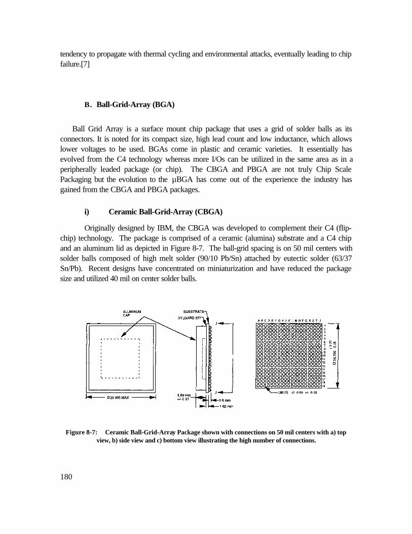
180
tendency to propagate with thermal cycling and environmental attacks, eventually leading to chipfailure.[7]
B. Ball-Grid-Array (BGA)
Ball Grid Array is a surface mount chip package that uses a grid of solder balls as itsconnectors. It is noted for its compact size, high lead count and low inductance, which allowslower voltages to be used. BGAs come in plastic and ceramic varieties. It essentially hasevolved from the C4 technology whereas more I/Os can be utilized in the same area as in aperipherally leaded package (or chip). The CBGA and PBGA are not truly Chip ScalePackaging but the evolution to the µBGA has come out of the experience the industry hasgained from the CBGA and PBGA packages.
i) Ceramic Ball-Grid-Array (CBGA)
Originally designed by IBM, the CBGA was developed to complement their C4 (flip-chip) technology. The package is comprised of a ceramic (alumina) substrate and a C4 chipand an aluminum lid as depicted in Figure 8-7. The ball-grid spacing is on 50 mil centers withsolder balls composed of high melt solder (90/10 Pb/Sn) attached by eutectic solder (63/37Sn/Pb). Recent designs have concentrated on miniaturization and have reduced the packagesize and utilized 40 mil on center solder balls.
Figure 8-7: Ceramic Ball-Grid-Array Package shown with connections on 50 mil centers with a) topview, b) side view and c) bottom view illustrating the high number of connections.
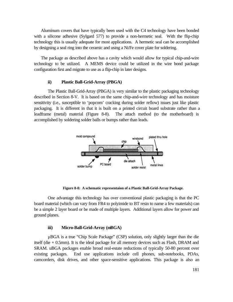
181
Aluminum covers that have typically been used with the C4 technology have been bondedwith a silicone adhesive (Sylgard 577) to provide a non-hermetic seal. With the flip-chiptechnology this is usually adequate for most applications. A hermetic seal can be accomplishedby designing a seal ring into the ceramic and using a Ni/Fe cover plate for soldering.
The package as described above has a cavity which would allow for typical chip-and-wiretechnology to be utilized. A MEMS device could be utilized in the wire bond packageconfiguration first and migrate to use as a flip-chip in later designs.
ii) Plastic Ball-Grid-Array (PBGA)
The Plastic Ball-Grid-Array (PBGA) is very similar to the plastic packaging technologydescribed in Section 8-V. It is based on the same chip-and-wire technology and has moisturesensitivity (i.e., susceptible to ‘popcorn’ cracking during solder reflow) issues just like plasticpackaging. It is different in that it is built on a printed circuit board substrate rather than aleadframe (metal) material (Figure 8-8). The attach method (to the motherboard) isaccomplished by soldering solder balls or bumps rather than leads.
Figure 8-8: A schematic representaion of a Plastic Ball-Grid-Array Package.
One advantage this technology has over conventional plastic packaging is that the PCboard material (which can vary from FR4 to polyimide to BT resin to name a few materials) canbe a simple 2 layer board or be made of multiple layers. Additional layers allow for power andground planes.
iii) Micro-Ball-Grid-Array (µBGA)
µBGA is a true “Chip Scale Package” (CSP) solution, only slightly larger than the dieitself (die + 0.5mm). It is the ideal package for all memory devices such as Flash, DRAM andSRAM. uBGA packages enable broad real-estate reductions of typically 50-80 percent overexisting packages. End use applications include cell phones, sub-notebooks, PDAs,camcorders, disk drives, and other space-sensitive applications. This package is also an
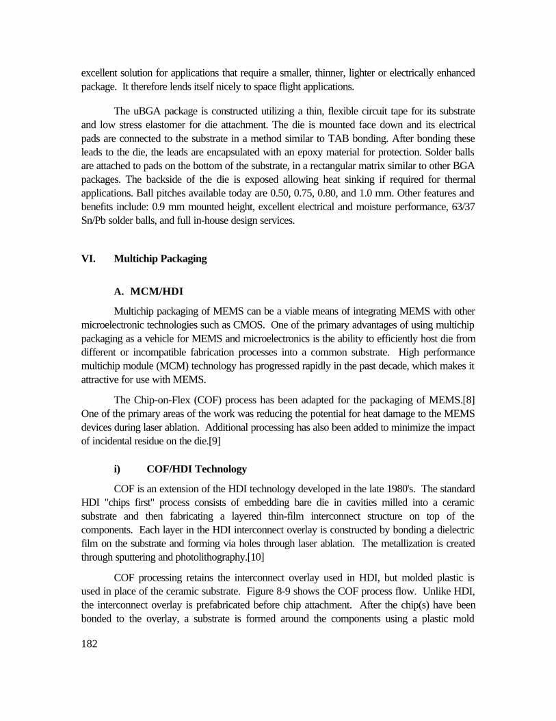
182
excellent solution for applications that require a smaller, thinner, lighter or electrically enhancedpackage. It therefore lends itself nicely to space flight applications.
The uBGA package is constructed utilizing a thin, flexible circuit tape for its substrateand low stress elastomer for die attachment. The die is mounted face down and its electricalpads are connected to the substrate in a method similar to TAB bonding. After bonding theseleads to the die, the leads are encapsulated with an epoxy material for protection. Solder ballsare attached to pads on the bottom of the substrate, in a rectangular matrix similar to other BGApackages. The backside of the die is exposed allowing heat sinking if required for thermalapplications. Ball pitches available today are 0.50, 0.75, 0.80, and 1.0 mm. Other features andbenefits include: 0.9 mm mounted height, excellent electrical and moisture performance, 63/37Sn/Pb solder balls, and full in-house design services.
VI. Multichip Packaging
A. MCM/HDI
Multichip packaging of MEMS can be a viable means of integrating MEMS with othermicroelectronic technologies such as CMOS. One of the primary advantages of using multichippackaging as a vehicle for MEMS and microelectronics is the ability to efficiently host die fromdifferent or incompatible fabrication processes into a common substrate. High performancemultichip module (MCM) technology has progressed rapidly in the past decade, which makes itattractive for use with MEMS.
The Chip-on-Flex (COF) process has been adapted for the packaging of MEMS.[8]One of the primary areas of the work was reducing the potential for heat damage to the MEMSdevices during laser ablation. Additional processing has also been added to minimize the impactof incidental residue on the die.[9]
i) COF/HDI Technology
COF is an extension of the HDI technology developed in the late 1980's. The standardHDI "chips first" process consists of embedding bare die in cavities milled into a ceramicsubstrate and then fabricating a layered thin-film interconnect structure on top of thecomponents. Each layer in the HDI interconnect overlay is constructed by bonding a dielectricfilm on the substrate and forming via holes through laser ablation. The metallization is createdthrough sputtering and photolithography.[10]
COF processing retains the interconnect overlay used in HDI, but molded plastic isused in place of the ceramic substrate. Figure 8-9 shows the COF process flow. Unlike HDI,the interconnect overlay is prefabricated before chip attachment. After the chip(s) have beenbonded to the overlay, a substrate is formed around the components using a plastic mold
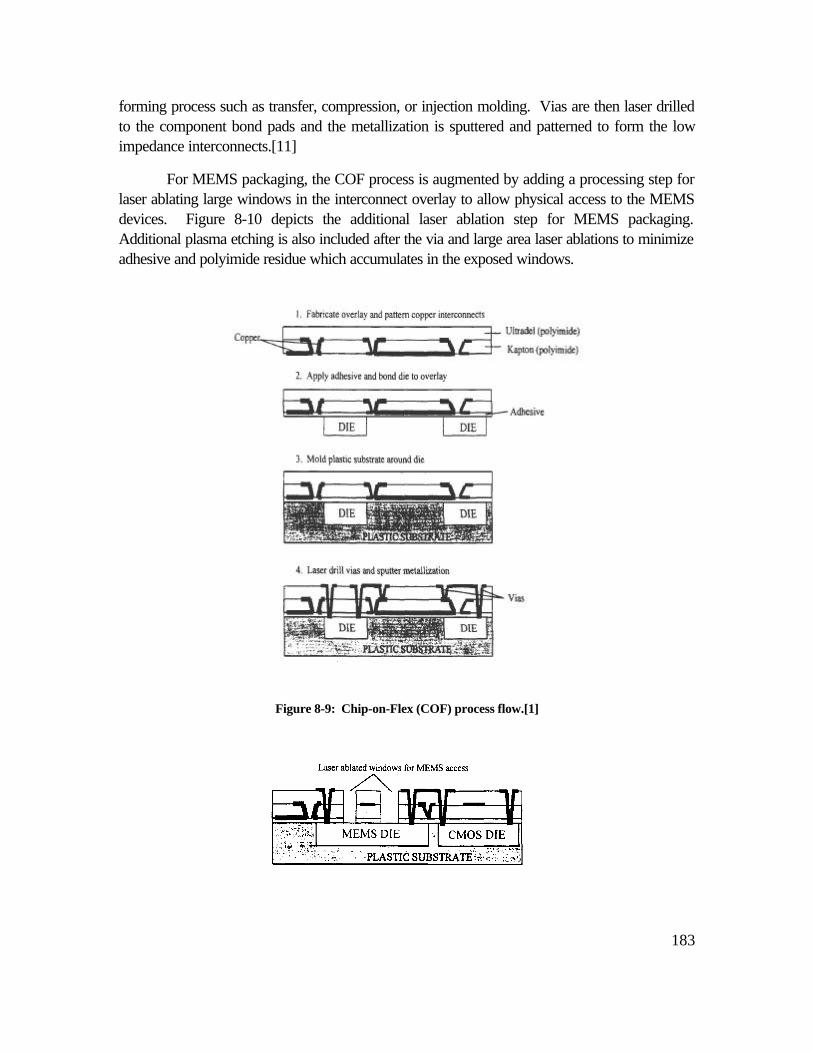
183
forming process such as transfer, compression, or injection molding. Vias are then laser drilledto the component bond pads and the metallization is sputtered and patterned to form the lowimpedance interconnects.[11]
For MEMS packaging, the COF process is augmented by adding a processing step forlaser ablating large windows in the interconnect overlay to allow physical access to the MEMSdevices. Figure 8-10 depicts the additional laser ablation step for MEMS packaging.Additional plasma etching is also included after the via and large area laser ablations to minimizeadhesive and polyimide residue which accumulates in the exposed windows.
Figure 8-9: Chip-on-Flex (COF) process flow.[1]
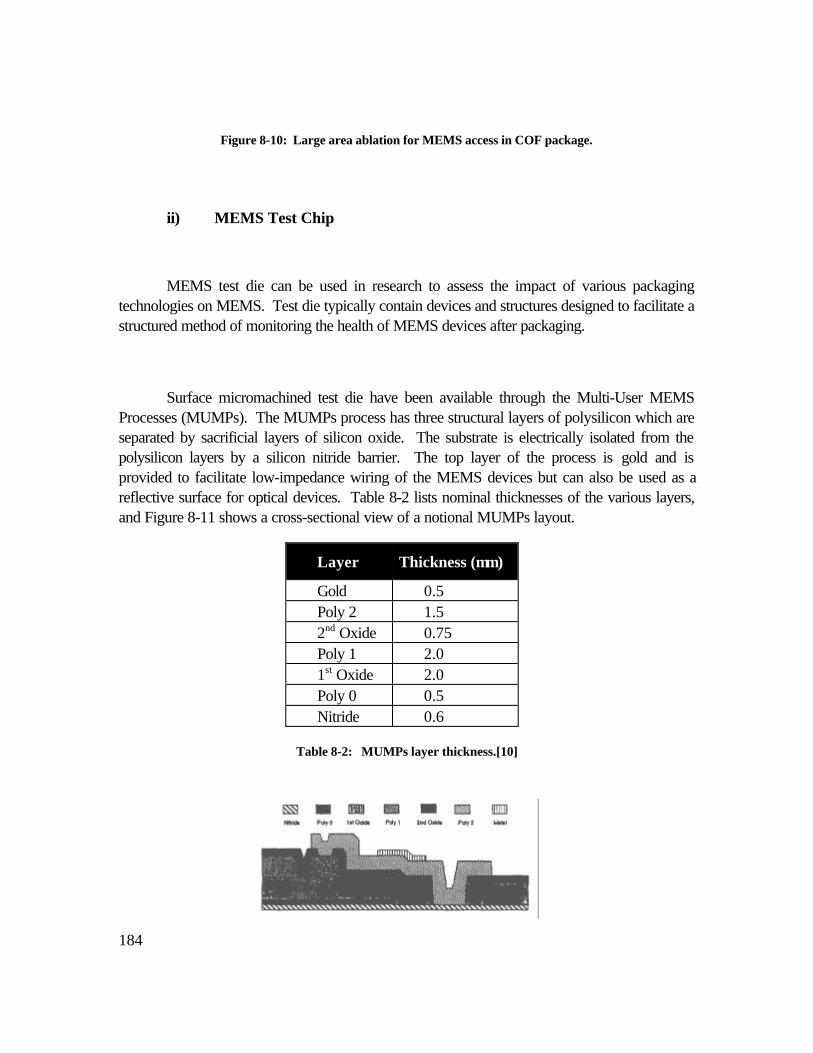
184
Figure 8-10: Large area ablation for MEMS access in COF package.
ii) MEMS Test Chip
MEMS test die can be used in research to assess the impact of various packagingtechnologies on MEMS. Test die typically contain devices and structures designed to facilitate astructured method of monitoring the health of MEMS devices after packaging.
Surface micromachined test die have been available through the Multi-User MEMSProcesses (MUMPs). The MUMPs process has three structural layers of polysilicon which areseparated by sacrificial layers of silicon oxide. The substrate is electrically isolated from thepolysilicon layers by a silicon nitride barrier. The top layer of the process is gold and isprovided to facilitate low-impedance wiring of the MEMS devices but can also be used as areflective surface for optical devices. Table 8-2 lists nominal thicknesses of the various layers,and Figure 8-11 shows a cross-sectional view of a notional MUMPs layout.
Layer Thickness (µm)
Gold 0.5Poly 2 1.52nd Oxide 0.75Poly 1 2.01st Oxide 2.0Poly 0 0.5Nitride 0.6
Table 8-2: MUMPs layer thickness.[10]
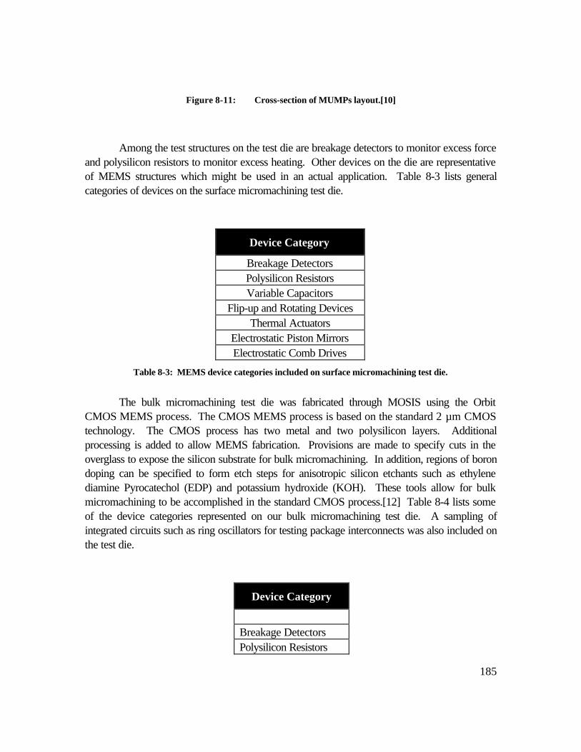
185
Figure 8-11: Cross-section of MUMPs layout.[10]
Among the test structures on the test die are breakage detectors to monitor excess forceand polysilicon resistors to monitor excess heating. Other devices on the die are representativeof MEMS structures which might be used in an actual application. Table 8-3 lists generalcategories of devices on the surface micromachining test die.
Device Category
Breakage DetectorsPolysilicon ResistorsVariable Capacitors
Flip-up and Rotating DevicesThermal Actuators
Electrostatic Piston MirrorsElectrostatic Comb Drives
Table 8-3: MEMS device categories included on surface micromachining test die.
The bulk micromachining test die was fabricated through MOSIS using the OrbitCMOS MEMS process. The CMOS MEMS process is based on the standard 2 µm CMOStechnology. The CMOS process has two metal and two polysilicon layers. Additionalprocessing is added to allow MEMS fabrication. Provisions are made to specify cuts in theoverglass to expose the silicon substrate for bulk micromachining. In addition, regions of borondoping can be specified to form etch steps for anisotropic silicon etchants such as ethylenediamine Pyrocatechol (EDP) and potassium hydroxide (KOH). These tools allow for bulkmicromachining to be accomplished in the standard CMOS process.[12] Table 8-4 lists someof the device categories represented on our bulk micromachining test die. A sampling ofintegrated circuits such as ring oscillators for testing package interconnects was also included onthe test die.
Device Category
Breakage DetectorsPolysilicon Resistors
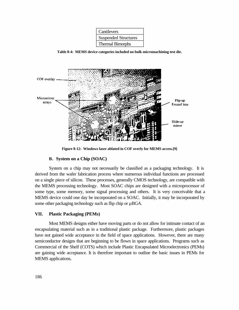
186
CantileversSuspended StructuresThermal Bimorphs
Table 8-4: MEMS device categories included on bulk micromachining test die.
Figure 8-12: Windows laser ablated in COF overly for MEMS access.[9]
B. System on a Chip (SOAC)
System on a chip may not necessarily be classified as a packaging technology. It isderived from the wafer fabrication process where numerous individual functions are processedon a single piece of silicon. These processes, generally CMOS technology, are compatible withthe MEMS processing technology. Most SOAC chips are designed with a microprocessor ofsome type, some memory, some signal processing and others. It is very conceivable that aMEMS device could one day be incorporated on a SOAC. Initially, it may be incorporated bysome other packaging technology such as flip chip or µBGA.
VII. Plastic Packaging (PEMs)
Most MEMS designs either have moving parts or do not allow for intimate contact of anencapsulating material such as in a traditional plastic package. Furthermore, plastic packageshave not gained wide acceptance in the field of space applications. However, there are manysemiconductor designs that are beginning to be flown in space applications. Programs such asCommercial of the Shelf (COTS) which include Plastic Encapsulated Microelectronics (PEMs)are gaining wide acceptance. It is therefore important to outline the basic issues in PEMs forMEMS applications.
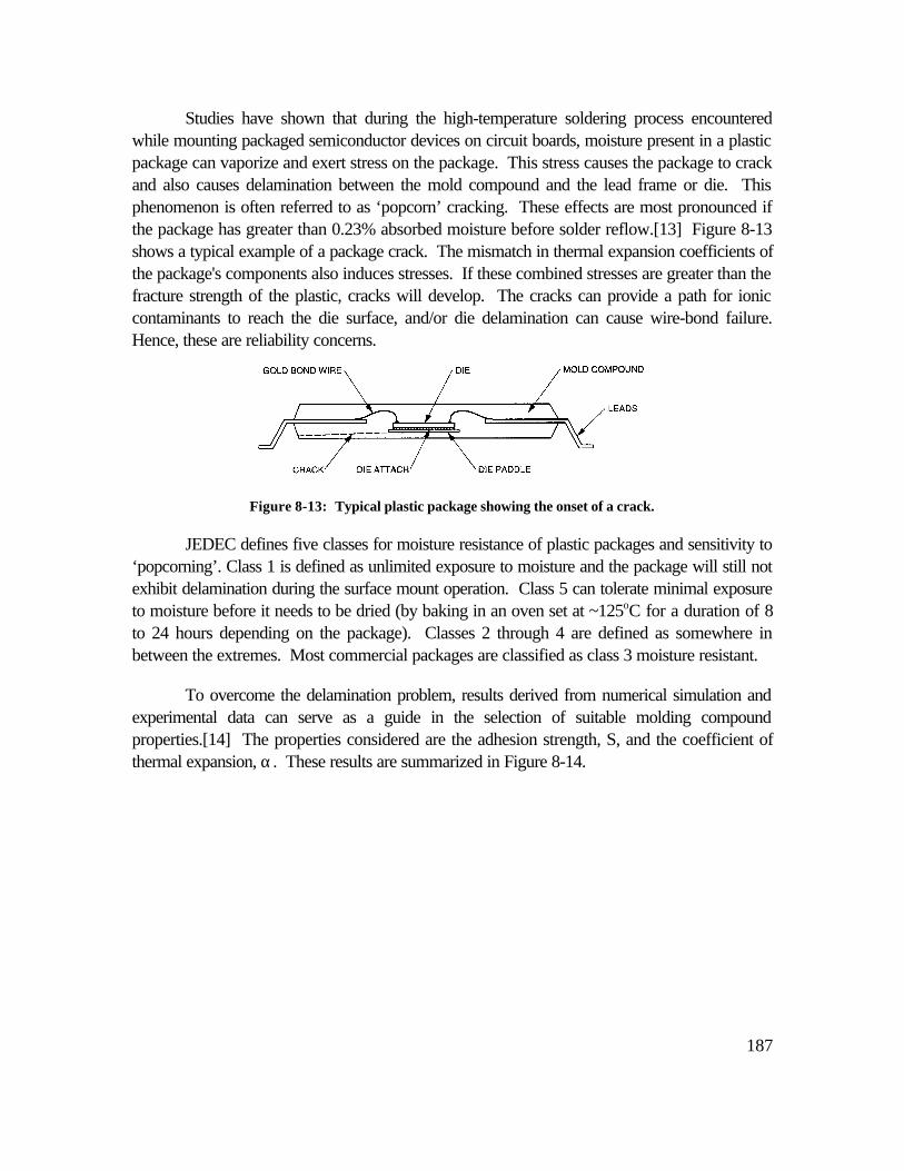
187
Studies have shown that during the high-temperature soldering process encounteredwhile mounting packaged semiconductor devices on circuit boards, moisture present in a plasticpackage can vaporize and exert stress on the package. This stress causes the package to crackand also causes delamination between the mold compound and the lead frame or die. Thisphenomenon is often referred to as ‘popcorn’ cracking. These effects are most pronounced ifthe package has greater than 0.23% absorbed moisture before solder reflow.[13] Figure 8-13shows a typical example of a package crack. The mismatch in thermal expansion coefficients ofthe package's components also induces stresses. If these combined stresses are greater than thefracture strength of the plastic, cracks will develop. The cracks can provide a path for ioniccontaminants to reach the die surface, and/or die delamination can cause wire-bond failure.Hence, these are reliability concerns.
Figure 8-13: Typical plastic package showing the onset of a crack.
JEDEC defines five classes for moisture resistance of plastic packages and sensitivity to‘popcorning’. Class 1 is defined as unlimited exposure to moisture and the package will still notexhibit delamination during the surface mount operation. Class 5 can tolerate minimal exposureto moisture before it needs to be dried (by baking in an oven set at ~125oC for a duration of 8to 24 hours depending on the package). Classes 2 through 4 are defined as somewhere inbetween the extremes. Most commercial packages are classified as class 3 moisture resistant.
To overcome the delamination problem, results derived from numerical simulation andexperimental data can serve as a guide in the selection of suitable molding compoundproperties.[14] The properties considered are the adhesion strength, S, and the coefficient ofthermal expansion, α. These results are summarized in Figure 8-14.
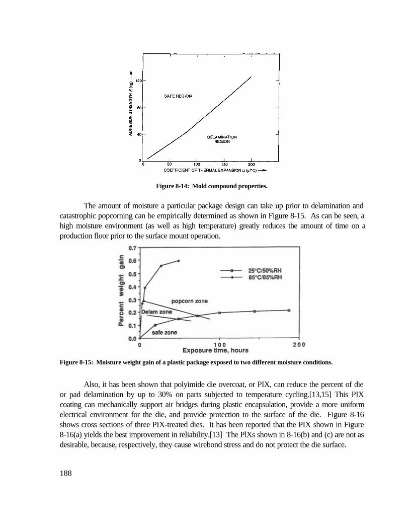
188
Figure 8-14: Mold compound properties.
The amount of moisture a particular package design can take up prior to delamination andcatastrophic popcorning can be empirically determined as shown in Figure 8-15. As can be seen, ahigh moisture environment (as well as high temperature) greatly reduces the amount of time on aproduction floor prior to the surface mount operation.
Figure 8-15: Moisture weight gain of a plastic package exposed to two different moisture conditions.
Also, it has been shown that polyimide die overcoat, or PIX, can reduce the percent of dieor pad delamination by up to 30% on parts subjected to temperature cycling.[13,15] This PIXcoating can mechanically support air bridges during plastic encapsulation, provide a more uniformelectrical environment for the die, and provide protection to the surface of the die. Figure 8-16shows cross sections of three PIX-treated dies. It has been reported that the PIX shown in Figure8-16(a) yields the best improvement in reliability.[13] The PlXs shown in 8-16(b) and (c) are not asdesirable, because, respectively, they cause wirebond stress and do not protect the die surface.
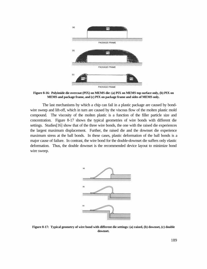
189
Figure 8-16: Polyimide die overcoat (PIX) on MEMS die: (a) PIX on MEMS top surface only, (b) PIX onMEMS and package frame, and (c) PIX on package frame and sides of MEMS only.
The last mechanisms by which a chip can fail in a plastic package are caused by bond-wire sweep and lift-off, which in turn are caused by the viscous flow of the molten plastic moldcompound. The viscosity of the molten plastic is a function of the filler particle size andconcentration. Figure 8-17 shows the typical geometries of wire bonds with different diesettings. Studies[16] show that of the three wire bonds, the one with the raised die experiencesthe largest maximum displacement. Further, the raised die and the downset die experiencemaximum stress at the ball bonds. In these cases, plastic deformation of the ball bonds is amajor cause of failure. In contrast, the wire bond for the double-downset die suffers only elasticdeformation. Thus, the double downset is the recommended device layout to minimize bondwire sweep.
Figure 8-17: Typical geometry of wire bond with different die settings: (a) raised, (b) downset, (c) doubledownset.
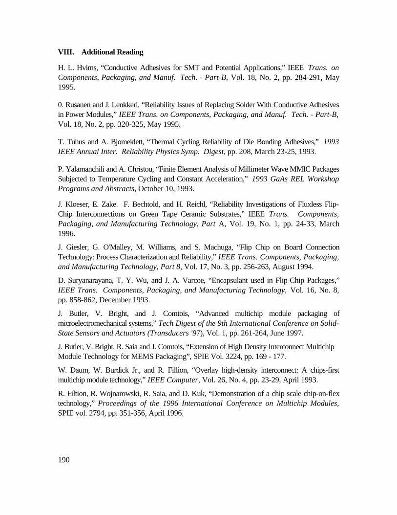
190
VIII. Additional Reading
H. L. Hvims, “Conductive Adhesives for SMT and Potential Applications,” IEEE Trans. onComponents, Packaging, and Manuf. Tech. - Part-B, Vol. 18, No. 2, pp. 284-291, May1995.
0. Rusanen and J. Lenkkeri, “Reliability Issues of Replacing Solder With Conductive Adhesivesin Power Modules,” IEEE Trans. on Components, Packaging, and Manuf. Tech. - Part-B,Vol. 18, No. 2, pp. 320-325, May 1995.
T. Tuhus and A. Bjomeklett, “Thermal Cycling Reliability of Die Bonding Adhesives,” 1993IEEE Annual Inter. Reliability Physics Symp. Digest, pp. 208, March 23-25, 1993.
P. Yalamanchili and A. Christou, “Finite Element Analysis of Millimeter Wave MMIC PackagesSubjected to Temperature Cycling and Constant Acceleration,” 1993 GaAs REL WorkshopPrograms and Abstracts, October 10, 1993.
J. Kloeser, E. Zake. F. Bechtold, and H. Reichl, “Reliability Investigations of Fluxless Flip-Chip Interconnections on Green Tape Ceramic Substrates,” IEEE Trans. Components,Packaging, and Manufacturing Technology, Part A, Vol. 19, No. 1, pp. 24-33, March1996.
J. Giesler, G. O'Malley, M. Williams, and S. Machuga, “Flip Chip on Board ConnectionTechnology: Process Characterization and Reliability,” IEEE Trans. Components, Packaging,and Manufacturing Technology, Part 8, Vol. 17, No. 3, pp. 256-263, August 1994.
D. Suryanarayana, T. Y. Wu, and J. A. Varcoe, “Encapsulant used in Flip-Chip Packages,”IEEE Trans. Components, Packaging, and Manufacturing Technology, Vol. 16, No. 8,pp. 858-862, December 1993.
J. Butler, V. Bright, and J. Comtois, “Advanced multichip module packaging ofmicroelectromechanical systems,” Tech Digest of the 9th International Conference on Solid-State Sensors and Actuators (Transducers '97), Vol. 1, pp. 261-264, June 1997.
J. Butler, V. Bright, R. Saia and J. Comtois, “Extension of High Density Interconnect MultichipModule Technology for MEMS Packaging”, SPIE Vol. 3224, pp. 169 - 177.
W. Daum, W. Burdick Jr., and R. Fillion, “Overlay high-density interconnect: A chips-firstmultichip module technology,” IEEE Computer, Vol. 26, No. 4, pp. 23-29, April 1993.
R. Filtion, R. Wojnarowski, R. Saia, and D. Kuk, “Demonstration of a chip scale chip-on-flextechnology,” Proceedings of the 1996 International Conference on Multichip Modules,SPIE vol. 2794, pp. 351-356, April 1996.
191
J. Marshall, M. Parameswaran, M. Zaghloul, and M. Gaitan, “High-level CAD meldsmicromachined devices with foundries,” Circuits and Devices, Vol. 9, no. 6, pp. 10- 17,November 1992.
T. M. Moore and S. J. Kelsall, “The Impact of Delamination on Stress-Induced andContamination-Related Failure in Surface Mount ICs,” 1992 IEEE Annual Int. ReliabilityPhysics Symp. Proc., pp. 169-176, March 31-April 2, 1992.
A. A. 0. Tay, G. L. Tam, and T. B. Lim, “Predicting Delamination in Plastic IC Packages andDetermining Suitable Mold Compound Properties,” IEEE Trans. Components, Packaging,and Manufacturing Technology-Part 8, Vol. 17, No. 2, pp. 201-208, May 1994.
W. J. Roesch and A. L. Rubalcava, “GaAs IC Reliability in Plastic Packages,” 1995 GaAsReliability Workshop Programs and Abstracts, pp. 25-30, October 29, 1995.
A. A. 0. Tay, K. S. Yeo, and J. H. Wu, “The Effect of Wirebond Geometry and Die Setting onWire Sweep,” IEEE Trans. Components, Packaging, and Manufacturing Technology-Part B, Vol. 18, No. 1, pp. 201-209, February 1995.

192
193
Chapter 9: Test Structures
B. Stark
As previously mentioned, there is a serious debate within the MEMS community aboutthe materials properties of thin films. Accurate knowledge of these properties is critical forassessing the long-term reliability of MEMS devices. In order to measure thin film propertiesand make these basic assessments, test structures are needed. Test structures are, in theirsimplest sense, sensors. Instead of sensing external forces they sense the environment they areexposed to. Most fabrication facilities utilize test structures on their production line to assess thequality of their process.
In order to ensure reliable operation, test structures that characterize both the processand materials used to manufacture devices must be made concurrently. It is the analysis of thesetest structures that will enable systems engineers to incorporate MEMS into their designs with ahigh degree of confidence in their reliability. This chapter describes some of the basic teststructures used and their implications.
I. Technology Characterization Vehicle
A technology characterization vehicle, or TCV, is a structure that is used to evaluate theeffects of specific failure mechanisms on a technology. Typically the devices used in TCVs willbe derived from a standard library of device elements. This library might include cantileverbeams, membranes, and other structures that are used commonly in MEMS technology.
Technology characterization vehicles will be subjected to a given test in order to predictfailure from particular failure mechanisms. These structures should be used to determine anestimate of the mean-time-to-failure and failure probability models. The use of these devices isa critical part of the qualification process, as they provide a wealth of knowledge about thereliability of structures. TCVs should be packaged and handled exactly the same as otherMEMS so that the information that they provide is as accurate as possible.
II. Standard Evaluation Devices
A standard evaluation device, or SED, is similar to a TCV except that an SED is notconstructed out of typical design elements, but is instead constructed out of actual sensor andactuator structures. Usually the SED is a less complicated version of a completed device andprovides reliability information about the performance of devices instead of structures. In agood quality control process, the parameters measured in different SEDs will be comparedacross wafers and lots to determine reliability characteristics of production runs. As in TCVs,SEDs should be treated in the same fashion as a fully functional device.
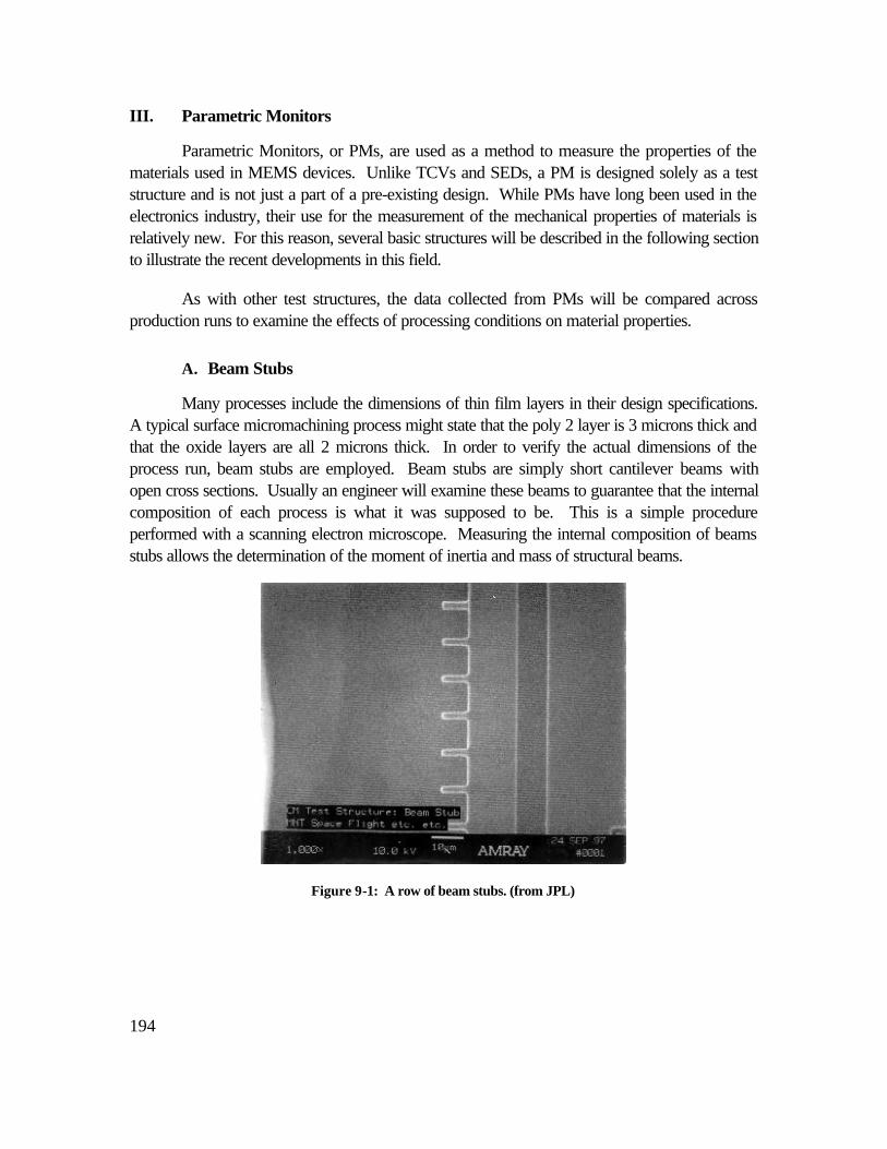
194
III. Parametric Monitors
Parametric Monitors, or PMs, are used as a method to measure the properties of thematerials used in MEMS devices. Unlike TCVs and SEDs, a PM is designed solely as a teststructure and is not just a part of a pre-existing design. While PMs have long been used in theelectronics industry, their use for the measurement of the mechanical properties of materials isrelatively new. For this reason, several basic structures will be described in the following sectionto illustrate the recent developments in this field.
As with other test structures, the data collected from PMs will be compared acrossproduction runs to examine the effects of processing conditions on material properties.
A. Beam Stubs
Many processes include the dimensions of thin film layers in their design specifications.A typical surface micromachining process might state that the poly 2 layer is 3 microns thick andthat the oxide layers are all 2 microns thick. In order to verify the actual dimensions of theprocess run, beam stubs are employed. Beam stubs are simply short cantilever beams withopen cross sections. Usually an engineer will examine these beams to guarantee that the internalcomposition of each process is what it was supposed to be. This is a simple procedureperformed with a scanning electron microscope. Measuring the internal composition of beamsstubs allows the determination of the moment of inertia and mass of structural beams.
Figure 9-1: A row of beam stubs. (from JPL)
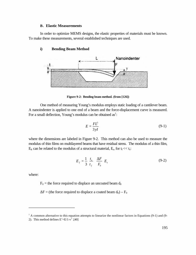
195
B. Elastic Measurements
In order to optimize MEMS designs, the elastic properties of materials must be known.To make these measurements, several established techniques are used.
i) Bending Beam Method
Figure 9-2: Bending beam method. (from [126])
One method of measuring Young’s modulus employs static loading of a cantilever beam.A nanoindenter is applied to one end of a beam and the force-displacement curve is measured.For a small deflection, Young’s modulus can be obtained as1:
yIFL
E3
3
=
where the dimensions are labeled in Figure 9-2. This method can also be used to measure themodulus of thin films on multilayered beams that have residual stress. The modulus of a thin film,Ef, can be related to the modulus of a structural material, Es, for tf << ts:
sf
sf E
FF
tt
E
∆
=
031
where:
F0 = the force required to displace an uncoated beam d0
∆F = (the force required to displace a coated beam d0) – F0
1 A common alternative to this equation attempts to linearize the nonlinear factors in Equations (9-1) and (9-2). This method defines E’=E/1-ν2 .[40]
(9-1)
(9-2)
y
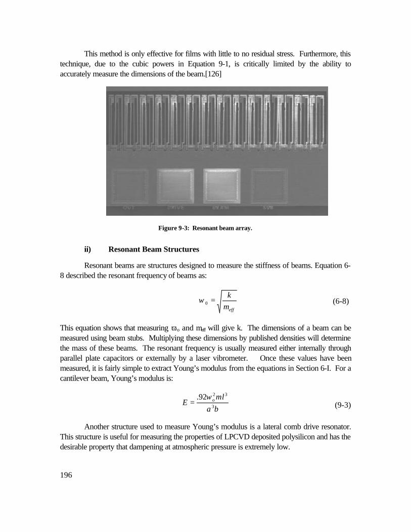
196
This method is only effective for films with little to no residual stress. Furthermore, thistechnique, due to the cubic powers in Equation 9-1, is critically limited by the ability toaccurately measure the dimensions of the beam.[126]
Figure 9-3: Resonant beam array.
ii) Resonant Beam Structures
Resonant beams are structures designed to measure the stiffness of beams. Equation 6-8 described the resonant frequency of beams as:
This equation shows that measuring ωo and meff will give k. The dimensions of a beam can bemeasured using beam stubs. Multiplying these dimensions by published densities will determinethe mass of these beams. The resonant frequency is usually measured either internally throughparallel plate capacitors or externally by a laser vibrometer. Once these values have beenmeasured, it is fairly simple to extract Young’s modulus from the equations in Section 6-I. For acantilever beam, Young’s modulus is:
baml
E o3
3292. ω=
Another structure used to measure Young’s modulus is a lateral comb drive resonator.This structure is useful for measuring the properties of LPCVD deposited polysilicon and has thedesirable property that dampening at atmospheric pressure is extremely low.
effmk
=0ω (6-8)
(9-3)
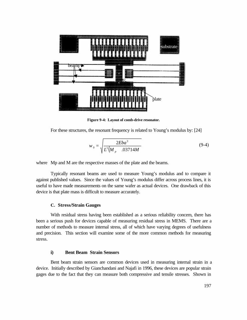
197
Figure 9-4: Layout of comb-drive resonator.
For these structures, the resonant frequency is related to Young’s modulus by: [24]
( )MMLEba
p 03714.2
3
3
0 +=ω
where Mp and M are the respective masses of the plate and the beams.
Typically resonant beams are used to measure Young’s modulus and to compare itagainst published values. Since the values of Young’s modulus differ across process lines, it isuseful to have made measurements on the same wafer as actual devices. One drawback of thisdevice is that plate mass is difficult to measure accurately.
C. Stress/Strain Gauges
With residual stress having been established as a serious reliability concern, there hasbeen a serious push for devices capable of measuring residual stress in MEMS. There are anumber of methods to measure internal stress, all of which have varying degrees of usefulnessand precision. This section will examine some of the more common methods for measuringstress.
i) Bent Beam Strain Sensors
Bent beam strain sensors are common devices used in measuring internal strain in adevice. Initially described by Gianchandani and Najafi in 1996, these devices are popular straingages due to the fact that they can measure both compressive and tensile stresses. Shown in
(9-4)
substrate
plate
beams
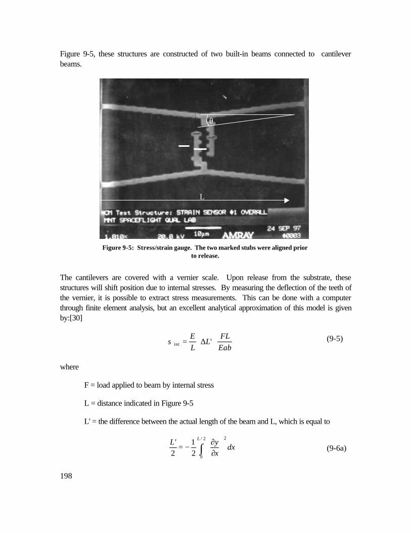
198
Figure 9-5, these structures are constructed of two built-in beams connected to cantileverbeams.
The cantilevers are covered with a vernier scale. Upon release from the substrate, thesestructures will shift position due to internal stresses. By measuring the deflection of the teeth ofthe vernier, it is possible to extract stress measurements. This can be done with a computerthrough finite element analysis, but an excellent analytical approximation of this model is givenby:[30]
+∆=
EabFL
LLE
'intσ
where
F = load applied to beam by internal stress
L = distance indicated in Figure 9-5
L' = the difference between the actual length of the beam and L, which is equal to
∫
∂∂
−=2/
0
2
21
2' L
dxxyL
Figure 9-5: Stress/strain gauge. The two marked stubs were aligned priorto release.
(9-5)
(9-6a)
L
θa
199
When solved, L' becomes:
( )( ) [ ])cosh()cosh(2)sinh(24
tan' 22
2
kLHkLHkLkLHkLHk
L a +−+−+=θ
in
tension and
( )( ) [ ])sin()cos(2)sin(24
tan' 22
2
kLGkLGkLkLGkLGk
L a −−+++=θ
in compression
where
G = tan(kL/4)
H = tanh(kL/4)
k = EIF
The displacement y is related to k, and thus L' by the relationship
( )
=
4tanh
tan2
kLk
y aTension
θ
( )
=
4tan
tan2
kLk
y anCompressio
θ
These structures are limited in resolution by the minimum feature size of a technology.While these limitations are usually small, they could be a serious problem on some largertechnologies, such as LIGA. Out-of-plane displacements caused by stress gradients and non-uniform beam thickness can inhibit device sensitivity. Ultimately these devices will have difficultybeing accurate below 10 MPa.[30]
ii) Cantilever Beams
Cantilever beams are commonly used as a simple way to measure internal stress. Sincemost technologies utilize cantilever beams, it is a relatively simple step to place extra cantileverbeams onto a device for stress measurement. One method uses cantilever beam deflection tomeasure stress. Since most stresses on these devices causes non-planar displacement, a systemthat can measure z-axis deflection can measure stress. With a multitude of laser interferometery
(9-6b)
(9-6c)
(9-8)
(9-7)
200
systems now available to measure surface topology, these measurements are easy to make bothquickly and accurately.
Since internal stress is rarely uniform, but is instead a function of material thickness,many researchers are interested in the stress gradient within a material. The stress gradient iscalculated by looking at the change in stress over the change over film thickness. For acantilever beam, the stress gradient can be analytically approximated by:
2)1(2
lyE
dtd
νσ
−=
where
y = non-planar deflection of the cantilever tip
t = thickness of the film
l = length of the cantilever
While this equation assumes a linearly varying stress field, this is not an unrealisticassumption. Although this equation does not take into account many of the irregularitiesconsidered in a finite element analysis, it does offer a good order of magnitude calculation for thestress field within thin films.
iii) Buckling Beam Structures
Many test structures take advantage of buckling behavior in beams to measure stresses.The stress needed to buckle a doubly clamped beam is defined as:
2
22
3LEh
bπ
σ −=
where
h = beam thickness
L = beam length
As such, for structural beams, buckling is a function of stress levels. Designers haveused this fact in creating arrays of these beams. Each beam in the array has differentdimensions, with a corresponding buckling stress. By examining the beams after release it ispossible to measure stress by observing the beam with the largest σb that buckled. This
(9-9)
(9-10)
201
technique is a very accurate way of measuring compressive stresses in beams. With longerbeams having a σb<1 MPa, these arrays can be quite sensitive.
For tensile stresses, another set of test structures called Guckel Rings, has beendeveloped to utilize buckling in measuring stresses. Guckel Rings are also used in arrays andthe critical buckling load is defined by:[130,138]
2
22
)(12 RRgEh
bπ
σ =
where
R = ring radius
g(R) = a function of inner and outer ring radius ≤ 0.918
iv) Substrate Analysis
One method to measure stress in thin films does not use actual test structures as they arecommonly known. Instead this technique uses substrate deformation to measure stress. This isdone by measuring the radius of curvature of the substrate before and after deposition of a thinfilm. Then the Stoney equation can relate these measurements to the residual stress:[139, 140]
−
−=
fo
sr RRt
Et 11)1(6
2
νσ
where
Ro, Rf = initial and final radii
t = thin film thickness
ts = wafer thickness
This method provides good residual stress measurements down to about 10 MPa.Below this level, boundary conditions and gravity affect measurement accuracy. The majorlimitation of this method is that it does not provide direct measurement of stresses in finisheddevices.
(9-11)
(9-12)
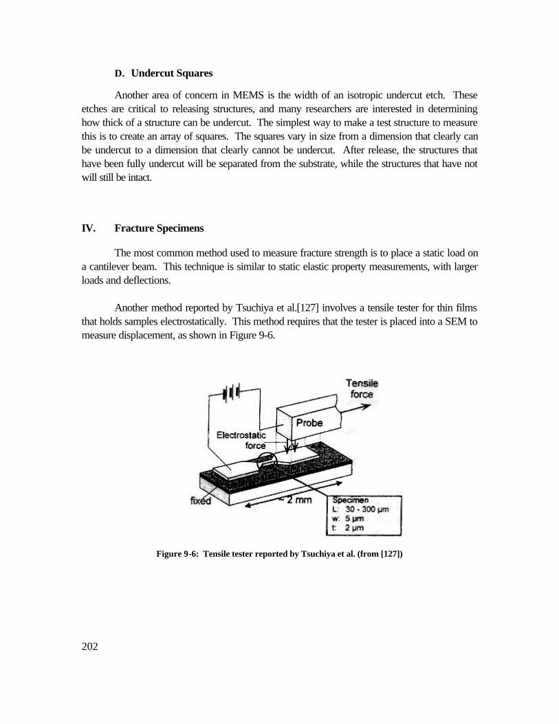
202
D. Undercut Squares
Another area of concern in MEMS is the width of an isotropic undercut etch. Theseetches are critical to releasing structures, and many researchers are interested in determininghow thick of a structure can be undercut. The simplest way to make a test structure to measurethis is to create an array of squares. The squares vary in size from a dimension that clearly canbe undercut to a dimension that clearly cannot be undercut. After release, the structures thathave been fully undercut will be separated from the substrate, while the structures that have notwill still be intact.
IV. Fracture Specimens
The most common method used to measure fracture strength is to place a static load ona cantilever beam. This technique is similar to static elastic property measurements, with largerloads and deflections.
Another method reported by Tsuchiya et al.[127] involves a tensile tester for thin filmsthat holds samples electrostatically. This method requires that the tester is placed into a SEM tomeasure displacement, as shown in Figure 9-6.
Figure 9-6: Tensile tester reported by Tsuchiya et al. (from [127])

203
A less complicated method described by Greek et al. is to use a probe tip connected toa thin beam. By applying a force to the probe, it is possible to measure fracturestress.[128,129]
Figure 9-7: Tensile tester reported by Greek et al. (from [128])
A. Thermal Properties Measurements
The thermal properties of MEMS are important for a number of applications. It isimportant to accurately know the linear expansion coefficient and the thermal conductivity forcertain devices. There are several methods to do this.
i) Cantilever Beam Method
A cantilever beam can be used to measure the linear coefficient of expansion. Bymeasuring the change in curvature, ∆(dy/dx), for a given change in temperature, it is possible todetermine the linear coefficient of expansion of a thin film material, αf:[131]
( ) ( )T
CT
dxdy sf ∆
−=∆∆
αα
where
αs = the coefficient of expansion of the substrate (a well-known value)
++=
ss
ff
s
f
ff
ss
tE
tE
t
t
tEtE
C 416
2
ii) Thin Film Heater
One popular method for measuring the thermal conductivity of a film employs a thin filmheater attached to the free end of a cantilever beam. The temperature gradient between theheater and the fixed end of the cantilever can be determined via a row of thermocouples, asshown in Figure 9-8.[129,132,133]
(9-13)
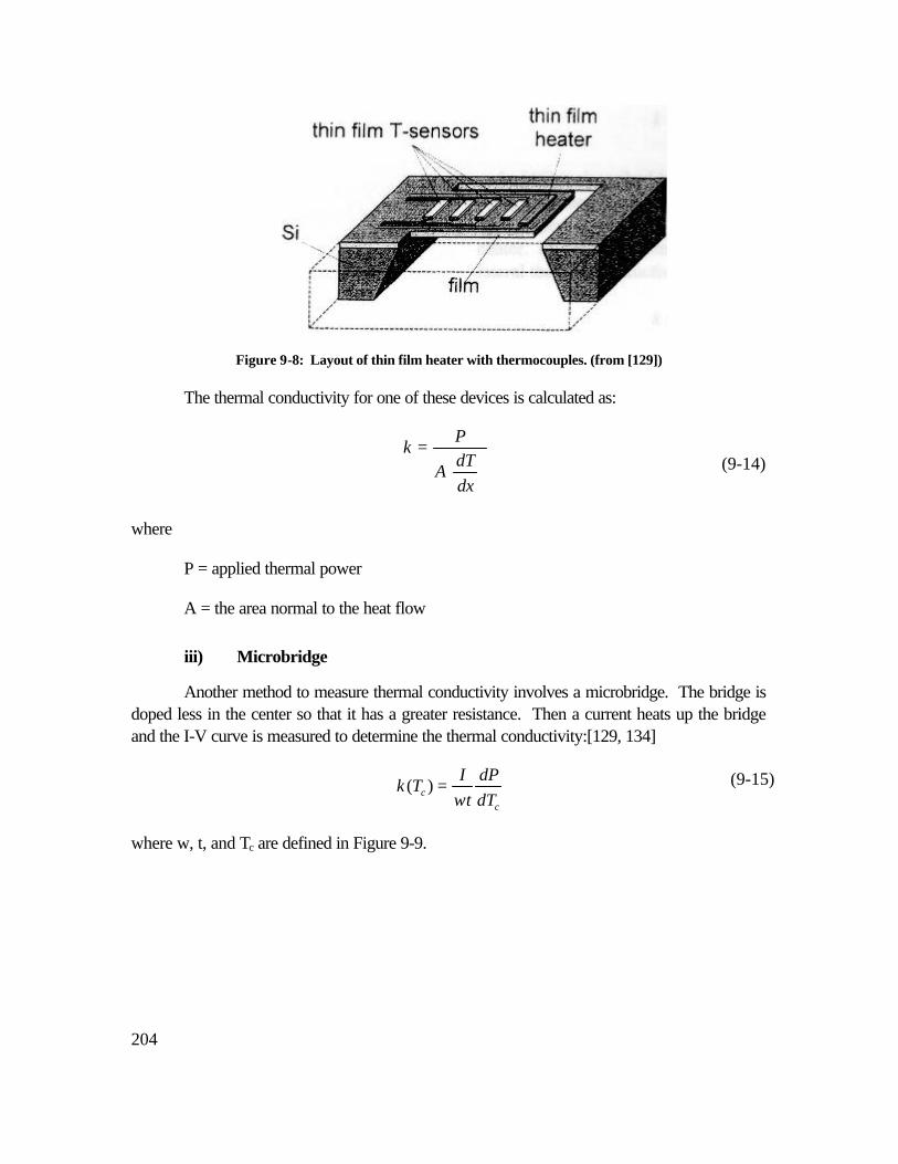
204
Figure 9-8: Layout of thin film heater with thermocouples. (from [129])
The thermal conductivity for one of these devices is calculated as:
=
dxdT
A
Pk
where
P = applied thermal power
A = the area normal to the heat flow
iii) Microbridge
Another method to measure thermal conductivity involves a microbridge. The bridge isdoped less in the center so that it has a greater resistance. Then a current heats up the bridgeand the I-V curve is measured to determine the thermal conductivity:[129, 134]
cc dT
dPwtI
Tk =)(
where w, t, and Tc are defined in Figure 9-9.
(9-14)
(9-15)
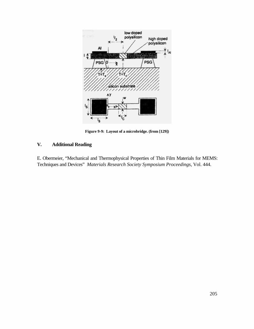
205
Figure 9-9: Layout of a microbridge. (from [129])
V. Additional Reading
E. Obermeier, “Mechanical and Thermophysical Properties of Thin Film Materials for MEMS:Techniques and Devices” Materials Research Society Symposium Proceedings, Vol. 444.

206
207
Chapter 10: Qualification Testing Protocols for MEMS
B. Stark and S. Kayali
This guideline has offered detailed physical analysis of the distinct parts and materialsused to manufacture a MEMS device. In this chapter, all the information presented will be tiedtogether through the common thread of space qualification. It must be primarily understood thatthis guideline is not, and was never intended to be, a rigid set of specifications. It is instead arecommendation of qualification methods. Clearly with the vast array of devices used in theindustry, it would be difficult to qualify the individual tests needed on a given device.
The proper use of this guide requires referencing to all the chapters. The specifics ofqualifying a device depend upon the specifics of the process, materials, and structures in adevice. The reason that specific standards were not set for MEMS in space is that many peoplewithin the electronics community have complained that these standards limit their devicedevelopment and do not recognize that some tests on some devices are unnecessary. A furtherproblem with standards is that they often do not take into account mission requirements. It isthe ultimate job of the mission designers to determine the thermal ranges and radiation levelsexpected during the mission. To set these ahead of time, without this foreknowledge, canrequire expensive overdesigning of parts on short term missions and be too lenient on parts usedon longer missions.
In order to improve reliability, qualification should begin as early as possible. Historyhas shown that the reliability of a device will fluctuate over its development cycle as shown inFigure 10-1.
208
The initial low reliability of prototypes can be attributed to a myriad of causes fromdesign flaws to manufacturing process problems, with a number of other environmental andhandling issues having an impact. After this initial period, reliability improves from refinements indevice manufacture and from the identification and eradication of predominant failure modes.Once a device is placed into production, there is a regression of reliability stemming from thecompromises made to transfer a device from research production to a full scale manufacturingline. With eventual improvements in production processing, reliability should approach thepotential device reliability.
These reliability fluctuations from design to production can be minimized byincorporating statistical process control methodologies into device fabrication and by performinglife-testing. This step will force reliability improvements to coincide with device production andwill ultimately lead to a more reliable device that can be brought to market much quicker thanwould be otherwise expected. As such, this chapter provides the methods necessary to bothlimit this reliability swing during device development and to improve long term device reliability.
There is a four-step procedure followed by most satellite manufacturers which includessome practices recommended by Qualified Manufacturers Listing, or QML, programs. Thesesteps of Process Qualification, Product Qualification, Product Acceptance, and CompanyCertification, are summarized in Figure 10-2. Process Qualification concerns a procedure the
PREDICTED ORPOTENTIALRELIABILITY
RELIABILITY OFINITIALPROTOTYPE
RELIABILITY OFINITIALPRODUCTION
RELIABILITYGROWTH DURINGDEVELOPMENT
RELIABILITYGROWTH DURINGPRODUCTION
PRO
DU
CT
RE
LIA
BIL
ITY
DEVICE DEVELOPMENT
Figure 10-1: Reliability over the development cycle.
Figure 2-2: Product Development Cycle
209
manufacturers should follow to assure the quality, uniformity, and reproducibility of MEMS froma specific fabrication process. Product Qualification encompasses a set of simulations andmeasurements to establish the mechanical, electrical, thermal, and reliability characteristics of aparticular device. Product Acceptance is a series of tests performed on the deliverable devicethat are designed to ensure that a part meets the program requirements and to provide specificreliability information pertinent to that product. Company Certification focuses on theprocedures and management controls that a manufacturer should have in place to assure thequality of their MEMS devices.
PROCESSDEVELOPMENTWAFER FAB DEVELOPMENTPARAMETRICMONITORSDESIGN RULEDEVELOPMENTLAYOUT RULEDEVELOPMENTWAFER LEVELTESTSTECHNOLOGYCHARACTERIZATIONAND STANDARD EVALUATIONTEST STRCUTURESSTARTINGMATERIALSCONTROLESDCHARACTERIZATION
PROCESS QUALIFICATION(SECTION 10-I)
DESIGNMODELLAYOUT
DESIGNVERIFICATION
THERMALCHARACTERIZATIONMECHANICALCHARACTERIZATIONESD SENSITIVITYVOLTAGE RAMPTEMP RAMPHIGH/LOWTEMP
PRODUCTCHARACTERIZATION
PRODUCT QUALIFICATION(SECTION 10-II)
WAFERACCPETANCETESTLOTACCEPTANCETESTPACKAGEDMEMS SCREEN
PRODUCT ACCEPTANCE(SECTION 10-III)
TECHNOLOGYREVIEWBOARDCONVERSION OF REQUIREMENTSMANUFACTURECONTROLEQUIPMENTCALIBRATIONTRAININGCORRECTIVEACTION PLANELECTROSTATICDISCHARGEPROGRAM (ESD)CLEANLINESS ANDATMOSPHERICCONTROLSRECORDRETENTIONINVENTORYCONTROLSTATISTICAL PROCESSCONTROL
COMPANY CERTIFICATION(SECTION 10-IV)
QUALIFICATION
Figure 10-2: Recommended qualification methodology.
Before these four steps are presented in any detail, one important aspect of MEMSqualification must be addressed. Although the manufacturer is ultimately responsible fordelivering a reliable MEMS, the overall system reliability is the domain of the MEMS user. For
1 Company Certification is a process that may only be possible in mature industries. Given the paucity ofMEMS foundries, it is uncertain if Company Certification is realizable. For this reason it is suggested, butcertainly not required that Company Certification be performed.
1
210
this reason, it is in the interest of both parties to understand the expected performancerequirements of both the MEMS and the system into which it will be inserted.
I. Process Qualification
Manufacturers who have standardized their production to a single technology will oftentry to qualify their entire production line. Through this process, the manufacturer attempts toshow that its entire production line is under control and operating efficiently. Furthermore, thisprocess enables the manufacturer to establish an electromechanical baseline to use in measuringperformance and reliability for all products coming off the line. The benefits of this process aretwofold. The manufacturer saves costs and time in the development of future devices, since thereliability and performance characteristics of the constituent parts of a device will have alreadybeen established. The user gains both the comfort of procuring parts from an established linewith a history of producing qualified parts and the cost savings inherent to a reducedqualification time.
The procedure of qualifying a production line is called process qualification. This isgenerally defined as the set of procedures that a manufacturer follows to demonstrate that theyhave control of the entire process of designing and fabricating a MEMS device using a specificprocess, which will usually be one of the processes listed in Chapter 5. This act addresses allaspects of production, including the acceptance of starting materials, documentation ofprocedures, implementation of handling procedures, and the establishment of lifetime and failuredata for devices fabricated with the process. Since the goal of process qualification is toprovide assurance that a particular process is under control and known to produce reliableparts, it needs to be performed only once, although a routine monitoring of the production line isstandard. It is important to understand that only the process and basic structures are beingqualified and that no reliability information is obtained for a particular MEMS design.
Although process qualification is intended to qualify a defined fabrication procedure anddevice family, it must be recognized that MEMS technology is evolving at an astounding rate,which requires the continual updating of fabrication procedures. Furthermore, minor changes inthe fabrication process to account for environmental variations, incoming material variations,continuous process improvement, or minor design modifications may be required. All of thesechanges are permitted and frequently occur under the direction of the TRB. Thus, maintainingthe status quo does not guarantee maintaining qualification.
DOES THE
PASS AUDIT Y
Y
Y
Y
Y
N
N
N
211
DEVELOP AND DOCUMENTSTANDARD WORKMANSHIP,
MANAGEMENT PROCEDURES,AND MATERIAL TRACKING PROCEDURES
DOCUMENT DESIGNSTANDARDS AND PROCESSING
PROCEDURES
FABRICATE STRUCTURESTO BE QUALFIED
DETERMINE DEVICEMODELS AND
SPECIFICATIONS OF STRUCTURES(FIG. 10-5)
MEMS PROCESS RELIABILITYEVALUATION
(FIG. 10-4)
PROCESS QUALIFIED
DEVELOP PROCESSING STEPS
ESTABLISH TRB
DETERMINE TYPE OF DEVICESTO BE FABRICATED
Figure 10-3: MEMS process qualification steps.
The internal documents and procedures used by most manufacturers are summarized inFigure 10-3. In addition to this, the QML program provides guidelines for process qualification.The first step in this procedure is to determine the family of devices to be fabricated and thetechnology that will be used in the fabrication. After this, the manufacturer will establish a TRBto control the process qualification procedure. After the processing steps have been definedand documented, the workmanship, management procedures, material tracking procedures, anddesign procedures should be documented. The information contained in the documentationdescribed the process domain that is being qualified.
PR
OC
ES
S F
LO
W
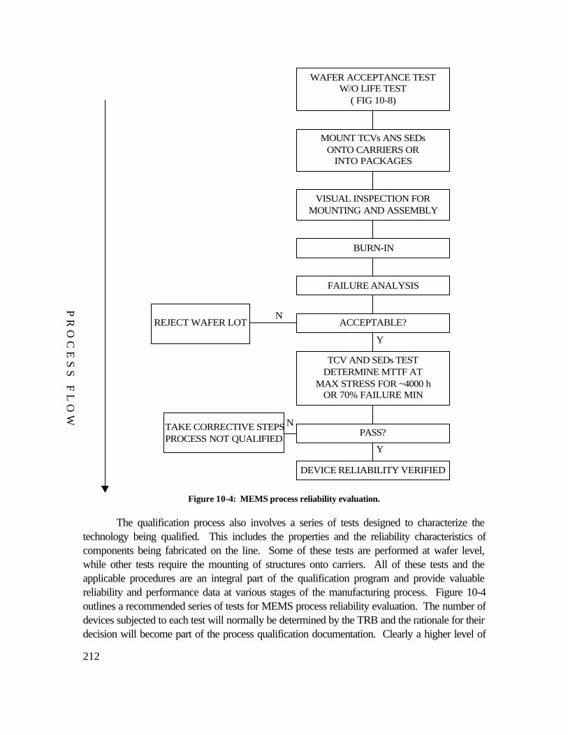
212
y
N
YN
Y
Y
REJECT WAFER LOTN
Y
TAKE CORRECTIVE STEPSPROCESS NOT QUALIFIED
DEVICE RELIABILITY VERIFIED
PASS?
TCV AND SEDs TESTDETERMINE MTTF AT
MAX STRESS FOR ~4000 hOR 70% FAILURE MIN
ACCEPTABLE?
FAILURE ANALYSIS
BURN-IN
VISUAL INSPECTION FORMOUNTING AND ASSEMBLY
MOUNT TCVs ANS SEDsONTO CARRIERS OR
INTO PACKAGES
WAFER ACCEPTANCE TESTW/O LIFE TEST
( FIG 10-8)
Figure 10-4: MEMS process reliability evaluation.
The qualification process also involves a series of tests designed to characterize thetechnology being qualified. This includes the properties and the reliability characteristics ofcomponents being fabricated on the line. Some of these tests are performed at wafer level,while other tests require the mounting of structures onto carriers. All of these tests and theapplicable procedures are an integral part of the qualification program and provide valuablereliability and performance data at various stages of the manufacturing process. Figure 10-4outlines a recommended series of tests for MEMS process reliability evaluation. The number ofdevices subjected to each test will normally be determined by the TRB and the rationale for theirdecision will become part of the process qualification documentation. Clearly a higher level of
PR
OC
ES
S F
LO
W
213
confidence exists if more structures are tested, but this must be balanced by the understandingthat, after a certain point, the incremental gain in confidence is more than offset by the increase incost related to the testing. Since the stability of the process is being determined as part of theprocess qualification, the manufacturer will typically fabricate and test components from severalwafer lots. Figure 10-5 provides a series of tests that are recommended to characterize theelectromechanical limitations of devices. The performance limitations obtained from these testsoften become the basis for limits incorporated into the design and layout rules.
One of the aspects of the processes qualification procedure to note is that the procedureis QML-like and therefore addresses topics similar to those of company certification. Themajor difference between the two is that company certification is performed by the customer,whereas process qualification is self-imposed by the manufacturer, often before customers areidentified. Items particular to process qualifications are described below.
A. Process Step Development
Although the Company Certification process is also fundamental to the processqualification procedure, the actual task of turning a bare wafer into a processed device is oftenthe only task associated with process qualification. While process qualification is actually moreinvolved, processing is the most critical step in process qualification and requires the most timeand resources to develop, In addition to this, it is important to recognize that the fabricationprocedures and devices processed on the line are the factors that separate one process fromanother. The first step towards process qualification is the documentation of all the stepsnecessary to produce a MEMS device. Although all of the steps in the fabrication processshould be documented, the details are typically considered proprietary by the manufacturer.Therefore the MEMS customer can expect to see a generalized process flow, but not a detailedaccount of each step necessary to reproduce a given product on another line.
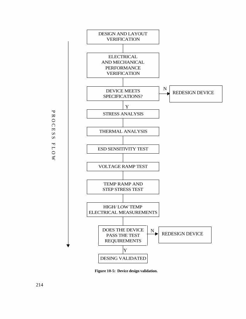
214
DESING VALIDATED
DOES THE DEVICEPASS THE TEST
REQUIREMENTS
HIGH/ LOW TEMPELECTRICAL MEASUREMENTS
TEMP RAMP ANDSTEP STRESS TEST
VOLTAGE RAMP TEST
ESD SENSITIVITY TEST
THERMAL ANALYSIS
STRESS ANALYSIS
DEVICE MEETSSPECIFICATIONS?
ELECTRICALAND MECHANICAL
PERFORMANCEVERIFICATION
DESIGN AND LAYOUTVERIFICATION
PR
OC
ES
S F
LO
W
REDESIGN DEVICEN
REDESIGN DEVICEN
Y
Y
Figure 10-5: Device design validation.

215
B. Wafer Fabrication Documentation
Once a process is qualified, reliability concerns may still arise from minor variations inthe process flow, environment, or starting materials. For this reason, all wafer fabrication stepsand conditions should be recorded by the manufacturer to maintain the repeatability of theproduct. Documentation of these steps and fabrication conditions should be maintained to traceany future quality or reliability concerns to a specific step. Although process travelers can beused to document the fabrication and manufacturing steps, they usually lack the detail necessaryto trace quality or reliability problems to specific fabrication steps. The wafer fabrication stepsthemselves and the documentation describing them are usually considered proprietary by themanufacturer.
C. Parametric Monitors
Parametric monitors are essential for monitoring a production line’s quality or continuousimprovement. PMs were fully described in Chapter 8; they are mentioned here only toemphasize the fact that the choice of the test structures is dependent on the process andtechnology being monitored. Therefore, this choice is a critical element in the processqualification procedure. The complete list of parametric monitors is usually combined into asingle list that is included on all wafers. The data obtained from the test structures will benormally stored in a database that permits the quick comparison of each wafer fabricated on theline to all of the other wafers. This permits determination of the process stability.
D. Design-Rule and Model Development
The reliability of MEMS fabricated on a qualified process will greatly depend onwhether or not they are fabricated from qualified structures according to prescribed rules. Inaddition to this, the standardization of the structures brings a certain degree of cost reduction.For this reason, part of the process qualification procedure is to determine and document designrules that are specific to the process. Typical information included will be the minimum featuresize, maximum etch hole separation, thickness of thin film materials, required overlap in layers,depth of dry etching. While individual processes will compile their own design rules, the listmust contain all information necessary to produce a working device. In addition to thisinformation, manufacturers should compile information on the properties of all the materials inthe process. Information such as Young’s modulus, fracture strength, intrinsic resistivity, straystress, and thermal characteristics, should be maintained by the manufacturer.
To use standard components in MEMS designs, models must be developed. Althoughsome commercial packages may include models, they need to be altered to fit measuredcharacteristics. Once standardized models are constructed, the chances of design success aregreatly increased.
216
E. Wafer Level Tests
The semiconductor industry strives to reduce production costs by shifting as muchtesting as possible to the earliest possible point in the production cycle in order to weed out badwafer lots before more time, and thus money, has been spent on them. The best strategyperforms wafer level tests that includes electromechanical characterization, test structurecharacterization, and environmental performance. Limitations may exist in the level of test detaildepending upon the device design and the manufacturer’s test capabilities. In general, wafer-level tests are performed, but they must be supplemented with other verifications, such as testfixture or in-package tests. Once agreement between the wafer-level and the package-leveltests has been established, the manufacturer may rely on the wafer-level tests for productionmonitoring.
F. TCV and SED Tests
One of the most important steps in the process-qualification procedure is to determinethe electromechanical, environmental, and reliability characteristics of devices fabricated withinthe domain of the process. This data is obtained through the characterization of TCV andSEDs, as shown in Figures 10-5 and 10-6. All data gathered from these tests should be storedby the TRB. In most cases, the success of a manufacturer in the qualifying process will dependon the data from these tests.
G. Starting Materials Control
The manufacturer should have a mechanism to assure the quality and characteristics ofevery starting material, from the wafers and chemicals used in the processing steps to theshipping containers used for die/wafer transportation and storage, since they all have a directimpact on the quality and reliability of the final product. Analyses of the chemicals and gasesused in processing devices is normally performed by the device manufacturer or the supplier ofthe chemicals. Traceability and documentation of the characterization results to the individualwafer process lot is essential in resolving any process variation or concerns. The facility auditprogram can be the vehicle used to determine the manufacturer’s level of control.
Most device manufacturers procure wafers from outside suppliers. Procurementrequirements imposed by the device manufacturer identify the dislocation density, type ofstarting material, resistivity, crystalline orientation, and other characteristics that are important tothe user. This information can help determine the suitability of the starting material to theprocess and the material’s capabilities. The traceability and documentation of the procurementrequirements and wafer characterization can be used to resolve any process variation concerns.Wafer preparation steps, such as initial surface cleaning, can also alter device characteristics andare an important aspect of process control.
217
Integral to the complete process flow is the mask preparation and the method ofidentifying changes to the mask sets. The repeatability and quality of the masks should beassessed and documented prior to initiation of the fabrication process.
H. Electrostatic Discharge Characterization and Sensitivity
If not handled properly, several elements used in MEMS can be damaged by ESD.Therefore, every process and design should be characterized to determine ESD sensitivity.Regardless of these results, all MEMS devices should be treated as sensitive to ESD damage.An ESD handling and training program is essential to maintain a low level of ESD-attributedfailures.
Inspection, test, and packaging of MEMS should be carried out in a static-freeenvironment to assure that delivered products are free of damage. Devices should be packagedin conductive carriers and delivered in static-free bags. All handling and inspection should beperformed in areas meeting “Class 1” handling requirements. Both the manufacturer and theuser share the responsibility of assuring that an adequate procedure is in place for protectionagainst ESD.
In general, the following steps can help reduce or eliminate ESD problems in devicemanufacturing and test areas:
• Ensure that all workstations are static free.
• Handle devices only at static free workstations.
• Implement ESD training for all operators.
• Control relative humidity to within 40 to 60%.
• Transport all devices in static-free containers.
• Ground yourself before handling devices.
II. Product Qualification
Product qualification is the process by which a manufacturer proves that a given deviceperforms its specified task as required by the consumer. To do this, a manufacturer must test adevice under a wide range of conditions and collect data proving that the device performedadequately. Every MEMS device, before it is introduced into the market, needs to passproduct qualification. Since the process is device specific, even products developed onqualified lines need to go through product qualification. Figure 10-6 shows a productqualification procedure that addresses issues critical to MEMS. Although the exact sequence oftests is not critical, it is recommended that the first two tests, design and performanceverification, are conducted first, since unacceptable performance at this stage will require
218
redesign. Ultimately the exact tests conducted will depend upon the device being tested, whichmakes it the job of the manufacturer and end-user to determine what tests are necessary.However, the next several sections describe recommended steps that will be common to mostMEMS qualification efforts.
A. MEMS Design and Layout Verification
One of the best ways to reduce MEMS engineering cost and improve reliability is toverify the design and layout of the device before fabrication. This is usually done by designreviews conducted both internally and externally by the customer. Commonly this involvesstructural analysis of all the mechanical subcomponents of the device. With Chapter 6 offering asolid introduction to the mechanical limits of specific structures, it should be evident that theentire device needs to be analyzed to insure that there are no parts experiencing stress over thefracture limits and that there are no unstable device configurations. This analysis should alsolead to the development of a structural safety factor, fs:
stressallowablemaximumstressactual
=sf
This analysis will determine a confidence level for a device based upon its design.Clearly, the higher the factor of safety, the better a part is suited for high-rel applications.However, a high factor of safety often impedes both device cost and performance. Ultimately itis up to the user to determine what safety margins are acceptable. Typically the verificationprocess involves representatives from different departments working together to make sure thatboth the theoretical design and the actual on-chip implementation are sound. These reviewsshould be conducted after design, after layout, but before mask making, and after final MEMScharacterization.
B. Electromechanical Performance Verification
After a device has been fabricated, but before any of the expensive qualification testshave been conducted, it is recommended that a basic performance evaluation is conducted.This involves taking a device and subjecting it to normal operating conditions. The outputshould be measured and compared with expected values. If the device cannot operate asexpected, then there is no need for further evaluation of it. Upon passing these basic tests, moreextensive tests can be conducted.
C. Thermal Analysis
Thermal analysis is an important part of determining the expected lifetime of any ASICsub-components of a MEMS device. Since electronic components’ expected lifetime isexponentially related to temperature, it is important to look for any hot spots on a device that
(10-1)
219
could significantly impinge device lifetime. This can be done analytically through the equations ofthermodynamics, but it is more often done through external examination. This test needs to beconducted over the operating range of the device. For structural components, this test canreveal areas of high stress, as there is a mechanical dissipation of stress through heat. It is alsoimportant to perform this test in thermally activated devices.
D. ESD Sensitivity Tests
It is quite conceivable that some MEMS devices will be sensitive to ESD damage, andtherefore the ESD characterization given in reference [38] should be conducted to determine thesensitivity of the design. While literature on ESD and MEMS is essentially nonexistent, certainelectrostatic components of MEMS would appear to be susceptible to ESD. Until more testsare conducted on the ESD sensitivity of MEMS, these devices should be treated as “Class 1”devices.
E. Voltage Ramp
The sensitivity of a MEMS device to voltage overstress and the absolute maximumvoltage ratings are determined during the voltage ramp test. Testing is normally done byramping the power supply until a catastrophic failure occurs. Ramp rates and step duration area function of the design limitations, but the test should allow the device to stabilize at each step.After the test, an analysis is recommended to determine the exact failure site. Failure-pointdefinition should be in conservative agreement with the device data sheet and design limits
F. Temperature Ramp
A temperature ramp is a useful test to run on a device slated for space insertion. Thisinvolves ramping temperature up and down from ambient until failure or severe outputdegradation occurs. The duration of the individual steps may vary, but they should be longenough to insure that the device reaches thermal equilibrium. This will allow a determination ofthe allowable operating limits of the device, keeping in mind that high temperature operation cansignificantly weaken the lifetime of electrical subsystems and is not recommended, even if it ispossible. As with voltage ramping, failure analysis is recommended after the test and failurepoints should be in conservative agreement with the device data sheet and design limits.
III. Product Acceptance
MEMS that are designed by qualified engineers, fabricated on process qualified lines,and verified to meet design goals may still exhibit poor reliability characteristics. This can be dueto a myriad of reasons including variations in the fabrication process, undetected materials flaws,and packaging induced stress. No matter what the actual cause, these devices must bescreened out before they are integrated into high-rel systems. For this reason, manufacturers of
220
all high-rel systems require devices to pass a series of product acceptance tests, in order toincrease the confidence in device reliability. It is this step in the qualification process that issignificantly different for space qualified MEMS as opposed to commercial grade devices.
The level of testing performed during product acceptance is a function of the form of thedeliverable. For example, the first level of acceptance testing, called “wafer acceptance test” isperformed at the wafer level to assure the uniformity and reliability of the fabrication processthrough a wafer to wafer comparison. The lot acceptance test for die is a second level test thatprovides further reliability information, but only on a sample of MEMS, due to the difficulty inperforming full characterization on unpackaged devices. It is used if the MEMS user hasrequested the MEMS to be delivered in die form for integration into a larger module. Thissample testing will provide the user with only an estimate of device reliability, with no knowledgeof the impact packaging will have upon final device reliability. If packaged parts are requestedinstead, a full screening can be performed and the user should have the assurance that thedelivered parts are reliable. The acceptance testing procedure is summarized in Figure 10-6.
The recommended product acceptance test for die deliverable is shown in Figure 10-7.Note that there are three levels of testing within the procedure and each starts with the waferacceptance test shown in Figure 10-8. The lowest level of testing is required for MEMS thathave already been product qualified and have been manufactured on a qualified process line,whereas the highest level of testing is required for a new circuit design that is processed on anunqualified line. Whichever level of testing is required, the same level of reliability assuranceshould be granted to the MEMS device upon completion of the lot acceptance test. The costand time advantage of buying MEMS from manufacturers with qualified processes and validatedcircuit design should be both self evident and substantial.
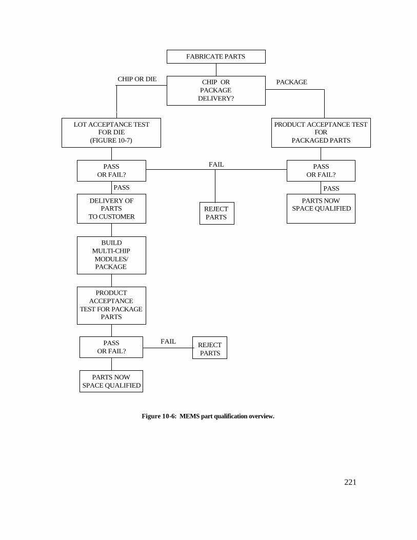
221
CHIP OR DIE PACKAGE
REJECT PARTS
FAIL
PASSPASS
REJECT PARTS
FAIL
PARTS NOWSPACE QUALIFIED
PASSOR FAIL?
PRODUCTACCEPTANCE
TEST FOR PACKAGEPARTS
BUILDMULTI-CHIPMODULES/PACKAGE
DELIVERY OFPARTS
TO CUSTOMER
PASSOR FAIL?
LOT ACCEPTANCE TESTFOR DIE
(FIGURE 10-7)
PARTS NOWSPACE QUALIFIED
PASSOR FAIL?
PRODUCT ACCEPTANCE TESTFOR
PACKAGED PARTS
CHIP ORPACKAGE
DELIVERY?
FABRICATE PARTS
Figure 10-6: MEMS part qualification overview.
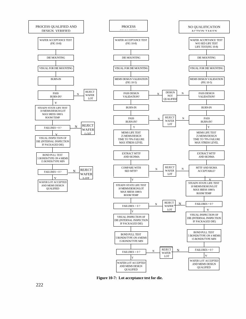
222
REJECTWAFER LOT
REJECTWAFER LOT
N
N N
YY
REJECTWAFER LOT
N N
Y
Y
Y
REJECTWAFER LOT
N
REJECTWAFER LOT
N
DESIGNNOT
QUALIFIED
N NPASSBURN-IN?
BURN-IN
VISUAL FOR DIE MOUNTING
DIE MOUNTING
WAFER ACCEPTANCE TEST(FIG 10-8)
WAFER LOT ACCEPTEDAND MEMS DESIGN
QUALIFIED
FAILURES = 0 ?
BOND PULL TEST5 BONDS/TYPE ON 4 MEMS
15 BONDS/TYPE MIN
VISUAL INSPECTION OFDIE (INTERNAL INSPECTION
IF PACKAGED DIE)
FAILURES = 0 ?
STEADY-STATE LIFE TEST10 MEMS/DESIGN/LOT
MAX SRESS 1000 hROOM TEMP
COMPARE WITHSED MTTF?
EXTRACT MTTFAND SIGNMA
MEMS LIFE TEST25 MEMS/DESIGN
TIME TO 70% FAILUREMAX STRESS LEVEL
PASSBURN-IN?
BURN-IN
PASS DESIGNVALIDATION?
MEMS DESIGN VALIDATION(FIG 10-5)
VISUAL FOR DIE MOUNTING
DIE MOUNTING
WAFER ACCEPTANCE TEST(FIG 10-8)
MTTF AND SIGMAACCEPTABLE?
EXTRACT MTTFAND SIGNMA
MEMS LIFE TEST25 MEMS/DESIGN
TIME TO 70% FAILUREMAX STRESS LEVEL
PASSBURN-IN?
BURN-IN
PASS DESIGNVALIDATION?
MEMS DESIGN VALIDATION(FIG 10-5)
VISUAL FOR DIE MOUNTING
DIE MOUNTING
WAFER ACCPETANCE TESTW/O SED LIFE TESTLIFE TEST(FIG 10-8)
WAFER LOT ACCEPTEDAND MEMS DESIGN
QUALIFIED
FAILURES = 0 ?
BOND PULL TEST5 BONDS/TYPE ON 4 MEMS
15 BONDS/TYPE MIN
VISUAL INSPECTION OFDIE (INTERNAL INSPECTION
IF PACKAGED DIE)
FAILURES = 0 ?
STEADY-STATE LIFE TEST10 MEMS/DESIGN/LOT
MAX SRESS 1000 hROOM TEMP
WAFER LOT ACCEPTEDAND MEMS DESIGN
QUALIFIED
FAILURES = 0 ?
BOND PULL TEST5 BONDS/TYPE ON 4 MEMS
15 BONDS/TYPE MIN
VISUAL INSPECTION OFDIE (INTERNAL INSPECTION
IF PACKAGED DIE)
FAILURES = 0 ?
STEADY-STATE LIFE TEST10 MEMS/DESIGN/LOT
MAX SRESS 1000 hROOM TEMP
Y
Y
Y
Y
Y
Y
REJECTWAFER
LOT
N
REJECTWAFER
LOT
N
N
N
PROCESS QUALIFIED ANDDESIGN VERIFIED
PROCESSQUALIFIED
NO QUALIFICATIONACTION TAKEN
Figure 10-7: Lot acceptance test for die.
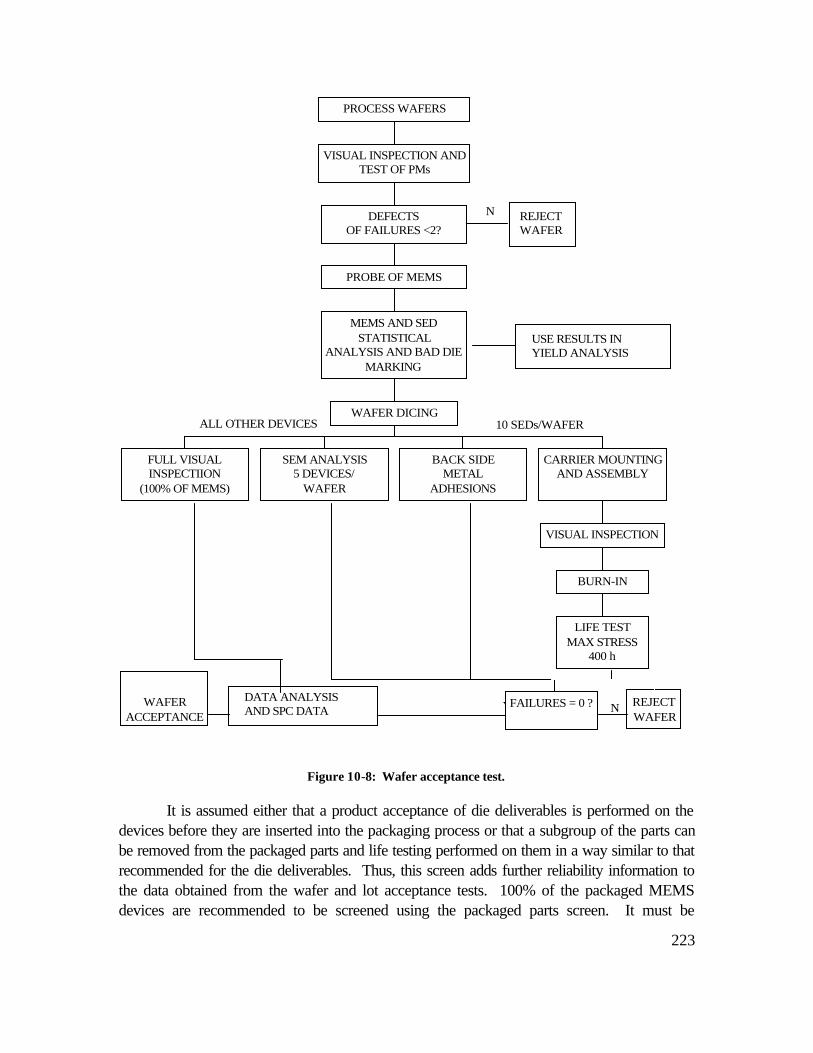
223
N
10 SEDs/WAFERALL OTHER DEVICES
DATA ANALYSISAND SPC DATA
WAFERACCEPTANCE
Y
N REJECTWAFER
USE RESULTS INYIELD ANALYSIS
N
FULL VISUALINSPECTIION
(100% OF MEMS)
SEM ANALYSIS5 DEVICES/
WAFER
BACK SIDEMETAL
ADHESIONS
FAILURES = 0 ? REJECTWAFER
LIFE TESTMAX STRESS
400 h
BURN-IN
VISUAL INSPECTION
CARRIER MOUNTINGAND ASSEMBLY
WAFER DICING
MEMS AND SED STATISTICAL
ANALYSIS AND BAD DIEMARKING
PROBE OF MEMS
DEFECTSOF FAILURES <2?
VISUAL INSPECTION ANDTEST OF PMs
PROCESS WAFERS
Figure 10-8: Wafer acceptance test.
It is assumed either that a product acceptance of die deliverables is performed on thedevices before they are inserted into the packaging process or that a subgroup of the parts canbe removed from the packaged parts and life testing performed on them in a way similar to thatrecommended for the die deliverables. Thus, this screen adds further reliability information tothe data obtained from the wafer and lot acceptance tests. 100% of the packaged MEMSdevices are recommended to be screened using the packaged parts screen. It must be

224
understood that this is only a recommended screen and not all tests will be necessary for alldevices.
Table 10-1 shows the recommended screening tests that can be used for MEMSpackaged devices and the reference for the screen. This information is modified from MIL-PRF-38534 Class K requirements and should be applied after careful consideration of theapplicability and mission requirements. It should be kept in mind that these tests are designedfor microelectronic circuits and may need to be modified for specific applications of MEMS.
Test Reference
Nondestructive bond pull MIL-STD-883, Method 2023Internal visual inspection MIL-STD-883, Method 2017IR-scan (prior to seal)1 JEDEC Document JES2 [39]Mechanical Shock MIL-STD-883, Method 2002Constant Acceleration MIL-STD-883, Method 2001Temperature cycling MIL-STD-883, Method 1010Thermal shock MIL-STD-883, Method 1011Particle impact noise detection MIL-STD-883, Method 2020Electrical Customer’s specificationsBurn-in MIL-STD-883, Method 1015Electrical (high/low) temp Customer’s specificationsFine leakGross leak
MIL-STD-883, Method 1014MIL-STD-883, Method 1014
Radiographic MIL-STD-883, Method 2012External visual MIL-STD-883, Method 2009
Table 10-1: Typical packaged device screening.
Throughout the rest of this chapter, a brief description of, and the rationale for, eachproduct acceptance test or screen will be given.
A. SEM Analysis
Scanning Electron Microscopy analysis can provide valuable information regarding thestep coverage and quality of the metallization and passivation on device. Thus, this tool isrequired as part of the wafer acceptance tests. Some accept/reject criteria are provided inMIL-STD-883, but they may need some modification to cover different MEMS technologies.
1 This test may only be necessary if a MEMS device has on-chip electronics.
225
B. Nondestructive Bond Pull Test
The integrity of wire bonds cannot always be judged through visual and electrical tests.Therefore, some qualification procedures recommend the implementation of a nondestructivebond pull test of each bond. The pull force selected for this test is generally dependent on thematerial and wire diameter in question. MIL-STD-883, Method 2023, is normally used for thisapplication. Obviously selecting the required pull force is critical and must be decided by themanufacturer and the user.
Mechanical damage to good bonds as a result of the test is possible. Due to thisproblem, some manufacturers have removed this step from their qualification and screenprocedures and resorted to in-process controls and testing to provide the necessary information.The decision to require this test must be made by the MEMS user after careful consideration ofthe system application and workmanship of the manufacturer.
C. Visual Inspection
Many defects in MEMS, such as substrate cracks, poor wire bonds, and foreignmaterials, reduce device reliability. Cracks can separate devices that are designed to bemechanically coupled, thus changing the mechanical characteristics of the device. Poor wirebonds increase the resistivity of the device, which can change the anticipated electrical output.Conductive particulates can short out devices, causing huge current flow through tiny fingers ofcomb drives. To prevent these and any other obvious flaws from impinging upon deviceperformance, a visual screen of a device is performed during wafer acceptance tests for defectsof the die and during the packaged device screens for packaging and bonding defects.
D. Laser Profile
Since some MEMS will have unacceptably high residual stresses, it is useful to measurethe warping in a device caused by these stresses. One method of doing this is to use a laserprofiling system to examine surface contour. These systems record non-planar displacementsthrough the use of laser interferometry and have proven useful in the analysis of MEMS. Onelimitation to these systems is that they do not distinguish between surface contour and internalstress. The only tactic that has proven effective for differentiating between these two effects isto use differential measuring of surface profiles on devices that are etched on both sides. Fordevices suspended above the substrate, there is no method available for directly measuringinternal stress.
E. IR Scan
Some defects, such as substrate cracks and die-attach voids, must be detected, whetheror not they are visible. Since these types of defects have a different thermal conductivity than
226
the surrounding defect free region, they may be detected through thermal mapping. The baselinefor comparison is the thermal profile of the MEMS device that was made as part of the productor design verification step. Typically a 5 oC variation in thermal output is enough for a device tobe considered a reject. However, this step may not prove that informative if the temperature ofthe MEMS device does not vary much from the ambient temperature. Thus the applicability ofthis test will be design dependent and will likely require enough on-chip electronics to noticeablyheat the device.
Although infrared microscopes are expensive, require calibration, and have a minimumresolution of approximately 15 µm, they are the best method of mapping a device’s thermalcharacteristics, since they do not damage the device. While this screening step is not typicallyimposed as a requirement following MIL-PRF-38534, it is a good idea for any high powerapplications or application, such as those involving thermal actuators, that require good thermalstability. This step should be performed after die attach and before attachment of the packagelid.
F. Mechanical Shock Screen
This screen is intended to detect weak parts that are required to undergo severe shocksduring transportation, handling, satellite launch, or other operations. The test subjects thepackaged MEMS to a number of short shock pulses with a defined peak. Failures are detectedduring final visual and electrical screens.
G. Constant Acceleration
This screen is intended to detect failures due to mechanical weaknesses by subjectingthe packaged MEMS to a constant acceleration. Typical failures occur in the bonds and dieattach, and these are detected during the final visual and electrical screens. This screen is aneffective tool to detect poor workmanship. The appendix to this section describes methods forproducing mission specific dynamic tests for MEMS and can be used either as a supplement ora replacement for the military standards.
H. Temperature Cycling and Shock Screen
Failure in mechanical devices can be accelerated by applying thermal stress. These testsdetect structural defects or weak points in packaging that would normally result in early failures.Temperature cycling consists of cycling a packaged MEMS between extreme temperaturesmany times. Typically the temperatures used are –65 to 200 oC and the number of cycles is 15.The temperature shock screen is similar to the temperature cycle screen in that the test involvessubjecting the packaged MEMS to extreme low and high temperature, usually -65 to 150 oC,over many cycles. The difference is that the rate of change in temperature with respect to time ismuch greater. Temperature shock screens are typically done between baths of hot and cold
227
materials, while cycling screens use conductive air cooling to change temperature. Failuredetection for both screens is done in a final electrical and visual inspection. These tests are alsodiscussed in great detail in MIL-STD-883, Methods 1010 and 1011.
I. Particle Impact Noise Detection
During encapsulation, thermal stress screens, and mechanical tests, particles may breakoff from either the MEMS device or the package. These loose particles may mechanicallydamage the MEMS or short out part of the circuit. That particle impact noise detection screen,or PIND, is a nondestructive test used to find parts that have this defect. During the test, thepart is vibrated and a sensor is used to detect anomalous noise. Failure criteria are given inMIL-STD-883, Method 2020.
J. Burn-In
In an ideal world, devices that were substandard would be eliminated by a wellcontrolled process line before they ever reach the customer. However, it is unrealistic toassume that a manufacturer can detect or predict which devices will fail with 100% accuracy.Therefore, to eliminate the device discussed in Chapter 2 as being part of the infant mortalitygroup in a given production population, the burn-in screen must be performed.
The burn-in screen stresses devices above their normal operating conditions toaccelerate any early failure that would occur from latent defects. For electronic circuits, burn-inis typically done at elevated temperatures to accelerate early failure mechanisms. For MEMS,the import of elevated temperatures will be device dependent. Far more likely to be of use isthe practice of supplying a voltage that is above the normal operating regime for a device.
The difficulty in the burn-in test is to select a level of testing that will weed out weakdevices while not damaging good ones. An implicit trade off in burn-in is that the confidencethat a device will not suffer infant mortality comes at the expense of its long-term life expectancy.Thus, running the test for too long can be as problematic as running it in an abbreviated manner.The exact details of the burn-in will be up to the manufacturer and customer to decide in tryingto balance the two conflicting goals of confidence and lifetime with the mission requirements.Devices that fail burn-in, which is usually defined as a pre-determined shift in outputcharacteristics, should be discarded, rather than have any attempts made to salvage them.
K. Leak Test
There was a fair amount of information devoted to the subject of contamination andinduced failure mechanisms in Chapter 3. To eliminate many of these problems, many MEMSdevices are hermetically sealed in their packages and for these devices, their reliability is
228
dependent upon the integrity of these seals. The thermal and mechanical tests were intended todetect defects in packaging but often a leak test is required to find failed devices.
Fine leak tests consist of placing the packaged device in a chamber pressurized with aknown gas, which will enter the package through any cracks that have developed. Usuallyhelium or nitrogen gas with a small concentration of a radioactive isotope is used, since thesegases can be detected in small concentrations using commercially available equipment. After atime, the chamber is cleansed by circulating air and the packages are tested to determine if gasleaks from them. Although the use of radioactive isotopes sounds somewhat extreme, it is thepreferred method in high-volume production lines due to the fact that it is easier to detect for alonger period of time. The disadvantage of this method is that the gas will escape from a grossleak before it has time to be detected. Therefore, a gross leak test is used that is similar to thefine leak test except that it is conducted with a pressurized liquid bath instead of the gas.
L. Radiographic
The final screen is usually a radiographic picture of the inside of the sealed packagetaken with an x-ray machine. This nondestructive test uses radiation to penetrate the packagewalls and produce a shadow image on a photographic plate. It is useful for checking thelocation and position of wire bonds and for detecting loose particles that may have moved orbroken off during the screening process. In some cases, this screen can also be useful indetermining the presence of die-attach voids.
IV. Company Certification
Procurement of MEMS will often be the result of long-term partnerships between thecustomer and manufacturer in which both parties collaborate in order to assure the reliability andperformance specifications of the flight ready device. This close relationship between the twoparties evolves through mutual trust. In a new partnership, the best way for a manufacturer toestablish trust is to show that it has good control over the facilities, processes, and personnelused to make these devices. Typically these controls, which include documentation,procedures, and management practices, are part of a Quality Management Program. This stepof proving that the company has these processes in place is referred to as “companycertification” and is usually verified by the MEMS user through a written or facility audit. It isrecommended that the audit and company certification be completed before the contract for adeliverable MEMS device is signed. In some cases, the MEMS user may make thisrequirement a paramount consideration in selecting a company from which to buy parts. Acompany that does not have tight quality controls installed should not be allowed to supplyMEMS for high-rel applications.
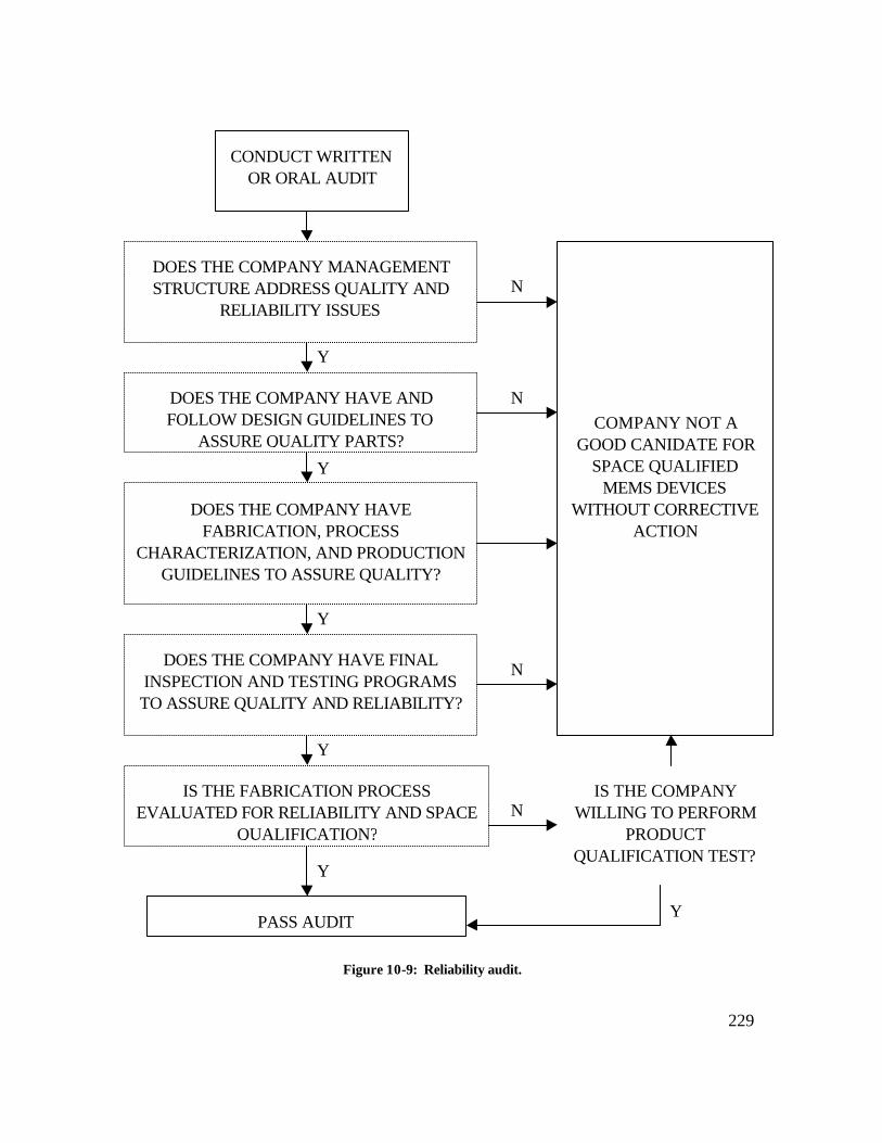
229
CONDUCT WRITTENOR ORAL AUDIT
DOES THE COMPANY MANAGEMENTSTRUCTURE ADDRESS QUALITY AND
RELIABILITY ISSUES
DOES THE COMPANY HAVE ANDFOLLOW DESIGN GUIDELINES TO
ASSURE QUALITY PARTS?
DOES THE COMPANY HAVEFABRICATION, PROCESS
CHARACTERIZATION, AND PRODUCTIONGUIDELINES TO ASSURE QUALITY?
DOES THE COMPANY HAVE FINALINSPECTION AND TESTING PROGRAMSTO ASSURE QUALITY AND RELIABILITY?
IS THE FABRICATION PROCESSEVALUATED FOR RELIABILITY AND SPACE
QUALIFICATION?
COMPANY NOT AGOOD CANIDATE FOR
SPACE QUALIFIEDMEMS DEVICES
WITHOUT CORRECTIVEACTION
PASS AUDIT
IS THE COMPANYWILLING TO PERFORM
PRODUCTQUALIFICATION TEST?
Y
Y
Y
Y
Y
Y
N
N
N
N
Figure 10-9: Reliability audit.
230
Since most of the information sought during company certification is based uponestablished quality control programs and standard industry methodologies,[1] the audit shouldbe easy and inexpensive for both the user and manufacturer. Manufacturers should keep thisinformation available and ready for distribution at all times. This whole process may befacilitated if the manufacturer has passed previous qualification audits, in which case this stepmay only require an update from previous audits.
A simplified version of the audit is shown in Figure 10-9. The audit for a specificMEMS must be developed on a case-by-case basis. The major items in the QualityManagement Program are presented in the rest of this section, but it must be remembered thatthis is only a partial list. As stated before, the end goal of a reliable MEMS device is ultimatelyin the hands of the user. Any additional device specific tests must be specified by the user asneeded.
A. Technology Review Board
In order to assure the quality and reliability of MEMS, manufacturers will usually have apermanent committee in place with authoritative knowledge of the entire fabrication process. Ifthe quality of the process is not maintained, this committee, called the Technology ReviewBoard, or TRB for short, will have power to change the process to improve quality. The TRBis responsible for the following measures:
• The development, implementation, and documentation of the manufacturer’s QualityManagement Program and Quality Management Plan.
• The development, implementation, and documentation of the manufacturer’s ProcessQualification, Product Qualification, and Product Acceptance Plans.
• Compiling and maintaining all records of the fabrication process, statistical process control(SPC) procedures, SPC data, certification and qualification processes, reliability dataanalysis, and corrective actions taken to remedy reliability problems.
• Examining test structures and MEMS reliability data and establishing and implementingcorrective actions when the reliability of the devices decreases.
• Notifying customers when the reliability of a wafer lot is questioned and supplying thecustomers an evaluation of the problem and any corrective action required.
• Supplying reliability data to customers.
Because of these great responsibilities that cover such a broad area of knowledge, themembers of the TRB should have good hands-on knowledge of device design, technologydevelopment, wafer fabrication, assembly, testing, and quality assurance procedures. While the
231
members of the TRB board are usually from the manufacturing company, it is not unusual for acustomer to request a seat on the board for their products.
B. Conversion of Customer Requirements
Not all customers express their specifications in the same way, and not all MEMSmanufacturers publish their performance specifications and operating guidelines in the same way.Normally a user will ask for a device with specific characteristics, such as an accelerometer witha dynamic range of +/- 50g and a resolution of .1g instead of saying that they want a bulkmicromachined device with a cantilever beam accelerometer. It is the job of the manufacturer touse the requirements of the user to determine the device design. It is through the conversion ofthe customer’s specifications to the manufacturer’s designs that the manufacturer can determinethe cost and reliability concerns of the device. It is recommended that the procedure by which acustomer’s requirements are converted to the manufacturer’s working instructions bedocumented. A typical document will describe the procedure a company performs, the order inwhich they are performed, and the typical schedule. Some of the items typically included in thisconversion are:
• Relating customer device requirements to manufacturer device requirements.
• Converting the device requirements to a device design, using controlled design proceduresand tools (i.e. established electric, geometric, mechanical, and reliability design rules).
• Establishing a design review team.
• Selection of test structures.
• Mask generation procedure within the controlled design procedure.
• Wafer-fabrication-capabilities baseline.
• Circuit fabrication procedure in accordance with approved design, mask, fabrication,assembly, and test flows.
• Incoming inspection and supplier procurement document covering design, mask, fabrication,and assembly.
• Establishment of screening and traveler documents.
• Technology Conformance Inspection, or TCI, procedures.
• Marking requirements.
232
• Rework procedures.
C. Manufacturing Control Procedures
MEMS manufacture is a complicated process that involves multiple materials and steps,each of which are critical to final device performance and reliability. Only a properly controlledmanufacturing line can be expected to routinely produce quality MEMS devices. For thisreason, the customer needs to be assured that the manufacturer is using only certified processesand qualified technologies at every step of the manufacturing process. To obtain that level ofassurance, the company certification audit should review the manufacturer’s procedure for:
• Traceability of all materials and products to the wafer lot.
• Incoming inspection to assure conformance to the material specification.
• Electrostatic discharge, or ESD, control in handling the material in all stages ofmanufacturing.
• Conformance with design requirements at:
1. Device procurement specification
2. Layout verification
3. Testability and fault coverage verification
4. Electrical and mechanical parameter performance extraction
5. Archived data
• Conformance with fabrication requirements at:
1. Mask fabrication
2. Mask inspection
3. Wafer fabrication
• Assembly and package requirements.
• Electrical and mechanical testing.
Most of this information can be obtained by examining the manufacturer’s process flow.
D. Equipment Calibration and Maintenance
In order to maintain device quality, the processing equipment must be maintained. Forthis reason, all equipment used in the manufacturing process must be kept to the equipment
233
manufacturer’s specifications. In addition to routine maintenance, the equipment must also becalibrated on a regular basis. Documentation showing the maintenance and calibration schedule,departures from this schedule, and corrective action taken due to these departures should bekept by the manufacturers. This documentation will also highlight any major discrepancies foundin the calibration and maintenance of a piece of equipment, since it could affect the reliability ofthe MEMS. The TRB will review this documentation to determine if any corrective action isrequired. Further information on equipment calibration can be found in Reference [31].
E. Training Programs
Even well maintained and calibrated equipment cannot produce quality devices withoutskilled operators. To assure the skills of the personnel employed in the design, fabrication, andtesting of devices, each engineer, scientist, and technician should have formal training relative totheir tasks. Furthermore, retesting and retraining should be provided regularly to maintain theworker’s proficiency, especially if new equipment or procedures are introduced into themanufacturing process. It is therefore recommended that the work training and testing practicesemployed to establish, evaluate, and maintain the skills of personnel engaged in reliability-criticalwork be documented with respect to form, content, and frequency.
F. Corrective Action Program
One of the best ways to continuously improve the reliability of manufactured parts is totest and analyze failed parts from all stages of manufacturing and, based on these findings, makecorrective actions to the manufacturing process or to the education of the end users. The planthat describes these corrective actions is normally documented and should detail the specificsteps followed by the manufacturer to correct any process that is found to be defective. Thedocumentation should also include the mechanisms and time frames involved in informingcustomers of potential reliability problems.
G. Self-Audit Program
To promote continual quality improvement, manufacturers regularly review theirmanufacturing procedures through an independent internal self-audit program under the directionof the TRB. The self-audit program should identify the critical review areas, their frequency ofaudit, and the corrective action system to be employed when deviations from requirements arefound. Typical areas included in a self-audit are:
• Calibration and preventive maintenance,
• Fabrication procedures,
• Training programs,
• Electrical and mechanical tests,

234
• Failure analysis programs,
• Test methods,
• Environmental control,
• Incoming inspection,
• Inventory control and traceability,
• Statistical Process Control and
• Record Retention.
The self-audit checklist, the date of the previous audits, and all the findings from theaudits are typically maintained by the TRB, which will use these findings to recommendcorrective actions and prepare a self-audit follow-up.
H. Electrostatic Discharge Handling Program
Because of the catastrophic failure caused by ESD, all personnel that work with MEMSshould be trained in the proper procedures for handling the devices. Furthermore, theseprocedures should be documented and available for reference. Typically, the proceduresinclude the methods, equipment, and materials used in the handling, packaging and testing ofMEMS. Further guidance for device handling is available in the Electronics IndustryAssociation JEDEC Publication EIA 625 [33] and MIL-STD-1686.[34]
I. Cleanliness and Atmospheric Controls
The quality of MEMS and the yield of the fabrication line is directly linked to themanufacturer’s control over the cleanliness of the environment in which the parts are fabricated.Therefore, manufacturers often spend a large amount of their resources to guarantee thatdevices are fabricated in ultraclean rooms where the atmosphere is tightly controlled. Since theyield of the fabrication process is so strongly dependent on the success of maintaining thoseconditions, regular measurements are taken to assure the temperature, humidity, and cleanlinessof the fabrication areas. In addition, during transit and storage prior to seal, the die/wafer shouldbe protected from human contact, machine overspray, or other sources of contamination. All ofthese procedures and measurements are recorded and compiled into a single document by theclean-room manager for future reference.
J. Record Retention
Documentation is the only method available to gauge the reliability of MEMS as a functionof time, which is critical to spotting faults in the process line. Although many sections in thisguide recommend the documentation of certain data or procedures, it is helpful if a list of

235
documents and the period of retention for each document is made. Furthermore, the list shouldcontain a record of when each document was last changed, who is responsible for maintainingthe document, and where the document is stored. The typical documents to be retained arethose that relate to
• Inspection operations,
• Failure and defect report and analysis,
• Initial documentation and subsequent changes in design, materials, or processing,
• Equipment calibration,
• Process, utility, and material controls,
• Product lot identification,
• Product traceability,
• Self-audit report,
• Personnel training and testing and
• TRB meeting minutes.
K. Inventory Control
The proper inventory of all incoming materials and outgoing parts is not only required forthe management of a profitable company but also for the manufacture of reliable MEMSdevices. Many materials and chemicals used in the fabrication of MEMS have shelf lives thatmust be tracked if process yield and reliability are to be maintained. The tracking of in-processand completed MEMS is essential for the establishment of MEMS history, which is critical infailure analysis. Therefore, the methods and procedures used to control the inventory of allmaterials related to MEMS manufacturing should be documented. This documentation typicallyincludes:
• Incoming inspection requirements and reports.
• Identification and segregation of non-conforming materials.
• Identification and control of limited-life materials.
• Control of raw materials.
• Data retention for required receiving reports, test reports, certification, etc.
236
• Supplier certification plan.
L. Statistical Process Control
The establishment of a statistical baseline for judging the continuous improvement of amanufacturer’s process is an important task. To establish that baseline, the manufacturer shoulddevelop an SPC program using in-process monitoring techniques to control the key processingsteps that affect device yield and reliability. As part of the SPC process, every wafer lottypically has built-in control monitors from which data are gathered, which should then beanalyzed by appropriated SPC methods to determine the effectiveness of the company’scontinuous improvement plans. Additional information on SPC analysis can be found in theElectronics Industry Association JEDEC EIA 556A [35] and in MIL-I-38535.[36]
V. Additional Reading
Microelectronics Failure Analysis Techniques, A Procedural Guide, E. Doyle, Jr., and B.Morris, Editors, report written for Air Force Systems Command, Rome Air DevelopmentCenter under contracts F30602-78-C-0339 and F30602-78-C-0281
MIL-STD-1540C, Test Requirements for Launch, Upper-Stage and Space Vehicles,United States Air Force Military Standard, 1994.
Thomson, W. T., “Theory of Vibration with Applications,” 2nd ed., Prentice-Hall, Inc.,Engelwood Cliffs, New Jersey, 1981.
Kinsler, L. E. and A. R. Frey, “Fundamentals of Acoustics,” 2nd ed., John Wiley & Sons, Inc.,New York, 1962.
Markstein, H. W., “Designing Electronics for High Vibration and Shock,” ElectronicPackaging & Production, April 1987, pp. 40-43.
MIL-STD-462, Electromagnetic Emission and Susceptibility, Test Methods for, UnitedStates Department of Defense Military Standard.
237
Appendix: Mission Specific Environmental Testing
J. Newell and K. Man
One of the challenges in space qualification is to define the operational environment of apart such that it is tested to the limits of a mission without requiring expensive overdesign. Toaid this, this section defines, discusses and recommends environmental design and verificationrequirements for space microelectromechanical systems. Typical environmental programpolicies are presented, along with environmental design and test configuration requirements.Sample specifications are provided for a variety of environments, ranging from launch vehicledynamics to ground handling conditions. Through judicious implementation of the analysis, testand verification techniques outlined herein, robust and reliable MEMS devices can bedeveloped for long term survival in the unforgiving space environment.
A. Test Procedures
The fundamental purposes of an environmental test program are to simulate the launchenvironment, to qualify designs for launch and in-service conditions, and to screen flighthardware for manufacturing workmanship. Such a program should effectively demonstrate thequality and reliability of a design, as well as its suitability for the intended purpose or mission.
Environmental Compatibility Analyses are often conducted to verify hardware designcompliance with mission environments that are impractical to verify by test. Design margins forthese analyses must normally be higher than margins demonstrated by environmental test.
Such analyses are often conducted for the ground handling environment, includingvibration and shock, temperature and humidity. Analyses are also normally conducted todemonstrate compatibility with explosive atmosphere requirements, and to prove structuralintegrity under launch pressure decay and thermal shock conditions.
Environmental Testing is conducted at two levels: the assembly/subsystem level and thesystem level. Assembly/subsystem level testing is completed prior to delivery for higher levelintegration into a flight system, and is generally the responsibility of a cognizant hardwareengineer. The majority of space micromechanisms fall into this category. Post deliveryenvironmental testing at a higher level of system integration is then usually conducted under theauspices of an Assembly, Test and Launch Operations, or ATLO, Manager.
Environmental tests are categorized for the purpose of hardware quality and reliabilityverification as Protoflight, Qualification and Acceptance, which are defined as follows.
238
Protoflight tests are conducted on flight hardware to demonstrate its ability to meetmission requirements. Protoflight test levels are generally equal to qualification levels, althoughtest duration is often reduced.
Qualification tests are performed to a level and/or duration sufficient to demonstrateability of a hardware design to meet mission requirements, with adequate margin. Such testing isgenerally conducted on a dedicated unit.
Acceptance tests are performed to detect workmanship or other defects which mayhave been introduced in the fabrication process, and to demonstrate hardware acceptability forflight. Acceptance testing is performed on flight hardware and spares when an adequateprotoflight or qualification heritage exists.
In addition, development environmental testing is also often conducted to gain insightinto design compatibility or functionality in expected mission environments. As an example, adynamics test model of a flight system is sometimes assembled for purposes of structuralverification.
i) Test Sequencing
To accurately simulate the environment sequence, flight hardware testing should beperformed as follows:
1. Sinusoidal or transient vibration, random vibration, pyroshock and acoustics,as required. The order among these dynamics tests may be interchanged.
2. Thermal-vacuum testing.
During the normal flight sequence, the launch environment is followed by vacuum andpotential temperature extremes. In this flight sequence, hardware is exposed to acoustics andvibration followed by vacuum and temperature variations. Consequently, by performingdynamics tests prior to thermal-vacuum tests, the actual flight sequence will be simulated. If theflight sequence produces synergistic effects, the synergism will also be simulated.
Experience has shown that until the thermal-vacuum tests are performed, many failuresinduced during dynamics testing are not detected because of the short duration of the dynamicstests. In addition, the thermal-vacuum test on flight hardware at both the assembly level and thesystem level provides a good screen for intermittent as well as incipient hardware failures.
Preserving the sequence of service environments in the environmental test program is awidely accepted practice. As a result, the effect of reversing the test sequence on spacecraftfailure rates has not been quantified. However, evidence exists that many acoustic inducedfailures have not been detected until the spacecraft is exposed to the thermal-vacuum
239
environment. These failures may not be detected during acoustics tests because of the shortone-minute duration or a non-operating power condition. Typically, the identified failures thatcould be related to or caused by the dynamic acoustic environment were bad solder joints,intermittents, bad bearings, broken wires, poor welds, leaks, and foreign materials.
An example of a failure that might be induced by dynamic tests but not revealed untilthermal vacuum, would be a broken wire or solder joint. This defect might be induced byacoustics but not be detected during the acoustic test due to the short duration of the test or toan unpowered or unmonitored state of the affected equipment. During post-acoustic functionaltesting, the wire or solder joint broken ends may be making adequate contact to show electricalcontinuity. In the subsequent thermal-vacuum test, the thermal distortions could cause loss ofcontact, allowing the failure to be detected. Reversing the test sequence could result in thedefect not being induced until after thermal vacuum test and not detected until exposure to theflight thermal environment.
Even if all defects precipitated by the dynamics tests are revealed during the test orduring post-test functional testing, performing dynamic tests first will nonetheless increase theprobability of early defect detection, when correction of defects will have less impact on theflight program cost and schedule.
If the thermal-vacuum tests do not follow the dynamics tests, more intermittent orincipient discontinuity type failures may go undetected. If the defects are not detected duringassembly level tests and are subsequently detected during the system level tests, redesign orrework at this late stage of the process could cause delays, increase costs, or make it necessaryto accept additional risk that might have been avoided. If the defects are not detected at thesystem level, the defects may then cause hardware anomalies during the mission, and in theextreme could cause a mission failure.
B. Environmental Test Requirements
Appropriate in-situ environments must be determined and specified in order to effect arobust space microelectromechanical device design. These environmental design requirementsdepend upon factors ranging from the choice of launch vehicle to the type of spacecraft thermalcontrol subsystem. Establishment of these requirements can be a time consuming task involvingconsiderable research and analysis effort.
The requirements within this section encompass the basic launch environments, as wellas those associated with ground operations and handling. They are offered here as genericbaseline environmental levels, and should be used primarily as examples.
240
i) Launch Environment
The launch environment encompasses pre-launch operations, liftoff, and ascent. Typicalrequirements are provided here for both design and test of space micro- electromechanicaldevices, with environments including thermal conditions, deep space vacuum and insertionpressure decay, random and sinusoidal vibration, pyrotechnic shock and acoustic noise.
ii) Thermal
Spacecraft microelectromechanical systems should be designed to operate withinspecification over the temperature range of -55°C to +70°C, or flight allowable ±20°C,whichever is more extreme.
iii) Definitions
Terms used in thermal design and test of space microelectromechanical systems aredefined as follows:
Operating Allowable Flight Temperatures: The temperature ranges of MEMS deviceswhen powered-on in a worst case operational mode (hot or cold). In-spec operation isrequired.
Non-Operating Allowable Flight Temperatures: The temperature ranges of MEMS deviceswhen powered-off in a worst case non-operational mode (hot or cold). MEMS devices mustbe capable of returning to in-spec operation as temperatures return to Operating AllowableFlight levels.
Design Temperature Limits: Temperature limits to which all MEMS devices should bedesigned to meet all functional and performance specifications.
Stabilization Temperature: In specification of test conditions, an assembly is defined to haveattained a stabilization temperature when the rate of temperature change of its largest centrallylocated thermal mass is less than 2°C per hour.
Control Temperature - Conductive Heat Transfer Tests: The control temperature for athermal/vacuum conductive heat transfer test is defined to be the temperature of the heatexchanger plate midway between input and output of heat exchange fluid.
Control Temperature - Radiative Heat Transfer Tests: The control temperature for athermal/vacuum radiative heat transfer test is defined to be the temperature of the major
241
temperature control surface of the assembly (e.g. radiator).
iv) Thermal Radiation
Assembly allowable flight temperatures should not be exceeded during the missionunder exposure to the applicable worst case expected thermal radiation levels in theaccompanying table.
Mission Phase Direct Solar Reflected Solar
(Albedo)
Planetary IR
(LW Radiation)
Earth Orbit: 0 to 1400 W/m2
(5770K effective
blackbody temperature)
0 to 0.32
0 to 450 W/m2
(global annual mean)
0 to 0.70 W/m2
(polar regions)
100 to 270 W/m2
(206K to 262K effective
blackbody
temperature)
Deep Space Cruise:
Near Earth 0 to 1400 W/m2
(at earth
perihelion)
Negligible beyond 4 earth
radii
Negligible beyond 4
earth radii
Table A-1: Thermal radiation levels.
v) Vacuum Pressure Decay
The design pressure for a typical mission can be expected to decrease from 101325N/m2 (760 Torr) on Earth to 1.33 x 10⁻³ N/m2 (1x10⁻⁵ Torr) in deep space. A typical launchpressure decay rate, showing launch vehicle internal fairing pressure versus time, is provided inthe figure below.
242
0
1
2
3
4
5
6
7
8
9
10
11
12
13
14
15
0 5 10 15 20 25 30 35 40 45 50 55 60 65 70
Time (seconds)
Maximum Pressure
Minimum Pressure
Figure A-1: Launch pressure decay rate.
Assemblies affected by launch pressure decay should be designed with a recommendedstructural design factor of 1.0 on yield and 1.4 on ultimate if tested, or 1.6 on yield and 2.0 onultimate if not tested.
vi) Dynamics
Assembly-level vibration and shock tests, simulating launch vibroacoustics and upper-stage pyrotechnic separation events, represent the most severe dynamic environments forspacecraft hardware. Components of a spacecraft, at various levels of assembly, shouldgenerally be subjected to the following environments:
(1) Definitions
Sinusoidal vibration requirements are imposed to cover the various mid-frequency (5-100 Hz)launch vehicle-induced transient loading events.
Random vibration requirements are derived from launch vehicle induced acoustic excitationsduring liftoff, transonic and maximum dynamic pressure (e.g. “max q”) events.
Acoustic requirements are based on maximum internal payload fairing sound pressure levelspectra.
243
Pyroshock requirements are intended to represent the structurally transmitted transients fromexplosive separation devices, including pyrotechnic fasteners utilized to effect spacecraftseparation from the upper stage.
Quasi-Static Accelerations are associated with quasi-steady flight events generated by rocketmotor-induced forces and other external forces which change slowly with time and for which theelastic responses are relatively small. Typical assembly design requirements for quasi-staticacceleration environments are specified in the table below.
Axis Acceleration (g)ThrustLateral
+14 ± 0.7+3 ± 0.3
Table A-2: Quasi-static accelerations.
Qualification testing of microelectromechanical systems for the quasi-static accelerationenvironment can be performed in a centrifuge. However, a low frequency sine vibration test,conducted on an electrodynamic shaker, can often be substituted for the relatively expensivecentrifuge trial. If a microelectromechanical system is subjected to sine testing at a frequencysufficiently below its fundamental resonance, it will not vibrate, but will instead move as a rigidbody under the input sine acceleration. To ensure pure rigid body behavior of the assemblyunder test, the frequency of sine excitation should generally be less than themicroelectromechanical system resonance by a factor of two. More detail on each of the othertest environments is provided below.
(2) Dynamics Test Tolerances
Tolerances for dynamics testing are provided below. The indicated tolerances arederived from space vehicle hardware test experience, and may be facility-, equipment-, andpersonnel-dependent.
a. Time: +5 percent
b. Vibration Frequency: +5 percent or 1 Hz, whichever is greater.
c. Acoustic Spectral Shape: Match to spectral shape of the specified SoundPressure Level (SPL) in 1/3 octave bands.
d. Acoustic Overall Level: + 1 dB of the specified level.
e. Random Vibration Spectral Shape: The Acceleration Spectral Density(ASD) shall be within +3 dB when measured in frequency bands no widerthan 25 Hz.
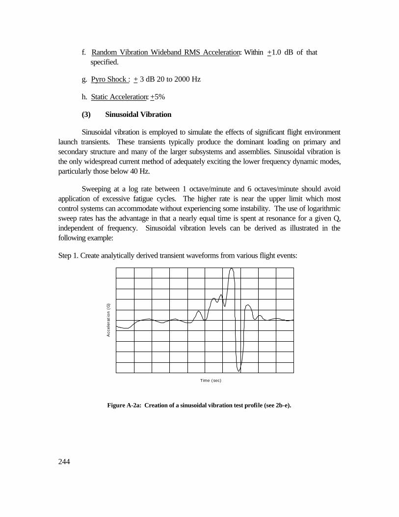
244
f. Random Vibration Wideband RMS Acceleration: Within +1.0 dB of thatspecified.
g. Pyro Shock : + 3 dB 20 to 2000 Hz
h. Static Acceleration: +5%
(3) Sinusoidal Vibration
Sinusoidal vibration is employed to simulate the effects of significant flight environmentlaunch transients. These transients typically produce the dominant loading on primary andsecondary structure and many of the larger subsystems and assemblies. Sinusoidal vibration isthe only widespread current method of adequately exciting the lower frequency dynamic modes,particularly those below 40 Hz.
Sweeping at a log rate between 1 octave/minute and 6 octaves/minute should avoidapplication of excessive fatigue cycles. The higher rate is near the upper limit which mostcontrol systems can accommodate without experiencing some instability. The use of logarithmicsweep rates has the advantage in that a nearly equal time is spent at resonance for a given Q,independent of frequency. Sinusoidal vibration levels can be derived as illustrated in thefollowing example:
Step 1. Create analytically derived transient waveforms from various flight events:
Acc
eler
atio
n (G
)
Time (sec)
Figure A-2a: Creation of a sinusoidal vibration test profile (see 2b-e).
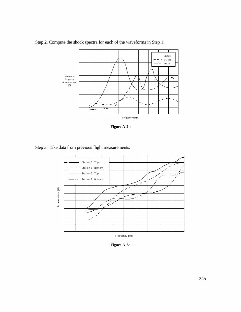
245
Step 2. Compute the shock spectra for each of the waveforms in Step 1:
Frequency (Hz)
MaximumResponse
Acceleration(G)
Launch
SRB Sep
MECO
Figure A-2b
Step 3. Take data from previous flight measurements:
Station 1, Top
Station 1, Bottom
Station 2, Top
Station 2, Bottom
Frequency (Hz)
Acc
eler
atio
n (G
)
Figure A-2c
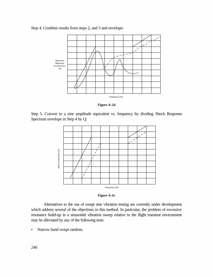
246
Step 4. Combine results from steps 2, and 3 and envelope:
Frequency (Hz)
MaximumResponse
Acceleration(G)
Figure A-2d
Step 5. Convert to a sine amplitude equivalent vs. frequency by dividing Shock ResponseSpectrum envelope in Step 4 by Q:
Frequency (Hz)
Peak
Acc
eler
atio
n (G
)
Figure A-2e
Alternatives to the use of swept sine vibration testing are currently under developmentwhich address several of the objections to this method. In particular, the problem of excessiveresonance build-up in a sinusoidal vibration sweep relative to the flight transient environmentmay be alleviated by any of the following tests:
• Narrow band swept random.
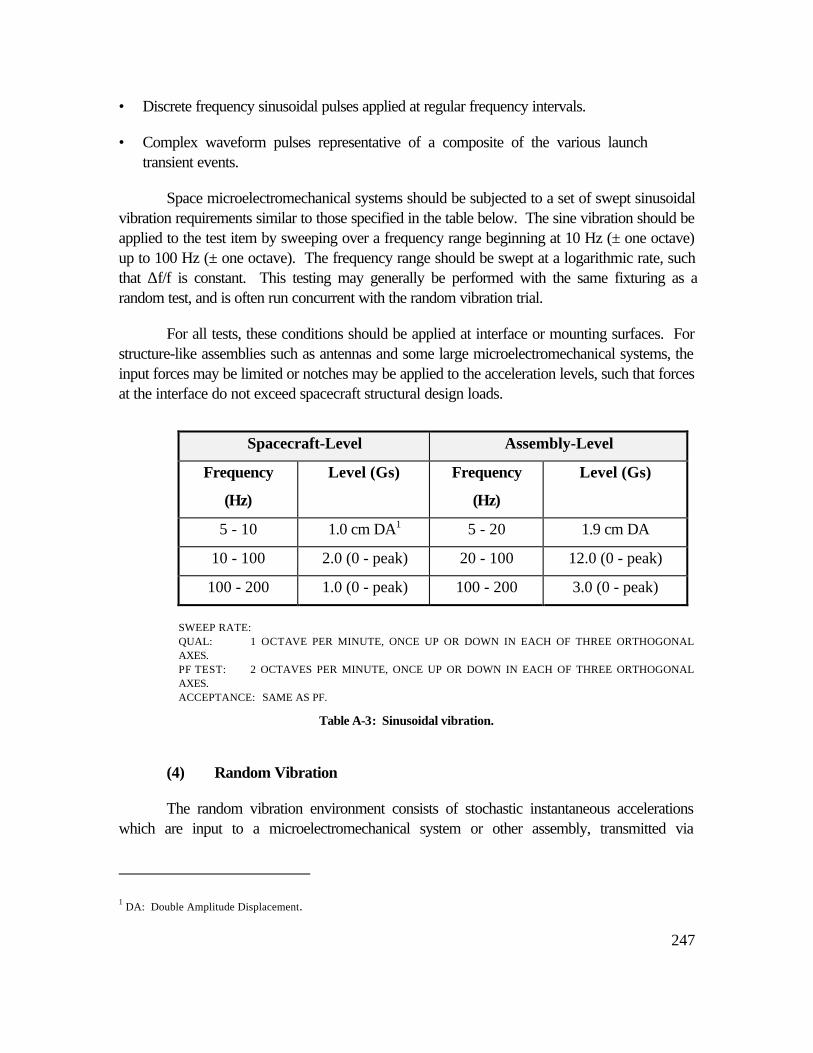
247
• Discrete frequency sinusoidal pulses applied at regular frequency intervals.
• Complex waveform pulses representative of a composite of the various launchtransient events.
Space microelectromechanical systems should be subjected to a set of swept sinusoidalvibration requirements similar to those specified in the table below. The sine vibration should beapplied to the test item by sweeping over a frequency range beginning at 10 Hz (± one octave)up to 100 Hz (± one octave). The frequency range should be swept at a logarithmic rate, suchthat ∆f/f is constant. This testing may generally be performed with the same fixturing as arandom test, and is often run concurrent with the random vibration trial.
For all tests, these conditions should be applied at interface or mounting surfaces. Forstructure-like assemblies such as antennas and some large microelectromechanical systems, theinput forces may be limited or notches may be applied to the acceleration levels, such that forcesat the interface do not exceed spacecraft structural design loads.
Spacecraft-Level Assembly-Level
Frequency
(Hz)
Level (Gs) Frequency
(Hz)
Level (Gs)
5 - 10 1.0 cm DA1 5 - 20 1.9 cm DA
10 - 100 2.0 (0 - peak) 20 - 100 12.0 (0 - peak)
100 - 200 1.0 (0 - peak) 100 - 200 3.0 (0 - peak)
SWEEP RATE:QUAL: 1 OCTAVE PER MINUTE, ONCE UP OR DOWN IN EACH OF THREE ORTHOGONALAXES.PF TEST: 2 OCTAVES PER MINUTE, ONCE UP OR DOWN IN EACH OF THREE ORTHOGONALAXES.ACCEPTANCE: SAME AS PF.
Table A-3: Sinusoidal vibration.
(4) Random Vibration
The random vibration environment consists of stochastic instantaneous accelerationswhich are input to a microelectromechanical system or other assembly, transmitted via
1 DA: Double Amplitude Displacement.
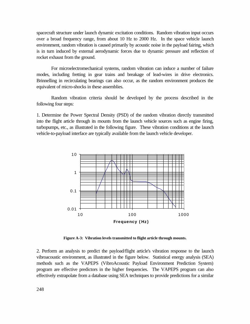
248
spacecraft structure under launch dynamic excitation conditions. Random vibration input occursover a broad frequency range, from about 10 Hz to 2000 Hz. In the space vehicle launchenvironment, random vibration is caused primarily by acoustic noise in the payload fairing, whichis in turn induced by external aerodynamic forces due to dynamic pressure and reflection ofrocket exhaust from the ground.
For microelectromechanical systems, random vibration can induce a number of failuremodes, including fretting in gear trains and breakage of lead-wires in drive electronics.Brinnelling in recirculating bearings can also occur, as the random environment produces theequivalent of micro-shocks in these assemblies.
Random vibration criteria should be developed by the process described in thefollowing four steps:
1. Determine the Power Spectral Density (PSD) of the random vibration directly transmittedinto the flight article through its mounts from the launch vehicle sources such as engine firing,turbopumps, etc., as illustrated in the following figure. These vibration conditions at the launchvehicle-to-payload interface are typically available from the launch vehicle developer.
0.01
0.1
1
10
10 100 1000
Frequency (Hz)
Figure A-3: Vibration levels transmitted to flight article through mounts.
2. Perform an analysis to predict the payload/flight article's vibration response to the launchvibroacoustic environment, as illustrated in the figure below. Statistical energy analysis (SEA)methods such as the VAPEPS (VibroAcoustic Payload Environment Prediction System)program are effective predictors in the higher frequencies. The VAPEPS program can alsoeffectively extrapolate from a database using SEA techniques to provide predictions for a similar
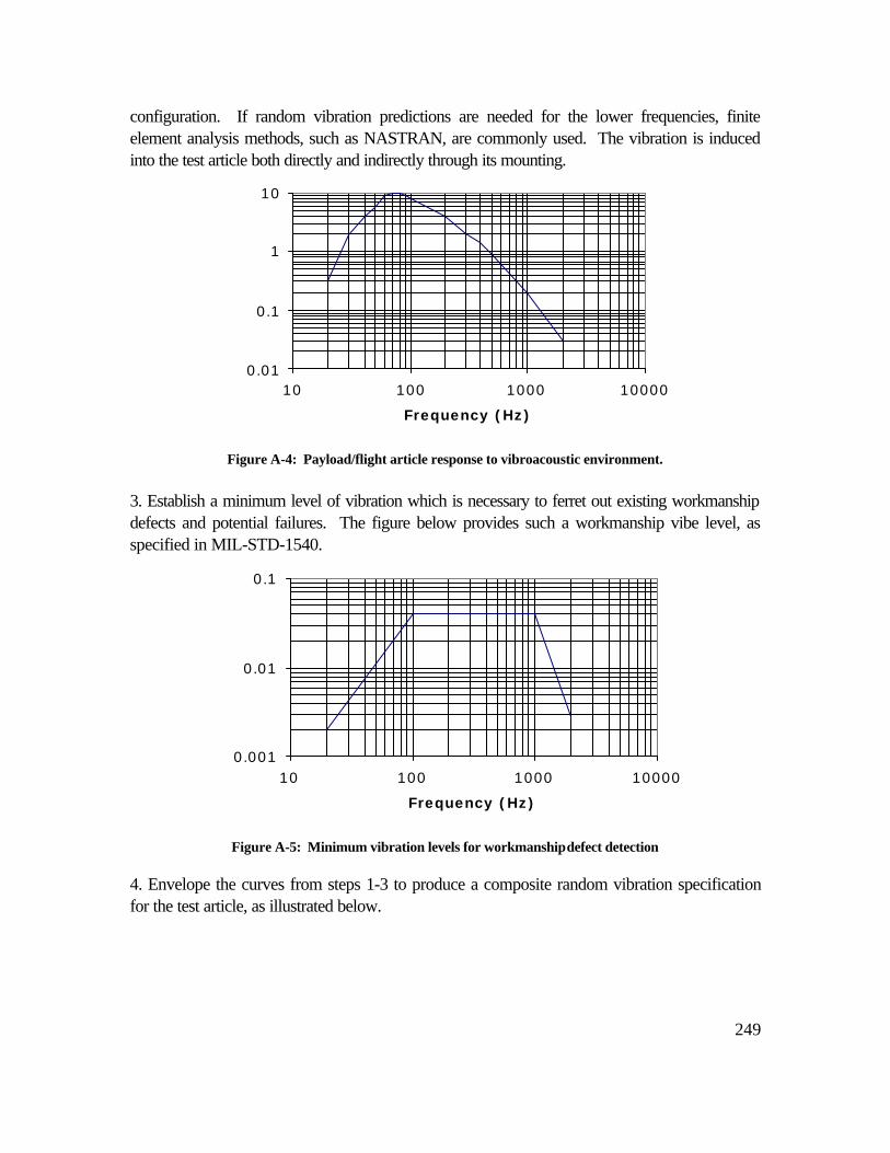
249
configuration. If random vibration predictions are needed for the lower frequencies, finiteelement analysis methods, such as NASTRAN, are commonly used. The vibration is inducedinto the test article both directly and indirectly through its mounting.
0.01
0.1
1
10
10 100 1000 10000
Frequency (Hz)
Figure A-4: Payload/flight article response to vibroacoustic environment.
3. Establish a minimum level of vibration which is necessary to ferret out existing workmanshipdefects and potential failures. The figure below provides such a workmanship vibe level, asspecified in MIL-STD-1540.
0.001
0.01
0.1
10 100 1000 10000
Frequency (Hz)
Figure A-5: Minimum vibration levels for workmanship defect detection
4. Envelope the curves from steps 1-3 to produce a composite random vibration specificationfor the test article, as illustrated below.

250
0.001
0.01
0.1
1
10
1 10 100 1000 10000
Frequency (Hz)
Envelope
Figure A-6: Composite random vibration envelope.
This resultant random vibration specification, which is employed as the flight acceptancetest level, covers the two primary sources of this vibration while also providing an effectiveprocess for uncovering workmanship defects. Qualification and Protoflight test levels areincreased typically 3 to 6 dB above flight acceptance to verify that the design is not marginal.
Recommended random vibration environments for both spacecraft and assembly-leveltesting are specified in the accompanying table. Instantaneous accelerations are assumed toexhibit a gaussian distribution. For structure-like assemblies such as antennas and some largeinstruments, force limit criteria should be used in testing to mitigate the problem of impedancemismatch between the test article and rigid shaker fixture.
Typically, microelectromechanical systems and similar assemblies are mounted tospacecraft structure which is somewhat flexible. If, during a launch event, the MEMS is excitedinto a state of mechanical resonance, the relatively low stiffness spacecraft mount will serve tolimit interface forces. On the other hand, if a microelectromechanical system resonates during avibration test, the interface forces between shaker and test article can become artificially high, asthe infinite impedance shaker continues to drive the resonating mechanical structure to thespecification acceleration power spectral density level. To mitigate this problem, the inputvibration specification can be notched at resonances or force limiting can be effected. Eitherway, the interface forces will be limited to more realistic levels, and an unnecessary overtest willbe avoided.
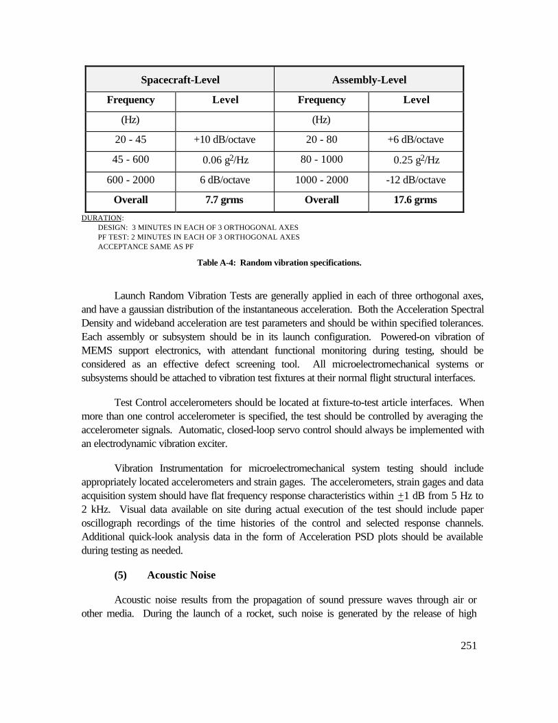
251
Spacecraft-Level Assembly-Level
Frequency Level Frequency Level
(Hz) (Hz)
20 - 45 +10 dB/octave 20 - 80 +6 dB/octave
45 - 600 0.06 g2/Hz 80 - 1000 0.25 g2/Hz
600 - 2000 6 dB/octave 1000 - 2000 -12 dB/octave
Overall 7.7 grms Overall 17.6 grms
DURATION: DESIGN: 3 MINUTES IN EACH OF 3 ORTHOGONAL AXES PF TEST: 2 MINUTES IN EACH OF 3 ORTHOGONAL AXES ACCEPTANCE SAME AS PF
Table A-4: Random vibration specifications.
Launch Random Vibration Tests are generally applied in each of three orthogonal axes,and have a gaussian distribution of the instantaneous acceleration. Both the Acceleration SpectralDensity and wideband acceleration are test parameters and should be within specified tolerances.Each assembly or subsystem should be in its launch configuration. Powered-on vibration ofMEMS support electronics, with attendant functional monitoring during testing, should beconsidered as an effective defect screening tool. All microelectromechanical systems orsubsystems should be attached to vibration test fixtures at their normal flight structural interfaces.
Test Control accelerometers should be located at fixture-to-test article interfaces. Whenmore than one control accelerometer is specified, the test should be controlled by averaging theaccelerometer signals. Automatic, closed-loop servo control should always be implemented withan electrodynamic vibration exciter.
Vibration Instrumentation for microelectromechanical system testing should includeappropriately located accelerometers and strain gages. The accelerometers, strain gages and dataacquisition system should have flat frequency response characteristics within +1 dB from 5 Hz to2 kHz. Visual data available on site during actual execution of the test should include paperoscillograph recordings of the time histories of the control and selected response channels.Additional quick-look analysis data in the form of Acceleration PSD plots should be availableduring testing as needed.
(5) Acoustic Noise
Acoustic noise results from the propagation of sound pressure waves through air orother media. During the launch of a rocket, such noise is generated by the release of high
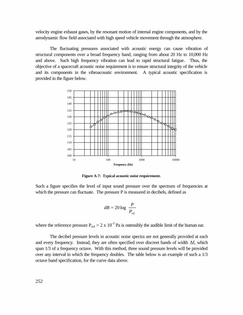
252
velocity engine exhaust gases, by the resonant motion of internal engine components, and by theaerodynamic flow field associated with high speed vehicle movement through the atmosphere.
The fluctuating pressures associated with acoustic energy can cause vibration ofstructural components over a broad frequency band, ranging from about 20 Hz to 10,000 Hzand above. Such high frequency vibration can lead to rapid structural fatigue. Thus, theobjective of a spacecraft acoustic noise requirement is to ensure structural integrity of the vehicleand its components in the vibroacoustic environment. A typical acoustic specification isprovided in the figure below.
Such a figure specifies the level of input sound pressure over the spectrum of frequencies atwhich the pressure can fluctuate. The pressure P is measured in decibels, defined as
=
refPP
dB log20
where the reference pressure Pref = 2 x 10⁻⁵ Pa is ostensibly the audible limit of the human ear.
The decibel pressure levels in acoustic noise spectra are not generally provided at eachand every frequency. Instead, they are often specified over discreet bands of width ∆f, whichspan 1/3 of a frequency octave. With this method, three sound pressure levels will be providedover any interval in which the frequency doubles. The table below is an example of such a 1/3octave band specification, for the curve data above.
100
105
110
115
120
125
130
135
140
145
150
10 100 1000 10000
Frequency (Hz)
Figure A-7: Typical acoustic noise requirement.
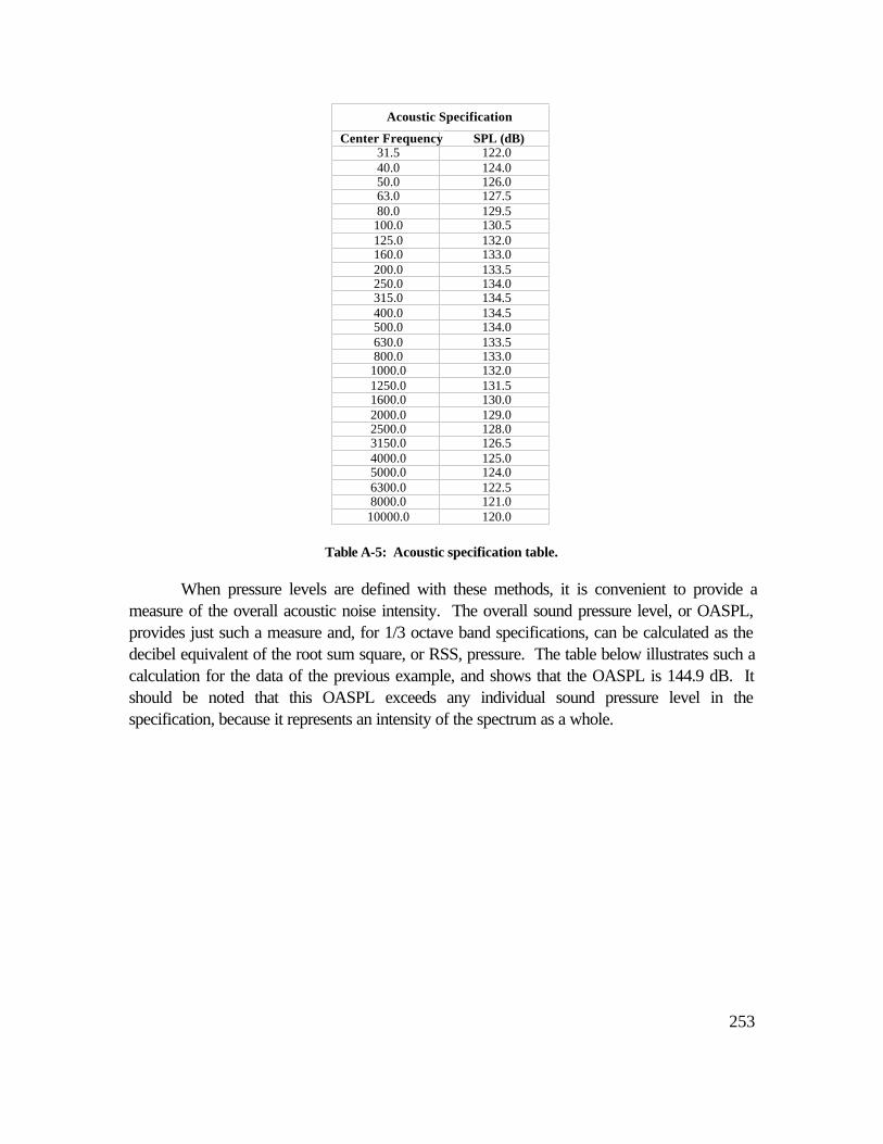
253
Acoustic Specification
Center Frequency SPL (dB)31.5 122.040.0 124.050.0 126.063.0 127.580.0 129.5
100.0 130.5125.0 132.0160.0 133.0200.0 133.5250.0 134.0315.0 134.5400.0 134.5500.0 134.0630.0 133.5800.0 133.0
1000.0 132.01250.0 131.51600.0 130.02000.0 129.02500.0 128.03150.0 126.54000.0 125.05000.0 124.06300.0 122.58000.0 121.0
10000.0 120.0
Table A-5: Acoustic specification table.
When pressure levels are defined with these methods, it is convenient to provide ameasure of the overall acoustic noise intensity. The overall sound pressure level, or OASPL,provides just such a measure and, for 1/3 octave band specifications, can be calculated as thedecibel equivalent of the root sum square, or RSS, pressure. The table below illustrates such acalculation for the data of the previous example, and shows that the OASPL is 144.9 dB. Itshould be noted that this OASPL exceeds any individual sound pressure level in thespecification, because it represents an intensity of the spectrum as a whole.
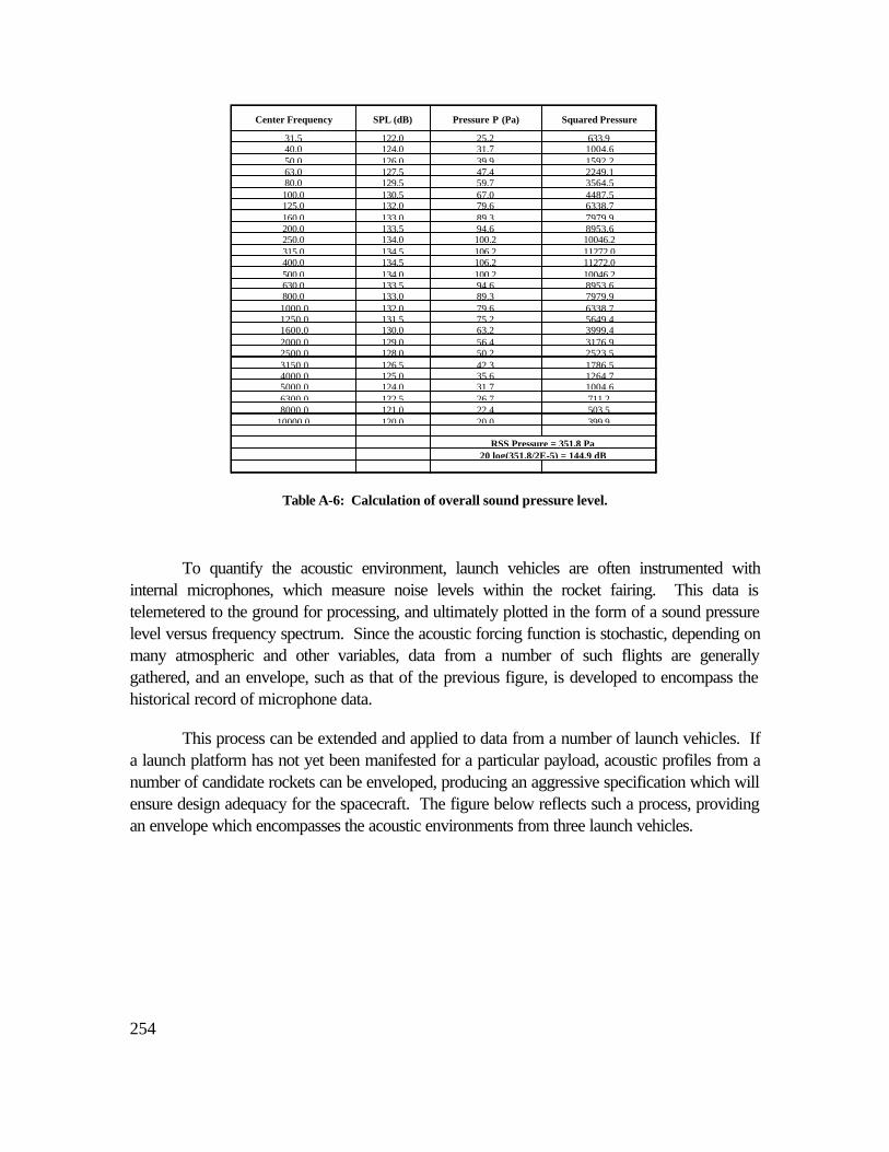
254
Center Frequency SPL (dB) Pressure P (Pa) Squared Pressure
31.5 122.0 25.2 633.940.0 124.0 31.7 1004.650.0 126.0 39.9 1592.263.0 127.5 47.4 2249.180.0 129.5 59.7 3564.5100.0 130.5 67.0 4487.5125.0 132.0 79.6 6338.7160.0 133.0 89.3 7979.9200.0 133.5 94.6 8953.6250.0 134.0 100.2 10046.2315.0 134.5 106.2 11272.0400.0 134.5 106.2 11272.0500.0 134.0 100.2 10046.2630.0 133.5 94.6 8953.6800.0 133.0 89.3 7979.91000.0 132.0 79.6 6338.71250.0 131.5 75.2 5649.41600.0 130.0 63.2 3999.42000.0 129.0 56.4 3176.92500.0 128.0 50.2 2523.53150.0 126.5 42.3 1786.54000.0 125.0 35.6 1264.75000.0 124.0 31.7 1004.66300.0 122.5 26.7 711.28000.0 121.0 22.4 503.5
10000.0 120.0 20.0 399.9
RSS Pressure = 351.8 Pa20 log(351.8/2E-5) = 144.9 dB
Table A-6: Calculation of overall sound pressure level.
To quantify the acoustic environment, launch vehicles are often instrumented withinternal microphones, which measure noise levels within the rocket fairing. This data istelemetered to the ground for processing, and ultimately plotted in the form of a sound pressurelevel versus frequency spectrum. Since the acoustic forcing function is stochastic, depending onmany atmospheric and other variables, data from a number of such flights are generallygathered, and an envelope, such as that of the previous figure, is developed to encompass thehistorical record of microphone data.
This process can be extended and applied to data from a number of launch vehicles. Ifa launch platform has not yet been manifested for a particular payload, acoustic profiles from anumber of candidate rockets can be enveloped, producing an aggressive specification which willensure design adequacy for the spacecraft. The figure below reflects such a process, providingan envelope which encompasses the acoustic environments from three launch vehicles.
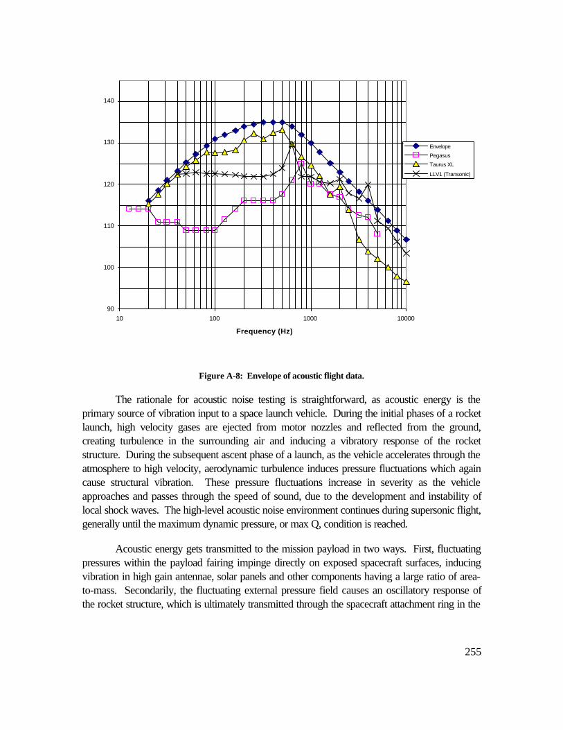
255
90
100
110
120
130
140
10 100 1000 10000
Frequency (Hz)
Envelope
Pegasus
Taurus XL
LLV1 (Transonic)
Figure A-8: Envelope of acoustic flight data.
The rationale for acoustic noise testing is straightforward, as acoustic energy is theprimary source of vibration input to a space launch vehicle. During the initial phases of a rocketlaunch, high velocity gases are ejected from motor nozzles and reflected from the ground,creating turbulence in the surrounding air and inducing a vibratory response of the rocketstructure. During the subsequent ascent phase of a launch, as the vehicle accelerates through theatmosphere to high velocity, aerodynamic turbulence induces pressure fluctuations which againcause structural vibration. These pressure fluctuations increase in severity as the vehicleapproaches and passes through the speed of sound, due to the development and instability oflocal shock waves. The high-level acoustic noise environment continues during supersonic flight,generally until the maximum dynamic pressure, or max Q, condition is reached.
Acoustic energy gets transmitted to the mission payload in two ways. First, fluctuatingpressures within the payload fairing impinge directly on exposed spacecraft surfaces, inducingvibration in high gain antennae, solar panels and other components having a large ratio of area-to-mass. Secondarily, the fluctuating external pressure field causes an oscillatory response ofthe rocket structure, which is ultimately transmitted through the spacecraft attachment ring in the
256
form of random vibration. From the spacecraft perspective, this random input is generallylowest at the launch vehicle attachment plane, and increases upward along the payload axis.
At the integrated spacecraft level acoustic noise is a primary source of vibrationexcitation. It should be included in virtually any space vehicle test program. At the subsystemlevel, however, and particularly in the context of space MEMS, acoustic testing is generally notconducted due to the obvious low ratio of area-to-mass exhibited by a microelectromechanicalsystem.
The failure modes produced by acoustic noise excitation are generally identical to thoseassociated with other types of vibratory structural fatigue. These include failures due toexcessive displacement, in which one deflecting component makes contact with another, as wellas fractured structural members and loose fasteners. Broken solder joints, cracked PC boardsand wave guides can also occur. Electronic components whose function depends on the motionof structural parts, such as relays and pressure switches, are particularly susceptible.
Large flat panels are most easily influenced by, and therefore damaged by, acousticenergy, as they can undergo large displacements while oscillating at low frequency. For atypical spacecraft, this means that a fixed high gain antenna must be carefully designed andstiffened to avoid bending failures, debonding of composite members and related problems. Ingeneral, any structure with a high ratio of surface area to mass can be expected to experiencepotential problems in the acoustic noise environment.
Supporting data for acoustic noise design, analysis and testing can be found in theliterature, as well as in various launch vehicle user manuals. The acoustic test has traditionallybeen severe, with the qualification environment generally established at 4 dB above the expectedlaunch noise profile. The table below provides a sampling of problems detected during acoustictests on several large programs.

257
Acoustic Test Problem/Failure History
Program Year Subsystem Failure Mode
Viking 1973 S/X Band Antenna Cracked Epoxy
Viking 1973 S/X Band Antenna Spacers Loosened
Viking 1973 S/X Band Antenna Studs Loosened
Viking 1973 Infrared Mapper Wire Shorted
Viking 1973 Radio Antenna Screw Sheared
Voyager 1977 S/X Band Antenna Magnetic Coil Debonded
Galileo 1983 Dust Detector Sensor Cover Buckled
Mars Observer 1991 Telecom Subsystem HGA Screws Backed Out
Mars Observer 1991 High Gain Antenna HGA Struts Debonded
Mars Observer 1991 High Gain Antenna Waveguide Broke
Topex 1992 Instrument Module I/C Lead Wire Broke
Cassini 1995 High Gain Antenna HGA Screws Backed Out
Cassini 1995 High Gain Antenna HGA Struts Debonded
Table A-7: Acoustic test problem/failure history.
The testing has clearly identified improperly designed components. It is interesting tonote that a majority of these problems have occurred in high gain antennas and relatedsubsystems, which have the previously identified characteristics of large surface areas, low massand bonded attachments.
Failure mode sensitivities and cost tradeoffs for the acoustic noise environment areillustrated in the table below. The primary test variables are acoustic noise input level, timeduration for the test, frequency of noise input and whether or not power is on in the test article.
Each test parameter in an acoustic noise trial is generally a cost driver. This is primarilydue to the fact that the test requires a large chamber, many support personnel and a significantamount of equipment.
Requ i r emen t C o n t r o l P a r a m e t e r s Fa i l u r e Modes S e n s i t i v i t y t o I n c r e a s e C o s td B tdur p o w e r f
Acoustic Noise dB peak intermittents + + + + dB increase = more N2, etc. +t duration broken solder joints + + 0 - t duration change +power on opens + + 0 + power on = extra equipt +frequency shorts + + 0 + f increase = better modulator +
broken connectors + + 0 -broken wave guides + + 0 -broken crystals + + 0 +cracked diodes + + 0 +relay chatter + + + +fastener loosening + + 0 +potentiometer slippage + + 0 +
Table A-8: Control parameter sensitivity and cost.
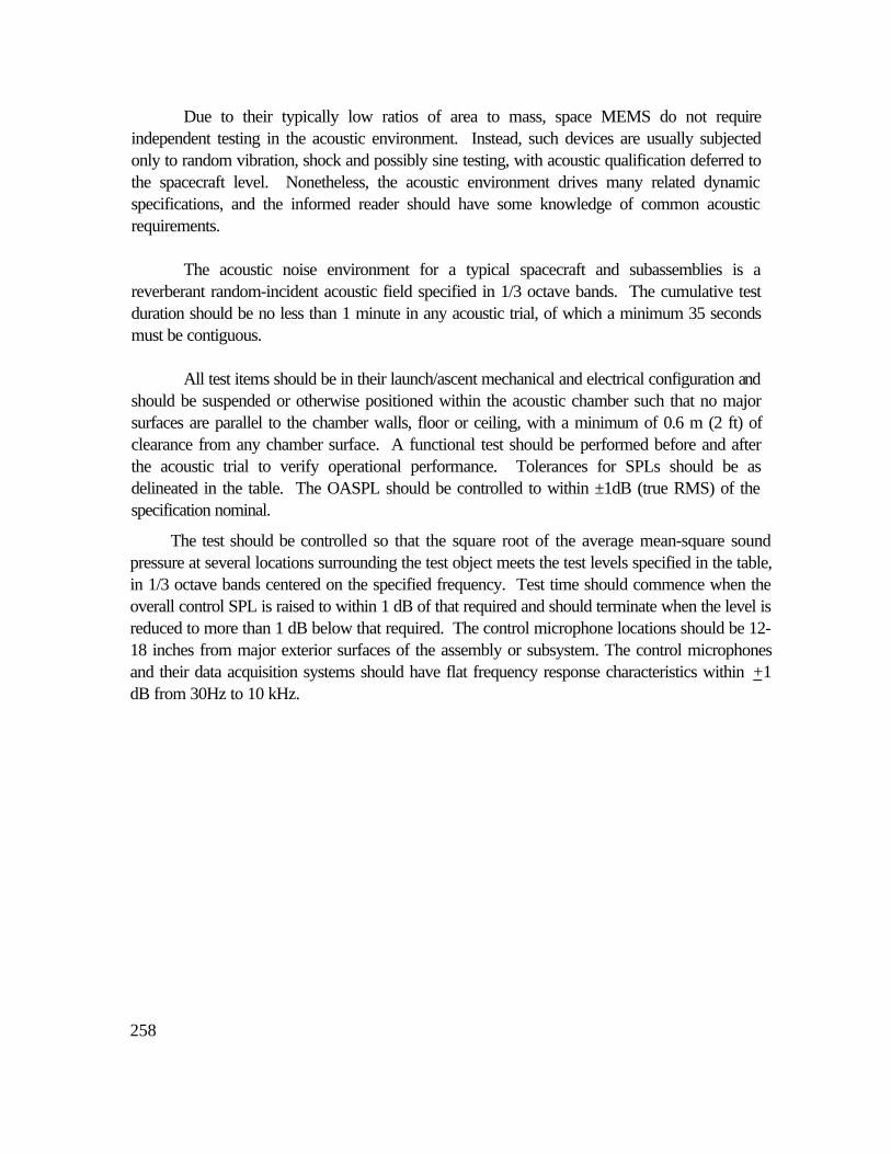
258
Due to their typically low ratios of area to mass, space MEMS do not requireindependent testing in the acoustic environment. Instead, such devices are usually subjectedonly to random vibration, shock and possibly sine testing, with acoustic qualification deferred tothe spacecraft level. Nonetheless, the acoustic environment drives many related dynamicspecifications, and the informed reader should have some knowledge of common acousticrequirements.
The acoustic noise environment for a typical spacecraft and subassemblies is areverberant random-incident acoustic field specified in 1/3 octave bands. The cumulative testduration should be no less than 1 minute in any acoustic trial, of which a minimum 35 secondsmust be contiguous.
All test items should be in their launch/ascent mechanical and electrical configuration andshould be suspended or otherwise positioned within the acoustic chamber such that no majorsurfaces are parallel to the chamber walls, floor or ceiling, with a minimum of 0.6 m (2 ft) ofclearance from any chamber surface. A functional test should be performed before and afterthe acoustic trial to verify operational performance. Tolerances for SPLs should be asdelineated in the table. The OASPL should be controlled to within ±1dB (true RMS) of thespecification nominal.
The test should be controlled so that the square root of the average mean-square soundpressure at several locations surrounding the test object meets the test levels specified in the table,in 1/3 octave bands centered on the specified frequency. Test time should commence when theoverall control SPL is raised to within 1 dB of that required and should terminate when the level isreduced to more than 1 dB below that required. The control microphone locations should be 12-18 inches from major exterior surfaces of the assembly or subsystem. The control microphonesand their data acquisition systems should have flat frequency response characteristics within +1dB from 30Hz to 10 kHz.
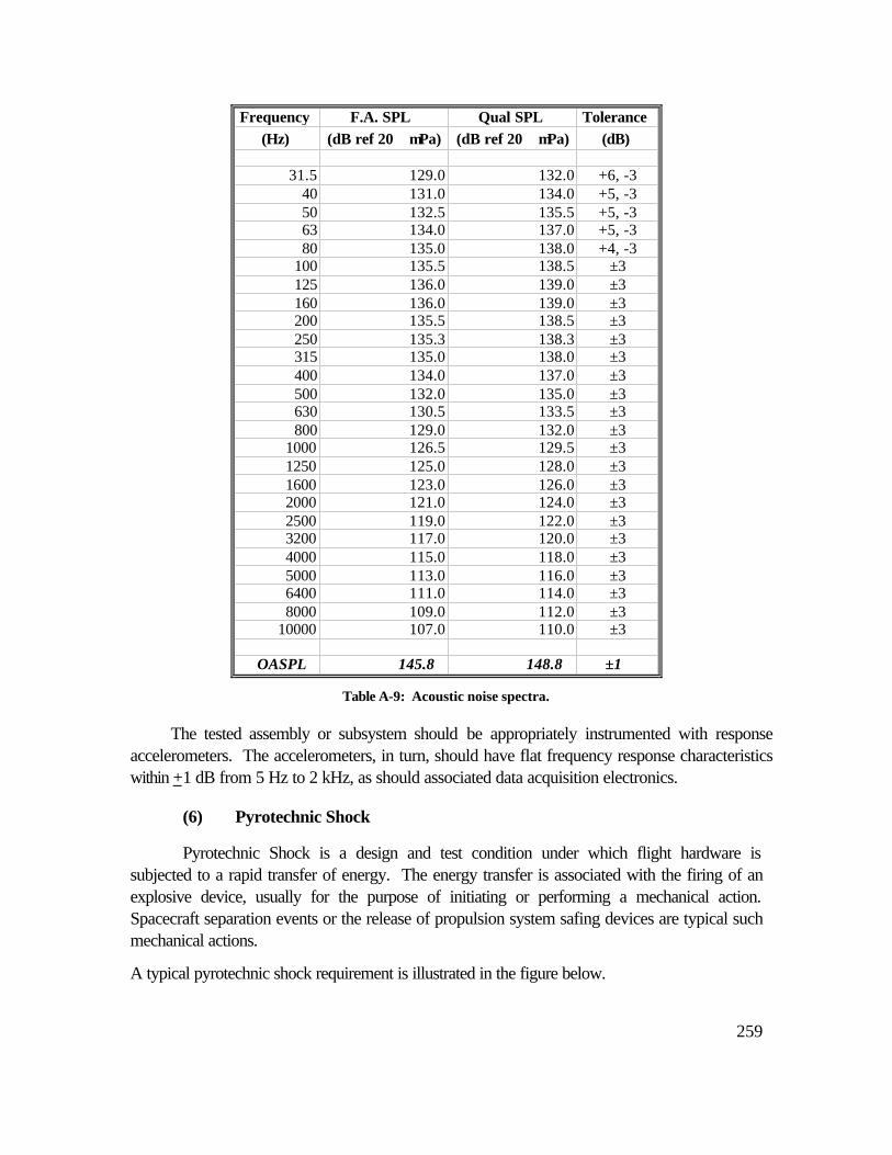
259
Frequency F.A. SPL Qual SPL Tolerance(Hz) (dB ref 20 µPa) (dB ref 20 µPa) (dB)
31.5 129.0 132.0 +6, -340 131.0 134.0 +5, -350 132.5 135.5 +5, -363 134.0 137.0 +5, -380 135.0 138.0 +4, -3
100 135.5 138.5 ±3125 136.0 139.0 ±3160 136.0 139.0 ±3200 135.5 138.5 ±3250 135.3 138.3 ±3315 135.0 138.0 ±3400 134.0 137.0 ±3500 132.0 135.0 ±3630 130.5 133.5 ±3800 129.0 132.0 ±3
1000 126.5 129.5 ±31250 125.0 128.0 ±31600 123.0 126.0 ±32000 121.0 124.0 ±32500 119.0 122.0 ±33200 117.0 120.0 ±34000 115.0 118.0 ±35000 113.0 116.0 ±36400 111.0 114.0 ±38000 109.0 112.0 ±3
10000 107.0 110.0 ±3
OASPL 145.8 148.8 ±1
Table A-9: Acoustic noise spectra.
The tested assembly or subsystem should be appropriately instrumented with responseaccelerometers. The accelerometers, in turn, should have flat frequency response characteristicswithin +1 dB from 5 Hz to 2 kHz, as should associated data acquisition electronics.
(6) Pyrotechnic Shock
Pyrotechnic Shock is a design and test condition under which flight hardware issubjected to a rapid transfer of energy. The energy transfer is associated with the firing of anexplosive device, usually for the purpose of initiating or performing a mechanical action.Spacecraft separation events or the release of propulsion system safing devices are typical suchmechanical actions.
A typical pyrotechnic shock requirement is illustrated in the figure below.
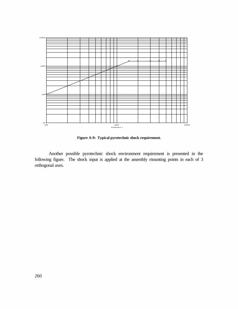
260
10
100
1000
10000
100 1000 10000
F r e q u e n c y H z
Figure A-9: Typical pyrotechnic shock requirement.
Another possible pyrotechnic shock environment requirement is presented in thefollowing figure. The shock input is applied at the assembly mounting points in each of 3orthogonal axes.
261
4 0 0 0 G ' s
6 5 G ' s
1 5 0 0 H z
Q = 10
9 d B / O c t a v e
10
100
1000
10000
100 1000 10000
F r e q u e n c y H z
CassiniGalilioMagellian TopTopexSeaWindsMars OMars GSMagellian BotMars PathRequirment+6 dB Tol-6 dB Tol
Figure A-10: Subassembly pyrotechnic shock design requirement.
This spectrum represents a 2σ environmental level. It is intended to encompass 95% ofall expected shock environments for all available launch vehicles. For reference, shock levelsfrom a number of previous programs are also indicated in the figure.
For test purposes, this environment should be considered a qualification level.Equipment should be exposed to the shock spectrum 3 times in each axis. For devices withself-contained ordinance, 3 self-induced shocks should also be applied.
The release of energy from an ordnance-containing device and the subsequent transferto the surrounding structure represents a very complex event. As a result, it is difficult todescribe the actual shape of the applied shock wave; it is generally not a simple time-basedpulse such as a square or triangular wave. The figure below illustrates a typical accelerationversus time trace from an actual pyrotechnic shock event.
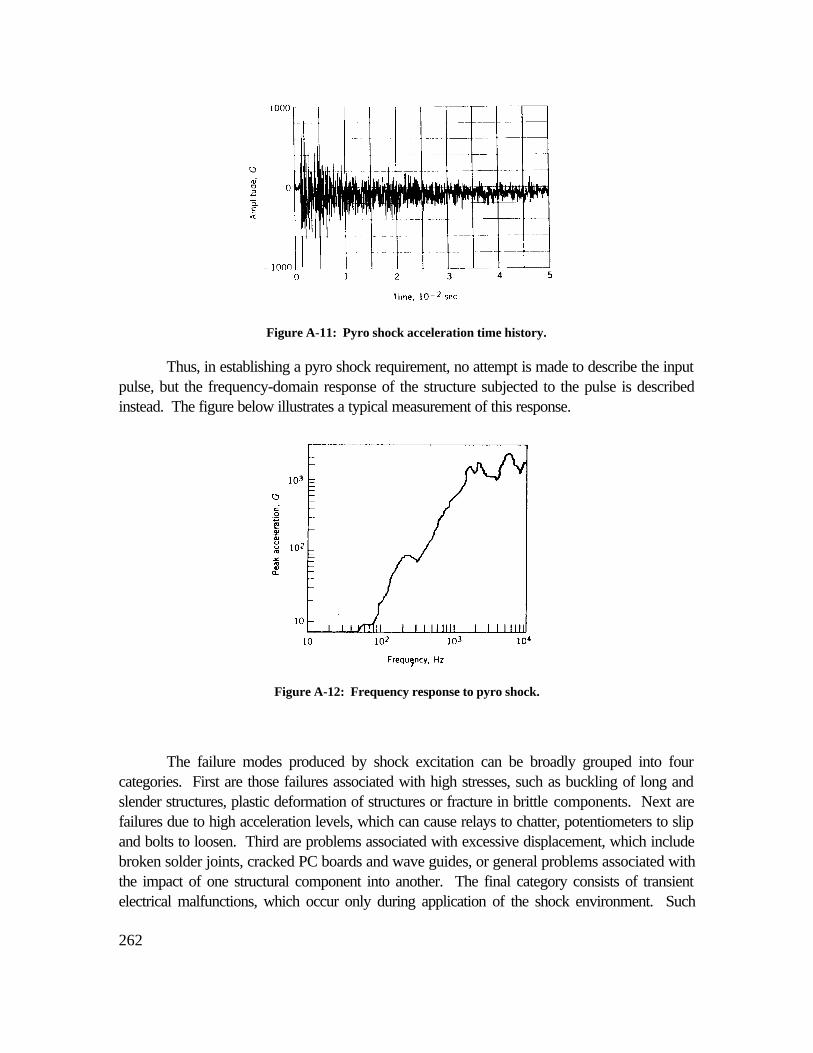
262
Figure A-11: Pyro shock acceleration time history.
Thus, in establishing a pyro shock requirement, no attempt is made to describe the inputpulse, but the frequency-domain response of the structure subjected to the pulse is describedinstead. The figure below illustrates a typical measurement of this response.
Figure A-12: Frequency response to pyro shock.
The failure modes produced by shock excitation can be broadly grouped into fourcategories. First are those failures associated with high stresses, such as buckling of long andslender structures, plastic deformation of structures or fracture in brittle components. Next arefailures due to high acceleration levels, which can cause relays to chatter, potentiometers to slipand bolts to loosen. Third are problems associated with excessive displacement, which includebroken solder joints, cracked PC boards and wave guides, or general problems associated withthe impact of one structural component into another. The final category consists of transientelectrical malfunctions, which occur only during application of the shock environment. Such
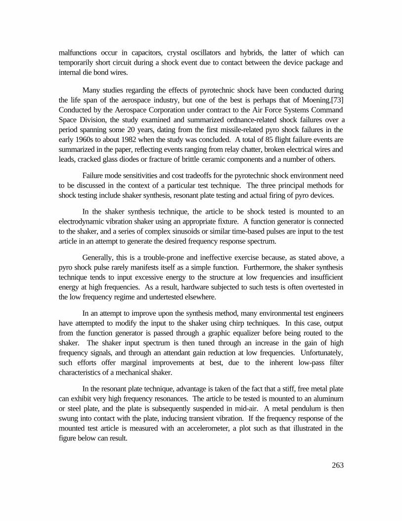
263
malfunctions occur in capacitors, crystal oscillators and hybrids, the latter of which cantemporarily short circuit during a shock event due to contact between the device package andinternal die bond wires.
Many studies regarding the effects of pyrotechnic shock have been conducted duringthe life span of the aerospace industry, but one of the best is perhaps that of Moening.[73]Conducted by the Aerospace Corporation under contract to the Air Force Systems CommandSpace Division, the study examined and summarized ordnance-related shock failures over aperiod spanning some 20 years, dating from the first missile-related pyro shock failures in theearly 1960s to about 1982 when the study was concluded. A total of 85 flight failure events aresummarized in the paper, reflecting events ranging from relay chatter, broken electrical wires andleads, cracked glass diodes or fracture of brittle ceramic components and a number of others.
Failure mode sensitivities and cost tradeoffs for the pyrotechnic shock environment needto be discussed in the context of a particular test technique. The three principal methods forshock testing include shaker synthesis, resonant plate testing and actual firing of pyro devices.
In the shaker synthesis technique, the article to be shock tested is mounted to anelectrodynamic vibration shaker using an appropriate fixture. A function generator is connectedto the shaker, and a series of complex sinusoids or similar time-based pulses are input to the testarticle in an attempt to generate the desired frequency response spectrum.
Generally, this is a trouble-prone and ineffective exercise because, as stated above, apyro shock pulse rarely manifests itself as a simple function. Furthermore, the shaker synthesistechnique tends to input excessive energy to the structure at low frequencies and insufficientenergy at high frequencies. As a result, hardware subjected to such tests is often overtested inthe low frequency regime and undertested elsewhere.
In an attempt to improve upon the synthesis method, many environmental test engineershave attempted to modify the input to the shaker using chirp techniques. In this case, outputfrom the function generator is passed through a graphic equalizer before being routed to theshaker. The shaker input spectrum is then tuned through an increase in the gain of highfrequency signals, and through an attendant gain reduction at low frequencies. Unfortunately,such efforts offer marginal improvements at best, due to the inherent low-pass filtercharacteristics of a mechanical shaker.
In the resonant plate technique, advantage is taken of the fact that a stiff, free metal platecan exhibit very high frequency resonances. The article to be tested is mounted to an aluminumor steel plate, and the plate is subsequently suspended in mid-air. A metal pendulum is thenswung into contact with the plate, inducing transient vibration. If the frequency response of themounted test article is measured with an accelerometer, a plot such as that illustrated in thefigure below can result.
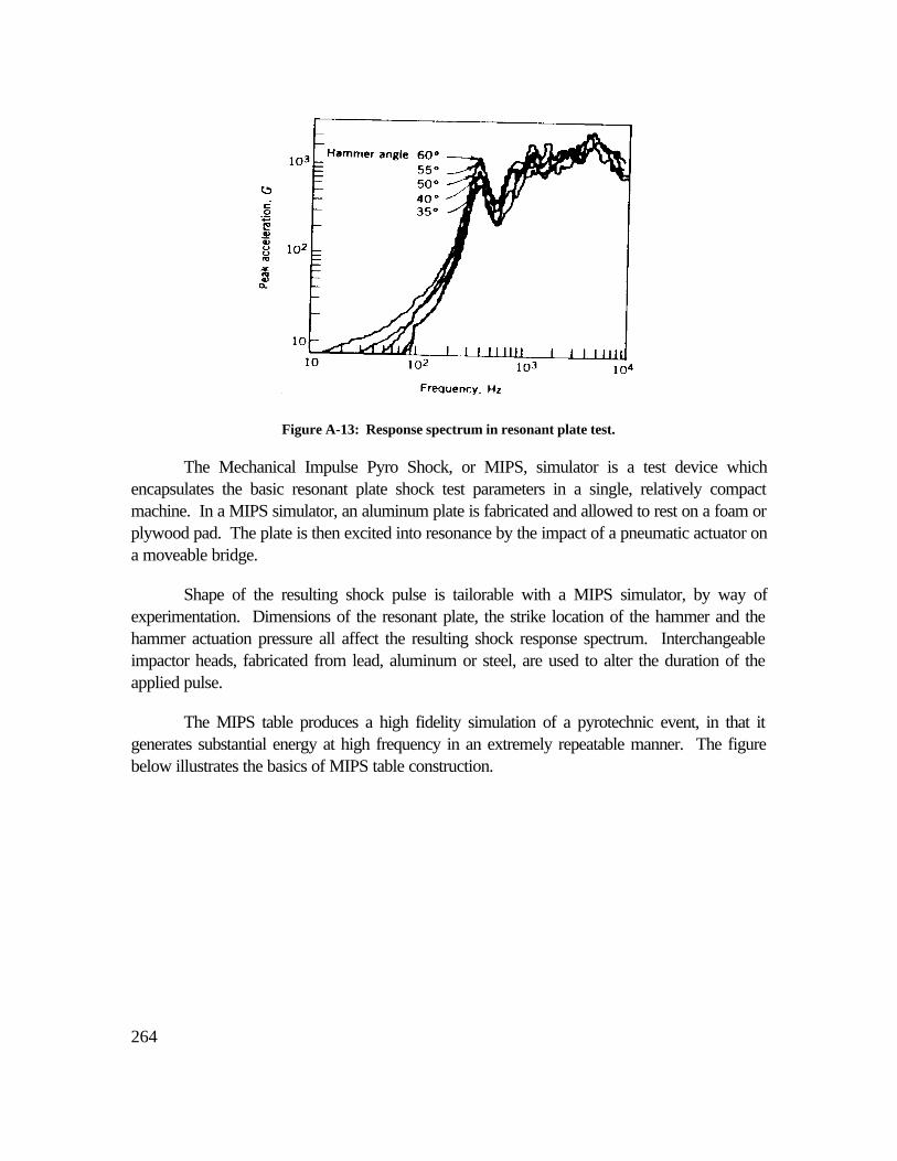
264
Figure A-13: Response spectrum in resonant plate test.
The Mechanical Impulse Pyro Shock, or MIPS, simulator is a test device whichencapsulates the basic resonant plate shock test parameters in a single, relatively compactmachine. In a MIPS simulator, an aluminum plate is fabricated and allowed to rest on a foam orplywood pad. The plate is then excited into resonance by the impact of a pneumatic actuator ona moveable bridge.
Shape of the resulting shock pulse is tailorable with a MIPS simulator, by way ofexperimentation. Dimensions of the resonant plate, the strike location of the hammer and thehammer actuation pressure all affect the resulting shock response spectrum. Interchangeableimpactor heads, fabricated from lead, aluminum or steel, are used to alter the duration of theapplied pulse.
The MIPS table produces a high fidelity simulation of a pyrotechnic event, in that itgenerates substantial energy at high frequency in an extremely repeatable manner. The figurebelow illustrates the basics of MIPS table construction.
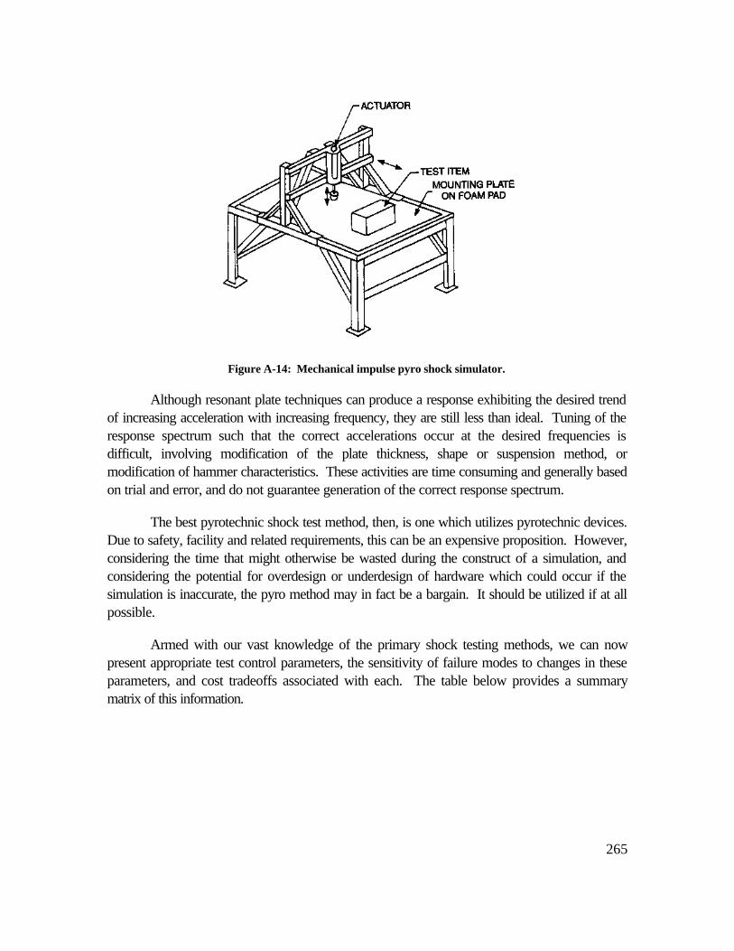
265
Figure A-14: Mechanical impulse pyro shock simulator.
Although resonant plate techniques can produce a response exhibiting the desired trendof increasing acceleration with increasing frequency, they are still less than ideal. Tuning of theresponse spectrum such that the correct accelerations occur at the desired frequencies isdifficult, involving modification of the plate thickness, shape or suspension method, ormodification of hammer characteristics. These activities are time consuming and generally basedon trial and error, and do not guarantee generation of the correct response spectrum.
The best pyrotechnic shock test method, then, is one which utilizes pyrotechnic devices.Due to safety, facility and related requirements, this can be an expensive proposition. However,considering the time that might otherwise be wasted during the construct of a simulation, andconsidering the potential for overdesign or underdesign of hardware which could occur if thesimulation is inaccurate, the pyro method may in fact be a bargain. It should be utilized if at allpossible.
Armed with our vast knowledge of the primary shock testing methods, we can nowpresent appropriate test control parameters, the sensitivity of failure modes to changes in theseparameters, and cost tradeoffs associated with each. The table below provides a summarymatrix of this information.
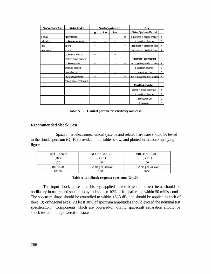
266
Control Parameters Failure Modes Sensitivity to Increase Cost
g tdur trise f Shaker Synthesis Method
g peak intermittents + - - 0 g increase = bigger shaker +
t duration broken solder joints + + + - t duration change 0
t rise opens + - - + t rise redct = better fct gen +
frequency shorts + - - + f increase = chirp test eqpt +
broken connectors + - + -
broken wave guides + - + - Resonant Plate Method
broken crystals + - - + g incr = plate/pendlm change +
cracked diodes + - - + t duration change 0
relay chatter + - - + t rise reduction 0
fastener loosening + - - + f incr = plate/pendlm change +
potentiometer slippage + - - +
Pyro Device Method
g incr = charge change +
t duration change 0
t rise reduction 0
f increase 0
Table A-10: Control parameter sensitivity and cost.
Recommended Shock Test
Space microelectromechanical systems and related hardware should be testedto the shock spectrum (Q=10) provided in the table below, and plotted in the accompanyingfigure.
FREQUENCY(Hz)
ACCEPTANCE(G PK)
PROTOFLIGHT(G PK)
100 40 60100-1500 9.2 dB per Octave 9.2 dB per Octave
10000 2500 3750
Table A-11: Shock response spectrum (Q=10).
The input shock pulse time history, applied to the base of the test item, should beoscillatory in nature and should decay to less than 10% of its peak value within 50 milliseconds.The spectrum shape should be controlled to within +6/-3 dB, and should be applied in each ofthree (3) orthogonal axes. At least 30% of spectrum amplitudes should exceed the nominal testspecification. Components which are powered-on during spacecraft separation should beshock tested in the powered-on state.
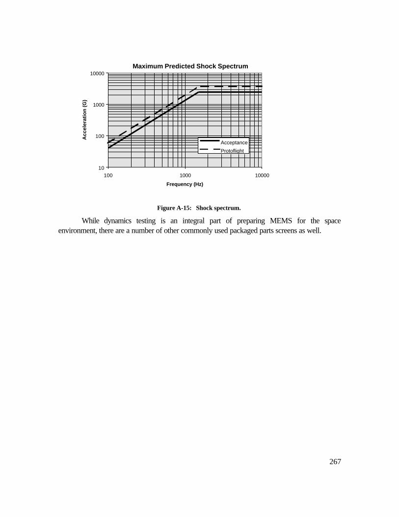
267
Maximum Predicted Shock Spectrum
10
100
1000
10000
100 1000 10000
Frequency (Hz)
Acc
eler
atio
n (
G)
Acceptance
Protoflight
Figure A-15: Shock spectrum.
While dynamics testing is an integral part of preparing MEMS for the spaceenvironment, there are a number of other commonly used packaged parts screens as well.

268

269
Index
A
Aluminum, 60, 61, 75
B
bandgap, 49, 50, 52, 54, 55brittle, 19, 24, 30, 31, 32, 48, 52, 58, 151, 238, 239Bulk Micromachining, 78
C
cantilever, 34, 39, 85, 97, 100, 101, 105, 119, 134, 148, 149, 171, 172, 174, 176, 178, 208,8
capacitors, 93, 129, 130, 131, 132, 238Chemical Vapor Deposition, 70CMOS, 84, 85, 86, 87, 95, 147, 1, 7Comb Drives, 133Copper, 62, 63crystal, 19, 21, 22, 23, 24, 25, 26, 28, 29, 30, 33, 39, 46, 48, 50, 51, 58, 71, 75, 76, 78,
118, 120, 141, 238crystals, 20, 25, 26, 27, 71
D
device structures, ivDislocation
Edge, 28Screw, 28
Dislocations, 28dynamics, 168, 214, 215, 216, 220, 243
E
ESD, 194, 196, 209, 211Etching, 73, 75
Dry, 75Wet, 73
Euler-Bernoulli equation, 95Evaporation. See Thin Film: Evaporation
270
F
Failure, 17, 18, 19, 37, 101, 112, 196, 203, 204, 211, 212, 213, 233, 239, 9failure mechanisms, ii, iv, 15, 17, 19, 37, 46, 157, 171, 204Finite Element Analysis, 157, 164Fracture, 19, 30, 47, 54, 57, 4
G
gallium arsenide, 56, 59, 89Gold, 61, 62, 127
H
Harmonic Motors, 139Heat Transfer Analysis, 158Hinges, 115, 117, 7Hooke’s law, 98
I
Interstitial, 27
L
lamb waves, 109Lift-off, 73LIGA, 87, 88, 89, 177linear, 24, 31, 40, 44, 97, 98, 102, 121, 132, 141, 148, 164, 167, 168, 181
M
Magnetic Actuators, 142Mask Fabrication, 72Material properties, ivmembrane, 90, 105, 106, 109, 112, 116, 120, 121MEMS. See microelectromechanical systemsmicroelectromechanical systems, ivMicromotors, 138Modal Analysis, 166
N
natural frequency, 42, 100

271
P
Parallel Plate Capacitors, 129, 132photolithography, 72, 73Piezoresistivity, 118piezoresistors, 120, 121PMMA, 88Point Defects, 26Point Replacement, 27Poisson’s ratio, 22, 23, 55, 57, 61, 62, 107, 157Polyimides, 63, 64processing techniques, ii, iv, 65, 78, 89
Q
qualification methodologies, iv
R
radiation, 3, 39, 49, 88, 126, 184, 205, 218Reactive Growth. See Thin Film: Reactive GrowthReliability, i, ii, 4, 6, 117, 121, 127, 140, 145, 150, 1, 3, 4, 6, 7resonant frequency, 32, 37, 42, 43, 44, 99, 100, 110, 174
S
Shape memory alloy, 149silicon, 22, 25, 31, 40, 41, 46, 48, 49, 50, 51, 52, 54, 55, 56, 58, 59, 63, 65, 68, 69, 70, 75,
76, 77, 78, 79, 80, 85, 89, 118, 119, 120, 122, 141, 160, 162, 163, 8silicon nitride, 33, 54, 55, 70, 78, 79, 89Spin Casting, 65Sputtering. See Thin Film: SputteringStatic Analysis, 165strain, 19, 20, 24, 55, 60, 91, 119, 161, 162, 163, 164, 176, 228Stress, 19, 24, 60, 112, 160, 161, 164, 169, 175, 177, 4, 5
concentration factor, 24Structural Beams, 94, 101Surface Micromachining, 80
T
Test Structures, 171Thermal Actuators, 147Thermal Fatigue Stress Analysis, 161Thin Film, 65
272
Chemical Vapor Deposition, 70Evaporation, 66Growth and Deposition, 65Reactive Growth, 68Spin Casting, 65Sputtering, 66
thin films, 41, 46, 50, 65, 68, 113, 178, 179Tunneling Tips, 124
V
Vacancies, 26
W
Wafer Bonding, 76Anodic Bonding, 76Fusion Bonding, 77Low-Temperature Glass Bonding, 77
Y
yield strength, 26, 35, 60Young’s modulus, 20, 33, 40, 54, 55, 86, 95, 149, 174, 3, 4
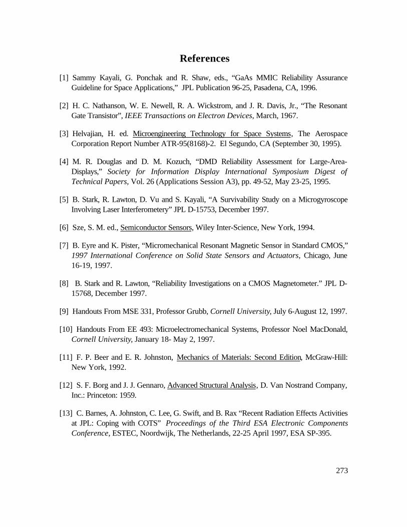
273
References
[1] Sammy Kayali, G. Ponchak and R. Shaw, eds., “GaAs MMIC Reliability AssuranceGuideline for Space Applications,” JPL Publication 96-25, Pasadena, CA, 1996.
[2] H. C. Nathanson, W. E. Newell, R. A. Wickstrom, and J. R. Davis, Jr., “The ResonantGate Transistor”, IEEE Transactions on Electron Devices, March, 1967.
[3] Helvajian, H. ed. Microengineering Technology for Space Systems, The AerospaceCorporation Report Number ATR-95(8168)-2. El Segundo, CA (September 30, 1995).
[4] M. R. Douglas and D. M. Kozuch, “DMD Reliability Assessment for Large-Area-Displays,” Society for Information Display International Symposium Digest ofTechnical Papers, Vol. 26 (Applications Session A3), pp. 49-52, May 23-25, 1995.
[5] B. Stark, R. Lawton, D. Vu and S. Kayali, “A Survivability Study on a MicrogyroscopeInvolving Laser Interferometery” JPL D-15753, December 1997.
[6] Sze, S. M. ed., Semiconductor Sensors, Wiley Inter-Science, New York, 1994.
[7] B. Eyre and K. Pister, “Micromechanical Resonant Magnetic Sensor in Standard CMOS,”1997 International Conference on Solid State Sensors and Actuators, Chicago, June16-19, 1997.
[8] B. Stark and R. Lawton, “Reliability Investigations on a CMOS Magnetometer.” JPL D-15768, December 1997.
[9] Handouts From MSE 331, Professor Grubb, Cornell University, July 6-August 12, 1997.
[10] Handouts From EE 493: Microelectromechanical Systems, Professor Noel MacDonald,Cornell University, January 18- May 2, 1997.
[11] F. P. Beer and E. R. Johnston, Mechanics of Materials: Second Edition, McGraw-Hill:New York, 1992.
[12] S. F. Borg and J. J. Gennaro, Advanced Structural Analysis, D. Van Nostrand Company,Inc.: Princeton: 1959.
[13] C. Barnes, A. Johnston, C. Lee, G. Swift, and B. Rax “Recent Radiation Effects Activitiesat JPL: Coping with COTS” Proceedings of the Third ESA Electronic ComponentsConference, ESTEC, Noordwijk, The Netherlands, 22-25 April 1997, ESA SP-395.
274
[14] D. Maier-Scheider, J. Maibach, and E. Obermeier, “A New Analytical Solution for theLoad-Deflection of Square Membranes” Journal of Microelectromechanical Systems,Vol. 4, No. 4, December 1995.
[15] J. W. Judy and R. S. Muller, “Magnetically Actuated Addressable Microstructures”,Journal of Microelectromechanical Systems, Vol. 6, No. 3, September 1997.
[16] K. E. Peterson, “Silicon as a Mechanical Material” Proceedings of the IEEE, May1982.
[17] K. Hjort, J. Söderkvist and J. Schweitz, “Gallium Arsenide as a Mechanical Material”Journal of Micromechanics and Microengineering Vol. 4, No. 1, January 1994.
[18] John T. Milek, Silicon Nitride for Microelectronics Applications, IFI/Plenum, New York,1971.
[19] U. Beerschwinger, D. Mathieson, R. L. Reuben, and S. J. Yang, “A study of Wear onMEMS Contact Morphologies” Journal of Micromechanics and Microengineering Vol.7, September 1994.
[20] W. H. Ko, J. T. Suminto and G. J. Yeh, “Bonding Techniques for Microsensors,”Micromachining and Micropackaging of Transducers, C. D. Fung, P. W. Cheung, W.H. Ko, and D. G. Fleming, Eds. p. 41.
[21] K. Fricke, J. Würfl, J. Miao, A. Dehé, D. Rück, and H. L. Hartnagel, “Fabrication ofMicrostructures for Integrated Sensors on GaAs,” Journal of Micromechanics andMicroengineering Vol. 3, pp. 131-134, 1993.
[22] L. S. Fan, Y. C. Tai, and R. S. Muller, “IC-Processed Electrostatic Micro-motors.”IEEE International Electronic Devices Meeting, December 1988.
[23] Y. C. Tai, L. S. Fan, and R. S. Muller, “IC-Processed Micro-motors: Design,Technology, and Testing” Proceedings of IEEE Microelectromechanical Systems,February 1989.
[24] W. C. Tang, T-C. H. Nguyen, and R. T. Howe. “Laterally Driven Polysilicon ResonantMicrostructures.” Proceedings of IEEE Microelectromechanical Systems, February1989.
[25] C. J. Kim, A. P. Pisano, R. S. Muller, and M. G. Lim, “Polysilicon Microgripper”.Technical Digest IEEE Solid-State Sensor and Actuator Workshop, June 1990.
275
[26] F. Ericson, S. Greek, J. Söderkvist and J. Schweitz, “High-sensitivity surfacemicromachined structures for internal stress and stress gradient evaluation”. Journal ofMicromechanics and Microengineering, Vol. 7, 1997.
[27] A. T. DiBenedetto, The Structure and Properties of Materials, McGraw-Hill, UnitedStates of America, 1967.
[28] Interview with Jim Okuno on 11-19-97
[29] C. Barnes, C. Lee, A. Johnston, and R. Lawton, “Radiation Issues for MEMS” MEMSReliability and Qualification Workshop, Pasadena, CA 1997.
[30] Y. Gianchandani and K. Najafi, “Bent-Beam Strain Sensors” Journal ofMicroelectromechanical Systems, Vol. 5, No. 1, March 1996.
[31] MIL-STD-45662, Calibration System Requirements, Department of Defense,Washington, DC 1988.
[32] J. G. Collins, W. J. Giardini, A. J. Leistner, and M. J. Kenny “The Influence of Young’sModulus on the Roundness in Silicon Sphere Fabrication” IEEE Transactions onInstrumentation and Measurement, Vol. 46, No.2 April 1997.
[33] Distributor Requirements for Handling Electrostatic Discharge Sensitive (ESDS)Devices, JEDEC Publication EIA 625, EIA & JEDEC Standards & EngineeringPublications, 1994.
[34] MIL-STD-1686, Electrostatic Discharge Control Program for Protection ofElectrical and Electronic Parts, Assemblies and Equipment (Excluding ElectricallyInitiated Explosive Devices), Department of Defense, Washington, DC, 1992.
[35] General Standards For Statistical Process Control, JEDEC Publication EIA 557A,EIA & JEDEC Standards & Engineering Publications, 1995.
[36] MIL-I-38535B, Integrated Circuits (Microcircuits) Manufacturing, Department ofDefense, Washington, DC, June 1, 1993.
[37] J. Weertman and J. R. Weertman, Elementary Dislocation Theory. Oxford UniversityPress, New York, 1992.
[38] MIL-STD-8883, Test Methods and Procedures for Microelectronics, Department ofDefense, Washington, DC, November 15, 1991.
276
[39] Transistor, Gallium Arsenide Power FET, Generic Specification, JEDEC Publication,JES2, July 1992, EIA & JEDEC Standards & Engineering Publications.
[40] F. Ericson and J. Å. Schweitz, “Micromechanical Fracture Strength of Silicon” Journalof Applied Physics. Vol. 68 pp. 5840-4, 1990.
[41] T. W. Kenny, W. J. Kaiser, H.K. Rockstad, J. K. Reynolds, J. A. Podosek, and E. C.Vote, “Wide-Bandwidth Electromechanical Actuators for Tunneling DisplacementTransducers” Journal of Microelectromechanical Systems, Vol. 3, No. 3, September1994.
[42] B. Stark, R. Lawton, J. Schiff, T. George, L. Miller, and L. Muller, “Reliability Evaluationof Tunneling Technology for MEMS Devices” JPL D-14729, December 1997.
[43] P. G. Hartwell, F. M. Bertsch, S. A. Miller, K. L. Turner, and N. C. MacDonald, “SingleMask Lateral Tunneling Accelerometer”, Proceedings of 11th Intl. Workshop on MEMS,Heidelberg, Germany, January 25-29, 1998.
[44] J. Koskinun, J. E. Steinwall, R. Soave and H. H. Johnson, “Microtensile Testing of Free-standing Polysilicon Fibers of Various Grain Sizes”, Journal of Micromechanics andMicroengineering, Vol. 3 March 1993.
[45] W. C. Tang, “Micromechanical Devices: Technology and Reliability Implications”Microelectronics Reliability and Qualification Workshop, June 16-17, 1998.
[46] S. A. Campbell The Science and Engineering of Microelectronic Fabrication OxfordUniversity Press, Oxford, 1996.
[47] C. J. Wilson and P. A. Beck, “Fracture Testing of Bulk Silicon Microcantilever BeamsSubjected to a Side Load” Journal of Microelectromechanical Systems, Vol. 5, No. 3,September 1996.
[48] W. A. Brantley, “Calculated Elastic Constants for Stress Problems Associated withSemiconductor Devices”, Journal of Applied Physics, Vol. 44, No. 1 January 1973.
[49] J. J. Wortman and R. A. Evans “Young’s Modulus, Shear Modulus, and Poisson’s Ratioin Silicon and Germanium”, Journal of Applied Physics, Vol. 36, No. 1 January 1965.
[50] D. M. Tanner, N. F. Smith, D. J. Bowman, W. P. Eaton, and K. A Peterson, “FirstReliability Test of a Surface Micromachined Microengine Using SHiMMeR” Proceedingsof SPIE, Vol. 3224, PP 14-23, 1997.
277
[51] S. W. Wenzel and R. M. White, “A Multisensor Employing an Ultrasonic Lamb-WaveOscillator”, IEEE Transactions on Electron Devices, vol. 35, No.6, June 1988.
[52] W. Riethmüller and W Benecke, “Thermally Excited Silicon Microactuators” IEEETransactions on Electron Devices, Vol. 35, No. 6, June 1988.
[53] H. G. Van Bueren, Imperfections In Crystals, North-Holland Publishing Company,Amsterdam, 1960.
[54] C. M. Harris and C. E. Crede, Shock and Vibration Handbook Volume 1: Basic Theoryand Measurements, McGraw-Hill Book Company, Inc., New York, 1961.
[55] W. Trimmer “Microrobots and Micromechanical systems” Sensors and Actuators,Vol.19, No. 3, pp. 267-287, September 1987.
[56] W. Trimmer Micromechanics and MEMS: Classical and Seminal Papers to 1990, IEEEPress, New York, 1997.
[57] P. A. Neukomm, H. P. Bornhauser, T. Hochuli, R. Paravicini, and G. Schwarz,“Characteristics of Thin-wire Shape Memory Actuators” Transducers ’89, Proceedings ofthe 5th International Conference on Solid-State Sensors and Actuators, Vol. 2, pp.247-252, June 1990.
[58] S. Timoshenko and Woinowsky-Krieger, Theory of Plates and Shells, 2nd. edition, NewYork: McGraw-Hill, 1959
[59] R. Roark, R. and W. Young, Roark’s Formulas for Stress and Strain, 6th edition, NewYork: McGraw-Hill, 1989
[60] J. Sigley and C. Mischke, Mechanical Engineering Design, 5th edition, New York:McGraw-Hill, 1989.
[61] R. Blevins, Formulas for Natural Frequency and Mode Shape, New York: Van NostrandReinhold, 1979.
[62] Newell, J., Larson, T. and Cornford S., “A Thermo-mechanical Stress Analysis of anMCM-D Interconnect,” Proceedings of the Pan Pacific Microelectronics Symposium,Honolulu, HI, February 1996.
[63] MIL-STD-1540C, Test Requirements for Launch, Upper-Stage and Space Vehicles,United States Air Force Military Standard, 1994.
278
[64] Thomson, W. T., “Theory of Vibration with Applications,” 2nd ed., Prentice-Hall, Inc.,Engelwood Cliffs, N.J., 1981.
[65] Meirovitch, L., “Elements of Vibration Analysis,” 2nd ed., McGraw-Hill Book Company,New York, 1986.
[66] Steinberg, D. S., “Vibration Analysis for Electronic Equipment,” John Wiley & Sons, Inc.,New York, 1986.
[67] Harris, C. M. (ed.), “Shock and Vibration Handbook,” 4th ed., McGraw-Hill BookCompany, New York, 1996.
[68] Marks, L. S. and T. Baumeister, “Mechanical Engineer’s Handbook,” 6th ed., McGraw-Hill Book Company, New York, 1958.
[69] Kreith, F. and W. Black, “Basic Heat Transfer,” Harper & Row, New York, 1980.
[70] Kinsler, L. E. and A. R. Frey, “Fundamentals of Acoustics,” 2nd ed., John Wiley & Sons,Inc., New York, 1962.
[71] Himelblau, H., C. Fuller and T. Scharton, “Assessment of Space Vehicle AeroacousticVibration Prediction, Design and Testing,” NASA CR-1596, July, 1970.
[72] NASA-STD-7001, Payload Vibroacoustic Test Criteria, National Aeronautics andSpace Administration Technical Standard, June 21, 1996.
[73] Moening, C. J., “Pyrotechnic Shock Flight Failures”, IES Pyrotechnic Shock TutorialProgram, 31st ATM, Institute of Environmental Sciences, April-May 1985.
[74] Markstein, H. W., “Designing Electronics for High Vibration and Shock,” ElectronicPackaging & Production, April 1987, pp. 40-43.
[75] White, D. and M. Mardiguian, “EMI Control Methodology and Procedures,” 4th ed.,Interference Control Technologies, Gainesville, Virginia, 1986.
[76] MIL-STD-461, Electromagnetic Emission and Susceptibility Requirements for theControl of Electromagnetic Interference, United States Department of Defense MilitaryStandard, 1986.
[77] MIL-STD-462, Electromagnetic Emission and Susceptibility, Test Methods for,United States Department of Defense Military Standard.
[78] NASA Preferred Reliability Practice No. PT-TE-1406, “Sinusoidal Vibration.”
279
[79] NASA Preferred Reliability Practice No. PT-TE-1408A, “Pyrotechnic Shock Testing,”May 1996.
[80] NASA Preferred Reliability Practice No. PT-TE-1412, “Environmental Test Sequencing.”
[81] NASA Preferred Reliability Practice No. PT-TE-1413, “Random Vibration Testing.”
[82] NASA Preferred Reliability Practice No. PT-TE-1431, “Voltage & Temperature MarginTesting,” September 1995.
[83] Wilkerson, T. D., M. Lauriente and G. Sharp, “Space Shuttle Environment,” EngineeringFoundation, New York, 1985.
[84] S. L. Miller, G. LaVigne, M. S. Rodgers, J. J. Sniegowski, J. P. Waters, and P. J.McWhorter, “Routes to failure in rotating MEMS devices experiencing sliding friction”,Proceeding of SPIE Micromachined Devices and Components III, Vol. III, Austin,Sept. 29-30, pp. 24-30.
[85] Michelle M. Gauthier, Engineering Materials Handbook, ASM desk edition. MaterialsPark, OH, Nov 1995.
[86] Handouts provided by G. Fedder, Carnegie-Mellon University.
[87] S. C. Jacobsen, R. H. Price, J. E. Wood, T. H. Rytting, and M. Rafaelof, “The WobbleMotor: An Electrostatic, Planetary Armature, Microactuator” Proceedings of IEEEMicroelectromechanical Systems, pp. 17-24, February 1989.
[88] M. Mehregany, P. Nagarhar, S. Senturia, and J. Lang, “Operation of MicrofabricatedHarmonic and Ordinary Side-Drive Motors” Proceedings of IEEEMicroelectromechanical Systems, pp. 1-8, February 1990.
[89] W. S. Trimmer, K. J. Gabriel, and R. Mahadevan, “Silicon Electrostatic Motors”,Transducers ’87, The 4th International Conference of Solid-State Sensors andActuators, pp. 857-860, June 1987.
[90] W. S. Trimmer and K. J. Gabriel, “Design Considerations for a Practical ElectrostaticMicro-Motor”, Sensors and Actuators, Vol. 11, pp. 189-206, 1987.
[91] Y. Kanda, “A Graphical Representation of the Piezoresistive Coefficients in Silicon”,IEEE Transactions on Electron Devices, Vol. ED-29, No. 1, January 1982.
[92] J. Schiff, B. Eyre, and R. Lawton, “Delamination Effects on Resonant Frequency in aCMOS Magnetometer”, JPL Internal Document, August 1997.
280
[93] K. S. Pister, M. W. Judy, S. R. Burgett, and R. S. Fearing, “Microfabricated Hinges”Sensors and Actuators A, Vol. 33, pp. 249-256, 1992.
[94] L. Y. Lin, S. S. Lee, K. S. Pister, and M. C. Wu, “Micro-Machined Three-DimensionalMicro-Optics for Integrated Free-Space Optical System”, IEEE Photonics Letters, Vol.6, No. 12, December 1994.
[95] M. Tabib-Azar, K. Wong, and W. Ko, “Aging Phenomena in heavily doped (p+)micromachined silicon cantilever beams”, Sensors and Actuators A, Vol. 33, pp. 199-206,1992.
[96] J. B. Angell, S. C. Terry, and P. W. Barth, “Silicon Micromechanical Devices”, ScientificAmerican Journal, April 1983.
[97] R. E. Pelrine, “Room Temperature, Open-Loop Levitation of Microdevices UsingDiamagnetic Materials”, Proceedings of IEEE Microelectromechanical Systems, pp. 34-37, February 1990.
[98] R. E. Pelrine and I. Busch-Vishniac “Magnetically Levitated Micro-Machines”, IEEEMicro Robots and Teleoperators, November 1987.
[99] J. W. Judy and R. S. Muller, “Magnetic Microactuation of torsional polysiliconstructures,” Sensors and Actuators A, Physical, vol. A53, nos. 1-3, pp. 392-397, 1996.
[100] Krane, K, Modern Physics, John Wiley & Sons, New York, 1996.
[101] Mechanics of Materials 23 1996.
[102] IEEE Microelectromechanical Systems Workshop, Feb 1993, Florida.
[103] T. Tsuchiya, O. Tabata, J. Sakata, and Y. Taga, “Specimen Size Effect on TensileStrength of Surface-Micromachined Polycrystalline Silicon Thin Films” Journal ofMicroelectromechanical Systems, Vol. 7, No.1, March 1998.
[104] D. G. Oei and S. McCarthy, “The effect of Temperature and Pressure on residual stressin LPCVD polysilicon films,” 1992 Materials Research Society Conference, p. 397.
[105] M. Sekimoto, H. Yoshihara, and T. Ohkubo, “Silicon Nitride Single-Layer X-RayMask.” Journal of Vacuum Science and Technology, Vol. 21, p 1017, 1982.
[106] J. W. Judy, D. L. Polla, and W. P. Robbins, “Experimental Model and IC-ProcessDesign of a Nanometer Linear Piezoelectric Stepper Motor” Microstructures, Sensorsand Actuators, DSC-Vol. 19, pp. 11-17, November 1990.
[107] K. Ikuta, S. Aritomi, and T. Kabashima, “Tiny Silent Linear Cybernetic Actuator Drivenby Piezoelectric Device with Electromagnetic Clamp”, Proceedings IEEEMicroelectromechanical Systems, pp. 232-237, February 1992.
281
[108] E. A. Amerasekera and F. N. Najm, Failure Mechanisms in Semiconductor Devices:Second Edition, John Wiley & Sons, New York, 1997.
[109] S. Kayali “Methodology for MEMS Reliability Evaluation and Qualification” MEMSReliability and Qualification Workshop, Pasadena, CA, August 5, 1997.
[110] R. Maboudian and R. T. Howe, “Critical Review: Adhesion in Surface MicromechanicalStructures” Journal of Vacuum Science and Technology B, Vol. 15, January 1997.
[111] Metals Handbook: 9th Ed. Vol. 2: Properties and Selection of Nonferrous Alloys andPure Metals, American Society for Metals, 1979.
[112] D. Bloor, R. J. Brook, M. C. Flemings and S. Mahajan, eds. The Encyclopedia ofAdvanced Materials, Elsevier Science, Ltd., New York: 1994.
[113] Presentation by Dr. Virgil Shields, “Silicon Carbide Gas Sensors for EnvironmentalContaminates.” Pasadena, July 9, 1998.
[114] C. Marxer, M.-A. Grétillat, N. F. de Rooij, R. Bättig, O. Anthamatten, B. Valk and P.Vogel, “Reliability considerations for electrostatic polysilicon actuators using as an examplethe REMO component” Sensors and Actuators A, Vol. 61, pp. 449-454, 1997.
[115] I. A. Viktorov, Rayleigh and Lamb Waves: Physical Theory and Applications, PlenumPress: New York, 1967.
[116] J. Zheng, S. Takahashi, S. Yoshikawa, and K. Uchino, “Heat Generation in MultilayerPiezoelectric Actuators” Journal of the American Ceramics Society, Vol. 79, No. 12,1996.
[117] B. W. Chui, T. D. Stowe, Y. S. Ju, K. E. Goodson, T. W. Kenny, H. J. Mamin, B. D.Terris, R. P. Ried, and D. Rugar, “Low-Stiffness Silicon Cantilevers with Integrated Heatersand Piezoresistive Sensors for High-Density AFM Thermomechanical Data Storage”Journal of Microelectromechanical Systems, Vol. 7 No. 1, March 1998.
[118] D. C. Montgomery and G. C. Runger, Applied Statistics and Probability for Engineers,John Wiley & Sons: New York, 1994.
[119] L. J. Broutman and R. H. Krock, Modern Composite Materials, Addison Wesley,Reading, Massachusetts: 1967.
[120] E. Rabinowicz, Friction and Wear of Materials: 2nd Edition, New York, John Wiley &Sons, 1995.
[121] D. M. Tanner, W. M. Miller, W. P. Eaton, L. W. Irwin, K. A. Peterson, M. T. Dugger,D. C. Senft, N. F. Smith, P. Tangyunyong, and S. L. Miller, “The Effect of Frequency on
282
the Lifetime of a Surface Micromachined Microengine Driving a Load” 1998 IEEEInternational Reliability Physics Symposium Proceedings, March 30-April 2, 1998, pp.26-35.
[122] L. D. Edmonds, C. I. Lee, and G. M. Swift, “Radiation Response of MEMSAccelerometer: An Electrostatic Force” 1998 National Space and Radiation EffectsConference, July 20-24, 1998.
[123] A. R. Knudson, S. Buchner, P. McDonald, W. J. Stapor, A. B. Campbell, K. S.Grabowski, D. L. Knies, S. Lewis, and Y. Zhao, “The Effects of Radiation on MEMSAccelerometers,” IEEE Transactions on Nuclear Science, vol. 43, pp. 3122-3125,December, 1996.
[124] J. S. Danel, F. Michel, and G. Delapierre, “Micromachining of Quartz and its applicationto an Acceleration Sensor” Sensors and Actuators A, Vol. A21-A23, pp. 971-977,1990.
[125] J. Söderkvist, “Micromachining of Quartz and its application to an Acceleration Sensor”Sensors and Actuators A, Vol. A21-A23, pp. 971-977, 1990.
[126] J.-A. Schweitz “Mechanical characterization of thin films by micromechanical techniques”MRS Bulletin, Vol.17, no.7, p. 34-45.
[127] T. Tsuchiya, O. Tabata, J. Sakata and Y. Taga, “Tensile Testing of PolycrystallineSilicon Thin Films Using Electrostatic Force Grip” Transactions of the Institute ofElectrical Engineers of Japan, Part E, Vol.116-E, no.10, p. 441-6.
[128] S. Greek, F. Ericson, S. Johansson and J.-A. Schweitz, “In situ tensile strengthmeasurement of thick-film and thin-film micromachined structures” 8th InternationalConference on Solid-State Sensors and Actuators and Eurosensors IX, Vol. 2, 1995.
[129] E. Obermeier, “Mechanical and Thermophysical Properties of Thin Film Materials forMEMS: Techniques and Devices” Materials Research Society Symposium Proceedings,Vol. 444.
[130] D. W. Burns, Micromechanics of Integrated Sensors and the Planar ProcessedPressure Transducer, Ph.D. Thesis, University of Wisconsin, Madison, 1988.
[131] E. D. Nicholson and J. E. Field, “The Mechanical and Thermal Properties of Thin Films”Journal of Hard Materials, Vol.5, no.3, p. 89-132, 1994.
283
[132] J.E. Graebner and S. Jin, “Thermal properties of Optical-Quality Diamond Films”Proceedings of the SPIE - The International Society for Optical Engineering,Vol.1759, p. 167-77.
[133] E. Jansen and E. Obermeier “Thermal conductivity measurements on thin films based onmicromechanical devices” Journal of Micromechanics and Microengineering, Vol. 6, no.1, p. 118-21, 1996.
[134] Y. -C. Tai, C. H. Mastrangelo and R. S. Muller, “Thermal Conductivity of HeavilyDoped Low-Pressure Chemical Vapor Deposited Polycrystalline Silicon Films” Journal ofApplied Physics, Vol.63, no. 5, p. 1442-7.
[135] G. Zhang, Design and Simulation of A CMOS-MEMS Accelerometer MS Thesis,Carnegie Mellon University, 1998.
[136] J. B. Starr, “Squeeze-Film Damping in Solid-State Accelerometers” Technical DigestIEEE Solid-State Sensor and Actuator Workshop, June 1990.
[137] C. S. Pan and W. Hsu, “An Electro-Thermally and Laterally Driven PolysiliconMicroactuator” Journal of Micromechanics and Microengineering, Vol. 7, p. 7-13,1997.
[138] H. Guckel, “Surface Micromachined Pressure Transducers,” Sensors and Actuators A,Vol. A28, 1991.
[139] F. J. von Pressig, “Applicability of the Classical Curve-Stress Relation for Thin Films onPlate Substrates” Journal of Applied Physics, Vol. 66, p.4262, 1989.
[140] G. G. Stoney, Proceedings of the Royal Society of London, Vol. A82, p. 172, 1909.
[141] M. E. Motamedi, M. C. Wu, and K. S. Pister, “Micro-opto-electro-mechanical Devicesand On-chip Optical Processing” Optical Engineering, Vol. 36, No. 5, May 1997.
[142] G. K. Fedder, “Integrated MEMS in Conventional CMOS” Proceedings of theNSF/AFOSR/ASME Workshop on Tribology Issues and Opportunities in MEMS,Columbus, Ohio, November 1997.
[143] X. Zhu, “Reliability Implications of Deep-RIE Post CMOS Processing” MEMSReliability and Qualification Workshop, Pasadena, CA, August 1998.
[144] WWW site: http://mems.mcnc.org/smumps/Mumps.html
[145] C. M. Jackson, H. J. Wagner, and R. J. Wasilewski, “55-Nitinol, The Alloy with aMemory, its Physical metallurgy, properties, and applications” NASA-SP-5110.
284
[146] J. Söderkvist, “Similarities Between Piezoelectric, Thermal, and Other Internal Means ofExciting Vibrations” Journal of Micromechanics and Microengineering, Vol. 3, pp. 24-31, 1993.
[147] W. C. Tang, T.-C. H. Nguyen, M. W. Judy and R. T. Howe, “Electrostatic-comb Driveof Lateral Polysilicon Resonators” Transducers ’89, Proceedings of the 5th InternationalConference on Solid-State Sensors and Actuators and Eurosensors III, Vol. 2, pp.328-331, June 1990.
[148] W. C. Tang, M. G. Lim, and R. T. Howe, “Electrostatically balanced Comb Drive forControlled Levitation” Technical Digest IEEE Solid-State Sensor and ActuatorWorkshop, pp. 23-27, June 1990.
[149] W. Riethmüller, W. Benecke, U. Schakenburg and A. Heuberger, “MicromechanicalSilicon Actuators Based on Thermal Expansion Effects” Transducers ’87, The 4th
International Conference on Solid-State Sensors and Actuators, pp. 834-837, June1987.
[150] M. Parameswaran, Lj. Ristic, K. Chau, A. M. Robinson, and W. Allegretto, “CMOSElectrothermal Microactuators” Proceedings IEEE Microelectromechanical Systems, pp.128-131, February 1990.
[151] S. T Cho, K. Najafi, and K. D. Wise, “Scaling and Dielectric Stress Compensation ofUltrasensitive Boron-Doped Silicon Microstructures” Proceedings IEEEMicroelectromechanical Systems, pp. 50-55, February 1990.
[152] M. Gordos, “Tribological Behavior of Polycrystalline Diamond and Poly-/Single-CrystalSilicon in Vacuum and Hydrogen for MEMS Micromechanical Applications” MEMSReliability and Qualification Workshop, Pasadena, CA, August 1997.
[153] B. Bhushan, S. Sundararajan, X. Li, C. A. Zorman, and M. Mehregany,“Micro/Nanotribological Studies of Single-Crystal Silicon and Polysilicon and SiC Films forUse in MEMS Devices” Proceedings of the NSF/AFOSR/ASME Workshop onTribology Issues and Opportunities in MEMS, Columbus, Ohio, November 1997.
[154] WWW site: http://mems.ee.cornell.edu/macd/
[155] WWW site: http://synergy.icsl.ucla.edu/
[156] P. Fortescue and J. P. Stark eds., Spacecraft Systems Engineering, John Wiley & Sons,August 1995.
[157] WWW site: http://mems.engr.wisc.edu/research.html
285
[158] WWW site: http://www.ee.surrey.ac.uk/Personal/D.Banks/umintro.html
[159] R. M. Moroney, R. M. White, and R. T. Howe, “Ultrasonic Micromotors” ProceedingsIEEE Ultrasonics Symposium, October 1989.
[160] V. Milanovic, M. Gaitan, E. D. Bowen, N. H. Tea, and M . E. Zaghloul,“Thermoelectric Power Sensor for Microwave Applications by Commercial CMOSFabrication” IEEE Electron Device Letters, Vol. 18, No. 9, September 1997.
[161] N. H. Tea, V. Milanovic, C. A. Zincke, J. S. Suehle, M. Gaitan, M. E. Zaghloul, and J.Geist, “Hybrid Postprocessing Etching for CMOS–Compatible MEMS” Journal ofMicroelectromechanical Systems, Vol. 6, No. 4, December 1997.
[162] J. Maureau, M. C. Sharatchandra, M. Sen, and M. Gad-el-Hak, “Flow and LoadCharacteristics of Microbearings with Slip” Journal of Micromechanics andMicroengineering, Vol. 7, pp. 55-64, 1997.
[163] J. H. Smith, S. Montague, and J. J. Sniegowski, “Material and Processing Issues for theMonolothic Integration of Microelectronics with Surface Micromachined Sensors andActuators” Micromachining and Microfabrication ’95, Society for Optical Engineers,October 1995.
[164] A. Götz, I Gràcia, C. Cané, and E Lora-Tamayo, “Thermal and Mechanical Aspects forDesigning Micromachined Low-Power Gas Sensors” Journal of Micromechanics andMicroengineering, Vol. 7, pp. 247-249, 1997.
[165] A. de Arragón, “Space Applications of Micro/nano-technologies” Journal ofMicromechanics and Microengineering, Vol. 8, pp. 54-56, 1998.
[166] Y. Zhang and K. D. Wise, “Performance of Non-Planar Silicon Diaphragms UnderLarge Deflections” Proceedings of Microelectromechanical Systems, February 1993.
[167] N. Chong, T. A. S. Srinivas , and H. Ahmed, “Performance of GaAs MicrobridgeThermocouple Infrared Detectors” Journal of Microelectromechanical Systems, Vol. 6,No. 2, June 1997.
[168] X. Zhu, D. W. Greve, R. Lawton, N. Presser, and G. K. Fedder, “Factorial Experimenton CMOS-MEMS RIE Post Processing” Submitted May 1998.
[169] C. R. King, L. Y. Lin and M. C. Wu, “Monolithically Integrated Refractive MicrolensStanding Perpendicular to the Substrate” SPIE, Vol. 2687, pp. 123-130, 1996.
286
[170] S. A. Miller, K. L. Turner and N. C. MacDonald, “Microelectromechanical ScanningProbe Instruments for Array Architectures” Review of Scientific Instruments, Vol. 68,No. 11, November 1997.
[171] L. Elbrecht, U. Storm, and J. Binder, “Comparison of Stress Measurement Techniquesin Surface Micromachining” Journal of Micromechanics and Microengineering, Vol. 7,pp. 151-154, 1997.
[172] J. S. Suehle, R. E. Cavicchi, M. Gaitan, and S. Semancik, “Tin Oxide Gas SensorFabricated Using CMOS Micro-Hotplates and In-Situ Processing” IEEE ElectronDevice Letters, Vol. 14, No. 3, March 1993.
[173] R. E. Cavicchi, J. S. Suehle, K. G. Krieder, M. Gaitan, and P. Chaparala, “FastTemperature Programmed Sensing for Micro-Hotplate Gas Sensors” IEEE ElectronDevice Letter, Vol. 16, No. 6, June 1995.
[174] J. R. Choi and D. Polla, “Integration of Microsensors in GaAs MESFET Process”Journal of Micromechanics and Microengineering, Vol. 3, pp. 60-64, 1993.
[175] K.–M. H. Lenssen, H. W. van Kesteren, Th. G. S. M. Rijks, J. C. S. Kools, M. C. deNooijer, R. Coehoorn and W. Folkerts, “Giant Magnetoresistance and its Application inRecording Heads” Sensors and Actuators A, Vol. 60, 1997.
[176] M. Hisanaga, T. Koumura, and T. Hattori, “Fabrication of 3-Dimensionally Shaped SiDiaphragm Dynamic Focusing Mirror” Proceedings IEEE. MicroelectromechanicalSystems, February 1993.
[177] M. T. A. Saif and N.C. MacDonald, “Measurements of Forces and Spring Constants ofMicroInstuments” Review of Scientific Instruments, Vol. 69, No. 3, March 1998.
[178] L. Rothman, “Properties of Thin Polyimide Films” Journal of the ElectrochemicalSociety, pp. 2216-2220, October 1980.
[179] WWW site: http://www.cnf.cornell.edu
[180] Shaw, Kevin, and N.C. MacDonald, “SCREAM I: A single mask, single crystal silicon,reactive ion etching process for Microelectromechanical structures. ” Sensors andActuators, Vol 40, 1994, pp. 63-70.
[181] P. G. Hartwell, “Deep Silicon RIE with Profile Control” 44th Meeting of the AmericanVacuum Society, San Jose, Oct 23, 1997.
287
[182] T. Tsao, F. Jiang, R. A. Miller, Y. C. Tai, B. Gupta, R. Goodman, S. Tung, and C. M.Ho, “An Integrated MEMS System for Turbulent Boundary Layer Control, ” TechnicalDigest, 1997 International Conference on Solid-State Sensors and Actuators(Transducers '97), Chicago, IL, Vol. 1, pp. 315-318, Jun. 16-19 1997.
[183] G. Lin, K.S.J. Pister and K. P. Roos, “Measurement of Contractile Characteristics fromIsolated Heart Cells Using a Miniaturized Force Transducer System, ” IEEE Engineeringin Medicine and Biology Society 16th Annual International Conference, Baltimore,Maryland, November 3-6, 1994, pp. 1017 – 1018.
[184] H. L. Hvims, “Conductive Adhesives for SMT and Potential Applications, ” IEEETrans. on Components, Packaging, and Manuf. Tech. - Part-B, Vol. 18, No. 2, pp.284-291, May 1995.
[185] 0. Rusanen and J. Lenkkeri, “Reliability Issues of Replacing Solder With ConductiveAdhesives in Power Modules, ” IEEE Trans. on Components, Packaging, and Manuf.Tech. - Part-B, Vol. 18, No. 2, pp. 320-325, May 1995.
[186] T. Tuhus and A. Bjomeklett, “Thermal Cycling Reliability of Die Bonding Adhesives,”1993 IEEE Annual Inter. Reliability Physics Symposium Digest, pp. 208, March 23-25, 1993.
[187] P. Yalamanchili and A. Christou, “Finite Element Analysis of Millimeter Wave MMICPackages Subjected to Temperature Cycling and Constant Acceleration,” 1993 GaAs RELWorkshop Programs and Abstracts, October 10, 1993.
[188] J. Kloeser, E. Zake, F. Bechtold, and H. Reichl, “Reliability Investigations of FluxlessFlip-Chip Interconnections on Green Tape Ceramic Substrates,” IEEE Trans.Components, Packaging, and Manufacturing Technology, Part A, Vol. 19, No. 1, pp.24-33, March 1996.
[189] J. Giesler, G. O'Malley, M. Williams, and S. Machuga, “Flip Chip on Board ConnectionTechnology: Process Characterization and Reliability,” IEEE Trans. Components,Packaging, and Manufacturing Technology, Part 8, Vol. 17, No. 3, pp. 256-263,August 1994.
[190] D. Suryanarayana, T. Y. Wu, and J. A. Varcoe, “Encapsulant used in Flip-ChipPackages,” IEEE Trans. Components, Packaging, and Manufacturing Technology,Vol. 16, No. 8, pp. 858-862, December 1993.
288
[191] J. Butler, V. Bright, and J. Comtois, “Advanced multichip module packaging ofmicroelectromechanical systems,” Tech. Digest of the 9th International Conference onSolid-State Sensors and Actuators (Transducers '97), Vol. 1, pp. 261-264, June 1997.
[192] J. Butler, V. Bright, R. Saia and J. Comtois, “Extension of High Density InterconnectMultichip Module Technology for MEMS Packaging,” SPIE Vol. 3224, pp. 169 - 177.
[193] W. Daum, W. Burdick Jr., and R. Fillion, “Overlay high-density interconnect: A chips-first multichip module technology,” IEEE Computer Society, vol. 26, no. 4, pp. 23-29,April 1993.
[194] R. Filtion, R. Wojnarowski, R. Saia, and D. Kuk, “Demonstration of a chip scale chip-on-flex technology” Proceedings of the 1996 International Conference on MultichipModules, SPIE vol. 2794, pp. 351-356, April 1996.
[195] J. Marshall, M. Parameswaran, M. Zaghloul, and M. Gaitan, “High-level CAD meldsmicromachined devices with foundries,” Circuits and Devices, vol. 9, no. 6, pp. 10- 17,November 1992.
[196] T. M. Moore and S. J. Kelsall, “The Impact of Delamination on Stress-Induced andContamination-Related Failure in Surface Mount ICs,” 1992 IEEE Annual Int. ReliabilityPhysics Symposium Proc., pp. 169-176, March 31-April 2, 1992.
[197] A. A. 0. Tay, G. L. Tam, and T. B. Lim, “Predicting Delamination in Plastic IC Packagesand Determining Suitable Mold Compound Properties,” IEEE Trans. Components,Packaging, and Manufacturing Technology-Part 8, Vol. 17, No. 2, pp. 201-208, May1994.
[198] W. J. Roesch and A. L. Rubalcava, “GaAs IC Reliability in Plastic Packages,” 1995GaAs Reliability Workshop Programs and Abstracts, pp. 25-30, October 29, 1995.
[199] A. A. 0. Tay, K. S. Yeo, and J. H. Wu, “The Effect of Wirebond Geometry and DieSetting on Wire Sweep,” IEEE Trans. Components, Packaging, and ManufacturingTechnology-Part B, Vol. 18, No. 1, pp. 201-209, February 1995.
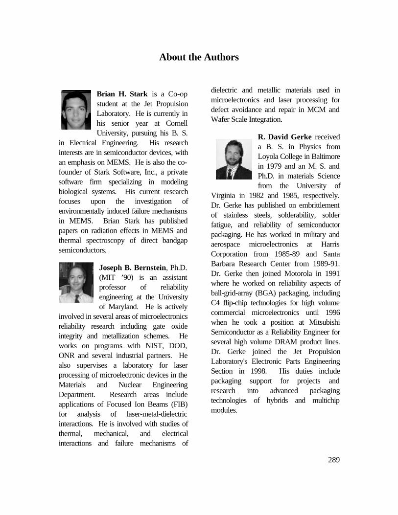
289
About the Authors
Brian H. Stark is a Co-opstudent at the Jet PropulsionLaboratory. He is currently inhis senior year at CornellUniversity, pursuing his B. S.
in Electrical Engineering. His researchinterests are in semiconductor devices, withan emphasis on MEMS. He is also the co-founder of Stark Software, Inc., a privatesoftware firm specializing in modelingbiological systems. His current researchfocuses upon the investigation ofenvironmentally induced failure mechanismsin MEMS. Brian Stark has publishedpapers on radiation effects in MEMS andthermal spectroscopy of direct bandgapsemiconductors.
Joseph B. Bernstein, Ph.D.(MIT ’90) is an assistantprofessor of reliabilityengineering at the Universityof Maryland. He is actively
involved in several areas of microelectronicsreliability research including gate oxideintegrity and metallization schemes. Heworks on programs with NIST, DOD,ONR and several industrial partners. Healso supervises a laboratory for laserprocessing of microelectronic devices in theMaterials and Nuclear EngineeringDepartment. Research areas includeapplications of Focused Ion Beams (FIB)for analysis of laser-metal-dielectricinteractions. He is involved with studies ofthermal, mechanical, and electricalinteractions and failure mechanisms of
dielectric and metallic materials used inmicroelectronics and laser processing fordefect avoidance and repair in MCM andWafer Scale Integration.
R. David Gerke receiveda B. S. in Physics fromLoyola College in Baltimorein 1979 and an M. S. andPh.D. in materials Sciencefrom the University of
Virginia in 1982 and 1985, respectively.Dr. Gerke has published on embrittlementof stainless steels, solderability, solderfatigue, and reliability of semiconductorpackaging. He has worked in military andaerospace microelectronics at HarrisCorporation from 1985-89 and SantaBarbara Research Center from 1989-91.Dr. Gerke then joined Motorola in 1991where he worked on reliability aspects ofball-grid-array (BGA) packaging, includingC4 flip-chip technologies for high volumecommercial microelectronics until 1996when he took a position at MitsubishiSemiconductor as a Reliability Engineer forseveral high volume DRAM product lines.Dr. Gerke joined the Jet PropulsionLaboratory's Electronic Parts EngineeringSection in 1998. His duties includepackaging support for projects andresearch into advanced packagingtechnologies of hybrids and multichipmodules.
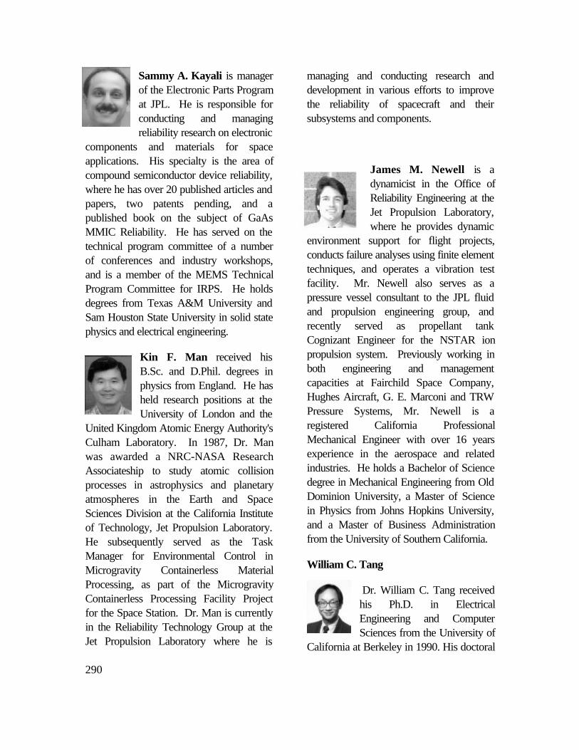
290
Sammy A. Kayali is managerof the Electronic Parts Programat JPL. He is responsible forconducting and managingreliability research on electronic
components and materials for spaceapplications. His specialty is the area ofcompound semiconductor device reliability,where he has over 20 published articles andpapers, two patents pending, and apublished book on the subject of GaAsMMIC Reliability. He has served on thetechnical program committee of a numberof conferences and industry workshops,and is a member of the MEMS TechnicalProgram Committee for IRPS. He holdsdegrees from Texas A&M University andSam Houston State University in solid statephysics and electrical engineering.
Kin F. Man received hisB.Sc. and D.Phil. degrees inphysics from England. He hasheld research positions at theUniversity of London and the
United Kingdom Atomic Energy Authority'sCulham Laboratory. In 1987, Dr. Manwas awarded a NRC-NASA ResearchAssociateship to study atomic collisionprocesses in astrophysics and planetaryatmospheres in the Earth and SpaceSciences Division at the California Instituteof Technology, Jet Propulsion Laboratory.He subsequently served as the TaskManager for Environmental Control inMicrogravity Containerless MaterialProcessing, as part of the MicrogravityContainerless Processing Facility Projectfor the Space Station. Dr. Man is currentlyin the Reliability Technology Group at theJet Propulsion Laboratory where he is
managing and conducting research anddevelopment in various efforts to improvethe reliability of spacecraft and theirsubsystems and components.
James M. Newell is adynamicist in the Office ofReliability Engineering at theJet Propulsion Laboratory,where he provides dynamic
environment support for flight projects,conducts failure analyses using finite elementtechniques, and operates a vibration testfacility. Mr. Newell also serves as apressure vessel consultant to the JPL fluidand propulsion engineering group, andrecently served as propellant tankCognizant Engineer for the NSTAR ionpropulsion system. Previously working inboth engineering and managementcapacities at Fairchild Space Company,Hughes Aircraft, G. E. Marconi and TRWPressure Systems, Mr. Newell is aregistered California ProfessionalMechanical Engineer with over 16 yearsexperience in the aerospace and relatedindustries. He holds a Bachelor of Sciencedegree in Mechanical Engineering from OldDominion University, a Master of Sciencein Physics from Johns Hopkins University,and a Master of Business Administrationfrom the University of Southern California.
William C. Tang
Dr. William C. Tang receivedhis Ph.D. in ElectricalEngineering and ComputerSciences from the University of
California at Berkeley in 1990. His doctoral
291
thesis advisor was Professor Roger T.Howe. He acquired internationalrecognition for his thesis work on surface-micromachined electrostatic comb-driveactuator, on which he holds a U. S. patent.His comb drive invention has become thebasic building block for many importantsurface-micromachined sensor and actuatorresearch programs internationally. Hejoined Ford Research Laboratory inDearborn, Michigan in 1990 as a seniorresearch engineer pursuing research inautomotive applications formicromechanical sensors. In 1993, hebecame the sensor research manager atFord Microelectronics, Inc., in ColoradoSprings, Colorado, managing furtherdevelopment of micromachined automotivesensors and technology transfer tomanufacturing. He championed severalcrucial process development programs thatled to the eventual mass production ofMEMS-fabricated airbag accelerometers.In 1996, he joined JPL, and is currently thesupervisor of the MEMS TechnologyGroup within the Device Research andApplication Section. His current charter isto pursue research and development inmicromachining technology and devices forspace and planetary exploration missions.In addition to the patent on electrostaticcomb-drive actuator, Dr. Tang wasawarded two other U. S. patents onautomotive accelerometers. He is an authoror co-author on over forty conference andrefereed papers in the micromechanics field,and is frequently invited to speak inseminars and workshops. Dr. Tang iscurrently serving on the editorial board forthe Institute of Physics Publishing,
contributing to the Journal ofMicromechanics and Microengineering.