mems based reference oscillator - diva portal20122/fulltext01.pdf · datum date 2005-02-24 språk...
TRANSCRIPT
MEMS based reference oscillator
Master’s thesis in Electronic Devices
by
Joel Hedestig
LITH-ISY-EX--05/3609--SE Linköping 2005


MEMS based reference oscillator
Master’s thesis in Electronic Devices, Department of Electrical Engineering at Linköping Institute of Technology
by
Joel Hedestig
LITH-ISY-EX--05/3609--SE Supervisor: Doctor Cicero S. Vaucher
Department of Integrated Transceivers Philips Research Laboratories Eindhoven
Examiner: Professor Atila Alvandpour
Department of Electrical Engineering Linköping’s University
Linköping 2005-02-24

Avdelning, Institution Division, Department
Institutionen för systemteknik 581 83 LINKÖPING
Datum Date 2005-02-24
Språk Language
Rapporttyp Report category
ISBN
Svenska/Swedish X Engelska/English
Licentiatavhandling X Examensarbete
ISRN LITH-ISY-EX--05/3609--SE
C-uppsats D-uppsats
Serietitel och serienummer Title of series, numbering
ISSN
Övrig rapport ____
URL för elektronisk version http://www.ep.liu.se/exjobb/isy/2005/3609/
Titel Title
MEMS baserad referensoscillator MEMS based reference oscillator
Författare Author
Joel Hedestig
Sammanfattning Abstract The interest in tiny wireless applications raises the demand for an integrated reference oscillator with the same performance as the macroscopic quartz crystal reference oscillators. The main challenge of the thesis is to prove that it is possible to build a MEMS based oscillator that approaches the accuracy level of existing quartz crystal oscillators. The MEMS resonator samples which Philips provides are measured and an equivalent electrical model is designed for them. This model is used in the simulations of the Pierce oscillator and the transresistance amplifier oscillator that are evaluated in this thesis. Finally the Pierce oscillator is implemented in the A BCD2 process and manufactured at Philips Semiconductors in Nijmegen, The Netherlands. A test board, for measuring the Pierce oscillator together with a MEMS resonator or a quartz crystal resonator, is built. The Pierce oscillator is then measured with a quartz crystal resonator. In order to simulate the higher series resistance of the MEMS resonators a resistor is put in series with the quartz crystal. The Pierce oscillator is working with a series resistance of 1 kΩ. With higher series resistance the Pierce oscillator stops working. In circuit simulations the Pierce oscillator is working with a series resistance of about 5 kΩ in the MEMS resonator model. To be sure whether the Pierce oscillator has enough gain for the MEMS resonators, it needs to be measured with them. Temperature variations in the MEMS resonators need to be handled and the phase noise performance of the oscillator must be improved, in order for the MEMS based reference oscillator to be a successful replacement for the quartz crystal reference oscillator.
Nyckelord Keyword MEMS, MEMS-resonator, resonator, oscillator, reference oscillator, quartz crystal


i
Abstract
The interest in tiny wireless applications raises the demand for an integrated reference oscillator with the same performance as the macroscopic quartz crystal reference oscillators. The main challenge of the thesis is to prove that it is possible to build a MEMS based oscillator that approaches the accuracy level of existing quartz crystal oscillators.
The MEMS-resonator samples which Philips provides are measured and an equivalent electrical model is designed for them. This model is used in the simulations of the Pierce oscillator and the transresistance amplifier oscillator that are evaluated in this thesis. Finally the Pierce oscillator is implemented in the A-BCD2 process and manufactured at Philips Semiconductors in Nijmegen, The Netherlands. A test board, for measuring the Pierce oscillator together with a MEMS-resonator or a quartz crystal resonator, is built.
The Pierce oscillator is then measured with a quartz crystal resonator. In order to simulate the higher series resistance of the MEMS-resonators a resistor is put in series with the quartz crystal. The Pierce oscillator is working with a series resistance of 1 kΩ. With higher series resistance the Pierce oscillator stops working. In circuit simulations the Pierce oscillator is working with a series resistance of about 5 kΩ in the MEMS-resonator model. To be sure whether the Pierce oscillator has enough gain for the MEMS-resonators, it needs to be measured with them.
Temperature variations in the MEMS-resonators need to be handled and the phase noise performance of the oscillator must be improved, in order for the MEMS based reference oscillator to be a successful replacement for the quartz crystal reference oscillator.


iii
Preface
This report is the result of a Master’s thesis carried out during an internship at Philips Research in Eindhoven, The Netherlands, starting off in September 2004 and ending in the middle of February 2005.
The purpose of this thesis has been to prove that it is possible to build a MEMS based oscillator that approaches the accuracy level of existing quartz crystal oscillators. In the beginning of the internship several MEMS-resonator samples were available for characterization. The idea was to use a model of one of these MEMS-resonators and design an oscillator circuit around it. The target was a reference oscillator that approaches the phase noise and frequency stability demands of the GSM specification.
It is the recent interest in tiny and ultra thin wireless applications that have raised the efforts to integrate off-chip passive devices needed for frequency generation in wireless communication circuits. Examples of this kind of applications are credit-card sized wireless devices and wireless microsensors.


v
Acknowledgements
This Master’s thesis was written during an internship at Philips Research in Eindhoven, The Netherlands. It has been an inspiring and educational time for me to be working in one of the world’s larges research centers, which indeed has a lot of benefits. During my time at Philips Research I found it interesting to see how research projects are run and to attend the project meetings at Philips Semiconductors in Nijmegen, which has given me insight into the business. When needed, it has been possible to find experts within different areas, providing help with difficult parts of my project.
Among the employees at Philips I would specially like to thank my supervisor, Dr. Cicero S. Vaucher, who has taught me a lot and supported me greatly. Ir. Joost van Beek and Dr. Peter G. Steeneken, who helped me understand, measure and build the electrical model of the MEMS-resonators. Dr. Jan-Jaap Koning, who provided me with information about the A-BCD2 process and helped me at tape-out. At Linköping’s University I would like to thank my supervisor, Professor Atila Alvandpour, for all his support and feedback.
I would like to thank all my fellow students here at Philips High-Tech Campus, especially my companions and very good friends Goran Jerin and Samir Jašarević, for all the good laughs and wonderful times together. I would like to thank my brother John Hedestig for all the feedback on my report. At last but not at least, I would like to thank the love of my life, my fiancée Therese Hedlund, who put up with our long time apart and supported me during my stay in Eindhoven. I would also like to thank her for all the valuable feedback on my report.


vii
Contents
Abstract............................................................................................................................... i
Preface............................................................................................................................... iii
Acknowledgements ........................................................................................................... v
Chapter 1 Introduction..................................................................................... 1
1.1 Presentation of Royal Philips Electronics of the Netherlands ............................ 2 1.2 RF MEMS........................................................................................................... 2
1.2.1 Definition of MEMS-resonator................................................................... 2 1.2.2 MEMS-resonator theory ............................................................................. 2 1.2.3 A resonator’s equivalent electrical circuit .................................................. 4 1.2.4 Quality factor .............................................................................................. 4 1.2.5 Clamped-clamped beam resonator.............................................................. 5
Chapter 2 Characterization and electrical model .......................................... 7
2.1 Measurement setup ............................................................................................. 7 2.2 Equivalent electrical circuit of the clamped-clamped beam resonator ............... 9
Chapter 3 Oscillator circuit ........................................................................... 15
3.1 Basic resonator circuit connection .................................................................... 16 3.2 Resonator response to a step input.................................................................... 17 3.3 Pierce oscillator circuit ..................................................................................... 19
3.3.1 Detailed circuit schematic......................................................................... 20 3.3.2 Open-loop analysis.................................................................................... 21
3.4 Transresistance amplifier oscillator .................................................................. 22 3.4.1 Detailed circuit schematic......................................................................... 23

_______________________________________________________________________
viii
3.4.2 Open-loop analysis.................................................................................... 27
Chapter 4 Layout ............................................................................................ 31
4.1 A-BCD2 process ............................................................................................... 31 4.1.1 SOI technology ......................................................................................... 32
4.2 Pierce oscillator layout...................................................................................... 32 4.3 Transresistance amplifier oscillator layout ....................................................... 32 4.4 Final chip layout ............................................................................................... 33
Chapter 5 Final measurements...................................................................... 37
5.1 Test board.......................................................................................................... 37 5.2 Measurement..................................................................................................... 39
Chapter 6 Conclusion ..................................................................................... 41
6.1 Future work....................................................................................................... 42 6.1.1 Automatic level control............................................................................. 42 6.1.2 Compensating for temperature variations................................................. 42 6.1.3 Integrating resonator and circuit on same chip ......................................... 42 6.1.4 Frequency calibration................................................................................ 42
Appendix A ADS optimization setup................................................................ 45
A.1 Measurement setup 1 ........................................................................................ 46 A.2 Measurement setup 2 ........................................................................................ 47 A.3 Measurement setup 3 ........................................................................................ 48
Appendix B Open-loop analysis........................................................................ 49
B.1 Open-loop analysis tool .................................................................................... 50 B.2 Simulation setup for the Pierce oscillator ......................................................... 51 B.3 Simulation setup for transresistance amplifier oscillator.................................. 52
Appendix C Shunt-shunt feedback ................................................................... 53
Appendix D MEMS-resonators......................................................................... 55 D.1 Temperature stability ........................................................................................ 56 D.2 DC voltage influence on resonance frequency ................................................. 57 D.3 Input power influence on resonance frequency ................................................ 58 D.4 Compensating for temperature variations......................................................... 58
References........................................................................................................................ 59
1
Chapter 1 Introduction
In recent years, the interest in tiny wireless applications has fueled efforts to flatten the form factors of the off-chip passive devices needed for frequency generation in wireless communication circuits. The quartz crystal, used in reference oscillators, is perhaps the most difficult to miniaturize and integrate on chip, since on-chip devices capable of matching its frequency stability have so far been unavailable.
Recent efforts to integrate reference oscillators have focused on MEMS-resonators as potential replacements for the high Q and temperature stable quartz crystals. Several promising MEMS-resonators have been tested in recent years. Oscillators based on these MEMS-resonators have been demonstrated, but very few of these is meeting the GSM reference oscillator phase noise performance specification of –130 dBc/Hz at 1 kHz offset from a 13 MHz carrier and –150 dBc/Hz at far-from-carrier offsets and none of these oscillators come close to the required temperature dependence specifications of less than 35 ppm (2 ppm after compensation) total frequency shift from 0°C to 70°C.
Theoretically, the short-term stability of MEMS based oscillators are sufficient to satisfy the needs of reference oscillators, but their temperature stability falls well short of the marks required by oscillators. Several different techniques for handling the temperature instability have been investigated.
The main challenge of the thesis is to prove that it is possible to build a MEMS based oscillator that approaches the accuracy level of existing quartz crystal oscillators. In this work the MEMS-resonators provided by Philips are measured and characterized and an equivalent electrical circuit of them is designed. This equivalent electrical circuit is used in the simulations of the different oscillator circuits evaluated in this work. The focus will be on two circuits, the Pierce oscillator and the transresistance amplifier oscillator. The Pierce oscillator is implemented on a chip, which is manufactured at Philips
Chapter 1 Introduction _______________________________________________________________________
2
Semiconductors. For this chip, a test board is designed and built, which is used for measuring and evaluating the Pierce oscillator chip.
This first chapter covers the basic theory behind MEMS-resonators. The clamped-clamped beam MEMS-resonator, used in this work, is presented in this chapter.
1.1 Presentation of Royal Philips Electronics of the Netherlands Royal Philips Electronics of the Netherlands is one of the world's biggest electronics companies and Europe's largest, with sales of EUR 30.3 billion in 2004. Philips has activities in the three interlocking domains of healthcare, lifestyle and technology and 161 500 employees in more than 60 countries. It has market leadership positions in medical diagnostic imaging and patient monitoring, color television sets, electric shavers, lighting and silicon system solutions. Philips Research has laboratories in five different countries The Netherlands, England, Germany, China and the United States, and is staffed by around 2 100 people. The activities by Philips Research have lead to over 100 000 patents and design rights, and the publishing of many thousands of technical and scientific papers. The annual research budget is slightly less than 1% of Philips Electronics annual sales.
1.2 RF MEMS MEMS is the abbreviation for micro-electromechanical-system. As the name indicates, it is a device in the size of microns, controllable with electrical signals and it contains moving parts.
1.2.1 Definition of MEMS-resonator A MEMS-resonator is a device of several tens of microns. By applying electrostatic forces and an AC current to it, the component will resonate. A MEMS-resonator consists of a free moving part without contact to anything except for its anchors. This free element can vibrate and is often a free beam, but it can also be a square, a disk or a much more complex structure [7], [10], [23], [24], [26], [27].
A MEMS-resonator is coupled electromechanically. This means that there is a relation between the input current and the mechanical behavior of the resonator, i.e. the resonance of the vibrating element. The free element will oscillate with the frequency of the input current and when the frequency is equal to one of the resonance frequency modes of the element, it will enter resonance. Several ways of coupling exist, piezoresistive, piezoelectric, optical and capacitive actuation and detection. Capacitive actuation and detection is the most used coupling method. The MEMS-resonator is characterized by its resonance frequency and quality factor (Q-factor). [3]
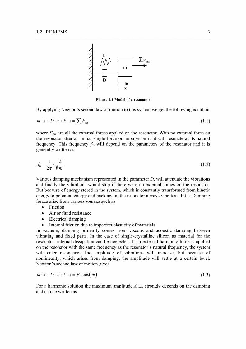
1.2.2 MEMS-resonator theory In order to understand the mechanical behavior of a MEMS-resonator, a simple model of it is made. The resonator model consists of a free mass that is connected to the ground by a spring and a damper, as show in Figure 1.1. The mass m, spring constant k, and damping coefficient D, depends on the design and the properties of the resonator. Most important are the Young modulus, the density and the dimensions of the resonator.
1.2 RF MEMS _______________________________________________________________________
3
m
x
k
D
ΣFext
Figure 1.1 Model of a resonator
By applying Newton’s second law of motion to this system we get the following equation
∑=⋅+⋅+⋅ extFxkxDxm &&& (1.1)
where Fext are all the external forces applied on the resonator. With no external force on the resonator after an initial single force or impulse on it, it will resonate at its natural frequency. This frequency f0, will depend on the parameters of the resonator and it is generally written as
mkf ⋅=
π21
0 (1.2)
Various damping mechanism represented in the parameter D, will attenuate the vibrations and finally the vibrations would stop if there were no external forces on the resonator. But because of energy stored in the system, which is constantly transformed from kinetic energy to potential energy and back again, the resonator always vibrates a little. Damping forces arise from various sources such as:
• Friction • Air or fluid resistance • Electrical damping • Internal friction due to imperfect elasticity of materials
In vacuum, damping primarily comes from viscous and acoustic damping between vibrating and fixed parts. In the case of single-crystalline silicon as material for the resonator, internal dissipation can be neglected. If an external harmonic force is applied on the resonator with the same frequency as the resonator’s natural frequency, the system will enter resonance. The amplitude of vibrations will increase, but because of nonlinearity, which arises from damping, the amplitude will settle at a certain level. Newton’s second law of motion gives
( )tFxkxDxm ωcos⋅=⋅+⋅+⋅ &&& (1.3)
For a harmonic solution the maximum amplitude Amax, strongly depends on the damping and can be written as

Chapter 1 Introduction _______________________________________________________________________
4
km
DF
Dmkm
DFA ⋅≅
−⋅
⋅=
41
2
2max for small damping, D (1.4)
From (1.4) we can draw the conclusion that for a large damping, Amax does not exist, and therefore no resonance exists. On the contrary, for a small damping the maximum amplitude becomes very large. [3]
The design of a resonator equivalent electrical circuit is based on the differential equation of the resonator’s mechanical model.
1.2.3 A resonator’s equivalent electrical circuit The equivalent circuit using lumped constant elements for a resonator is shown in Figure 1.2. All resonators can be modeled in this way. The inductance Lx and the capacitance Cx represent the resonator’s frequency sensitive elements [1], [2]. Compared to a quartz crystal resonator the series resistance Rs of the MEMS-resonator is large. This will impose a problem when designing the oscillator circuit, because the amplifier in the oscillator circuit will need a large gain to fulfill the oscillation condition and an even larger gain to get a fast startup time. This problem will be discussed further in Chapter 3. The equivalent circuit is based on the analogy of the mathematical description for the electrical and mechanical phenomena. These two phenomena have similar differential equations (1.1), and it is only these similarities that allow this equivalent electrical circuit [3]. The lumped elements values Rs and Cx can be used for calculating the resonator’s quality factor Q.
Figure 1.2 A resonator’s equivalent electrical circuit
1.2.4 Quality factor The Quality factor or Q-factor is an important parameter of a MEMS-resonator. Resonators with high Q-factors are frequency stable and give low phase-noise in oscillators. According to [3], for a resonator, the Q-factor is defined as:
( )( )resonanceofcycleperdissipatedenergy
devicetheinstoredenergyQ = (1.5)
The frequency at the maximum magnitude of the gain curve is used as the resonance frequency, f0, and the half power points (-3dB) are determined on either side of the
1.2 RF MEMS _______________________________________________________________________
5
resonance frequency and the difference of those frequency positions is the bandwidth, ∆f3dB. Then the Q-factor can be defined as:
dBffQ3
0
∆= (1.6)
According to [28], this is also the definition of the loaded quality factor Ql of an oscillator circuit. For discrete data this definition can give poor results. For more reliable value of Q-factor it is better to fit a curve to the discrete data and calculate the Q-factor from the fitted curve. [4]
A curve fit (for example, a curve fitted to S-parameter data from measurements made on a resonator) will give the values of the resonator’s series resistance Rs and motional capacitance Cx. These two values and the following definition of the Q-factor:
sxRCfQ
021
π= (1.7)
where f0 is the resonance frequency, will give an accurate value on the Q-factor.
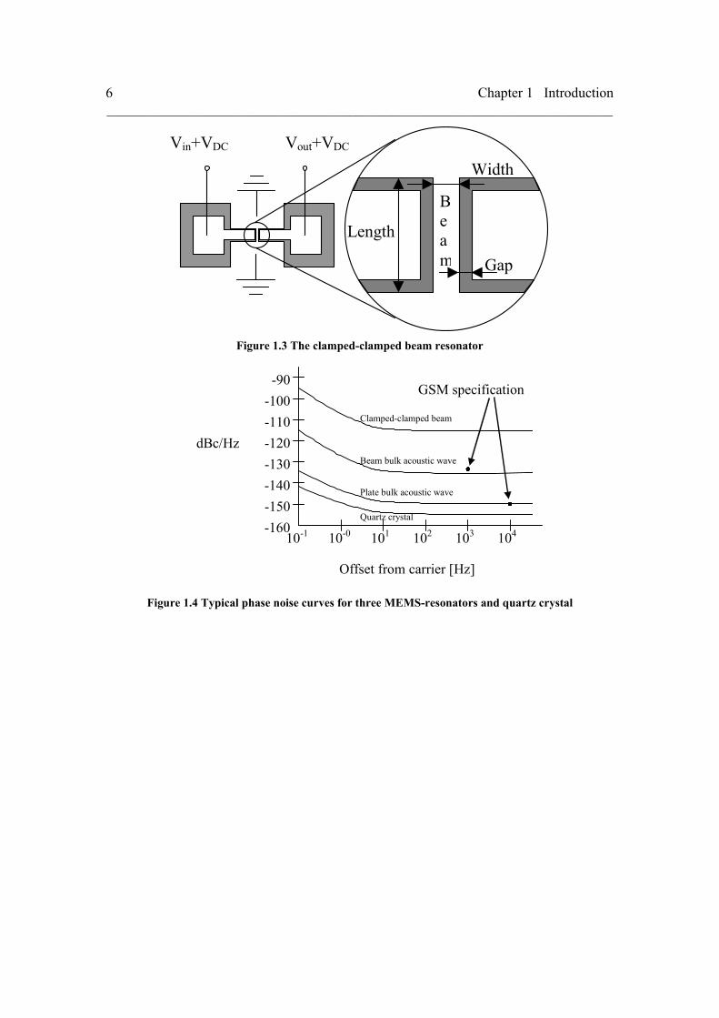
1.2.5 Clamped-clamped beam resonator The clamped-clamped beam resonator is constructed of a beam that is clamped at its both ends, as shown in Figure 1.3. The resonance frequency of the beam is depending on the dimensions of the beam (length and width), and the material properties (Young modulus and density) [3]. On each of the two electrodes a DC voltage is applied. DC voltage is needed to get the correct electrostatic force between the electrodes and the beam. Without DC voltage, the beam will resonate at double frequency and also there will not be an output signal. Hence it is important to have the DC voltage.
In addition to the DC voltage an AC signal Vin, is applied to one of the electrodes. To enter resonance, the AC signal Vin, must have the same frequency as the resonance frequency of the beam. The output is taken from the other electrode. The oscillator will be designed around a model of the clamped-clamped beam resonator. This is the resonator type that is available for measurements and characterization.
By using the clamped-clamped beam resonator, we know from theory that it will not meet the requirements of the GSM specification, as shown in [7] and Figure 1.4. The stringent GSM specification requires a phase noise-to-carrier density ratio of -130 dBc/Hz at 1 kHz offset from a 13 MHz carrier, and –150 dBc/Hz at far-from-carrier offsets. Phase noise is the measure of the short-term frequency instability of an oscillator. It is measured as the single sideband noise, resulting from changes in frequency, in decibels below the amplitude at the operating frequency of the oscillator using a 1 Hz bandwidth (dBc/Hz) at two or more frequency displacements from the operating frequency of an oscillator. Even though the clamped-clamped beam resonator does not fulfill the GSM specification, it is still a good model to design the oscillator around. In order to use the clamped-clamped beam resonator in circuit simulations, an equivalent electrical model of it is needed.
Chapter 1 Introduction _______________________________________________________________________
6
Vin+VDC Vout+VDC
Gap
Width
Length
Beam
Figure 1.3 The clamped-clamped beam resonator
-160 -150 -140 -130 -120 -110 -100
-90
dBc/Hz
10-1 10-0 101 102 103 104
Offset from carrier [Hz]
Clamped-clamped beam
Beam bulk acoustic wave
Plate bulk acoustic wave
Quartz crystal
GSM specification
Figure 1.4 Typical phase noise curves for three MEMS-resonators and quartz crystal
7
Chapter 2 Characterization and electrical model
In this chapter the characterization of the MEMS-resonator is discussed. Three different equivalent electrical circuits of the clamped-clamped beam resonator are tested. The equivalent electrical circuits are fitted to an S12-parameter curve, with the software Advanced Design System or ADS. The S-parameters are taken from measurements made on a clamped-clamped beam resonator inside a vacuum chamber.
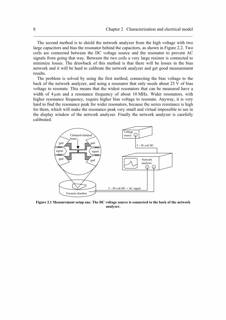
2.1 Measurement setup The MEMS-resonators are measured with a HP 8753 D network analyzer. Since it is difficult to measure total current and voltage at higher frequencies, the network analyzer measures the S-parameters instead. These parameters relate to familiar quantities such as gain, loss and reflection coefficients and they can easily be converted to Z-parameters, Y-parameters or H-parameters. The resonator is put inside a vacuum chamber to minimize damping effects. Without vacuum the resonator will be impossible to measure, because the damping from the surrounding air will be too large and there will be no resonance.
To get the needed electrostatic force between the beam and the electrode of the resonator, it is biased with a DC voltage ranging from 5 V up to 100 V depending on the dimensions of the resonator. There are two ways of doing this. The first possibility is to connect a DC voltage source to the back of the network analyzer, as shown in Figure 2.1. The drawback of this method is that the network analyzer can only handle a maximum voltage of 30 V.
Chapter 2 Characterization and electrical model _______________________________________________________________________
8
The second method is to shield the network analyzer from the high voltage with two large capacitors and bias the resonator behind the capacitors, as shown in Figure 2.2. Two coils are connected between the DC voltage source and the resonator to prevent AC signals from going that way. Between the two coils a very large resistor is connected to minimize losses. The drawback of this method is that there will be losses in the bias network and it will be hard to calibrate the network analyzer and get good measurement results.
The problem is solved by using the first method, connecting the bias voltage to the back of the network analyzer, and using a resonator that only needs about 25 V of bias voltage to resonate. This means that the widest resonators that can be measured have a width of 4 µm and a resonance frequency of about 10 MHz. Wider resonators, with higher resonance frequency, require higher bias voltage to resonate. Anyway, it is very hard to find the resonance peak for wider resonators, because the series resistance is high for them, which will make the resonance peak very small and virtual impossible to see in the display window of the network analyzer. Finally the network analyzer is carefully calibrated.
Vacuum chamber
Network analyzer
Voltagesource
5 - 30 volt DC
5 - 30 volt DC + AC signal
Clamped-clamped beam
signal
gnd
gnd
gnd
signal
gnd
Figure 2.1 Measurement setup one. The DC voltage source is connected to the back of the network
analyzer.

2.2 Equivalent electrical circuit of the clamped-clamped beam resonator _______________________________________________________________________
9
Vacuum chamber
Network analyzer
Voltagesource Clamped-clamped
beam
5 - 100 volt DC
5 - 100 volt DC + AC signal
1 MΩ gnd
signal
gnd
signal
gnd
gnd
Figure 2.2 Measurement setup two. The network analyzer is shielded from the high voltage with two
large capacitors.
2.2 Equivalent electrical circuit of the clamped-clamped beam resonator
In this study, three different equivalent circuits for the clamped-clamped beam resonator are tested. All circuits are fitted to the S12 parameter curve from measurements made on a resonator with gap = 0.3 µm, width = 4 µm and a resonance frequency of about 9.922 MHz. The DC bias voltage for this measurement is set to 27.5 V. This setup gives the nicest measurement result. The first one and the most well know is the circuit shown in Figure 2.3. It is described in [1], [2], [13]. It is the same equivalent circuit that is used to model the quartz crystal resonator. For the quartz crystal resonator, the working capacitance Cp is the capacitance between the metallized electrodes on both sides of the crystal. For the clamped-clamped beam resonator, the working capacitance Cp is caused by the air gap separating the electrodes from the beam.
This is not a completely true model in physical perspective, which will be shown later. This model is tested because it is simple and well known from quartz crystal theory. To find the electrical values, Lx, Cx and Rs, the circuit is fitted to measured data in the software tool Advanced Design System or ADS. It is not a good fit, as shown in Figure 2.4. There is no parallel resonance in the measurement and there is also an offset in the signal floor. This fit gives the values Rs = 4.69 kΩ, Cx = 318 aF, Lx = 809 mH and Cp = 242 fF.
Figure 2.3 First equivalent electrical circuit of the clamped-clamped beam resonator

Chapter 2 Characterization and electrical model _______________________________________________________________________
10
Figure 2.4 S12-parameter plot of equivalent electrical circuit fitted to measured data. The solid line is
measured data and the dashed line is the fitted curve. This fit gives the values Rs = 4.69 kΩ, Cx = 318 aF, Lx = 809 mH and Cp = 242 fF.
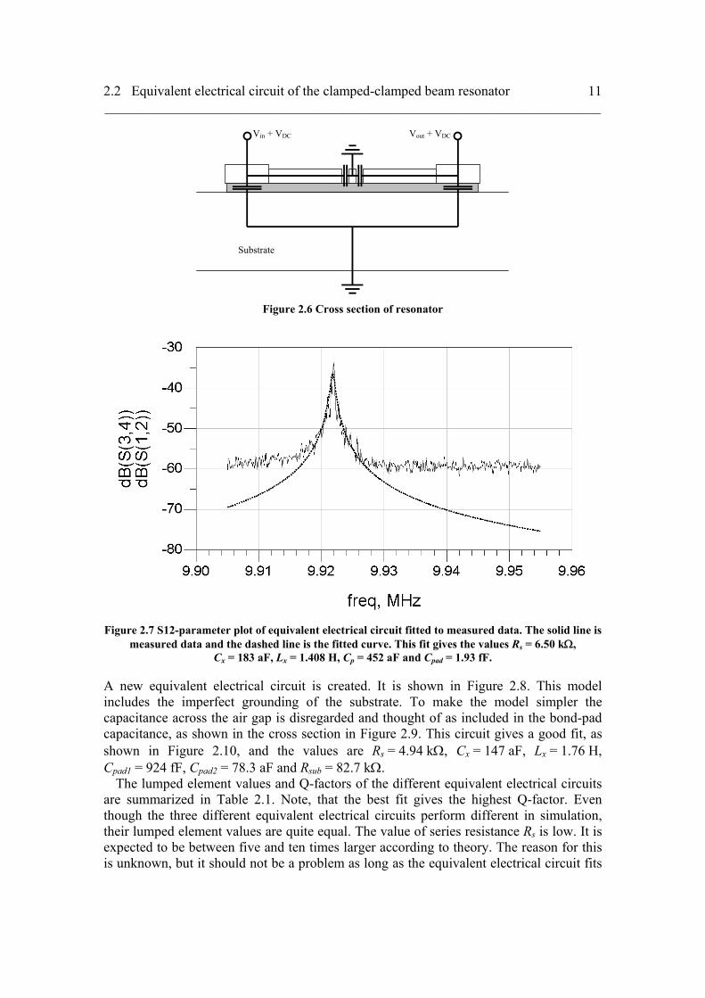
To find a better fit the equivalent circuit in [3] is tested. This circuit is shown in Figure 2.5 and a cross section of the resonator is shown in Figure 2.6. The resonator’s beam is grounded and placed between two working capacitances Cp. As before the capacitance Cp is caused by the air gap between the electrodes and the beam. Two parasitic capacitances are added from the bond-pads to the electrodes. This model is closer to the truth. The fitted curve is shown in Figure 2.7. The circuit fits the measurement very well close to the resonance frequency, but further away from it the fit is bad. The problem with this model is that in reality the substrate is not perfectly grounded. This fit gives the values Rs = 6.50 kΩ, Cx = 183 aF, Lx = 1.408 H, Cp = 452 aF and Cpad = 1.93 fF.
Figure 2.5 Second equivalent electrical circuit of the clamped-clamped beam resonator
2.2 Equivalent electrical circuit of the clamped-clamped beam resonator _______________________________________________________________________
11
Substrate
Vin + VDC Vout + VDC
Figure 2.6 Cross section of resonator
Figure 2.7 S12-parameter plot of equivalent electrical circuit fitted to measured data. The solid line is
measured data and the dashed line is the fitted curve. This fit gives the values Rs = 6.50 kΩ, Cx = 183 aF, Lx = 1.408 H, Cp = 452 aF and Cpad = 1.93 fF.
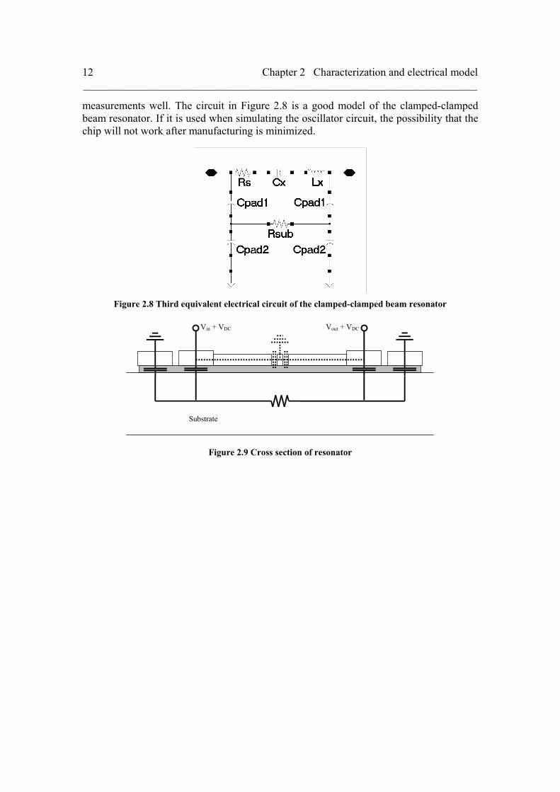
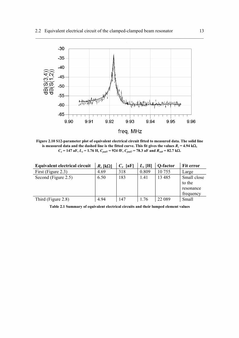
A new equivalent electrical circuit is created. It is shown in Figure 2.8. This model includes the imperfect grounding of the substrate. To make the model simpler the capacitance across the air gap is disregarded and thought of as included in the bond-pad capacitance, as shown in the cross section in Figure 2.9. This circuit gives a good fit, as shown in Figure 2.10, and the values are Rs = 4.94 kΩ, Cx = 147 aF, Lx = 1.76 H, Cpad1 = 924 fF, Cpad2 = 78.3 aF and Rsub = 82.7 kΩ.
The lumped element values and Q-factors of the different equivalent electrical circuits are summarized in Table 2.1. Note, that the best fit gives the highest Q-factor. Even though the three different equivalent electrical circuits perform different in simulation, their lumped element values are quite equal. The value of series resistance Rs is low. It is expected to be between five and ten times larger according to theory. The reason for this is unknown, but it should not be a problem as long as the equivalent electrical circuit fits
Chapter 2 Characterization and electrical model _______________________________________________________________________
12
measurements well. The circuit in Figure 2.8 is a good model of the clamped-clamped beam resonator. If it is used when simulating the oscillator circuit, the possibility that the chip will not work after manufacturing is minimized.
Figure 2.8 Third equivalent electrical circuit of the clamped-clamped beam resonator
Substrate
Vin + VDC Vout + VDC
Figure 2.9 Cross section of resonator
2.2 Equivalent electrical circuit of the clamped-clamped beam resonator _______________________________________________________________________
13
Figure 2.10 S12-parameter plot of equivalent electrical circuit fitted to measured data. The solid line
is measured data and the dashed line is the fitted curve. This fit gives the values Rs = 4.94 kΩ, Cx = 147 aF, Lx = 1.76 H, Cpad1 = 924 fF, Cpad2 = 78.3 aF and Rsub = 82.7 kΩ.
Equivalent electrical circuit Rs [kΩ] Cx [aF] Lx [H] Q-factor Fit error First (Figure 2.3) 4.69 318 0.809 10 755 Large Second (Figure 2.5) 6.50 183 1.41 13 485 Small close
to the resonance frequency
Third (Figure 2.8) 4.94 147 1.76 22 089 Small Table 2.1 Summary of equivalent electrical circuits and their lumped element values

15
Chapter 3 Oscillator circuit
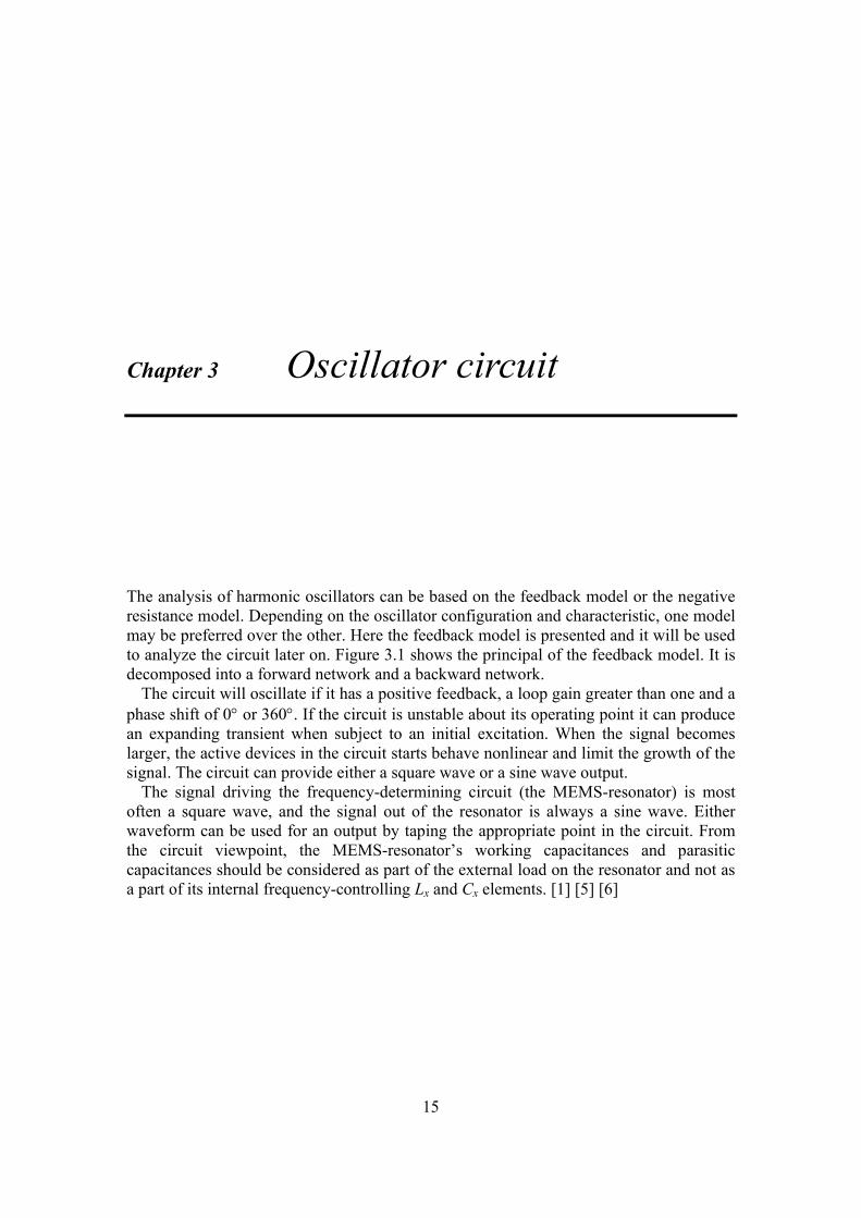
The analysis of harmonic oscillators can be based on the feedback model or the negative resistance model. Depending on the oscillator configuration and characteristic, one model may be preferred over the other. Here the feedback model is presented and it will be used to analyze the circuit later on. Figure 3.1 shows the principal of the feedback model. It is decomposed into a forward network and a backward network.
The circuit will oscillate if it has a positive feedback, a loop gain greater than one and a phase shift of 0° or 360°. If the circuit is unstable about its operating point it can produce an expanding transient when subject to an initial excitation. When the signal becomes larger, the active devices in the circuit starts behave nonlinear and limit the growth of the signal. The circuit can provide either a square wave or a sine wave output.
The signal driving the frequency-determining circuit (the MEMS-resonator) is most often a square wave, and the signal out of the resonator is always a sine wave. Either waveform can be used for an output by taping the appropriate point in the circuit. From the circuit viewpoint, the MEMS-resonator’s working capacitances and parasitic capacitances should be considered as part of the external load on the resonator and not as a part of its internal frequency-controlling Lx and Cx elements. [1] [5] [6]
Chapter 3 Oscillator circuit _______________________________________________________________________
16
Feedback network
f(s)
Forward network
a(s)
Figure 3.1 Feedback model
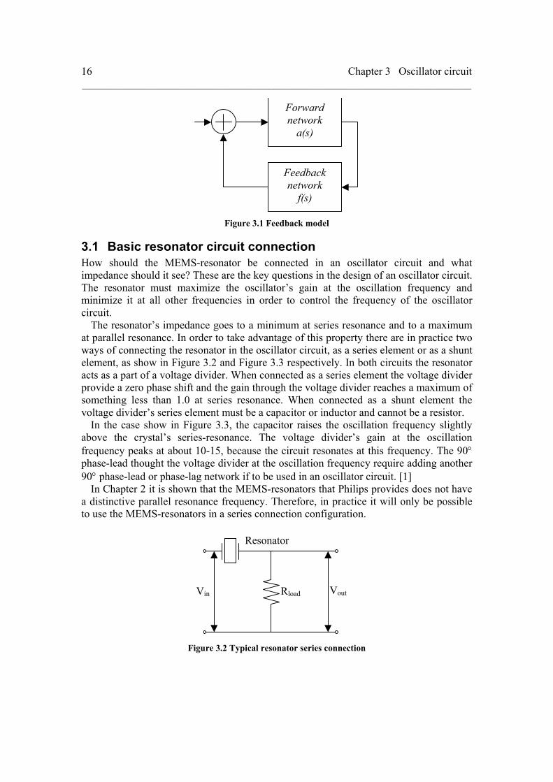
3.1 Basic resonator circuit connection How should the MEMS-resonator be connected in an oscillator circuit and what impedance should it see? These are the key questions in the design of an oscillator circuit. The resonator must maximize the oscillator’s gain at the oscillation frequency and minimize it at all other frequencies in order to control the frequency of the oscillator circuit.
The resonator’s impedance goes to a minimum at series resonance and to a maximum at parallel resonance. In order to take advantage of this property there are in practice two ways of connecting the resonator in the oscillator circuit, as a series element or as a shunt element, as show in Figure 3.2 and Figure 3.3 respectively. In both circuits the resonator acts as a part of a voltage divider. When connected as a series element the voltage divider provide a zero phase shift and the gain through the voltage divider reaches a maximum of something less than 1.0 at series resonance. When connected as a shunt element the voltage divider’s series element must be a capacitor or inductor and cannot be a resistor.
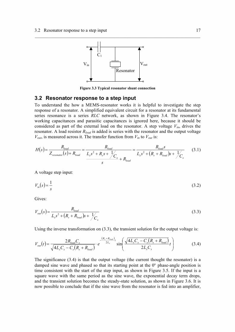
In the case show in Figure 3.3, the capacitor raises the oscillation frequency slightly above the crystal’s series-resonance. The voltage divider’s gain at the oscillation frequency peaks at about 10-15, because the circuit resonates at this frequency. The 90° phase-lead thought the voltage divider at the oscillation frequency require adding another 90° phase-lead or phase-lag network if to be used in an oscillator circuit. [1]
In Chapter 2 it is shown that the MEMS-resonators that Philips provides does not have a distinctive parallel resonance frequency. Therefore, in practice it will only be possible to use the MEMS-resonators in a series connection configuration.
Vin Vout Rload
Resonator
Figure 3.2 Typical resonator series connection
3.2 Resonator response to a step input _______________________________________________________________________
17
Vin Vout
C1
Resonator
Figure 3.3 Typical resonator shunt connection
3.2 Resonator response to a step input To understand the how a MEMS-resonator works it is helpful to investigate the step response of a resonator. A simplified equivalent circuit for a resonator at its fundamental series resonance is a series RLC network, as shown in Figure 3.4. The resonator’s working capacitances and parasitic capacitances is ignored here, because it should be considered as part of the external load on the resonator. A step voltage Vin, drives the resonator. A load resistor Rload is added is series with the resonator and the output voltage Vout, is measured across it. The transfer function from Vin to Vout is:
( ) ( ) ( )x
loadsx
load
loadx
sx
load
loadresonator
load
CsRRsLsR
Rs
CsRsLR
RsZRsH 11 22 +++
=
+++
=+
= (3.1)
A voltage step input:
( )s
sVin1
= (3.2)
Gives:
( )( )
xloadsx
loadout
CsRRsLRsV 12 +++
= (3.3)
Using the inverse transformation on (3.3), the transient solution for the output voltage is:
( )( )
( ) ( )⎟⎟⎠
⎞⎜⎜⎝
⎛ +−⋅
+−=
+−
tCL
RRCCLe
RRCCLCRtV
xx
loadsxxxt
LRR
loadsxxx
xloadout
x
loads
24
sin4
2 2 (3.4)
The significance (3.4) is that the output voltage (the current thought the resonator) is a damped sine wave and phased so that its starting point at the 0° phase-angle position is time consistent with the start of the step input, as shown in Figure 3.5. If the input is a square wave with the same period as the sine wave, the exponential decay term drops, and the transient solution becomes the steady-state solution, as shown in Figure 3.6. It is now possible to conclude that if the sine wave from the resonator is fed into an amplifier,

Chapter 3 Oscillator circuit _______________________________________________________________________
18
with enough gain, and the output of the amplifier is used to drive the resonator, there is continuous oscillation in the resonator. [1]
Figure 3.4 Simplified equivalent circuit of the resonator
Figure 3.5 Resonator response to a step input
Figure 3.6 Resonator response to a square wave drive
3.3 Pierce oscillator circuit _______________________________________________________________________
19
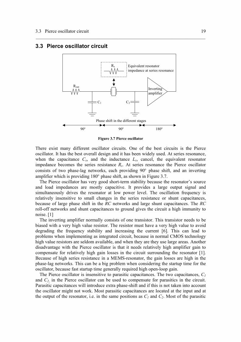
3.3 Pierce oscillator circuit
90° 90° 180°
Equivalent resonator impedance at series resonance
Rs
Phase shift in the different stages
Inverting amplifier
C1 C2
Rout
Figure 3.7 Pierce oscillator
There exist many different oscillator circuits. One of the best circuits is the Pierce oscillator. It has the best overall design and it has been widely used. At series resonance, when the capacitance Cx, and the inductance Lx, cancel, the equivalent resonator impedance becomes the series resistance Rs. At series resonance the Pierce oscillator consists of two phase-lag networks, each providing 90° phase shift, and an inverting amplifier which is providing 180° phase shift, as shown in Figure 3.7.
The Pierce oscillator has very good short-term stability because the resonator’s source and load impedances are mostly capacitive. It provides a large output signal and simultaneously drives the resonator at low power level. The oscillation frequency is relatively insensitive to small changes in the series resistance or shunt capacitances, because of large phase shift in the RC networks and large shunt capacitances. The RC roll-off networks and shunt capacitances to ground gives the circuit a high immunity to noise. [1]
The inverting amplifier normally consists of one transistor. This transistor needs to be biased with a very high value resistor. The resistor must have a very high value to avoid degrading the frequency stability and increasing the current [6]. This can lead to problems when implementing as integrated circuit, because in normal CMOS technology high value resistors are seldom available, and when they are they use large areas. Another disadvantage with the Pierce oscillator is that it needs relatively high amplifier gain to compensate for relatively high gain losses in the circuit surrounding the resonator [1]. Because of high series resistance in a MEMS-resonator, the gain losses are high in the phase-lag networks. This can be a big problem when considering the startup time for the oscillator, because fast startup time generally required high open-loop gain.
The Pierce oscillator is insensitive to parasitic capacitances. The two capacitances, C1 and C2, in the Pierce oscillator can be used to compensate for parasitics in the circuit. Parasitic capacitances will introduce extra phase-shift and if this is not taken into account the oscillator might not work. Most parasitic capacitances are located at the input and at the output of the resonator, i.e. in the same positions as C1 and C2. Most of the parasitic
Chapter 3 Oscillator circuit _______________________________________________________________________
20
capacitance comes from the transistors in the amplifier, bond-pads, bond-wires, parasitics in the resonator and the resonator’s bias circuit. To compensate for the parasitic capacitances, C1 and C2 are made smaller.
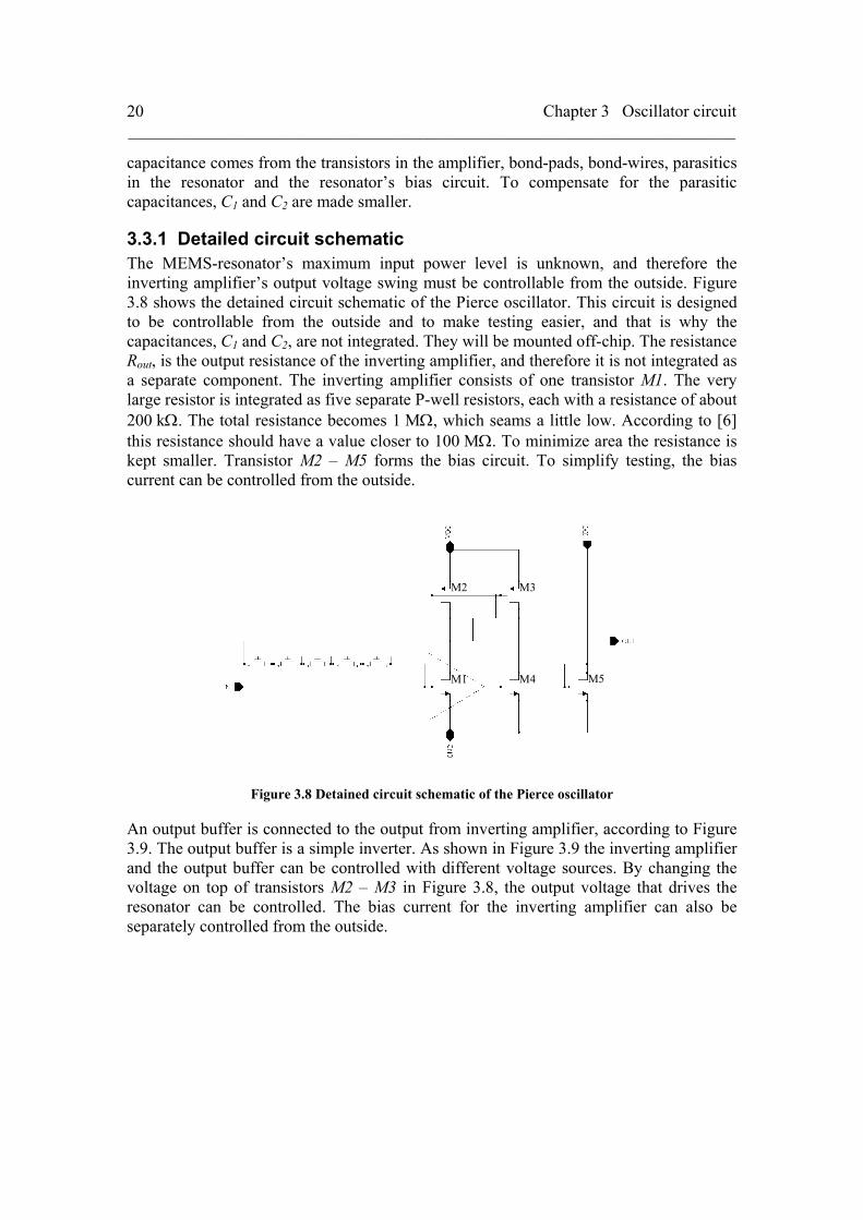
3.3.1 Detailed circuit schematic The MEMS-resonator’s maximum input power level is unknown, and therefore the inverting amplifier’s output voltage swing must be controllable from the outside. Figure 3.8 shows the detained circuit schematic of the Pierce oscillator. This circuit is designed to be controllable from the outside and to make testing easier, and that is why the capacitances, C1 and C2, are not integrated. They will be mounted off-chip. The resistance Rout, is the output resistance of the inverting amplifier, and therefore it is not integrated as a separate component. The inverting amplifier consists of one transistor M1. The very large resistor is integrated as five separate P-well resistors, each with a resistance of about 200 kΩ. The total resistance becomes 1 MΩ, which seams a little low. According to [6] this resistance should have a value closer to 100 MΩ. To minimize area the resistance is kept smaller. Transistor M2 – M5 forms the bias circuit. To simplify testing, the bias current can be controlled from the outside.
M1
M2 M3
M4 M5
Figure 3.8 Detained circuit schematic of the Pierce oscillator
An output buffer is connected to the output from inverting amplifier, according to Figure 3.9. The output buffer is a simple inverter. As shown in Figure 3.9 the inverting amplifier and the output buffer can be controlled with different voltage sources. By changing the voltage on top of transistors M2 – M3 in Figure 3.8, the output voltage that drives the resonator can be controlled. The bias current for the inverting amplifier can also be separately controlled from the outside.

3.3 Pierce oscillator circuit _______________________________________________________________________
21
Figure 3.9 Pierce oscillator with output buffer
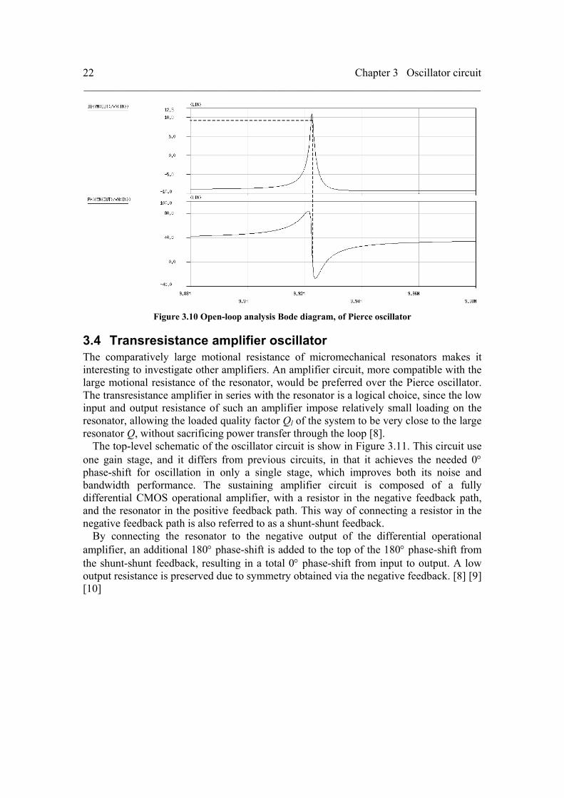
3.3.2 Open-loop analysis An open-loop analysis is performed, according to Appendix B, to determine whether the circuit will oscillate. The frequency is swept from 1 kHz to 10 MHz and the gain and the phase is plotted in the Bode diagram shown in Figure 3.10. In this figure, the interesting region closest to the resonance frequency of the resonator is shown. The Bode diagram shows that the conditions for sustained oscillation are fulfilled. At 0° phase-shift the open-loop gain is 9.5 dB.
The open-loop analysis can also be used for calculating the loaded quality factor Ql of the circuit. Formula (1.6) gives:
12465796
10922.9 6
=⋅
=lQ
This value is 56% of the resonator’s Q, which is acceptable. To further improve the Ql, the loading on the resonator should be decreased. It is hard to improve the Ql, because Ql depends on the relation between the resonator’s series resistance Rs and the load impedance on the resonator. For MEMS-resonators Rs is relatively large, which will demand even larger load impedance for a Ql close to the resonator’s Q. There is a trade-off between high gain and high Ql. When the size of capacitance C1 and C2 increases, the loaded quality factor will increase and the open-loop gain will decrease. This means that when the phase-noise of the oscillator is improved the amplifier will have longer startup time.
The working point of the oscillator is very close to steepest part of the phase curve, indicating good phase noise performance, according to [23]. It is possible to optimize the working point even further by changing the value of the capacitances, C1 and C2. From this Bode diagram, under the assumption that the model of the resonator is correct, it is possible to conclude that the circuit will oscillate.
Chapter 3 Oscillator circuit _______________________________________________________________________
22
Figure 3.10 Open-loop analysis Bode diagram, of Pierce oscillator
3.4 Transresistance amplifier oscillator The comparatively large motional resistance of micromechanical resonators makes it interesting to investigate other amplifiers. An amplifier circuit, more compatible with the large motional resistance of the resonator, would be preferred over the Pierce oscillator. The transresistance amplifier in series with the resonator is a logical choice, since the low input and output resistance of such an amplifier impose relatively small loading on the resonator, allowing the loaded quality factor Ql of the system to be very close to the large resonator Q, without sacrificing power transfer through the loop [8].
The top-level schematic of the oscillator circuit is show in Figure 3.11. This circuit use one gain stage, and it differs from previous circuits, in that it achieves the needed 0° phase-shift for oscillation in only a single stage, which improves both its noise and bandwidth performance. The sustaining amplifier circuit is composed of a fully differential CMOS operational amplifier, with a resistor in the negative feedback path, and the resonator in the positive feedback path. This way of connecting a resistor in the negative feedback path is also referred to as a shunt-shunt feedback.
By connecting the resonator to the negative output of the differential operational amplifier, an additional 180° phase-shift is added to the top of the 180° phase-shift from the shunt-shunt feedback, resulting in a total 0° phase-shift from input to output. A low output resistance is preserved due to symmetry obtained via the negative feedback. [8] [9] [10]

3.4 Transresistance amplifier oscillator _______________________________________________________________________
23
+
+ _
_
Fully Differential Amplifier
Rf
Output buffer
+
_
Figure 3.11 Top-level circuit schematic of the transresistance amplifier oscillator
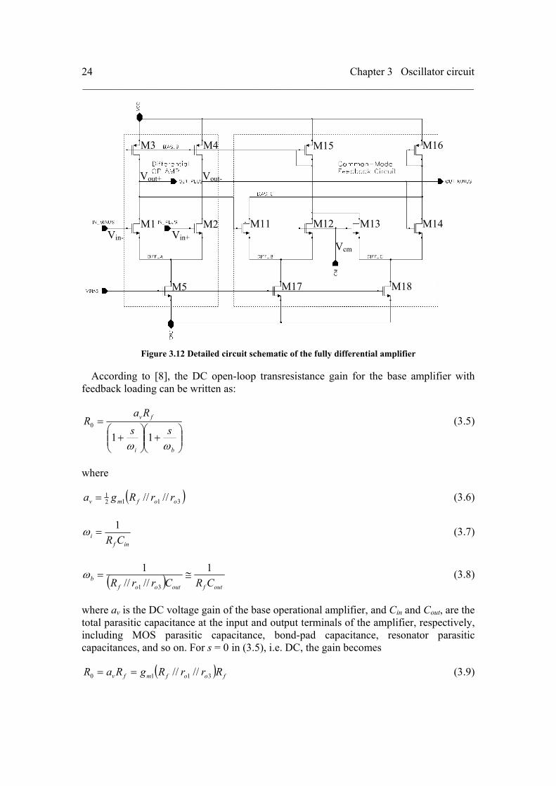
3.4.1 Detailed circuit schematic In detailed circuit schematic of Figure 3.12, the fully differential amplifier is comprised of a basic single-stage, differential operational amplifier (transistors M1 – M5), and a common-mode feedback circuit (transistors M11 – M18), that sets up the DC bias point.
The common-mode feedback circuit compares the two output voltages, Vout+ and Vout-, of the differential operational amplifier, to the common-mode voltage Vcm. The common-mode feedback circuit will then make the DC voltages at the outputs of the differential operational amplifier settle at a DC voltage equal to Vcm. For example, if the DC voltage Vout+ rises, the current through transistor M11 will increase, which will make the current through transistor M12 decrease. The current through transistor M12 is then copied in the current mirror M3 M15, back to the differential operational amplifier, i.e. the current through transistor M1 will also decrease, which will make the DC voltage Vout+ drop back and settle at the same voltage as Vcm.
This investigation has shown that this way of making the common-mode feedback circuit has one big advantage, and that is that it does not put a resistor in parallel with the resonator. The most common way of making a common-mode feedback circuit is by putting two resistors in series between Vout+ and Vout-, and then taking the average voltage between these two resistors and comparing it to the common-mode voltage Vcm. These two resistors, plus the feedback resistor Rf, would be in parallel with the resonator, which would severely degrade the startup time of the oscillator.
Chapter 3 Oscillator circuit _______________________________________________________________________
24
M5
M4 M3
M12 M13 M14
M18 M17
M11M1 M2
M15 M16
Vout+ Vout-
Vin- Vin+ Vcm
Figure 3.12 Detailed circuit schematic of the fully differential amplifier
According to [8], the DC open-loop transresistance gain for the base amplifier with feedback loading can be written as:
⎟⎟⎠
⎞⎜⎜⎝
⎛+⎟⎟
⎠
⎞⎜⎜⎝
⎛+
=
bi
fv
ssRa
R
ωω11
0 (3.5)
where
( )31121 //// oofmv rrRga = (3.6)
infi CR
1=ω (3.7)
( ) outfoutoofb CRCrrR
1////1
31
≅=ω (3.8)
where av is the DC voltage gain of the base operational amplifier, and Cin and Cout, are the total parasitic capacitance at the input and output terminals of the amplifier, respectively, including MOS parasitic capacitance, bond-pad capacitance, resonator parasitic capacitances, and so on. For s = 0 in (3.5), i.e. DC, the gain becomes
( ) foofmfv RrrRgRaR 3110 ////== (3.9)
3.4 Transresistance amplifier oscillator _______________________________________________________________________
25
From (3.5), it is also possible to derive the expression of the effective bandwidth:
( )[ ]21
21
21
, 22
1⎥⎥⎦
⎤
⎢⎢⎣
⎡ +≅+≅
outinf
fmvbieffb CCR
Rgaωωω (3.10)
From formula (C.1), (C.2) and (C.3) in Appendix C, with R0 = gm1(Rf//ro1//ro3)Rf, gmF = 1/Rf, Rin = Rf, and Rout = Rf//ro1//ro3, it follows that expressions for the closed-loop DC transresistance gain, input resistance and output resistance, of the transresistance amplifier can be written as:
( )( ) f
fm
fm
oofm
foofmamp R
RgRg
rrRgRrrRg
R ≅+
≅+
=1
21
31121
31121
2////1////
(3.11)
( ) 1131121
22
2////1 mfm
f
oofm
fi gRg
RrrRg
RR ≅
+≅
+= (3.12)
( ) 1131121
31 22
2////1
////
mfm
f
oofm
oofo gRg
RrrRg
rrRR ≅
+≅
+≅ (3.13)
For more information on how to derive these equations see [21] and [22]. These equations are also consistent with the results in [8].
In practice, the transresistance gain Ramp depends mainly on Rf, while the input resistance Ri and output resistance Ro depend mainly on the transconductance gm of the input transistors, suggesting that larger input transistors W/L ratios or larger bias currents can further reduce the input and output resistance. The use of larger input transistors can impact the 3-dB bandwidth of the transresistance amplifier, which as a rule should be at least ten times larger than the oscillation frequency so that its phase-shift at this frequency is minimal. From the expression of the effective bandwidth, decreasing Cin and Rf, and increasing the gain-bandwidth product gm1Rf of the amplifier increases the bandwidth. This places a limit on how large the W/L ratio of the input transistors can be made, since Cin grows faster than gm with increasing W, hence, bandwidth suffers. Bandwidth needs constrain Rf to a maximum allowable value, while loop gain needs set its minimum value. According to [8], the loop gain must fulfill the following relation:
oisampf RRRRR ++≥≅ (3.14)
where, Ramp is the closed-loop gain of the transresistance amplifier, Rs is the series resistance of the resonator, and Ri and Ro are the input and output resistance of the transresistance amplifier, respectively. This relation gives the lower limit on the feedback resistance. But the effective bandwidth should also be at least ten times larger than the resonance frequency, which is about 9.922 MHz. Solving (3.10) for Rf, gives the upper limit on the feedback resistance.

Chapter 3 Oscillator circuit _______________________________________________________________________
26
( )( )resoutin
resoutinmm
effboutin
effboutinmm
f CCCCgg
CC
CCggR
ωω
ω
ω
1041016
4
16 2211
,
2,
21)(1 ++
≤++
= − (3.15)
The second solution is disregarded, because the feedback resistance can only have a positive value, and therefore the minus sign is removed. To be able to calculate numeric values of the upper and lower limit of the feedback resistance Rf, the value of the transconductance gm1 of transistor M1, and the parasitic capacitance at the input and output terminals of the amplifier must be found. The transconductance is found by simulation, and its value is 125×10-6 Ω-1. This result is used in (3.12) and (3.13), which give the values of the input and output resistance, respectively. It is hard to find an exact value on the parasitic capacitances. In practice, the only thing that is possible is to make a qualified guess. If all the parasitics are taken into account, MOS parasitic capacitance, bond-pad capacitance, bond-wire capacitance, resonator parasitic capacitances and bias module, a total capacitance of 100 fF at both terminals is most likely an underestimate. According to (3.14) and (3.15) the upper and lower values for Rf are:
333366
3 104210161016101010125
210125
21010 ×=×+×+×=×
+×
+×≥ −−fR (3.16)
and
( ) ( )( )
3
261515
261515266
10261021.921010100101004
1021.92101010010100161012510125
×≈
≈×⋅⋅×⋅×⋅
×⋅⋅×⋅×⋅+×+×≤
−−
−−−−
ππ
fR (3.17)
Even for such a low value on the parasitic capacitances the maximum value is smaller than the minimum value of the feedback resistance, i.e. this circuit will most likely not oscillate in reality or if it oscillates it will have poor phase-noise performance.
Even though the transresistance amplifier is sensitive to parasitic capacitances at the input and output terminals and has poor phase-noise performance in this technology, it is designed and a layout is made, so it can be tested in simulation.
Figure 3.13 presents the circuit schematic of the final transresistance amplifier oscillator, with bias circuit and output buffer. The two blocks to the left sets the common-mode voltage for the common-mode feedback circuit, and the bias voltage for the transresistance amplifier and the output buffer. The virtual ground is set to the same voltage as the common-mode voltage. This will make the DC voltage at both inputs of the differential operational amplifier equal to Vcm, because the only DC current flowing to or from Vin- is to Vout+, which has a DC voltage equal to Vcm, because of the common-mode feedback circuit.
To make testing easier the fully differential amplifier uses another voltage source then the rest of the circuit. The reason for this is to be able to control the amplitude of the voltage driving the resonator. By lowering the Vdc for the fully differential amplifier, transistors M3, M4, M15 and M16 in Figure 3.12 will enter the linear region at a lower

3.4 Transresistance amplifier oscillator _______________________________________________________________________
27
voltage level, resulting in a smaller voltage swing at the outputs of the fully differential amplifier. This will give the possibility to drive the resonator at a lower power level.
Figure 3.13 Circuit schematic of the transresistance amplifier oscillator
3.4.2 Open-loop analysis An open-loop analysis in performed, according to Appendix B, to verify that this circuit will oscillate. This open-loop analysis is made without parasitic capacitances. The value of feedback resistance Rf, is 60 kΩ. This value is a compromise, according to bandwidth needs it should be smaller and according to loop gain needs (gain > 3 dB for fast startup time [8]) it should be larger. This results in a circuit that has poor phase noise performance and long startup time (>1 ms), but it will oscillate.
The gain at 0° phase-shift is 6.4 dB, so ideally this circuit will oscillate. But it is known from theory that this circuit is sensitive to parasitic capacitances. The working point of the oscillator is not in the steepest part of the phase curve, indicating poor phase noise performance. Small variations in phase will lead to relatively big variations in oscillation frequency. It is not possible to compensate for this phase-shift as in the Pierce oscillator.
That this circuit will have poor phase-noise performance can also be seen if the load quality factor Ql of this circuit is calculated, (1.6) gives:
39512511
10922.9 6
=⋅
=lQ (3.18)
This means that Ql for the circuit is only about 18% of the resonator’s Q, which is not good for the phase-noise.

Chapter 3 Oscillator circuit _______________________________________________________________________
28
Ideal working point
Figure 3.14 Open-loop analysis Bode diagram, of transresistance amplifier oscillator
By adding two shunt capacitances at the input and output of the fully differential amplifier, respectively, and change the value of these capacitances in four steps between 100 fF and 400 fF, the affects of parasitic capacitance will show up in the Bode diagram. The result is plotted in the Bode diagram in Figure 3.15. It is possible to see, that for parasitic capacitance somewhere between 300 fF and 400 fF the phase curve does not cross zero, and therefore, the circuit will not oscillate for parasitic capacitance above this value. The more phase-shift there is, the further away from the ideal working point in the steepest part of the phase curve, it gets. Therefore, more parasitics will lead to more phase noise.

3.4 Transresistance amplifier oscillator _______________________________________________________________________
29
100 fF 200 fF 300 fF 400 fF
Figure 3.15 Open-loop analysis Bode diagram, of transresistance amplifier oscillator. The phase curves, from top to bottom, are for parasitic capacitances of 100 fF, 200 fF, 300 fF and 400 fF,
respectively.

31
Chapter 4 Layout
The Pierce oscillator and the transresistance amplifier oscillator are implemented in the A-BCD2 process. These layouts are tested and simulated. A final layout of the Pierce oscillator, with bond-pads and ESD protection, is made. This final chip layout is manufactured at Philips Semiconductors in Nijmegen, The Netherlands.
4.1 A-BCD2 process The oscillator will be implemented in a process called A-BCD2, which is the abbreviation for Advanced-Bipolar-CMOS-DMOS 2. A-BCD is a family of 100 V BCD processes on Silicon-On-Insulator. These processes are offering latchup free operation, robustness, good EMC performance, high package density and low mask count. It comes from Philips Semiconductors in Nijmegen, The Netherlands. A-BCD2 is capable of handling 120 V on chip and it has several vital features that are important when designing a MEMS based oscillator:
• It is convenient to integrate MEMS devices in SOI processes. • A MEMS-resonator needs a DC voltage of between 5 and 100 V to resonate and
this process can handle such high voltages on chip. • If a future product is going to use a supply voltage of about 3 V it needs to be
transformed to higher voltages with a DCDC-converter. Philips already has some DCDC-converters designed in this process and they can easily be integrated on the same chip as the oscillator.
• The A-BDC2 process is a cheep and simple process and this is important when entering a market with highly competitive prices.
There are some disadvantages with this process also. The primary problem with this process is that it seems to suffer from quite large parasitics. This is a problem in some

Chapter 4 Layout _______________________________________________________________________
32
oscillator designs, especially the transresistance amplifier oscillator. For more information about the A-BCD2 process see [25].
4.1.1 SOI technology Silicon-on-Insulator differs from CMOS by placing the transistor’s silicon junction area on top of an electrical insulator. The most common insulators employed with this technique are glass and silicon oxide. For the A-BCD2 process, the insulator is silicon oxide. With the SOI technique, the gate area can be assured of minimal capacitance. A low capacitance circuit will allow faster transistor operation and as transistor latency drops, the ability to process more instructions in a given time rises. This is the reason why this technology has become so popular in resent years. For more information about SOI technology see [18].
4.2 Pierce oscillator layout Figure 4.1 shows the layout of the Pierce oscillator. To the left are the five P-well resistors, in the middle the inverting amplifier with bias circuit, and to the right the output buffer.
Figure 4.1 Pierce oscillator, size about 190×120 µm
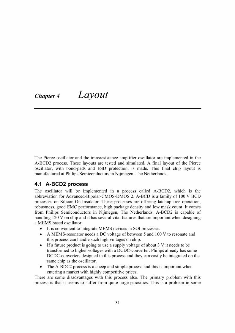
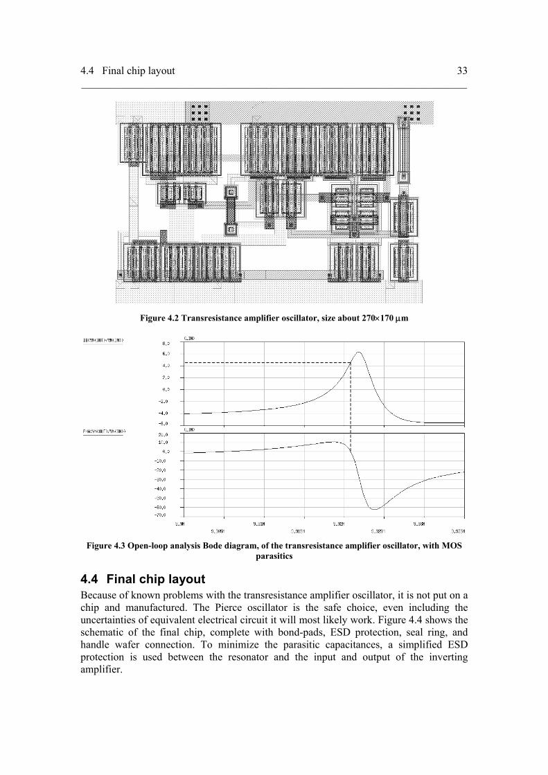
4.3 Transresistance amplifier oscillator layout In Figure 4.2 the layout of the transresistance amplifier oscillator is shown, complete with bias circuit and output buffer. A parasitic extraction is made of this layout, and it is simulated. As shown in Figure 4.3, just the MOS parasitics give almost enough phase-shift to make it stop working. It is also far from the ideal working point in the steepest part of the phase curve, indicating that it will have poor phase noise performance.
4.4 Final chip layout _______________________________________________________________________
33
Figure 4.2 Transresistance amplifier oscillator, size about 270×170 µm
Figure 4.3 Open-loop analysis Bode diagram, of the transresistance amplifier oscillator, with MOS
parasitics
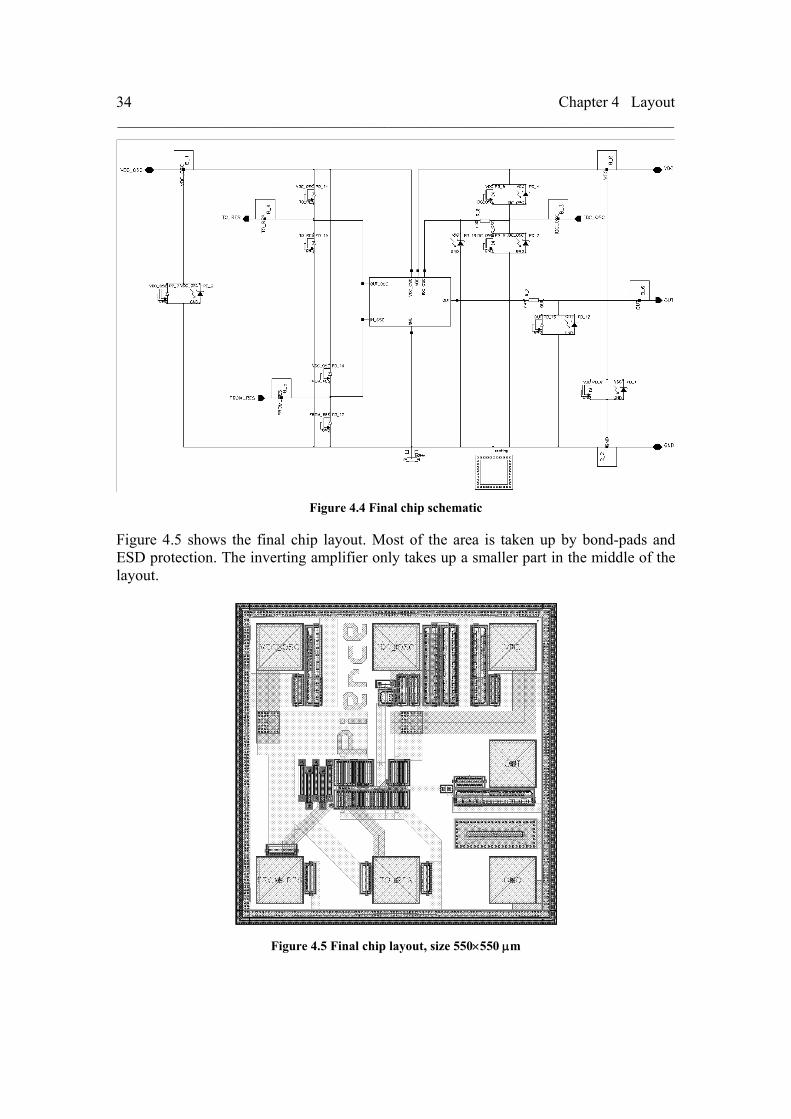
4.4 Final chip layout Because of known problems with the transresistance amplifier oscillator, it is not put on a chip and manufactured. The Pierce oscillator is the safe choice, even including the uncertainties of equivalent electrical circuit it will most likely work. Figure 4.4 shows the schematic of the final chip, complete with bond-pads, ESD protection, seal ring, and handle wafer connection. To minimize the parasitic capacitances, a simplified ESD protection is used between the resonator and the input and output of the inverting amplifier.
Chapter 4 Layout _______________________________________________________________________
34
Figure 4.4 Final chip schematic
Figure 4.5 shows the final chip layout. Most of the area is taken up by bond-pads and ESD protection. The inverting amplifier only takes up a smaller part in the middle of the layout.
Figure 4.5 Final chip layout, size 550×550 µm
4.4 Final chip layout _______________________________________________________________________
35
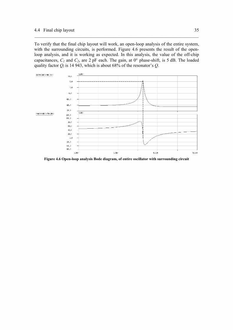
To verify that the final chip layout will work, an open-loop analysis of the entire system, with the surrounding circuits, is performed. Figure 4.6 presents the result of the open-loop analysis, and it is working as expected. In this analysis, the value of the off-chip capacitances, C1 and C2, are 2 pF each. The gain, at 0° phase-shift, is 5 dB. The loaded quality factor Ql is 14 943, which is about 68% of the resonator’s Q.
Figure 4.6 Open-loop analysis Bode diagram, of entire oscillator with surrounding circuit


37
Chapter 5 Final measurements
This chapter presents the final measurement of the Pierce oscillator chip manufactured at Philips Semiconductors in Nijmegen. A test board, for the Pierce oscillator and the resonator, is constructed. The entire test board is put into a vacuum chamber and measured. Table 5.1 shows the information about the Pierce oscillator samples, which the measurements are made on. Batch N5A1E9A Wafer no. 1 Process code L1082EA (A-BCD2-HV including SND and CH mask) Maskset ECI796 Circuit name Pierce
Table 5.1 Pierce oscillator samples information
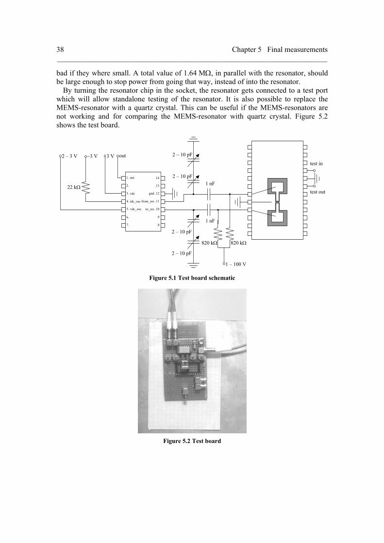
5.1 Test board In order to measure the chip with the Pierce oscillator, a test board is constructed according to the schematic in Figure 5.1. This test board includes the off-chip capacitances, C1 and C2, and the bias circuit for the oscillator and the resonator. From the simulations in previous chapters, the expected value on capacitance, C1 and C2, is between 0.8 and 2 pF each. The variable capacitors can only deliver a capacitance of between 2 and 10 pF, and therefore two of them are put in series on each side of the resonator, which will give a total capacitance of between 1 and 5 pF.
With a 3 V input, the 22 kΩ resistor will deliver a bias current of about 100 µA to the oscillator. The two 820 kΩ resistances are in parallel with the resonator, which would be
Chapter 5 Final measurements _______________________________________________________________________
38
bad if they where small. A total value of 1.64 MΩ, in parallel with the resonator, should be large enough to stop power from going that way, instead of into the resonator.
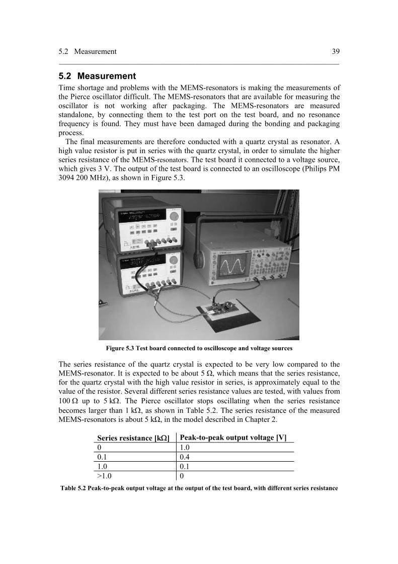
By turning the resonator chip in the socket, the resonator gets connected to a test port which will allow standalone testing of the resonator. It is also possible to replace the MEMS-resonator with a quartz crystal. This can be useful if the MEMS-resonators are not working and for comparing the MEMS-resonator with quartz crystal. Figure 5.2 shows the test board.
3. vdc
4. idc_osc
5. vdc_osc
gnd .12
from_res .11
to_res .10
1. out
2.
6.
7.
.14
.13
.9
.8
22 kΩ
2 – 3 V ~3 V out
1 – 100 V
3 V
1 nF
820 kΩ
2 – 10 pF
2 – 10 pF
1 nF
820 kΩ
2 – 10 pF
2 – 10 pF
test in
test out
Figure 5.1 Test board schematic
Figure 5.2 Test board
5.2 Measurement _______________________________________________________________________
39
5.2 Measurement Time shortage and problems with the MEMS-resonators is making the measurements of the Pierce oscillator difficult. The MEMS-resonators that are available for measuring the oscillator is not working after packaging. The MEMS-resonators are measured standalone, by connecting them to the test port on the test board, and no resonance frequency is found. They must have been damaged during the bonding and packaging process.
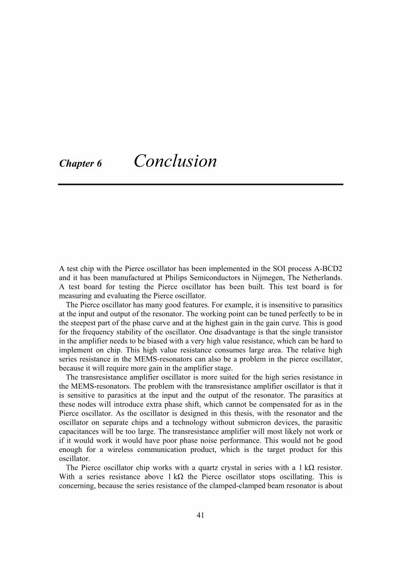
The final measurements are therefore conducted with a quartz crystal as resonator. A high value resistor is put in series with the quartz crystal, in order to simulate the higher series resistance of the MEMS-resonators. The test board it connected to a voltage source, which gives 3 V. The output of the test board is connected to an oscilloscope (Philips PM 3094 200 MHz), as shown in Figure 5.3.
Figure 5.3 Test board connected to oscilloscope and voltage sources
The series resistance of the quartz crystal is expected to be very low compared to the MEMS-resonator. It is expected to be about 5 Ω, which means that the series resistance, for the quartz crystal with the high value resistor in series, is approximately equal to the value of the resistor. Several different series resistance values are tested, with values from 100 Ω up to 5 kΩ. The Pierce oscillator stops oscillating when the series resistance becomes larger than 1 kΩ, as shown in Table 5.2. The series resistance of the measured MEMS-resonators is about 5 kΩ, in the model described in Chapter 2.
Series resistance [kΩ] Peak-to-peak output voltage [V] 0 1.0 0.1 0.4 1.0 0.1 >1.0 0
Table 5.2 Peak-to-peak output voltage at the output of the test board, with different series resistance

41
Chapter 6 Conclusion
A test chip with the Pierce oscillator has been implemented in the SOI process A-BCD2 and it has been manufactured at Philips Semiconductors in Nijmegen, The Netherlands. A test board for testing the Pierce oscillator has been built. This test board is for measuring and evaluating the Pierce oscillator.
The Pierce oscillator has many good features. For example, it is insensitive to parasitics at the input and output of the resonator. The working point can be tuned perfectly to be in the steepest part of the phase curve and at the highest gain in the gain curve. This is good for the frequency stability of the oscillator. One disadvantage is that the single transistor in the amplifier needs to be biased with a very high value resistance, which can be hard to implement on chip. This high value resistance consumes large area. The relative high series resistance in the MEMS-resonators can also be a problem in the pierce oscillator, because it will require more gain in the amplifier stage.
The transresistance amplifier oscillator is more suited for the high series resistance in the MEMS-resonators. The problem with the transresistance amplifier oscillator is that it is sensitive to parasitics at the input and the output of the resonator. The parasitics at these nodes will introduce extra phase shift, which cannot be compensated for as in the Pierce oscillator. As the oscillator is designed in this thesis, with the resonator and the oscillator on separate chips and a technology without submicron devices, the parasitic capacitances will be too large. The transresistance amplifier will most likely not work or if it would work it would have poor phase noise performance. This would not be good enough for a wireless communication product, which is the target product for this oscillator.
The Pierce oscillator chip works with a quartz crystal in series with a 1 kΩ resistor. With a series resistance above 1 kΩ the Pierce oscillator stops oscillating. This is concerning, because the series resistance of the clamped-clamped beam resonator is about
Chapter 6 Conclusion _______________________________________________________________________
42
5 kΩ. The gain of the Pierce oscillator might be too small, but it is difficult to draw a final conclusion saying that the Pierce oscillator does not have enough gain, because it is working in the simulations made in Cadence, which uses the model of clamped-clamped beam resonator that fits measured data. It needs to be tested with the clamped-clamped beam resonator, in order to draw a final conclusion, saying whether the Pierce oscillator will work or not with the clamped-clamped beam resonator.
6.1 Future work There are a lot of improvements that can be made to the oscillator design presented in this work. Some of them are related to performance and others are related to controllability, which is important in a future MEMS based oscillator product.
6.1.1 Automatic level control Automatic level control could further improve the frequency stability of the oscillator. As shown in [16], oscillator limiting via resonator nonlinearity seems to introduce a 1/f3 phase noise component that dominates the close-to-carrier phase noise of micromechanical resonators. Automatic level control is monitoring the output signal from the amplifier in the oscillator and limits its amplitude by comparing it to a reference voltage. This way of limiting via electronic methods, rather than by mechanical resonator nonlinearity, will reduce the close-to-carrier phase noise.
6.1.2 Compensating for temperature variations In order for the MEMS based oscillator to be a successful replacement for the quartz crystal oscillator, the relatively large frequency shift when temperature changes needs to be removed. As shown in Appendix D, the frequency shift is about 8 ppm/°C for the clamped-clamped beam resonators. For a reference oscillator this is not good enough. The requirement for a reference oscillator is a total frequency shift of less than 2 ppm from 0°C to 70°C. The DC voltage will also shift the resonance frequency about 200 ppm/V. Hence, the DC voltage can be used to control the resonance frequency and compensate for any frequency shift when temperature changes. Measuring the temperature on-chip and changing the DC voltage in a corresponding manner can remove the frequency shift. This would be one method of compensating for temperature variations.
6.1.3 Integrating resonator and circuit on same chip The A-BCD process family offers the possibility of integrating the resonator on the same chip as the circuit part of the oscillator. At Philips Semiconductors, the work on integrating the resonator in the A-BCD process is already far ahead. With the resonator and the amplifier on the same chip, the parasitic capacitances would be reduced, which would give the possibility of further phase noise improvements.
6.1.4 Frequency calibration Because of process spread the exact resonance frequency of the resonator is impossible to know before manufacturing. In a future product, it must be possible to tune the oscillation frequency. This can be done with a memory, which would be set after manufacturing.

6.1 Future work _______________________________________________________________________
43
This memory would control the DC voltage on the resonator. By changing the DC voltage to a proper level, the resonance frequency of the resonator could be tuned perfectly at the target frequency.


45
Appendix A ADS optimization setup
In this appendix the ADS optimization setups, for the characterization of the MEMS-resonators, are presented. All the setups that are presented here will fit an equivalent electrical circuit of the MEMS-resonator, to measured S-parameter data.

Appendix A ADS optimization setup _______________________________________________________________________
46
A.1 Measurement setup 1 This setup is for fitting the equivalent electrical circuit presented in Figure 2.3 to measured S-parameter data. The second goal forces the optimizer to be much more accurate at the resonance frequency, because it is the most important frequency point. Without this extra goal the fit will not be good at the resonance frequency.
Figure A.1 Measurement setup 1

A.2 Measurement setup 2 _______________________________________________________________________
47
A.2 Measurement setup 2 This setup is for fitting the equivalent electrical circuit presented in Figure 2.5 to measured S-parameter data. The second goal forces the optimizer to be much more accurate in the region closest to the resonance frequency (9.92175 MHz – 9.92225 MHz). This method will give the best result for this circuit.
Figure A.2 Measurement setup 2
Appendix A ADS optimization setup _______________________________________________________________________
48
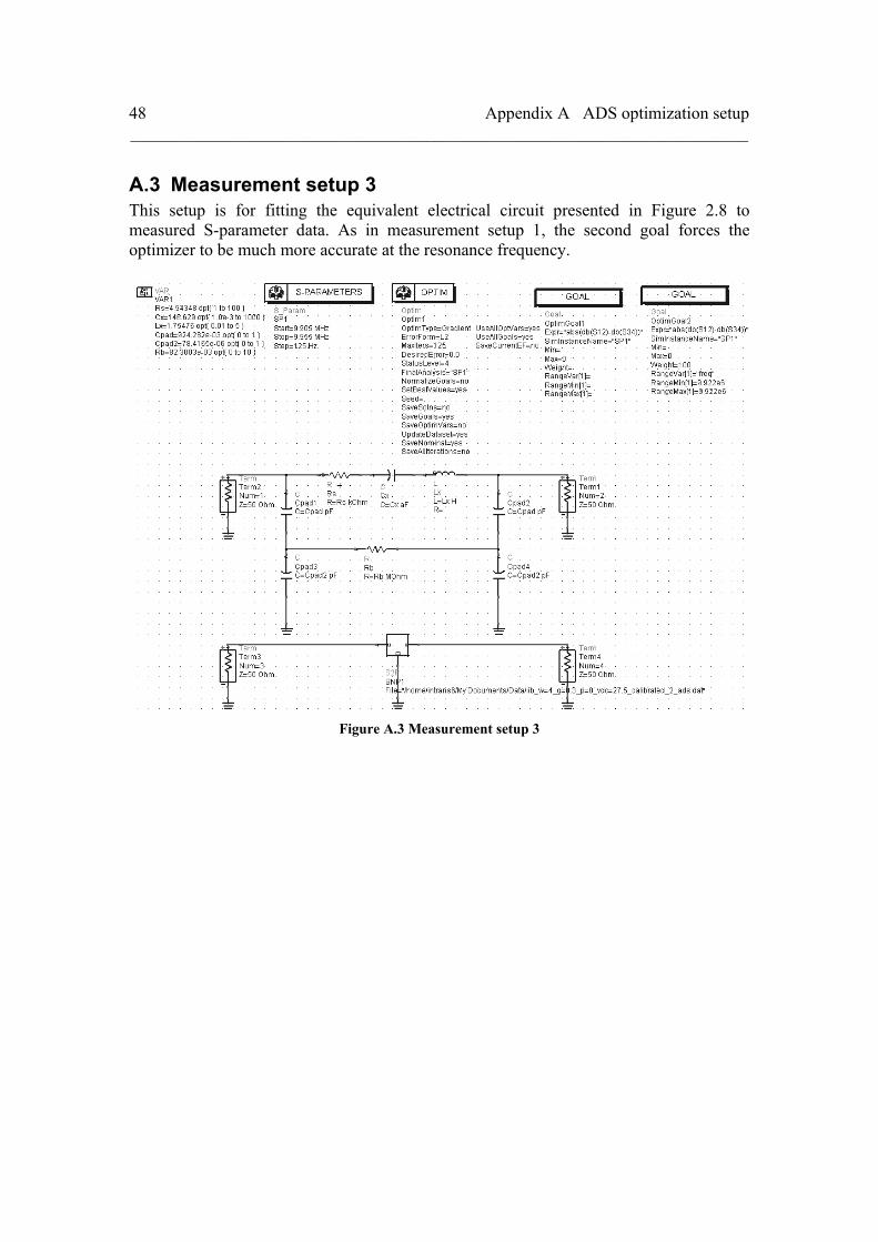
A.3 Measurement setup 3 This setup is for fitting the equivalent electrical circuit presented in Figure 2.8 to measured S-parameter data. As in measurement setup 1, the second goal forces the optimizer to be much more accurate at the resonance frequency.
Figure A.3 Measurement setup 3

49
Appendix B Open-loop analysis
In this appendix the open-loop tool is explained and the open-loop simulation setup for the pierce oscillator and the transresistance amplifier oscillator are presented. To determine whether a circuit will oscillate an open-loop analysis must be performed. To be able to perform the open-loop analysis a special circuit is needed which is called open-loop analysis tool. This tool makes it possible to perform an open-loop analysis with the circuit operating under nominal DC biasing conditions. Furthermore, the tool makes the AC operating conditions (namely loading and reverse action effects) during open-loop analysis consistent with the normal operation mode of the circuit.
The open-loop analysis tool connects the circuit under investigation to a dummy circuit, which is identical to the circuit being analyzed. The gain and phase-shift around the loop, of the oscillator circuit, is plotted in a Bode diagram. If the gain at 0° phase-shift is greater the 0 dB, the circuit will oscillate.
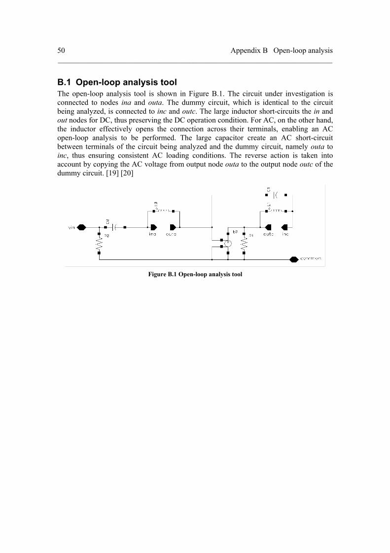
Appendix B Open-loop analysis _______________________________________________________________________
50
B.1 Open-loop analysis tool The open-loop analysis tool is shown in Figure B.1. The circuit under investigation is connected to nodes ina and outa. The dummy circuit, which is identical to the circuit being analyzed, is connected to inc and outc. The large inductor short-circuits the in and out nodes for DC, thus preserving the DC operation condition. For AC, on the other hand, the inductor effectively opens the connection across their terminals, enabling an AC open-loop analysis to be performed. The large capacitor create an AC short-circuit between terminals of the circuit being analyzed and the dummy circuit, namely outa to inc, thus ensuring consistent AC loading conditions. The reverse action is taken into account by copying the AC voltage from output node outa to the output node outc of the dummy circuit. [19] [20]
Figure B.1 Open-loop analysis tool

B.2 Simulation setup for the Pierce oscillator _______________________________________________________________________
51
B.2 Simulation setup for the Pierce oscillator The Pierce oscillator circuit is opened between the resonator and the gate of the amplifier transistor, as shown in the simulation setup in Figure B.2. Capacitances, C1 and C2, are added, each with a capacitance of 2 pF. The bias current is set to 100 µA. The open-loop analysis tool connects the circuit under investigation to the dummy circuit, which is identical to the circuit being analyzed.
Figure B.2 Open-loop analysis, Pierce oscillator
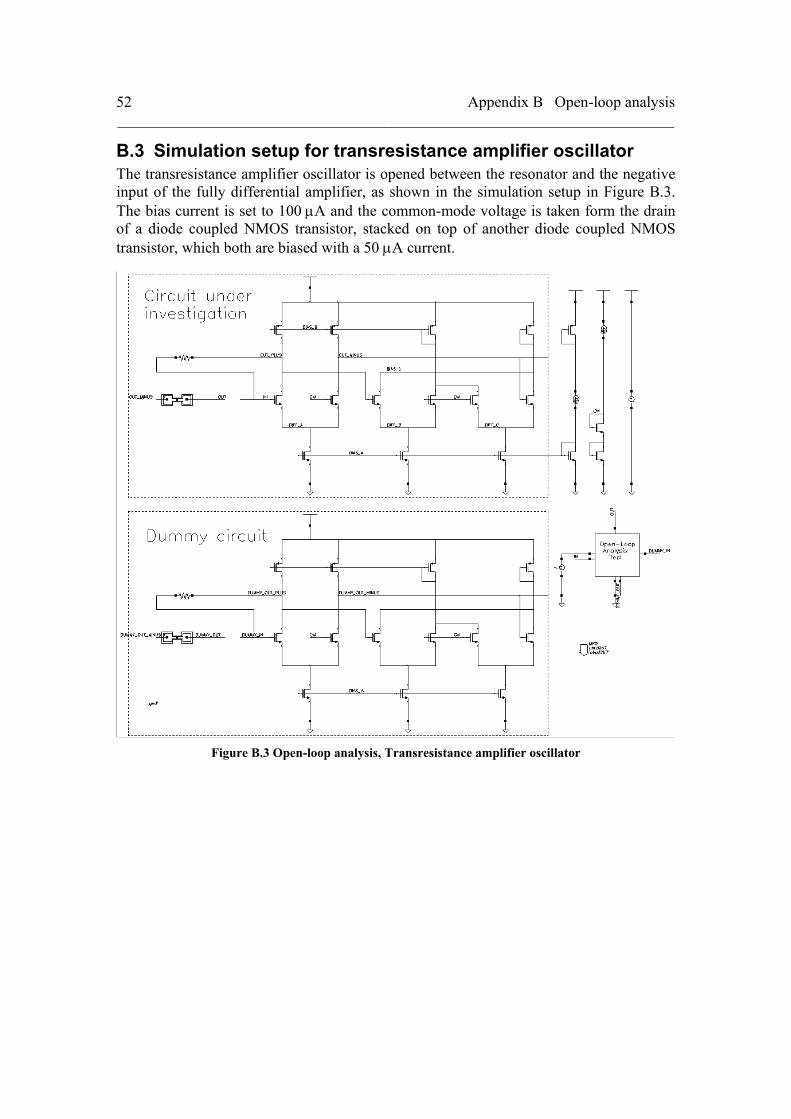
Appendix B Open-loop analysis _______________________________________________________________________
52
B.3 Simulation setup for transresistance amplifier oscillator The transresistance amplifier oscillator is opened between the resonator and the negative input of the fully differential amplifier, as shown in the simulation setup in Figure B.3. The bias current is set to 100 µA and the common-mode voltage is taken form the drain of a diode coupled NMOS transistor, stacked on top of another diode coupled NMOS transistor, which both are biased with a 50 µA current.
Figure B.3 Open-loop analysis, Transresistance amplifier oscillator
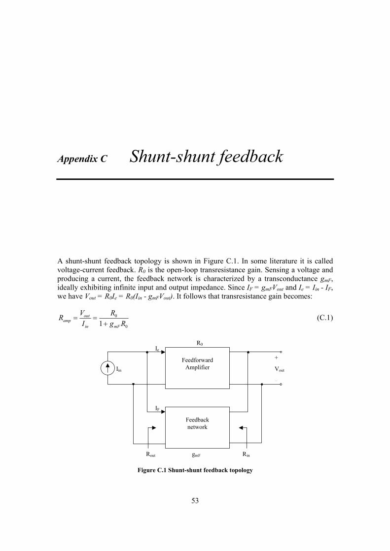
53
Appendix C Shunt-shunt feedback
A shunt-shunt feedback topology is shown in Figure C.1. In some literature it is called voltage-current feedback. R0 is the open-loop transresistance gain. Sensing a voltage and producing a current, the feedback network is characterized by a transconductance gmF, ideally exhibiting infinite input and output impedance. Since IF = gmFVout and Ie = Iin - IF, we have Vout = R0Ie = R0(Iin - gmFVout). It follows that transresistance gain becomes:
0
0
1 RgR
IVR
mFin
outamp +
== (C.1)
Feedforward
Amplifier
Feedback network
Iin
Ie
Rout Rin
IF
gmF
Vout
R0
+
_
Figure C.1 Shunt-shunt feedback topology
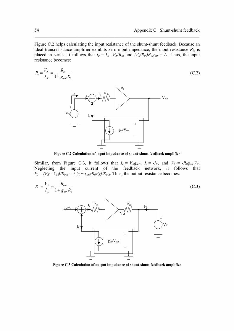
Appendix C Shunt-shunt feedback _______________________________________________________________________
54
Figure C.2 helps calculating the input resistance of the shunt-shunt feedback. Because an ideal transresistance amplifier exhibits zero input impedance, the input resistance Rin is placed in series. It follows that IF = IX - VX/Rin and (Vx/Rin)R0gmF = IF. Thus, the input resistance becomes:
01 RgR
IVR
mF
in
X
Xi +
== (C.2)
gmFVout
IF
Ie Rin IX
VX
R0
Vout + _
+
+
_
Figure C.2 Calculation of input impedance of shunt-shunt feedback amplifier
Similar, from Figure C.3, it follows that IF = VXgmF, Ie = -IF, and VM = -R0gmFVX. Neglecting the input current of the feedback network, it follows that IX = (VX - VM)/Rout = (VX + gmFR0VX)/Rout. Thus, the output resistance becomes:
01 RgR
IVR
mF
out
X
Xo +
== (C.3)
gmFVout
IF
Ie Rin Iin=0 +
_
+
_
VX
+
IX Rout
VM
Figure C.3 Calculation of output impedance of shunt-shunt feedback amplifier

55
Appendix D MEMS-resonators
In this appendix the characteristics of the MEMS-resonators are discussed. Frequency variations depending on temperature, the DC voltage put on the resonator, and input power driving the resonator, is discussed. A method to compensate for temperature variations is presented.
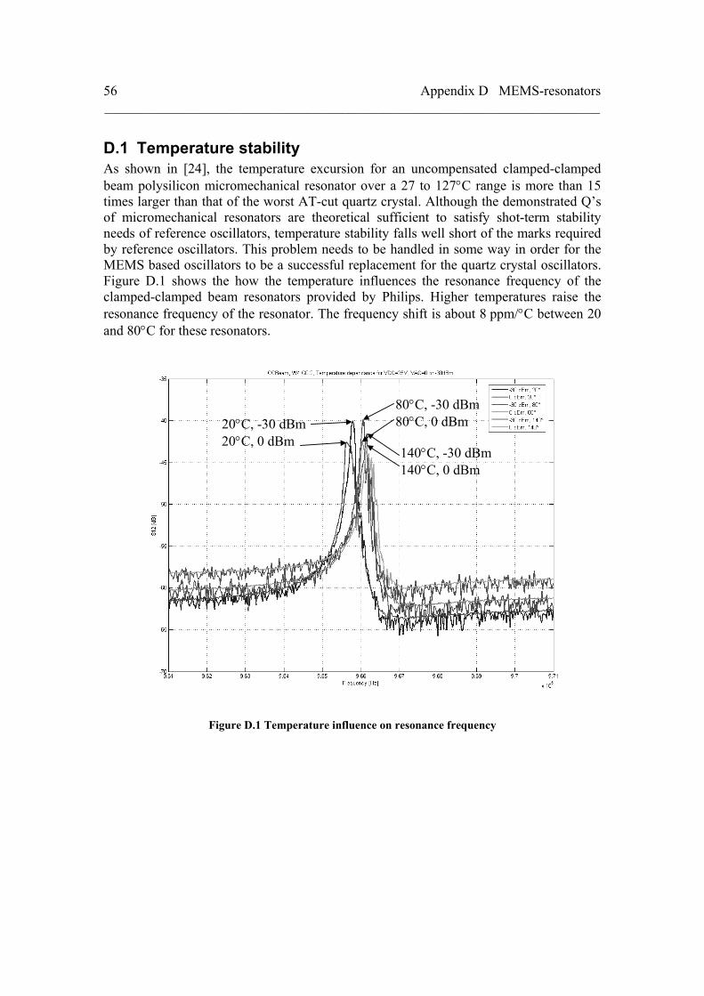
Appendix D MEMS-resonators _______________________________________________________________________
56
D.1 Temperature stability As shown in [24], the temperature excursion for an uncompensated clamped-clamped beam polysilicon micromechanical resonator over a 27 to 127°C range is more than 15 times larger than that of the worst AT-cut quartz crystal. Although the demonstrated Q’s of micromechanical resonators are theoretical sufficient to satisfy shot-term stability needs of reference oscillators, temperature stability falls well short of the marks required by reference oscillators. This problem needs to be handled in some way in order for the MEMS based oscillators to be a successful replacement for the quartz crystal oscillators. Figure D.1 shows the how the temperature influences the resonance frequency of the clamped-clamped beam resonators provided by Philips. Higher temperatures raise the resonance frequency of the resonator. The frequency shift is about 8 ppm/°C between 20 and 80°C for these resonators.
20°C, -30 dBm 20°C, 0 dBm
80°C, -30 dBm 80°C, 0 dBm
140°C, -30 dBm 140°C, 0 dBm
Figure D.1 Temperature influence on resonance frequency

D.2 DC voltage influence on resonance frequency _______________________________________________________________________
57
D.2 DC voltage influence on resonance frequency Figure D.2 shows how the DC voltage put on the resonator influences the resonance frequency. Higher DC voltages give lower resonance frequency. For these resonators, the frequency shift is about 200 ppm/V. Changing the DC voltage on the resonator could compensate for frequency shift originating from temperature variations.
10 V
25 V 22.5 V 20 V
17.5 V
15 V
12.5 V
Figure D.2 DC voltage influence on resonance frequency

Appendix D MEMS-resonators _______________________________________________________________________
58
D.3 Input power influence on resonance frequency Figure D.3 shows the influence of the input power on the resonance frequency. As seen in the figure, the resonance frequency is stable. The input power does not affect it.
Figure D.3 Input power influence on resonance frequency
D.4 Compensating for temperature variations The DC voltage on the resonator can be used to compensate for frequency shift when temperature changes. Measuring the temperature on chip and changing the DC voltage in correspondence to the temperature changes could eliminate the frequency shift. A voltage source, with an accuracy of about 40 mV/°C, and a method for measuring the temperature on chip, would be needed in order for this to work. The total voltage span would be about ±2.5 V around the center DC voltage, to compensate for the frequency shift between 20°C and 140°C.

59
References
[1] Robert J. Matthys. Crystal Oscillator Circuits, Revised Edition. Krieger Publishing Company, Malabar, Florida, 1992. ISBN 0-89464-552-8.
[2] Marvin E. Frerking. Crystal Oscillator Design and Temperature Compensation. Van Nostrand Reinhold Company, New York, 1978. ISBN 0-442-22459-1.
[3] J.T.M van Beek, Thibaut Guilloteau. Technical Note PR-TN-2004/00659, Sub-micron gap MEMS resonators for RF applications. September 2004.
[4] Paul J. Petersan, Steven M. Anlage. Measurement of resonant frequency and quality factor of microwave resonators: Comparison of methods. Center for Superconductivity Research, Department of Physics, University of Maryland, June 1998.
[5] Nhat M. Nguyen, Robert G. Meyer. Start-up and Frequency Stability in High-Frequency Oscillators. IEEE Journal of Solid-State Circuits, May 1992.
[6] Eric A. Vittoz, Marc G. R. Degrauwe, Serge Bitz. High-Performance Crystal Oscillator Circuits: Theory and Application. IEEE Journal of Solid-State Circuits, June 1988.
[7] Ville Kaajakari, Tomi Mattila, Aarne Oja, Heikki Seppä. Nonlinear Limits for Single-Crystal Silicon Microresonators. IEEE Journal of Microelectromechanical systems, October 2004.
References _______________________________________________________________________
60
[8] Yu-Wei Lin, Seungbae Lee, Sheng-Shian Li, Yuan Xie, Zeying Ren, Clark T.-C. Nguyen. Series-Resonant VHF Micromechanical Resonator Reference Oscillators. IEEE Journal of Solid-State Circuits, December 2004.
[9] Yu-Wei Lin, Seungbae Lee, Zeying Ren, Clark T.-C. Nguyen. Series-Resonant Micromechanical Resonator Oscillator. Center for Wireless Integrated Microsystems, Department of Electrical Engineering and Computer Science, University of Michigan. IEEE 2003.
[10] Yu-Wei Lin, Seungbae Lee, Sheng-Shian Li, Yuan Xie, Zeying Ren, Clark T.-C. Nguyen. 60-MHz Wine Glass Micromechanical-Disk Reference Oscillator. IEEE International Solid-State Circuits Conference. IEEE 2004.
[11] Jan Bienstman, Harrie A. C. Tilmans, Michiel Steyaert, Robert Puers. An Oscillator Circuit For Electrostatically Driven Silicon-Based One-Port Resonators. Katholieke Universiteit Leuven, Department Elektrotechniek. June 1995.
[12] Eric Vittoz, Jean Fellrath. CMOS Analog Integrated Circuits Based on Weak Inversion Operation. IEEE Journal of Solid-State Circuits. June 1977.
[13] David Salt. Handbook of Quartz Crystal Devices. Van Nostrand Reinhold (UK) Co. Ltd. 1987. ISBN 0-442-31773-5.
[14] Clark T.-C. Nguyen, Roger T. Howe. CMOS Micromechanical Resonator Oscillator. Berkeley Sensor & Actuator Center, Department of Electrical Engineering and Computer Sciences and the Electronics Research Laboratory, University of California at Berkeley. IEEE 1993.
[15] Clark T.-C. Nguyen, Roger T. Howe. An Integrated CMOS Micromechanical Resonator High-Q Oscillator. IEEE Journal of Solid-State Circuits. April 1999.
[16] Seungbae Lee, Clark T.-C. Nguyen. Influence of Automatic Level Control on Micromechanical Resonator Oscillator Phase Noise. Center for Wireless Integrated Microsystems, Department of Electrical Engineering and Computer Science, University of Michigan. IEEE 2003.
[17] Yu-Wei Lin, Seungbae Lee, Zeying Ren, Clark T.-C. Nguyen. Series-Resonant Micromechanical Resonator Oscillator. Center for Wireless Integrated Microsystems, Department of Electrical Engineering and Computer Science, University of Michigan. IEEE 2003.
[18] Jean-Pierre Colinge. Silicon-on-Insulator Technology: Materials to VLSI. Kluwer Academic Publishers, Boston, Dordrecht, London, 1991. ISBN 0-7923-9150-0.
[19] Cicero S. Vaucher. A Low Power Wide Band Non Oscillating Prescaler. Nat. Lab. Technical Note 130/92

References _______________________________________________________________________
61
[20] Melina Apostolidou, Cicero S. Vaucher. A Low-Power 20 GHz Static Frequency Divider with Programmable Input Sensitivity. Nat. Lab. Technical Note 2003/00415. Date of issue 06/2003.
[21] Paul R. Gray, Paul J. Hurst, Stephen H. Lewis, Robert G. Meyer. Analysis and Design of Analog Integrated Circuits, Fourth Edition. John Wiley & Sons, Inc., 2001. ISBN 0-471-32168-0.
[22] Behzad Razavi. Design of Analog CMOS Integrated Circuits. Tata McGraw-Hill Publishing Company Limited, New Delhi. 2002. ISBN 0-07-052903-5.
[23] Clark T.-C. Nguyen, Linda P. B. Kateni, Gabriel M. Rebeiz. Micromachined Devices for Wireless Communications. Proceedings of the IEEE. August 1998.
[24] Wan-Thai Hsu, Clark T.-C. Nguyen. Stiffness-Compensated Temperature-Insensitive Micromechanical Resonators. Center for Wireless Integrated Microsystems, Department of Electrical Engineering and Computer Science, University of Michigan. IEEE 2002.
[25] Jacob A. van der Pol, A.W Ludikhuize, H.G.A. Huizing, B. van Velzen, R.J.E. Hueting, J.F. Mom, G. van Lijnschoten, G.J.J. Hessels, E.F. Hooghoudt, R. van Huizen, M.J. Swanenberg, J.H.H.A. Egbers, F. van den Elshout, J.J. Koning, H. Schligtenhorst, J. Soeteman. A-BCD: An Economic 100V RESURF Silicon-On-Insulator BCD Technology for Consumer and Automotive Applications. IEEE 2000.
[26] Ville Kaajakari, Tomi Mattila, Aarne Oja, Jyrki Kiihamäki, Heikki Seppä. Square-Extensional Mode Single-Crystal Silicon Micromechanical Resonator for Low-Phase-Noise Oscillator Applications. IEEE 2004.
[27] T. Mattila, A. Oja, H. Seppä, O. Jaakkola. VTT Information Technology, Microsensing, Espoo, Finland. J. Kiihamäki, H Kattelus. VTT Information Technology, Microelectronics, Espoo, Finland. M. Koskenvuori, P. Rantakari, I. Tittonen. Helsinki University of Technology, Metrology Research Institute, Espoo, Finland. Micromechanical Bulk Acoustic Wave Resonators. IEEE Ultrasonics Symposium. 2002.
[28] Chris Bowick. RF Circuit Design. Newnes. 1982. ISBN 0-7506-9946-9.

På svenska Detta dokument hålls tillgängligt på Internet – eller dess framtida ersättare – under en längre tid från publiceringsdatum under förutsättning att inga extra-ordinära omständigheter uppstår.
Tillgång till dokumentet innebär tillstånd för var och en att läsa, ladda ner, skriva ut enstaka kopior för enskilt bruk och att använda det oförändrat för ickekommersiell forskning och för undervisning. Överföring av upphovsrätten vid en senare tidpunkt kan inte upphäva detta tillstånd. All annan användning av dokumentet kräver upphovsmannens medgivande. För att garantera äktheten, säkerheten och tillgängligheten finns det lösningar av teknisk och administrativ art.
Upphovsmannens ideella rätt innefattar rätt att bli nämnd som upphovsman i den omfattning som god sed kräver vid användning av dokumentet på ovan beskrivna sätt samt skydd mot att dokumentet ändras eller presenteras i sådan form eller i sådant sammanhang som är kränkande för upphovsmannens litterära eller konstnärliga anseende eller egenart.
För ytterligare information om Linköping University Electronic Press se förlagets hemsida http://www.ep.liu.se/ In English The publishers will keep this document online on the Internet - or its possible replacement - for a considerable time from the date of publication barring exceptional circumstances.
The online availability of the document implies a permanent permission for anyone to read, to download, to print out single copies for your own use and to use it unchanged for any non-commercial research and educational purpose. Subsequent transfers of copyright cannot revoke this permission. All other uses of the document are conditional on the consent of the copyright owner. The publisher has taken technical and administrative measures to assure authenticity, security and accessibility.
According to intellectual property law the author has the right to be mentioned when his/her work is accessed as described above and to be protected against infringement.
For additional information about the Linköping University Electronic Press and its procedures for publication and for assurance of document integrity, please refer to its WWW home page: http://www.ep.liu.se/ © Joel Hedestig