memory trends and implications for lithography...
TRANSCRIPT

©2015 Micron Technology, Inc.1
Linda K. Somerville, Ardavan Niroomand, Pierre Fazan
Memory Trends and
Implications for Lithography
and DSA Technology

©2015 Micron Technology, Inc.2
Agenda
About Micron & Memory Market
Patterning with DSA: Challenges and Opportunities
Trends and Challenges in Memory Innovation
1
2
3

©2015 Micron Technology, Inc.3
$0
$2,000
$4,000
$6,000
$8,000
$10,000
$12,000
$14,000
$16,000
$18,000
FY-95 FY-96 FY-97 FY-98 FY-99 FY-00 FY-01 FY-02 FY-03 FY-04 FY-05 FY-06 FY-07 FY-08 FY-09 FY-10 FY-11 FY-12 FY-13 FY-14
$M
Micron acquires TI’s
memory operations
Micron acquires Toshiba’s commodity
DRAM operations
Micron and Intel
form IMFT
Micron acquires
Lexar Media
Micron and Intel form IMFS
Micron and Nanya form DRAM Joint
venture
Micron acquires Numonyx
IMFT & IMFS restructuring
Inotera JV restructure
Micron acquires Elpida and Rexchip
Micron’s Historical Performance and Revenue
20-years of Growth…and we believe strongly in the future

©2015 Micron Technology, Inc.4
Micron Around the WorldManufacturing
FAB 15
Japan
FAB 11
TaiwanFAB 16
Taiwan
FAB 10
Singapore19%
FAB 13
66%
34%
FAB 2Lehi FAB 6
Virginia
DRAMNANDNOR
©2015 Micron Technology, Inc.5
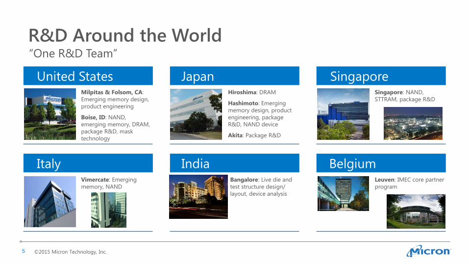
R&D Around the World“One R&D Team”
Milpitas & Folsom, CA:
Emerging memory design,
product engineering
Boise, ID: NAND,
emerging memory, DRAM,
package R&D, mask
technology
United States Japan Singapore
Italy India Belgium
Hiroshima: DRAM
Hashimoto: Emerging
memory design, product
engineering, package
R&D, NAND device
Akita: Package R&D
Singapore: NAND,
STTRAM, package R&D
Vimercate: Emerging
memory, NAND
Bangalore: Live die and
test structure design/
layout, device analysis
Leuven: IMEC core partner
program
©2015 Micron Technology, Inc.6
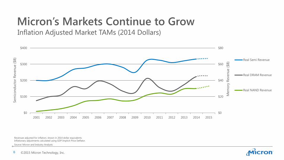
Micron’s Markets Continue to Grow
$0
$20
$40
$60
$80
$0
$100
$200
$300
$400
2001 2002 2003 2004 2005 2006 2007 2008 2009 2010 2011 2012 2013 2014 2015
Mem
ory
Reven
ue (
$B
)
Sem
ico
nd
uct
or
Reven
ue (
$B
)
Real Semi Revenue
Real DRAM Revenue
Real NAND Revenue
Inflation Adjusted Market TAMs (2014 Dollars)
Source: Micron and Industry Analysts
Revenues adjusted for inflation, shown in 2014 dollar equivalents.
Inflationary adjustments calculated using GDP Implicit Price Deflator.

©2015 Micron Technology, Inc.7
0
20
40
60
80
100
120
140
160
2015 2016 2017 2018 2019
DRAM Industry Bit Demand (B Gb EU)
Growing and Diversifying Memory Demand
Tablet
PC
Handset
AIMM
Consumer &
Graphics
Server/Storage/
Networking
Tablets contain a mix of mobile DRAM, standard DRAM, and reduced-power solutions. Upgrade modules included with PC.Source: Micron and Industry Analysts
0
50
100
150
200
250
300
350
2015 2016 2017 2018 2019
NAND Industry Bit Demand (B GB EU)
Tablet
Enterprise
SSD
Other
Removable
Storage
Handset
Client SSD
Consumer
Datacenter
SSD
©2015 Micron Technology, Inc.8
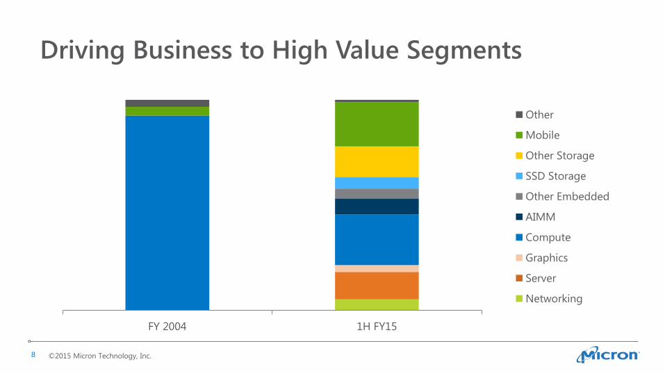
Driving Business to High Value Segments
Micron acquires Toshiba’s
commodity DRAM
operations
FY 2004 1H FY15
Other
Mobile
Other Storage
SSD Storage
Other Embedded
AIMM
Compute
Graphics
Server
Networking
©2015 Micron Technology, Inc.9
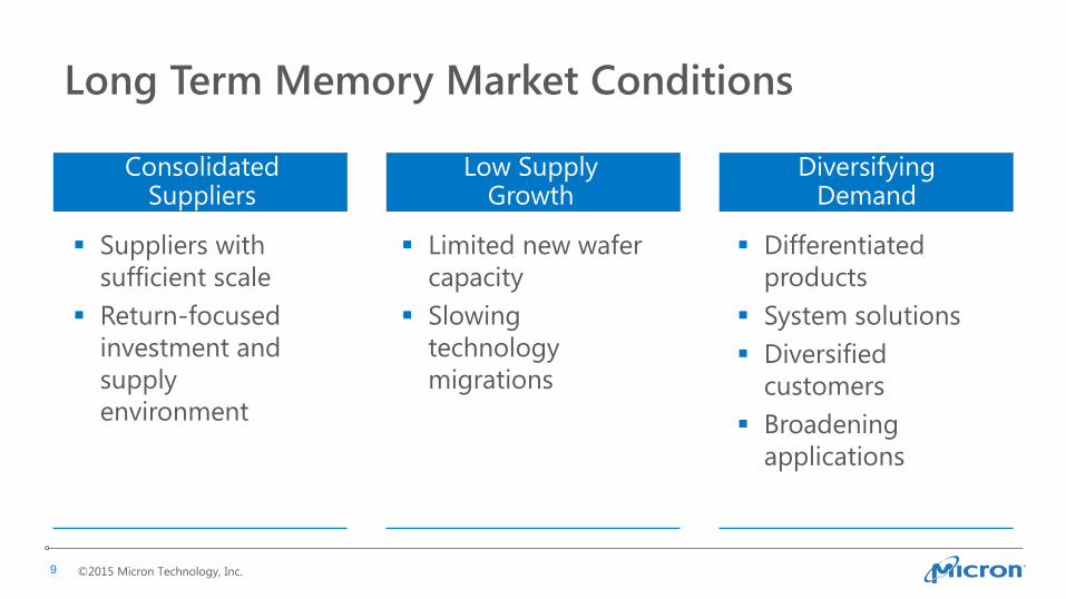
Long Term Memory Market Conditions
Suppliers with
sufficient scale
Return-focused
investment and
supply
environment
Limited new wafer
capacity
Slowing
technology
migrations
ConsolidatedSuppliers
Low Supply Growth
Differentiated
products
System solutions
Diversified
customers
Broadening
applications
DiversifyingDemand

©2015 Micron Technology, Inc.10
Trends and Challenges in Memory Innovation

©2015 Micron Technology, Inc.11
Micron’s Portfolio of Innovative “Firsts”DRAM 6F2 architecture
Leading DRAM capacitor technology
Copper metallization
Packaging (3Di) Hybrid memory cube, Through Silicon Via (TSV)
0.8mm four-layer LPDRAM package
NAND Pitch multiplication patterning
Award-winning, industry-leading
planar NAND cell technology
New Memory Productization of phase change memory
Demonstration of 16Gb resistive RAM
Development of 3D XPoint memory

©2015 Micron Technology, Inc.12
DRAM NAND New Memory Package
Edge yield improvements – continuous yield improvement
Ramp execution – new tool installs and matching, cost of transition
Process equipment maturity improvement: uniformity, capability
Defect detection and reduction
Development of new in-line characterization techniques to prevent
excursion, improve quality and yield
Development of
baseline 3Di
technology
Development of
first 3Di products
Challenges Faced in Technology Development
Continuous innovation in core process technology capability
©2015 Micron Technology, Inc.13
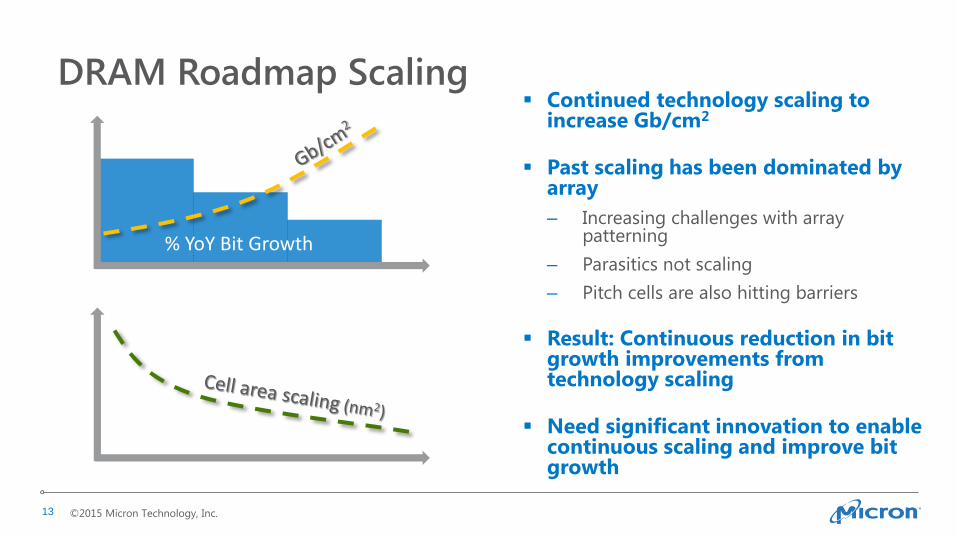
DRAM Roadmap Scaling Continued technology scaling to
increase Gb/cm2
Past scaling has been dominated by array
– Increasing challenges with array patterning
– Parasitics not scaling
– Pitch cells are also hitting barriers
Result: Continuous reduction in bit growth improvements from technology scaling
Need significant innovation to enable continuous scaling and improve bit growth
% YoY Bit Growth

©2015 Micron Technology, Inc.14
DRAM Scaling ChallengesARRAY (bottom of containers)
Cell Contact
Technology Node
Wtotal 6~7nm
Materials development required to improve array
efficiency and word line/bit line resistance
Capacitor structure
• Paradigm shift may be needed for cost effective scaling
Bit line and Word line
• Materials innovation required
Advanced device engineering
• To address materials/process limitations
Overlay and patterning demands
• May drive EUV adoption
Gap fill of narrow structures
• Need low T solutions
Advanced characterization
• HAR measurements, OCD

©2015 Micron Technology, Inc.15
NAND Roadmap Scaling
Planar NAND scaling
Planar NAND can still be scaled below 16nm, but performance & cost are not competitive with 3D
3D NAND scaling
3D NAND cost improvement over planar expands with subsequent nodes
3D cell architecture enables significant performance improvement relative to planar technology
25nm 20nm 16nm 1Znm 1Z'nm
32-tier TLC
48-tier TLC
64-tier TLC
96-tier TLC
GB
/cm
2
Technology Node
34nm
25nm
20nm 16nm 1Znm 1Z'nm
MU 32-tier MLC 32-tier TLC
48-tier TLC64-tier TLC
96-tier TLC
Co
st/G
B
Technology Node
3D NAND
3D NAND
PLANAR TLC
PLANAR TLC
Future Technology Projection
Future Cost Projection

©2015 Micron Technology, Inc.16
Vertical NAND Scaling Challenges
Tier Stack Scaling
High aspect ratio etch capability
Thin film deposition in high AR structures
Uniformity – WIW, WIF, WID, but also within localized high aspect
ratio structures
Advanced characterization – HAR measurements, OCD, embedded
defects and measurements
Staircase Contact Scaling
Advanced gap fill requirements for range of dimensions
Low temperature films deposition and treatment
Demanding Planarization
Thick film removal, new films, tighter uniformity specifications

©2015 Micron Technology, Inc.17
Packaging Technology Challenges
Development and deployment of baseline 3Di manufacturing processes
Transition from discrete-packaged memory to in-package memory
Thermal management of memory which shares a thermal solution with the ASIC or is inside the ASIC package
Control of warpage/coplanarity for ultra-thin dice used in ultra-thin packages
Accelerating development cycles, especially for market segments with short product life cycles
©2015 Micron Technology, Inc.18
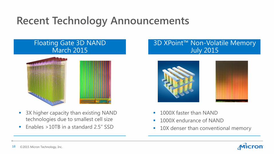
Recent Technology Announcements
3X higher capacity than existing NAND
technologies due to smallest cell size
Enables >10TB in a standard 2.5” SSD
1000X faster than NAND
1000X endurance of NAND
10X denser than conventional memory
Floating Gate 3D NAND March 2015
3D XPoint™ Non-Volatile MemoryJuly 2015
©2015 Micron Technology, Inc.19
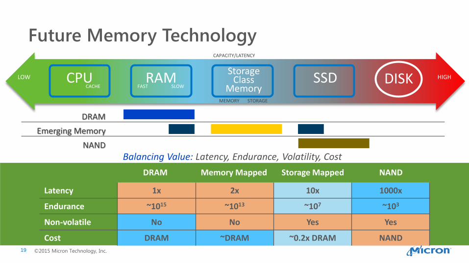
Future Memory Technology
DRAM
NAND
Balancing Value: Latency, Endurance, Volatility, Cost
Emerging Memory
LOW HIGHCPU RAM SSD DISKCACHE FAST SLOW
StorageClass
MemoryMEMORY STORAGE
Latency 1x 2x 10x 1000x
Endurance ~1015 ~1013 ~107 ~103
Non-volatile No No Yes Yes
Cost DRAM ~DRAM ~0.2x DRAM NAND
DRAM NANDMemory Mapped Storage Mapped
CAPACITY/LATENCY

©2015 Micron Technology, Inc.20
Polymers NanotubesNanowiresMagnetics
The Search for Successful New Memory Technology
It’s a great time to be a materials engineer!
W, TiN etc,.
Cu, Ag etc,.
+V -V Top lead
Free layer
Barrier
Fixed Layer
Antiferromagnet
Bottom lead
Cu/Ta
CoFeB
MgO
CoFeB
PtMn
Cu/Ta
MTJ
MTJ
Explosion of new memory concepts
Investigation focused on unique material
systems and product development
STT MRAMRRAM
PCM FeRAM
+

©2015 Micron Technology, Inc.21
Patterning with DSA: Challenges and Opportunities
©2015 Micron Technology, Inc.22
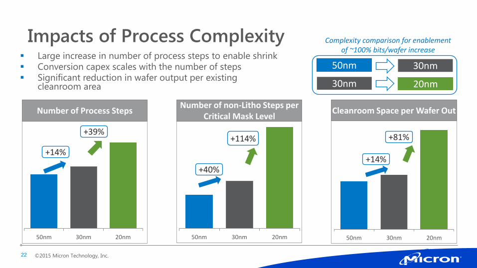
50nm 30nm 20nm
Impacts of Process Complexity Large increase in number of process steps to enable shrink
Conversion capex scales with the number of steps Significant reduction in wafer output per existing
cleanroom area
Number of Process Steps Cleanroom Space per Wafer Out
50nm 30nm 20nm
+14%
+39%
+14%
+81%
50nm 30nm 20nm
Number of non-Litho Steps per Critical Mask Level
+40%
+114%
Complexity comparison for enablementof ~100% bits/wafer increase
50nm
30nm
30nm
20nm
©2015 Micron Technology, Inc.23
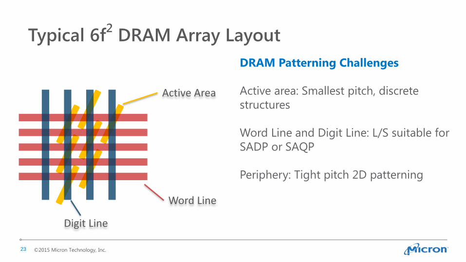
Active Area
Typical 6f2
DRAM Array Layout
Word Line
Digit Line
DRAM Patterning Challenges
Active area: Smallest pitch, discrete
structures
Word Line and Digit Line: L/S suitable for
SADP or SAQP
Periphery: Tight pitch 2D patterning

©2015 Micron Technology, Inc.24
Active Area Patterning
Dense lines are initially formed
by SADP or SAQP
Lines are then chopped to create
islands
Contact chop pattern
1Ynm – 1Znm LELE
Beyond 1Znm, EUV
Option (1Znm and beyond)
High NA, EUV, single print
DSA has an opportunity to
replace SAQP for dense line
patterning, when ready and
cost competitive
©2015 Micron Technology, Inc.25
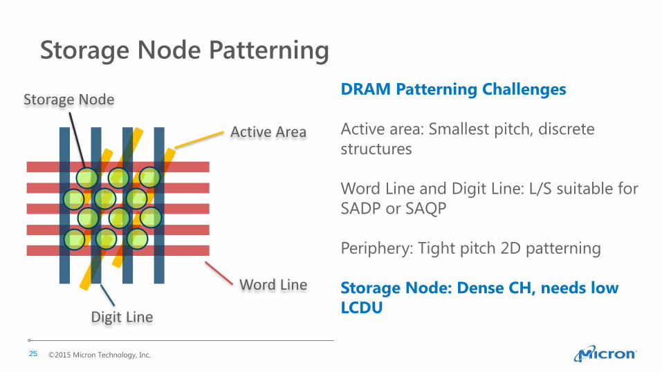
Active Area
Storage Node Patterning
Word Line
Digit Line
Storage NodeDRAM Patterning Challenges
Active area: Smallest pitch, discrete
structures
Word Line and Digit Line: L/S suitable for
SADP or SAQP
Periphery: Tight pitch 2D patterning
Storage Node: Dense CH, needs low
LCDU

©2015 Micron Technology, Inc.26
Storage Node Patterning
Main challenge is local
CD uniformity
CD uniformity needs
improvement for
single patterning
Potential path but need
to address LCDU,
defects, placement error
ArF Immersion EUV DSA CHIPS Flow
©2015 Micron Technology, Inc.27
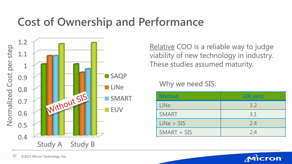
Cost of Ownership and Performance
0.4
0.5
0.6
0.7
0.8
0.9
1
1.1
1.2
SAQP
LiNe
SMART
EUV
Method LER (nm)
LiNe 3.2
SMART 3.1
LiNe + SIS 2.4
SMART + SIS 2.4
No
rmalize
d C
ost
per
step
Study A Study B
Why we need SIS:
Relative COO is a reliable way to judge
viability of new technology in industry.
These studies assumed maturity.

©2015 Micron Technology, Inc.28
DSA Adoption Challenges
Defectivity
Needs to improve by a few orders of magnitude
Pattern roughness
Needs to be comparable or better than SAQP
SIS and other post processing may help, but add cost, complexity and potentially
defectivity
Process/Integration complexity
Pattern placement error and overlay issues need to be further studied
Integration issues such as termination, edge of array, etch, alignment and overlay
marks
Cost
Cost advantage over SAQP needs to be significant

©2015 Micron Technology, Inc.29
Highlights
Exciting time for memory: diversifying markets, new applications
Lots of challenges ahead in both silicon processing and package development
Winning patterning technologies have to win for performance and cost
Trend is 3D and materials innovation
1
2
3
4

©2015 Micron Technology, Inc.30
Thank You

©2015 Micron Technology, Inc.31