memory organization
TRANSCRIPT


1. LocationComputer memory is placed in 3 different locations :a. Processor (CPU) : In the form of CPU registers and it’s internal
cache memory.b. Internal (Main Memory) : Main memory which the CPU directly
accesses. c. External (Secondary memory) : Secondary memory devices like
the magnetis disk, tapes.2. Capacity : Expressed as word size and no. of words.Common word sizes are 8, 16,32, 64 bits.No. of words specifies the no. of words available in a particular memory.Memory Capacity = 4 K x 8 = (4 x 1024 ) x 8 bits=32768 bits
no. of wordsword size
3. Unit of transferInternal(MM)
◦ Usually governed by data bus widthExternal(secondary)
◦ Usually a block which is much larger than a word

4. Access type• Sequential – tapeo Start at the beginning and read through in ordero Access time depends on location of data and previous
location• Direct – disko Individual blocks have unique addresso Access is by jumping to vicinity plus sequential search• Random - RAMo Individual addresses identify location exactly

5. Performance : 3 performance parameters are: • Access time (latency)The time between presenting an address and getting access to valid data• Memory Cycle time Consists of access time plus any additional time required before second access can begin =Access time plus recovery time• Transfer rateThe rate at which data can be transferred into or out of a
memory unit

6. Physical type
Semiconductor – RAM Magnetic – disk and tape Optical – CD and DVD
7. Physical CharacteristicsVolatile/non-volatileVolatile : Information is lost when power is switched off ( eg.
RAM)Non-volatile : Magnetic Tapes/Disks.

Semi Conductor Memories
Read Only memory(ROM) Random Access Memory
Non volatile memory Used to store system level programs (Eg BIOS)
PROM UV-EPROM EEPROM Static RAM(SRAM) Dynamic RAM(DRAM)

Programmable ROM• One-time programmable non-volatile memory (OTP NVM) Erasable PROM • Possible to erase information on the ROM chip by exposing the
chip to UV light.• The chip has to be physically removed from the circuit to erase
the info. Electrically Erasable PROM• ROM that can be erased and reprogrammed (written to)
repeatedly through the application electrical voltage .• Chip does not have to be removed for erasure.
RAM :• Contents are lost when power is turned off.• Volatile memory.• Types – SRAM and DRAMa) DRAM :• Stores each bit of data in a separate capacitor.• Hence information can be stored only for a few milliseconds.• To store information for a longer time, contents of the capacitor
needs to be refreshed periodically.• Hence this makes DRAMs slower.• Used to implement main memory.• Cheaper

b) SRAM :• Each bit in an SRAM is stored on four transistors.• Hence a low density device compared to DRAM.• No capacitors are used hence no refreshing required.• Hence faster as compared to DRAMs• Expensive.• Used in cache memories.

SRAM DRAM
Transistors used to store info.
Capacitors are used to store data.
No refreshing required. Refreshing is required.
Fast Memory Slower memory
Expensive Cheaper
Low density device High density device
Used in Cache memories Used in main memories

Processor
Registers
Primary cache L1
Secondary cache L2
Main Memory
Secondary Memory(Magnetic disk, CDROM)
Increasing size Increasing
speedIncreasing cost/bit

Processor fetches the code and data from main memory (MM). MM is implemented using DRAM which are slower devices. This reduces the speed of execution.Soln : At a time a program works only on a small section of code and data. Hence add a small section of SRAM along with DRAM which is
referred to as a cache memory.1. Registers: The fastest access to data is to data held in processor registers.Eg: Program counter, SP , general purpose registers.2. Level 1 cache ( L1 or primary cache) : Small amount of memory implemented directly on the processor chip called processor cache.Holds copies of of instructions and data stored in a much larger memory.Implementation – Using SRAM chips.
3. Level 2 cache (L2- secondary cache)Placed between the primary cache and the rest of the memory.Implementation – Using SRAM chips.
4. Main memory Larger but slower than cache memory.Access time (MM) = 10 times access time of L1 cache.Implementation – Using DRAM chips.
5. Secondary memoryProvides huge amount of inexpensive storage.Slower compared to semiconductor memories.Hold programs and data not continually required by the CPU.

Main memory consists of 2n addressable words each word having a unique n-bit address.
MM is divided into blocks of k words each. Total no. of blocks (M) = 2n / K Cache consists of C lines of k words each ( C<<
M) At any time, some subset of the blocks of main
memory resides in the lines in the cache.

Tag identifies which particular block of MM is currently stored in the cache.

Assume 4 bit address line. 24 = 16 possible addresses. Each address stores 1 word (Assume 1 word = 1 byte) Hence total main memory capacity= 16 bytes Assume block size = 2 words Hence total no. of blocks =24/2 = 8 blocks.
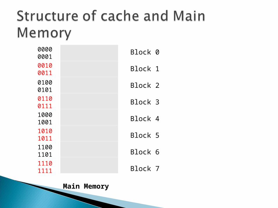
Block 0
Block 1
Block 2
Block 3
Block 4
Block 5
Block 6
Block 7
0000000100100011
010001010110011110001001101010111100110111101111
Main Memory

Cache memory – Small amount of fast memory placed between processor and main memory

Cache memory overview• Processor requests the contents of some memory
location(word).• The cache is checked for the requested data.• If found, the requested word is delivered to the processor.• If not found, the block of MM in which the word resides is
read into the cache and the requested word is delivered to the processor.
• A block of data is bought into the cache even though the processor requires only a word in that block since it is likely that there will be future references to the same memory location(word) or to other words in the block. This is called the locality of reference principle

It is observed that memory reference by the processor for data and instructions cluster.
Programs contain iterative loops and subroutines . Once a loop is entered , there are repeated references to a small set of instructions.
Operations on tables and arrays involve access to a clustered set of data words.

2 ways of introducing cache into a computer :1. Look aside cache design2. Look through cache design

1. Look aside cache design
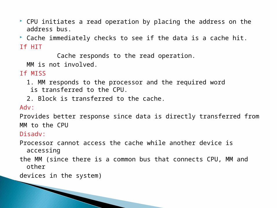
CPU initiates a read operation by placing the address on the address bus.
Cache immediately checks to see if the data is a cache hit.If HIT Cache responds to the read operation.
MM is not involved.If MISS
1. MM responds to the processor and the required word is transferred to the CPU.2. Block is transferred to the cache.
Adv:Provides better response since data is directly transferred fromMM to the CPUDisadv:Processor cannot access the cache while another device is accessing the MM (since there is a common bus that connects CPU, MM and
other devices in the system)
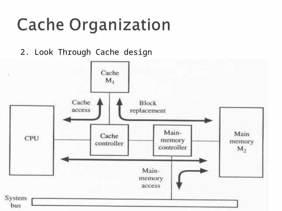
2. Look Through Cache design

CPU communicates with the cache via a local bus isolated from the system bus.
The CPU initiates a read operation by checking if data is in cache.
If HIT Cache responds to the read operation.MM is not involved.
If MISS1. Block is first read into cache.2. Word is transferred from cache to the processor.

1. Cache size Minimize the cache size. Larger is cache, larger is the no of gates involved in addressing
the cache, as a result performance decreases i.e. cache becomes slower.
2. Mapping Function Fewer cache lines than MM blocks. Hence an algorithm is required to map main memory blocks into
cache lines. 3 techniques used are :1. Direct mapping2. Associative mapping3. Set Associative mapping

1. Direct mappingNo. of bits in MM address = 4 bits. Hence 16 possible addresses.
Cache size = 8 bytes.Block size = 2 bytes(2 words). Assume 1 Word = 1 ByteHence total no. of cache lines = 8/2 = 4
Main memory address is split as-----
Tag
0
1
2
3
Line No.
T A G L I N E W O R D

1. No. of bits in the WORD field :
No. of bits in Word field depends on the block size. Since Blk size = 2 Words. Hence Word field is 1 bit.
2. No. of bits in the LINE field :
No. of bits in Line field depends on the no. of cache lines. Since no. of cache lines = 4 Hence Line field is 2 bit.
3. No. of bits in the TAG field :Remaining 1 bit for TAG since (4-(2+1))=1
1 2 1
MM address

A block of MM goes to block no.(i) mod total no. of lines in cache(c)i.e. i mod cBlock 5 of MM will go to 5 mod 4 =1 i.e. line 1 of cache
Tag
0
2
3
Line No.
1 Block 51

How does the cpu access data from the cache ? i.e if the cpu needs data at address 1011
Tag Line Word
1. Line is used as an index into the cache to access particular line.
2. If the 1-bit tag no. in the address matches the tag no. stored currently in that line then 1-bit word is used to select one of the 2 words in that line.
3. Otherwise the 3 bit (Tag + line) field is used to fetch the block from the main memory.
1 0 1 1

Computer has a 32 bit MM add. SpaceCache size= 8KBBlock size =16 bytesSince each block is of 16 bytes hence 4 bits in the WORD
field.28 bits for TAG and LINE.Cache size is 8KBNo. of cache lines = 8KB/16= 512 lines512 = 29
Hence 9 bits for the LINE field.Hence TAG = 19 bits
19 9 4
32 bits of MM address

EgCache
0123
511
Block0Block1Block2
Block512

Adv :Cache controller quickly releases hit/miss information.Diasdv :Not flexible because a given block is mapped onto a fixed cache line.

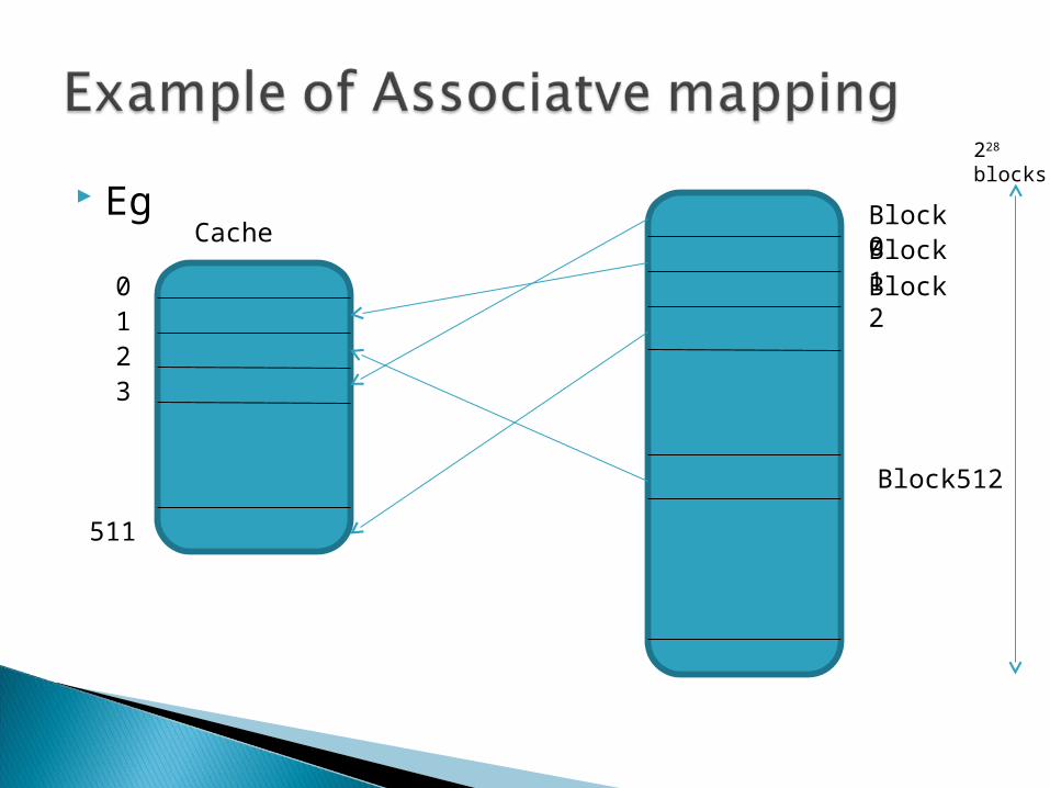
2. Associative mapping Best and most expensive. A block of MM can be mapped to any cache line. MM address consists of 2 fields
When the CPU needs a word, the cache controller has to match the TAG field in the address with the TAG contents of all the lines in cache.
Adv: Offers flexibility since a block of MM can be moved to any cache line. Hence replacement is needed only if cache is totally full.Diadv:
Longer access time
T A G W O R D

No. of bits in the WORD field :No. of bits in Word field depends on the block size. No. of bits in the TAG field :Total no. of bits in MM address – No. of bits in WORD field
Computer has a 32 bit MM add. SpaceCache size= 8KBBlock size =16 bytes
Since each block is of 16 bytes hence 4 bits in the WORD field.
Remaining 28 bits for the TAG
T A G W O R D
28 4
EgCache
0123
511
Block0Block1Block2
Block512
228
blocks

3. Set associative mapping Combination of direct mapping and associative mapping. Cache is divided into v sets consisting of k lines each. Hence total lines in cache = v x k
Total no. sets No.of lines in each set K lines in each set ---- Called k-way set associative MM block can be mapped into a specific set only. Which set?
Block i of MM gets mapped into set -- i mod v Within a set a block can be placed in any line. MM address has 3 fields
T A G S E T W O R D

No. of bits in the WORD field :No. of bits in Word field depends on the block size. No. of bits in the SET field :No. of bits in Set field depends on the number of sets. No. of bits in the TAG field :Total no. of bits in MM address – (No. of bits in WORD field + No. of bits in Set field )
When the CPU needs to check the cache for accessing a word, the cache controller uses the SET field to access the cache.
Within the set there are k lines, hence the TAG field in address is matched with TAG contents of all k lines.

Computer has a 32 bit MM add. spaceCache size= 8KBBlock size =16 bytes4 way set associative.
No. of cache lines = 8KB/16= 512 lines Total no. of sets =512/4 =128 = 27
Hence no. of bits in SET = 7No. of bits in WORD = 4No. of bits in TAG = 21
T A G S E T W O R D
21 7 4

EgCache
0123
Block0Block1Block2
Block512
228
blocks
Set0
Set1
Set128

Adv: Flexible compared to Direct mapping. Multiple choices for mapping a MM block . No. of options depend on k. During searching , TAG matching is limited to the no. of
lines in the set.

2. Cache can hold 64KB of data.Data is transferred between MM and the cache in blocks of 4 bytes each.MM consists of 16MB.Find the distribution of MM address in all 3 mapping techniques.
1. Direct MappingSince MM consists of 16MB.24 x 220 = 224
i.e 224 locations (addresses)Hence no. of bits in MM address is 24.No. of cache lines= 26 x 210 / 22 = 214
To select one of the cache line 14 bits are required.LINE = 14 bits, WORD = 2 ( since block size = 4 bytes)
TAG= 24-(14+2)=8

2. Associative MappingMM address
Word = 2 bits ( since block size = 4 bytes)TAG= 24-2 =22 bits
T A G W O R D
22 2

3. Set Associative MappingAssume 2 way set associativei.e 2 cache lines make 1 set.MM add.
Hence no. of sets =214/2 = 213
To select 1 of the 213 sets we require 13 bits.Hence no. of bits in SET field =13.Hence no. of bits in WORD field =2.Hence no. of bits in TAG field =24-(13+2) =9
9 13 2
T A G S E T W O R D
T A G S E T W O R D

Eg:A set associative cache consists of 64 lines, divided into 4-line sets. MM consists 4K blocks of 128 words each. Show the format of MM addess.No. of blocks in MM = 4K= 210 x 22 = 212
Total no. of words in MM = 212 x 128 = 219
Hence total no. of bits in MM address =19 bits.Total no. of lines in cache= 64Total no. of sets in cache=64/4= 16= 24
Hence total no. of bits in SET field = 4.Block size = 128 words= 27
Hence total no. of bits in Word field = 7.Tag =19-(7+ 4) =8
8 4 7
T A G S E T W O R D
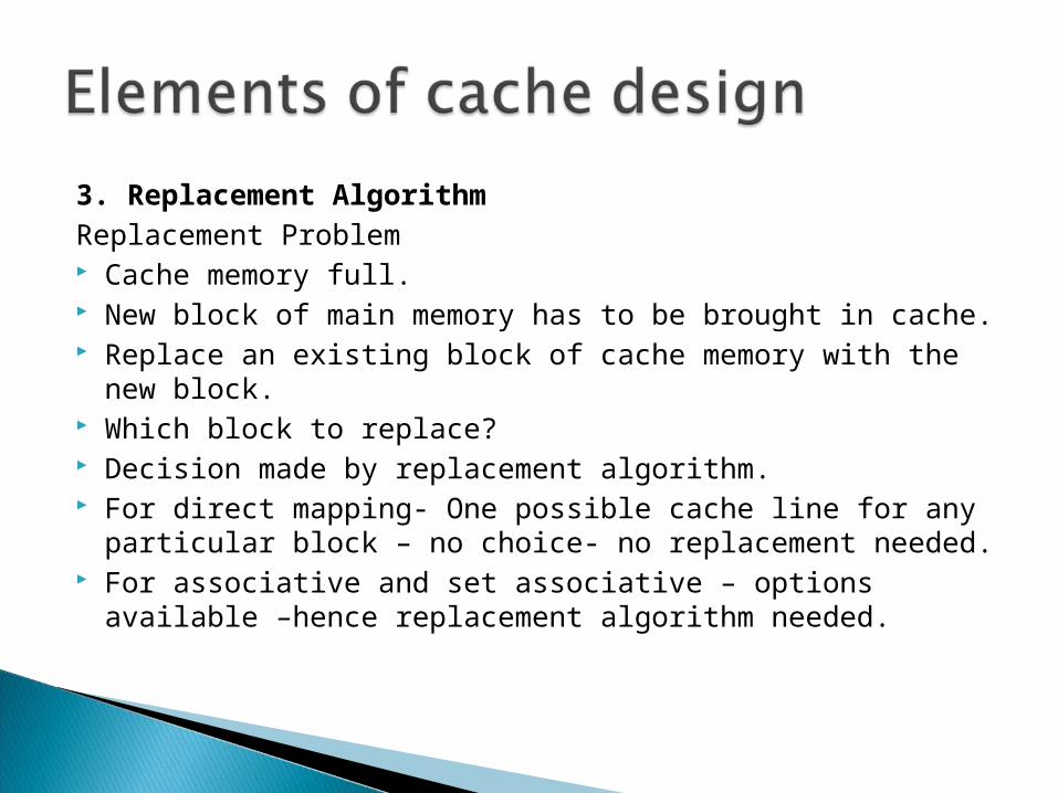
3. Replacement AlgorithmReplacement Problem Cache memory full. New block of main memory has to be brought in cache. Replace an existing block of cache memory with the new
block. Which block to replace? Decision made by replacement algorithm. For direct mapping- One possible cache line for any
particular block – no choice- no replacement needed. For associative and set associative – options available –
hence replacement algorithm needed.

4 common replacement algorithms used :1. Least recently used(LRU):
Replace the line in the cache that has been in the cache the longest with no reference to it. Since it is assumed that the more recently used blocks are more likely to be referenced again.Can be implemented easily in a 2-way set associative mapping.Each line includes a USE bit.
When line is referenced it’s USE bit is set to 1 and the USE bit of the other line in that set is set to 0.When set is full, consider that block for replacement whose USE bit is zero.

2. First In First Out :Replace the block that has been in the cache the longest.3.Least Frequently used (LFU)Replace the block that has had the least references. Requires a counter for each cache line.4. Random AlgorithmRandomly replace a line in the cache.
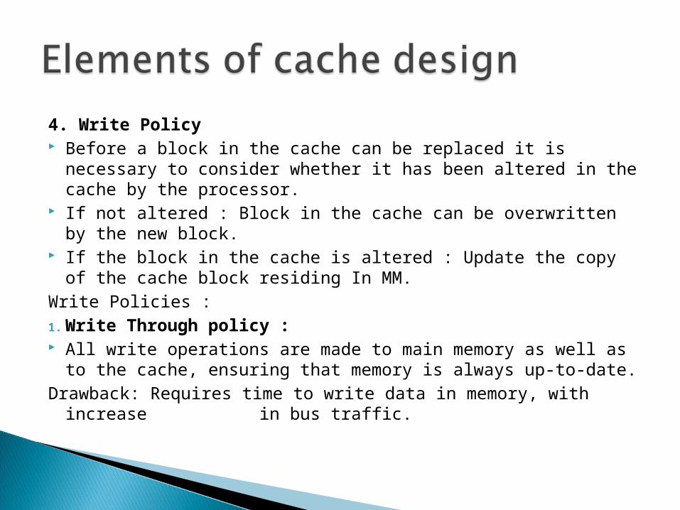
4. Write Policy Before a block in the cache can be replaced it is necessary to
consider whether it has been altered in the cache by the processor.
If not altered : Block in the cache can be overwritten by the new block.
If the block in the cache is altered : Update the copy of the cache block residing In MM.
Write Policies :1. Write Through policy : All write operations are made to main memory as well as to
the cache, ensuring that memory is always up-to-date.Drawback: Requires time to write data in memory, with
increase in bus traffic.

2. Write back Policy/Copy back policy Updates are made only to the copy of the block in cache
and not to the copy of block in MM. Update bit is associated with each line which is set when
the block in the cache is updated. When a block in cache is considered for replacement, it is
written back in MM if and only if the UPDATE bit is set. Minimizes MM writes
Adv: Saves time since writing in MM is not done for every write operation on cache block.

3. Buffered write through : Improvement of write through policy. When an update is made to a cache block the update is
also written into a buffer and from the buffer updates are made to the MM.
Processor can start a new write cycle to the cache before the previous write cycle to MM is completed since writes to MM are buffered.

Cache coherency: Cache coherence problem occurs in a multiprocessor system. There are multiple processors, each processor has it’s own
cache with a common memory. Due to the presence of multiple caches, copies of 1 MM block
can be present in multiple caches. When any processor writes(updates) a word in it’s own cache,
all other caches that contain a copy of that word will have the old, incorrect value.
Hence the caches that contain a copy of that word must be informed of the change.
Cache coherence problem occurs when a processor modifies it’s cache without making the updates available to other caches.

Cache Coherence is defined as a condition in which all the cache blocks of a shared memory block contain same information at any point of time.

Apr 18, 2023CPE 731, Snooping 55
◦ Processors see different values for u after event 3◦ Write done by P3 not visible to P1,P2
I/O devices
Memory
P1
cache cache cache
P2 P3
5
u = ?
4
u = ?
u :51
u :5
2
u :5
3
u = 7
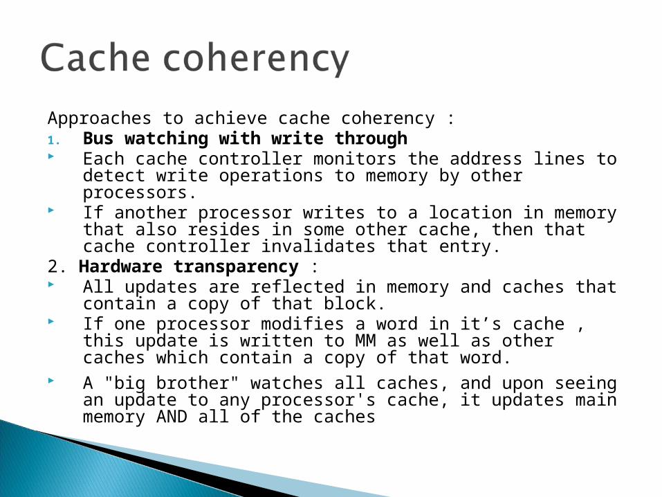
Approaches to achieve cache coherency :1. Bus watching with write through Each cache controller monitors the address lines to
detect write operations to memory by other processors. If another processor writes to a location in memory that
also resides in some other cache, then that cache controller invalidates that entry.
2. Hardware transparency : All updates are reflected in memory and caches that
contain a copy of that block. If one processor modifies a word in it’s cache , this
update is written to MM as well as other caches which contain a copy of that word.
A "big brother" watches all caches, and upon seeing an update to any processor's cache, it updates main memory AND all of the caches
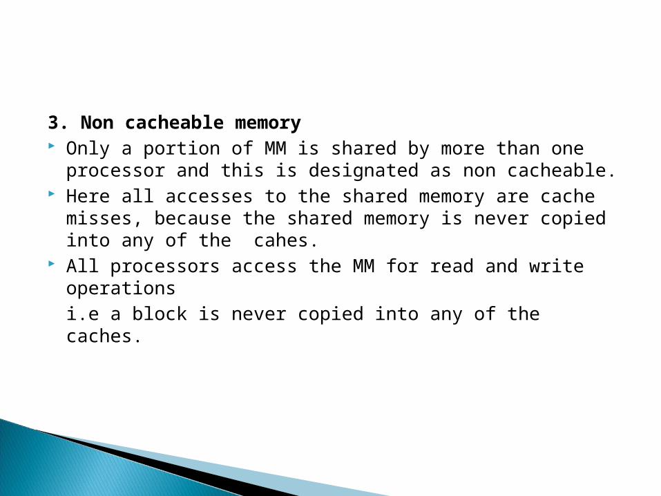
3. Non cacheable memory Only a portion of MM is shared by more than one processor
and this is designated as non cacheable. Here all accesses to the shared memory are cache misses,
because the shared memory is never copied into any of the cahes.
All processors access the MM for read and write operations i.e a block is never copied into any of the caches.

5. Line Size(Block size) As block size increases from very small to larger sizes , hit ration
increases due to principle of locality. However as blocks become even bigger hit ration decreases since :1. Larger blocks reduce the no. of blocks that fit into cache.2. As blocks become larger , each additional word is farther away
from the requested word and therefore less likely to be needed in the near future.
6. No. of caches :1. Single/two levelOriginally a typical system has a single cache. Recently multiple caches has become the norm.Multilevel caches2- level caches - L1 and L2 cache.

2. Unified/Split cachesUnified cache: Single cache is used to store data and Instructions.Split cache : Split the cache into two. One dedicated for
instructions and the other dedicated for data.

Main memory is divided into 2 parts :one for the operating system and the other part for user programs.
In uniprogramming, there is OS in one part and the other part for the program currently being executed.
In a multi programming system, the user part of the memory must be further subdivided to accommodate multiple processes.
One of the basic functions of the OS is to bring processes into main memory for execution by the processor.

1. Multiprogramming with Fixed Partitions (Multiprogramming with Fixed number of tasks-MFT)
Obsolete technique. Supports multiprogramming. Based on contiguous allocation. Memory is partitioned into fixed number of partitions but their size remains fixed. The first region is reserved for the OS and the remaining partitions are used for the user programs.

An example of a partitioned memory : Memory is partitioned into 5 regions. The
first is reserved for the OS.
Partition Starting add of partition
Size of partition
Status
1 0K 200 K ALLOCATED
2 200 K 100 K FREE
3 300 K 150 K FREE
4 450 k 250 K ALLOCATED
5 700 K 300 K FREE

Once partitions are defined , the OS keeps track of the status of each partition (allocated/free) through a data structure called PARTITION TABLE.
For execution of a program, it is assigned to a partition. Partition should be large enough to accommodate the program to be executed.
After allocation some memory in the partition may remain unused. This is known as internal fragmentation.

Strategies used to allocate free partition to a program are:
1. First –fit : Allocates the first free partition large enough to accommodate the process.
Leads to fast allocation of memory space.2. Best- fit
Allocates the smallest free partition that can accommodate the process. Results in least wasted space Internal fragmentation reduced but not
eliminated

3. Worst fitAllocates the largest free partition that can accommodate the process
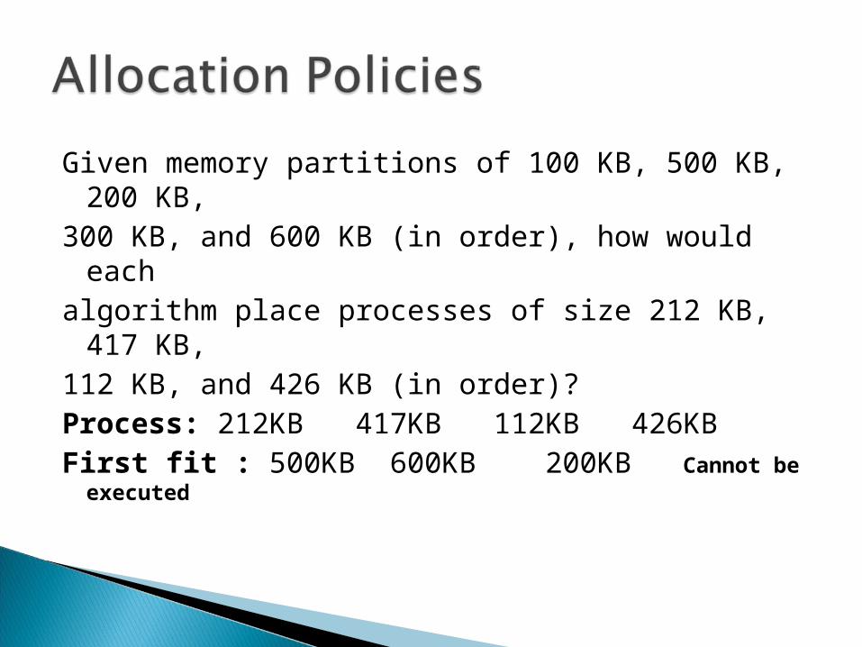
Given memory partitions of 100 KB, 500 KB, 200 KB,
300 KB, and 600 KB (in order), how would each algorithm place processes of size 212 KB, 417 KB, 112 KB, and 426 KB (in order)?Process: 212KB 417KB 112KB 426KBFirst fit : 500KB 600KB 200KB Cannot be
executed
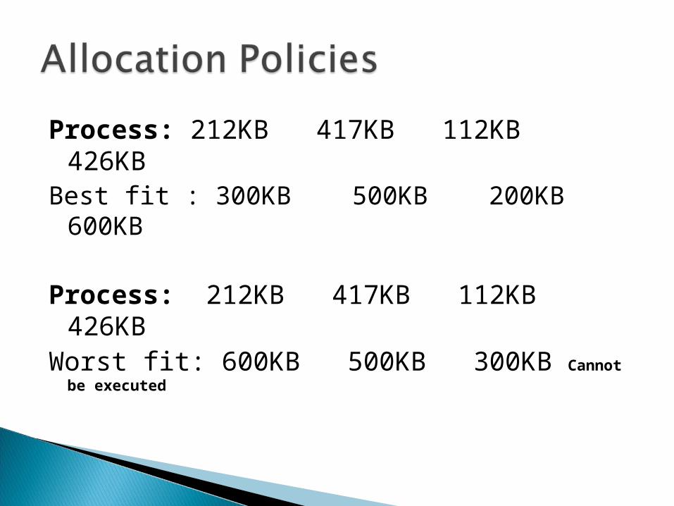
Process: 212KB 417KB 112KB 426KBBest fit : 300KB 500KB 200KB 600KB
Process: 212KB 417KB 112KB 426KBWorst fit: 600KB 500KB 300KB Cannot be
executed

Disadvantage of MFT : The number of active processes is limited
by the system i.e. limited by the pre-determined number of
partitions A large number of very small process will
not use the space efficiently giving rise to internal fragmentation.

2. Dynamic Partitioning (Multprogramming with variable no. of tasks-MVT)
Developed to overcome the difficulties with fixed Partitioning. Partitions are of variable length and number dictated by the size
of the process. A process is allocated exactly as much memory as required. Eg: 64 MB of MM. Initially MM is empty except for the OS

Process 1 arrives of size 20 M.Next process 2 arrives of size 14 M.Next process 3 arrives of size 18 M.
Hole at the end of the memory of 4 M that is too small for process 4 of 8 M

•Process 2 finishes execution

Process 4 is loaded creating another small hole of 6 M

•Process 1 finishes execution on CPU.•Process 5 of 14 M comes in.

MVT eventually leads to a situation in which there are a lot of small holes in memory.
This is called external fragmentation.External fragmentation – total memory
space exists to satisfy a request, but it is not contiguous; storage is fragmented into a large number of small holes.

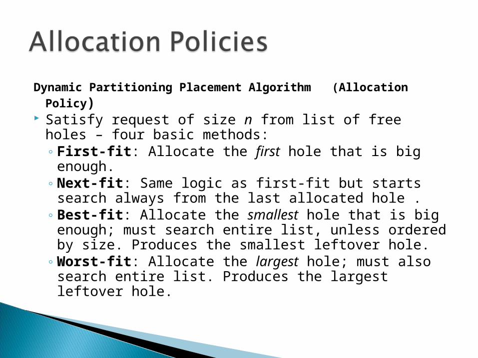
Dynamic Partitioning Placement Algorithm (Allocation Policy)
Satisfy request of size n from list of free holes – four basic methods:◦First-fit: Allocate the first hole that is big enough.◦Next-fit: Same logic as first-fit but starts search
always from the last allocated hole . ◦Best-fit: Allocate the smallest hole that is big
enough; must search entire list, unless ordered by size. Produces the smallest leftover hole.
◦Worst-fit: Allocate the largest hole; must also search entire list. Produces the largest leftover hole.

Last block that was used was a 22 MB block, from which 14 MB was used by the process returning a hole of 8MBAssuming now a program of size 16 MB had to be allocated memory.

Issues in modern computer systems: Physical main memory is not as large as the size of the user
programs. In a multiprogramming environment more than 1 programs are
competing to be in MM. Size of each is larger than the size of MM.Solution : Parts of the program currently required by the processor are brought into the MM and remaining stored on the secondary devices. Movement of programs and data between secondary storage and MM is handled by the OS. User does not need to be aware of limitations imposed by the
available memory.

Def: Virtual memory VM is a concept which enables a program to execute even
when it’s entire code and data are not present in memory. Permits execution of a program whose size exceeds the
size of the MM. VM is a concept implemented through a technique called
paging.
Paging Logical address : Location relative to the beginning of a
program Physical address : Actual locations in Main memory. Cpu when executing a program is aware of only the logical
addresses.

When a program needs to be accessed from the MM, MM should be presented with physical addresses.
Memory Management Unit (MMU) converts the logical addresses into physical addresses.
A memory management unit (MMU), is a computer hardware component responsible
for converting the logical add. to physical add. In paging scheme --User programs are split into fixed sized blocks called pages.Physical memory is also divided into fixed size slots called page frames.Page size --- 512 bytes, 1 K, 2K ,8K in length.Allocation of memory to a program consists of finding a sufficient no. of unused frames for loading of pages of a
program.Each page requires one page frame.

Logical Address
Lower order n bits designate the offset within the page.Higher order (m-n) bits designate the page no.
Page no. Offset
m bits
n bits

How user programs are mapped into physical memory?
abcd
Ijkl
mnop
Logical Memory (user program)
1
0
2
3
0
1
2
3
4
5
6
7
8
9
10
11
12
13
14
15
efgh
.
.
Frame 0
Frame 1
Frame 2
Frame 3
Frame n-1
Let the logical memory of a program be 2m bytes
Hence no. of bits in the logical address is m bits.Here m= 4 bits
Size of a page be 2n bytes.
Logical address
Page no. Offset
m bits
n bits

Paging Example - 32-byte memory with 4-byte pages
abcd
efgh
Ijkl
mnop
0 51 62 13 2
Page Table
Logical Memory
I j k l
m n op
a b cd
ef
g h
Physical Memory
Virtual Memory: Paging
1
1
2
3
4
5
6
7
0
Frame 0
2
3
0
1
2
3
4
5
6
7
8
9
10
11
12
13
14
15
Gives information that a page is in which page frame

Mapping from logical address to physical address-Assume CPU wants to access data corresponding to logical Address 14 :
1. Use page no. field (11) to index into the page table (PT)2. Indexing the PT we find page 3 is in frame no. 2 of MM.3. 2 x 4(page size) =84. 8 - base address of frame 25. Use the offset of the logical address to access the byte
within the frame. Offset - 10(2)6. 8 + 2(offset) = 10Hence logical address 14 maps to physical address 10
1 1 1 0
Page no. Offset

PagingPaging

At a given point in time, some of the frames ain memory are in use and some are free

Do not load all pages of a program in memory, put some pages in memory which will be required and other pages are kept on the backing store (secondary memory)
Structue of a page table
Page No
Frame No.
Valid Dirty bit
0 5 1 1
1 2 1 0
2 3 1 1
3 - 0 0
4 - 0 0
Valid bit – Indicates whether a page is actually loaded in main memory.
Dirty bit – Indicates whether the page has been modified during it’s residency in the main memory

What happens when the CPU tries to use a page that was not brought into the memory ?1. The MMU tries to translate the logical address into physical
address by using the page table.2. During the translation procedure, the page no. of the logical
address is used to index the PT. The valid bit for that page table entry is checked to indicate whether the page is in memory or not.
3. If bit =0 then page is not in memory, and it is a page fault which causes an interrupt to the OS. i.e a request for a page that is not in MM.
4. OS searches MM to find a free frame to bring in the required page.5. Disk operation is scheduled to bring in the desired page into the
newly allocated frame.6. Page table is modified to indicate that the page is in MM.7. MMU uses the modified PT to translate the logical address to
physical adress.
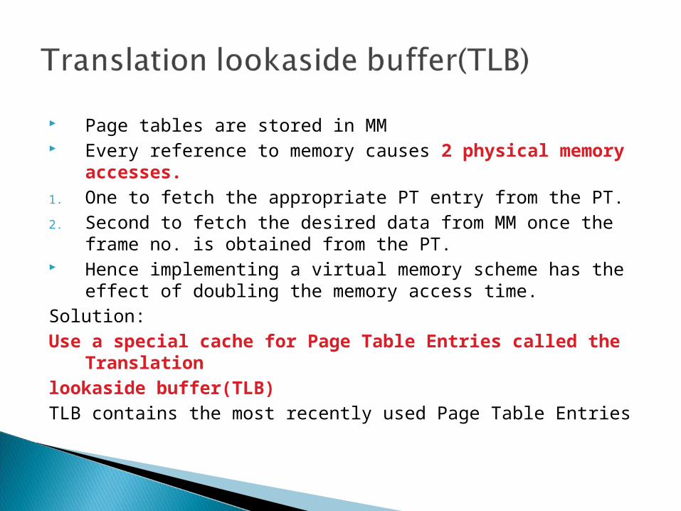
Page tables are stored in MM Every reference to memory causes 2 physical memory
accesses.1. One to fetch the appropriate PT entry from the PT.2. Second to fetch the desired data from MM once the frame
no. is obtained from the PT. Hence implementing a virtual memory scheme has the
effect of doubling the memory access time.Solution:Use a special cache for Page Table Entries called the
Translation lookaside buffer(TLB)TLB contains the most recently used Page Table Entries

Operation of paging using a TLB:1. Logical address is in the form
2. During the translation Process MMU consults the TLB to see if the matching Page table entry is present.
3. If match found, physical address is generarted by combining the frame no. present at that entry at that entry in the TLB with the offset.
4. If match not found, entry is accessed from the page table in the memory.
Page no. Offset


When MM is full page replacement algorithm determines which page in memory will be replaced to bring in the new page.
1. First-In-First-Out (FIFO) Replaces the oldest page in memory i.e the page that has
spent longest time in memory. Implemented using a FIFO queue. Replace the page at
the head of the queue.

Assume MM has 3 page frames. Execution of a program requires 5 distinct pages Pi where i= 1,2,3,4,5
Let the reference string be2 3 2 1 5 2 4 5 3 2 5 2
5
3
1
2 2
3
2
3
2
3
1
3
2
4
5
2
1
5
2
4
5
2
4
3
2
4
3
5
2
3
5
4
HH HHit ratio = 3/12
Drawback: Tends to throw away frequently used pages because it does not take into account the pattern of usage of a given page

Least Recently used Algorithm : Replaces that page which has not been used for the
longest period of time.
2 3 2 1 5 2 4 5 3 2 5 2
2
5
1
2 2
3
2
3
2
3
1
3
5
2
2
5
1
2
5
4
2
5
4
3
5
4
3
5
2
3
5
2
HH H H H
No. of page faults =7
Hit ratio = 5/12
Generates less no. of page faults than FIFO
Commonly used algorithms

3. Optimal page Replacement algorithm Replace that page which will not be used for the longest
period of time.2 3 2 1 5 2 4 5 3 2 5 2
2
3
5
2 2
3
2
3
2
3
1
2
3
5
2
3
5
4
3
5
4
3
5
4
3
5
2
3
5
2
3
5
HH H H HH
Hit Ratio=6/12=1/2
Drawback: Difficult to implement since it requires a future knowledge of the reference string.
Used mainly for comparison studies.

Reference String : 7 0 1 2 0 3 0 4 2 3 0Assume no. of page frames =3FIFO
H
Hit ratio = 1/11

LRU
Hit ratio = 2/11
H H

Optimal
H H HH
Hit ratio = 4/11

Assumption: 2 level memory- cache, MM This 2 level memory provides improved performance over 1
level memory due to a property called locality of reference 2 types of locality of reference ;1. Spatial locality : Tendency of a processor to access instructions sequentially.Also reflects tendency of a pgm to access data locations
sequentially.Eg: When processing a table of data.2. Temporal LocalityTendency of a processor to access memory locations that have been used recently.Eg: When an iteration loop is executed the processor executes the
same set of instructions repeatedly.

The locality property can be exploited by the formation of a 2 level memory Upper level memory (M1) is smaller, faster and more
expensive than the lower memory(M2) M1 is used as a temporary store for part of the contents
of the larger M2. When a memory reference is made, an attempt is made
to access the item in M1.If succeeds -- Access is made via M1.If not -- Block of memory locations is copied from M2 to M1.

Performance characteristics:1. Average time to access an itemEg: Access time of M1 is 0.01 microsec. Access time of M2 is 0.1 microsec.If 95% of the memory accesses are found in the cache. Find the average time to access a word.Average access time (Ts)=(0.95)(0.01microsec) + (0.05)(0.01microsec + 0.1microsec)
= 0.0095 + 0.0055 =0.015 microsec.In general -Ts= H x T1 + (1-H)(T1+T2)
= HxT1 + (1-H) x T2 since T1<<T2

2. Average cost of a 2 level memory
Cs=average cost/bit of a 2 level memory.C1=Cost/bit of M1.C2=Cost/bit of M2.S1=size of M1.S2=size of M2.Cs=(C1xS1 + C2xS2)/(S1+S2)We would like Cs ~ C2Hence S2>>S1

3. Access efficiency Measure of how close average access time (Ts) is to access
time T1Access Efficiency =T1/Ts
We have Ts = HxT1 + (1-H) x T2 Dividing by T1Ts/T1= H + (1-H) x T2 /T1
T1/Ts=1/(H + (1-H) x T2 /T1)

In a 2 level memory tA1= 10-7 s and tA2=10-2 s. What must be the hit ratio(H) for the access efficiency to be atleast 90% of it’s maximum possible value?
T1= 10-7 s T2 =10-2 sT1/Ts= 0.9T1/Ts=1/(H + (1-H) x T2 /T1)0.9 (H + (1-H) x 10-2/ 10-7 )=1H + (1-H) x 105=1/0.9H=0.99

A given memory module has a fixed memory bandwidth , i.e no of bytes transferred per second.
CPU is capable of handling a much hegher bandwidth than the memory.
Due to the speed mismatch the CPU has to idle frequently for the need of instructions/data from the memory.
Memory interleaving is a technique of dividing the MM into multiple independent modules so that overall bandwidth is increased.
The interleaving of MM addresses among ‘m’ memory modules is called m-way interleaving.
In interleaved memory , the MM of a computer is srtuctured as a collection of physically separate modules each with it’s own address buffer register(ABR) and a data buffer register(DBR).

Adv : memory access operations may proceed in more than one module at the same time; increasing the aggregate rate of transmission of words to and from the MM.
2 ways of distributing individual addresses over the modules :1. High Order Interleaving2. Low Order Interleaving

1. High Order InterleavingEach module contains consecutive addresses.Eg: MM address– 4 bitsTotal 24 =16 possible addresses.Assume 4-way interleaving
0000
0001
0010
0011
0100
0101
0110
0111
1000
1001
1010
1011
1100
1101
1110
1111
Module 0 Module 1 Module 2 Module 3

The higher order k bits of an n-bit MM address select the module and (n-k) bits i.e m-bits select address in module
Module Address in module
Module 0 Module 1 Module 2K-1
ABR ABR ABRDBR DBR DBR
K bits m bits
MM bits
Consecutive words in a module
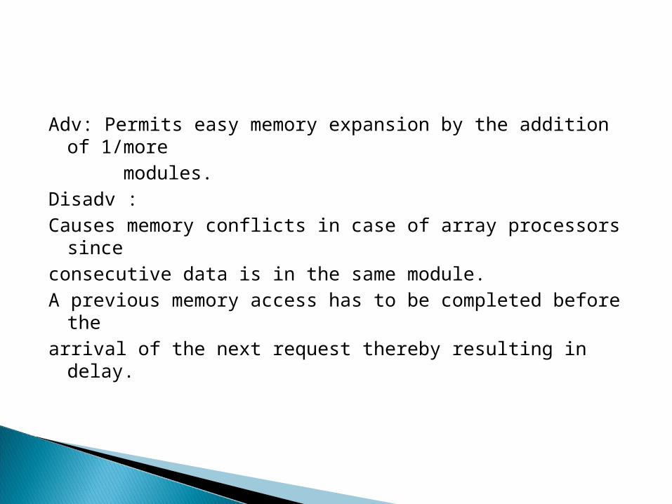
Adv: Permits easy memory expansion by the addition of 1/more modules.
Disadv : Causes memory conflicts in case of array processors since consecutive data is in the same module.A previous memory access has to be completed before the arrival of the next request thereby resulting in delay.
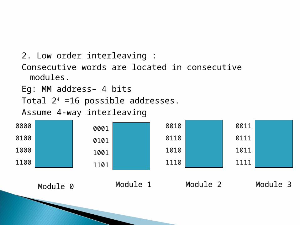
2. Low order interleaving :Consecutive words are located in consecutive modules.Eg: MM address– 4 bitsTotal 24 =16 possible addresses.Assume 4-way interleaving
0000
0100
1000
1100
0001
0101
1001
1101
0010
0110
1010
1110
0011
0111
1011
1111
Module 0 Module 1 Module 2 Module 3

The lower order k bits of an n-bit MM address select the module and higher order m-bits select address in module
Module Address in module
Module 0 Module 1 Module 2K-1
ABR ABR ABRDBR DBR DBR
m bits k bits
MM bits
Consecutive words in a module

AdvA request to access consecutive mem. Locations can keep
several modules busy at one time .Hence results in faster access to a block of data.

Paging is not (usually) visible to the programmer Segmentation is visible to the programmer. Segmentation is a memory management scheme that supports
user’s view of memory. Programmers never think of their programs as a linear array of
words. Rather, they think of their programs as a collection of logically related entities, such as subroutines or procedures, functions, global or local data areas, stack etc.
i.e they view programs as a collection of segments. A program consists of functions/subroutines , main program and data
which are required for the execution of the program. Each logical entity is a segment. Hence if we have a program consisting of 2 functions and an inbuilt
function sqrt. Then we have a segment for the main program, each of the
functions, data segment and a segment for sqrt.


1
4
2
3
user space physical memory space
1
3
2
4

Each segment has a name and a length. A logical address in segmentation is specified
1. A segment name (segment number)2. An offset within the segment
The user therefore specifies each address by 2 quantities : segment no. and the offset
When a user program is compiled, the compiler automatically constructs different segments reflecting the input program.

Conversion of logical address to physical address : This mapping is done with the help of a segment table. Every process has its own segment table. Each entry in the segment table has a segment base and a
segment limit. The segment base contains the starting physical address
where the segment resides in memory. Segment limit specifies the length of the segment.

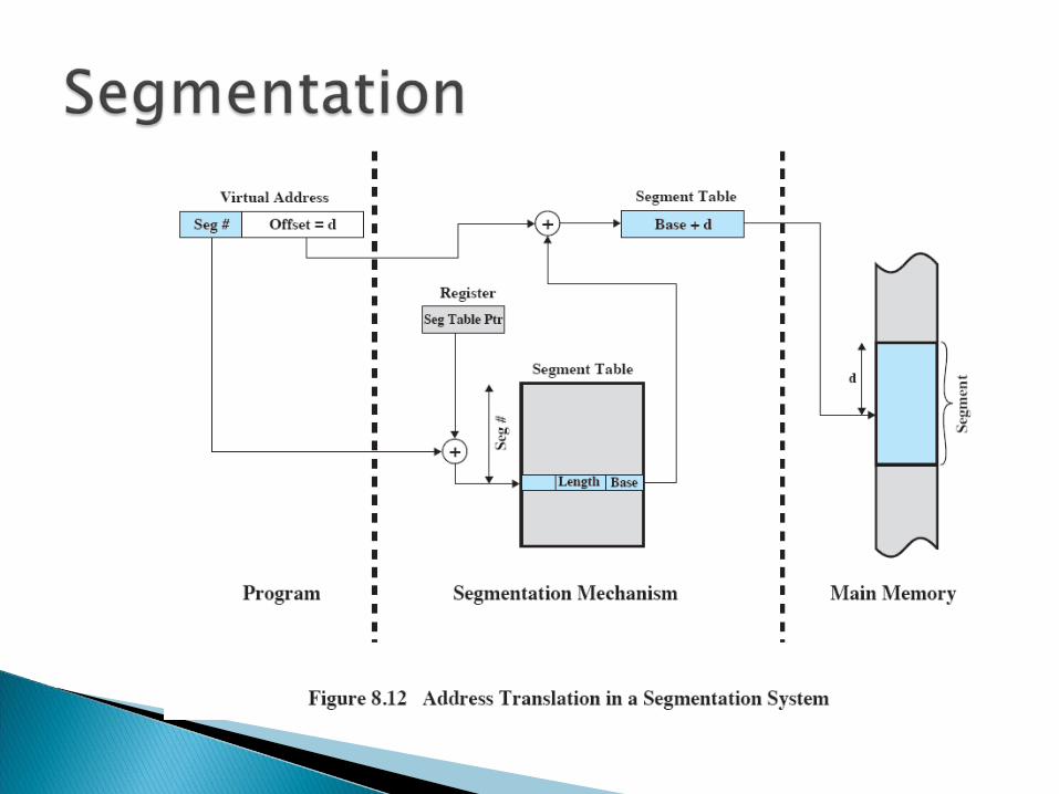

Eg: Segment 2 is 400 bytes long and begins at location(address) 4300.
A reference to byte no. 53 of segment 2 is mapped onto location 4300 + 53 =4353.
A reference to segment 3, byte 852, is mapped onto 3200 + 852=4052.
A reference to byte 1222 of segment 0 would result in a trap(interrupt) to the OS as this segment is only 1000 bytes.

External Fragmentation– total memory space exists to satisfy a request, but it is not contiguous.
Each segment is allocated a contiguous piece of physical memory. As segments are of different sizes swapping in/out of segments leads to holes in memory hence causes external fragmentation.
Memory allocation to a segment is done using first fit, worst fit and best fit strategy

The associative memory is also known as Content addressable memory.
It differs from other memories such as RAM, ROM, disk etc in the nature of accessing the memory and reading the content.
To any other memory, the address is given as input for reading the content of location. In the case of associative memory, usually a part of the content or the entire content is used for accessing the content.
The associative memory searches all the locations simultaneously in parallel
It is useful as a cache memory where in a search of the locations is needed to match with given TAG and TLB

- Accessed by the content of the data rather than by an address- Also called Content Addressable Memory (CAM)
Hardware Organization Argument register(A)
Key register (K)
Associative memoryarray and logic
m wordsn bits per word
Matchregister
Input
ReadWrite
- Compare each word in CAM in parallel with the content of A(Argument Register)
- If CAM Word[i] = A, M(i) = 1
- K(Key Register) provides a mask for choosing a particular field or key in the argument in A (only those bits in the argument that have 1’s in their corresponding position of K are compared)
Associative Memory

Fig shows the block diagram of associative memory of m locations of n bits each.
To perform a search operation, the argument is given to the argument register .
Two types of searches are possible◦ Searching on the entire argument◦ Searching on a part within the argument
The key register is supplied a mask pattern that indicates the bits of argument to be included for search pattern.
If any bit is 0 in the mask pattern, then the corresponding bits of the argument register should not be included in the search.

For an entire argument search, the key register is supplied all 1’s
While searching, the associative memory locates all the words which match the given argument and marks them by setting the corresponding bits in the match register
Example A = 10111100 K = 11100000 Word1 = 10011100 no match Word 2 = 101100001 match

Associative memory – parallel search
TLB
◦ If Page no is in associative register, get frame # out
◦ Otherwise get frame # from page table in memory
Page # Frame #

Example Associative memory(TLB)
PT of process id(0001)
Eg: if page 2 of pid 0001 is \\\\ searched for in the tlb to
find a matching frame no. Then input register will
have value 01000010000 Mask register -
11111110000
Page number
Frame number
000 1001
001
010 1000
011 0001
100
101 1101
110
111
Page number
PIDFrame number
000 0001 1001
010 0001 1000
011 0001 0001
101 0100 1101

Pipelining used in processors allow overlapping execution of multiple instructions.

Pipelined processor
IF ID OF EX

Space time diagram for non pipelined processor
I1
I1
I1
I1
I2
I2I2
I2
IF
ID
OF
EX
1
2
3 4
5
6
7
8 time

Space time diagram for pipelined processor
I1
I1
I1
I1
I2
I2
I2
I3IF
ID
OF
EX
I3
I4
time1
2
3 4
5
6
7
I2

Computers can be classified based on the instruction and data streams
This classification was first studied and proposed by Michael Flynn in 1972.
He introduced the concept of instruction and data streams for categorizing of computers.
Instruction Stream and Data Stream The term ‘stream’ refers to a sequence or flow of either
instructions or data operated on by the computer. In the complete cycle of instruction execution, a flow of
instructions from main memory to the CPU is established. This flow of instructions is called instruction stream.
Similarly, there is a flow of operands between processor and memory bi-directionally. This flow of operands is called data stream .

Thus, it can be said that the sequence of instructions executed by CPU forms the Instruction stream and the sequence of data (operands) required for execution of instructions form the Data streams.

Flynn’s Classification Flynn’s classification is based on multiplicity of instruction
streams and data streams observed by the CPU during program execution.
Let Is and Ds are streams flowing at any point in the execution, then the computer organization can be categorized as follows:
1. SISD- Single Instruction and Single Data stream2. SIMD- Single Instruction and Multiple Data stream3. MISD- Multiple Instruction and Single Data stream4. MIMD- Multiple Instruction and Multiple Data stream

SISD
Instructions are executed sequentially but may be overlapped in their execution stages.
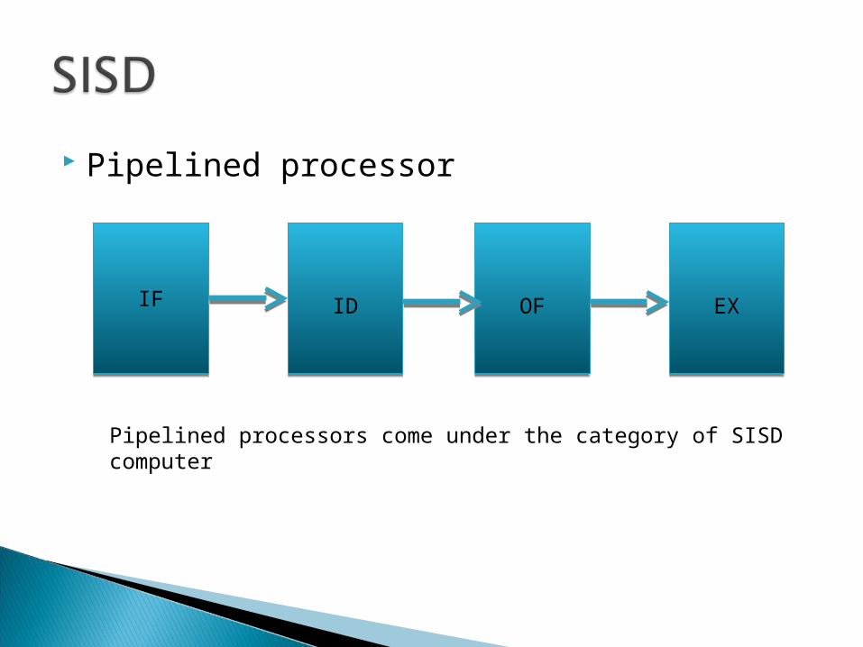
Pipelined processor
IF ID OF EX
Pipelined processors come under the category of SISD computer

SIMD•There are multiple processing elements supervised by the same control unit.•All PE’s receive the same instruction broadcast from the same control unit but operate on different data sets from distinct data streams.• The shared memory subsystem may contain multiple modules.

Eg:For (i=1; i<10; i++)c[i]= a[i]+b[i]In this example various iterations of the loop
are independent of each other. i.e c[1]=a[1] + b[1]c[2]=a[2]+b[2] and so on….In this case if there are 10 processing elements then the same instruction add could be executed on all on different data sets hence increasing the speed of execution

IS>1 Ds=1
There are n processors each receiving distinct instructions operating over the same data stream. The output of one processor become the input to the next and so on. No computers exists in this class

MIMD

Here each processing element is capable of executing a different program independent of the other processing element .
SIMD require less hardware and memory as compared to MIMD.
MIMD can be further classified as tightly coupled and loosely coupled
Tightly coupled- Processors share memory Loosely coupled- Each processor has it’s
own memory.